

Philips 74ahc ahct259 DATASHEETS

INTEGRATED CIRCUITS
DATA SH EET
74AHC259; 74AHCT259
8-bit addressable latch
Product specification
File under Integrated Circuits, IC06
2000 Mar 14

Philips Semiconductors Product specification
8-bit addressable latch
FEATURES
• ESD protection:
HBM EIA/JESD22-A114-A exceeds 2000 V
MM EIA/JESD22-A115-A exceeds 200 V
CDM EIA/JESD22-C101 exceeds 1000 V
• Balanced propagation delays
• All inputs have Schmitt-trigger actions
• Combines demultiplexer and 8-bit latch
• Serial-to-parallel capability
• Output from each storage bit available
• Random (addressable) data entry
• Easily expandable
• Common reset input
• Useful as a 3-to-8 active HIGH decoder
• Inputs accept voltages higher than V
• For AHC only: operates with CMOS input levels
• For AHCT only: operates with TTL input levels
• Specified from −40 to +85 °C and from −40 to +125 °C.
CC
74AHC259;
74AHCT259
DESCRIPTION
The 74AHC/AHCT259 are high-speed Si-gate CMOS
devices and are pin compatible with Low power Schottky
TTL (LSTTL). They are specified in compliance with
JEDEC standard No. 7A.
The 74AHC/AHCT259 are high-speed 8-bit addressable
latches designedfor general purpose storage applications
in digital systems. The ‘259’ are multifunctional devices
capable of storing single-line data in eight addressable
latches, and also 3-to-8 decoder and demultiplexer, with
active HIGH outputs (Q0 to Q7), functions are available.
The ‘259’ also incorporates an active LOW common reset
(MR) for resetting all latches as well as an active LOW
enable input (LE).
The ‘259’ has four modes of operation as shown in the
mode select table. Inthe addressable latchmode, data on
the data line (D) is written into the addressed latch. The
addressed latch will follow the data input with all nonaddressed latches remaining in their previous states.
In the memory mode, all latches remain in their previous
states and are unaffected by the data or address inputs.
In the 3-to-8 decoding or demultiplexing mode, the
addressed output follows the state of the (D) input with all
other outputs in the LOW state. In the reset mode all
outputs are LOW and unaffected by the address
(A0 to A2) and data (D) input. When operating the ‘259’ as
an address latch, changing more than one bit of the
address could impose a transient-wrong address.
Therefore, this should only be done while in the memory
mode.
The mode select table summarizes the operations of
the ‘259’.
2000 Mar 14 2
Philips Semiconductors Product specification
8-bit addressable latch
QUICK REFERENCE DATA
GND = 0 V; T
SYMBOL PARAMETER CONDITIONS
t
PHL/tPLH
C
I
C
O
C
PD
Notes
1. C
is used to determine the dynamic power dissipation (PDin µW).
PD
PD=CPD× V
fi= input frequency in MHz;
fo= output frequency in MHz;
∑ (CL× V
CL= output load capacitance in pF;
VCC= supply voltage in Volts.
2. The condition is VI= GND to VCC.
=25°C; tr=tf≤3.0 ns.
amb
propagation delay
DtoQn C
= 15 pF; VCC= 5 V 4.1 4.1 ns
L
An to Qn 5.3 5.5 ns
LE to Qn 4.3 4.3 ns
MR to Qn 3.9 3.9 ns
input capacitance VI=VCCor GND 3.0 3.0 pF
output capacitance 4.0 4.0 pF
power dissipation capacitance CL= 50 pF; f = 1 MHz; notes 1 and 2 13 17 pF
2
× fi+ ∑ (CL× V
CC
2
× fo) = sum of outputs;
CC
2
× fo) where:
CC
74AHC259;
74AHCT259
TYPICAL
UNIT
AHC AHCT
2000 Mar 14 3

Philips Semiconductors Product specification
8-bit addressable latch
74AHC259;
74AHCT259
FUNCTION TABLE
See note 1.
OPERATING MODE
MR LEDA0A1A2Q0Q1Q2Q3Q4Q5Q6Q7
reset L H XXXX LLLLLLLL
demultiplexer
(active HIGH
8-channel)
LL
decoder (when D = H)
memory (do nothing) H H XXXXq
addressable latch H L
INPUTS OUTPUTS
dLLLQ=dLLLLLLL
dHLLLQ=dLLLLLL
dLHLLLQ=dLLLLL
dHHLLLLQ=dLLLL
dLLHLLLLQ=dLLL
dHLHLLLLLQ=dLL
dLHHLLLLLLQ=dL
dHHHLLLLLLLQ=d
q1q2q3q4q5q6q
0
dLLLQ=dq
dHLLq0Q=d q
dLHLq0q1Q=d q
dHHLq0q1q2Q=d q
dLLHq0q1q2q3Q=d q
dHLHq0q1q2q3q4Q=d q
q2q3q4q5q6q
1
q
2
q
3
q
3
q
4
4
4
5
q
5
q
5
5
q
6
q
6
q
6
q
6
6
dLHHq0q1q2q3q4q5Q=d q
7
7
q
7
q
7
q
7
q
7
q
7
7
HHHHq0q1q2q3q4q5q6Q=d
Note
1. H = HIGH voltage level;
L = LOW voltage level;
X = don’t care;
d = HIGH or LOW data one set-up time prior to the LOW-to-HIGH LE transition;
q = lower case letters indicate the state of the referenced output established during the last cycle in which it was
addressed or cleared.
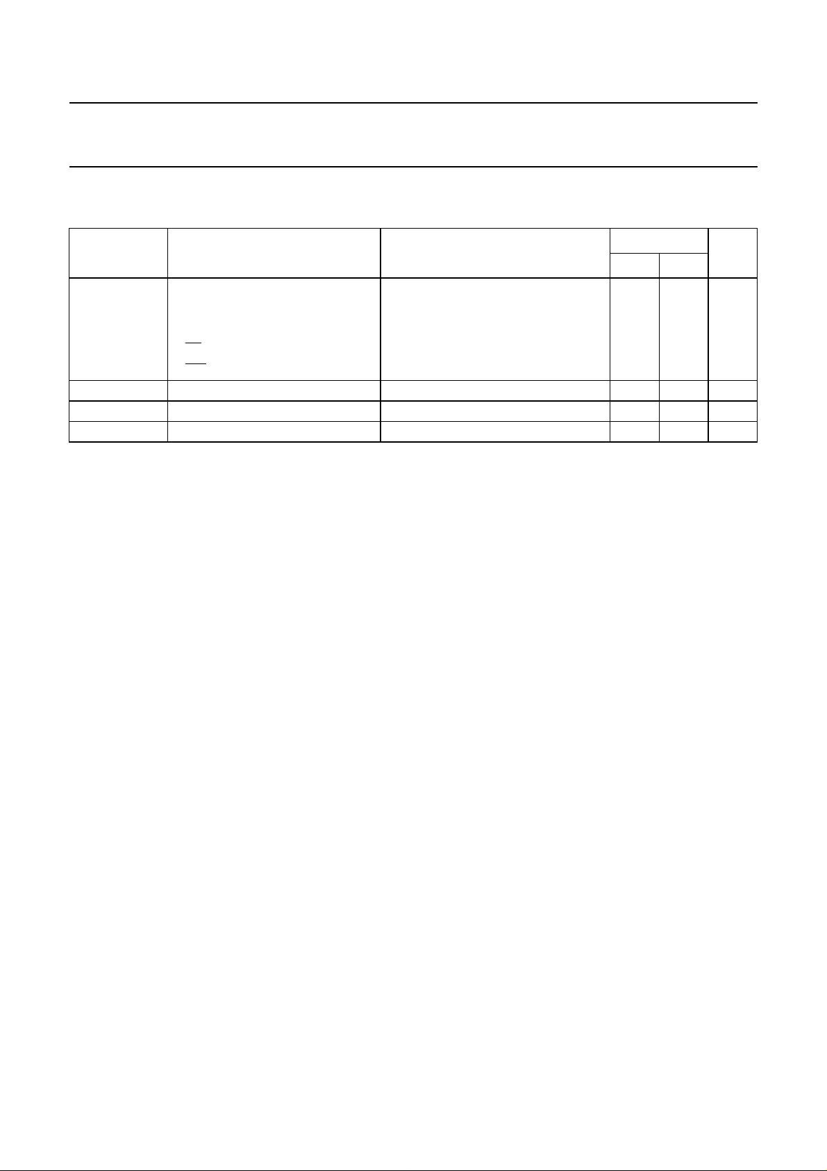
ORDERING INFORMATION
PACKAGES
TYPE NUMBER
TEMPERATURE
RANGE
PINS PACKAGE MATERIAL CODE
74AHC259D −40 to +125 °C 16 SO plastic SOT109-1
74AHC259PW 16 TSSOP plastic SOT403-1
74AHCT259D 16 SO plastic SOT109-1
74AHCT259PW 16 TSSOP plastic SOT403-1
2000 Mar 14 4
Philips Semiconductors Product specification
8-bit addressable latch
PINNING
PIN SYMBOL DESCRIPTION
1, 2 and 3 A0, A1 and A2 address input
4, 5, 6, 7, 9, 10, 11 and 12 Q0 to Q7 latch outputs
8 GND ground (0 V)
13 D data input
14
15
16 V
handbook, halfpage
A0
A1
A2
Q0
Q1
Q2
Q3
GND
1
2
3
4
259
5
6
7
8
MNA574
LE latch enable input (active LOW)
MR conditional reset input (active LOW)
CC
V
16
CC
15
MR
14
LE
D
13
12
Q7
11
Q6
Q5
10
Q4
9
handbook, halfpage
DC supply voltage
LE
13
D
1
A0
2
A1
3
A2
MR
74AHC259;
74AHCT259
14
4
Q0
5
Q1
6
Q2
7
Q3
9
Q4
10
Q5
11
Q6
12
Q7
15
MNA573
Fig.1 Pin configuration.
2000 Mar 14 5
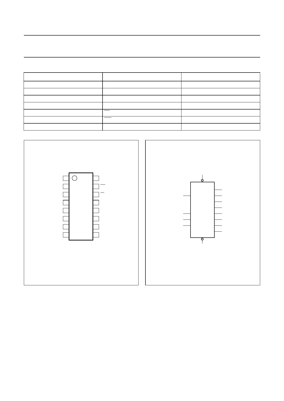
Fig.2 Logic symbol.

Philips Semiconductors Product specification
8-bit addressable latch
handbook, halfpage
1
2
3
13
Z9
15
G8
14
G10
DX
0
0
G
7
2
9,10D
0
1
2
3
4
5
6
7
74AHC259;
74AHCT259
handbook, halfpage
A0
C10
1
8R
MNA572
4
5
6
7
9
10
11
12
1
A1
2
3
14
15
13
A2
LE
MR
D
1-of-8
DECODER
8 LATCHES
Q0
Q1
Q2
Q3
Q4
Q5
Q6
Q7
MNA571
4
5
6
7
9
10
11
12
Fig.3 IEC logic symbol.
OPERATING MODE SELECT TABLE
LE MR MODE
L H addressable latch
H H memory
L L active HIGH 8-channel demultiplexer
H L reset
Note
1. H = HIGH voltage level;
L = LOW voltage level.
Fig.4 Functional diagram.
2000 Mar 14 6
 Loading...