

Philips 74ahc ahct1g06 DATASHEETS

INTEGRATED CIRCUITS
DATA SH EET
74AHC1G06; 74AHCT1G06
Inverter with open-drain output
Product specification
File under Integrated Circuits, IC06
2000 May 01

Philips Semiconductors Product specification
Inverter with open-drain output
FEATURES
• High noise immunity
• ESD protection:
HBM EIA/JESD22-A114-A exceeds 2000 V
MM EIA/JESD22-A115-A exceeds 200 V
• Low power dissipation
• SOT353 package
• Output capability standard (open drain).
QUICK REFERENCE DATA
GND = 0 V; T
=25°C; tr=tf≤3.0 ns.
amb
SYMBOL PARAMETER CONDITIONS
t
t
C
C
PZL
PLZ
I
PD
propagation delay inA to outY CL= 15 pF; VCC= 5 V 2.7 3.0 ns
propagation delay inA to outY CL= 15 pF; VCC= 5 V 3.0 3.2 ns
input capacitance 1.5 1.5 pF
power dissipation capacitance CL= 50 pF; f = 1 MHz;
notes 1 and 2
DESCRIPTION
The74AHC1G/AHCT1G06isahigh-speedSi-gateCMOS
device.
The 74AHC1G/AHCT1G06 provides the inverting buffer.
The output of the 74AHC1G/AHCT1G06 devices is an
open drain and can be connected to other open-drain
outputs to implement active-LOW, wired-OR or
active-HIGH wired-AND functions. For digital operation
this device must have a pull-up resistor to establish a logic
HIGH-level.
74AHC1G06;
74AHCT1G06
TYPICAL
UNIT
AHC1G AHCT1G
3 4.5 pF
Notes
1. C
is used to determine the dynamic power dissipation (PDin µW).
PD
PD=CPD× V
= input frequency in MHz;
f
i
2
× fi+(CL×V
CC
CC
fo= output frequency in MHz;
CL= output load capacitance in pF;
VCC= supply voltage in Volts.
2. The condition is VI= GND to VCC.
FUNCTION TABLE
See note 1.
INPUT OUTPUT
inA outY
LZ
HL
Note
1. H = HIGH voltage level;
L = LOW voltage level;
Z = high impedance OFF-state.
2
× fo) where:
2000 May 01 2
Philips Semiconductors Product specification
Inverter with open-drain output
74AHC1G06;
74AHCT1G06
ORDERING AND PACKAGE INFORMATION
PACKAGES
TYPE NUMBER
74AHC1G06GW −40 to +125 °C 5 SC-88A plastic SOT353 AR
74AHCT1G06GW 5 SC-88A plastic SOT353 CR
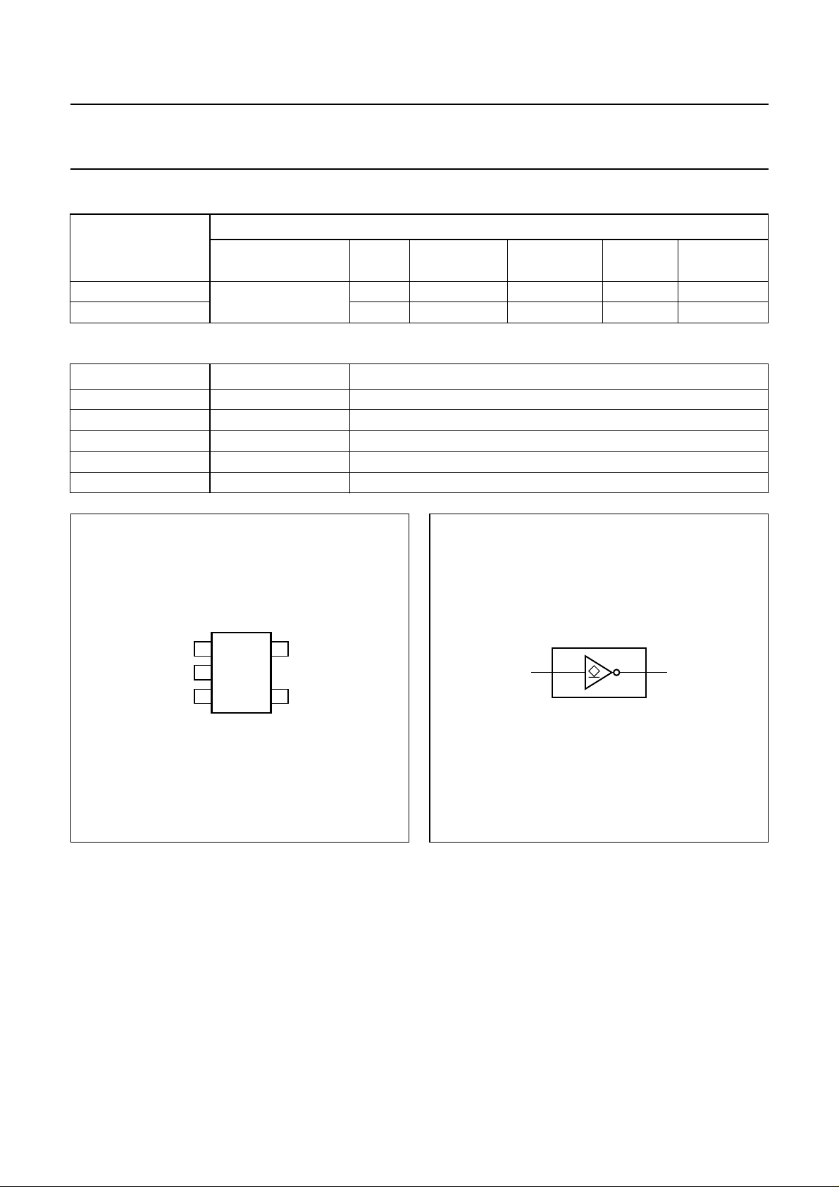
PINNING
PIN SYMBOL DESCRIPTION
1 n.c. not connected
2 inA data input
3 GND ground (0 V)
4 outY data output
5V
TEMPERATURE
RANGE
CC
PINS PACKAGE MATERIAL CODE MARKING
DC supply voltage
handbook, halfpage
n.c.
inA
GND
1
2
06
3
MNA583
V
5
outY
4
Fig.1 Pin configuration.
CC
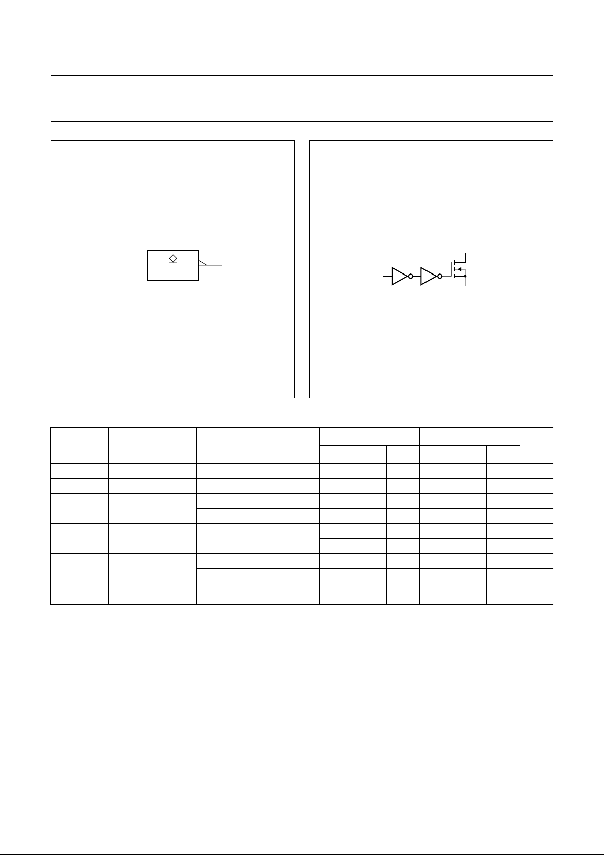
handbook, halfpage
inA outY
2
MNA584
Fig.2 Logic symbol.
4
2000 May 01 3
Philips Semiconductors Product specification
Inverter with open-drain output
handbook, halfpage
2
inA
MNA585
Fig.3 IEC logic symbol.
4
outY
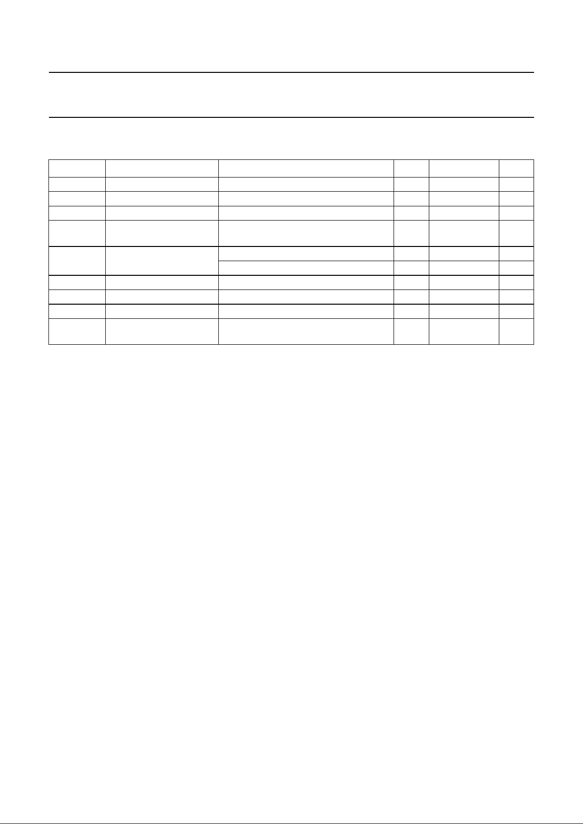
handbook, halfpage
inA
Fig.4 Logic diagram.
74AHC1G06;
74AHCT1G06
outY
MNA586
GND
RECOMMENDED OPERATING CONDITIONS
SYMBOL PARAMETER CONDITIONS
V
CC
V
I
V
O
DC supply voltage 2.0 5.0 5.5 4.5 5.0 5.5 V
input voltage 0 − 5.5 0 − 5.5 V
output voltage active mode 0 − V
high-impedance mode 0 − 6.0 0 − 6.0 V
T
amb
tr, tf (∆t/∆f) input rise and fall
operating ambient
temperature
time ratios (except
for Schmitt-trigger
see DC and AC
characteristics per device
VCC= 3.3 ±0.3 V −−100 −−−ns/V
=5±0.5 V −−20 −−20 ns/V
V
CC
inputs)
74AHC 74AHCT
UNIT
MIN. TYP. MAX. MIN. TYP. MAX.
0 − V
CC
CC
V
−40 +25 +85 −40 +25 +85 °C
−40 +25 +125 −40 +25 +125 °C
2000 May 01 4
Philips Semiconductors Product specification
Inverter with open-drain output
74AHC1G06;
74AHCT1G06
LIMITING VALUES
In accordance with the Absolute Maximum Rating System (IEC 60134); voltages are referenced to GND (ground = 0 V).
SYMBOL PARAMETER CONDITIONS MIN. MAX. UNIT
V
CC
V
I
I
IK
I
OK
V
O
I
O
I
CC
T
stg
P
D
Notes
1. The input and output voltage ratings may be exceeded if the input and output current ratings are observed.
2. Above 55 °C the value of P
DC supply voltage −0.5 +7.0 V
input voltage −0.5 +7.0 V
DC input diode current VI< −0.5 V; note 1 −−20 mA
DC outputclampingdiode
VO< −0.5 V; note 1 −±20 mA
current
output voltage active mode; note 1 −0.5 VCC+ 0.5 V
high-impedance mode; note 1 −0.5 7.0 V
DC output sink current VO> −0.5 V −±25 mA
DC VCC or GND current −±75 mA
storage temperature −65 +150 °C
power dissipation per
package
derates linearly with 2.5 mW/K.
D
for temperature range: −40 to +125 °C;
note 2
− 200 mW
2000 May 01 5
 Loading...