

Philips 74ahc ahct139 DATASHEETS

INTEGRATED CIRCUITS
DATA SH EET
74AHC139; 74AHCT139
Dual 2-to-4 line
decoder/demultiplexer
Product specification
File under Integrated Circuits, IC06
1999 Sep 01

Philips Semiconductors Product specification
Dual 2-to-4 line decoder/demultiplexer
FEATURES
• ESD protection:
HBM EIA/JESD22-A114-A exceeds 2000 V
MM EIA/JESD22-A115-A exceeds 200 V
CDM EIA/JESD22-C101 exceeds 1000 V
• Balanced propagation delays
• All inputs have Schmitt trigger actions
• Inputs accept voltages higher than V
• For AHC only: operates with CMOS input levels
• For AHCT only: operates with TTL input levels
• Specified from −40 to +85 °C and −40 to +125 °C.
QUICK REFERENCE DATA
Ground = 0 V; T
=25°C; tr=tf≤ 3.0 ns.
amb
CC
74AHC139;
74AHCT139
DESCRIPTION
The 74AHC/AHCT139 are high-speed Si-gate CMOS
devices and are pin compatible with low power Schottky
TTL (LSTTL). They are specified in compliance with
JEDEC standard no. 7A.
The 74AHC/AHCT139 are high-speed, dual 2-to-4 line
decoder/demultiplexers.
This device has two independent decoders, each
accepting two binary weighted inputs (nA0 and nA1) and
providing four mutually exclusive active LOW outputs
(nY0to nY3). Each decoder has an active LOW enable
input(nE).When nEis HIGH, every output is forced HIGH.
The enable input can be used as the data input for a 1-to-4
demultiplexer application.
The ‘139’ is identical to the HEF4556 of the HE4000B
family.
SYMBOL PARAMETER CONDITIONS
t
PHL/tPLH
C
I
C
O
C
PD
propagation delay CL= 15 pF; VCC=5V
nAnto nY
n
EtonY
n
n
input capacitance VI=VCCor GND 3.0 3.0 pF
output capacitance 4.0 4.0 pF
power dissipation capacitance CL= 50 pF; f = 1 MHz;
notes 1 and 2
Notes
1. C
is used to determine the dynamic power dissipation (PDin µW).
PD
PD=CPD× V
2
× fi+ ∑ (CL× V
CC
2
× fo) where:
CC
fi= input frequency in MHz;
fo= output frequency in MHz;
∑ (CL× V
2
× fo) = sum of outputs;
CC
CL= output load capacitance in pF;
VCC= supply voltage in Volts.
2. The condition is VI= GND to VCC.
TYPICAL
UNIT
AHC AHCT
3.9 4.7 ns
3.4 3.6 ns
25.76 22.36 pF
1999 Sep 01 2
Philips Semiconductors Product specification
Dual 2-to-4 line decoder/demultiplexer
74AHC139;
74AHCT139
FUNCTION TABLE
See note 1.
INPUTS OUTPUTS
nEnA0nA
1
HXXHHHH
LLLLHHH
LHLHLHH
LLHHHLH
LHHHHHL
Note
1. H = HIGH voltage level;
L = LOW voltage level;
X = don’t care.
ORDERING INFORMATION
OUTSIDE NORTH
AMERICA
NORTH AMERICA
74AHC139D 74AHC139D 16 SO plastic SOT109-1
74AHC139PW 74AHC139PW DH 16 TSSOP plastic SOT403-1
74AHCT139D 74AHCT139D 16 SO plastic SOT109-1
74AHCT139PW 74AHCT139PW DH 16 TSSOP plastic SOT403-1
nY
0
nY
1
nY
2
nY
3
PACKAGES
PINS PACKAGE MATERIAL CODE
PINNING
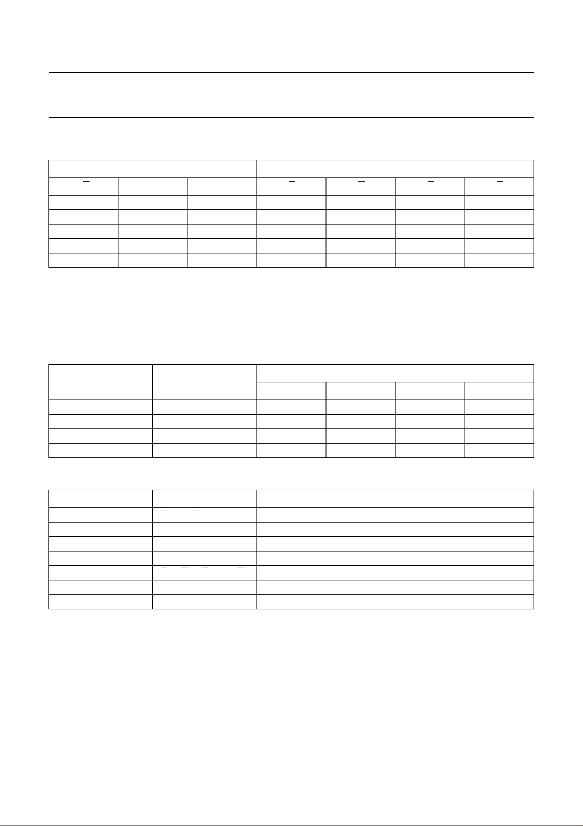
PIN SYMBOL DESCRIPTION
1 and 15 1E and 2E enable inputs (active LOW)
2 and 3 1A0and 1A
1
4, 5, 6 and 7 1Y0, 1Y1, Y2and 1Y
address inputs
outputs (active LOW)
3
8 GND ground (0 V)
9, 10, 11 and 12 2Y3, 2Y2, 2Y1and 2Y0outputs (active LOW)
13 and 14 2A1and 2A
16 V
CC
0
address inputs
DC supply voltage
1999 Sep 01 3
Philips Semiconductors Product specification
Dual 2-to-4 line decoder/demultiplexer
handbook, halfpage
1E
1A
1A
1Y
1Y
1Y
1Y
GND
1
2
0
3
1
4
0
1
2
3
139
5
6
7
8
MNA465
V
16
CC
15
2E
2A
14
0
2A
13
1
12
2Y
0
11
2Y
1
2Y
10
2
2Y
9
3
handbook, halfpage
74AHC139;
74AHCT139
1
1E
2
1A
3
1A
14
2A
13
2A
1Y
1Y
0
1Y
1
1Y
2Y
2Y
0
2Y
1
2Y
2E
15
0
1
2
3
0
1
2
3
MNA466
4
5
6
7
12
11
10
9
handbook, halfpage
2
3
1
14
13
15
Fig.1 Pin configuration.
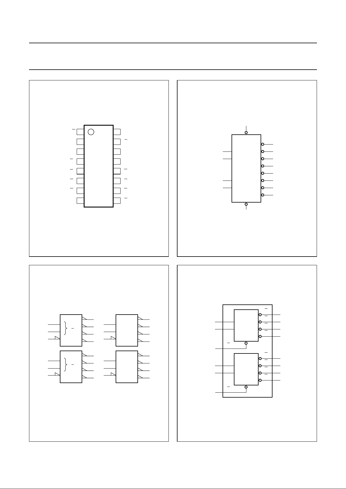
DX
0
0
G
3
1
DX
0
0
G
3
1
(a) (b)
4
0
1
2
3
12
0
11
1
10
2
3
2
5
3
6
1
7
14
13
15
9
1
2
EN
1
2
EN
X/Y
X/Y
0
1
2
3
0
1
2
3
12
11
10
MNA467
Fig.2 Logic symbol.
handbook, halfpage
4
5
6
7
9
1A
0
2
1A
3
1
1E
1
2A
0
14
2A
13
1
2E
15
1Y
1Y
1Y
1Y
2Y
2Y
2Y
2Y
MNA468
4
0
5
1
6
2
7
3
12
0
11
1
10
2
9
3
Fig.3 IEC logic symbol.
1999 Sep 01 4
Fig.4 Functional diagram.

Philips Semiconductors Product specification
Dual 2-to-4 line decoder/demultiplexer
74AHC139;
74AHCT139
RECOMMENDED OPERATING CONDITIONS
SYMBOL PARAMETER CONDITIONS
V
CC
V
I
V
O
T
amb
DC supply voltage 2.0 5.0 5.5 4.5 5.0 5.5 V
input voltage 0 − 5.5 0 − 5.5 V
output voltage 0 − V
operating ambient
temperature
see DC and AC
characteristics per device
tr,tf (∆t/∆f) input rise and fall ratio VCC= 3.3 ±0.3 V −−100 −−−ns/V
VCC=5±0.5 V −−20 −−20
LIMITING VALUES
In accordance with the Absolute Maximum Rating System (IEC 134); voltages are referenced to GND (ground = 0 V).
SYMBOL PARAMETER CONDITIONS MIN. MAX. UNIT
V
CC
V
I
I
IK
I
OK
I
O
I
CC
T
stg
P
D
DC supply voltage −0.5 +7.0 V
input voltage −0.5 +7.0 V
DC input diode current VI< −0.5 V; note 1 −−20 mA
DC output diode current VO< −0.5 Vor VO>VCC+ 0.5 V; note 1 −±20 mA
DC output source or sink current −0.5V<VO<VCC+ 0.5 V −±25 mA
DC VCC or GND current −±75 mA
storage temperature −65 +150 °C
power dissipation per package for temperature range: −40 to +125 °C;
note 2
74AHC 74AHCT
UNIT
MIN. TYP. MAX. MIN. TYP. MAX.
0 − V
CC
CC
V
−40 +25 +85 −40 +25 +85 °C
−40 +25 +125 −40 +25 +125 °C
− 500 mW
Notes
1. The input and output voltage ratings may be exceeded if the input and output current ratings are observed.
2. For SO package: above 70 °C the value of PD derates linearly with 8 mW/K.
For TSSOP package: above 60 °C the value of PD derates linearly with 5.5 mW/K.
1999 Sep 01 5
 Loading...