

Philips 74AHCT74, 74AHC74 Datasheet

INTEGRATED CIRCUITS
DATA SH EET
74AHC74; 74AHCT74
Dual D-type flip-flop with set and
reset; positive-edge trigger
Product specification
Supersedes data of 1999 Aug 05
File under Integrated Circuits, IC06
1999 Sep 23
Philips Semiconductors Product specification
Dual D-type flip-flop with set and reset;
positive-edge trigger
FEATURES
• ESD protection:
HBM EIA/JESD22-A114-A
exceeds 2000 V
MM EIA/JESD22-A115-A
exceeds 200 V
• Balanced propagation delays
• Inputsacceptsvoltageshigherthan
V
CC
• For AHC only:
operates with CMOS input levels
• For AHCT only:
operates with TTL input levels
• Output capability: standard
• ICC category: flip-flops
• Specified from
−40 to +85 and +125 °C.
DESCRIPTION
The 74AHC/AHCT74 are high-speed
Si-gate CMOS devices and are pin
compatible with low power Schottky
TTL (LSTTL). They are specified in
compliance with JEDEC standard
No. 7A.
The 74AHC/AHCT74 dual
positive-edge triggered, D-type
flip-flops with individual data (D)
inputs,clock (CP)inputs,set (SD)and
reset (RD) inputs; also
complementary Q and Q outputs.
The set and reset are asynchronous
active LOW inputs and operate
independently of the clock input.
Information on the data input is
transferred to the Q output on the
LOW-to-HIGH transition of the clock
pulse. The D inputs must be stable
one set-up time prior to the
LOW-to-HIGH clock transition for
predictable operation.
Schmitt-trigger action in the clock
input makes the circuit highly tolerant
to slower clock rise and fall times.
QUICK REFERENCE DATA
GND = 0 V; T
=25°C; tr=tf≤3.0 ns.
amb
SYMBOL PARAMETER CONDITIONS
t
PHL/tPLH
propagation delay CL= 15 pF;
nCP to nQ, n
n
SD,nRDto nQ, nQ 3.7 3.7 ns
f
max
C
C
I
PD
max. clock frequency 130 100 MHz
input capacitance VI=VCCor GND 4.0 4.0 pF
power dissipation
capacitance
Notes
1. C
is used to determine the dynamic power dissipation (PDin µW).
PD
PD=CPD× V
CC
fi= input frequency in MHz; fo= output frequency in MHz;
∑ (CL× V
2
× fo) = sum of outputs;
CC
CL= output load capacitance in pF;
VCC= supply voltage in Volts.
2. The condition is VI= GND to VCC.
FUNCTION TABLES
Table 1 See note 1
S
n
D
nR
LHXXHL
HLXXLH
LLXXHH
Table 2 See note 1
S
n
D
nR
HH↑LLH
HH↑HHL
Note to Tables 1 and 2
1. H = HIGH voltage level;
L = LOW voltage level;
X = don’t care;
↑ = LOW-to-HIGH CP transition;
= state after the next LOW-to-HIGH CP transition.
Q
n+1
74AHC74; 74AHCT74
TYPICAL
AHC AHCT
Q 3.7 3.3 ns
2
× fi+ ∑ (CL× V
INPUT OUTPUT
D
INPUT OUTPUT
D
VCC=5V
CL= 50 pF;
12 16 pF
f = 1 MHz;
notes 1 and 2
2
× fo) where:
CC
nCP nD nQ nQ
nCP nD nQ
n+1
nQ
UNIT
n+1
1999 Sep 23 2
Philips Semiconductors Product specification
Dual D-type flip-flop with set and reset;
74AHC74; 74AHCT74
positive-edge trigger
ORDERING INFORMATION
OUTSIDE
NORTH
AMERICA
NORTH AMERICA
TEMPERATURE
RANGE
PINS PACKAGE MATERIAL CODE
74AHC74D 74AHC74D −40 to +85 °C 14 SO plastic SOT108-1
74AHC74PW 74AHC74PW DH 14 TSSOP plastic SOT402-1
74AHCT74D 74AHCT74D 14 SO plastic SOT108-1
74AHCT74PW 74AHCT74PW DH 14 TSSOP plastic SOT402-1
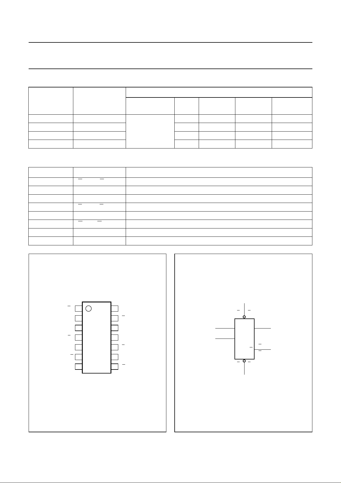
PINNING
PIN SYMBOL DESCRIPTION
1 and 13 1
RDand 2R
D
asynchronous reset-direct input (active LOW)
2 and 12 1D and 2D data inputs
3 and 11 1CPand 2CP clock input (LOW-to-HIGH, edge-triggered)
4 and 10 1
SDand 2S
D
asynchronous set-direct input (active LOW)
5 and 9 1Q and 2Q true flip-flop outputs
6 and 8 1
Q and 2Q complement flip-flop outputs
7 GND ground (0 V)
14 V
CC
DC supply voltage
PACKAGE
handbook, halfpage
1R
1D
1CP
1S
1Q
1Q
GND
1
D
2
3
4
D
74
5
6
7
MNA417
14
V
CC
13
2R
D
12
2D
11
2CP
2S
10
D
9
2Q
8
2Q
Fig.1 Pin configuration.
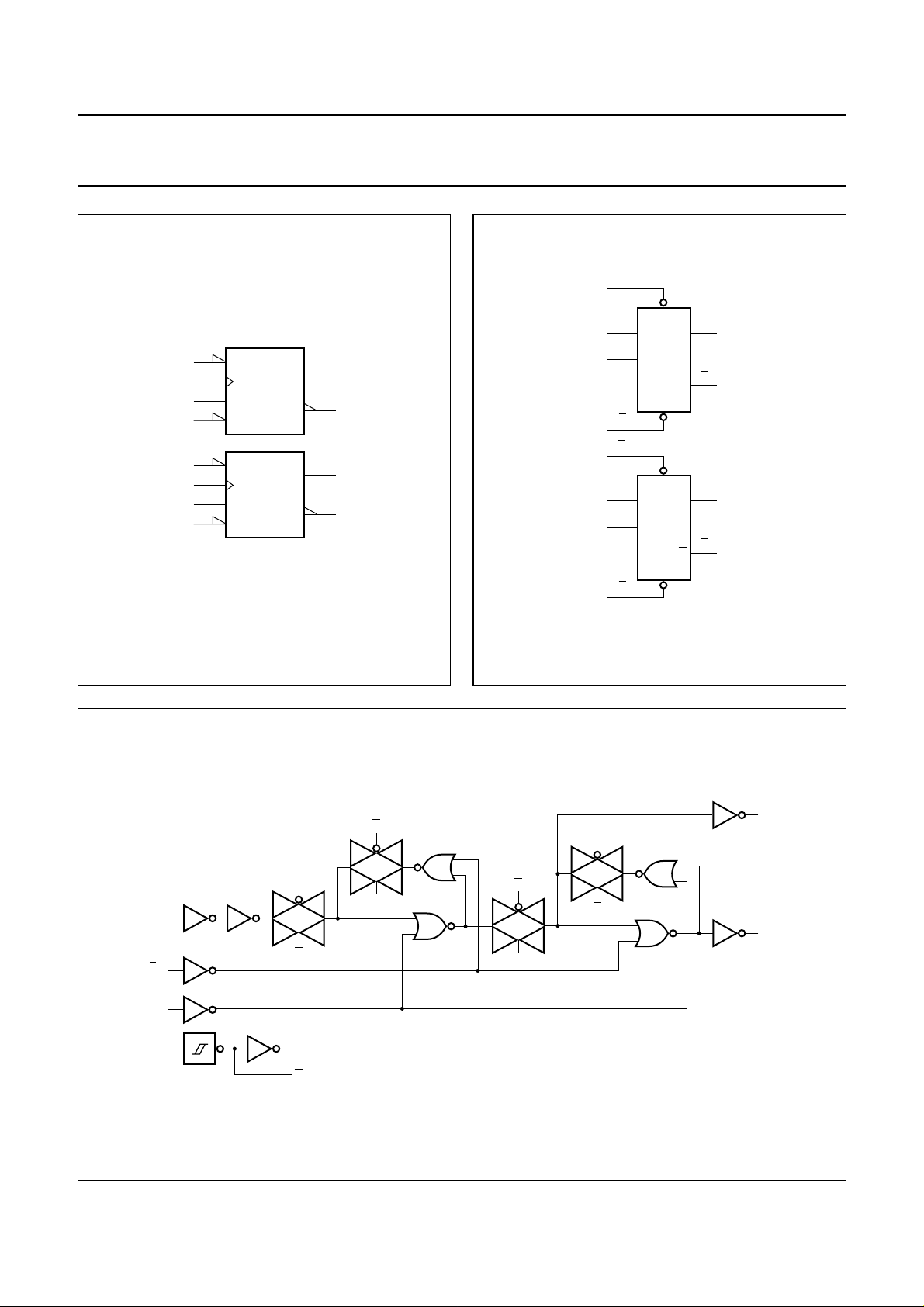
1999 Sep 23 3
handbook, halfpage
410
2S
1S
D
D
S
D
FF
R
D
2R
D
113
Q
Q
D
1Q
2Q
1Q
2Q
MNA418
2
1D
2D
1CP
2CP
D
CP
1R
12
3
11
Fig.2 Logic diagram.
5
9
6
8
Philips Semiconductors Product specification
Dual D-type flip-flop with set and reset;
positive-edge trigger
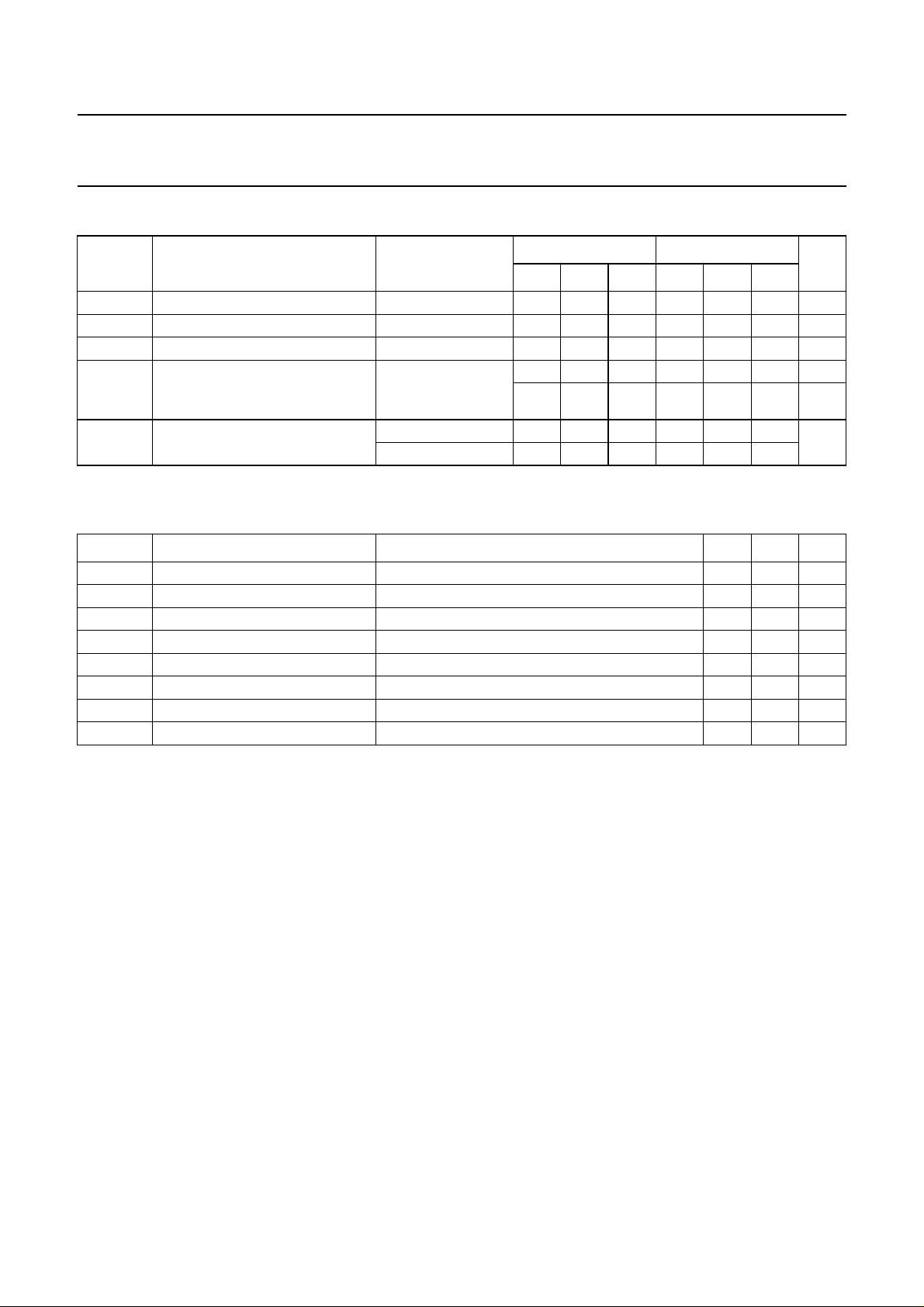
handbook, halfpage
4
S
3
C1
2
1D
1
R
10
S
11
C1
12
1D
13
R
MNA419
5
6
9
8
handbook, halfpage
74AHC74; 74AHCT74
1S
D
4
S
D
1D
2
D
1CP
CP
3
1R
D
1
2S
D
10
2D
12
11
13
2CP
2R
D
CP
D
1Q
Q
5
FF
1Q
6
Q
R
D
S
D
2Q
9
Q
FF
2Q
8
Q
R
D
MNA420
handbook, full pagewidth
D
R
D
S
D
CP
Fig.3 IEC logic symbol.
C
C
C
C
Fig.4 Functional diagram.
C
C
C
C
C
C
MNA421
Q
Q
Fig.5 Logic diagram (one flip-flop).
1999 Sep 23 4
Philips Semiconductors Product specification
Dual D-type flip-flop with set and reset;
74AHC74; 74AHCT74
positive-edge trigger
RECOMMENDED OPERATING CONDITIONS
SYMBOL PARAMETER CONDITIONS
V
CC
V
I
V
O
T
amb
DC supply voltage 2.0 5.0 5.5 4.5 5.0 5.5 V
input voltage 0 − 5.5 0 − 5.5 V
output voltage 0 − V
operating ambient temperature see DC and AC
characteristics per
device
t
(∆t/∆f) input rise and fall rates VCC= 3.3 V ±0.3 V −−100 −−−ns/V
r,tf
=5V±0.5 V −−20 −−20
V
CC
LIMITING VALUES
In accordance with the Absolute Maximum Rating System (IEC 134); voltages are referenced to GND (ground= 0 V).
SYMBOL PARAMETER CONDITIONS MIN. MAX. UNIT
V
CC
V
I
I
IK
I
OK
I
O
I
CC
T
stg
P
D
DC supply voltage −0.5 +7.0 V
input voltage −0.5 +7.0 V
DC input diode current VI< −0.5 V; note 1 −−20 mA
DC output diode current VO< −0.5 Vor VO>VCC+ 0.5 V; note 1 −±20 mA
DC output source or sink current −0.5V<VO<VCC+ 0.5 V −±25 mA
DC VCC or GND current −±75 mA
storage temperature −65 +150 °C
power dissipation per package for temperature range: −40 to +85 °C; note 2 − 500 mW
74AHC 74AHCT
UNIT
MIN. TYP. MAX. MIN. TYP. MAX.
0 − V
CC
CC
V
−40 +25 +85 −40 +25 +85 °C
−40 +25 +125 −40 +25 +125 °C
Notes
1. The input and output voltage ratings may be exceeded if the input and output current ratings are observed.
2. For SO packages: above 70 °C the value of P
derates linearly with 8 mW/K.
D
For TSSOP packages: above 60 °C the value of PDderates linearly with 5.5 mW/K.
1999 Sep 23 5
Philips Semiconductors Product specification
Dual D-type flip-flop with set and reset;
74AHC74; 74AHCT74
positive-edge trigger
DC CHARACTERISTICS
74AHC family
Over recommended operating conditions; voltage are referenced to GND (ground = 0 V).
SYMBOL PARAMETER
V
IH
HIGH-level input
voltage
V
IL
LOW-level input
voltage
V
OH
HIGH-level output
voltage; all
outputs
HIGH-level output
voltage
V
OL
LOW-level output
voltage; all
outputs
LOW-level output
voltage
I
I
input leakage
current
I
OZ
3-state output
OFF current
I
CC
quiescent supply
current
C
I
input capacitance −−310−10 − 10 pF
TEST CONDITIONS T
25 −40 to +85 −40 to +125
OTHER VCC(V)
MIN. TYP. MAX. MIN. MAX. MIN. MAX.
2.0 1.5 −−1.5 − 1.5 − V
3.0 2.1 −−2.1 − 2.1 −
5.5 3.85 −−3.85 − 3.85 −
2.0 −− 0.5 − 0.5 − 0.5 V
3.0 −− 0.9 − 0.9 − 0.9
5.5 −− 1.65 − 1.65 − 1.65
VI=VIHor VIL;
IO= −50 µA
2.0 1.9 2.0 − 1.9 − 1.9 − V
3.0 2.9 3.0 − 2.9 − 2.9 −
4.5 4.4 4.5 − 4.4 − 4.4 −
V
I=VIH
or VIL;
3.0 2.58 −−2.48 − 2.40 − V
IO= −4.0 mA
V
I=VIH
or VIL;
4.5 3.94 −−3.8 − 3.70 −
IO= −8.0 mA
VI=VIHor VIL;
IO=50µA
2.0 − 0 0.1 − 0.1 − 0.1 V
3.0 − 0 0.1 − 0.1 − 0.1
4.5 − 0 0.1 − 0.1 − 0.1
V
I=VIH
or VIL;
3.0 −− 0.36 − 0.44 − 0.55 V
IO=4mA
V
I=VIH
or VIL;
4.5 −− 0.36 − 0.44 − 0.55
IO=8mA
VI=VCCor GND 5.5 −− 0.1 − 1.0 − 2.0 µA
VI=VIHor VIL;
5.5 −− ±0.25 −±2.5 −±10.0 µA
VO=VCCor GND
VI=VCCor GND;
5.5 −− 2.0 − 20 − 40 µA
IO=0
amb
(°C)
UNIT
1999 Sep 23 6
 Loading...