

Philips 74AHCT373PW, 74AHCT373D, 74AHC373PW, 74AHC373D Datasheet

INTEGRATED CIRCUITS
DATA SH EET
74AHC373; 74AHCT373
Octal D-type transparent latch;
3-state
Product specification
Supersedes data of 1998 Dec 11
File under Integrated Circuits, IC06
1999 Nov 23
Philips Semiconductors Product specification
Octal D-type transparent latch; 3-state 74AHC373; 74AHCT373
FEATURES
• ESD protection:
HBM EIA/JESD22-A114-A exceeds 2000 V
MM EIA/JESD22-A115-A exceeds 200 V
CDM EIA/JESD22-C101 exceeds 1000 V
• Balanced propagation delays
• All inputs have Schmitt-trigger actions
• Inputs accepts voltages higher than V
CC
• Common 3-state output enable input
• Functionally identical to the ‘533’, ‘563’ and ‘573’
• For AHC only: operates with CMOS input levels
• For AHCT only: operates with TTL input levels
• Specified from −40 to +85 °C and −40 to +125 °C.
DESCRIPTION
The 74AHC/AHCT373 are high-speed Si-gate CMOS
devices and are pin compatible with Low power Schottky
TTL (LSTTL). They are specified in compliance with
JEDEC standard no. 7A.
QUICK REFERENCE DATA
Ground = 0 V; T
=25°C; tr=tf≤3.0 ns.
amb
The 74AHC/AHCT373 are octal D-type transparent
latchesfeaturingseparateD-typeinputsforeachlatchand
3-state outputs for bus oriented applications. A Latch
Enable (LE) input and an Output Enable (OE) input are
common to all latches.
The ‘373’ consists of eight D-type transparent latches with
3-state true outputs. When LE is HIGH, data at the
Dninputs enters the latches. In this condition the latches
are transparent, i.e. a latch output will change state each
time its corresponding D-input changes.
When LE is LOW the latches store the information that
was present at the D-inputs a set-up time preceding the
HIGH-to-LOW transition of LE. When OE is LOW, the
contents of the 8 latches are available at the outputs.
When OE is HIGH, the outputs go to the high-impedance
OFF-state. Operation of the OE input does not affect the
state of the latches.
The ‘373’ is functionally identical to the ‘533’, ‘563’ and
‘573’, but the ‘533’ and ‘563’ have inverted outputs and the
‘563’ and ‘573’ have a different pin arrangement.
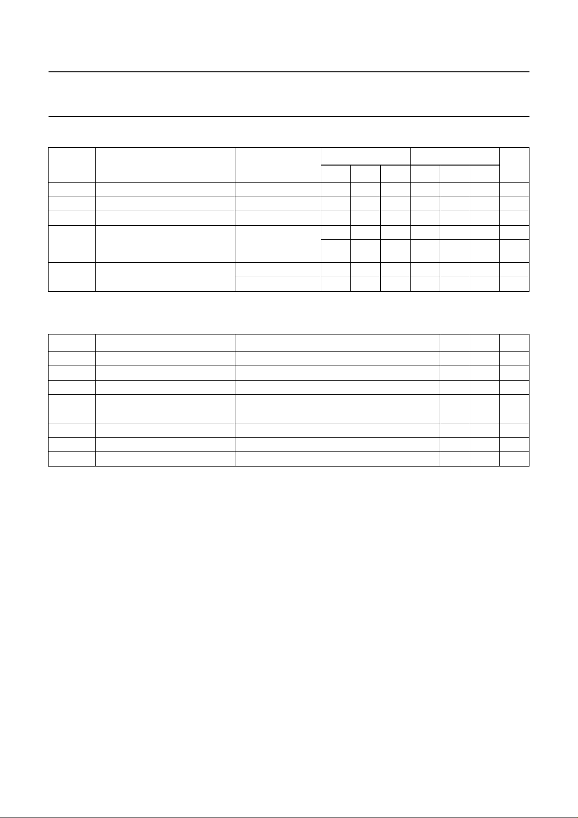
SYMBOL PARAMETER CONDITIONS
t
PHL/tPLH
C
I
C
O
C
PD
propagation delay
Dnto Qn; LE to Q
n
input capacitance VI=VCCor GND 3.0 3.0 pF
output capacitance 4.0 4.0 pF
power dissipation
capacitance
CL= 15 pF; VCC= 5 V 4.3 4.3 ns
CL= 50 pF; f = 1 MHz;
notes 1 and 2
Notes
1. C
is used to determine the dynamic power dissipation (PDin µW).
PD
P
D=CPD
× V
2
× fi+ ∑ (CL× V
CC
2
× fo) where:
CC
fi= input frequency in MHz;
fo= output frequency in MHz;
∑ (CL× V
2
× fo) = sum of outputs;
CC
CL= output load capacitance in pF;
VCC= supply voltage in Volts.
2. The condition is VI= GND to VCC.
TYPICAL
UNIT
AHC AHCT
10 12 pF
1999 Nov 23 2
Philips Semiconductors Product specification
Octal D-type transparent latch; 3-state 74AHC373; 74AHCT373
FUNCTION TABLE
See note 1.
OPERATING MODES
Enable and read register
(transparent mode)
INPUTS
OE LE D
n
INTERNAL
LATCHES
LHLLL
LHHHH
OUTPUTS
Q0to Q
Latch and read register L L I L L
LLhHH
Latch register and
disable outputs
HXXXZ
HXXXZ
Note
1. H = HIGH voltage level;
h = HIGH voltage level one set-up time prior to the HIGH-to-LOW LE transition;
L = LOW voltage level;
I = LOW voltage level one set-up time prior to the HIGH-to-LOW LE transition;
X = don’t care;
Z = high-impedance OFF-state.
ORDERING INFORMATION
OUTSIDE NORTH
AMERICA
NORTH AMERICA
PINS PACKAGE MATERIAL CODE
PACKAGES
74AHC373D 74AHC373D 20 SO plastic SOT163-1
74AHC373PW 74AHC373PW DH 20 TSSOP plastic SOT360-1
74AHCT373D 74AHCT373D 20 SO plastic SOT163-1
74AHCT373PW 7AHCT373PW DH 20 TSSOP plastic SOT360-1
7
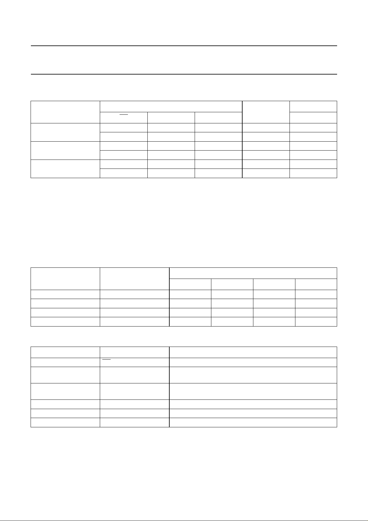
PINNING
PIN SYMBOL DESCRIPTION
1
2, 5, 6, 9, 12, 15, 16
OE output enable input (active LOW)
Q
0
to Q
7
latch outputs
and 19
3, 4, 7, 8, 13, 14, 17
D
0
to D
7
data inputs
and 18
10 GND ground (0 V)
11 LE latch enable input (active HIGH)
20 V
CC
DC supply voltage
1999 Nov 23 3
Philips Semiconductors Product specification
Octal D-type transparent latch; 3-state 74AHC373; 74AHCT373
handbook, halfpage
OE
Q
D
D
Q
Q
D
D
Q
GND
1
2
0
3
0
4
1
5
1
2
2
3
3
373
6
7
8
9
10
20
19
18
17
16
15
14
13
12
11
MNA185
Fig.1 Pin configuration.
V
Q
D
D
Q
Q
D
D
Q
LE
CC
7
7
6
6
5
5
4
4
handbook, halfpage
11
3
4
7
8
13
14
17
18
LE
D
D
D
D
D
D
D
D
Q
0
1
2
3
4
5
6
7
OE
0
Q
1
Q
2
Q
3
12
Q
4
15
Q
5
16
Q
6
19
Q
7
1
MNA186
Fig.2 Logic symbol.
2
5
6
9
handbook, halfpage
1
EN
11
C1
3
1D
4
7
8
13
14
17
18
MNA187
2
5
6
9
12
15
16
19
Fig.3 IEC logic symbol.
1999 Nov 23 4
Philips Semiconductors Product specification
Octal D-type transparent latch; 3-state 74AHC373; 74AHCT373
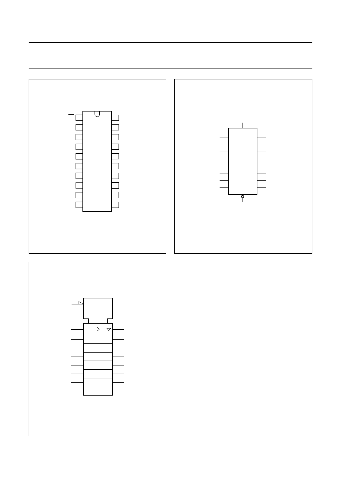
handbook, halfpage
D
3
0
D
1
4
D
7
2
D
8
3
D
13
4
D
14
5
D
17
6
D
18
7
LE
11
OE
1
LATCH
1 to 8
3-STATE
OUTPUTS
Fig.4 Functional diagram.
Q
0
Q
1
Q
2
Q
3
Q
4
Q
5
Q
6
Q
7
MNA184
2
5
6
9
handbook, halfpage
LE
12
15
16
LE
LE
19
D
LE
Q
MNA189
Fig.5 Logic diagram (one latch).
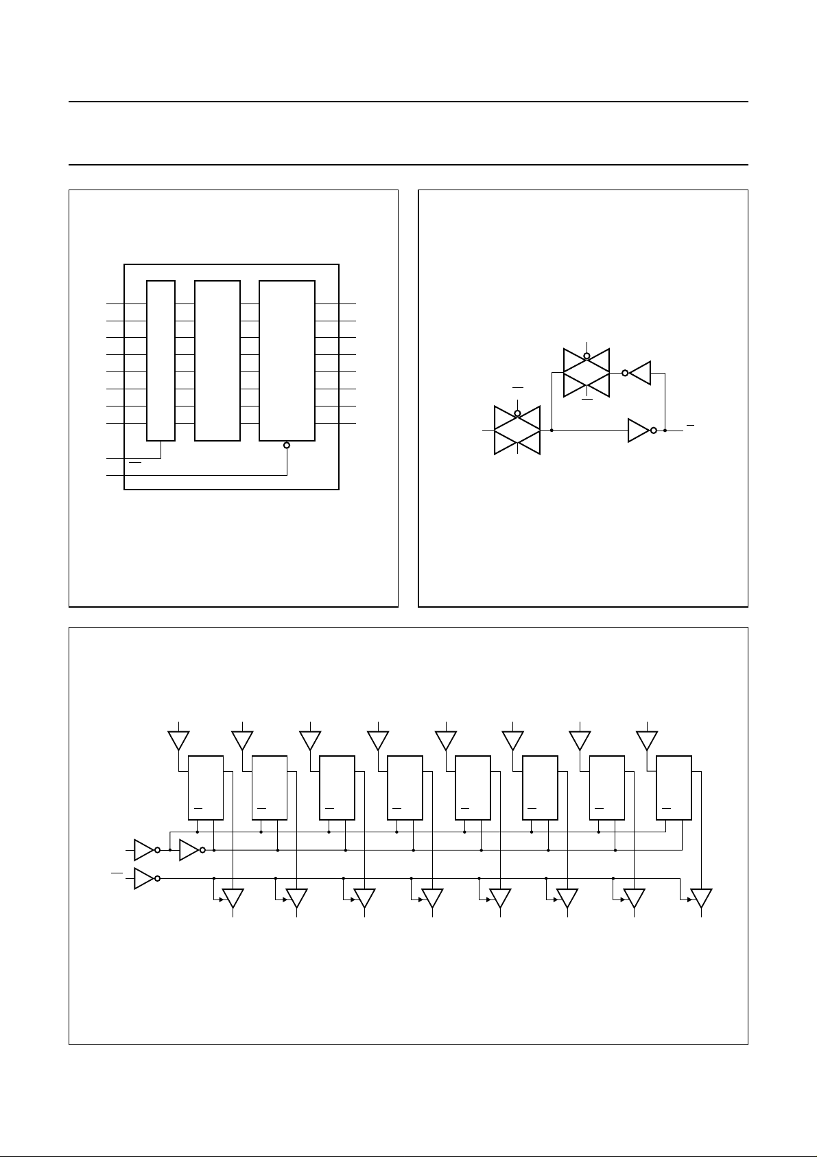
D
3
DLEQ
3
LATCH
Q
2
OE
D
0
D
LATCH
LE
D
1
Q
1
D
LATCH
LE LE LE LE
Q
0
D
2
Q
2
LELELE
DLEQ
LATCH
Q
1
Fig.6 Logic diagram.
1999 Nov 23 5
D
4
DLEQ
4
LATCH
Q
3
D
5
DLEQ
5
LATCH
LE
Q
4
D
6
DLEQ
6
LATCH
LE
Q
5
D
7
DLEQ
7
LATCH
8
LE
Q
6
Q
MNA199
7
handbook, full pagewidth
Philips Semiconductors Product specification
Octal D-type transparent latch; 3-state 74AHC373; 74AHCT373
RECOMMENDED OPERATING CONDITIONS
SYMBOL PARAMETER CONDITIONS
UNIT
MIN. TYP. MAX. MIN. TYP. MAX.
74AHC 74AHCT
V
CC
V
I
V
O
T
amb
DC supply voltage 2.0 5.0 5.5 4.5 5.0 5.5 V
input voltage 0 − 5.5 0 − 5.5 V
output voltage 0 − V
operating ambient temperature see DC and AC
characteristics per
−40 +25 +85 −40 +25 +85 °C
−40 +25 +125 −40 +25 +125 °C
0 − V
CC
CC
V
device
t
(∆t/∆f) input rise and fall rates VCC= 3.3 ±0.3 V −−100 −−−ns/V
r,tf
=5±0.5 V −−20 −−20 ns/V
V
CC
LIMITING VALUES
In accordance with the Absolute Maximum Rating System (IEC 134); voltages are referenced to GND (ground = 0 V).
SYMBOL PARAMETER CONDITIONS MIN. MAX. UNIT
V
CC
V
I
I
IK
I
OK
I
O
I
CC
T
stg
P
D
DC supply voltage −0.5 +7.0 V
input voltage −0.5 +7.0 V
DC input diode current VI< −0.5 V; note 1 −−20 mA
DC output diode current VO< −0.5 Vor VO>VCC+ 0.5 V; note 1 −±20 mA
DC output source or sink current −0.5V<VO<VCC+ 0.5 V −±25 mA
DC VCC or GND current −±75 mA
storage temperature −65 +150 °C
power dissipation per package for temperature range: −40 to +125 °C; note 2 − 500 mW
Notes
1. The input and output voltage ratings may be exceeded if the input and output current ratings are observed.
2. For SO package: above 70 °C the value of P
derates linearly with 8 mW/K.
D
For TSSOP package: above 60 °C the value of PDderates linearly with 5.5 mW/K.
1999 Nov 23 6
 Loading...