

Philips 74AHC138, 74AHCT138 Datasheet

INTEGRATED CIRCUITS
DATA SH EET
74AHC138; 74AHCT138
3-to-8 line decoder/demultiplexer;
inverting
Product specification
Supersedes data of 1999 Mar 31
File under Integrated Circuits, IC06
1999 Sep 27

Philips Semiconductors Product specification
3-to-8 line decoder/demultiplexer; inverting
FEATURES
• ESD protection:
HBM EIA/JESD22-A114-A
exceeds 2000 V
MM EIA/JESD22-A115-A
exceeds 200 V
CDM EIA/JESD22-C101
exceeds 1000 V
• Balanced propagation delays
• All inputs have Schmitt-trigger
actions
• Multiple input enable for easy
expansion
• Ideal for memory chip select
decoding
• Inputs accept voltages higher than
V
CC
• For AHC only:
operates with CMOS input levels
• For AHCT only:
operates with TTL input levels
• Specified from
−40 to +85 and +125 °C.
DESCRIPTION
The 74AHC/AHCT138 are high-speed Si-gate CMOS devices and are pin
compatible with low power Schottky TTL (LSTTL). They are specified in
compliance with JEDEC standard No. 7A.
The 74AHC/AHCT138 decoders accept three binary weighted address inputs
(A0,A1and A2) and when enabled, provide 8 mutually exclusive active LOW
outputs (Y0to Y7).
The ‘138’ features three enable inputs: two active LOW (E1and E2) and one
active HIGH(E3). Every output will be HIGH unless E1and E2are LOW and E
is HIGH.
This multiple enable function allows easy parallel expansion of the ‘138’ to a
1-of-32 (5 to 32 lines) decoder with just four ‘138’ ICs and one inverter.
The ‘138’ can be used as an eight output demultiplexer by using one of the
active LOW enable inputs as the data input and the remaining enable inputs as
strobes. Unused enable inputs must be permanently tied to their appropriate
active HIGH or LOW state.
The ‘138’ is identical to the ‘238’ but has inverting outputs.
74AHC138;
74AHCT138
3
QUICK REFERENCE DATA
GND = 0 V; T
=25°C; tr=tf≤3.0 ns.
amb
SYMBOL PARAMETER CONDITIONS
t
PHL/tPLH
C
I
C
O
C
PD
propagation delay Anto Y
propagation delay E
n
to Yn; Ento YnCL= 15 pF; VCC= 5 V 4.2 4.3 ns
3
input capacitance VI=VCCor GND 3.0 3.0 pF
output capacitance 4.0 4.0 pF
power dissipation capacitance CL= 50 pF; f = 1 MHz;
CL= 15 pF; VCC= 5 V 4.4 4.4 ns
notes 1 and 2
Notes
1. C
is used to determine the dynamic power dissipation (PDin µW).
PD
P
D=CPD
× V
2
× fi+ ∑ (CL× V
CC
2
× fo) where:
CC
fi= input frequency in MHz;
fo= output frequency in MHz;
∑ (CL× V
2
× fo) = sum of outputs;
CC
CL= output load capacitance in pF;
VCC= supply voltage in Volts.
2. The condition is VI= GND to VCC.
TYPICAL
UNIT
AHC AHCT
18 23 pF
1999 Sep 27 2

Philips Semiconductors Product specification
3-to-8 line decoder/demultiplexer; inverting
74AHC138;
74AHCT138
FUNCTION TABLE
See note 1.
INPUT OUTPUT
E
HXXXXXHHHHHHHH
XHXXXXHHHHHHHH
XXLXXXHHHHHHHH
LLHLLLLHHHHHHH
LLHHL LHLHHHHHH
LLHLHLHHLHHHHH
LLHHHLHHHLHHHH
LLHL LHHHHHLHHH
LLHHLHHHHHHLHH
LLHLHHHHHHHHLH
LLHHHHHHHHHHHL
Note
1. H = HIGH voltage level;
L = LOW voltage level;
X = don’t care.
E
1
E
2
A
3
A
0
A
1
Y
2
Y
0
Y
1
Y
2
Y
3
Y
4
Y
5
Y
6
7
ORDERING INFORMATION
OUTSIDE NORTH
AMERICA
NORTH AMERICA
PINS PACKAGE MATERIAL CODE
PACKAGES
74AHC138D 74AHC138D 16 SO plastic SOT109-1
74AHC138PW 74AHC138PW DH 16 TSSOP plastic SOT403-1
74AHCT138D 74AHCT138D 16 SO plastic SOT109-1
74AHCT138PW 74AHCT138PW DH 16 TSSOP plastic SOT403-1
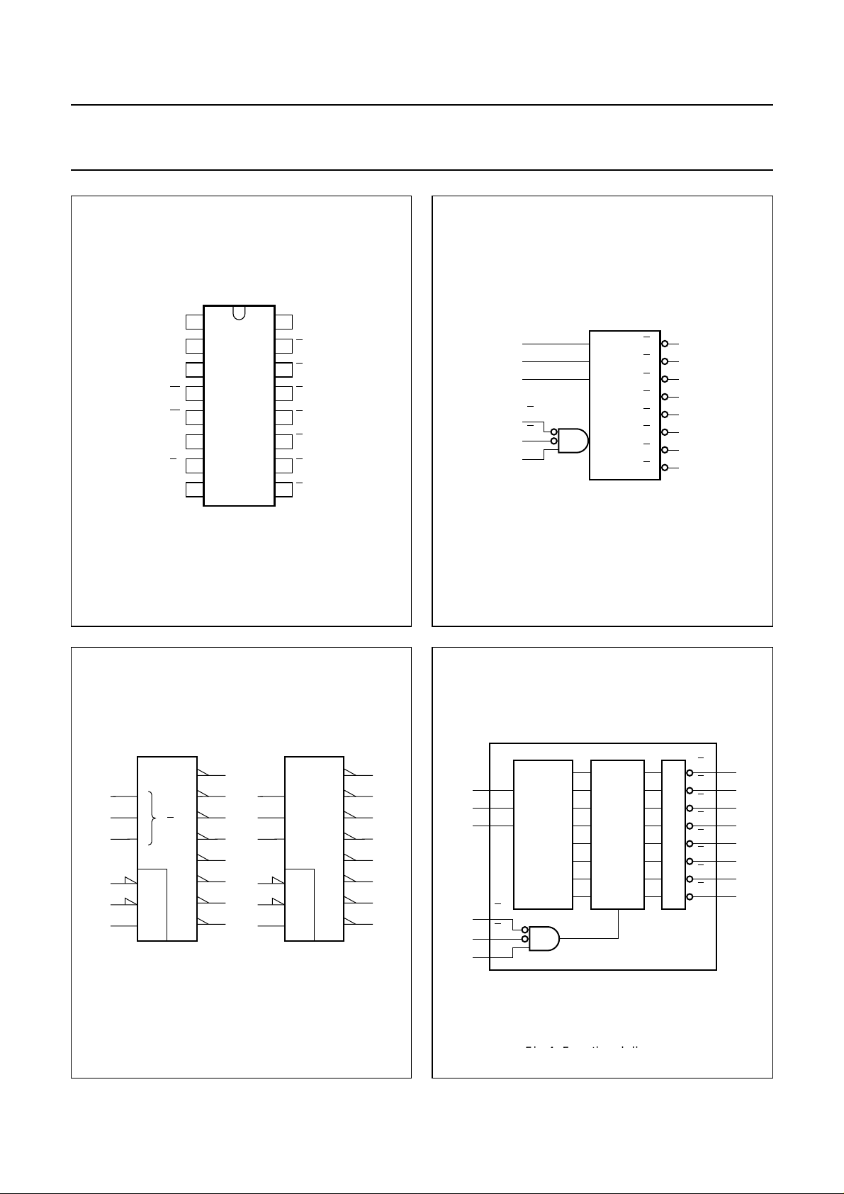
PINNING
PIN SYMBOL DESCRIPTION
1, 2 and 3 A
4 and 5
6E
7, 9, 10 11, 12, 13, 14 and 15
and A2address inputs
0,A1
E1and E
3
Y7to Y
2
0
enable inputs (active LOW)
enable input (active HIGH)
outputs (active LOW)
8 GND ground (0 V)
16 V
CC
DC supply voltage
1999 Sep 27 3
Philips Semiconductors Product specification
3-to-8 line decoder/demultiplexer; inverting
handbook, halfpage
A
A
A
E
E
E
Y
GND
1
0
2
1
3
2
4
1
2
3
7
138
5
6
7
8
MNA369
V
16
CC
Y
15
0
Y
14
1
Y
13
2
Y
12
3
Y
11
4
Y
10
5
Y
9
6
handbook, halfpage
74AHC138;
74AHCT138
Y
1
2
3
E
1
4
E
2
5
E
3
6
0
A
1
A
2
MNA370
15A
0
Y
14
1
13
Y
2
12
Y
3
11
Y
4
10
Y
5
9
Y
6
7
Y
7
handbook, halfpage
1
2
3
4
5
6
Fig.1 Pin configuration.
DX
0
0
G
7
2
&
(a) (b)
15
0
14
1
13
2
12
3
11
4
10
5
9
6
7
7
1
2
3
4
5
6
Fig.2 Logic symbol.
handbook, halfpage
X/Y
1
2
4
&
MNA371
EN
15
0
14
1
13
2
12
3
11
4
10
5
9
6
7
7
A
0
1
A
2
1
A
3
2
3-to-8
DECODER
E
4
1
E
5
2
E
6
3
ENABLE
EXITING
Y
0
Y
1
Y
2
Y
3
Y
4
Y
5
Y
6
Y
7
MNA372
15
14
13
12
11
10
9
7
Fig.3 IEC logic symbol.
1999 Sep 27 4
Fig.4 Functional diagram.
Fig.4 Functional diagram.

Philips Semiconductors Product specification
3-to-8 line decoder/demultiplexer; inverting
74AHC138;
74AHCT138
RECOMMENDED OPERATING CONDITIONS
SYMBOL PARAMETER CONDITIONS
V
CC
V
I
V
O
T
amb
DC supply voltage 2.0 5.0 5.5 4.5 5.0 5.5 V
input voltage 0 − 5.5 0 − 5.5 V
output voltage 0 − V
operating ambient temperature
range
see DC and AC
characteristics per
device
t
(∆t/∆f) input rise and fall rates VCC= 3.3 V ±0.3 V −−100 −−−ns/V
r,tf
=5V±0.5 V −−20 −−20
V
CC
LIMITING VALUES
In accordance with the Absolute Maximum Rating System (IEC 134); voltages are referenced to GND (ground= 0 V).
SYMBOL PARAMETER CONDITIONS MIN. MAX. UNIT
V
CC
V
I
I
IK
I
OK
I
O
I
CC
T
stg
P
D
DC supply voltage −0.5 +7.0 V
input voltage range −0.5 +7.0 V
DC input diode current VI< −0.5 V; note 1 −−20 mA
DC output diode current VO< −0.5 Vor VO>VCC+ 0.5 V; note 1 −±20 mA
DC output source or sink current −0.5V<VO<VCC+ 0.5 V −±25 mA
DC VCC or GND current −±75 mA
storage temperature range −65 +150 °C
power dissipation per package for temperature range: −40 to +125 °C; note 2 − 500 mW
74AHC 74AHCT
UNIT
MIN. TYP. MAX. MIN. TYP. MAX.
0 − V
CC
CC
V
−40 +25 +85 −40 +25 +85 °C
−40 +25 +125 −40 +25 +125 °C
Notes
1. The input and output voltage ratings may be exceeded if the input and output current ratings are observed.
2. For SO packages: above 70 °C the value of P
derates linearly with 8 mW/K.
D
For TSSOP packages: above 60 °C the value of PDderates linearly with 5.5 mW/K.
1999 Sep 27 5
 Loading...