

Philips 74AHC132, 74AHCT132 Datasheet

INTEGRATED CIRCUITS
DATA SH EET
74AHC132; 74AHCT132
Quad 2-input NAND Schmitt trigger
Product specification
Supersedes data of 1999 May 31
File under Integrated Circuits, IC06
1999 Sep 24
Philips Semiconductors Product specification
Quad 2-input NAND Schmitt trigger 74AHC132; 74AHCT132
FEATURES
• ESD protection:
HBM EIA/JESD22-A114-A
exceeds 2000 V;
MM EIA/JESD22-A115-A
exceeds 200 V
CDM EIA/JESD22-C101
exceeds 1000 V
• Balanced propagation delays
• Inputsacceptsvoltageshigherthan
V
CC
• For AHC only:
operates with CMOS input levels
• For AHCT only:
operates with TTL input levels
• Specified from
−40 to +85 and +125 °C.
DESCRIPTION
The 74AHC/AHCT132 are
high-speed Si-gate CMOS devices
and are pin compatible with Low
power Schottky TTL (LSTTL). They
are specified in compliance with
JEDEC standard No. 7A.
The 74AHC/AHCT132 contain four
2-input NAND gates which accept
standard input signals. They are
capable of transforming slowly
changing input signals into sharply
defined, jitter free output signals.
The gate switches at different points
for positive and negative-going
signals. The difference between the
positive voltage VT+and the negative
VT− is defined as the hysteresis
voltage VH.
FUNCTION TABLE
See note 1.
INPUTS OUTPUT
nA nB nY
LLH
LHH
HLH
HHL
Note
1. H = HIGH voltage level; L = LOW voltage level.
QUICK REFERENCE DATA
GND = 0 V; T
=25°C; tr=tf≤3.0 ns.
amb
SYMBOL PARAMETER CONDITIONS
t
PHL/tPLH
C
I
C
O
C
PD
propagation delay
nA to nY
input capacitance VI=VCCor GND 3.0 3.0 pF
output capacitance 4.0 4.0 pF
power dissipation
capacitance
CL= 15 pF;
VCC=5V
CL= 50 pF;
f = 1 MHz;
notes 1 and 2
Notes
1. C
is used to determine the dynamic power dissipation (PDin µW).
PD
PD=CPD× V
2
× fi+ ∑ (CL× V
CC
2
× fo) where:
CC
fi= input frequency in MHz;
fo= output frequency in MHz;
∑ (CL× V
2
× fo) = sum of outputs;
CC
CL= output load capacitance in pF;
VCC= supply voltage in Volts.
2. The condition is VI= GND to VCC.
TYPICAL
UNIT
AHC AHCT
3.3 3.5 ns
11 14 pF
ORDERING INFORMATION
OUTSIDE NORTH
AMERICA
NORTH AMERICA
PINS PACKAGE MATERIAL CODE
PACKAGES
74AHC132D 74AHC132D 14 SO plastic SOT108-1
74AHC132PW 74AHC132PW DH 14 TSSOP plastic SOT402-1
74AHCT132D 74AHCT132D 14 SO plastic SOT108-1
74AHCT132PW 74AHCT132PW DH 14 TSSOP plastic SOT402-1
1999 Sep 24 2
Philips Semiconductors Product specification
Quad 2-input NAND Schmitt trigger 74AHC132; 74AHCT132
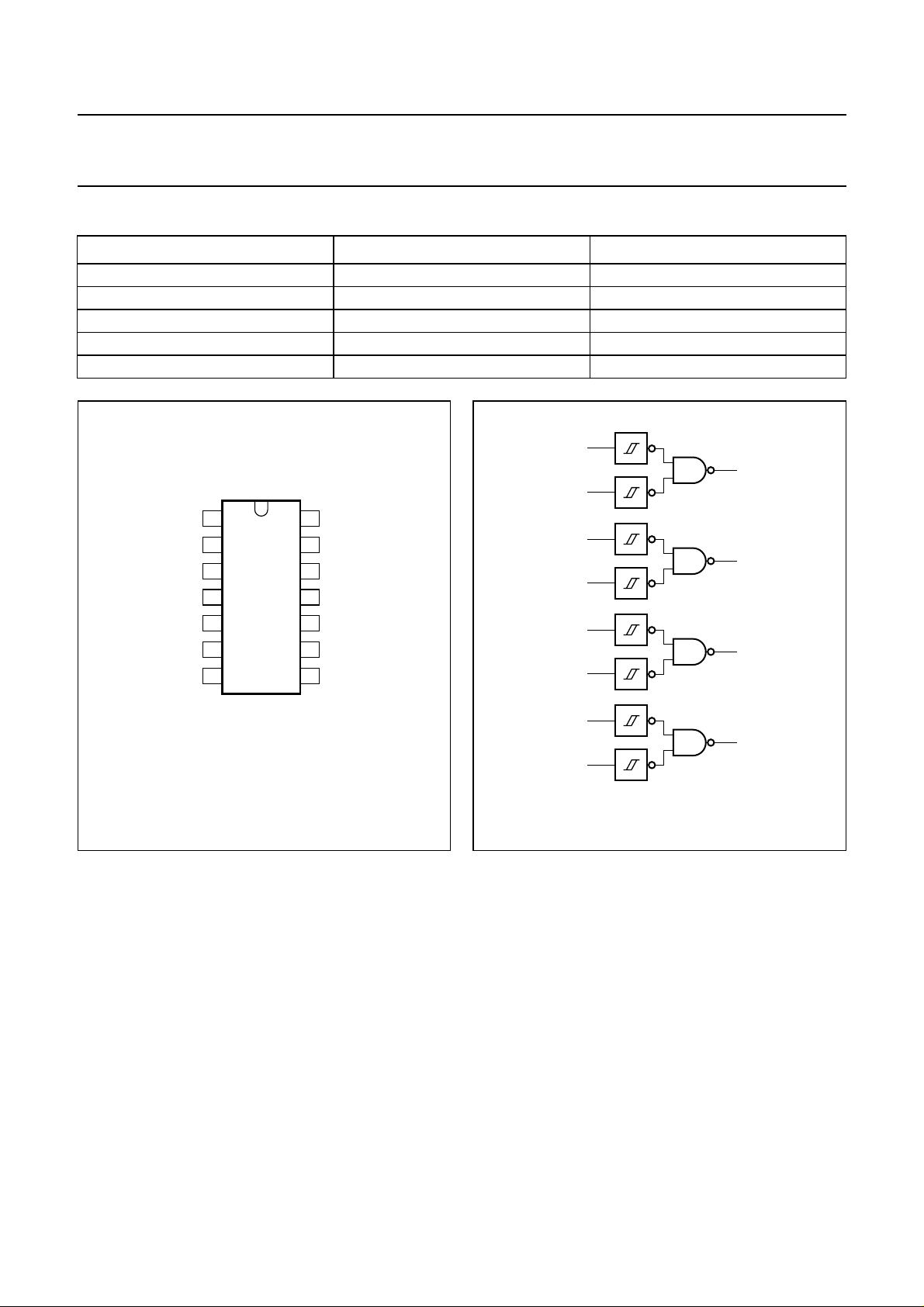
PINNING
PIN SYMBOL DESCRIPTION
1, 4, 9 and 12 1A to 4A data inputs
2, 5, 10 and 13 1B to 4B data inputs
3, 6, 8 and 11 1Y to 4Y data outputs
7 GND ground (0 V)
14 V
CC
DC supply voltage
handbook, halfpage
1A
1
1B
2
3
1Y
4
2A
2B
2Y
GND
132
5
6
7
MNA406
Fig.1 Pin configuration.
handbook, halfpage
V
14
CC
13
4B
12
4A
11
4Y
10
3B
9
3A
8
3Y
1A
1
1Y
2Y
3Y
4Y
MNA407
3
6
8
11
1B
2
2A
4
2B
5
3A
9
3B
10
4A
12
4B
13
Fig.2 Logic symbol.
1999 Sep 24 3
Philips Semiconductors Product specification
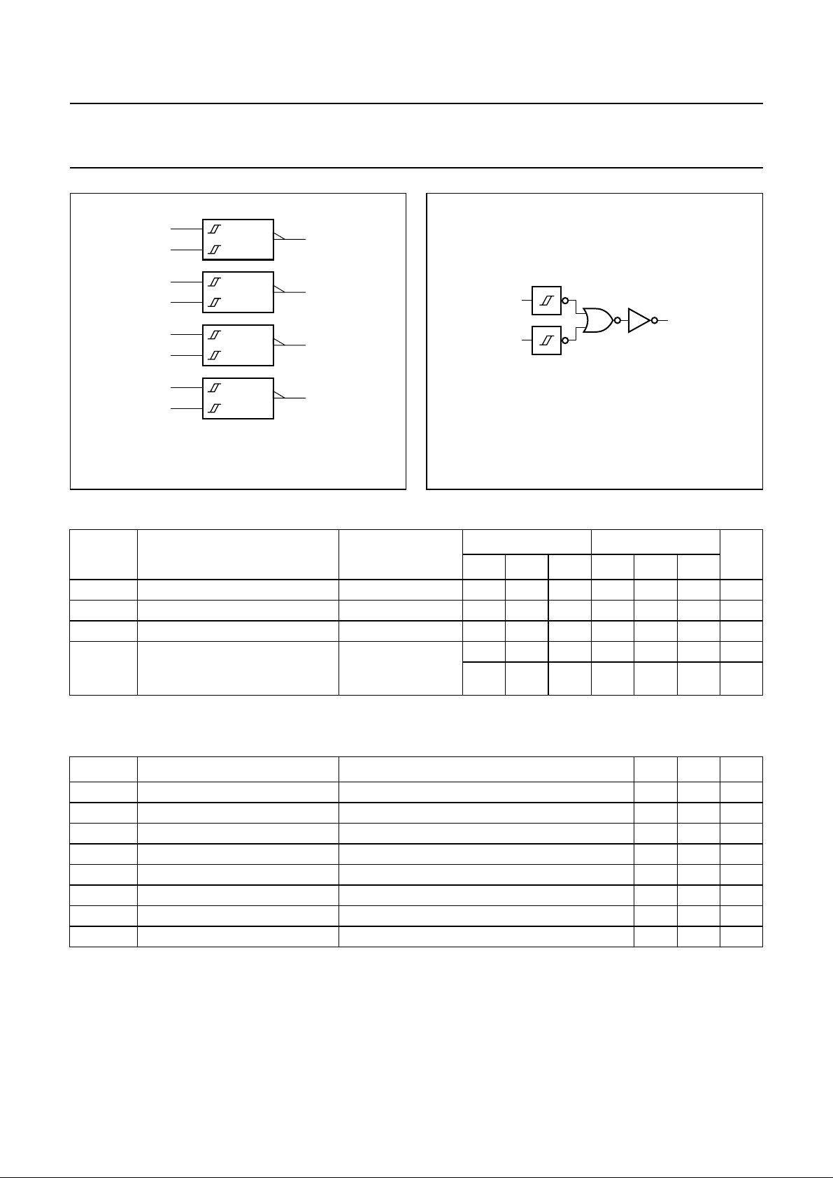
Quad 2-input NAND Schmitt trigger 74AHC132; 74AHCT132
handbook, halfpage
1
2
4
5
9
10
12
13
&
&
&
&
3
6
8
11
MNA408
Fig.3 IEC logic symbol.
RECOMMENDED OPERATING CONDITIONS
SYMBOL PARAMETER CONDITIONS
V
CC
V
I
V
O
T
amb
DC supply voltage 2.0 5.0 5.5 4.5 5.0 5.5 V
input voltage 0 − 5.5 0 − 5.5 V
output voltage 0 − V
operating ambient temperature
range
see DC and AC
characteristics per
device
handbook, halfpage
A
B
MNA409
Fig.4 Logic diagram (one Schmitt trigger).
74AHC 74AHCT
MIN. TYP. MAX. MIN. TYP. MAX.
0 − V
CC
−40 +25 +85 −40 +25 +85 °C
−40 +25 +125 −40 +25 +125 °C
Y
UNIT
V
CC
LIMITING VALUES
In accordance with the Absolute Maximum Rating System (IEC 134); voltages are referenced to GND (ground= 0 V).
SYMBOL PARAMETER CONDITIONS MIN. MAX. UNIT
V
CC
V
I
I
IK
I
OK
I
O
I
CC
T
stg
P
D
DC voltage −0.5 +7.0 V
input voltage range −0.5 +7.0 V
DC input diode current VI< −0.5 V; note 1 −−20 mA
DC output diode current VO< −0.5 Vor VO>VCC+ 0.5 V; note 1 −±20 mA
DC output source or sink current −0.5V<VO<VCC+ 0.5 V −±25 mA
DC VCC or GND current −±75 mA
storage temperature range −65 +150 °C
power dissipation per package for temperature range: −40 to +125 °C; note 2 − 500 mW
Notes
1. The input and output voltage ratings may be exceeded if the input and output current ratings are observed.
2. For SO packages: above 70 °C the value of P
derates linearly with 8 mW/K.
D
For TSSOP packages: above 60 °C the value of PDderates linearly with 5.5 mW/K.
1999 Sep 24 4
Philips Semiconductors Product specification
Quad 2-input NAND Schmitt trigger 74AHC132; 74AHCT132
DC CHARACTERISTICS
Type 74AHC132
Over recommended operating conditions; voltage are referenced to GND (ground = 0 V).
SYMBOL PARAMETER
V
T+
positive going
threshold
V
T−
negative going
threshold
V
H
hysteresis
(VT+− VT−)
V
OH
HIGH-level output
voltage; all
outputs
HIGH-level output
voltage
V
OL
LOW-level output
voltage; all
outputs
LOW-level output
voltage
I
I
input leakage
current
I
CC
quiescent supply
current
C
I
input capacitance − 310−10 − 10 pF
TEST CONDITIONS T
25 −40 to +85 −40 to +125
amb
(°C)
UNIT
OTHER VCC(V)
MIN. TYP. MAX. MIN. MAX. MIN. MAX.
3.0 −− 2.2 − 2.2 − 2.2 V
4.5 −− 3.15 − 3.15 − 3.15
5.5 −− 3.85 − 3.85 − 3.85
3.0 0.9 −−0.9 − 0.9 − V
4.5 1.35 −−1.35 − 1.35 −
5.5 1.65 −−1.65 − 1.65 −
3.0 0.3 − 1.2 0.3 1.2 0.25 1.2 V
4.5 0.4 − 1.4 0.4 1.4 0.35 1.4
5.5 0.5 − 1.6 0.5 1.6 0.45 1.6
VI=VIHor VIL;
IO= −50 µA
2.0 1.9 2.0 − 1.9 − 1.9 − V
3.0 2.9 3.0 − 2.9 − 2.9 −
4.5 4.4 4.5 − 4.4 − 4.4 −
V
I=VIH
or VIL;
3.0 2.58 −−2.48 − 2.40 − V
IO= −4.0 mA
V
I=VIH
or VIL;
4.5 3.94 −−3.8 − 3.7 −
IO= −8.0 mA
VI=VIHor VIL;
IO=50µA
2.0 − 0 0.1 − 0.1 − 0.1 V
3.0 − 0 0.1 − 0.1 − 0.1
4.5 − 0 0.1 − 0.1 − 0.1
V
I=VIH
or VIL;
3.0 −− 0.36 − 0.44 − 0.55 V
IO=4mA
V
I=VIH
or VIL;
4.5 −− 0.36 − 0.44 − 0.55
IO=8mA
VI=VCCor GND 5.5 −− 0.1 − 1.0 − 2.0 µA
VI=VCCor GND;
5.5 −− 2.0 − 20 − 40 µA
IO=0
1999 Sep 24 5
 Loading...