

Philips 74ABTL3205BB Datasheet

INTEGRATED CIRCUITS
74ABTL3205
10-bit BTL transceiver with registers
Product specification 1995 Jun 16
Philips Semiconductors Product specification
ns
ns
74ABTL320510-bit BTL transceiver with registers
FEA TURES
•10-bit BTL transceiver
•Drives heavily loaded backplanes with equivalent load
impedances down to 10 ohms
•High drive 100mA BTL open collector drivers on B-port
•Allows incident wave switching in heavily loaded backplane buses
•Reduced BTL voltage swing produces less noise and reduces
power consumption
•Built-in precision band-gap reference provides accurate receiver
thresholds and improved noise immunity
•Compatible with IEEE Futurebus+ or proprietary BTL backplanes
•Controlled output ramp and multiple GND pins minimize ground
bounce
•Tight output skew (0.5nsec typical)
•Glitch-free power up/down operation
•Low I
current
CC
•Supports live insertion
•High density packaging
•ESD protection exceeds 2000V per MIL STD 883 Method 3015
and 200V per Machine Model
DESCRIPTION
This transceiver is a 10 bit bidirectional transceiver and is intended
to provide the electrical interface to a high performance wired-OR
bus.
The B-port drivers are Low-capacitance open collectors with
controlled ramp and are designed to sink 100mA. Precision band
gap references on the B-port insure very good margins by limiting
the switching threshold to a narrow region centered at 1.55V .
The B-port interfaces to “Backplane Transceiver Logic” (See the
IEEE 1194.1 BTL standard). BTL features low power consumption
by reducing voltage swing (1V p-p, between 1V and 2V) and
reduced capacitive loading (<6pF) by placing an internal series
diode on the drivers. BTL also provides incident wave switching, a
necessity for high performance backplanes.
To support live insertion, OEB is held Low during power on/off cycles
to insure glitch free B port drivers. Proper bias for B port drivers
during live insertion is provided by the BIAS V pin when at a 5V level
while V
reverse bias the BTL driver series Schottky diode, and also bias the
B port output pins to a voltage between 1.62V and 2.1V . This bias
function is in accordance with IEEE BTL standard 1194.1. If live
insertion is not a requirement, the BIAS V pin should be tied to a
V
The LOGIC GND and BUS GND pins are isolated inside the
package to minimize noise coupling between the BTL and TTL
sides. These pins should be tied to a common ground external to the
package. The LOGIC V
internally to minimize noise and may be externally decoupled
separately or simply tied together.
This transceiver function is intended to operate in a half-duplex
mode. Low current in standby mode is obtained by powering down
unused circuitry. Likewise, transmit circuitry is powered down when
in receive mode and receive circuitry is powered down while in
transmit mode.
is Low. The BIAS V pin is a low current input which will
CC
pin.
CC
and BUS VCC pins are also isolated
CC
QUICK REFERENCE DATA
SYMBOL PARAMETER TYPICAL UNIT
t
PLH
t
PHL
t
PLH
t
PHL
C
I
I
OB
OL
CC
Propagation delay 3.3
An to Bn 3.7
Propagation delay 3.6
Bn to An 3.5
Output capacitance (B0 - B8) only) 6 pF
Output current (B0 - B8) only) 100 mA
Standby 1
Supply current
An to Bn 7
Bn to An 18
mA
ORDERING INFORMATION
PACKAGES TEMPERATURE RANGE OUTSIDE NORTH AMERICA NORTH AMERICA DWG NUMBER
52-PIN PQFP –40°C to +85°C 74ABTL3205 BB 74ABTL3205 BB SOT379-1
1995 Jun 16 853-1802 15352
2

Philips Semiconductors Product specification
74ABTL320510-bit BTL transceiver with registers
PIN CONFIGURATION
TTL Gnd
TTL GND
TTL GND
AClk2
TTL GND
TTL GND
CC
AClkin
TTL Gnd
AClk1
1
2
A0
A1
3
4
A2
5
6
A3
7
8
9
A4
10
A5
11
12
A6
13
14 15 16 17 18 19 20
A7
TTL Gnd
V
CC
BG V
49505152
APAR
BG GND
BiasV
OEA1
OEA2
464748
21 22 23 24 25 26
AFP
Power Up
OEB
M/S
Mode
IEA
Recmode
V
434445 404142
CC
V
Transmode
CC
BUS GND
BUS GND
BClk1
B7
39
38
37
36
35
34
33
32
31
30
29
28
27
BUS GND
B0
B1
BUS GND
B2
B3
BUS GND
BClk2
BUS GND
B4
B5
BUS GND
B6
SA00138
PIN DESCRIPTION
SYMBOL FUNCTION ASSERTION I/O LOGIC
OEA1 Output enable data receiver group 1 Low Input TTL
OEA2 Output enable data receiver group 2 Low Input TTL
OEB Output enable data transmitter Low Input TTL
IEA Output enable clock and framepulse receiver Low Input TTL
M/S Master/Slave select:
L: Master, enable clock transmitter
H: Slave, disable clock transmitter
Mode
Low: Data through mode
High: Registered data mode
Power Up Power up mode, held low during power up to
Low Input TTL
disable clock and data transmitters
Recmode Enables receiver High Input TTL
Tranmode Enables transmitter High Input TTL
AClk1 Clock or data path I/O TTL
AClkln
IEA = H → Input for busclock
IEA = L → Output for busclock
A0..A3 data group 1 I/O TTL
AClk2 Clock or data path I/O TTL
AFPIn Alternate data path Output TTL
APAR Alternate data path Input TTL
A4..A7 data group 2 I/O TTL
BClk1 Clock or data path I/O BTL
B0..B3 data group 1 I/O BTL
BClk2 Clock or data path I/O BTL
B4..B7 data group 2 I/O BTL
Input TTL
Input TTL
I/O TTL
1995 Jun 16
3
Philips Semiconductors Product specification
74ABTL320510-bit BTL transceiver with registers
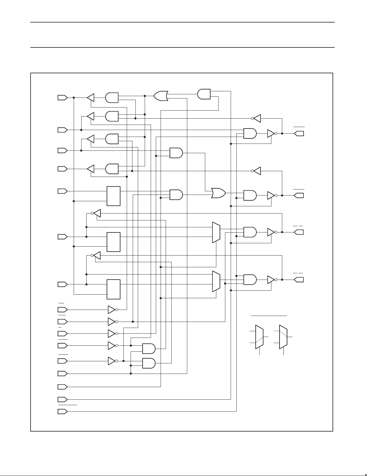
LOGIC DIAGRAM
ACLKin
I/O
OUT
I/O
I/O
IN
I/O
I/O
ACLK1
ACLK2
AFP
APAR
A0-A3
A4-A7
DCQ
DCQ
DCQ
BCLK1
BCLK2
B0-B3
B4
-B7
I/O
I/O
I/O
I/O
IN
IN
IN
IN
IN
IN
IN
IN
IN
1995 Jun 16
IEA
OEB
/S
M
OEA1
OEA2
RECMODE
MODE
TRANMODE
POWERUP
Definition for the MUX:
Low High
SA00139
4

Philips Semiconductors Product specification
to
to
to
to
to
to
to
to
to
to
to
to
to
to
74ABTL320510-bit BTL transceiver with registers
FUNCTION TABLE
MODE
An to Bn
(REGISTERED)
AN to Bn
(THROUGH)
B0-B3
to
A0-A3
(THROUGH)
B4-B7
to
A4-A7
(THROUGH)
ACLK1
BCLK1
ACLK2
BCLK2
BCLK1
ACLK1
BCLK2
ACLK2
APAR
BCLK2
BCLK2
AFPIn
BCLK1
ACLKin
An Bn
I O ° X X X X H H L X H X H L H H
h O ° X X X X H H L X H X H L H H
L O X X X X X H H L X X X L L H H
H O X X X X X H H L X X X L L H H
O L X X X X X L X H X X X X H L L
O H X X X X X L X H X X X X H L L
O L X X X X X X L H X X X X H L L
O H X X X X X X L H X X X X H L L
X X X L X O X H X X X X L X X H H
X X X H X O X H X X X X L X X H H
X X X X L X O X H H X X L L X H H
X X X X H X O X H H X X L L X H H
X X X O X L X L X X X X X X H L X
X X X O X H X L X X X X X X H L X
X X X X O X L X L X X X X X H L X
X X X X O X H X L X X X X X H L X
X X ° X X X X X X L I X H H X H H
X X ° X X X X X X L h X H H X H H
X X X X X X L X X X X L X X H L X
X X X X X X H X X X X L X X H L X
X X O X X L X H H L O L H H L H H
X X O X X H X H H L O L H H L H H
ACLKinACLK1ACLK2BCLK1BCLK
2
OEA1 OEA2 OEB APAR IEA M/S MODE
INPUTS
REC
MODE
TRAN
MODE
POWER
UP
MODE
An to Bn
(REGISTERED)
AN to Bn
(THROUGH)
B0-B3
to
A0-A3
(THROUGH)
B4-B7
to
A4-A7
(THROUGH)
ACLK1
BCLK1
ACLK2
BCLK2
BCLK1
ACLK1
BCLK2
ACLK2
APAR
BCLK2
BCLK2
AFPIn
BCLK1
ACLKin
OUTPUTS
An Bn
Input H* X X X X X X
Input L X X X X X X
Input H* X X X X X X
Input L X X X X X X
H Input Input X X X X X
L Input Input X X X X X
H Input Input X X X X X
L Input Input X X X X X
X X X Input X H* X X
X X X Input X L X X
X X X X Input X H* X
X X X X Input X L X
X X X H X Input X X
X X X L X Input X X
X X X X H X Input X
X X X X L X Input X
X X Input X X X H* X
X X Input X X X L X
X X X X X X Input H*
X X X X X X Input L
X X H X X Input X X
X X L X X Input X X
ACLK
ACLK1 ACLK2 BCLK1 BCLK2
in
AF
Pin
NOTES:
H = High voltage level
L = Low voltage level
h = High voltage level one set-up time prior to
Low to High ACLKin transition
l = Low voltage level one set-up time prior to
Low to High ACLKin transition
° = Low to High transition
Z = High impedance (off) state
H* = Goes to level of pull-up voltage
X = Don’t care
O = Output
1995 Jun 16
5
 Loading...