Philips 74ABT16825A, 74ABTH16825A Technical data

Philips 74ABT16825A, 74ABTH16825A Technical data


74ABT16825A

INTEGRATED CIRCUITS


74ABT16825A

74ABTH16825A

18-bit buffer/line driver; non-inverting

(3-State)

Product specification

1998 Feb 25

Supersedes data of 1995 Jul 14

IC23 Data Handbook

m n r

Philips Semiconductors

Product specification


18-bit buffer/line driver; non-inverting (3-State)

74ABT16825A

74ABTH16825A


FEATURES

Multiple VCC and GND pins minimize switching noise

Live insertion/extraction permitted

3-State output buffers

Power-up 3-State

74ABTH16825A incorporates bus-hold data inputs which eliminate the need for external pull-up resistors to hold unused inputs

Output capability: +64mA/±32mA

Latch-up protection exceeds 500mA per Jedec Std 17

ESD protection exceeds 2000V per MIL STD 883 Method 3015 and 200V per Machine Model

Bus-hold data inputs eliminate the need for external pull-up resistors to hold unused inputs

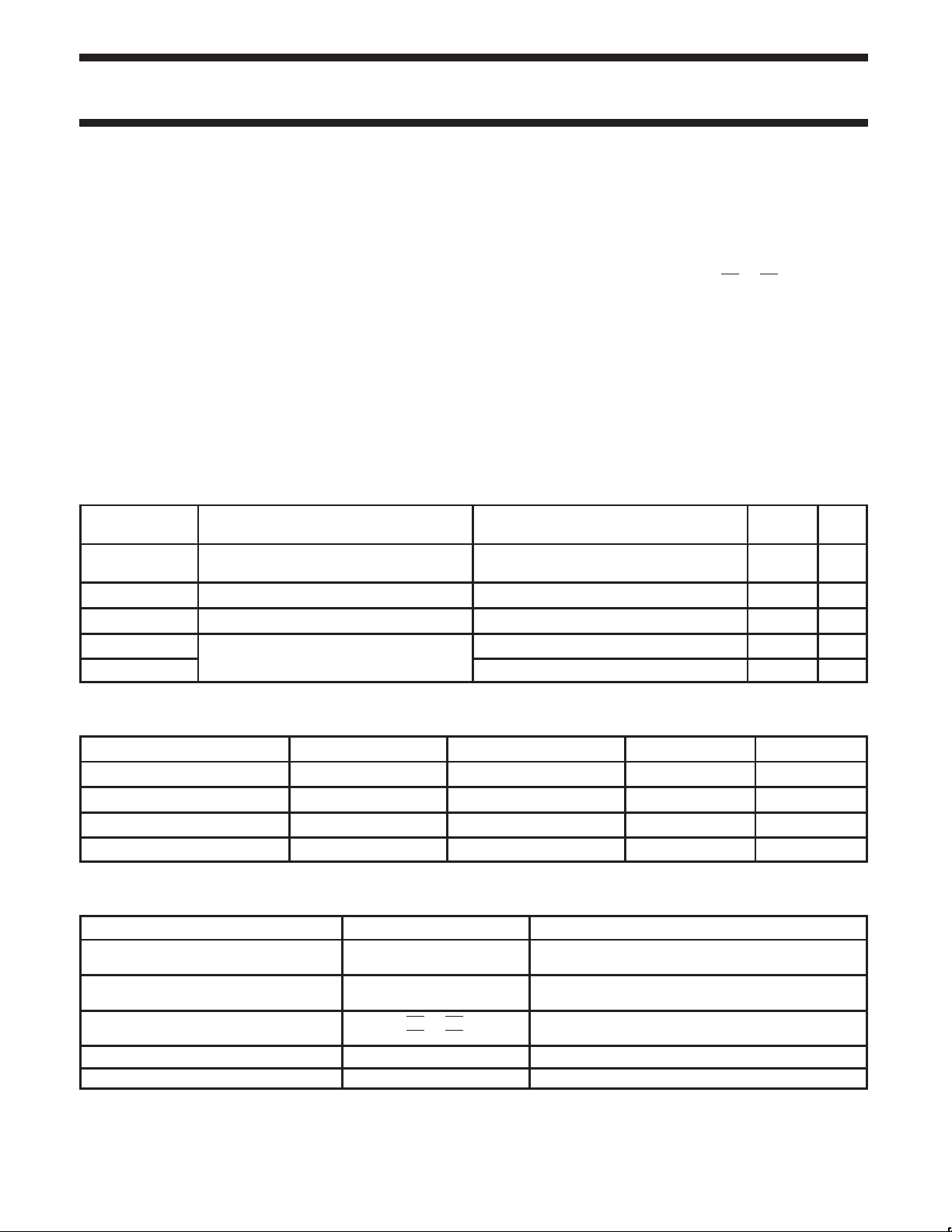
QUICK REFERENCE DATA

DESCRIPTION

The74ABT16825A high-performance BiCMOS device combines low static and dynamic power dissipation with high speed and high output drive.

The74ABT16825A 18-bit buffers provide high performance bus interface buffering for wide data/address paths or buses carrying parity. They have NOR Output Enables (nOE1, nOE2) for maximum control flexibility.

Two options are available, 74ABT16825A which does not have the bus-hold feature and 74ABTH16825A which incorporates the bus-hold feature.

SYMBOL

PARAMETER

CONDITIONS

TYPICAL

UNIT

Tamb = 25°C; GND = 0V


tPLH

Propagation delay

CL = 50pF; VCC = 5V

1.8

ns

tPHL

nAx to nYx

1.4


CIN

Input capacitance

VI = 0V or VCC

4

pF

COUT

Output capacitance

VO = 0V or VCC; 3-State

6

pF

ICCZ

Quiescent supply current

Outputs disabled; VCC = 5.5V

500

μA

ICCL

Outputs Low; VCC = 5.5V

9

mA


ORDERING INFORMATION

PACKAGES

TEMPERATURE RANGE

OUTSIDE NORTH AMERICA

NORTH AMERICA

DWG NUMBER


56-pin SSOP Type III

±40°C to +85°C

74ABT16825A DL

BT16825A DL

SOT371-1


56-pin TSSOP Type II

±40°C to +85°C

74ABT16825A DGG

BT16825A DGG

SOT364-1


56-pin SSOP Type III

±40°C to +85°C

74ABTH16825A DL

BH16825A DL

SOT371-1


56-pin TSSOP Type II

±40°C to +85°C

74ABTH16825A DGG

BH16825A DGG

SOT364-1
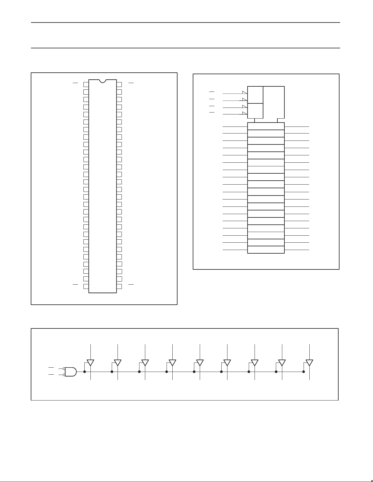


PIN DESCRIPTION

PIN NUMBER


SYMBOL

FUNCTION


55, 54, 52, 51, 49, 48, 47, 45, 44,

1A0 ± 1A9

Data inputs

41, 40, 38, 37, 36, 34, 33, 31, 30

2A0 ± 2A9


2, 3, 5, 6, 8, 9, 10, 12, 13

1Y0 ± 1Y9

Data outputs

16, 17, 19, 20, 21, 23, 24, 26, 27

2Y0 ± 2Y9


1, 56


1OE0, 1OE1

Output enable inputs (active-Low)


28, 29

2OE0, 2OE1


4, 11, 14, 15, 18, 25, 32, 39, 42, 43, 46, 53


GND

Ground (0V)


7, 22, 35, 50


VCC

Positive supply voltage

1998 Feb 25

2

853-1804 19018

Philips Semiconductors

Product specification


18-bit buffer/line driver; non-inverting (3-State)

74ABT16825A

74ABTH16825A


PIN CONFIGURATION


1OE0

1


56

1OE1


1Y0


1A0


2


55


1Y1


1A1


3


54

GND


GND


4


53


1Y2


1A2


5


52


1Y3


1A3


6


51


VCC


7


50

VCC


1Y4


8


49

1A4


1Y5


9


48

1A5


1Y6


10


47

1A6

GND


11


46

GND


1Y7


12


45

1A7


1Y8


13


44

1A8

GND


14


43

GND

GND


15


42

GND


2Y0

16


41

2A0


2Y1


17


40

2A1

GND


18


39

GND


2Y2


19


38

2A2


2Y3


20


37

2A3


2Y4


21


36

2A4


VCC


22


35

VCC


2Y5

23


34

2A5


2Y6


2A6


24


33


GND

GND


25


32


2Y7


26


31

2A7


2Y8


27


30

2A8


2OE0


28


29


2OE1


SA00073

LOGIC SYMBOL (IEEE/IEC)


1


&


1OE0


EN1


56


1OE1


28


&


2OE0


EN2


29


2OE1


55


2


1A0


1

1Y0

54


3


1A1


1Y1


52


5


1A2


1Y2


51


6


1A3


1Y3


49


8


1A4


1Y4


48


9


1A5


1Y5


47


10


1A6


1Y6


45


12


1A7


1Y7


44


13


1A8


1Y8


41


16


2A0


2Y0


2


40


17


2A1


2Y1


38


19


2A2


2Y2


37


20


2A3


2Y3


36


21


2A4


2Y4


34


23


2A5


2Y5


33


24


2A6


2Y6


31


26


2A7


2Y7


30


27


2A8


2Y8


SA00074


LOGIC DIAGRAM

nA0

nA1

nA2

nA3

nA4

nA5

nA6

nA7

nA8

nOE0


nOE1


nY0

nY1

nY2

nY3

nY4

nY5

nY6

nY7

nY8


SA00075

1998 Feb 25

3

Loading...
+ 7 hidden pages