Philips 74ABTH16646DL, 74ABTH16646DGG, 74ABT16646DGG, 74ABT16646DL Datasheet

0 (0)

INTEGRATED CIRCUITS

74ABT16646

74ABTH16646

16-bit bus transceiver/register (3-State)

Product specification

1998 Feb 27

Supersedes data of 1995 Aug 17

IC23 Data Handbook

m n r

Philips Semiconductors

Product specification


16-bit bus transceiver/register (3-State)

74ABT16646

74ABTH16646


FEATURES

Independent registers for A and B buses

Multiple VCC and GND pins minimize switching noise

Live insertion/extraction permitted

Power±up 3-State

Power±up reset

Multiplexed real-time and stored data

Outputs sink 64mA and source 32mA

Latch±up protection exceeds 500mA per JEDEC Std 17

74ABTH16646 incorporates bus-hold data inputs which eliminate the need for external pull-up resistors to hold unused inputs

ESD protection exceeds 2000V per MIL STD 883 Method 3015 and 200V per Machine Model

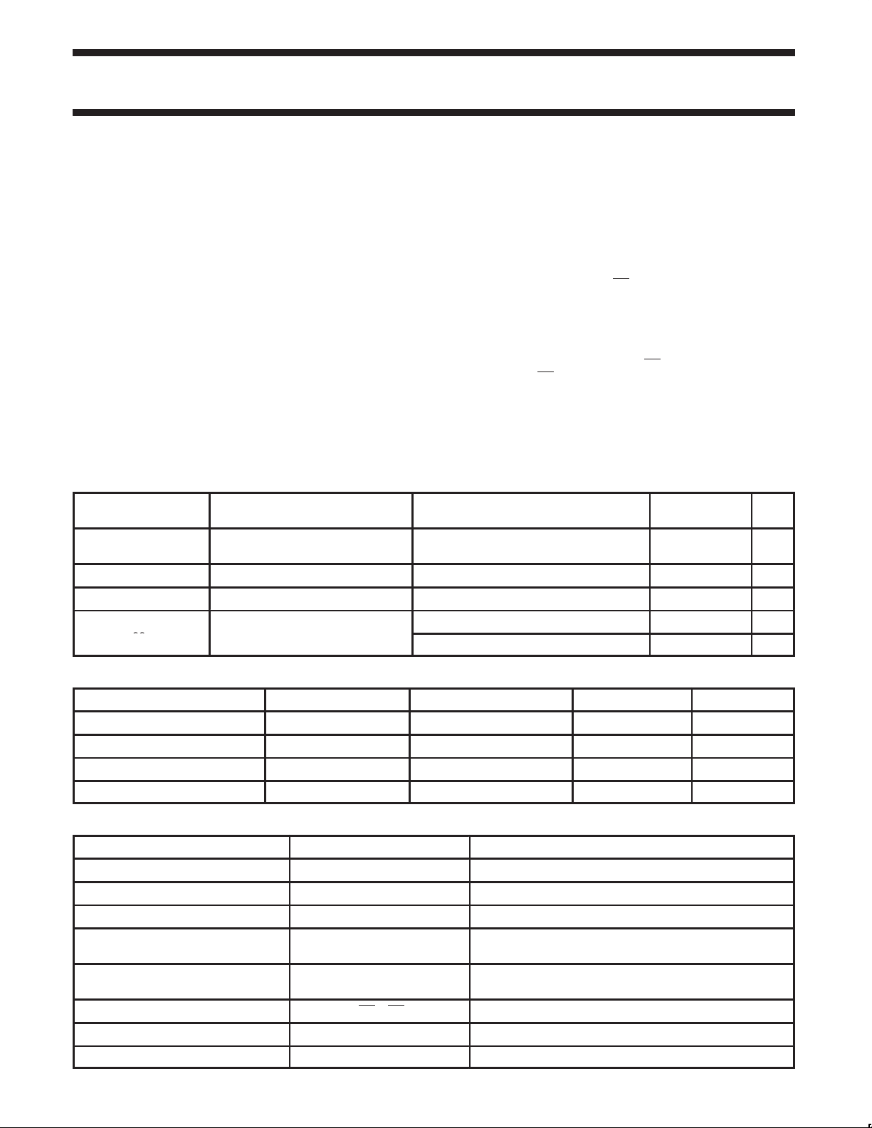
QUICK REFERENCE DATA

DESCRIPTION

The 74ABT16646 high±performance BiCMOS device combines low static and dynamic power dissipation with high speed and high output drive.

The 74ABT16646 16-bit transceiver/register consists of two sets of bus transceiver circuits with 3-State outputs, D-type flip-flops, and control circuitry arranged for multiplexed transmission of data directly from the input bus or from the internal registers. Data on the

A or B bus will be clocked into the registers as the appropriate clock pin goes High. Output Enable (nOE) and Direction (nDIR) pins are provided to control the transceiver function. In the transceiver mode, data present at the high impedance port may be stored in either the A or B register or both.

The select (nSAB, nSBA) pins determine whether data is stored or transferred through the device in real-time. The nDIR determines which bus will receive data when the nOE is active Low. In the isolation mode (nOE = High), data from Bus A may be stored in the B register and/or data from Bus B may be stored in the A register.

When an output function is disabled, the input function is still enabled and may be used to store and transmit data. Only one of the two buses, A or B may be driven at a time.

Two options are available, 74ABT16646 which does not have the bus-hold feature and 74ABTH16646 which incorporates the bus-hold feature.

SYMBOL

PARAMETER

CONDITIONS

TYPICAL

UNIT

Tamb = 25°C; GND = 0V


tPLH

Propagation delay

CL = 50pF; VCC = 5V

3.3

ns

tPHL

nAx to nBx

2.7


CIN

Input capacitance

VI = 0V or VCC

3

pF

CI/O

I/O capacitance

VO = 0V or VCC; 3-State

7

pF

ICCZ

Quiescent supply current

Outputs disabled; VCC =5.5V

550

μA

Outputs low; VCC =5.5V

9

mA


ORDERING INFORMATION

PACKAGES

TEMPERATURE RANGE

OUTSIDE NORTH AMERICA

NORTH AMERICA

DWG NUMBER


56-Pin Plastic SSOP Type III

±40°C to +85°C

74ABT16646 DL

BT16646 DL

SOT371-1


56-Pin Plastic TSSOP Type II

±40°C to +85°C

74ABT16646 DGG

BT16646 DGG

SOT364-1


56-Pin Plastic SSOP Type III

±40°C to +85°C

74ABTH16646 DL

BH16646 DL

SOT371-1


56-Pin Plastic TSSOP Type II

±40°C to +85°C

74ABTH16646 DGG

BH16646 DGG

SOT364-1


PIN DESCRIPTION

PIN NUMBER

SYMBOL

NAME AND FUNCTION


2, 55, 27, 30

1CPAB, 1CPBA, 2CPAB, 2CPBA

Clock input A to B / Clock input B to A


3, 54, 26, 31

1SAB, 1SBA, 2SAB, 2SBA

Select input A to B / Select input B to A


1, 28

1DIR, 2DIR

Direction control inputs


5, 6, 8, 9, 10, 12, 13, 14

1A0 ± 1A7,

Data inputs/outputs (A side)

15, 16, 17, 19, 20, 21, 23, 24

2A0 ± 2A7


52, 51, 49, 48, 47, 45, 44, 43

1B0 ± 1B7,

Data inputs/outputs (B side)

42, 41, 40, 38, 37, 36, 34, 33

2B0 ± 2B7


56, 29


Output enable inputs

1OE,

2OE


4, 11, 18, 25, 32, 39, 46, 53


GND

Ground (0V)


7, 22, 35, 50


VCC

Positive supply voltage

1998 Feb 27

2

853-1782 19026

Philips Semiconductors Product specification


16-bit bus transceiver/register (3-State)


74ABT16646


74ABTH16646


PIN CONFIGURATION


1DIR

1


56


1OE


1CPAB


1CPBA


2


55


1SAB


1SBA


3


54


GND


GND


4


53


1A0


1B0


5


52


1A1


1B1


6


51


VCC


7


50


VCC


1A2


8


49


1B2


1A3


1B3


9


48


1A4


1B4


10


47


GND


GND


11


46


1A5


1B5


12


45


1A6


1B6


13


44


1A7


1B7


14


43


2A0


2B0


15


42


2A1

16


41


2B1


2A2


2B2


17


40


GND


GND


18


39


2A3


2B3


19


38


2A4


2B4


20


37


2A5

21


36


2B5


VCC


22


35


VCC


2A6

23


34


2B6


2A7


24


33


2B7


GND


GND


25


32


2SAB


2SBA


26


31


2CPAB

27


30


2CPBA


2DIR


28


29


20E


SH00026


FUNCTION TABLE


INPUTS


DATA I/O

OPERATING MODE


nOE


nDIR


nCPAB

nCPBA

nSAB

nSBA


nAx

nBx


X


X


X


X

X


Input

Unspecified

Store A, B unspecified


output*


X


X


X


X

X

Unspecified

Input

Store B, A unspecified


output*


H


X


X

X


Input

Input

Store A and B data


H


X


H or L

H or L


X

X


Isolation, hold storage


L


L


X


X


X

L


Output

Input

Real time B data to A bus


L


L


X

H or L


X

H


Stored B data to A bus


L


H


X


X


L

X


Input

Output

Real time A data to B bus


L


H


H or L


X


H

X


Stored A data to B bus


H

=


High voltage level


L

=


Low voltage level


X

=


Don't care


=


Low-to-High clock transition


*The data output function may be enabled or disabled by various signals at the nOE input. Data input functions are always enabled, i.e., data at the bus pins will be stored on every Low±to±High transition of the clock.

1998 Feb 27

3

Philips 74ABTH16646DL, 74ABTH16646DGG, 74ABT16646DGG, 74ABT16646DL Datasheet

Philips Semiconductors

Product specification


16-bit bus transceiver/register (3-State)

74ABT16646

74ABTH16646


LOGIC SYMBOL (IEEE/IEC)

1OE

1DIR

1CPBA

1SBA

1CPAB

1SAB

2OE

2DIR

2CPBA

2SBA

2CPAB

2SAB

1A0

1A1

1A2

1A3

1A4

1A5

1A6

1A7

2A0

2A1

2A2

2A3

2A4

2A5

2A6

2A7

56

1

55

54

2

3

29

28

30

31

27

26

5

6

8

9

10

12

13

14

15

16

17

19

20

21

23

24

G3

3 EN1 [BA]

3 EN2 [AB]

C4

G5

C6

G7

G10

10 EN8 [BA]

10 EN9 [AB]

C11

G12

C13

G14


1

5


4D


1


5


1


6D

7


1


1


2


7


1


12


11D


8


12

1


13D

14


1


9


1


14


52

1B0

51

1B1

49

1B2

48

1B3

47

1B4

45

1B5

44

1B6

43

1B7

42

2B0

41

2B1

40

2B2

38

2B3

37

2B4

36

2B5

34

2B6

33

2B7

LOGIC SYMBOL

5

6

8

9

10

12

13

14

1A0 1A1 1A2 1A3 1A4 1A5 1A6 1A7

21CPAB

31SAB

1

1DIR


55

1CPBA


54

1SBA


56

1OE


1B0 1B1 1B2 1B3 1B4 1B5 1B6 1B7


52

51

49

48

47

45

44

43


15

16

17

19

20

21

23

24


2A0 2A1 2A2 2A3 2A4 2A5 2A6 2A7

27

2CPAB


26

2SAB


28

2DIR


302CPBA

312SBA

29 2OE

2B0 2B1 2B2 2B3 2B4 2B5 2B6 2B7

42 41 40 38 37 36 34 33

SH00027

SH00025

1998 Feb 27

4

Loading...
+ 8 hidden pages