

Philips 74ABTH16501ADGG, 74ABTH16501ADL, 74ABT16501ADL, 74ABT16501ADGG Datasheet

74ABT16501A
74ABTH16501A
18-bit universal bus transceiver (3-State)
Product specification
Supersedes data of 1997 Jun 12
IC23 Data Handbook
1998 Feb 27
INTEGRATED CIRCUITS
Philips Semiconductors Product specification
74ABT16501A
74ABTH16501A
18-bit universal bus transceiver (3-State)
2
1998 Feb 27 853-1788 19027
FEA TURES
•18-bit bidirectional bus interface
•3-State buffers
•Output capability: +64mA/-32mA
•TTL input and output switching levels
•74ABTH16501A incorporates bus-hold data inputs which
eliminate the need for external pull-up resistors to hold unused
inputs
•Live insertion/extraction permitted
•Power-up reset
•Power-up 3-State
•Positive edge-triggered clock inputs
•Latch-up protection exceeds 500mA per JEDEC Std 17
•ESD protection exceeds 2000V per MIL STD 883 Method 3015
and 200V per Machine Model
•Flexible operation permits 18 embedded D-type latches or
flip-flops to operate in clocked, transparent, and latched modes.
DESCRIPTION
The 74ABT16501A high-performance BiCMOS device combines low
static and dynamic power dissipation with high speed and high
output drive.
This device is an 18-bit universal transceiver featuring non-inverting
3-State bus compatible outputs in both send and receive directions.
Data flow in each direction is controlled by output enable (OEAB and
OEBA
), latch enable (LEAB and LEBA), and clock (CPAB and
CPBA) inputs. For A-to-B data flow, the device operates in the
transparent mode when LEAB is High. When LEAB is Low, the A
data is latched if CPAB is held at a High or Low logic level. If LEAB
is Low, the A-bus data is stored in the latch/flip-flop on the
Low-to-High transition of CP AB. When OEAB is High, the outputs
are active. When OEAB is Low, the outputs are in the
high-impedance state.
Data flow for B-to-A is similar to that of A-to-B but uses OEBA
,
LEBA and CPBA. The output enables are complimentary (OEAB is
active High, and OEBA
is active Low).
Active bus-hold circuitry is provided to hold unused or floating data
inputs at a valid logic level.
Two options are available, 74ABT16501A which does not have the
bus-hold feature and 74ABTH16501A which incorporates the
bus-hold feature.
QUICK REFERENCE DA TA
SYMBOL PARAMETER
CONDITIONS
T
amb
= 25°C; GND = 0V
TYPICAL UNIT
t
PLH
t
PHL
Propagation delay
An to Bn or Bn to An
CL = 50pF;
VCC = 5V
2.2
1.8
ns
C
IN
Input capacitance (Control pins) VI = 0V or V
CC
3 pF
C
I/O
I/O pin capacitance Outputs disabled; V
I/O
= 0V or V
CC
7 pF
I
CCZ
pp
Outputs disabled; VCC = 5.5V 500 µA
I
CCL
Quiescent supply current
Outputs low; VCC = 5.5V 9 mA
ORDERING INFORMATION
PACKAGES TEMPERATURE RANGE OUTSIDE NORTH AMERICA NORTH AMERICA DWG NUMBER
56-Pin Plastic SSOP Type III –40°C to +85°C 74ABT16501A DL BT16501A DL SOT371-1
56-Pin Plastic TSSOP Type II –40°C to +85°C 74ABT16501A DGG BT16501A DGG SOT364-1
56-Pin Plastic SSOP Type III –40°C to +85°C 74ABTH16501A DL BH16501A DL SOT371-1
56-Pin Plastic TSSOP Type II –40°C to +85°C 74ABTH16501A DGG BH16501A DGG SOT364-1
Philips Semiconductors Product specification
74ABT16501A
74ABTH16501A
18-bit universal bus transceiver (3-State)
1998 Feb 27
3
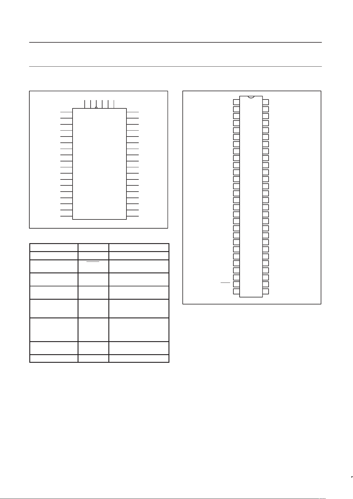
LOGIC SYMBOL
3
5
6
8
9
10
12
13
14
15
16
17
19
20
21
23
24
26
A0
A1
A2
A3
A5
A6
A7
A8
A9
A10
A11
A12
A13
A14
A15
A16
A17
A4
B0
B1
B2
B3
B4
B5
B6
B7
B8
B9
B10
B11
B12
B13
B14
B15
B16
B17
54
52
51
49
47
45
44
43
42
41
40
38
37
36
34
33
31
48
1255272830
CPBA
LEBA
OEBA
CPAB
LEAB
OEAB
SA00127
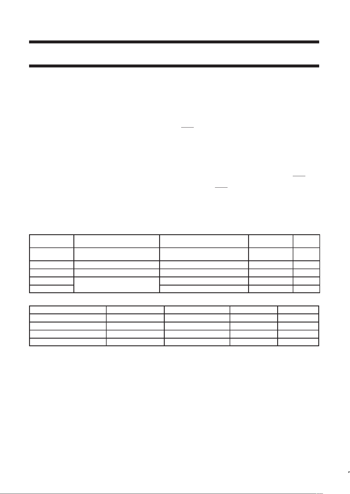
PIN DESCRIPTION
PIN NUMBER SYMBOL NAME AND FUNCTION
1 OEAB A-to-B Output enable input
27 OEBA B-to-A Output enable input
(active low)
2, 28 LEAB/LEBA A-to-B/B-to-A Latch
enable input
55,30 CPAB/
CPBA
A-to-B/B-to-A Clock input
(active rising edge)
3, 5, 6, 8, 9, 10, 12,
13, 14, 15, 16, 17,
19, 20, 21, 23, 24, 26
A0-A17
Data inputs/outputs
(A side)
54, 52, 51, 49, 48,
47, 45, 44, 43, 42,
41, 40, 38, 37, 36,
34, 33, 31
B0-B17
Data inputs/outputs
(B side)
4, 11, 18, 25, 32, 39,
46, 53
GND Ground (0V)
7, 22, 35, 50 V
CC
Positive supply voltage
PIN CONFIGURA TION
GND
GND
GND
GND
LEAB
OEAB
GND
V
CC
V
CC
GND GND
V
CC
V
CC
GND
GND
GND
LEBA
OEBA
1
2
3
4
5
6
7
8
9
10
11
12
13
14
15
16
17
18
19
20
21
22
23
24
25
26
27
28 29
30
31
32
33
34
35
36
37
38
39
40
41
42
43
44
45
46
47
48
49
50
51
52
53
54
55
56
A0
A1
A2
A3
A4
A5
A6
A7
A8
A9
A10
A11
A12
A13
A14
A15
A16
A17
CPAB
B0
B2
B1
B3
B4
B5
B6
B7
B8
B9
B10
B11
B12
B13
B14
B15
B16
B17
CPBA
SA00128
Philips Semiconductors Product specification
74ABT16501A
74ABTH16501A
18-bit universal bus transceiver (3-State)
1998 Feb 27
4
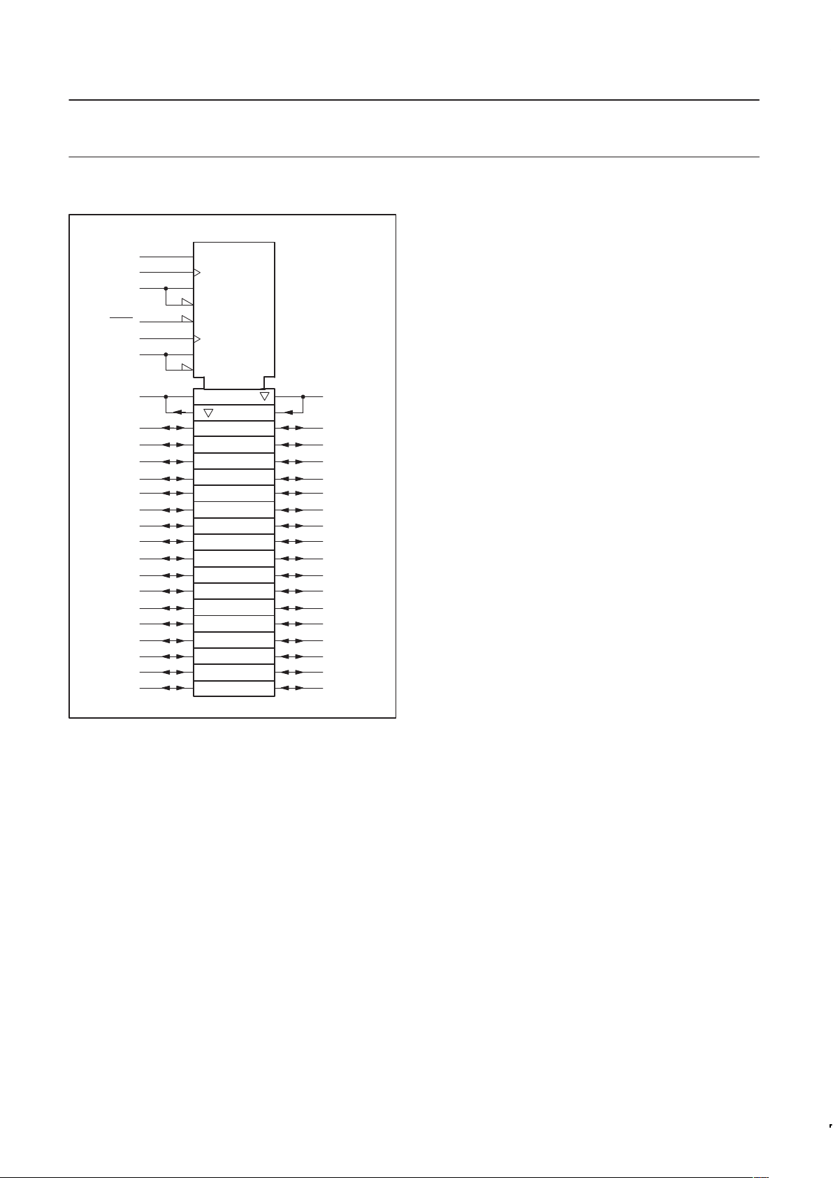
LOGIC SYMBOL (IEEE/IEC)
EN1
2C3
C3
G2
EN4
5C6
C6
G5
3D 1 1
416D
1
55
2
27
30
28
3
5
6
8
9
10
12
13
14
15
16
17
19
20
21
23
24
26
54
52
51
49
48
47
45
44
43
42
41
40
38
37
36
34
33
31
SA00129
OEAB
CPAB
LEAB
OEBA
CPBA
LEBA
A0
A1
A2
A3
A4
A5
A6
A7
A8
A9
A10
A11
A12
A13
A14
A15
A16
A17
B0
B1
B2
B3
B4
B5
B6
B7
B8
B9
B10
B11
B12
B13
B14
B15
B16
B17
 Loading...