

Philips 74ABTH16374BDL, 74ABTH16374BDGG, 74ABT16374BDL, 74ABT16374BDGG Datasheet
INTEGRATED CIRCUITS
74ABT16374B
74ABTH16374B
16-bit D-type flip-flop;
positive-edge trigger (3-State)
Product specification
Supersedes data of 1995 Sep 28
IC23 Data Handbook
1998 Feb 27
Philips Semiconductors Product specification
Quiescent su ly current
16-bit D-type flip-flop; positive-edge trigger
(3-State)
FEA TURES
•Two 8-bit positive edge triggered registers
•Live insertion/extraction permitted
•Power-up 3-State
•Power-up reset
•Multiple V
and GND pins minimize switching noise
CC
•3-State output buffers
•74ABTH16373B incorporates bus-hold data inputs which
eliminate the need for external pull-up resistors to hold unused
inputs
•Bus-hold data inputs eliminate the need for external pull-up
resistors to hold unused inputs
•Output capability: +64mA/–32mA
•Latch-up protection exceeds 500mA per JEDEC Std 17
•ESD protection exceeds 2000V per MIL STD 883 Method 3015
and 200V per Machine Model
DESCRIPTION
The 74ABT16374B high-performance BiCMOS device combines
low static and dynamic power dissipation with high speed and high
output drive.
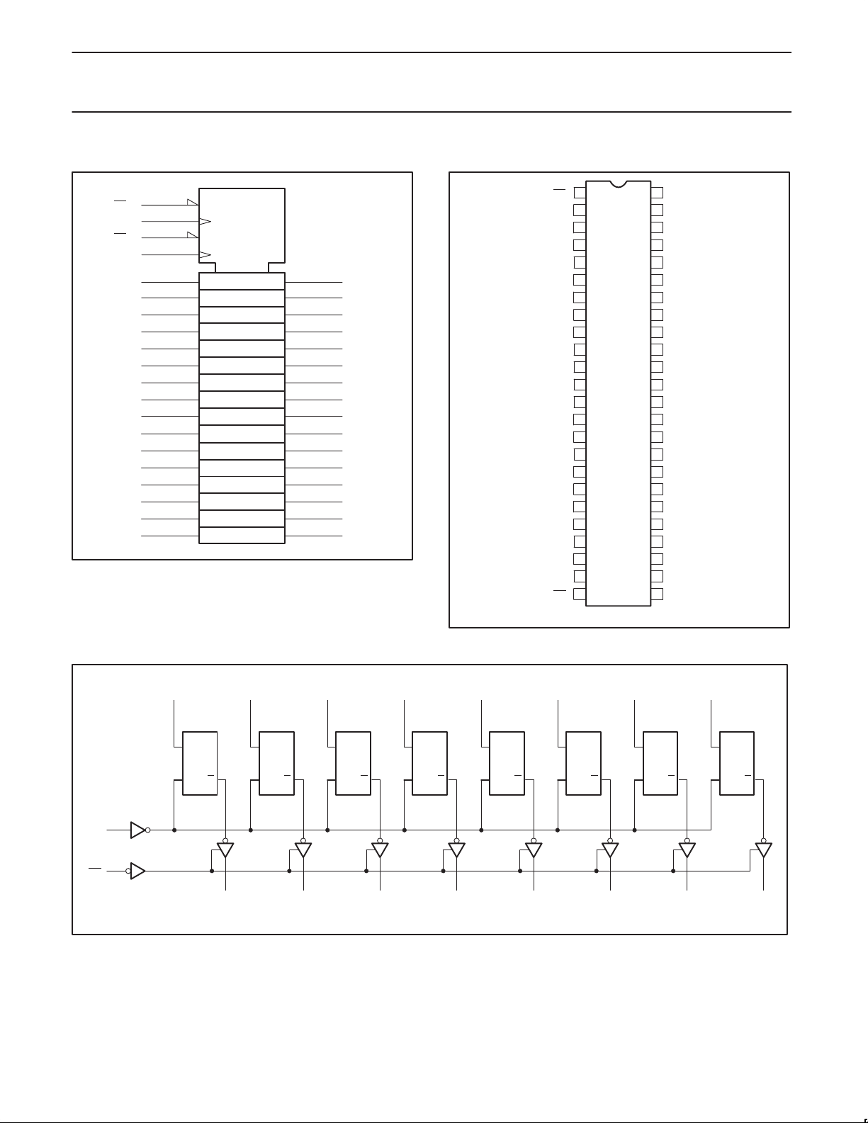
The 74ABT16374B has two 8-bit, edge triggered registers, with each
register coupled to eight 3-State output buffers. The two sections of
each register are controlled independently by the clock (nCP) and
Output Enable (nOE
Each register is fully edge triggered. The state of each D input, one
set-up time before the Low-to-High clock transition, is transferred to
the corresponding flip-flop’s Q output.
The 3-State output buffers are designed to drive heavily loaded
3-State buses, MOS memories, or MOS microprocessors. Each
active-Low Output Enable (nOE
its register independent of the clock operation.
When nOE
register. When nOE is High, the outputs for that register are in the
High-impedance “OFF” state, which means they will neither drive
nor load the bus.
Two options are available, 74ABT16374B which does not have the
bus-hold feature and 74ABTH16374B which incorporates the
bus-hold feature.
) control gates.
is Low, the stored data appears at the outputs for that
74ABT16374B
74ABTH16374B
) controls all eight 3-State buffers for
QUICK REFERENCE DATA
SYMBOL PARAMETER
C
t
PLH
t
PHL
C
OUT
I
CCZ
I
CCL
Propagation delay
nCP to nQx
Input capacitance VI = 0V or V
IN
Output capacitance VO = 0V or VCC; 3-State 7 pF
pp
CL = 50pF; VCC = 5V
Outputs disabled; VCC = 5.5V 500 µA
Outputs Low; VCC = 5.5V 8 mA
CONDITIONS
T
= 25°C; GND = 0V
amb
CC
TYPICAL UNIT
2.6
2.2
4 pF
ORDERING INFORMATION
PACKAGES TEMPERATURE RANGE OUTSIDE NORTH AMERICA NORTH AMERICA DWG NUMBER
48-Pin Plastic SSOP Type III –40°C to +85°C 74ABT16374B DL BT16374B DL SOT370-1
48-Pin Plastic TSSOP Type II –40°C to +85°C 74ABT16374B DGG BT16374B DGG SOT362-1
48-Pin Plastic SSOP Type III –40°C to +85°C 74ABTH16374B DL BH16374B DL SOT370-1
48-Pin Plastic TSSOP Type II –40°C to +85°C 74ABTH16374B DGG BH16374B DGG SOT362-1
ns
PIN DESCRIPTION
PIN NUMBER SYMBOL FUNCTION
47, 46, 44, 43, 41, 40, 38, 37
36, 35, 33, 32, 30, 29, 27, 26
2, 3, 5, 6, 8, 9, 11, 12
13, 14, 16, 17, 19, 20, 22, 23
4, 10, 15, 21, 28, 34, 39, 45 GND Ground (0V)
1998 Feb 27 853-1752 19027
1D0 – 1D7
2D0 – 2D7
1Q0 – 1Q7
2Q0 – 2Q7
1, 24 1OE, 2OE
48, 25 1CP, 2CP
7, 18, 31, 42 V
CC
Data inputs
Data outputs
Output enable
inputs (active-Low)
Clock pulse inputs
(active rising edge)
Positive supply
voltage
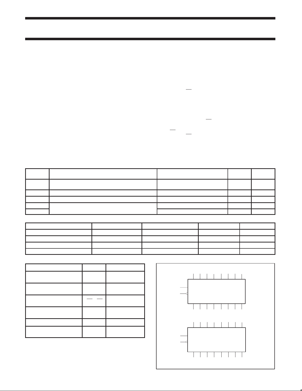
LOGIC SYMBOL
48
25
24
2
1
47 46 44 43
1D0 1D1 1D2 1D3
1CP
1OE
1Q0 1Q1 1Q2651Q3
32
36 35 33 32
2D02D21 2D2 2D3
2CP
2OE
2Q0 2Q1 2Q2 2Q3
1413 1716
41 40 38 37
1D4 1D5 1D6 1D7
1Q4 1Q5 1Q6
30 29 27 26
2D4 2D5 2D6 2D7
2Q4 2Q5 2Q6 2Q7
98
2019 2322
SH00078
1Q7
1211
Philips Semiconductors Product specification
16-bit D-type flip-flop; positive-edge trigger
(3-State)
LOGIC SYMBOL (IEEE/IEC)
1OE
1CP
2OE
2CP
1D0
1D1
1D2
1D3
1D4
1D5
1D6
1D7
2D0
2D1
2D2
2D3
2D4
2D5
2D6
2D7
1
48
24
25
47
46
44
43
41
40
38
37
36
35
33
32
30
29
27
1EN
2EN
1D
2D
C1
C2
1 ∇
2 ∇
2
3
5
6
8
9
11
12
13
14
16
17
19
20
22
2326
SH00077
1Q0
1Q1
1Q2
1Q3
1Q4
1Q5
1Q6
1Q7
2Q0
2Q1
2Q2
2Q3
2Q4
2Q5
2Q6
2Q7
PIN CONFIGURATION
1
1OE
2
1Q0
1Q1
3
GND
4
1Q2
5
6
1Q3
7
V
CC
8
1Q4
1Q5
9
GND
10
1Q6
11
1Q7
12
2Q0
13
2Q1
14
GND
15
16
2Q2
2Q3
17
18
V
CC
2Q4
19
20
2Q5
21
GND
22
2Q6
23
2Q7
24
2OE
74ABT16374B
74ABTH16374B
48
1CP
47
1D0
1D1
46
GND
45
1D2
44
43
1D3
42
V
CC
41
1D4
1D5
40
GND
39
1D6
38
1D7
37
2D0
36
2D1
35
GND
34
33
2D2
2D3
32
31
V
CC
2D4
30
29
2D5
28
GND
27
2D6
26
2D7
25
2CP
SA00326
LOGIC DIAGRAM
nD0
nCP
nOE
D
CP Q
nQ0
nD1
nD2
D
CP Q
nQ1 nQ2 nQ3 nQ4 nQ5 nQ6 nQ7
D
CP Q
nD3
D
CP Q
nD4
D
CP Q
nD5
D
CP Q
nD6
D
CP Q
nD7
D
CP Q
SA00327
1998 Feb 27
3
 Loading...