

Philips 74abt h16273 DATASHEETS
INTEGRATED CIRCUITS
74ABT16273
74ABTH16273
16-bit D-type flip-flop
Product specification
Supersedes data of 1995 Sep 28
IC23 Data Handbook
1998 Feb 27
Philips Semiconductors Product specification
Quiescent su ly current
16-bit D-type flip-flop
FEA TURES
•16-bit D-type edge triggered flip-flops
•Output capability: +64mA/–32mA
•TTL input and output switching levels
•Live insertion/extraction permitted
•Power-up reset
•74ABTH16273 incorporates bus-hold data inputs which eliminate
the need for external pull-up resistors to hold unused inputs
•Latch-up protection exceeds 500mA per JEDEC Std 17
•ESD protection exceeds 2000V per MIL STD 883 Method 3015
and 200V per Machine Model
QUICK REFERENCE DATA
SYMBOL PARAMETER
t
PLH
t
PHL
C
I
CCH
I
CCL
IN
Propagation delay
An to Bn or Bn to An
Input capacitance VI = 0V or V
pp
74ABT16273
74ABTH16273
DESCRIPTION
The 74ABT16273 high-performance BiCMOS device combines low
static and dynamic power dissipation with high speed and high
output drive.
This part is a 16-bit edge triggered D-type flip-flop with non-inverting
high drive outputs. This device can be used as two 8-bit flip-flops or
one 16-bit flip-flop. When the clock (CP) goes High, the data on the
D inputs is stored and the Q outputs display the stored data.
This device also features a master reset (MR
flip-flops to the Low state when MR
is set to the Low state.
Two options are available, 74ABT16273 which does not have the
bus-hold feature and 74ABTH16273 which incorporates the
bus-hold feature.
CONDITIONS
T
= 25°C; GND = 0V
amb
CL = 50pF;
VCC = 5.0V
CC
Outputs High; VCC = 5.5V 200 µA
Outputs low; VCC = 5.5V 8 mA
) that resets all
TYPICAL UNIT
2.5
2.0
ns
4 pF
ORDERING INFORMATION
PACKAGES TEMPERATURE RANGE OUTSIDE NORTH AMERICA NORTH AMERICA DWG NUMBER
48-Pin Plastic SSOP Type III –40°C to +85°C 74ABT16273 DL BT16273 DL SOT370-1
48-Pin Plastic TSSOP Type II –40°C to +85°C 74ABT16273 DGG BT16273 DGG SOT362-1
48-Pin Plastic SSOP Type III –40°C to +85°C 74ABTH16273 DL BH16273 DL SOT370-1
48-Pin Plastic TSSOP Type II –40°C to +85°C 74ABTH16273 DGG BH16273 DGG SOT362-1
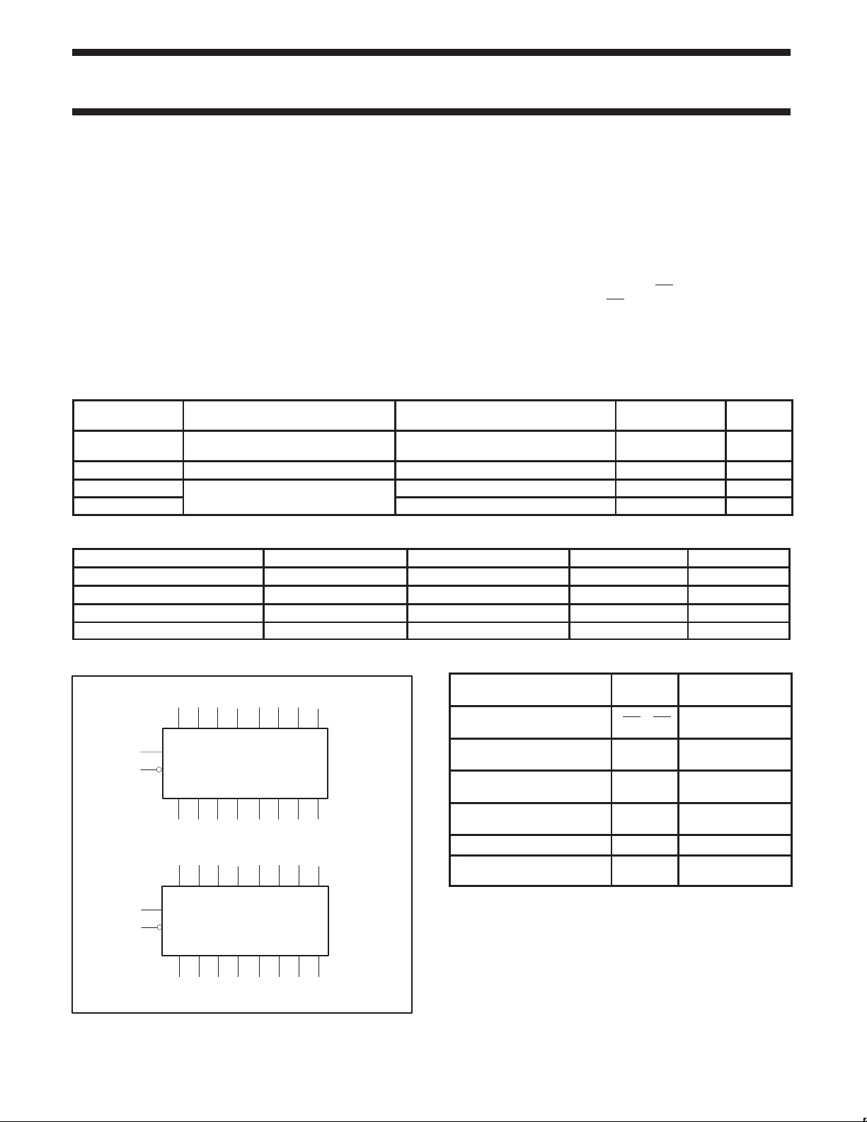
LOGIC SYMBOL
1
1D0 1D1 1D2 1D3
CP
MR
1Q0 1Q1 1Q2651Q3
CP
MR
2Q0 2Q1 2Q2 2Q3
48
25
24
47 46 44 43
32
36 35 33 32
2D02D21 2D2 2D3
41 40 38 37
1D4 1D5 1D6 1D7
1Q4 1Q5 1Q6
30 29 27 26
2D4 2D5 2D6 2D7
2Q4 2Q5 2Q6 2Q7
1Q7
98
1211
PIN DESCRIPTION
PIN NUMBER SYMBOL
1, 24 1MR, 2MR
2, 3, 5, 6, 8, 9, 11, 12,13,
14, 16, 17, 19, 20, 22, 23
47, 46, 44, 43, 41, 40, 38, 37,
36, 35, 33, 32, 30, 29, 27, 26
1Q0-1Q7
2Q0-2Q7
1D0-1D7
2D0-2D7
25, 48 1CP, 2CP
4, 10, 15, 21, 28, 34, 39, 45 GND Ground (0V)
7, 18, 31, 42 V
CC
NAME AND
FUNCTION
Master reset input
(active-Low)
Data outputs
Data inputs
Clock pulse input
(active rising edge)
Positive supply
voltage
1998 Feb 27 853-1793 19027
1413 1716
2019 2322
SH00052
2
Philips Semiconductors Product specification
16-bit D-type flip-flop
LOGIC SYMBOL (IEEE/IEC)
1
1MR
48
CP
24
2MR
25
2CP
47
1D0
46
1D1
44
1D2
43
1D3
41
1D4
40
1D5
38
1D6
37
1D7
36
2D0
35
2D1
33
2D2
32
2D3
30
2D4
29
2D5
27
2D6
26
2D7
FUNCTION TABLE
Inputs Output
nMR nCP nDX nQ0-nQ7
L X X L Reset (clear)
H ↑ h H Load “1”
H ↑ I L Load “0”
H L X Q
H = High voltage level
h = high voltage level one set-up time prior to the Low-to-High
clock transition
L = Low voltage level
I = Low voltage level one set-up time prior to the Low-to-High
clock transition
X = Don’t care
↑ = Low-to-High clock transition
0= Output as it was
Q
R1
C1
R2
C2
1 ∇1D
2D
2 ∇
2
3
5
6
8
9
11
12
13
14
16
17
19
20
22
23
SH00053
1Q0
!Q1
1Q2
1Q3
1Q4
1Q5
1Q6
1Q7
2Q0
2Q1
2Q2
2Q3
2Q4
2Q5
2Q6
2Q7
operating
mode
0
Retain state
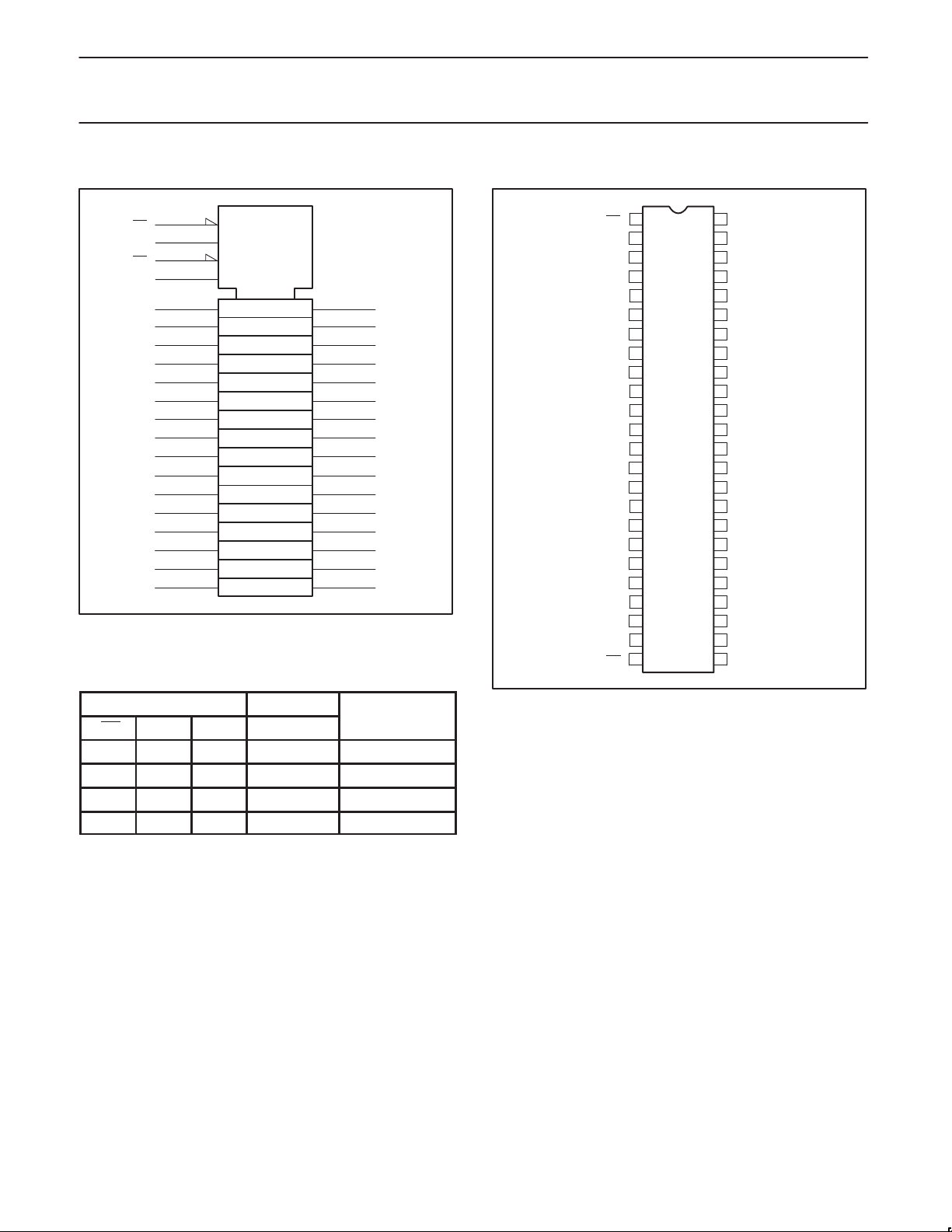
PIN CONFIGURATION
1
1MR
2
1Q0
!Q1
3
GND
4
1Q2
5
1Q3
6
7
V
CC
8
1Q4
1Q5
9
GND
10
1Q6
11
1Q7
12
2Q0
13
2Q1
14
GND
15
16
2Q2
2Q3
17
18
V
CC
2Q4
19
20
2Q5
21
GND
22
2Q6
23
2Q7
24
2MR
74ABT16273
74ABTH16273
48
CP
47
1D0
1D1
46
GND
45
1D2
44
1D3
43
42
V
CC
41
1D4
1D5
40
GND
39
1D6
38
1D7
37
2D0
36
2D1
35
GND
34
33
2D2
32
2D3
31
V
CC
2D4
30
29
2D5
28
GND
27
2D6
26
2D7
25
2CP
SH00054
1998 Feb 27
3
 Loading...