

Philips 74ABTH16260DL, 74ABTH16260DGG, 74ABT16260DL, 74ABT16260DGG Datasheet

INTEGRATED CIRCUITS
74ABT16260/74ABTH16260
12-bit to 24-bit multiplexed D-type latches
(3-State)
Product specification
Supersedes data of 1996 Nov 20
IC23 Data Handbook
1998 Feb 10
Philips Semiconductors Product specification
C
pF
ns
12-bit to 24-bit multiplexed D-type latches (3-State)
FEATURES
•ESD protection exceeds 2000V per Mil-Std-883C, Method 3015;
exceeds 200V using machine model (C = 200pF, R = 0).
•Latch-up performance exceeds 500mA per JEDEC Standard
JESD-17.
•Distributed V
switching noise.
and GND pin configuration minimizes high-speed
CC
•Flow-through architecture optimizes PCB layout.
•High-drive outputs (–32mA I
, 64mA IOL).
OH
•74ABTH16260 incorporates bus-hold inputs which eliminate the
need for external pull-up resistors.
•Package options:
– 56-pin plastic Shrink Small-Outline Package (SSOP)
– 56-pin plastic Thin Shrink Small-Outline Package (TSSOP)
DESCRIPTION
The 74ABT16260/74ABTH16260 is a 12-bit to 24-bit multiplexed
D-type latch used in applications where two separate data paths
must be multiplexed onto, or demultiplexed from, a single data path.
Typical applications include multiplexing and/or demultiplexing of
address and data information in microprocessor or bus-interface
applications. This device is alto useful in memory-interleaving
applications.
Three 12-bit I/O ports (A1–A12, 1B1–1B12, and 2B1–2B12) are
available for address and/or data transfer. The output enable (OE1B
, and OEA) inputs control the bus transceiver functions. The
OE2B
OE1B
and OE2B control signals also allow bank control in the A to
B direction.
Address and/or data information can be stored using the internal
storage latches. The latch enable (LE1B, LE2B, LEA1B, and
LEA2B) inputs are used to control data storage. When the latch
enable input is high, the latch is transparent. When the latch enable
input goes low, the data present at the inputs is latched and remains
latched until the latch enable input is returned high.
To ensure the high-impedance state during power-up or
power-down, OE
the minimum value of the resistor is determined by the current
sinking capability of the driver.
The 74ABTH incorporates the bus hold feature. The 74ABT does
not include bus hold feature. Both parts are available in 56-pin
SSOP and TSSOP.
74ABT16260
74ABTH16260
,
should be tied to VCC through a pull-up resistor;
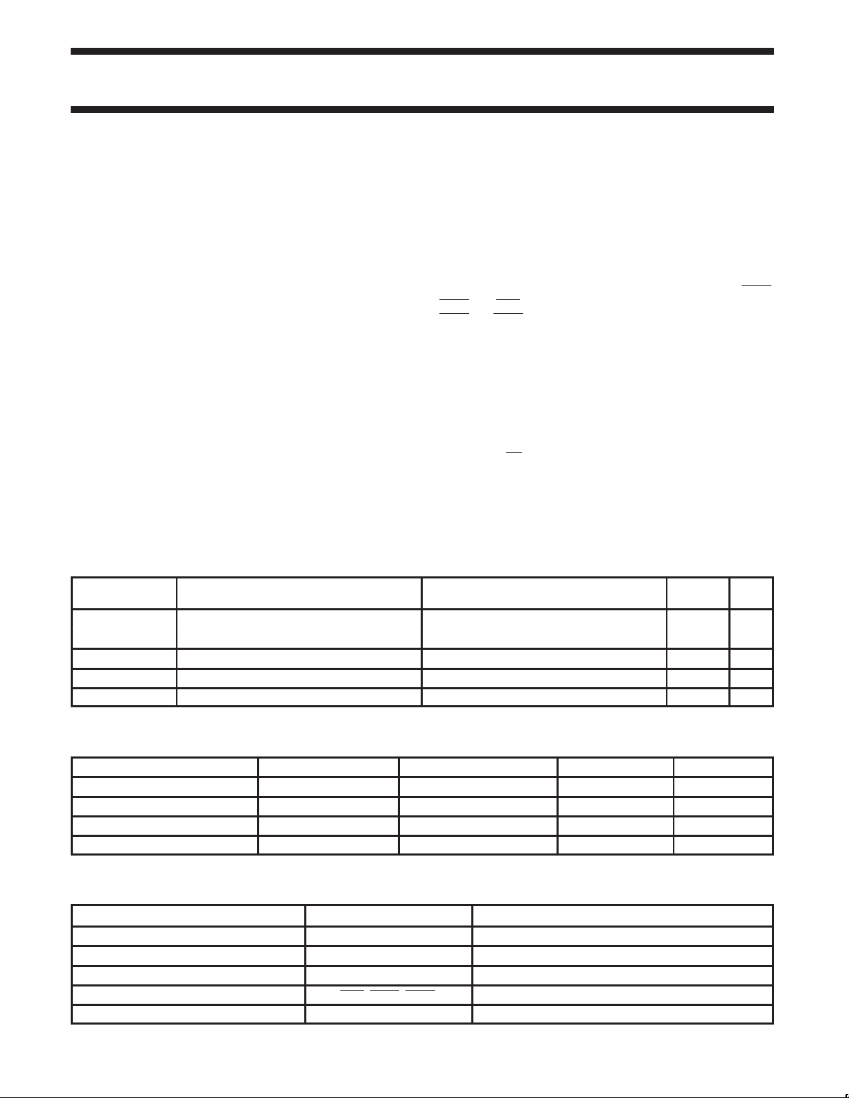
QUICK REFERENCE DATA
SYMBOL PARAMETER
C
t
PLH
t
PHL
C
OUT
I
CCZ
IN
Propagation delay
nAx to nBx nBx to nAx
Input capacitance VI = 0 V or V
Output capacitance V
Total supply current Outputs disabled 100 µA
CONDITIONS
T
= 25°C; GND = 0V
amb
p
= 50
L
CC
= 0 V or 5.0 V 6 pF
I/O
TYPICAL UNIT
2.8
2.5
4 pF
ORDERING INFORMATION
PACKAGES TEMPERATURE RANGE OUTSIDE NORTH AMERICA NORTH AMERICA DWG NUMBER
56-Pin Plastic SSOP Type III –40°C to +85°C 74ABT16260 DL BT16260 DL SOT371-1
56-Pin Plastic TSSOP Type II –40°C to +85°C 74ABT16260 DGG BT16260 DGG SOT364-1
56-Pin Plastic SSOP Type III –40°C to +85°C 74ABTH16260 DL BH16260 DL SOT371-1
56-Pin Plastic TSSOP Type II –40°C to +85°C 74ABTH16260 DGG BH16260 DGG SOT364-1
PIN DESCRIPTION
PIN NUMBER SYMBOL FUNCTION
8, 9, 10, 12, 13, 14, 15, 16, 17, 19, 20, 21 An Data inputs/outputs (A)
23, 24, 26, 31, 33, 34, 36, 37, 38, 40, 41, 42 1Bn Data inputs/outputs (B1)
6, 5, 3, 54, 52, 51, 49, 48, 47, 45, 44, 43 2Bn Data inputs/outputs (B2)
1, 29, 56 OEA, OE1B, OE2B Output enable input (active low)
2, 27, 30, 55 LE1B, LE2B, LEA1B, LEA2B Latch enable inputs
1998 Feb 10 853-2048-18945
2
Philips Semiconductors Product specification
12-bit to 24-bit multiplexed D-type latches (3-State)
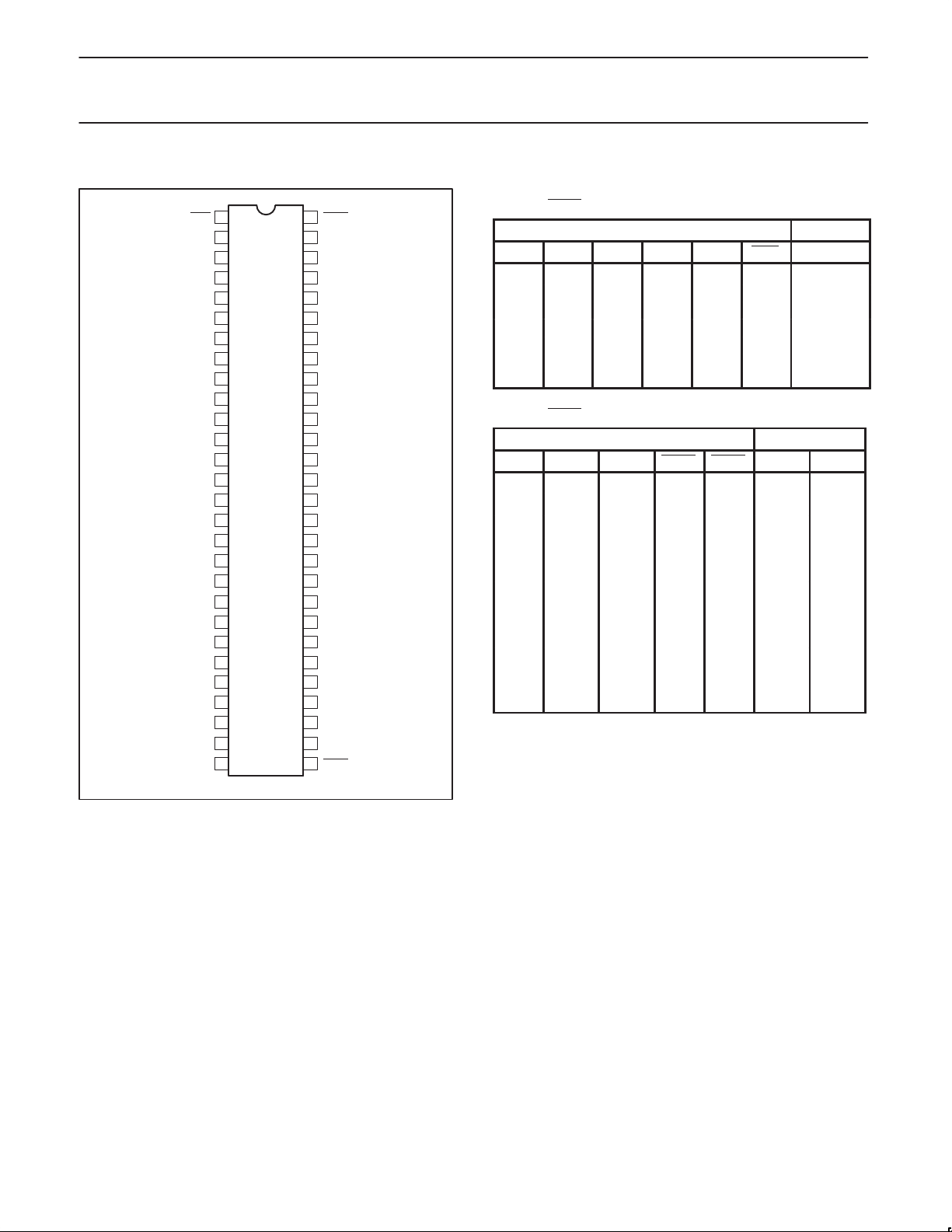
PIN CONFIGURATION
1
2
LE1B
2B3
3
GND
4
2B2
5
2B1
6
V
7
CC
A1
8
A2
9
A3
10
GND
11
12 45
13
A6
14
A7
15
A8
16
A9
17
GND
18 39
19 38
A10
20
21
A12
22
V
CC
23
1B1
24
1B2
25 32
26 31 1B41B3
27 30 LEA1BLE2B
28 29SEL OE1B
OE2B
56OEA
55
LEA2B
54
2B4
53
GND
52
2B5
51
2B6
50
V
CC
2B7
49
2B8
48
47
2B9
46
GND
2B10A4
2B11
44A5
2B12
43
1B12
42
1B11
41
1B10
40
GND
1B9
37A11
1B8
36
1B7
V
35
CC
34
1B6
33
1B5
GNDGND
FUNCTION TABLES
B to A (OEB = H)
1B 2B SEL LE1B LE2B OEA A
H X H H X L H
L X H H X L L
X X H L X L A0
X H L X H L H
X L L X H L L
X X L X L L A0
X X X X X H Z
A to B (OEA = H)
A LEA1B LEA2B OE1B OE2B 1B 2B
H H H L L H H
L H H L L L L
H H L L L H 2B0
L H L L L L 2B0
H L H L L 1B0 H
L L H L L 1B0 L
X L L L L 1B0 2B0
X X X H H Z Z
X X X L H Active Z
X X X H L Z Active
X X X L L Active Active
74ABT16260
74ABTH16260
INPUTS OUTPUT
INPUTS OUTPUT
1998 Feb 10
SA00435
3

Philips Semiconductors Product specification
12-bit to 24-bit multiplexed D-type latches (3-State)
LOGIC DIAGRAM (POSITIVE LOGIC)
2
LE1B
27
LE2B
30
LEA1B
55
LEA2B
56
OE2B
29
OE1B
1
OEA
28
SEL
G1
8
A1
1
1
74ABT16260
74ABTH16260
C1
1D
23
1B1
C1
1D
C1
1D
C1
1D
TO 11 OTHER CHANNELS
6
SA00436
2B1
1998 Feb 10
4
 Loading...