

Philips 74ABTH162240DL, 74ABTH162240DGG, 74ABT162240DL, 74ABT162240DGG Datasheet

INTEGRATED CIRCUITS
74ABT162240
74ABTH162240
16-bit inverting buffer/driver with 30
series termination resistors
Product specification
Supersedes data of 1998 Jan 16
IC23 Data Handbook
1998 Feb 25
Philips Semiconductors Product specification
Quiescent su ly current
16-bit inverting buffer/driver with 30Ω series
termination resistors (3-State)
FEA TURES
•16-bit bus interface
•3-State buffers
•Output capability: +12mA/-32mA
•TTL input and output switching levels
•Bus-hold data inputs eliminate the need for external pull-up
resistors to hold unused inputs
•Live insertion/extraction permitted
DESCRIPTION
The 74ABT162240 is a high-performance BiCMOS device which
combines low static and dynamic power dissipation with high speed.
This device is an inverting 16-bit buffer that is ideal for driving bus
lines. The device features four Output Enables (1OE
4OE
Two options are available, 74ABT162240 which does not have the
bus hold feature and 74ABTH162240 which incorporates the bus
hold feature.
), each controlling four of the 3-State outputs.
74ABT162240
74ABTH162240
, 2OE, 3OE,
•Power-up 3-State
•74ABTH162240 incorporates bus hold data inputs which eliminate
the need for external pull up resistors to hold unused inputs
•Latch-up protection exceeds 500mA per JEDEC Std 17
•ESD protection exceeds 2000V per MIL STD 883 Method 3015
and 200V per Machine Model
QUICK REFERENCE DATA
SYMBOL PARAMETER
C
t
PLH
t
PHL
C
OUT
I
CCZ
I
CCL
IN
Propagation delay
nAx to nYx
CL = 50pF;
VCC =
Input capacitance nOE VI = 0V or 3.0V 4 pF
Output capacitance Outputs disabled; VO = 0V or 6 pF
pp
Outputs disabled; VCC = 500 µA
Outputs low; VCC = 5.5V 8 mA
ORDERING INFORMATION
PACKAGES TEMPERATURE RANGE OUTSIDE NORTH AMERICA NORTH AMERICA DWG NUMBER
48-Pin Plastic SSOP Type III –40°C to +85°C 74ABT162240 DL BT162240 DL SOT370-1
48-Pin Plastic TSSOP Type II –40°C to +85°C 74ABT162240 DGG BT162240 DGG SOT362-1
48-Pin Plastic SSOP Type III –40°C to +85°C 74ABTH162240 DL BH162240 DL SOT370-1
48-Pin Plastic TSSOP Type II –40°C to +85°C 74ABTH162240 DGG BH162240 DGG SOT362-1
CONDITIONS
T
= 25°C
amb
TYPICAL UNIT
2.7
2.6
ns
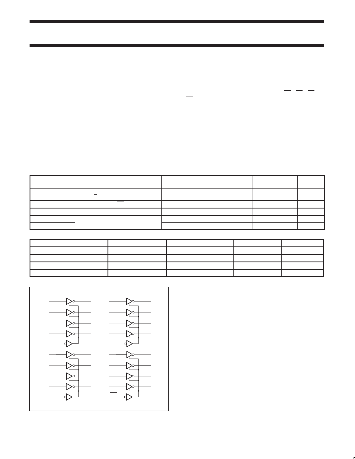
LOGIC SYMBOL
47
46
44
43
1
41
40
38
37
48
1998 Feb 25 853-1825 19019
1A0
1A1
1A2
1A3
1OE
2A0
2A1
2A2
2A3
2OE
1Y0
1Y1
1Y2
1Y3
2Y0
2Y1
2Y2
2Y3
3A0
36
2
3A1
35
3
3A2
33
5
3A3
32
6
3OE
25
4A0
8
30
4A1
9
29
4A2
11
27
4A3
26
12
4OE
24
3Y0
3Y1
3Y2
3Y3
4Y0
4Y1
4Y2
4Y3
SH00090
13
14
16
17
19
20
22
23
2
Philips Semiconductors Product specification
16-bit inverting buffer/driver with 30Ω series
termination resistors (3-State)
LOGIC SYMBOL (IEEE/IEC)
1OE
2OE
3OE
4OE
1A1
1A2
1A3
1A4
2A1
2A2
2A3
2A4
3A1
3A2
3A3
3A4
4A1
4A2
4A3
4A4
1
48
25
24
47
46
44
43
41
40
38
37
36
35
33
32
30
29
27
26
EN1
EN2
EN3
EN4
2
1 ∇
1
2 ∇1
3 ∇1
4 ∇1
1Y1
3
1Y2
5
1Y3
6
1Y4
8
2Y1
9
2Y2
11
2Y3
12
2Y4
13
3Y1
14
3Y2
16
3Y3
17
3Y4
19
4Y1
20
4Y2
22
4Y3
23
4Y4
SH00085
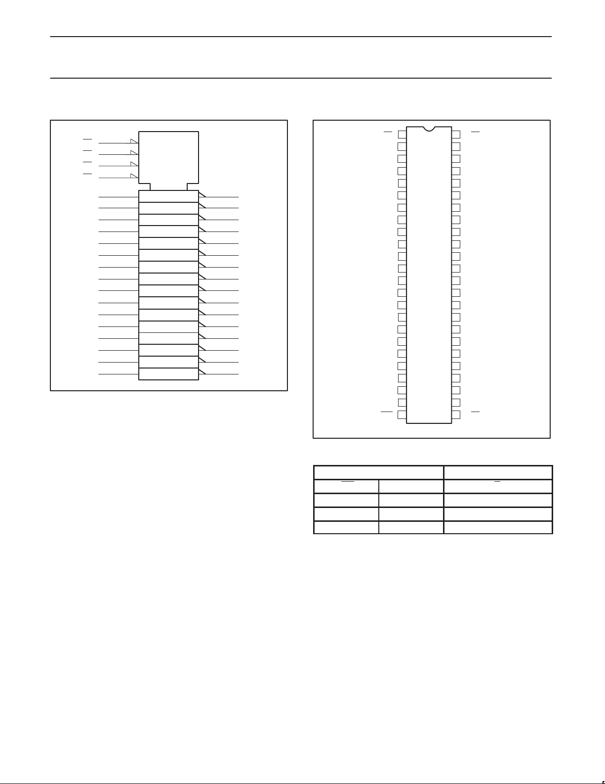
PIN CONFIGURA TION
1
1OE
2
1Y0
3
1Y1
4
GND
5
1Y2
6
1Y3
7
V
CC
8
2Y0
9
2Y1
10
GND
11
2Y2
12
2Y3
13
3Y0
14
3Y1
15
GND
16
3Y2
17
3Y4
18
V
CC
19
4Y0
20
4Y1
21
GND
22
4Y2
23
4Y3
24
4OE
74ABT162240
74ABTH162240
48
2OE
47
1A0
46
1A1
45
GND
44
1A2
43
1A3
42
V
CC
41
2A0
40
2A1
39
GND
38
2A2
37
2A3
36
3A0
35
3A1
34
GND
33
3A2
32
3A3
V
31
CC
30
4A0
29
4A1
28
GND
27
4A2
26
4A3
25
3OE
FUNCTION TABLE
Inputs Outputs
nOE nAx nYx
L L H
L H L
H X Z
H = High voltage level
L = Low voltage level
X = Don’t care
Z = High Impedance “off” state
SA00013
1998 Feb 25
3
Philips Semiconductors Product specification
16-bit inverting buffer/driver with 30Ω series
termination resistors (3-State)
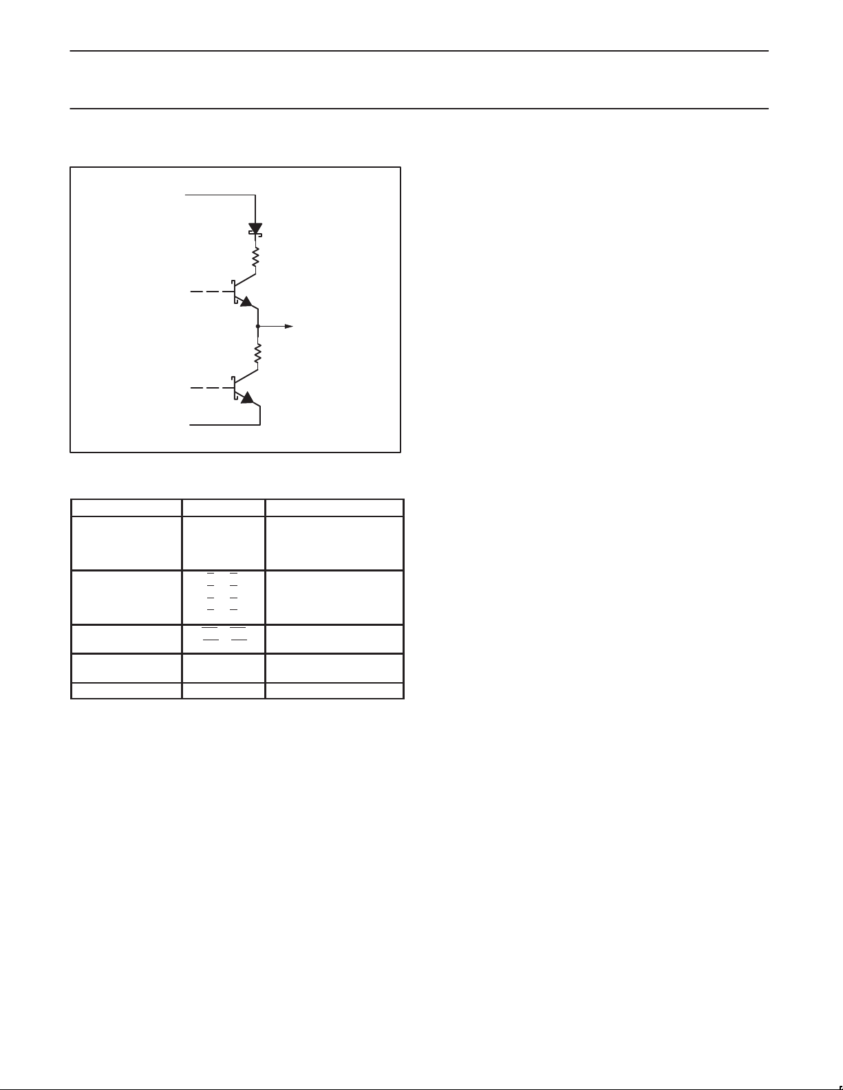
SCHEMATIC OF Y OUTPUTS
V
CC
27Ω
OUTPUT
27Ω
GND
SA00042
74ABT162240
74ABTH162240
PIN DESCRIPTION
PIN NUMBER SYMBOL NAME AND FUNCTION
47, 46, 44, 43,
41, 40, 38, 37,
36, 35, 33, 32,
30, 29, 27, 26
2, 3, 5, 6,
8, 9, 11, 12,
13, 14, 16, 17,
19, 20, 22, 23
1, 48, 25, 24
4, 10, 15, 21,
28, 34, 39, 45
7, 18, 31, 42 V
1A0-1A3
2A0-2A3
3A0-3A3
4A0-4A3
1Y0-1Y3
2Y0-2Y3
3Y0-3Y3
4Y0-4Y3
1OE, 2OE,
3OE, 4OE
GND Ground (0V)
CC
Data inputs
Data outputs
Output enables
Positive supply voltage
1998 Feb 25
4
 Loading...