

Philips 74ABT899DB, 74ABT899D, 74ABT899A Datasheet

INTEGRATED CIRCUITS
74ABT899
9-bit dual latch transceiver with 8-bit
parity generator/checker (3-State)
Product specification
Supersedes data of 1993 Oct 04
IC23 Data Handbook
1998 Jan 16

Philips Semiconductors Product specification
9-bit dual latch transceiver with 8-bit parity
generator/checker (3-State)
FEA TURES
•Symmetrical (A and B bus functions are identical)
•Selectable generate parity or ”feed-through” parity for A-to-B and
B-to-A directions
•Independent transparent latches for A-to-B and B-to-A directions
•Selectable ODD/EVEN parity
•Continuously checks parity of both A bus and B bus latches as
and ERRB
ERRA
•Ability to simultaneously generate and check parity
•Can simultaneously read/latch A and B bus data
•Output capability: +64 mA/–32mA
•Latch-up protection exceeds 500mA per Jedec JC40.2 Std 17
•ESD protection exceeds 2000 V per MIL STD 883 Method 3015
and 200 V per Machine Model
•Power up 3-State
•Power-up reset
•Live insertion/extraction permitted
DESCRIPTION
The 74ABT899 is a 9-bit to 9-bit parity transceiver with separate
transparent latches for the A bus and B bus. Either bus can
generate or check parity. The parity bit can be fed-through with no
change or the generated parity can be substituted with the SEL
input.
Parity error checking of the A and B bus latches is continuously
provided with ERRA
The 74ABT899 features independent latch enables for the A and B
bus latches, a select pin for ODD/EVEN
signal output pins for checking parity.
FUNCTIONAL DESCRIPTION
The 74ABT899 has three principal modes of operation which are
outlined below. All modes apply to both the A-to-B and B-to-A
directions.
Transparent latch, Generate parity, Check A and B bus parity:
Bus A (B) communicates to Bus B (A), parity is generated and
passed on to the B (A) Bus as BPAR (APAR). If LEA and LEB are
High and the Mode Select (SEL
A0-A7 and B0-B7 can be checked and monitored by ERRA
ERRB
74ABT899
and ERRB, even with both buses in 3-State.
parity, and separate error
) is Low, the parity generated from
and
. (Fault detection on both input and output buses.)
QUICK REFERENCE DATA
SYMBOL PARAMETER
t
PLH
t
PHL
t
PLH
t
PHL
C
C
I
CCZ
I/O
Propagation delay
An to Bn or Bn to An
Propagation delay
An to ERRA
Input capacitance VI = 0V or V
IN
Output capacitance Outputs disabled; VO = 0V or V
Total supply current Outputs disabled; VCC =5.5V 50 µA
Transparent latch, Feed-through parity, Check A and B bus
parity:
Bus A (B) communicates to Bus B (A) in a feed-through mode if SEL
is High. Parity is still generated and checked as ERRA and ERRB
and can be used as an interrupt to signal a data/parity bit error to the
CPU.
Latched input, Generate/Feed-through parity, Check A (and B)
bus parity:
Independent latch enables (LEA and LEB) allow other permutations of:
•Transparent latch / 1 bus latched / both buses latched
•Feed-through parity / generate parity
•Check in bus parity / check out bus parity / check in and out bus
parity
CONDITIONS
T
= 25°C; GND = 0V
amb
CL = 50pF; VCC = 5V 2.9 ns
CL = 50pF; VCC = 5V 6.1 ns
CC
CC
TYPICAL UNIT
4 pF
7 pF
ORDERING INFORMATION
PACKAGES TEMPERATURE RANGE OUTSIDE NORTH AMERICA NORTH AMERICA DWG NUMBER
28-Pin Plastic PLCC –40°C to +85°C 74ABT899 A 74ABT899 A SOT261-3
28-Pin Plasti c SOP –40°C to +85°C 74ABT899 D 74ABT899 D SOT136-1
28-Pin Plasti c SSOP –40°C to +85°C 74ABT899 DB 74ABT899 DB SOT341-1
1998 Jan 16 853-1623 18864
2
Philips Semiconductors Product specification
9-bit dual latch transceiver with 8-bit parity
generator/checker (3-State)
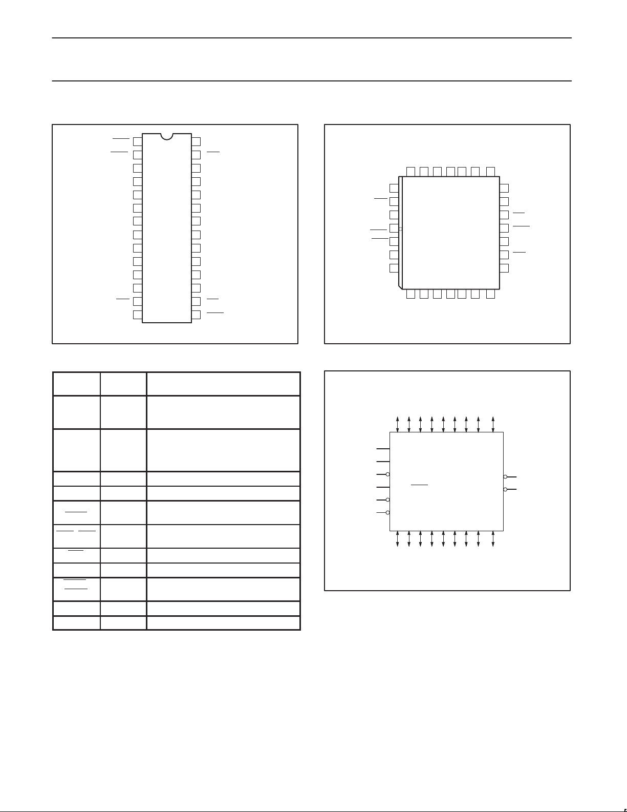
PIN CONFIGURATION
ODD/EVEN
1
227
ERRA OEB
3
LEA
4
A0
5
A1
6
A2
7
A3
APAR
TOP VIEW
8
A4
9
A5
10
A6
11
A7 BPAR
12 17
13 16OEA
14 15GND
28
V
B0
26
25
B1
24
B2
23
B3
22
B4
21
B5
20
B6
19
B7
18
LEB
SEL
ERRB
SA00289
CC
PLCC PIN CONFIGURATION
B1 B2 B3 B4 B5 B6 B7
25
24 23 22 21 20 19
B0
26
OEB
27
28
V
CC
ODD/
1
EVEN
2
ERRA
3
LEA
4
A0
67891011
5
A1 A2 A3 A4 A5 A6 A7
74ABT899
18
BPAR
17
LEB
16
SEL
15
ERRB
14 GND
13
OEA
12
APAR
SA00291
PIN DESCRIPTION
SYMBOL
A0 - A7
B0 - B7
APAR 12 A bus parity 3-State input
BPAR 18 B bus parity 3-State input
ODD/
EVEN
OEA, OEB 13, 27
SEL 16 Mode select input (Low for generate)
LEA, LEB 3, 17 Latch enable inputs (transparent High)
ERRA,
ERRB
GND 14 Ground (0V)
V
CC
PIN
NUMBER
NAME AND FUNCTION
4, 5, 6, 7,
8, 9, 10,
Latched A bus 3-State inputs/outputs
11
19, 20,
21, 22,
23, 24,
Latched B bus 3-State inputs/outputs
25, 26
Parity select input (Low for EVEN
1
parity)
Output enable inputs (gate A to B,
B to A)
2, 15 Error signal outputs (active-Low)
28 Positive supply voltage
LOGIC SYMBOL
A0 A1 A2 A3 A4 A5 A6 A7
3
17
16
1
27
13
B0 B1 B2 B3 B4 B5 B6 B7
26 25 24 23 22 21 20 19
4567 891011
LEA
LEB
SEL
ODD/EVEN
OEB
OEA
ERRA
ERRB
12
APAR
2
15
BPAR
18
SA00290
1998 Jan 16
3
Philips Semiconductors Product specification
9-bit dual latch transceiver with 8-bit parity
generator/checker (3-State)
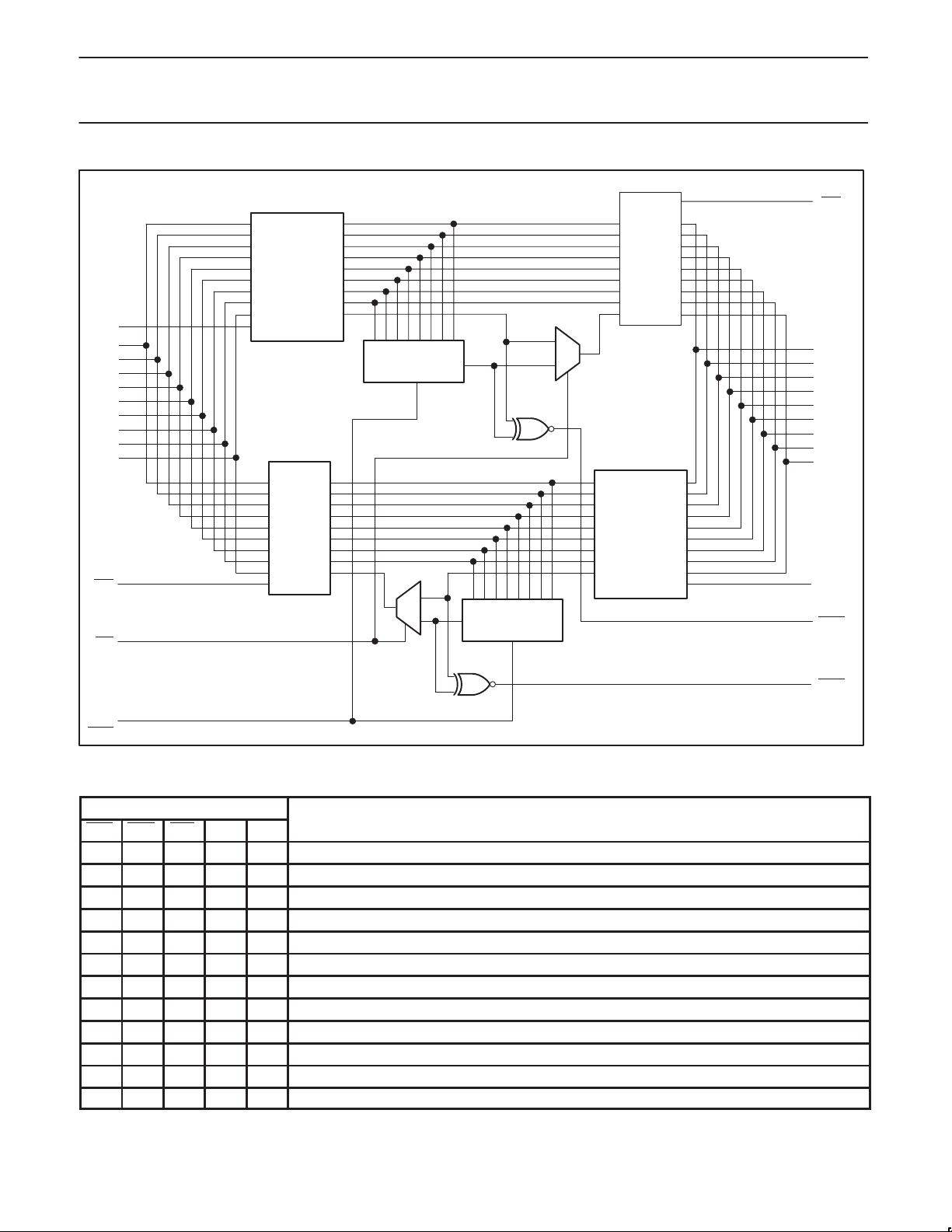
9–bit
Transparent
Latch
3
LEA
APAR
4
A0
5
A1
6
A2
7
A3
8
A4
9
A5
10
A6
11
A7
12
LE
Parity
Generator
9–bit
Output
Buffer
1
mux
0
9–bit
Output
Buffer
9–bit
Transparent
Latch
OE
74ABT899
27
OEB
26
B0
25
B1
24
B2
23
B3
22
B4
21
B5
20
B6
19
B7
18
BPAR
13
OEA
SEL
ODD/
EVEN
16
1
OE
mux
1
0
Parity
Generator
LE
FUNCTION TABLE
INPUTS OPERATING MODE
OEB OEA SEL LEA LEB
H H X X X 3-State A bus and B bus (input A & B simultaneously)
H L L L H B → A, transparent B latch, generate parity from B0 - B7, check B bus parity
H L L H H B → A, transparent A & B latch, generate parity from B0 - B7, check A & B bus parity
H L L X L B → A, B bus latched, generate parity from latched B0 - B7 data, check B bus parity
H L H X H B → A, transparent B latch, parity feed-through, check B bus parity
H L H H H B → A, transparent A & B latch, parity feed-through, check A & B bus parity
L H L H X A → B, transparent A latch, generate parity from A0 - A7, check A bus parity
L H L H H A → B, transparent A & B latch, generate parity from A0 - A7, check A & B bus parity
L H L L X A → B, A bus latched, generate parity from latched A0 - A7 data, check A bus parity
L H H H L A → B, transparent A latch, parity feed-through, check A bus parity
L H H H H A → B, transparent A & B latch, parity feed-through, check A & B bus parity
L L X X X Output to A bus and B bus (NOT ALLOWED)
H = High voltage level
L = Low voltage level
X = Don’t care
17
2
15
LEB
ERRA
ERRB
SA00292
1998 Jan 16
4

Philips Semiconductors Product specification
9-bit dual latch transceiver with 8-bit parity
generator/checker (3-State)
PARITY AND ERROR FUNCTION TABLE
INPUTS OUTPUTS
SEL ODD/EVEN
H H H
H H L
H L H
H L L
L H H
L H L
L L H
L L L
H = High voltage level
L = Low voltage level
t = Transmit–if the data path is from A→B then ERRt
r = Receive–if the data path is from A→B then ERRr is ERRB
* Blocked if latch is not transparent
xPAR
(A or B)
Σ of High
Inputs
Even
Odd
Even
Odd
Even
Odd
Even
Odd
Even
Odd
Even
Odd
Even
Odd
Even
Odd
xPAR
(B or A)
H
H
L
L
H
H
L
L
H
L
H
L
L
H
L
H
is ERRA
ERRt ERRr*
H
L
L
H
L
H
H
L
H
L
L
H
L
H
H
L
H
L Odd
L
H
L
H Even
H
L
H
H Odd
H
H
H
H Even
H
H
Mode
Mode
Mode
Mode
74ABT899
PARITY MODES
Feed-through/check parity
Generate parity
ABSOLUTE MAXIMUM RATINGS
SYMBOL
V
I
V
I
OK
V
OUT
I
OUT
T
NOTES:
1. Stresses beyond those listed may cause permanent damage to the device. These are stress ratings only and functional operation of the
device at these or any other conditions beyond those indicated under “recommended operating conditions” is not implied. Exposure to
absolute-maximum-rated conditions for extended periods may affect device reliability .
2. The performance capability of a high-performance integrated circuit in conjunction with its thermal environment can create junction
temperatures which are detrimental to reliability. The maximum junction temperature of this integrated circuit should not exceed 1505C.
3. The input and output voltage ratings may be exceeded if the input and output current ratings are observed.
DC supply voltage –0.5 to +7.0 V
CC
DC input diode current VI < 0 –18 mA
IK
DC input voltage
I
DC output diode current VO < 0 –50 mA
DC output voltage
DC output current output in Low state 128 mA
Storage temperature range –65 to 150 °C
stg
PARAMETER CONDITIONS RATING UNIT
3
3
1, 2
–1.2 to +7.0 V
output in Off or High state –0.5 to +5.5 V
1998 Jan 16
5
 Loading...