

Philips 74ABT863PW, 74ABT863N, 74ABT863DB, 74ABT863D Datasheet

INTEGRATED CIRCUITS
74ABT863
9-bit bus transceiver (3-State)
Product specification
Supersedes data of 1993 Jun 21
IC23 Data Handbook
1998 Jan 16

Philips Semiconductors Product specification
74ABT8639-bit bus transceiver (3-State)
FEA TURES
•Provides high performance bus interface buffering for wide
data/address paths or buses carrying parity
•Power-up 3-State
•Live insertion/extraction permitted
•Inputs are disabled during 3-State mode
•Buffered control inputs for light loading, or increased fan-in as
required with MOS microprocessors
•Output capability: +64mA/–32mA
•Latch-up protection exceeds 500mA per Jedec Std 17
•ESD protection exceeds 2000V per MIL STD 883 Method 3015
and 200 V per Machine Model
QUICK REFERENCE DATA
SYMBOL PARAMETER
t
PLH
t
PHL
C
IN
C
I/O
I
CCZ
ORDERING INFORMATION
24-Pin Plastic DIP –40°C to +85°C 74ABT863 N 74ABT863 N SOT222-1
24-Pin plastic SO –40°C to +85°C 74ABT863 D 74ABT863 D SOT137-1
24-Pin Plastic SSOP Type II –40°C to +85°C 74ABT863 DB 74ABT863 DB SOT340-1
24-Pin Plastic TSSOP Type I –40°C to +85°C 74ABT863 PW 74ABT863PW DH SOT355-1
Propagation delay
An to Bn or Bn to An
CL = 50pF; VCC = 5V 3.3 ns
Input capacitance VI = 0V or V
I/O capacitance Outputs disabled; VO = 0V or V
Total supply current Outputs disabled; VCC = 5.5V 110 µA
PACKAGES TEMPERATURE RANGE OUTSIDE NORTH AMERICA NORTH AMERICA DWG NUMBER
DESCRIPTION
The 74ABT863 bus transceiver provides high performance bus
interface buffering for wide data/address paths of buses carrying
parity.
The 74ABT863 9-bit bus transceiver has NOR-ed transmit and
receive output enables for maximum control flexibility.
CONDITIONS
T
= 25°C; GND = 0V
amb
CC
CC
TYPICAL UNIT
4 pF
7 pF
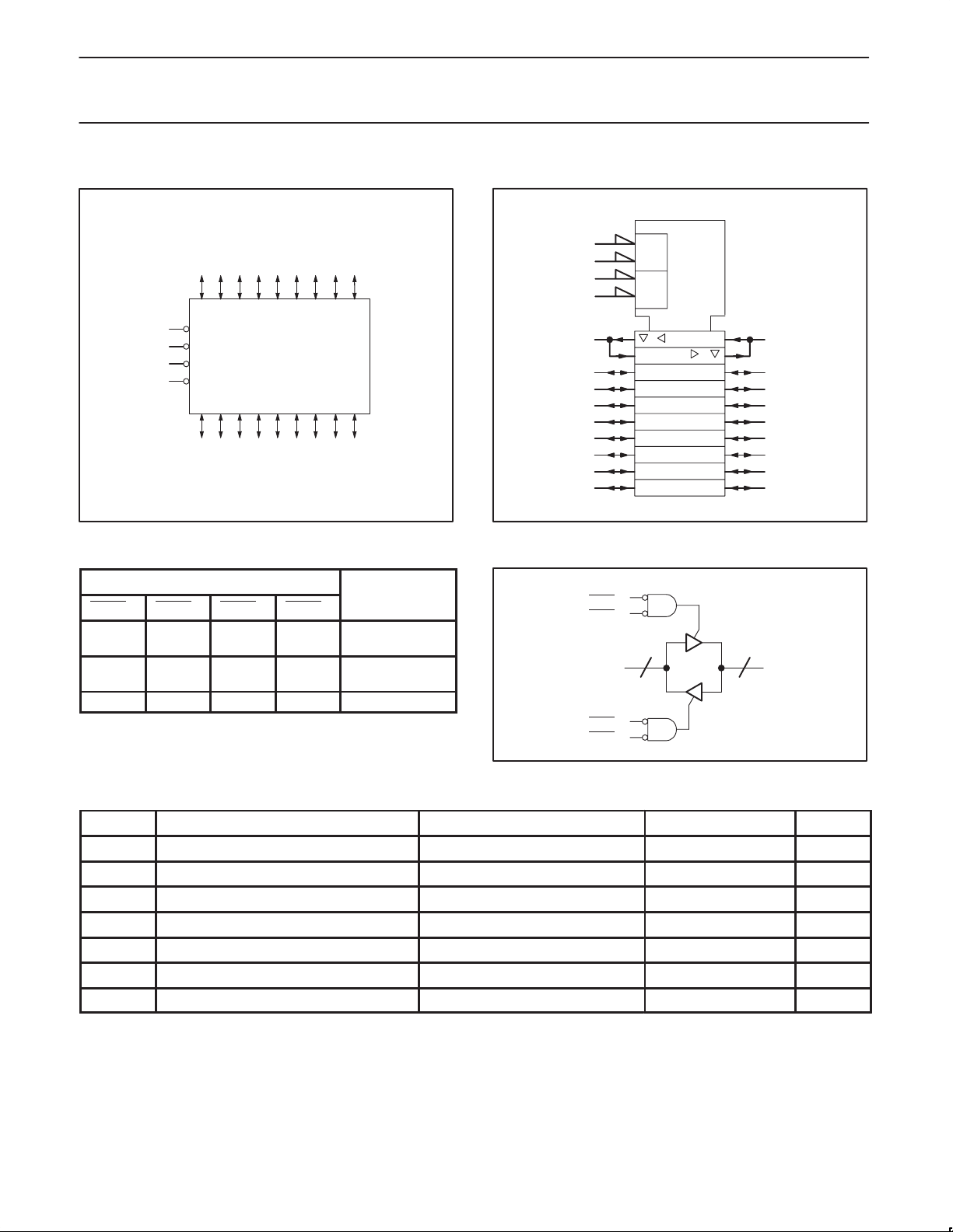
PIN CONFIGURATION
PIN DESCRIPTION
PIN NUMBER SYMBOL FUNCTION
14, 13 OEAB0, OEAB1
2, 3, 4, 5,
6, 7, 8, 9, 10
23, 22, 21, 20,
19, 18, 17, 16, 15
A0-A8
B0-B8
1, 11 OEBA0, OEBA1
12 GND Ground (0V)
24 V
CC
SA00283
24
V
CC
23
B0
22
B1
21
B2
20
B3
19
B4
18
B5
17
B6
16
B8
OEAB
0
OEAB
1
2
1
OEBA0
2
A0
3
A1
4
A2
5
A3
6
A4
TOP VIEW
7
A5
8
A6
9
A7 B7
10 15
A8
1
11 14OEBA
12 13GND
1998 Jan 16 853–1622 18869
Output enable inputs
(active-Low)
Data inputs/outputs (A
side)
Data inputs/outputs (B
side)
Output enable inputs
(active-Low)
Positive supply voltage
Philips Semiconductors Product specification
74ABT8639-bit bus transceiver (3-State)
LOGIC SYMBOL
2345678910
A0 A1 A2 A3 A4 A5 A6 A7 A8
1
OEBA0
11
OEBA1
14
OEAB0
13
OEAB1
B0 B1 B2 B3 B4 B5 B6 B7 B8
23 22 21 20 19 18 17 16 15
SA00284
FUNCTION TABLE
INPUTS OPERATING
OEAB0 OEAB1 OEBA0 OEBA1 MODE
L
L
H
X
H H H H Z
H = High voltage level
L = Low voltage level
X = Don’t care
Z = High impedance “off” state
L
L
X
H
H
X
L
L
X
H
L
L
A data to B bus
A data to B bus
B data to A bus
B data to A bus
LOGIC SYMBOL (IEEE/IEC)
1
11
14
13
223
322
421
520
619
718
817
916
10 15
&
EN1(BA)
&
EN2(AB)
1
LOGIC DIAGRAM
0
OEAB
OEAB1
An Bn
OEBA
0
OEBA
1
2
SA00285
99
SA00286
ABSOLUTE MAXIMUM RA TINGS
SYMBOL
V
CC
I
IK
V
I
I
OK
V
OUT
I
OUT
T
stg
DC supply voltage –0.5 to +7.0 V
DC input diode current VI < 0 –18 mA
DC input voltage
DC output diode current VO < 0 –50 mA
DC output voltage
DC output current output in Low state 128 mA
Storage temperature range –65 to 150 °C
PARAMETER CONDITIONS RATING UNIT
3
3
1, 2
–1.2 to +7.0 V
output in Off or High state –0.5 to +5.5 V
NOTES:
1. Stresses beyond those listed may cause permanent damage to the device. These are stress ratings only and functional operation of the
device at these or any other conditions beyond those indicated under “recommended operating conditions” is not implied. Exposure to
absolute-maximum-rated conditions for extended periods may affect device reliability .
2. The performance capability of a high-performance integrated circuit in conjunction with its thermal environment can create junction
temperatures which are detrimental to reliability. The maximum junction temperature of this integrated circuit should not exceed 150°C.
3. The input and output voltage ratings may be exceeded if the input and output current ratings are observed.
1998 Jan 16
3
Philips Semiconductors Product specification
74ABT8639-bit bus transceiver (3-State)
RECOMMENDED OPERATING CONDITIONS
SYMBOL PARAMETER LIMITS UNIT
Min Max
V
V
V
V
I
OH
I
OL
∆t/∆v Input transition rise or fall rate 0 5 ns/V
T
amb
DC ELECTRICAL CHARACTERISTICS
SYMBOL PARAMETER TEST CONDITIONS T
V
V
OH
V
OL
I
I
OFF
I
PU/PD
IIH + I
IIL + I
I
CEX
I
O
I
CCH
I
CCL
I
CCZ
∆I
CC
DC supply voltage 4.5 5.5 V
CC
Input voltage 0 V
I
High-level input voltage 2.0 V
IH
Low-level Input voltage 0.8 V
IL
CC
High-level output current –32 mA
Low-level output current 64 mA
Operating free-air temperature range –40 +85 °C
LIMITS
T
amb
= +25°C
amb
to +85°C
Min Typ Max Min Max
Input clamp voltage VCC = 4.5V; IIK = –18mA –0.9 –1.2 –1.2 V
IK
VCC = 4.5V; IOH = –3mA; VI = VIL or V
High-level output voltage VCC = 5.0V; IOH = –3mA; VI = VIL or V
VCC = 4.5V; IOH = –32mA; VI = VIL or V
Low-level output voltage VCC = 4.5V; IOL = 64mA; VI = VIL or V
Input leakage Control pins VCC = 5.5V; VI = GND or 5.5V ±0.01 ±1.0 ±1.0 µA
I
IH
IH
IH
IH
2.5 3.2 2.5 V
3.0 3.7 3.0 V
2.0 2.3 2.0 V
0.42 0.55 0.55 V
current Data pins VCC = 5.5V; VI = GND or 5.5V ±5 ±100 ±100 µA
Power-off leakage current VCC = 0.0V; VO or VI ≤ 4.5V ±5.0 ±100 ±100 µA
Power-up/down 3-State
output current
3-State output High current VCC = 5.5V; VO = 2.7V; VI = VIL or V
OZH
3-State output Low current VCC = 5.5V; VO = 0.5V; VI = VIL or V
OZL
3
Output high leakage current VCC = 5.5V; VO = 5.5V; VI = GND or V
Output current
1
Quiescent supply current VCC = 5.5V; Outputs Low, VI = GND or V
Additional supply current per
input pin
2
VCC = 2.0V; VO = 0.5V; VI = GND or VCC; =
VOE= Don’t care
IH
IH
CC
±5.0 ±50 ±50 µA
5.0 50 50 µA
–5.0 –50 –50 µA
5.0 50 50 µA
VCC = 5.5V; VO = 2.5V –50 –63 –180 –50 –180 mA
VCC = 5.5V; Outputs High, VI = GND or V
VCC = 5.5V; Outputs 3–State;
VI = GND or V
CC
Outputs enabled, one input at 3.4V ,
other inputs at VCC or GND; VCC = 5.5V
Outputs 3-State, one data input at 3.4V ,
other inputs at VCC or GND; VCC = 5.5V
Outputs 3-State, one enable input at 3.4V ,
other inputs at VCC or GND; VCC = 5.5V
CC
CC
110 250 250 µA
25 38 38 mA
110 250 250 µA
0.5 1.5 1.5 mA
110 250 250 µA
0.5 1.5 1.5 mA
= –40°C
V
UNIT
NOTES:
1. Not more than one output should be tested at a time, and the duration of the test should not exceed one second.
2. This is the increase in supply current for each input at 3.4V .
3. This parameter is valid for any VCC between 0V and 2.1V , with a transition time of up to 10msec. From VCC = 2.1V to VCC = 5V ± 10%, a
transition time of up to 100µsec is permitted.
1998 Jan 16
4
 Loading...