

Philips 74ABT861PW, 74ABT861N, 74ABT861DB, 74ABT861D Datasheet

INTEGRATED CIRCUITS
74ABT861
10-bit bus transceiver (3-State)
Product specification
Supersedes data of 1995 Sep 06
IC23 Data Handbook
1998 Jan 16
Philips Semiconductors Product specification
74ABT86110-bit bus transceiver (3-State)
FEA TURES
•Provides high performance bus interface buffering for wide
data/address paths or buses carrying parity
•Buffered control inputs for light loading, or increased fan-in as
required with MOS microprocessors
•Output capability: +64mA/–32mA
•Latch-up protection exceeds 500mA per Jedec Std 17
•ESD protection exceeds 2000 V per MIL STD 883 Method 3015
and 200 V per Machine Model
•Power-up 3-State
•Inputs are disabled during 3-State mode
QUICK REFERENCE DATA
SYMBOL PARAMETER
t
PLH
t
PHL
C
C
I
CCZ
IN
I/O
Propagation delay
An to Bn or Bn to An
Input capacitance VI = 0V or V
I/O capacitance Outputs disabled; VO = 0V or V
Total supply current Outputs disabled; VCC =5.5V 500 nA
DESCRIPTION
The 74ABT861 bus transceiver provides high performance bus
interface buffering for wide data/address paths of buses carrying
parity.
The 74ABT861 10-bit bus transceiver has NOR-ed transmit and
receive output enables for maximum control flexibility.
CONDITIONS
T
= 25°C; GND = 0V
amb
CL = 50pF; VCC = 5V 3.4 ns
CC
CC
TYPICAL UNIT
4 pF
7 pF
ORDERING INFORMATION
PACKAGES TEMPERATURE RANGE OUTSIDE NORTH AMERICA NORTH AMERICA DWG NUMBER
24-Pin Plastic DIP –40°C to +85°C 74ABT861 N 74ABT861 N SOT222-1
24-Pin plastic SO –40°C to +85°C 74ABT861 D 74ABT861 D SOT137-1
24-Pin Plastic SSOP Type II –40°C to +85°C 74ABT861 DB 74ABT861 DB SOT340-1
24-Pin Plastic TSSOP Type I –40°C to +85°C 74ABT861 PW 74ABT861PW DH SOT355-1
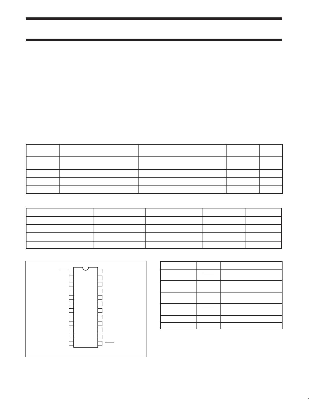
PIN CONFIGURATION
1
OEBA
2
A0
3
A1
4
A2
5
A3
6
A4
7
A5
8
A6
9
A7 B7
10 15
A8
11 14A9
12 13GND
TOP VIEW
24
V
CC
23
B0
22
B1
21
B2
20
B3
19
B4
18
B5
17
B6
16
B8
B9
OEAB
PIN DESCRIPTION
PIN NUMBER SYMBOL FUNCTION
13 OEAB
2, 3, 4, 5, 6,
7, 8, 9, 10, 11
23, 22, 21, 20, 19,
18, 17, 16, 15, 14
A0-A9 Data inputs/outputs (A side)
B0-B9 Data inputs/outputs (B side)
1 OEBA
12 GND Ground (0V)
24 V
A side to B side output enable
input (active-Low)
B side to A side output enable
input (active-Low)
Positive supply voltage
CC
SA00278
1998 Jan 16 853-1621 18866
2

Philips Semiconductors Product specification
74ABT86110-bit bus transceiver (3-State)
LOGIC SYMBOL
2345 6789
A0 A1 A2 A3 A4 A5 A6 A7
1
OEBA
13
OEAB
B0 B1 B2 B3 B4 B5 B6 B7
23 22 21 20 19 18 17 16
LOGIC DIAGRAM
OEAB
OEBA
10 11
A8 A9
B8 B9
15 14
SA00279
1010
An Bn
SA00281
LOGIC SYMBOL (IEEE/IEC)
1
EN1(BA)
13
EN2(AB)
223
322
421
520
619
718
817
916
10 15
11 14
1
2
SA00280
FUNCTION TABLE
INPUTS OPERATING
OEAB OEBA MODE
L H A data to B bus
H L B data to A bus
H H Z
H = High voltage level
L = Low voltage level
X = Don’t care
Z = High impedance “off” state
ABSOLUTE MAXIMUM RATINGS
SYMBOL
V
CC
I
IK
V
I
I
OK
V
OUT
I
OUT
T
stg
DC supply voltage –0.5 to +7.0 V
DC input diode current VI < 0 –18 mA
DC input voltage
DC output diode current VO < 0 –50 mA
DC output voltage
DC output current output in Low state 128 mA
Storage temperature range –65 to 150 °C
PARAMETER CONDITIONS RATING UNIT
3
3
1, 2
–1.2 to +7.0 V
output in Off or High state –0.5 to +5.5 V
NOTES:
1. Stresses beyond those listed may cause permanent damage to the device. These are stress ratings only and functional operation of the
device at these or any other conditions beyond those indicated under “recommended operating conditions” is not implied. Exposure to
absolute-maximum-rated conditions for extended periods may affect device reliability .
2. The performance capability of a high-performance integrated circuit in conjunction with its thermal environment can create junction
temperatures which are detrimental to reliability. The maximum junction temperature of this integrated circuit should not exceed 150°C.
3. The input and output voltage ratings may be exceeded if the input and output current ratings are observed.
1998 Jan 16
3
 Loading...