

Philips 74ABT853PW, 74ABT853N, 74ABT853DB, 74ABT853D Datasheet
Philips Semiconductors Product specification
8-bit transceiver with 9-bit parity checker/
generator and flag latch (3-State)
FEA TURES
•Low static and dynamic power dissipation with high speed and
high output drive
•Open-collector ERROR output
•Output capability: +64mA/–32mA
•Latch-up protection exceeds 500mA per Jedec Std 17
•ESD protection exceeds 2000 V per MIL STD 883 Method 3015
and 200 V per Machine Model
•Power-up 3-State
•Live insertion/extraction permitted
DESCRIPTION
The 74ABT853 high-performance BiCMOS device combines low
static and dynamic power dissipation with high speed and high
output drive.
QUICK REFERENCE DATA
SYMBOL PARAMETER
t
PLH
t
PHL
t
PLH
t
PHL
C
C
I
CCZ
IN
I/O
Propagation delay
An to Bn or Bn to An
Propagation delay
An to PARITY
Input capacitance VI = 0V or V
I/O capacitance Outputs disabled; VO = 0V or V
Total supply current Outputs disabled; VCC =5.5V 50 µA
74ABT853
The 74ABT853 is an octal transceiver with a parity
generator/checker and is intended for bus–oriented applications.
When Output Enable A (OEA
high impedance state. Output Enable B (OEB
outputs in the same way.
The parity generator creates an odd parity output (PARITY) when
OEB
is Low. When OEA is Low, the parity of the B port, including
the PARITY input, is checked for odd parity. When an error is
detected, the error data is sent to the input of a latch. The error data
can then be passed, stored, cleared, or sampled depending on the
ENABLE
If both OEA
and CLEAR control signals.
and OEB are Low, data will flow from the A bus to the B
bus and the part is forced into an error condition which creates an
inverted PARITY output. This error condition can be used by the
designer for system diagnostics.
CONDITIONS
= 25°C; GND = 0V
T
amb
CL = 50pF; VCC = 5V 3.4 ns
CL = 50pF; VCC = 5V 7.4 ns
CC
) is High, it will place the A outputs in a
) controls the B
TYPICAL UNIT
4 pF
CC
7 pF
ORDERING INFORMATION
PACKAGES TEMPERATURE RANGE OUTSIDE NORTH AMERICA NORTH AMERICA DWG NUMBER
24-Pin Plastic DIP –40°C to +85°C 74ABT853 N 74ABT853 N SOT222-1
24-Pin plastic SO –40°C to +85°C 74ABT853 D 74ABT853 D SOT137-1
24-Pin Plastic SSOP Type II –40°C to +85°C 74ABT853 DB 74ABT853 DB SOT340-1
24-Pin Plastic TSSOP Type I –40°C to +85°C 74ABT853 PW 74ABT853PW DH SOT355-1
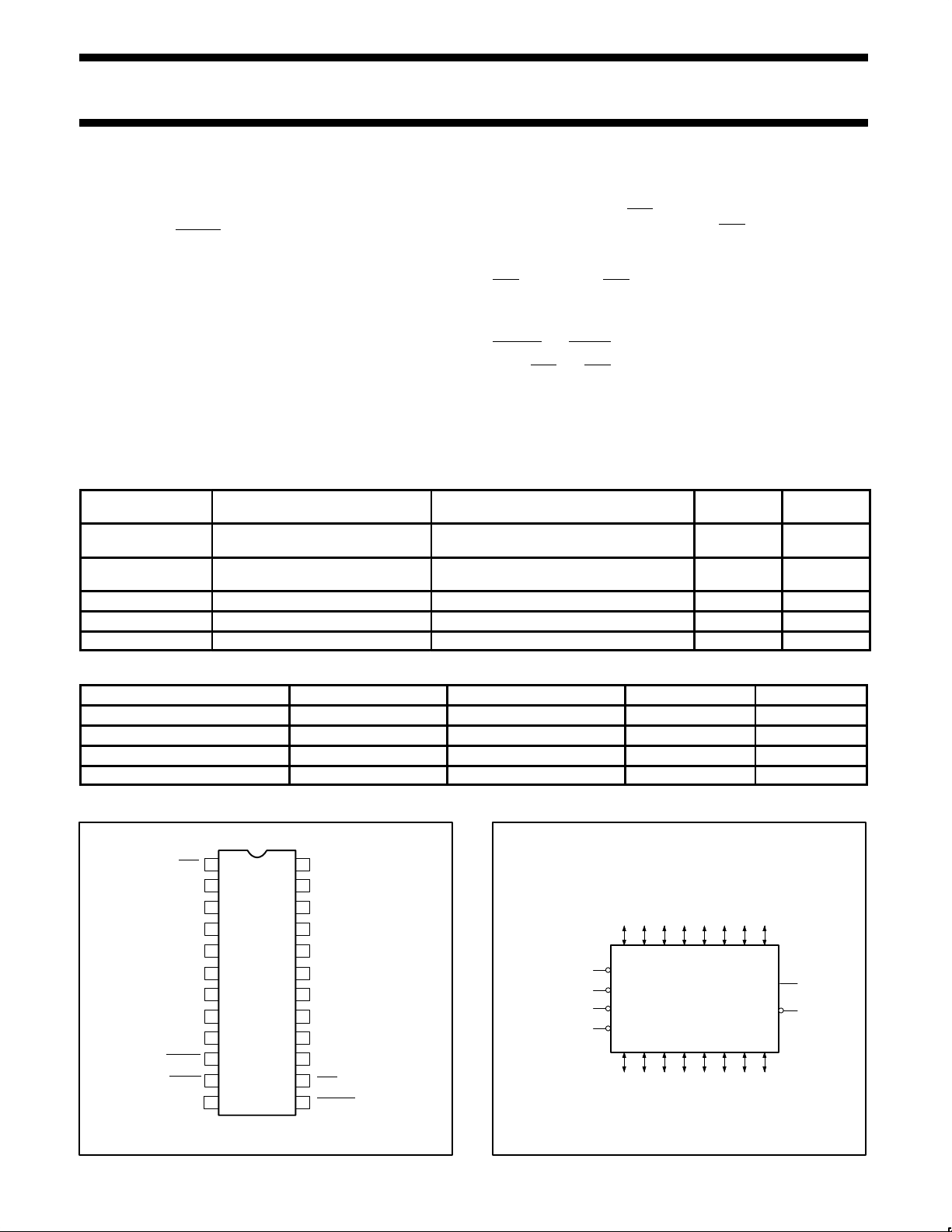
PIN CONFIGURA TION
1
OEA
2
A0
3
A1
4
A2
5
A3
6
A4
A5
7
8
A6
9
A7
10
ERROR
11
CLEAR
GND
24
23
22
21
20
19
18
17
16
15
14
1312
V
CC
B0
B1
B2
B3
B4
B5
B6
B7
PARITY
OEB
ENABLE
LOGIC SYMBOL
14
1
11
23456789
A0 A1 A2 A3 A4 A5 A6 A7
OEB
OEA
CLEAR
ENABLE13
B0 B1 B2 B3
23 22 21 20 19 18 17 16
PARITY
ERROR
B4 B5 B6 B7
15
10
TOP VIEW
1995 Sep 06 853-1672 15702
SA00262
1
SA00263
Philips Semiconductors Product specification
8-bit transceiver with 9-bit parity checker/
generator and flag latch (3-State)
PIN DESCRIPTION
SYMBOL PIN NUMBER NAME AND FUNCTION
A0 – A7 2, 3, 4, 5, 6, 7, 8, 9 A port 3–State inputs/outputs
B0 – B7 23, 22, 21, 20, 19, 18, 17, 16 B port 3–State inputs/outputs
OEA 1 Enables the A outputs when Low
OEB 14 Enables the B outputs when Low
PARITY 15 Parity output/input
ERROR 10 Error output (open collector)
CLEAR 11 Clears the error flag register when Low
ENABLE 13 Enable input (active-Low)
GND 12 Ground (0V)
V
CC
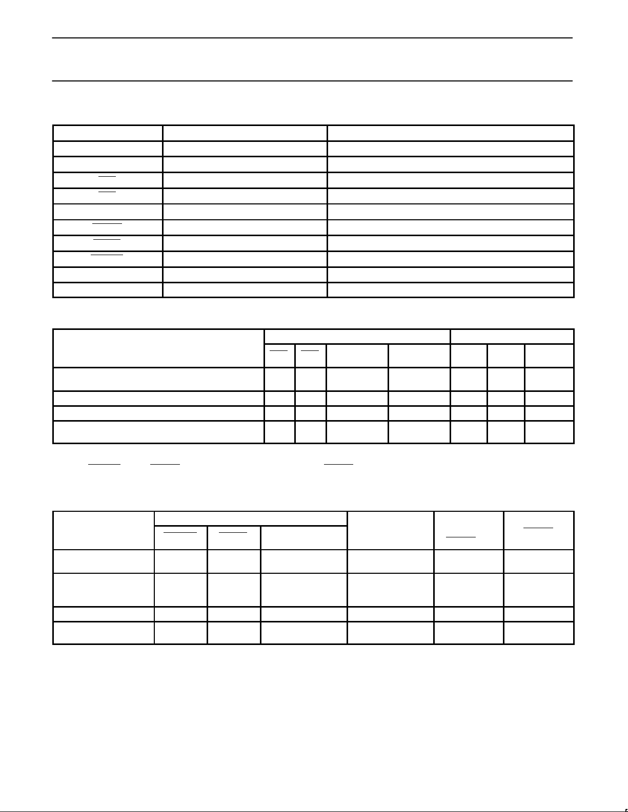
FUNCTION TABLE
MODE OEB OEA
A data to B bus and generate odd parity output L H
B data to A bus and check for parity error
A bus and B bus disabled
A data to B bus and generate inverted parity output L L
NOTES:
1. Error checking is detailed in the Error Flag Function Table below.
2. When ENABLE
2
is Low, ERROR is Low if the sum of A inputs is even or ERROR is High if the sum of A inputs is odd.
1
24 Positive supply voltage
H L (output) X Bn (input) (input)
H H X X Z Z Z
74ABT853
INPUTS OUTPUTS
An
Σ OF HIGHS
Odd
Even
Odd
Even
Bn + PARITY
Σ OF HIGHS
(output) (input) An
(output) (input) An
An Bn PARITY
L
H
H
L
ERROR FLAG FUNCTION TABLE
MODE ENABLE CLEAR
Pass L L
Sample L H
Clear H L X X X H
Store H H X X
H = High voltage level steady state
L = Low voltage level steady state
X = Don’t care
Z = High impedance ”off” state
1995 Sep 06
INPUTS INTERNAL NODE OUTPUT
Bn + PARITY
Σ OF HIGHS
Odd
Even
Odd
Even
X
2
POINT ”P”
H
L
H
L
X
PRE–STATE
ERROR
X
H
X
L
L
H
n–1
ERROR
OUTPUT
H
L
H
L
L
L
H
Philips Semiconductors Product specification
8-bit transceiver with 9-bit parity checker/
generator and flag latch (3-State)
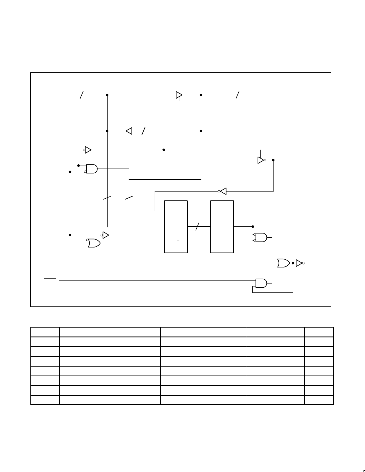
LOGIC DIAGRAM
8 8
A0 – A7
8
OEB
OEA
88
}
}
Sel A/B
MUX
B
A
74ABT853
B0 – B7
PARITY
9–bit
Odd
Parity
9
Tree
”P”
ERROR
ENABLE
CLEAR
SA00264
ABSOLUTE MAXIMUM RATINGS
SYMBOL
V
CC
I
IK
V
I
I
OK
V
OUT
I
OUT
T
stg
DC supply voltage –0.5 to +7.0 V
DC input diode current VI < 0 –18 mA
DC input voltage
DC output diode current VO < 0 –50 mA
DC output voltage
DC output current output in Low state 128 mA
Storage temperature range –65 to 150 °C
PARAMETER CONDITIONS RATING UNIT
3
3
1, 2
–1.2 to +7.0 V
output in Off or High state –0.5 to +5.5 V
NOTES:
1. Stresses beyond those listed may cause permanent damage to the device. These are stress ratings only and functional operation of the
device at these or any other conditions beyond those indicated under “recommended operating conditions” is not implied. Exposure to
absolute-maximum-rated conditions for extended periods may affect device reliability .
2. The performance capability of a high-performance integrated circuit in conjunction with its thermal environment can create junction
temperatures which are detrimental to reliability. The maximum junction temperature of this integrated circuit should not exceed 150°C.
3. The input and output voltage ratings may be exceeded if the input and output current ratings are observed.
1995 Sep 06
3
 Loading...