

Philips 74ABT845N, 74ABT845DB, 74ABT845D, 74ABT845PW Datasheet
Philips Semiconductors Product specification
8-bit bus interface latch with set and reset
(3-State)
FEA TURES
•High speed parallel latches
•Ideal where high speed, light loading, or increased fan-in are
required with MOS microprocessors
•Broadside pinout
•Output capability: +64mA/–32mA
•Power-up 3-State
•Power-up reset
•Latch-up protection exceeds 500mA per Jedec Std 17
•ESD protection exceeds 2000 V per MIL STD 883 Method 3015
and 200 V per Machine Model
QUICK REFERENCE DAT A
SYMBOL PARAMETER
C
t
PLH
t
PHL
C
OUT
I
CCZ
IN
Propagation delay
Dn to Qn
CL = 50pF; VCC = 5V 5.4 ns
Input capacitance VI = 0V or V
Output capacitance
Outputs disabled;
= 0V or V
V
O
Total supply current Outputs disabled; VCC = 5.5V 500 nA
74ABT845
DESCRIPTION
The 74ABT845 consists of eight D-type latches with 3-State outputs.
In addition to the LE, OE
additional OE
OE
1, OE2) pins. The multiple Output enables allow multiuser control
pins, making a total of three Output Enable (OE0,
of the interface, e.g., CS
CONDITIONS
= 25°C; GND = 0V
T
amb
CC
CC
, MR and PRE pins, the 74ABT845 has two
, DMA, and RD/WR.
TYPICAL UNIT
4 pF
7 pF
ORDERING INFORMATION
PACKAGES TEMPERATURE RANGE OUTSIDE NORTH AMERICA NORTH AMERICA DWG NUMBER
24-Pin Plastic DIP –40°C to +85°C 74ABT845 N 74ABT845 N SOT222-1
24-Pin plastic SO –40°C to +85°C 74ABT845 D 74ABT845 D SOT137-1
24-Pin Plastic SSOP Type II –40°C to +85°C 74ABT845 DB 74ABT845 DB SOT340-1
24-Pin Plastic TSSOP Type I –40°C to +85°C 74ABT845 PW 74ABT845PW DH SOT355-1
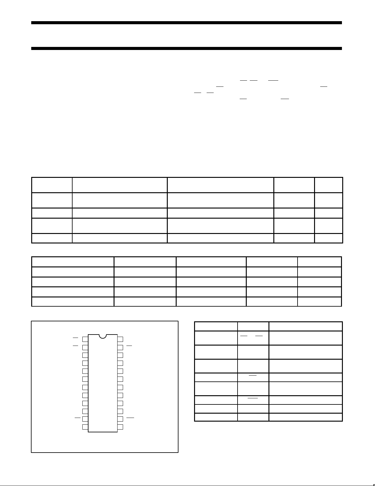
PIN CONFIGURA TION
1
OE0
2
OE1
3
D0
4
D1
5
D2
6
D3
7
D4
8
D5
9
D6 Q6
10 15
D7
11 14MR
12 13GND
24
V
CC
OE
23
2
Q0
22
Q1
21
Q2
20
Q3
19
Q4
18
Q5
17
16
Q7
PRE
LE
PIN DESCRIPTION
PIN NUMBER SYMBOL FUNCTION
1, 2, 23 OE0 – OE2
3, 4, 5, 6,
7, 8, 9, 10
22, 21, 20, 19,18,
17, 16, 15
D0-D7 Data inputs
Q0-Q7 Data outputs
11 MR Master reset input (active-Low)
13 LE
14 PRE Preset input (active-Low)
12 GND Ground (0V)
24 V
CC
Output enable inputs
(active-Low)
Latch enable input
(active-High)
Positive supply voltage
TOP VIEW
SA00258
1995 Sep 06 853-1703 15702
1
Philips Semiconductors Product specification
8-bit bus interface latch with set and reset
(3-State)
LOGIC SYMBOL (IEEE/IEC)
&
1
2
23
14
11
13
3
4
5
6
7
8
9
10
EN
S2
R
C1
21D
22
21
20
19
18
17
16
15
SA00260
LOGIC SYMBOL
13
LE
14
PRE
11
MR
1
OE0
2 OE1
23 OE2
74ABT845
345678910
D0 D1 D2 D3 D4 D5 D6 D7
Q0 Q1 Q2 Q3 Q4 Q5 Q6 Q7
22 21 20 19 18 17 16 15
SA00259
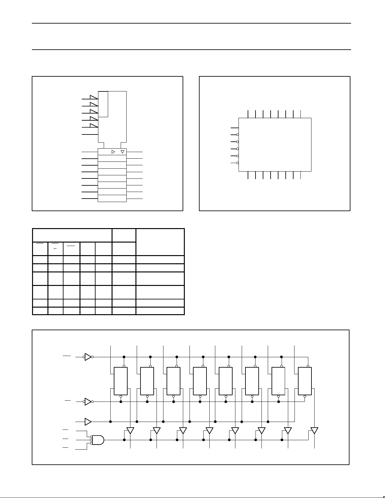
FUNCTION TABLE
OUTPU
TS
OEnPR
E
INPUTS
MR LE Dn Qn
L L X X X H Preset
L H L X X L Clear
LLHHHHH
LLHHH
H
HLH
↓
↓
l
h
L
H
L
H
H X X X X Z High impedance
L H H L X NC Hold
OPERATING
MODE
Transparent
Latched
LOGIC DIAGRAM
PRE
MR
D0
14
11
3
D
LQ
D1
4
PPPPPPPP
D
C C C C C C C C
LQ
D2
5
D
LQ
H = High voltage level
h = High voltage level one set-up time prior to the High-to-Low LE
transition
L = Low voltage level
l = Low voltage level one set-up time prior to the High-to-Low LE
transition
NC= No change
X = Don’t care
Z = High impedance “off” state
↓ = High-to-Low transition
D3
6
D
LQ
D4
7
D
LQ
D5
8
D
LQ
D6
9
D
LQ
D7
10
D
LQ
1995 Sep 06
OE0
OE
OE2
13
LE
1
2
1
23
Q0
22
Q1
21
Q2
20
Q3
19
Q4
18
Q5
17
16
Q6
15
Q7
SA00261
2
Philips Semiconductors Product specification
8-bit bus interface latch with set and reset
(3-State)
ABSOLUTE MAXIMUM RATINGS
SYMBOL
V
I
V
I
V
I
OK
OUT
OUT
T
DC supply voltage –0.5 to +7.0 V
CC
DC input diode current VI < 0 –18 mA
IK
DC input voltage
I
DC output diode current VO < 0 –50 mA
DC output voltage
DC output current output in Low state 128 mA
Storage temperature range –65 to 150 °C
stg
NOTES:
1. Stresses beyond those listed may cause permanent damage to the device. These are stress ratings only and functional operation of the
device at these or any other conditions beyond those indicated under “recommended operating conditions” is not implied. Exposure to
absolute-maximum-rated conditions for extended periods may affect device reliability .
2. The performance capability of a high-performance integrated circuit in conjunction with its thermal environment can create junction
temperatures which are detrimental to reliability. The maximum junction temperature of this integrated circuit should not exceed 150°C.
3. The input and output voltage ratings may be exceeded if the input and output current ratings are observed.
PARAMETER CONDITIONS RATING UNIT
3
3
RECOMMENDED OPERATING CONDITIONS
SYMBOL PARAMETER LIMITS UNIT
V
V
V
V
I
OH
I
OL
∆t/∆v Input transition rise or fall rate 0 5 ns/V
T
amb
DC supply voltage 4.5 5.5 V
CC
Input voltage 0 V
I
High-level input voltage 2.0 V
IH
Low-level input voltage 0.8 V
IL
High-level output current –32 mA
Low-level output current 64 mA
Operating free-air temperature range –40 +85 °C
1,2
–1.2 to +7.0 V
output in Off or High state –0.5 to +5.5 V
Min Max
74ABT845
CC
V
1995 Sep 06
3
 Loading...