

Philips 74abt843 DATASHEETS

INTEGRATED CIRCUITS
74ABT843
9-bit interface latch with set and reset
(3-State)
Product specification
Supersedes data of 1995 Sep 06
IC23 Data Handbook
1998 Jan 16
Philips Semiconductors Product specification
9-bit bus interface latch with set and reset
(3-State)
FEA TURES
•High speed parallel latches
•Extra data width for wide address/data paths or buses carrying
parity
•Ideal where high speed, light loading, or increased fan-in are
required with MOS microprocessors
•Slim DIP 300 mil package
•Broadside pinout
•Output capability: +64mA/–32mA
•Latch-up protection exceeds 500mA per Jedec Std 17
•ESD protection exceeds 2000V per MIL STD 883 Method 3015
and 200V per Machine Model
•Power-up 3-State
•Power-up reset
QUICK REFERENCE DATA
SYMBOL PARAMETER
C
t
PLH
t
PHL
C
OUT
I
CCZ
IN
Propagation delay
Dn to Qn
CL = 50pF; VCC = 5V 5.0 ns
Input capacitance VI = 0V or V
Output capacitance
Outputs disabled;
VO = 0V or V
Total supply current Outputs disabled; VCC = 5.5V 500 nA
74ABT843
DESCRIPTION
The 74ABT843 Bus interface latch is designed to eliminate the extra
packages required to buffer existing registers and provide extra data
width for wider data/address paths of buses carrying parity.
The 74ABT843 consists of nine D-type latches with 3-State outputs.
In addition to the LE and OE
and Preset (PRE
) pin. These pins are ideal for parity bus interfacing
in high performance systems. When MR
if OE
is Low. When MR is High, data can be entered into the latch.
When PRE
is Low, the outputs are High, if OE is Low. PRE
overrides MR.
CONDITIONS
T
= 25°C; GND = 0V
amb
CC
CC
pins, it has a Master Reset (MR) pin
is Low, the outputs are Low
TYPICAL UNIT
4 pF
7 pF
ORDERING INFORMATION
PACKAGES TEMPERATURE RANGE OUTSIDE NORTH AMERICA NORTH AMERICA DWG NUMBER
24-Pin Plastic DIP –40°C to +85°C 74ABT843 N 74ABT843 N SOT222-1
24-Pin plastic SO –40°C to +85°C 74ABT843 D 74ABT843 D SOT137-1
24-Pin Plastic SSOP Type II –40°C to +85°C 74ABT843 DB 74ABT843 DB SOT340-1
24-Pin Plastic TSSOP Type I –40°C to +85°C 74ABT843 PW 74ABT843PW DH SOT355-1
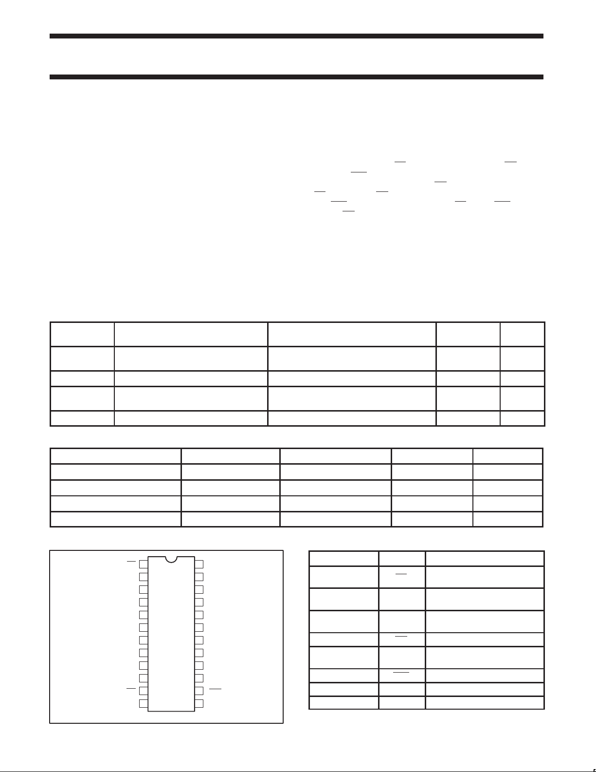
PIN CONFIGURATION
OE
D0
D1
D2
D3
D4
D5
D6
D7 Q7
10 15
D8
11 14MR
12 13GND
1
2
3
4
5
6
7
8
9
TOP VIEW
24
V
23
Q0
22
Q1
21
Q2
20
Q3
19
Q4
18
Q5
17
Q6
16
Q8
PRE
LE
SA00250
CC
PIN DESCRIPTION
PIN NUMBER SYMBOL FUNCTION
1 OE
2, 3, 4, 5, 6,
7, 8, 9, 10
23, 22, 21, 20,
19,18, 17, 16, 15
D0-D8 Data inputs
Q0-Q8 Data outputs
11 MR Master reset input (active-Low)
13 LE
14 PRE Preset input (active-Low)
12 GND Ground (0V)
24 V
CC
Output enable input
(active-Low)
Latch enable input (active rising
edge)
Positive supply voltage
1998 Jan 16 853-1620 18864
2
Philips Semiconductors Product specification
9-bit bus interface latch with set and reset
(3-State)
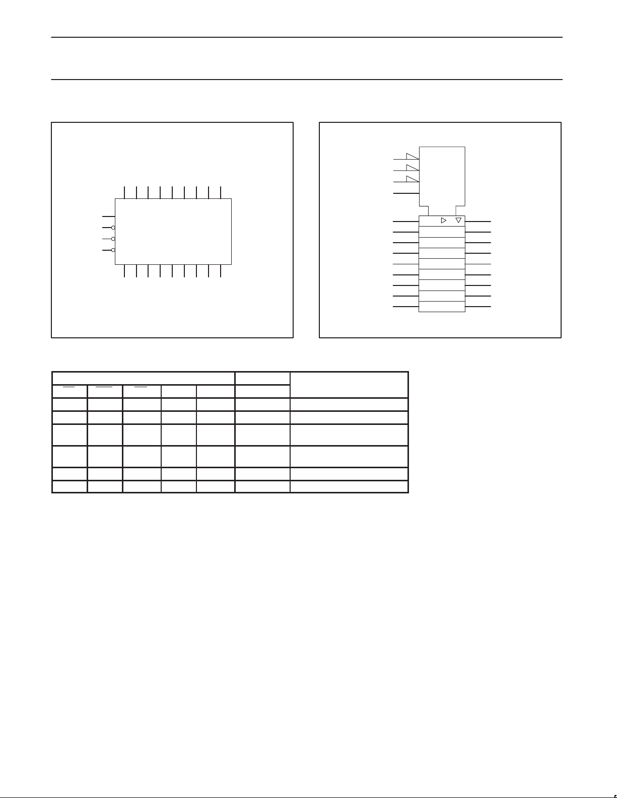
LOGIC SYMBOL
2345678910
D0 D1 D2 D3 D4 D5 D6 D7 D8
13
LE
14
PRE
11
MR
1
OE
Q0 Q1 Q2 Q3 Q4 Q5 Q6 Q7 Q8
23 22 21 20 19 18 17 16 15
SA00251
LOGIC SYMBOL (IEEE/IEC)
1
EN
11
R
14
S2
13
C1
223
1D
322
421
520
619
718
817
916
10 15
74ABT843
SA00252
FUNCTION TABLE
INPUTS OUTPUTS OPERATING MODE
OE PRE MR LE Dn Qn
L L X X X H Preset
L H L X X L Clear
L
L
L
L
H X X X X Z High impedance
L H H L X NC Hold
H = High voltage level
h = High voltage level one set-up time prior to the High-to-Low LE transition
L = Low voltage level
l = Low voltage level one set-up time prior to the High-to-Low LE transition
NC= No change
X = Don’t care
Z = High impedance “off” state
↓ = High-to-Low transition
H
H
H
H
H
H
H
H
H
H
↓
↓
L
H
l
h
L
H
L
H
Transparent
Latched
1998 Jan 16
3

Philips Semiconductors Product specification
9-bit bus interface latch with set and reset
(3-State)
LOGIC DIAGRAM
PRE
MR
OE
D0
14
11
13
LE
1
2
D1
3
PPPPPPPPP
D
LQ
C
D
LQ
23
Q0
D2
4
D
C C C C C C C C
LQ
22
Q1
D3
5
D
LQ
21
Q2
Q3
20
D4
6
D
LQ
Q4
D5
19
7
D
LQ
Q5
18
D6
8
D
LQ
Q6
17
D7
9
D
LQ
74ABT843
D8
10
D
LQ
16
Q7
Q8
SA00253
15
ABSOLUTE MAXIMUM RA TINGS
SYMBOL
V
CC
I
IK
V
I
I
OK
V
OUT
I
OUT
T
stg
DC supply voltage –0.5 to +7.0 V
DC input diode current VI < 0 –18 mA
DC input voltage
DC output diode current VO < 0 –50 mA
DC output voltage
DC output current output in Low state 128 mA
Storage temperature range –65 to 150 °C
PARAMETER CONDITIONS RATING UNIT
3
3
1, 2
–1.2 to +7.0 V
output in Off or High state –0.5 to +5.5 V
NOTES:
1. Stresses beyond those listed may cause permanent damage to the device. These are stress ratings only and functional operation of the
device at these or any other conditions beyond those indicated under “recommended operating conditions” is not implied. Exposure to
absolute-maximum-rated conditions for extended periods may affect device reliability .
2. The performance capability of a high-performance integrated circuit in conjunction with its thermal environment can create junction
temperatures which are detrimental to reliability. The maximum junction temperature of this integrated circuit should not exceed 150°C.
3. The input and output voltage ratings may be exceeded if the input and output current ratings are observed.
1998 Jan 16
4
Philips Semiconductors Product specification
9-bit bus interface latch with set and reset
(3-State)
RECOMMENDED OPERATING CONDITIONS
SYMBOL PARAMETER LIMITS UNIT
Min Max
V
CC
V
V
V
I
OH
I
OL
∆t/∆v Input transition rise or fall rate 0 10 ns/V
T
amb
DC ELECTRICAL CHARACTERISTICS
SYMBOL PARAMETER TEST CONDITIONS T
V
IK
V
OH
V
OL
V
RST
I
I
OFF
I
PU/IPD
I
OZH
I
OZL
I
CEX
I
O
I
CCH
I
CCL
I
CCZ
∆I
CC
NOTES:
1. Not more than one output should be tested at a time, and the duration of the test should not exceed one second.
2. This is the increase in supply current for each input at 3.4V.
3. For valid test results, data must not be loaded into the flip–flops (or latches) after applying the power.
4. This parameter is valid for any V
transition time of up to 100µsec is permitted.
DC supply voltage 4.5 5.5 V
Input voltage 0 V
I
High-level input voltage 2.0 V
IH
Low-level input voltage 0.8 V
IL
High-level output current –32 mA
Low-level output current 64 mA
Operating free-air temperature range –40 +85 °C
LIMITS
= +25°C
amb
Min Typ Max Min Max
Input clamp voltage VCC = 4.5V; IIK = –18mA –0.9 –1.2 –1.2 V
VCC = 4.5V; IOH = –3mA; VI = VIL or V
High–level output voltage VCC = 5.0V; IOH = –3mA; VI = VIL or V
VCC = 4.5V; IOH = –32mA; VI = VIL or V
Low–level output voltage VCC = 4.5V; IOL = 64mA; VI = VIL or V
Power–up output low
3
voltage
Input leakage current VCC = 5.5V; VI = GND or 5.5V ±0.01 ±1.0 ±1.0 µA
I
Power-off leakage current VCC = 0.0V; VO or V
Power-up/down 3–state
output current
4
VCC = 5.5V; IO = 1mA; VI = V
≤ 4.5V ±5.0 ±100 ±100 µA
I
VCC = 2.0V; VO = 0.5V; V
GND or V
CC
OE
CC
= V
3-State output High current VCC = 5.5V; VO = 2.7V; VI = VIL or V
3-State output Low current VCC = 5.5V; VO = 0.5V; VI = VIL or V
Output high leakage current VCC = 5.5V; VO = 5.5V; VI = GND or V
Output current
1
VCC = 5.5V; VO = 2.5V –50 –80 –180 –50 –180 mA
IH
IH
IH
IH
or GND 0.13 0.55 0.55 V
; VI =
CC
IH
IH
CC
VCC = 5.5V; Outputs High, VI = GND or V
Quiescent supply current VCC = 5.5V; Outputs Low, VI = GND or V
CC
VCC = 5.5V; Outputs 3-State;
Additional supply current per
input pin
2
between 0V and 2.1V with a transition time of up to 10msec. For VCC = 2.1V to VCC = 5V 10%, a
CC
VI = GND or V
VCC = 5.5V; one input at 3.4V,
other inputs at VCC or GND
CC
2.5 2.9 2.5 V
3.0 3.4 3.0 V
2.0 2.4 2.0 V
0.42 0.55 0.55 V
±5.0 ±50 ±50 µA
5.0 50 50 µA
–5.0 –50 –50 µA
5.0 50 50 µA
CC
0.5 250 250 µA
25 34 34 mA
0.5 250 250 µA
0.5 1.5 1.5 mA
74ABT843
CC
T
= –40°C
amb
to +85°C
V
UNIT
1998 Jan 16
5
 Loading...