

Philips 74ABT821PW, 74ABT821N, 74ABT821DB, 74ABT821D Datasheet
Philips Semiconductors Product specification
10-bit D-type flip-flop; positive-edge trigger
(3-State)
FEA TURES
•High speed parallel registers with positive edge-triggered D-type
flip-flops
•Ideal where high speed, light loading, or increased fan-in are
required with MOS microprocessors
•Output capability: +64mA/–32mA
•Latch-up protection exceeds 500mA per Jedec Std 17
•ESD protection exceeds 2000 V per MIL STD 883 Method 3015
and 200 V per Machine Model
•Power-up 3-State
•Power-up Reset
DESCRIPTION
The 74ABT821 high-performance BiCMOS device combines low
static and dynamic power dissipation with high speed and high
output drive.
The 74ABT821 Bus interface Register is designed to eliminate the
extra packages required to buffer existing registers and provide
QUICK REFERENCE DAT A
SYMBOL PARAMETER
C
t
PLH
t
PHL
C
OUT
I
CCZ
IN
Propagation delay
CP to Qn
Input capacitance VI = 0V or V
Output capacitance Outputs disabled; VO = 0V or V
Total supply current Outputs disabled; VCC =5.5V 500 nA
CL = 50pF; VCC = 5V 4.6 ns
extra data width for wider data/address paths of buses carrying
parity.
The 74ABT821 is a buffered 10-bit wide version of the
74ABT374/74ABT534 functions.
The 74ABT821 is a 10-bit, edge triggered register coupled to ten
3-State output buffers. The two sections of the device are controlled
independently by the clock (CP) and Output Enable (OE
gates.
The register is fully edge triggered. The state of each D input, one
set-up time before the Low-to-High clock transition is transferred to
the corresponding flip-flop’s Q output.
The 3-State output buffers are designed to drive heavily loaded
3-State buses, MOS memories, or MOS microprocessors.
The active Low Output Enable (OE
independent of the register operation. When OE
the register appears at the outputs. When OE
are in high impedance ”off” state, which means they will neither drive
nor load the bus.
T
CONDITIONS
= 25°C; GND = 0V
amb
CC
CC
74ABT821
) control
) controls all ten 3-State buffers
is Low, the data in
is High, the outputs
TYPICAL UNIT
4 pF
7 pF
ORDERING INFORMATION
PACKAGES TEMPERATURE RANGE OUTSIDE NORTH AMERICA NORTH AMERICA DWG NUMBER
24-Pin Plastic DIP –40°C to +85°C 74ABT821 N 74ABT821 N SOT222-1
24-Pin plastic SO –40°C to +85°C 74ABT821 D 74ABT821 D SOT137-1
24-Pin Plastic SSOP Type II –40°C to +85°C 74ABT821 DB 74ABT821 DB SOT340-1
24-Pin Plastic TSSOP Type I –40°C to +85°C 74ABT821 PW 74ABT821PW DH SOT355-1
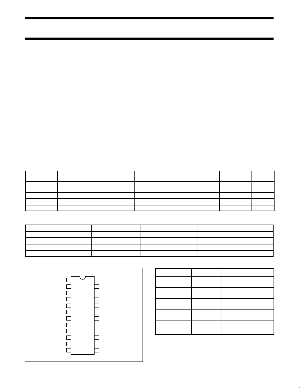
PIN CONFIGURA TION
1
OE
2
D0
3
D1
4
D2
5
D3
6
D4
7
D5
8
D6
9
D7 Q7
10 15
D8
11 14D9
12 13GND
TOP VIEW
24
V
CC
Q0
23
Q1
22
Q2
21
Q3
20
Q4
19
Q5
18
Q6
17
16
Q8
Q9
CP
SA00223
PIN DESCRIPTION
PIN NUMBER SYMBOL FUNCTION
1 OE
2, 3, 4, 5, 6,
7, 8, 9, 10, 11
23, 22, 21, 20, 19,
18, 17, 16, 15, 14
D0-D9 Data inputs
Q0-Q9 Data outputs
13 CP
10 GND Ground (0V)
20 V
CC
Output enable input
(active-Low)
Clock pulse input (active
rising edge)
Positive supply voltage
1995 Sep 06 853-1616 15703
1
Philips Semiconductors Product specification
10-bit D-type flip-flop; positive-edge trigger
(3-State)
LOGIC SYMBOL
234567891011
D0 D1 D2 D3 D4 D5 D6 D7 D8 D9
13
1CPOE
Q0 Q1 Q2 Q3 Q4 Q5 Q6 Q7 Q8 Q9
23 22 21 20 19 18 17 16 15 14
SA00224
LOGIC SYMBOL (IEEE/IEC)
1
13
223
322
421
520
619
718
817
916
10 15
11 14
EN
C2
2D
74ABT821
1
SA00225
FUNCTION TABLE
INPUTS INTERNAL OUTPUTS OPERATING MODE
OE CP Dn REGISTER Q0 – Q9
L
L
↑
↑
l
h
L
H
L
H
L ↑ X NC NC Hold
H
H
↑
↑
Dn
X
NC
Dn
Z
Z
H = High voltage level
h = High voltage level one set-up time
prior to the Low-to-High clock transition
L = Low voltage level
l = Low voltage level one set-up time
prior to the Low-to-High clock transition
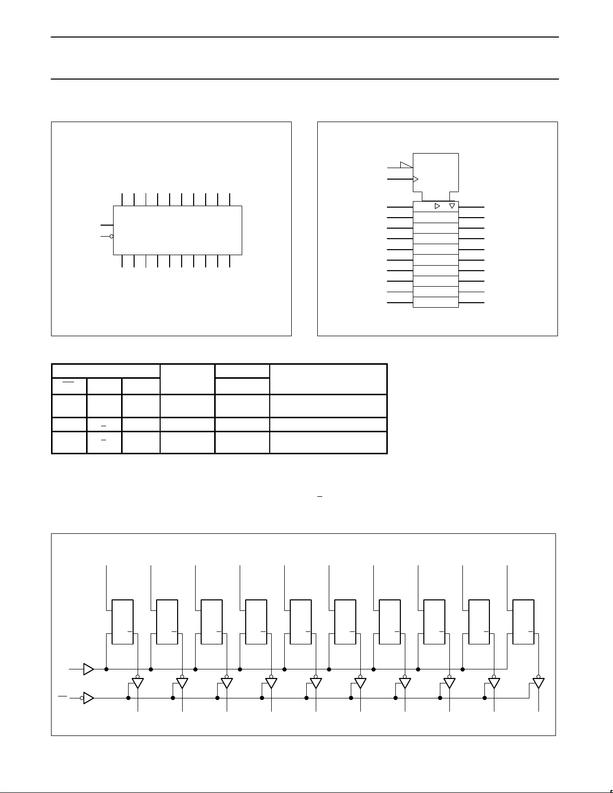
LOGIC DIAGRAM
D0
2
D
CP Q
D1
3
D
CP Q
D2
4
D
CP Q
D3
5
D
CP Q
Load and read register
Disable outputs
NC= No change
X = Don’t care
Z = High impedance “off” state
↑ = Low to High clock transition
= Not a Low-to-High clock transition
↑
D4
6
D
CP Q
D5
7
D
CP Q
D6
8
D
CP Q
D7
9
D
CP Q
D8
10
D
CP Q
D9
11
D
CP Q
13
CP
1
OE
1995 Sep 06
Q0
23
Q1
22
Q2
21
Q3
20
Q4
19
Q5
18
Q6
17
Q7
16
Q8
15
14
Q9
SA00226
2
 Loading...