

Philips 74ABT74N, 74ABT74DB, 74ABT74D Datasheet
Philips Semiconductors Product specification
CC
74ABT74Dual D-type flip-flop
QUICK REFERENCE DAT A
CONDITIONS
= 25°C;
SYMBOL PARAMETER
T
amb
GND = 0V
TYPICAL UNIT
Propagation
IN
CC
delay
CPn to
n
Qn, Q
Output to
Output skew
Input
capacitance
Total supply
current
CL = 50pF;
= 5V
V
CC
VI = 0V or V
CC
Outputs disabled;
= 5.5V
V
CC
3.0
2.5
0.5 ns
3 pF
50 µA
t
PLH
t
PHL
t
OSLH
t
OSHL
C
I
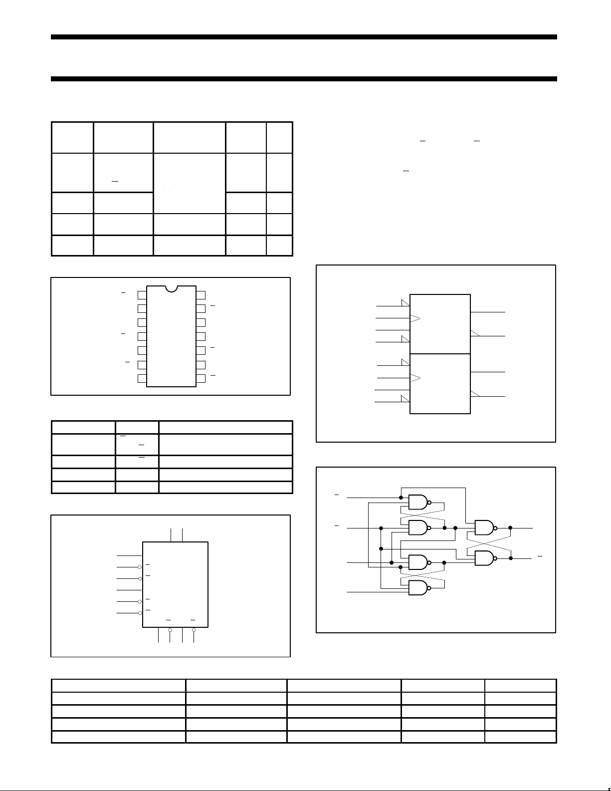
PIN CONFIGURA TION
R
CP0
S
GND
D1
D0
D1
Q0
Q
1
2
3
4
5
6
0
14
V
CC
13
D1
R
12
D1
11
CP1
10
SD1
9
Q1
87
Q1
PIN DESCRIPTION
PIN NUMBER SYMBOL NAME AND FUNCTION
1, 2, 3, 4, 10,
11, 12, 13
RDn, Dn,
CPn, S
Dn
Data inputs
5, 6, 8, 9 Qn, Qn Data outputs
7 GND Ground (0V)
14 V
Positive supply voltage
CC
LOGIC SYMBOL
212
ns
SF00045
DESCRIPTION
The 74ABT74 is a dual positive edge-triggered D-type flip-flop
featuring individual data, clock, set, and reset inputs; also true and
complementary outputs. Set (S
D) and reset (RD) are asynchronous
active low inputs and operate independently of the clock input.
When set and reset are inactive (high), data at the D input is
transferred to the Q and Q
outputs on the low-to-high transition of
the clock. Data must be stable just one setup time prior to the
low-to-high transition of the clock for predictable operation. Clock
triggering occurs at a voltage level and is not directly related to the
transition time of the positive-going pulse. Following the hold time
interval, data at the D input may be changed without affecting the
levels of the output.
LOGIC SYMBOL (IEEE/IEC)
4
3
2
1
10
11
12
13
&
S
C1
1D
R
S
C2
2D
R
5
6
9
8
SF00047
LOGIC DIAGRAM
4, 10
S
D
1, 13
D
R
5, 9
Q
VCC = Pin 14
GND = Pin 7
3
4
1
11
10
13
D0 D1
CP0
S
D0
RD0
CP1
D1
S
D1
R
Q0 Q0Q1Q1
56 98
SA00359
CP
D
VCC = Pin 14
GND = Pin 7
3, 11
2, 12
6, 8
ORDERING INFORMATION
PACKAGES TEMPERATURE RANGE OUTSIDE NORTH AMERICA NORTH AMERICA DWG NUMBER
14-Pin Plastic DIP –40°C to +85°C 74ABT74 N 74ABT74 N SOT27-1
14-Pin plastic SO –40°C to +85°C 74ABT74 D 74ABT74 D SOT108-1
14-Pin Plastic SSOP Type II –40°C to +85°C 74ABT74 DB 74ABT74 DB SOT337-1
14-Pin Plastic TSSOP Type I –40°C to +85°C 74ABT74 PW 74ABT74PW DH SOT402-1
1
853-1813 157931995 Sep 22
Q
SF00048
Philips Semiconductors Product specification
OPERATING
SYMBOL
PARAMETER
UNIT
74ABT74Dual D-type flip-flop
FUNCTION TABLE
INPUTS OUTPUTS
SD RD CP D Q Q
OPERATING
MODE
L H X X H L Asynchronous set
H L X X L H
Asynchronous
reset
L L X X H H Undetermined*
H H ↑ h H L Load “1”
H H ↑ l L H Load “0”
H H ↑ X NC NC Hold
NOTES:
H = High voltage level
h = High voltage level one setup time prior to low-to-high
clock transition
L = Low voltage level
l = Low voltage level one setup time prior to low-to-high
clock transition
NC= No change from the previous setup
X = Don’t care
↑ = Low-to-high clock transition
= Not low-to-high clock transition
↑
* = This setup is unstable and will change when either set
or reset return to the high level.
ABSOLUTE MAXIMUM RATINGS
SYMBOL
V
CC
I
IK
V
I
I
OK
V
OUT
I
OUT
T
stg
DC supply voltage –0.5 to +7.0 V
DC input diode current VI < 0 –18 mA
DC input voltage
DC output diode current VO < 0 –50 mA
DC output voltage
DC output current output in Low state 40 mA
Storage temperature range –65 to 150 °C
PARAMETER CONDITIONS RATING UNIT
3
3
1, 2
–1.2 to +7.0 V
output in Off or High state –0.5 to +5.5 V
NOTES:
1. Stresses beyond those listed may cause permanent damage to the device. These are stress ratings only and functional operation of the
device at these or any other conditions beyond those indicated under “recommended operating conditions” is not implied. Exposure to
absolute-maximum-rated conditions for extended periods may affect device reliability .
2. The performance capability of a high-performance integrated circuit in conjunction with its thermal environment can create junction
temperatures which are detrimental to reliability. The maximum junction temperature of this integrated circuit should not exceed 150°C.
3. The input and output voltage ratings may be exceeded if the input and output current ratings are observed.
RECOMMENDED OPERATING CONDITIONS
LIMITS
MIN MAX
V
CC
V
V
V
I
OH
I
OL
∆t/∆v Input transition rise or fall rate 0 10 ns/V
T
amb
DC supply voltage 4.5 5.5 V
Input voltage 0 V
I
High-level input voltage 2.0 V
IH
Low-level input voltage 0.8 V
IL
High-level output current –15 mA
Low-level output current 20 mA
Operating free-air temperature range –40 +85 °C
CC
V
1995 Sep 22
2
 Loading...