

Philips 74ABT657PW, 74ABT657N, 74ABT657DB, 74ABT657D Datasheet

INTEGRATED CIRCUITS
74ABT657
Octal transceiver with parity
generator/checker (3-State)
Product specification 1995 Dec 11
IC23 Data Handbook

Philips Semiconductors Product specification
Octal transceiver with parity generator/checker
(3-State)
FEA TURES
•Combinational functions in one package
•Low static and dynamic power dissipation with high speed and
high output drive
•Output capability: +64mA/–32mA
•Power-up 3-State
•Latch-up protection exceeds 500mA per Jedec Std 17
•ESD protection exceeds 2000 V per MIL STD 883 Method 3015
and 200 V per Machine Model
DESCRIPTION
The 74ABT657 high-performance BiCMOS device combines low
static and dynamic power dissipation with high speed and high
output drive.
The 74ABT657 is an octal transceiver featuring non-inverting buffers
with 3-State outputs and an 8-bit parity generator/checker, and is
intended for bus-oriented applications. The buffers have a
guaranteed current sinking capability of 64mA. The
Transmit/Receive (T/R
flow through the bidirectional transceivers. Transmit (active-High)
enables data from A ports to B ports; Receive (active-Low) enables
data from B ports to A ports.
) input determines the direction of the data
The Output Enable (OE
placing them in a high impedance condition when the OE
High. The parity select (ODD/EVEN
of odd or even parity systems. The parity (PARITY) pin is an output
from the generator/checker when transmitting from the port A to B
= High) and an input when receiving from port B to A port (T/R
(T/R
= Low). When transmitting (T/R = High) the parity select
(ODD/EVEN
the number of High bits. The parity (PARITY) output then goes to the
logic state determined by the parity select (ODD/EVEN
by the number of High bits on port A. For example, if the parity
select (ODD/EVEN
High bits on port A is odd, then the parity (PARITY) output will be
High, transmitting even parity. If the number of High bits on port A is
even, then the parity (PARITY) output will be Low, keeping even
parity. When in receive mode (T/R
determine the number of High bits. If parity select (ODD/EVEN
Low (even parity) and the number of Highs on port B is:
(1) odd and the parity (PARITY) input is High, then ERROR
High, signifying no error.
(2) even and the parity (PARITY) input is High, then ERROR
asserted Low, indicating an error.
74ABT657
) input disables both the A and B ports by
input is
) input gives the user the option
) input is set, then the A port data is polled to determine
) setting and
) is set Low (even parity), and the number of
= Low) the B port is polled to
) is
will be
will be
QUICK REFERENCE DATA
SYMBOL PARAMETER
t
PLH
t
PHL
C
C
I
CCZ
IN
I/O
Propagation delay
An to Bn or Bn to An
Input capacitance VI = 0V or V
I/O capacitance
Total supply current Outputs disabled; VCC =5.5V 500 nA
CL = 50pF; VCC = 5V 3.3 ns
Outputs disabled;
= 0V or V
V
O
CONDITIONS
= 25°C; GND = 0V
T
amb
CC
CC
TYPICAL UNIT
4 pF
7 pF
ORDERING INFORMATION
PACKAGES TEMPERATURE RANGE OUTSIDE NORTH AMERICA NORTH AMERICA DWG NUMBER
24-Pin Plastic DIP –40°C to +85°C 74ABT657 N 74ABT657 N SOT222-1
24-Pin plastic SO –40°C to +85°C 74ABT657 D 74ABT657 D SOT137-1
24-Pin Plastic SSOP Type II –40°C to +85°C 74ABT657 DB 74ABT657 DB SOT340-1
24-Pin Plastic TSSOP Type I –40°C to +85°C 74ABT657 PW 74ABT657PW DH SOT355-1
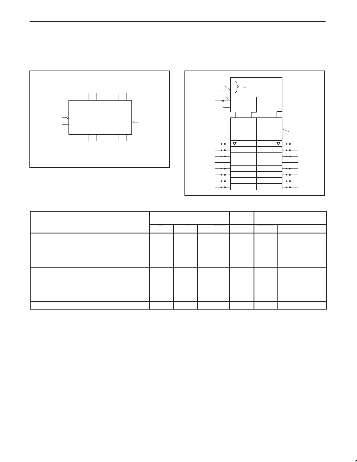
PIN CONFIGURATION
1OE
T/R
2
A0
3
A1
4
A2
5
A3
6
A4
7
V
CC
8
A5
9
A6
10
A7
ODD/EVEN
11
ERROR
TOP VIEW
24
23
22
21
20
19
18
17
16
15
14
1312
B0
B1
B2
B3
GND
GND
B4
B5
B6
B7
PARITY
SA00181
PIN DESCRIPTION
SYMBOL PIN NUMBER NAME AND FUNCTION
13 PARITY Parity output
11 ODD/EVEN Parity select input
12 ERROR Error output
1 T/R Transmit/receive input
2, 3, 4, 5,
6, 8, 9, 10
23, 22, 21, 20,
17, 16, 15, 14
24 OE Output enable input (active-Low)
18, 19 GND Ground (0V)
7 V
A0 - A7 A port 3-State outputs
B0 - B7 B port 3-State outputs
CC
Positive supply voltage
1995 Dec 1 1 853–1615 16106
2
Philips Semiconductors Product specification
Octal transceiver with parity generator/checker
(3-State)
LOGIC SYMBOL
1
24
11
234568910
A0 A1 A2 A3 A4 A5 A6 A7
T/R
OE
ODD/EVEN
B0 B1 B2 B3
23 22 21 20 17 16 15 14
PARITY
ERROR
B4 B5 B6 B7
13
12
SA00182
LOGIC SYMBOL (IEEE/IEC)
74ABT657
1
24
11
223
322
421
520
617
816
915
10 14
0BUSBTOA
0
0
1BUSATOB
M
2
1
2HIGHZ
G3[EVEN]
G4[ODD]
2K =
0
1,3[EVEN]
1,4[ODD]
0,3[EVEN
0,4]ODD
2
13
12
SA00194
FUNCTION TABLE
NUMBER OF HIGH INPUTS
0, 2, 4, 6, 8
1, 3, 5, 7
Don’t care H X X Z Z 3-State
H = High voltage level
L = Low voltage level
X = Don’t care
Z = High impedance ”off” state
INPUTS
INPUT/
OUTPUT
OUTPUTS
OE T/R ODD/EVEN PARITY ERROR OUTPUTS MODE
L
L
L
L
L
L
L
L
L
L
L
L
H
H
L
L
L
L
H
H
L
L
L
L
H
L
H
H
L
L
H
L
H
H
L
L
H
L
H
L
H
L
L
H
H
L
H
L
Z
Z
H
L
L
H
Z
Z
L
H
H
L
Transmit
Transmit
Receive
Receive
Receive
Receive
Transmit
Transmit
Receive
Receive
Receive
Receive
1995 Dec 1 1
3

Philips Semiconductors Product specification
Octal transceiver with parity generator/checker
(3-State)
LOGIC DIAGRAM
1
T/R
24
OE
2
A0
3
A1
4
A2
5
A3
6
A4
8
A5
9
A6
23
22
21
20
17
16
15
74ABT657
B0
B1
B2
B3
B4
B5
B6
ODD/EVEN
10
A7
11
14
B7
13
PARITY
12
ERROR
SA00215
1995 Dec 1 1
4
 Loading...