

Philips 74ABT652AN, 74ABT652ADB, 74ABT652AD Datasheet
Philips Semiconductors Product specification
74ABT652AOctal transceiver/register, non-inverting (3-State)
1
1995 Apr 19 853-1614 15144
FEATURES
•Independent registers for A and B buses
•Multiplexed real-time and stored data
•3-State outputs
•Live insertion/extraction permitted
•Power-up 3-State
•Power-up reset
•Output capability: +64mA/–32mA
•Latch-up protection exceeds 500mA per Jedec JC40.2 Std 17
•ESD protection exceeds 2000 V per MIL STD 883 Method 3015
and 200 V per Machine Model
DESCRIPTION
The 74ABT652A high-performance BiCMOS device combines low
static and dynamic power dissipation with high speed and high
output drive.
The 74ABT652A transceiver/register consists of bus transceiver
circuits with 3-State outputs, D-type flip-flops, and control circuitry
arranged for multiplexed transmission of data directly from the input
bus or the internal registers. Data on the A or B bus will be clocked
into the registers as the appropriate clock pin goes High. Output
Enable (OEAB, OEBA
) and Select (SAB, SBA) pins are provided for
bus management.
QUICK REFERENCE DATA
SYMBOL PARAMETER
CONDITIONS
T
amb
= 25°C; GND = 0V
TYPICAL UNIT
t
PLH
t
PHL
Propagation delay
CPBA to An or CPAB to Bn
CL = 50pF; VCC = 5V
3.7
4.3
ns
C
IN
Input capacitance VI = 0V or V
CC
4 pF
C
I/O
I/O capacitance
Outputs disabled;
V
O
= 0V or V
CC
7 pF
I
CCZ
Total supply current Outputs disabled; VCC =5.5V 110 µA
ORDERING INFORMATION
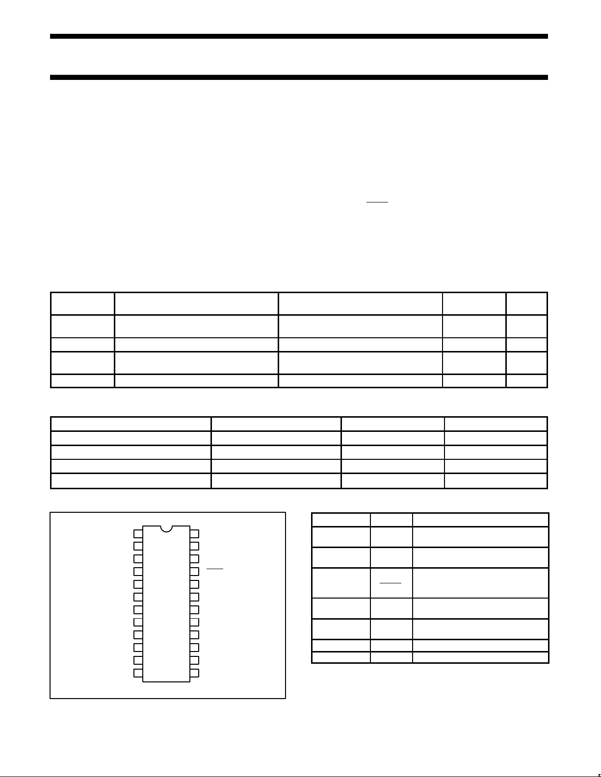
PACKAGES TEMPERATURE RANGE ORDER CODE DRAWING NUMBER
24-pin plastic DIP –40°C to +85°C 74ABT652AN SOT222-1
24-pin plastic SOL –40°C to +85°C 74ABT652AD SOT137-1
24-pin plastic SSOP Type II –40°C to +85°C 74ABT652ADB SOT340-1
24-pin plastic TSSOP Type I –40°C to +85°C 74ABT652APW SOT355-1
PIN CONFIGURATION
SA00094
CPAB
SAB
OEAB
A0
A1
A2
A3
A4
A5
A6
A7
GND
1
2
3
4
5
6
7
8
9
10
11
12
V
CC
CPBA
SBA
OEBA
B0
B1
B2
B3
B4
B5
B6
B713
14
15
16
17
18
19
20
21
22
23
24
PIN DESCRIPTION
PIN NUMBER SYMBOL FUNCTION
1, 23
CPAB /
CPBA
A to B clock input / B to A clock input
2, 22
SAB /
SBA
A to B select input / B to A select
input
3, 21
OEAB /
OEBA
A to B Output Enable input /
B to A Output Enable input
(active–Low)
4, 5, 6, 7,
8, 9, 10, 11
A0 – A7 Data inputs/outputs (A side)
20, 19, 18, 17,
16, 15, 14, 13
B0 – B7 Data inputs/outputs (B side)
12 GND Ground (0V)
24 V
CC
Positive supply voltage
Philips Semiconductors Product specification
74ABT652AOctal transceiver/register, non-inverting (3-State)
1995 Apr 19
2
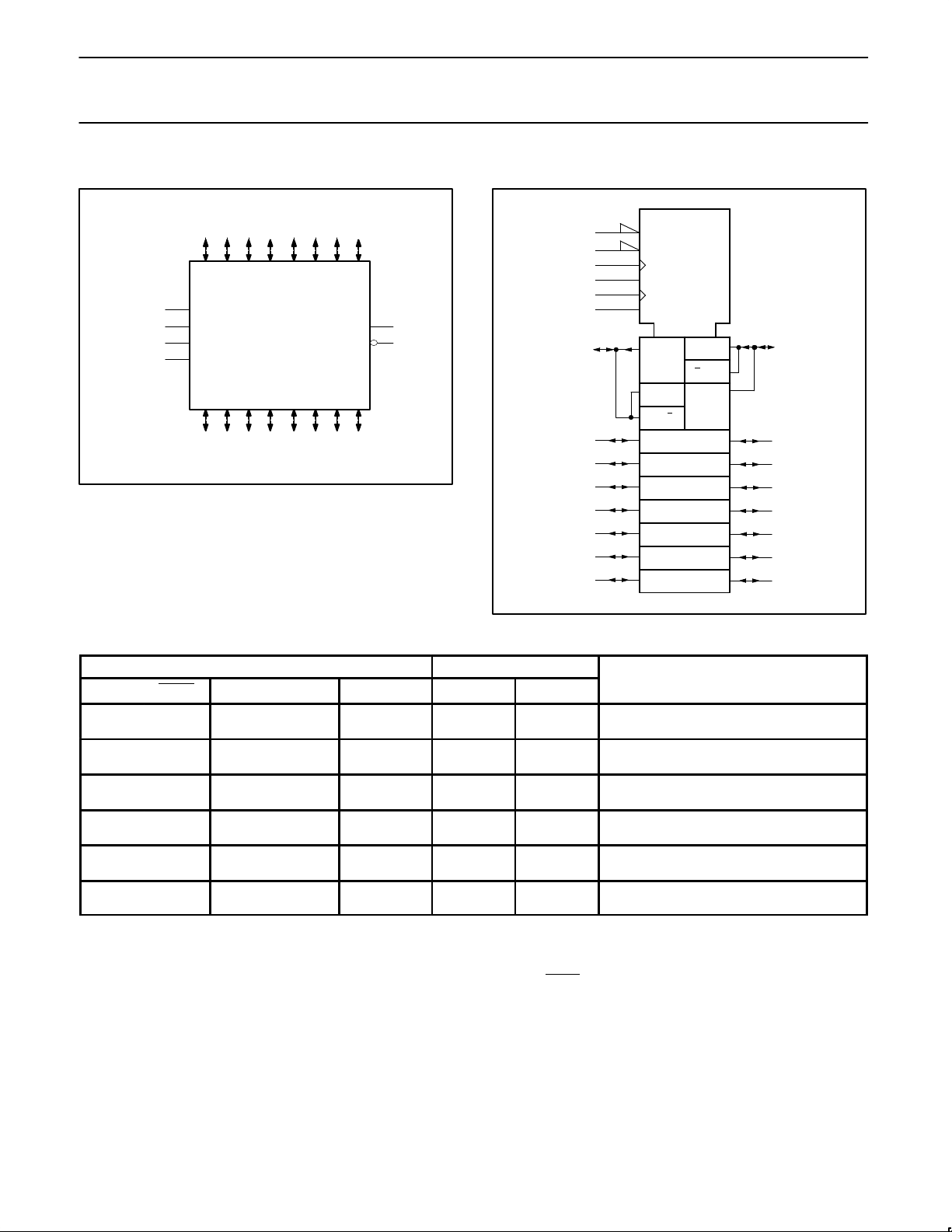
LOGIC SYMBOL
23 CPBA
22 SBA
21OEBA
CPAB1
SAB2
SA00095
B0 B1 B2 B3 B4 B5 B6 B7
20 19 18 17 16 15 14 13
4 5 6 7 8 9 10 11
A0 A1 A2 A3 A4 A5 A6 A7
3OEAB
LOGIC SYMBOL (IEEE/IEC)
SA00096
21
3
23
22
1
2
4
5
6
7
8
9
10
11
EN1 [BA]
EN2 [AB]
C4
G7
C6
G5
20
19
18
17
16
15
14
13
1
1
5 4D
5
1
1
2
6D 7
1 7
FUNCTION TABLE
INPUTS DATA I/O
OEAB OEBA CPAB CPBA SAB SBA An Bn
OPERATING MODE
L
L
H
H
H or L↑H or L
↑
X
X
X
X
Input Input
Isolation
Store A and B data
X
H
H
H
↑
↑
H or L
↑
X
**
X
X
Input
Unspecified
output*
Store A, Hold B
Store A in both registers
L
L
X
L
H or L
↑
↑
↑
X
X
X**Unspecified
output*
Input
Hold A, Store B
Store B in both registers
L
L
L
L
X
X
X
H or L
X
X
L
H
Output Input
Real time B data to A bus
Stored B data to A bus
H
H
H
H
X
H or L
X
X
L
H
X
X
Input Output
Real time A data to B bus
Store A data to B bus
H L H or L H or L H H Output Output
Stored A data to B bus
Stored B data to A bus
H = High voltage level
L = Low voltage level
X = Don’t care
↑ = Low-to-High clock transition
* The data output function may be enabled or disabled by various signals at the OEBA
and OEAB inputs. Data input functions are always
enabled, i.e., data at the bus pins will be stored on every Low-to-High transition of the clock.
** If both Select controls (SAB and SBA) are Low, then clocks can occur simultaneously. If either Select control is High, the clocks must be
staggered in order to load both registers.
Philips Semiconductors Product specification
74ABT652AOctal transceiver/register, non-inverting (3-State)
1995 Apr 19
3
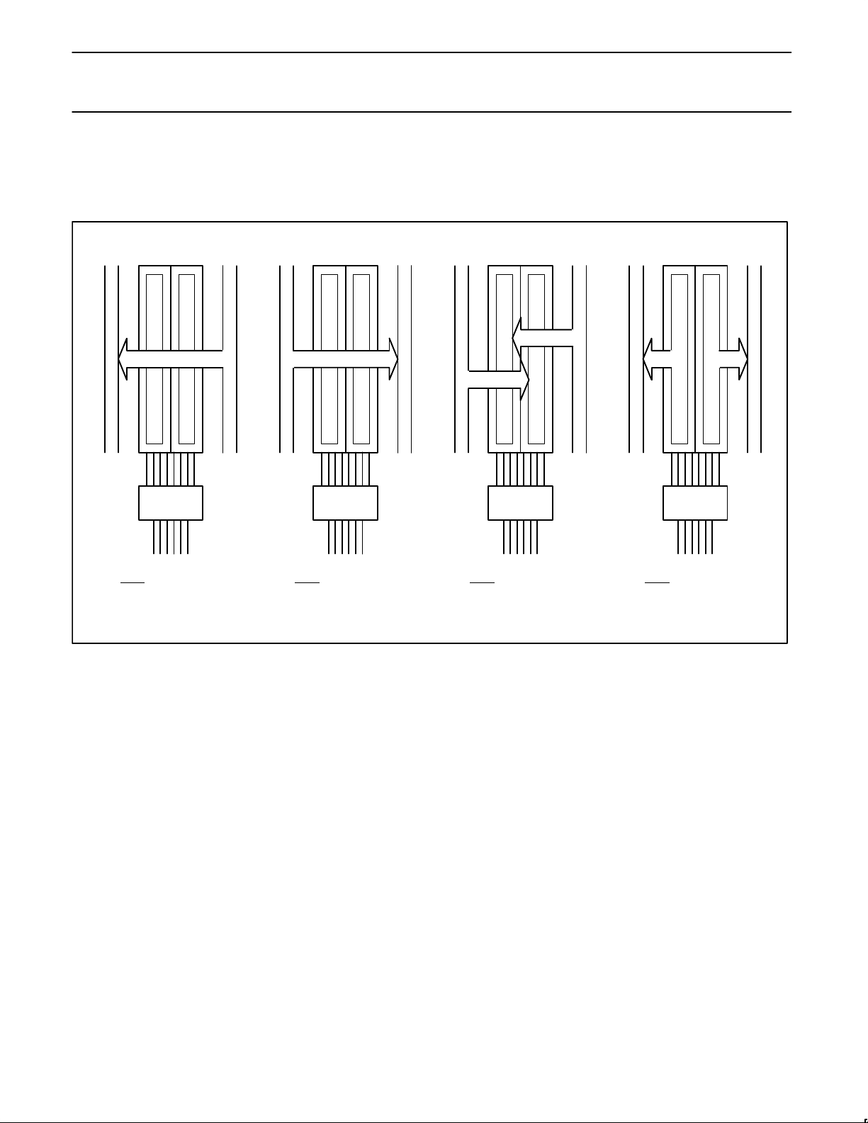
The following examples demonstrate the four fundamental
bus-management functions that can be performed with the
74ABT652A.
The select pins determine whether data is stored or transferred
through the device in real time.
The output enable pins determine the direction of the data flow.
}
REAL TIME BUS TRANSFER
BUS B TO BUS A
OEABOEBA
CPABCPBA SAB SBA
L L X X X L
}
REAL TIME BUS TRANSFER
BUS A TO BUS B
OEABOEBA
CPABCPBA SAB SBA
H H X X L X
}
STORAGE FROM
A, B, OR A AND B
OEABOEBA
CPABCPBA SAB SBA
X H ↑ X X X
L X X ↑ X X
L H ↑ ↑ X X
}
TRANSFER STORED DATA
TO A OR B
OEABOEBA
CPABCPBA SAB SBA
H L H | L H | L H H
SA00097
A B A B A B A B
 Loading...