

Philips 74ABT16245BDL, 74ABT16245BDGG Datasheet

74ABT16245B
74ABTH16245B
16-bit bus transceiver (3-state)
Product specification
Supersedes data of 1996 Nov 20
IC23 Data Handbook
1998 Feb 25
INTEGRATED CIRCUITS
Philips Semiconductors Product specification
74ABT16245B
74ABTH16245B
16-bit bus transceiver (3-State)
2
1998 Feb 25 853-1742 19018
FEA TURES
•16-bit bidirectional bus interface
•Power-up 3-State
•Multiple V
CC
and GND pins minimize switching noise
•3-State buffers
•Output capability: +64 mA/–32mA
•Latch–up protection exceeds 500mA per JEDEC Std 17
•Live insertion/extraction permitted
•ESD protection exceeds 2000 V per MIL STD 883 Method 3015
and 200V per Machine Model
•74ABTH16245B incorporates bus hold data inputs which eliminate
the need for external pull-up resistors to hold unused inputs
•Bus-hold data inputs eliminate the need for external pull-up
resistors to hold unused inputs
DESCRIPTION
The 74ABT16245B high-performance BiCMOS device combines
low static and dynamic power dissipation with high speed and high
output drive.
The 74ABT16245B device is a dual octal transceiver featuring
non-inverting 3-State bus compatible outputs in both send and
receive directions. The control function implementation minimizes
external timing requirements. The device features two Output
Enable (1OE
, 2OE) inputs for easy cascading and two Direction
(1DIR, 2DIR) inputs for direction control.
Two options are available, 74ABT16245B which does not have the
bus hold feature and the 74ABTH16245B which incorporates the
bus hold feature.
QUICK REFERENCE DA TA
SYMBOL PARAMETER
CONDITIONS
T
amb
= 25°C; GND = 0V
TYPICAL UNIT
t
PLH
t
PHL
Propagation delay
nAx to nBx or nBx to nAx
CL = 50pF; VCC = 5V
2.0
2.3
ns
C
IN
Input capacitance VI = 0V or V
CC
4 pF
C
I/O
I/O pin capacitance VO = 0V or VCC; 3-State 7 pF
I
CCZ
pp
Outputs disabled; VCC =5.5V 500 µA
I
CCL
Quiescent su ly current
Output Low; VCC =5.5V 10 mA
ORDERING INFORMATION
PACKAGES TEMPERATURE RANGE OUTSIDE NORTH AMERICA NORTH AMERICA DWG NUMBER
48-Pin Plastic SSOP Type III –40°C to +85°C 74ABT16245B DL BT16245B DL SOT370-1
48-Pin Plastic TSSOP Type II –40°C to +85°C 74ABT16245B DGG BT16245B DGG SOT362-1
48-Pin Plastic SSOP Type III –40°C to +85°C 74ABTH16245B DL BH16245B DL SOT370-1
48-Pin Plastic TSSOP Type II –40°C to +85°C 74ABTH16245B DGG BH16245B DGG SOT362-1
Philips Semiconductors Product specification
74ABT16245B
74ABTH16245B
16-bit bus transceiver (3-State)
1998 Feb 25
3
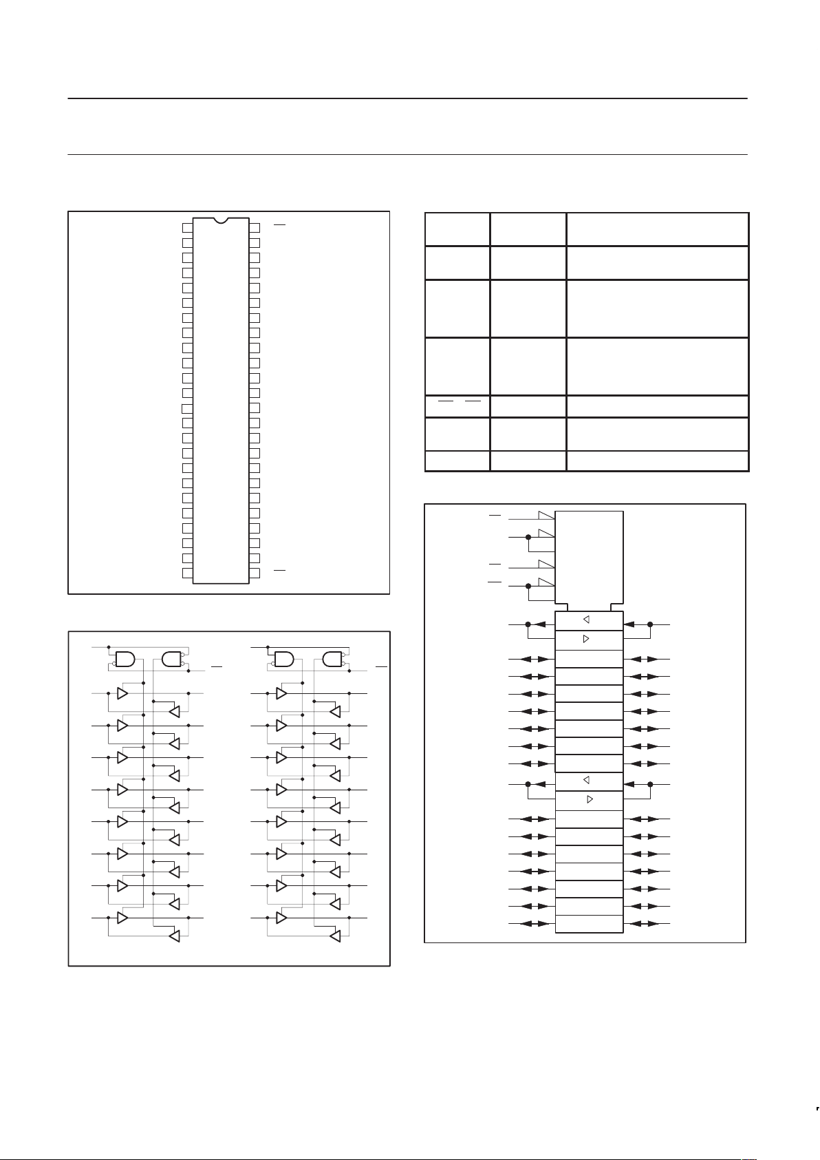
PIN CONFIGURATION
1
2
3
4
5
6
7
8
9
10
11
12
13
14
15
16
17
18
19
20
21
22
23
24
48
47
46
45
44
43
42
41
40
39
38
37
36
35
34
33
32
31
30
29
28
27
26
25
1DIR
1B0
1B1
GND
1B2
1B3
1B4
1B5
GND
1B6
1B7
2B0
2B1
GND
2B3
V
CC
2B4
V
CC
2B2
2B5
GND
2B7
2DIR
2B6
1OE
1A0
1A1
GND
1A2
1A3
1A4
1A5
GND
1A6
1A7
2A0
2A1
GND
2A3
V
CC
2A4
V
CC
2A2
2A5
GND
2A7
2OE
2A6
SA00020
LOGIC SYMBOL
2DIR
24
36
35
33
32
30
29
27
26 23
22
20
19
17
16
14
13
2OE
2A0
2A1
2A2
2A3
2A4
2A5
2A6
2A7
2B0
2B1
2B2
2B3
2B4
2B5
2B6
2B7
25
1DIR
1
47
46
44
43
41
40
38
37 12
11
9
8
6
5
3
2
1OE
1A0
1A1
1A2
1A3
1A4
1A5
1A6
1A7
1B0
1B1
1B2
1B3
1B4
1B5
1B6
1B7
48
SA00021
PIN DESCRIPTION
SYMBOL
PIN
NUMBER
NAME AND FUNCTION
1DIR,
2DIR
1, 24
Direction control inputs
(Active-High)
1A0 – 1A7,
2A0 – 2A7
47, 46, 44, 43
41, 40, 38, 37
36, 35, 33, 32
30, 29, 27, 26
Data inputs/outputs (A side)
1B0 – 1B7
2B0 – 2B7
2, 3, 5, 6
8, 9, 11, 12
13, 14, 16, 17
19, 20, 22, 23
Data inputs/outputs (B side)
1OE, 2OE 48, 25 Output enables
GND
4, 10, 15, 21
28, 34, 39, 45
Ground (0V)
V
CC
7, 18, 31, 42 Positive supply voltage
LOGIC SYMBOL (IEEE/IEC)
∇ 1
48
47
G3
1
3 EN1 (BA)
3 EN2 (AB)
2 ∇
2
3
44 5
43 6
41 8
40 9
38 11
37 12
46
25
24
∇ 4
36
35
5 ∇
13
14
33 16
32 17
30 19
29 20
27 22
26 23
G6
6 EN4 (BA)
6 EN5 (AB)
SA00022
1OE
1DIR
2OE
2DIR
1A0
1A1
1A2
1A3
1A4
1A5
1A6
1A7
2A0
2A1
2A2
2A3
2A4
2A5
2A6
2A7
1B0
1B1
1B2
1B3
1B4
1B5
1B6
1B7
2B0
2B1
2B2
2B3
2B4
2B5
2B6
2B7
Philips Semiconductors Product specification
74ABT16245B
74ABTH16245B
16-bit bus transceiver (3-State)
1998 Feb 25
4
FUNCTION TABLE
INPUTS INPUTS/OUTPUTS
nOE nDIR nAx nBx
L L A = B Inputs
L H Inputs B = A
H X Z Z
H = High voltage level
L = Low voltage level
X = Don’t care
Z = High impedance “off” scale
ABSOLUTE MAXIMUM RATINGS
1, 2
SYMBOL
PARAMETER CONDITIONS RATING UNIT
V
CC
DC supply voltage –0.5 to +7.0 V
I
IK
DC input diode current VI < 0 –18 mA
V
I
DC input voltage
3
–1.2 to +7.0 V
I
OK
DC output diode current VO < 0 –50 mA
V
OUT
DC output voltage
3
output in Off or High state –0.5 to +5.5 V
p
output in Low state 128
I
OUT
DC output current
output in High state –64
mA
T
stg
Storage temperature range –65 to 150 °C
NOTES:
1. Stresses beyond those listed may cause permanent damage to the device. These are stress ratings only and functional operation of the
device at these or any other conditions beyond those indicated under “recommended operating conditions” is not implied. Exposure to
absolute-maximum-rated conditions for extended periods may affect device reliability .
2. The performance capability of a high-performance integrated circuit in conjunction with its thermal environment can create junction
temperatures which are detrimental to reliability. The maximum junction temperature of this integrated circuit should not exceed 150°C.
3. The input and output voltage ratings may be exceeded if the input and output current ratings are observed.
RECOMMENDED OPERATING CONDITIONS
LIMITS
SYMBOL
PARAMETER
Min Max
UNIT
V
CC
DC supply voltage 4.5 5.5 V
V
I
Input voltage 0 V
CC
V
V
IH
High-level input voltage 2.0 V
V
IL
Low-level Input voltage 0.8 V
I
OH
High-level output current –32 mA
I
OL
Low-level output current 64 mA
∆t/∆v Input transition rise or fall rate 0 10 ns/V
T
amb
Operating free-air temperature range –40 +85 °C
 Loading...