

Philips 74ABTH161543DL, 74ABTH161543DGG, 74ABT161543DL, 74ABT161543DGG Datasheet

74ABT161543
74ABTH161543
16-bit latched transceiver with
dual enable and master reset (3-State)
Product specification
Supersedes data of 1995 Sep 18
IC23 Data Handbook
1998 Feb 27
INTEGRATED CIRCUITS
Philips Semiconductors Product specification
74ABT161543
74ABTH161543
16-bit latched transceiver with dual enable
and master reset (3-State)
2
1998 Feb 27 853-1798 19026
FEA TURES
•Two 8-bit octal transceivers with D-type latch
•Live insertion/extraction permitted
•Power-up 3-State
•Power-up reset
•Multiple V
CC
and GND pins minimize switching noise
•Back-to-back registers for storage
•Separate controls for data flow in each direction
•74ABTH161543 incorporates Bus hold data inputs which eliminate
the need for external pull-up resistors to hold unused inputs
•Output capability: +64mA/–32mA
•Latch-up protection exceeds 500mA per Jedec Std 17
•ESD protection exceeds 2000V per MIL STD 883 Method 3015
and 200V per Machine Model
•Same function as ABT16543 except for additional Master Reset
control pins
DESCRIPTION
The 74ABT161543 high-performance BiCMOS device combines low
static and dynamic power dissipation with high speed and high
output drive.
The 74ABT161543 16-bit registered transceiver contains two sets
of D-type latches for temporary storage of data flowing in either
direction. Separate Latch Enable (nLEAB
, nLEBA) and Output
Enable (nOEAB
, nOEBA) inputs are provided for each register to
permit independent control of data transfer in either direction. Master
reset (MR
) clears all registers simultaneously and sets them Low.
The outputs are guaranteed to sink 64mA.
Two options are available, 74ABT161543 which does not have the
Bus hold feature and 74ABTH161543 which inorporates the Bus
hold feature.
QUICK REFERENCE DA TA
SYMBOL PARAMETER
CONDITIONS
T
amb
= 25°C; GND = 0V
TYPICAL UNIT
t
PLH
t
PHL
Propagation delay
nAx to nBx
CL = 50pF; VCC = 5V
2.5
2.2
ns
C
IN
Input capacitance VI = 0V or V
CC
3 pF
C
I/O
I/O capacitance VO = 0V or V
CC;
3-State 7 pF
I
CCZ
pp
Outputs disabled; VCC = 5.5V 500 µA
I
CCL
Quiescent su ly current
Outputs low; V
CC
= 5.5V 9 mA
ORDERING INFORMATION
PACKAGES TEMPERATURE RANGE ORDER CODE DRAWING NUMBER
56-pin plastic SSOP Type III –40°C to +85°C BT161543DL SOT371-1
56-pin plastic TSSOP Type II –40°C to +85°C BT161543DGG SOT364-1
ORDERING INFORMATION
PACKAGES TEMPERATURE RANGE OUTSIDE NORTH AMERICA NORTH AMERICA DWG NUMBER
56-Pin Plastic SSOP Type III –40°C to +85°C 74ABT161543 DL BT161543 DL SOT371-1
56-Pin Plastic TSSOP Type II –40°C to +85°C 74ABT161543 DGG BT161543 DGG SOT364-1
56-Pin Plastic SSOP Type III –40°C to +85°C 74ABTH161543 DL BH161543 DL SOT371-1
56-Pin Plastic TSSOP Type II –40°C to +85°C 74ABTH161543 DGG BH161543 DGG SOT364-1
PIN DESCRIPTION
PIN NUMBER SYMBOL NAME AND FUNCTION
5, 6, 8, 9, 10, 12, 13, 14
15, 16, 17, 19, 20, 21, 23, 24
1A0 – 1A7,
2A0 – 2A7
Data inputs/outputs
52, 51, 49, 48, 47, 45, 44, 43
42, 41, 40,38, 37, 36, 34, 33
1B0 – 1B7,
2B0 – 2B7
Data inputs/outputs
1, 56
28, 29
1OEAB, 1OEBA,
2OEAB, 2OEBA
A to B / B to A Output Enable inputs (active-Low)
3, 54
26, 31
1EAB, 1EBA,
2EAB, 2EBA
A to B / B to A Enable inputs (active-Low)
2, 55
27, 30
1LEAB, 1LEBA,
2LEAB, 2LEBA
A to B / B to A Latch Enable inputs (active-Low)
4, 25 MRab, MRba Master reset
11, 18, 32, 39, 46, 53 GND Ground (0V)
7, 22, 35, 50 V
CC
Positive supply voltage
Philips Semiconductors Product specification
74ABT161543
74ABTH161543
16-bit latched transceiver with dual enable
and master reset (3-State)
1998 Feb 27
3
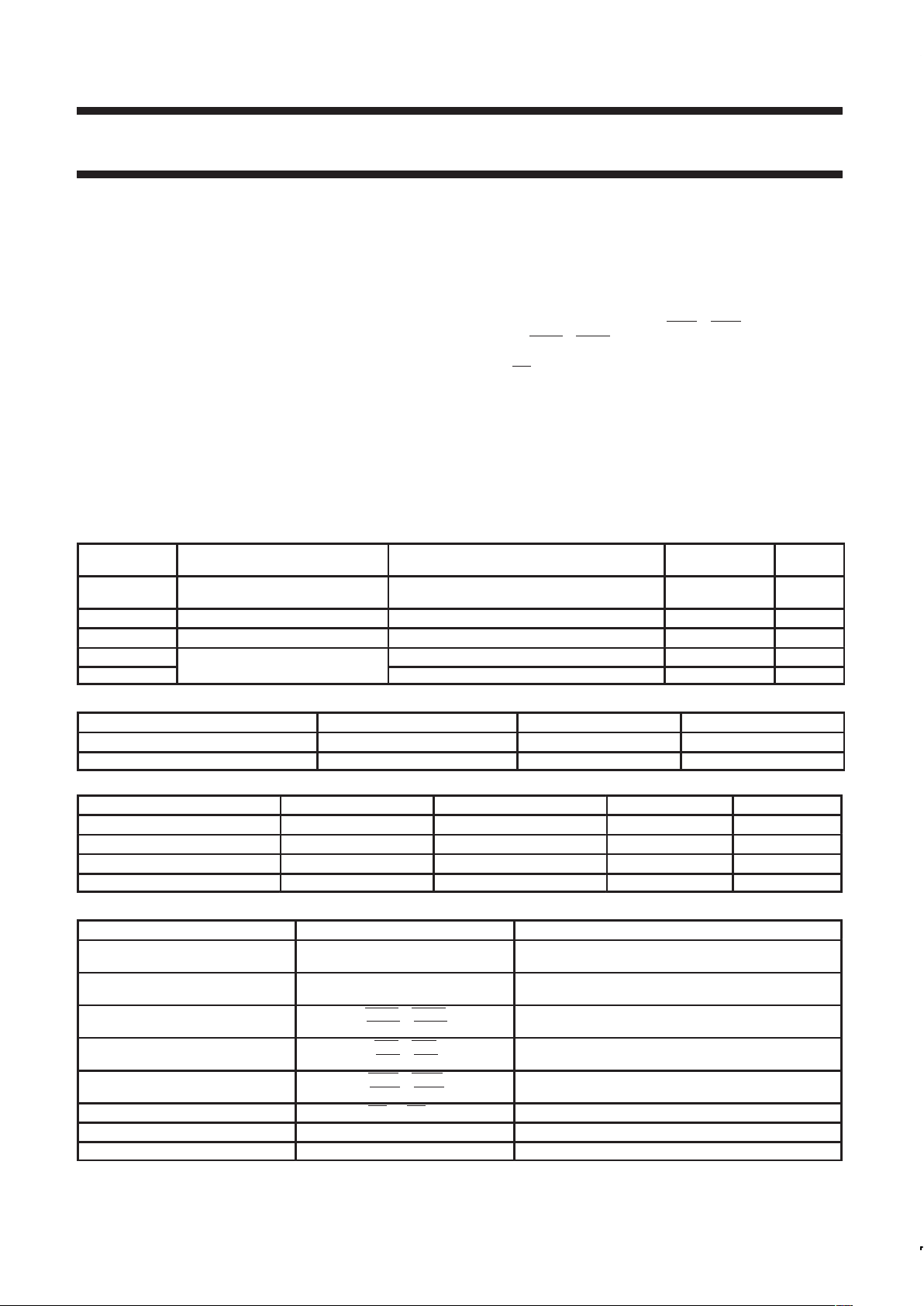
LOGIC SYMBOL (IEEE/IEC)
5
6
8
9
10
12
13
14
16
17
19
20
21
23
24
56
R6/R12
∇3
5D
15
52
51
49
48
47
45
44
43
42
41
40
38
37
36
34
33
6D 4 ∇
∇911D
12D
10 ∇
55
1
3
2
29
31
30
28
26
27
2EN4
G2
2C6
8EN10
G8
8C12
R5/R11
1EN3
G1
1C5
7EN9
SH00060
25
54
4
G7
7C11
MR
ab
1OEAB
1EAB
1LEAB
2OEAB
2EAB
2LEAB
MRba
1OEBA
1EBA
1LEBA
2OEBA
2EBA
2LEBA
1A0
1A1
1A2
1A3
1A4
1A5
1A6
1A7
2A0
2A1
2A2
2A3
2A4
2A5
2A6
2A7
1B0
1B1
1B2
1B3
1B4
1B5
1B6
1B7
2B0
2B1
2B2
2B3
2B4
2B5
2B6
2B7
PIN CONFIGURA TION
1
2
3
4
5
6
7
8
9
10
11
12
13
14
15
16
17
18
19
20
21
22
23
24
25
26
56
55
54
53
52
51
50
49
48
47
46
45
44
43
42
41
40
39
38
37
36
35
34
33
32
31
27
28
30
29
1OEAB
1LEAB
1EAB
MRab
1A0
1A1
1A2
1A3
1A4
GND
1A5
1A6
1A7
2A0
2A2
GND
2A3
V
CC
2A1
2A4
2A5
2A6
2A7
2EAB
V
CC
MRba
2LEAB
2OEAB
1OEBA
1LEBA
1EBA
GND
1B0
1B1
1B2
1B3
1B4
GND
1B5
1B6
1B7
2B0
2B2
GND
2B3
V
CC
2B1
2B4
2B5
2B6
2B7
2EBA
V
CC
GND
2LEBA
2OEBA
SH00061
Philips Semiconductors Product specification
74ABT161543
74ABTH161543
16-bit latched transceiver with dual enable
and master reset (3-State)
1998 Feb 27
4
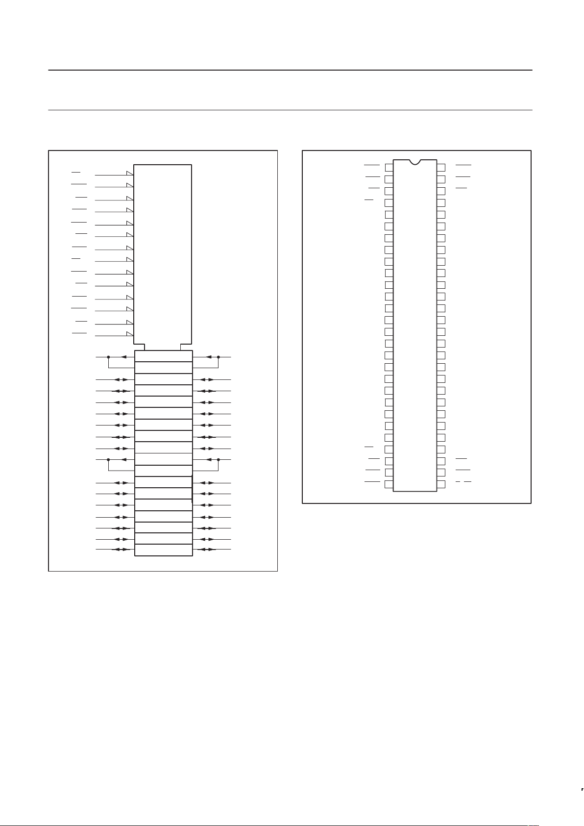
LOGIC SYMBOL
3
54
1EAB
1EBA
2 1LEAB
55 1LEBA
11OEAB
561OEBA
26
31
2EAB
2EBA
27 2LEAB
30 2LEBA
282OEAB
292OEBA
5 6 10 12 13 1489
52 51 47 45 44 4349 48
15 16 20 21 23 2417 19
42 41 37 36 34 3340 38
SH00064
1A0 1A1 1A2 1A3 1A4 1A5 1A6 1A7
1B0 1B1 1B2 1B3 1B4 1B5 1B6 1B7
2A0 2A1 2A2 2A3 2A4 2A5 2A6 2A7
2B0 2B1 2B2 2B3 2B4 2B5 2B6 2B7
4MRab
25MRba
4MRab
25MRba
FUNCTIONAL DESCRIPTION
The 74ABT161543 contains two sets of eight D-type latches, with
separate control pins for each set. Using data flow from A to B as an
example, when the A-to-B Enable (nEAB
) input and the A-to-B Latch
Enable (nLEAB
) input are Low the A-to-B path is transparent.
A subsequent Low-to-High transition of the nLEAB signal puts the A
data into the latches where it is stored and the B outputs no longer
change with the A inputs. With EAB
and nOEAB both Low, the
3-State B output buffers are active and display the data present at
the outputs of the A latches.
Control of data flow from B to A is similar, but using the nEBA
,
nLEBA
, and nOEBA inputs.
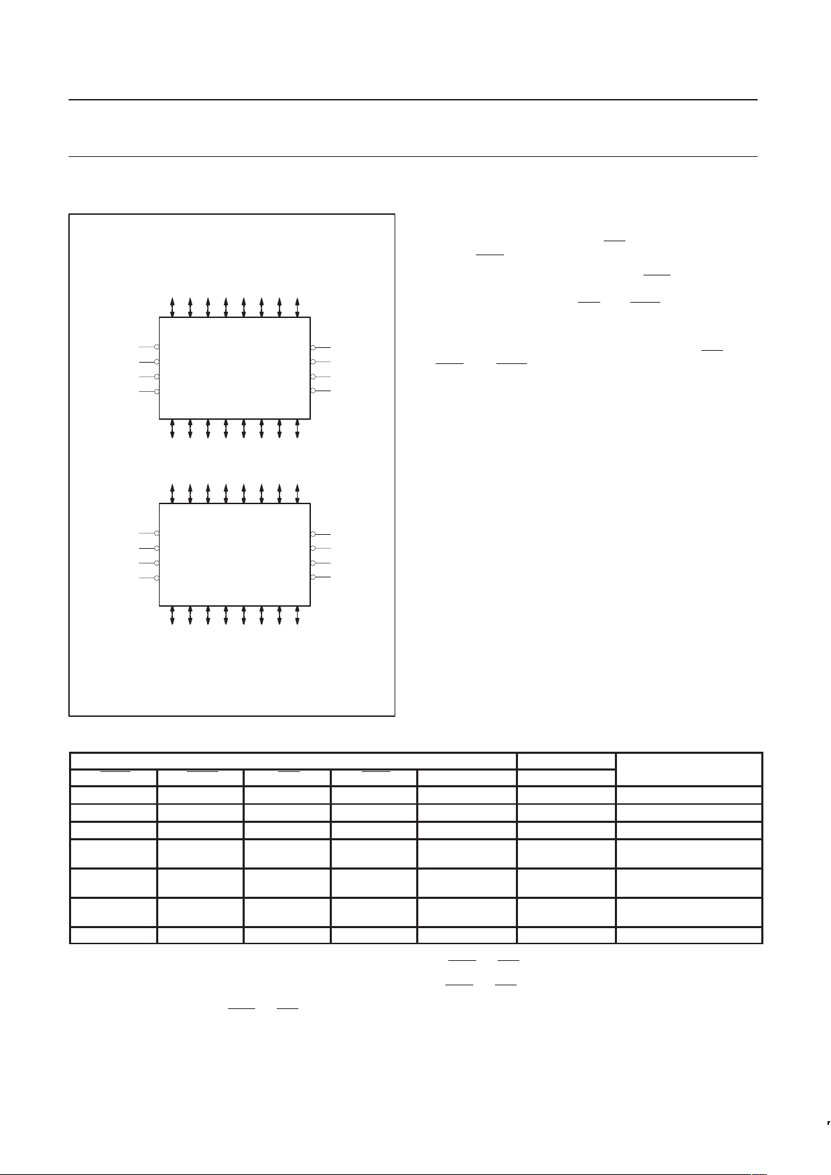
FUNCTION TABLE
INPUTS OUTPUTS
nOEXX nMRXX nEXX nLEXX nAx or nBx nBx or nAx
STATUS
L L L X X L Clear
H X X X X Z Disabled
X X H X X Z Disabled
L
L
H
H
↑
↑
L
L
h
l
Z
Z
Disabled + Latch
L
L
H
H
L
L
↑
↑
h
l
H
L
Latch + Display
L
L
H
H
L
L
L
L
H
L
H
L
Transparent
L H L H X NC Hold
H = High voltage level
h = High voltage level one set-up time prior to the Low-to-High transition of nLEXX
or nEXX (XX = AB or BA)
L = Low voltage level
l = Low voltage level one set-up time prior to the Low-to-High transition of nLEXX
or nEXX (XX = AB or BA)
X = Don’t care
↑ = Low-to-High transition of nLEXX
or nEXX (XX = AB or BA)
NC= No change
Z = High impedance or “off” state
 Loading...