Philips 74abt126 DATASHEETS

INTEGRATED CIRCUITS
74ABT126
Quad buffer (3-State)
Product specification
Supersedes data of 1996 Feb 26
IC23 Data Handbook
1998 Jan 16

Philips Semiconductors Product specification
74ABT126Quad buffer (3-State)
FEA TURES
•Quad bus interface
•3-State buffers
•Live insertion/extraction permitted
•Output capability: +64mA/–32mA
•Latch-up protection exceeds 500mA per JEDEC Std 17
DESCRIPTION
The 74ABT126 high-performance BiCMOS device combines low
static and dynamic power dissipation with high speed and high
output drive.
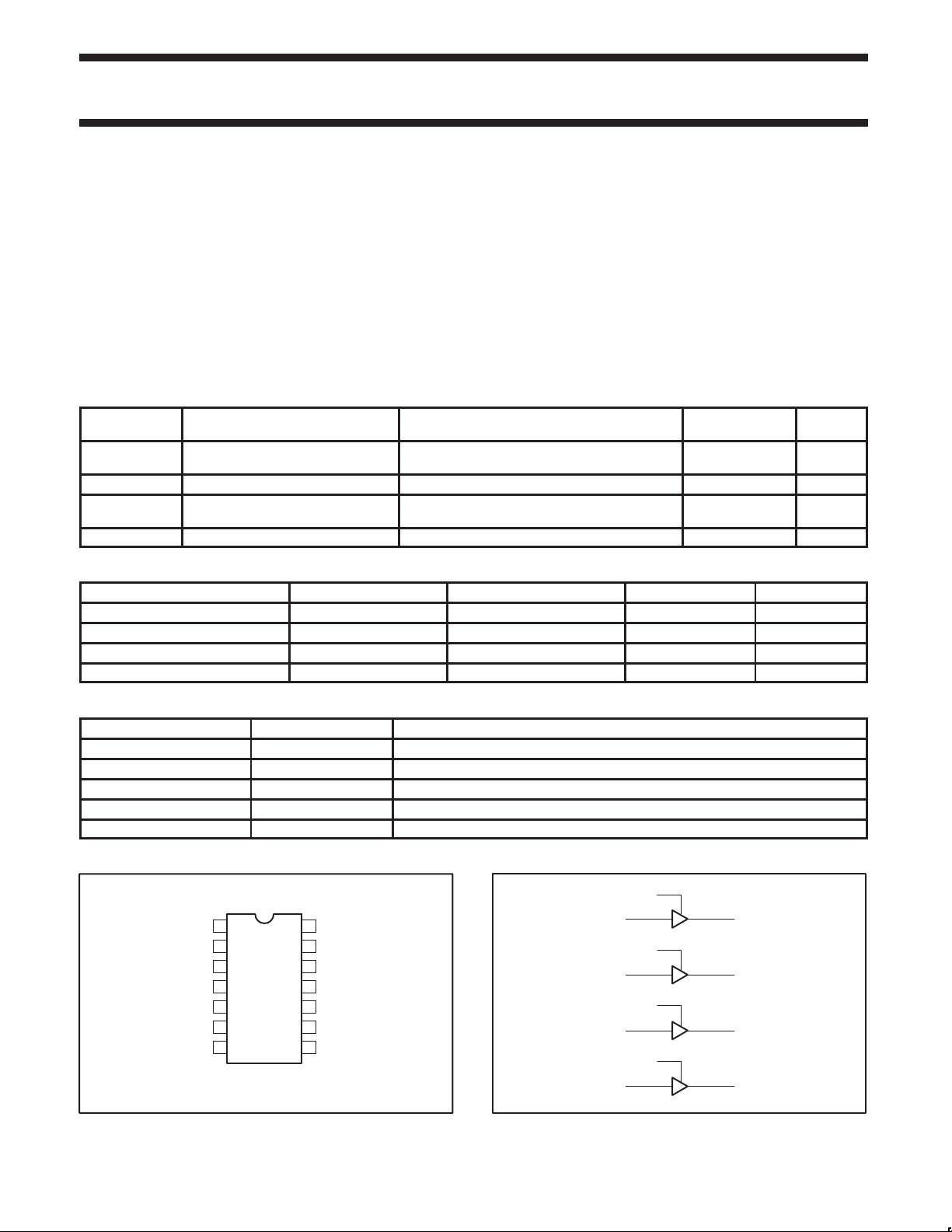
The 74ABT126 device is a quad buffer that is ideal for driving bus
lines. The device features four Output Enables (OE0, OE1, OE2,
OE3), each controlling one of the 3-State outputs.
•ESD protection exceeds 2000V per MIL STD 883 Method 3015
and 200V per Machine Model
•Power-up 3-State
•Inputs are disabled during 3-State mode
QUICK REFERENCE DATA
SYMBOL PARAMETER
C
t
PLH
t
PHL
C
OUT
I
CCZ
IN
Propagation delay
An to Yn
CL = 50pF; VCC = 5V 2.9 ns
Input capacitance VI = 0V or V
Output capacitance
Outputs disabled; VO =
0V or V
CC
Total supply current Outputs disabled; VCC = 5.5V 65 µA
ORDERING INFORMATION
PACKAGES TEMPERATURE RANGE OUTSIDE NORTH AMERICA NORTH AMERICA DWG NUMBER
14-Pin Plastic DIP –40°C to +85°C 74ABT126 N 74ABT126 N SOT27-1
14-Pin plastic SO –40°C to +85°C 74ABT126 D 74ABT126 D SOT108-1
14-Pin Plastic SSOP Type II –40°C to +85°C 74ABT126 DB 74ABT126 DB SOT337-1
14-Pin Plastic TSSOP Type I –40°C to +85°C 74ABT126 PW 74ABT126PW DH SOT402-1
CONDITIONS
T
= 25°C; GND = 0V
amb
CC
TYPICAL UNIT
4 pF
7 pF
PIN DESCRIPTION
PIN NUMBER SYMBOL NAME AND FUNCTION
2, 5, 9, 12 A0 – A3 Data inputs
3, 6, 8, 11 Y0 – Y3 Data outputs
1, 4, 10, 13 OE0 – OE3 Output enable inputs
7 GND Ground (0V)
14 V
PIN CONFIGURATION
OE0
1
A0
2
Y0
3
OE1
4
A1
5
Y1
6
GND Y2
78
CC
14
V
OE3
13
A3
12
Y3
11
OE2
10
A2
9
SA00031
CC
Positive supply voltage
LOGIC SYMBOL
1
OE0
2
A0
4
OE1
5
A1
10
OE2
9
A2
13
OE3
12
A3
3
6
8
11
SA00032
Y0
Y1
Y2
Y3
1998 Jan 16 853–1607 18867
2

Philips Semiconductors Product specification
SYMBOL
PARAMETER
UNIT
74ABT126Quad buffer (3-State)
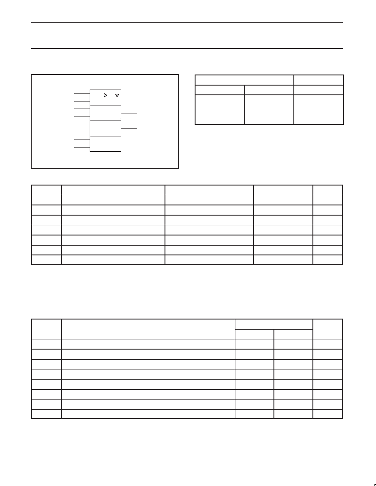
LOGIC SYMBOL (IEEE/IEC)
FUNCTION TABLE
INPUTS OUTPUTS
1
EN
2
4
5
10
9
13
12
1
ABSOLUTE MAXIMUM RATINGS1,
SYMBOL
V
CC
I
IK
V
I
OK
V
OUT
I
OUT
T
stg
NOTES:
1. Stresses beyond those listed may cause permanent damage to the device. These are stress ratings only and functional operation of the
DC supply voltage –0.5 to +7.0 V
DC input diode current VI < 0 –18 mA
DC input voltage
I
DC output diode current VO < 0 –50 mA
DC output voltage
DC output current output in Low state 128 mA
Storage temperature range –65 to 150 °C
PARAMETER CONDITIONS RATING UNIT
3
3
3
6
8
11
SA00461
2
H =High voltage level
L =Low voltage level
X = Don’t care
Z =High impedance ”off” state
output in Off or High state –0.5 to +5.5 V
OEn An Yn
H L L
H H H
L X Z
–1.2 to +7.0 V
device at these or any other conditions beyond those indicated under “recommended operating conditions” is not implied. Exposure to
absolute-maximum-rated conditions for extended periods may affect device reliability .
2. The performance capability of a high-performance integrated circuit in conjunction with its thermal environment can create junction
temperatures which are detrimental to reliability. The maximum junction temperature of this integrated circuit should not exceed 150°C.
3. The input and output voltage ratings may be exceeded if the input and output current ratings are observed.
RECOMMENDED OPERATING CONDITIONS
LIMITS
Min Max
V
CC
V
V
V
I
OH
I
OL
∆t/∆v Input transition rise or fall rate 0 10 ns/V
T
amb
1998 Jan 16
DC supply voltage 4.5 5.5 V
Input voltage 0 V
I
High-level input voltage 2.0 V
IH
Low-level Input voltage 0.8 V
IL
High-level output current –32 mA
Low-level output current 64 mA
Operating free-air temperature range –40 +85 °C
3
CC
V
 Loading...