

Philips 74ABT02PW, 74ABT02N, 74ABT02DB, 74ABT02D Datasheet
INTEGRATED CIRCUITS
74ABT02
Quad 2-input NOR gate
Product specification 1995 Sep 18
IC24 Data Handbook
Philips Semiconductors Product specification
CC
74ABT02Quad 2-input NOR gate
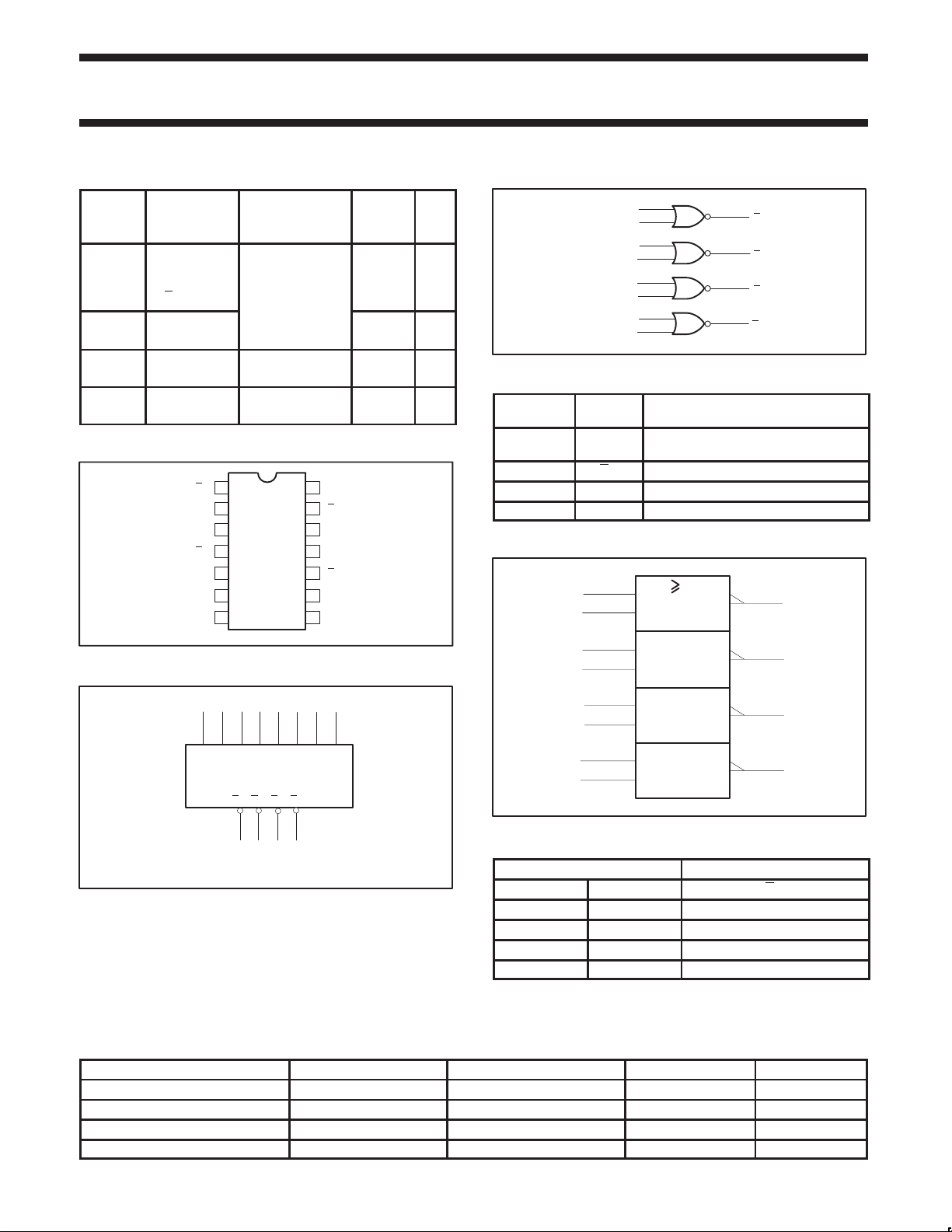
QUICK REFERENCE DATA
CONDITIONS
SYMBOL PARAMETER
T
Propagation
IN
CC
delay
An or Bn
to Yn
Output to
Output skew
Input
capacitance
Total supply
current
CL = 50pF;
V
VI = 0V or V
Outputs disabled;
VCC = 5.5V
t
PLH
t
PHL
t
OSLH
t
OSHL
C
I
PIN CONFIGURATION
Y
1
0
A0
2
B0
3
1
Y
4
A1
5
B1
6
GND
LOGIC SYMBOL
2356891112
= 25°C;
amb
GND = 0V
= 5V
SA00337
LOGIC DIAGRAM
2
A0
3
B0
5
A1
6
B1
8
A2
9
B2
11
A3
12
B3
SYMBOL NAME AND FUNCTION
An-Bn Data inputs
CC
TYPICAL UNIT
2.4
1.8
ns
0.4 ns
3 pF
50 µA
= Pin 14
V
CC
GND = Pin 7
PIN DESCRIPTION
PIN
NUMBER
2, 3, 5, 6, 8,
9, 11, 12
1, 4, 10, 13 Yn Data outputs
14
V
CC
Y
3
13
B3
12
A3
11
Y2
10
B2
9
A2
87
7 GND Ground (0V)
14 V
Positive supply voltage
CC
LOGIC SYMBOL (IEEE/IEC)
2
3
5
6
8
9
1
0
Y
4
1
Y
10
Y2
13
Y
3
SA00335
1
1
4
10
VCC = Pin 14
GND = Pin 7
Y0Y1Y2Y3
1 4 10 13
B2A2A0 B0 B1A1 A3 B3
SA00362
FUNCTION TABLE
An Bn Yn
11
12
13
SF00010
INPUTS OUTPUT
L L H
L H L
H L L
H H L
NOTES:
H = High voltage level
L = Low voltage level
ORDERING INFORMATION
PACKAGES TEMPERATURE RANGE OUTSIDE NORTH AMERICA NORTH AMERICA DWG NUMBER
14-Pin Plastic DIP –40°C to +85°C 74ABT02 N 74ABT02 N SOT27-1
14-Pin plastic SO –40°C to +85°C 74ABT02 D 74ABT02 D SOT108-1
14-Pin Plastic SSOP Type II –40°C to +85°C 74ABT02 DB 74ABT02 DB SOT337-1
14-Pin Plastic TSSOP Type I –40°C to +85°C 74ABT02 PW 74ABT02PW DH SOT402-1
1995 Sep 18 853-1808 15754
2
Philips Semiconductors Product specification
SYMBOL
PARAMETER
UNIT
74ABT02Quad 2-input NOR gate
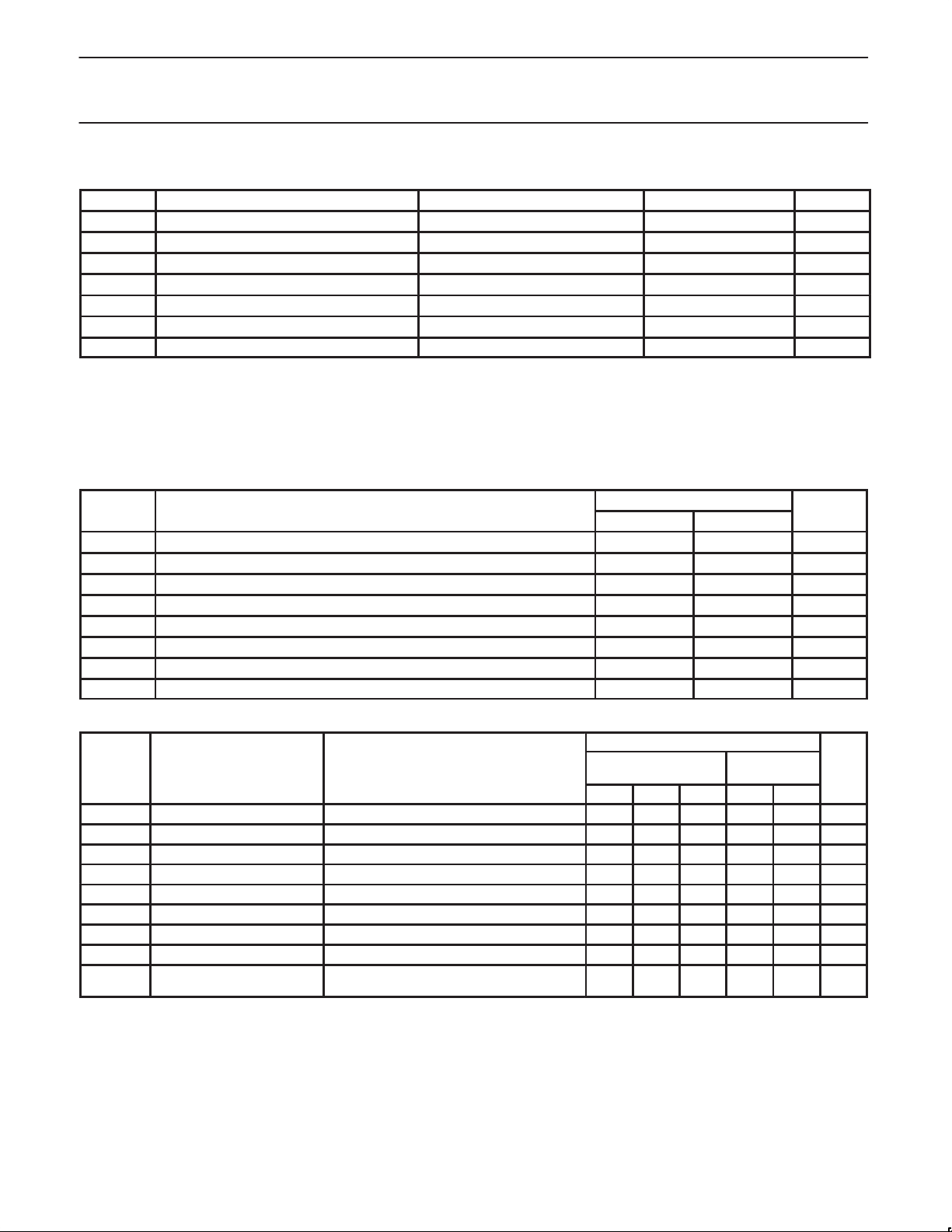
ABSOLUTE MAXIMUM RATINGS
1, 2
SYMBOL PARAMETER CONDITIONS RATING UNIT
V
I
V
I
V
I
OK
OUT
OUT
T
DC supply voltage –0.5 to +7.0 V
CC
DC input diode current VI < 0 –18 mA
IK
I
DC input voltage
3
–1.2 to +7.0 V
DC output diode current VO < 0 –50 mA
DC output voltage
3
output in Off or High state –0.5 to +5.5 V
DC output current output in Low state 40 mA
Storage temperature range –65 to 150 °C
stg
NOTES:
1. Stresses beyond those listed may cause permanent damage to the device. These are stress ratings only and functional operation of the
device at these or any other conditions beyond those indicated under “recommended operating conditions” is not implied. Exposure to
absolute-maximum-rated conditions for extended periods may affect device reliability .
2. The performance capability of a high-performance integrated circuit in conjunction with its thermal environment can create junction
temperatures which are detrimental to reliability. The maximum junction temperature of this integrated circuit should not exceed 150°C.
3. The input and output voltage ratings may be exceeded if the input and output current ratings are observed.
RECOMMENDED OPERATING CONDITIONS
LIMITS
MIN MAX
V
V
V
V
I
OH
I
OL
∆t/∆v Input transition rise or fall rate 0 5 ns/V
T
amb
DC supply voltage 4.5 5.5 V
CC
Input voltage 0 V
I
High-level input voltage 2.0 V
IH
Low-level input voltage 0.8 V
IL
High-level output current –15 mA
Low-level output current 20 mA
Operating free-air temperature range –40 +85 °C
CC
V
DC ELECTRICAL CHARACTERISTICS
LIMITS
SYMBOL PARAMETER TEST CONDITIONS
V
V
V
I
OFF
I
CEX
I
∆I
Input clamp voltage VCC = 4.5V; IIK = –18mA –0.9 –1.2 –1.2 V
IK
High-level output voltage VCC = 4.5V; IOH = –15mA; VI = VIL or V
OH
Low-level output voltage VCC = 4.5V; IOL = 20mA; VI = VIL or V
OL
I
Input leakage current VCC = 5.5V; VI = GND or 5.5V ±0.01 ±1.0 ±1.0 µA
I
IH
IH
Power-off leakage current VCC = 0.0V; VO or VI ≤ 4.5V ±5.0 ±100 ±100 µA
Output High leakage current VCC = 5.5V; VO = 5.5V; VI = GND or V
I
Output current
O
Quiescent supply current VCC = 5.5V; VI = GND or V
CC
Additional supply current per
CC
input pin
1
2
VCC = 5.5V; VO = 2.5V –50 –75 –180 –50 –180 mA
VCC = 5.5V; One data input at 3.4V, other
inputs at V
or GND
CC
CC
CC
NOTES:
1. Not more than one output should be tested at a time, and the duration of the test should not exceed one second.
2. This is the increase in supply current for each input at 3.4V.
T
= +25°C
amb
MIN TYP MAX MIN MAX
2.5 2.9 2.5 V
0.35 0.5 0.5 V
5.0 50 50 µA
2 50 50 µA
0.25 500 500 µA
T
amb
to +85°C
= –40°C
UNIT
1995 Sep 18
3
 Loading...