Philips 5-DTC-Module-MP-3 Service Manual
10-1 10-1
TABLE OF CONTENTS
Service hints ...............................................................................10-1
Location of Printed Circuit Boards..............................................10-3
Wiring ..........................................................................................10-3
Emergency opening....................................................................10-4
Location of switches....................................................................10-4
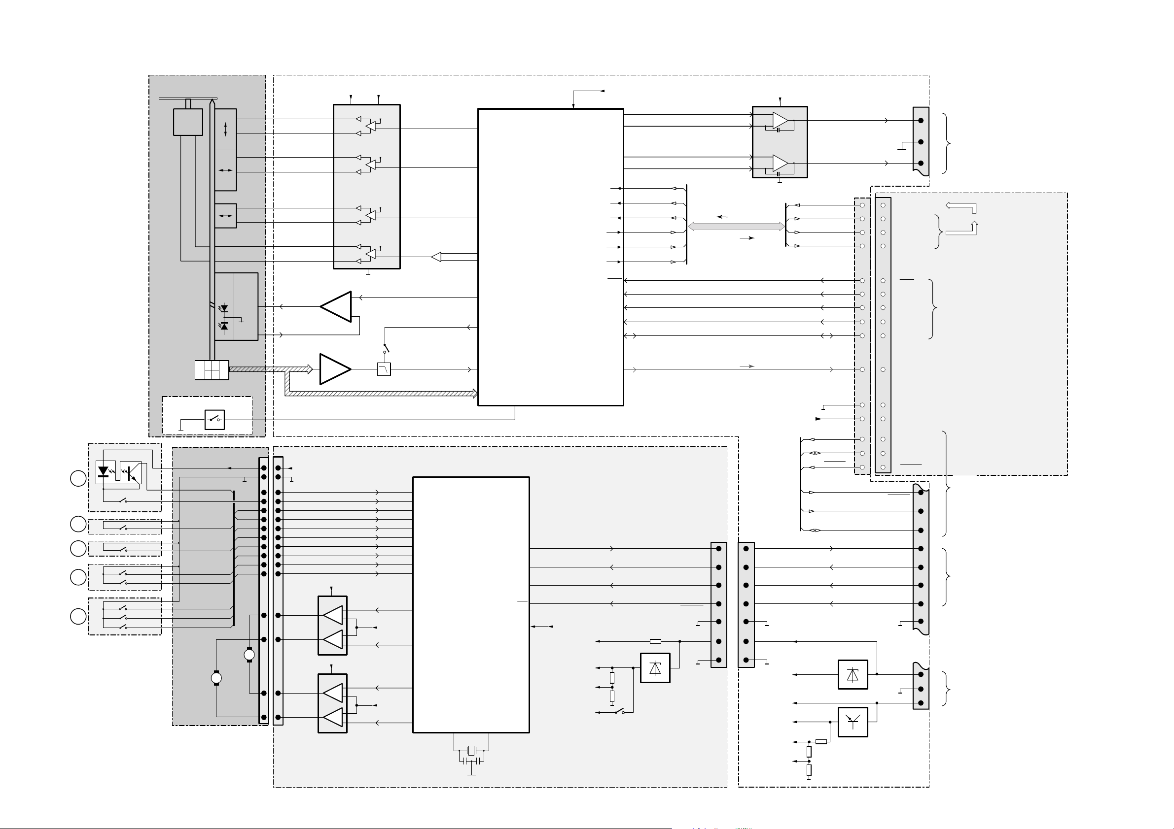
Blockdiagram..............................................................................10-5
CD BOARD
Circuit Diagram .......................................................................10-6
Component Layout side A.......................................................10-7
Component Layout side B.......................................................10-8
CONTROL BOARD
Circuit Diagram .......................................................................10-9
Component Layout .................................................................10-9
MP3 BOARD (for orientation only)
Circuit Diagram .....................................................................10-10
Component Layout ...............................................................10-11
Exploded view loader ...............................................................10-12
Partslist.....................................................................................10-13
5DTC Module
(MP3 version)
Layout stage CD .5/ Control .4
In case of symptom „skipping tracks“ perform following actions:
1. VERIFY THE COMPLAINT
PLAYABILITY CHECK
Use CDDA SBC 444A: . . . . . . . . . . . . .4822 397 30245
TR 14 (600µ black dot) maximum at 01:15
TR 19 (fingerprint)
TR 10 (1000µ wedge)
Use CD-RW Printed Audio Disk . . . . . .7104 099 96611
TR 3 (Fingerprint)
TR 8 (600µ black dot) maximum at 01:00
• playback of all these tracks without audible disturbance
• jump forward/backward within a reasonable time
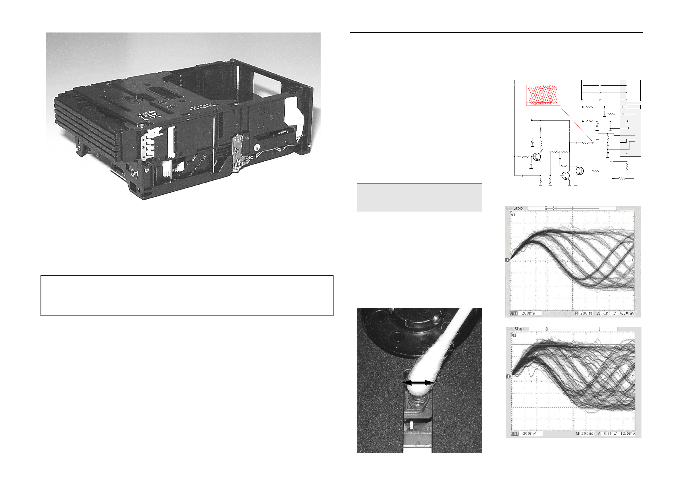
2. CLEAN THE LENS
CD DRIVE – LENS CLEANING
Because the material of the lens is synthetic and coated
with a special anti-reflectivity layer, cleaning must be
done with a non-aggressive cleaning fluid.It is advised to
use “KODAK LENS CLEANER CAT 176 71 36”, available
in normal photo shops.
The actuator is a very precise mechanical component
and may not be damaged in order to guarantee its full
function. It is advised to clean the lens gently (don’t press
too hard) with a soft and clean cotton bud moistened with
the special lens cleaner.
The direction of cleaning must be in the way as indicated
in the picture below.
3. MEASURE THE EYE-PATTERN SIGNAL
EYE-PATTERN SIGNAL – JITTER MEASUREMENT
Measure the signal direct on resistor 3898 using an oscilloscope (see also chapter 10-9).
See below examples of the signal.Amplitude should read at
least 700mVpp using SBC444A.
good
bad
If the oscilloscope shows a signal like the ‘bad’ one, and/or
the amplitude decreases within 1minute - the CD drive has
to be replaced.
Sanyo
DA12T3
HF-Amplifier
D3
D2
D1
Drive detection
680R
3905
3903
3K3
BC847B
7877
47n
2818
1K5
3902
5
7
4
2
1
6
3
64
8
9
10
11
470R
3893
+3.3V
2K2
3908
10K
3923
BC847B
7878
BC847B
7876
4n7
2813
3896
100R
220u
2885
2881
560p
47n
2887
560R
3901
2883
470n
2817
4u7
3n3
2814
3898
220R
3895
27K
470n
2884
+3.3V
3909
820R
3907
100R
3920
33K
3897
2882
82p
3K3
3904
2K7
3899
3906
470R
+5V_HF
HFIN
VrefCD10
100p
28152816
22n
LDON
to 3826,3827
VREF GEN.
VDDA1
VRIN
VSSA1
ISLICE
LDON
D1
D2
D3
D4
HFIN
HFREF
IREF
CD_DA: 0V / CD_RW: 3V
Σ (A-D)
800mVpp
TB = 0.5µs/div
EYE-PATTERN
1,8V
1,2V
2,4V
2,6V
0,65V
Before touching the lens it is advised to clean
the surface of the lens by blowing clean air over
it in order to avoid that little particles make
scratches on the lens.
Service Hints
10-2 10-2
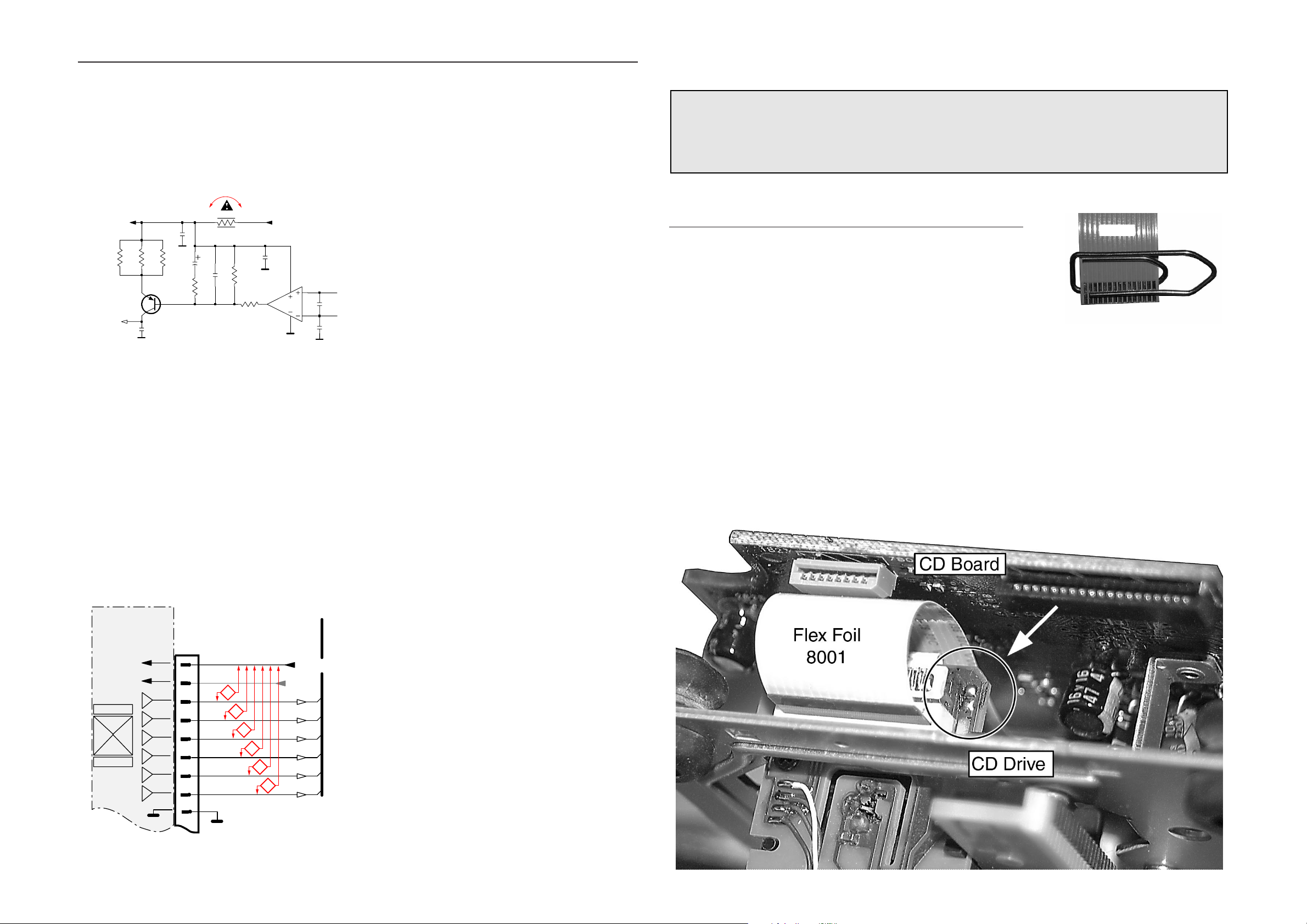
4. MEASURE THE LASER CURRENT
CD DRIVE – LASER CURRENT MEASUREMENT
The laser current can be measured as a voltage drop on
resistor 3820.Typical value 170 - 190mV for CD-DA respectively 200 - 220mV for CD-RW.
5. MEASURE THE OFFSETS OF THE CD-DRIVE
CD DRIVE – OFFSET MEASUREMENT
Each photodiode of the CD-drive may have an offset.
This offset has to be compensated by the signal processor.A high offset of the CD-dr ive leads to poor playability
of some CDs (skipping tracks).
Start the Service Test Program - section „Focus Test“
without a CD.Focus sensitivity = CD-RW.
Use a DC Millivoltmeter for measurement.The offsets
can be measured direct on the connector.See drawing
below.
The values from diode A-D should read
0±10mV. Diodes E and F are less critical.
If one of the offsets is higher than ±10mV the CD drive
has to be replaced.
Sanyo DA12T3
CD Drive
A
A
F
C
B
E
C
D
E
VCC
B
VREF
F
D
9
10
11
12
13
14
15
16
1800
+5V_HF
VrefCD10
A
D
E
B
C
F
GND
8
E
D
A
B
C
F
Laser power control
(example for DA2x drive)
100n
2878
470n
2876
3821
1R
1K
3823
2880
33p
+5V
BC807-40
7879
3817
47R
3820
4R7
47R
3819
1n
2879
2877
47u
1
8
4
7811-A
LM358D
3
2
10K
3822
47R
3818
2841
100n
47n
2869
+5V_HF
LASER DIODE
U >250mV
->Laser damaged !
4,6V
3V
3,3V
3,9V
2V
0,17V
0,17V
Service Hints
The CD drive forms a compact building block with the CD Board.
The following steps have to be done when replacing the CD mechanism:
1. Desolder disc and slide motor
2. Loosen 2x screw
1. Disconnect flexfoil from old CD drive
2. Put a paperclip over contacts of flexfoil to short-circuit the contacts (fig.1)
3. Remove old CD drive
4. Mount new CD drive to CD board
5. Solder disc and slide motor after fixing the drive to the board
5. Move slide outside
6. Remove paperclip from flexfoil
7. Connect flexfoil to new CD drive
8. Remove ESD-protection (solder joint) from laserunit (see picture below)
CHARGED CAPACITORS ON THE SERVO BOARD MAY DAMAGE THE CD DRIVE ELECTRONICS WHEN
CONNECTING A NEW CDM MECHANISM.THAT´S WHY, BESIDES THE SAFETY MEASURES LIKE
• SWITCH OFF POWER SUPPLY
• ESD PROTECTION
ADDITIONAL ACTIONS MUST BE TAKEN BY THE REPAIR TECHNICIAN.
WARNING
fig.1
Attention: The laser diode of this CD dr ive is protected against ESD by a solder joint which shortcircuits the
laserdiode to ground.
For proper functionality of the CD drive this solder joint must be removed after connection the drive to
the set.
10-3 10-3
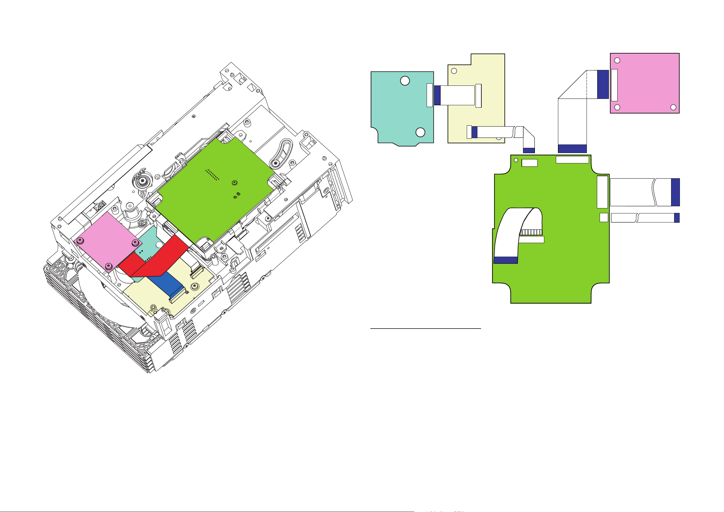
Location of Printed Circuit Boards
5DTC Location of PCBs 2002 08 29
CD Board
Control
Board
Motor
Board
MP3 Board
8051
8052
8021
Wiring Diagram 5DTC Module
5DTC Wiring Diagram 2002 08 30
8001
8052
dig.out (optional)
8051
to / from
AF Board
to / from
CD-drive
1825
1820
1800
1824
1802
1801
1451
1823
Control Board
Motor Board
MP3 Board
CD Board
8021
The FFC-Cables are available as sparepart.
8001 3103 308 93090 FFC CABLE 16Pin 80mm BD Connection from CD Board to CD Drive
8051 3103 308 93100 FFC-CABLE 19Pin 90mm AD Connection from CD Board to MP3 Board
8052 3103 308 93120 FFC CABLE 8Pin 80mm BD Connection from CD Board to Control Board
8021 3103 308 93110 FFC-CABLE 16Pin 60mm AD Connection from Control Board to Motor Board
10-4 10-4
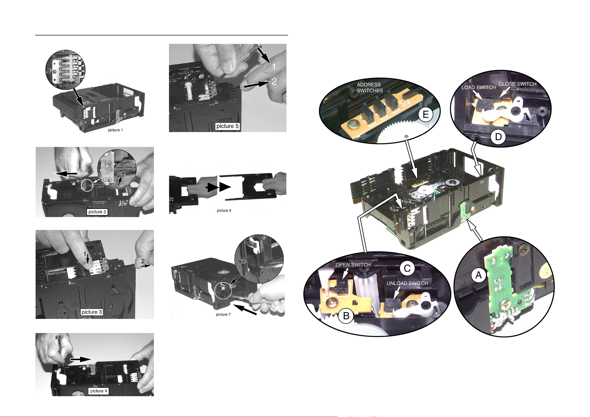
The trays of the 5DTC are mechanically
locked.
To open tray 1, 2 and 3 move lever (pos 29) backwards
(e.g. with a screwdriver - see picture 2) to its endposition.
Release the locking mechanism and pull out the tray (see
picture 3).
To open tray 4 and 5 move lever (pos 29) forward to its
endposition (see picture 4).
Release snap as shown in picture 5 and pull tray out.
To remove a CD from Play Position perform following
steps:
1. Open tray 1 as described before.
2. Tear the tray out with speed (see picture 6).The tray can
be inserted aftewards without any alignment.
3. Move lever (pos 29) forward to its endposition (see picture 4).
4. Push lever (pos 31) forward (see picture 7).
5. Remove CD.
Emergency opening of the trays Location of switches
10-5 10-5
MP3 Version
MP3 Version
1820
15
17
13
16
1824
1824
8
7
10
9
11
CD_IIS_DATA
IIS_WCLK
IIS_SCLK
MP3-Decoder
Communication
Front-µP and MP3 module
RAB
41
RESET
SDA
µP_DATA
12
µP_CLK
11
14
µP_FRAME
SICL
3
2
4
µP_CLK
µP_FRAME
µP_DATA
µP_CLK
µP_FRAME
µP_DATA
SILD
6
SPDIF
Control Logic
Communication
DSP ↔ Signal Processor
WCLI
35
WCLK
28
SCLI
37
SCLK
29
SDI
36
DATA
27
CD_IIS_DATA
AU_IIS_DATA
AU_IIS_DATA
IIS_WCLK
IIS_SCLK
AU_IIS_DATA
IIS_WCLK
IIS_SCLK
1,5,12,14,18
19
CD_IIS_DATA
IIS_SCLK
IIS_WCLK
22
23
RN
RP
DIGITAL AUDIO
MP3 coded
Digital out
CD-DA coded
38
42
40
39
GND
+5V
GND
+5V
For DIGITAL OUT versions only
MP3 BOARD
DOBM
51
10
VCC
7803
7801
TCA0372
TMP87CA409A
V1
D1
D2
D3
D4
R1,R2
Micro Controller
SIGNAL PROCESSOR
CD10
SAA7324 (SAA7325)
TRAY
MOTOR
VDD
DIODES
PHOTO
INNER SWITCH
not on all versions
LASER &
MONITOR
DIODE
TURNTABLE
MOTOR
DISC
CD MECHANISM CD MAINBOARD
CONTROL BOARDMOTOR BOARD
TRAY_IRQ
I2C_SCL
ADDRESS3 SW
ADDRESS3 SW
CLOSE SW
CLOSE SW
ADDRESS2 SW
ADDRESS2 SW
LOAD SW
LOAD SW
ADDRESS1 SW
ADDRESS1 SW
UNLOAD SW
UNLOAD SW
HOLDER HEIGHT COLLECTOR
HOLDER HEIGHT COLLECTOR
OPEN SW
OPEN SW
HOME SW
HOME SW
I2C_SDA
OSC.
DISC SENSOR COLLECTOR
+5V
SWITCH
GND
GND
+5V
GND
GND
GND
7800
5,17,21,52,57
+5V22Vref
Vref
23
7811
63
8,13,15,16,28,29,30
4
19
16
17
RST
27
12
13
16
23
24
8
5
6
7
3
1
+3,3V
Blockdiagram 5DTC 2002-09-05
+5V
+5V
ST
+3,3V
+A (+12V)
7815
+5V
Vref
+3servo
+8V
7801
+12V
BLOCK DIAGRAM 5DTC
+5V
ST
28
V
REF
V
REF
+A
OPAMP
V
REF
+5V
SWITCH
FOCUS
MOTOR
RADIAL
MOTOR
SLEDGE
MOTOR
MOTOR
TURNTABLE
MOT1
SL
RA
FO
55
54
56
59
25
19
26
27
2
1
11
12
18
17
3
7802
MM1469PH
TTM-
TTM+
SLEDGEB-
SLEDGEB+
RADB-
RADB+
FOCB-
FOCB+
MOT2
60
10
LD ON
HF IN
64
V4
61
2
CD RW= 3V
CD DA= 0V
EQ-Selection
7876,7877
7811,7879
7878
LD
MON
A-D
A-C
FE
BA
CD
+A
OPAMP
+A
OPAMP
2
1801
TCA0372
15
14
21
26
5
8
7
6
1
3
2
7805
LIFT
MOTOR
Vref
Vref
Vref
7800
8M
1800
CST
4
6
5
9
7
8
13,15
Tray_IRQ
Tray_I2C_SCL
Tray_I2C_SDA
5
2,3
4
Tray_IRQ
µC_RESET
Tray_I2C_SCL
Tray_I2C_SDA
1
7
8
6
+A
7
9,10
8
Tray_IRQ
Pin 1..3 not used!
µC_RESET
Tray_I2C_SCL
Tray_I2C_SDA
11
5
4
6
7806
+5V
SWITCH
OPEN SW
UNLOAD SW
HOME SW
LOAD SW
CLOSE SW
ADDRESS3 SW
ADDRESS1 SW
ADDRESS2 SW
A
B
C
D
E
12
11
10
9
8
7
6
5
4
13
4
12
5
11
6
10
7
9
1
8
2
3
1802
Active low pass
Filter
LM358
7887
1
2
3
6
5
7
+5V
8
+
-
+
-
1824
3
2
1
CD LEFT
CD RIGHT
18
19
LN
LP
Analog Audio
+5V
+A
GND
Supply
1823
RAB
SDA
SCL
SILD
RESET
µC_RESET
 Loading...