

Page 1

LCD TV
chassis PL10.8
Service Manual
Contents
55” 55PFL5505D/F7
55” 55PFL5705D/F7
55” 55PFL5705DV/F7
© 2010 Funai Electric Co., Ltd.
All rights reserved. No part of this manual may be reproduced, copied, transmitted, disseminated, transcribed,
downloaded or stored in any storage medium, in any form or for any purpose without the express prior written
consent of Funai. Furthermore, any unauthorized commercial distribution of this manual or any revision hereto
is strictly prohibited.
Information in this document is subject to change without notice. Funai reserves the right to change the content
herein without the obligation to notify any person or organization of such changes.
with the design is a registered trademark of Funai Electric Co., Ltd and may not be used in any way
without the express written consent of Funai. All other trademarks used herein remain the exclusive property of
their respective owners. Nothing contained in this manual should be construed as granting, by implication or
otherwise, any license or right to use any of the trademarks displayed herein. Misuse of any trademarks or any
other content in this manual is strictly prohibited. Funai shall aggressively enforce its intellectual property rights
to the fullest extent of the law.
A01R5UF/A01R6UF/A01R9UF
101016
Page 2

IMPORTANT SAFETY NOTICE
Proper service and repair is important to the safe, reliable operation of all
P&F Equipment. The service procedures recommended by P&F and
described in this service manual are effective methods of performing
service operations. Some of these service special tools should be used
when and as recommended.
It is important to note that this service manual contains various CAUTIONS
and NOTICES which should be carefully read in order to minimize the risk
of personal injury to service personnel. The possibility exists that improper
service methods may damage the equipment. It also is important to
understand that these CAUTIONS and NOTICES ARE NOT EXHAUSTIVE.
P&F could not possibly know, evaluate and advice the service trade of all
conceivable ways in which service might be done or of the possible
hazardous consequences of each way. Consequently, P&F has not
undertaken any such broad evaluation. Accordingly, a servicer who uses a
service procedure or tool which is not recommended by P&F must first use
all precautions thoroughly so that neither his safety nor the safe operation
of the equipment will be jeopardized by the service method selected.
The LCD panel is manufactured to provide many years of useful life.
Occasionally a few non active pixels may appear as a tiny spec of color.
This is not to be considered a defect in the LCD screen.
Page 3

TABLE OF CONTENTS
Specifications . . . . . . . . . . . . . . . . . . . . . . . . . . . . . . . . . . . . . . . . . . . . . . . . . . . . . . . . . . . . . . . . . . . . . . . . . . . 1-1
Important Safety Precautions . . . . . . . . . . . . . . . . . . . . . . . . . . . . . . . . . . . . . . . . . . . . . . . . . . . . . . . . . . . . . . . 2-1
Standard Notes for Servicing . . . . . . . . . . . . . . . . . . . . . . . . . . . . . . . . . . . . . . . . . . . . . . . . . . . . . . . . . . . . . . . 3-1
Cabinet Disassembly Instructions. . . . . . . . . . . . . . . . . . . . . . . . . . . . . . . . . . . . . . . . . . . . . . . . . . . . . . . . . . . . 4-1
Electrical Adjustment Instructions . . . . . . . . . . . . . . . . . . . . . . . . . . . . . . . . . . . . . . . . . . . . . . . . . . . . . . . . . . . . 5-1
How to Initialize the LCD TV . . . . . . . . . . . . . . . . . . . . . . . . . . . . . . . . . . . . . . . . . . . . . . . . . . . . . . . . . . . . . . . . 6-1
Firmware Renewal Mode . . . . . . . . . . . . . . . . . . . . . . . . . . . . . . . . . . . . . . . . . . . . . . . . . . . . . . . . . . . . . . . . . . 7-1
Troubleshooting. . . . . . . . . . . . . . . . . . . . . . . . . . . . . . . . . . . . . . . . . . . . . . . . . . . . . . . . . . . . . . . . . . . . . . . . . . 8-1
Block Diagrams . . . . . . . . . . . . . . . . . . . . . . . . . . . . . . . . . . . . . . . . . . . . . . . . . . . . . . . . . . . . . . . . . . . . . . . . . . 9-1
Schematic Diagrams and Test Points . . . . . . . . . . . . . . . . . . . . . . . . . . . . . . . . . . . . . . . . . . . . . . . . . . . . . . . . 10-1
Waveforms . . . . . . . . . . . . . . . . . . . . . . . . . . . . . . . . . . . . . . . . . . . . . . . . . . . . . . . . . . . . . . . . . . . . . . . . . . . . 11-1
Wiring Diagram . . . . . . . . . . . . . . . . . . . . . . . . . . . . . . . . . . . . . . . . . . . . . . . . . . . . . . . . . . . . . . . . . . . . . . . . . 12-1
Exploded Views. . . . . . . . . . . . . . . . . . . . . . . . . . . . . . . . . . . . . . . . . . . . . . . . . . . . . . . . . . . . . . . . . . . . . . . . . 13-1
Parts List . . . . . . . . . . . . . . . . . . . . . . . . . . . . . . . . . . . . . . . . . . . . . . . . . . . . . . . . . . . . . . . . . . . . . . . . . . . . . . 14-1
Revision History . . . . . . . . . . . . . . . . . . . . . . . . . . . . . . . . . . . . . . . . . . . . . . . . . . . . . . . . . . . . . . . . . . . . . . . . 15-1
Page 4
SPECIFICATIONS
< TUNER / NTSC >
ANT. Input ---------------------- 75 Ω Unbal., F type
Description Condition Unit Nominal Limit
1. AFT Pull-In Range --- MHz ±2.3 ±2.1
20
20
23
2. Synchronizing Sens.
TV.ch.4
CA.ch.31
CA.ch.87
dBµ
dBµ
dBµ
18
18
18
< TUNER / ATSC >
Description Condition Unit Nominal Limit
1. Received Freq. Range (-28dBm) --- kHz --- ±100
2. ATSC Dynamic Range (min / max)
ch.4
ch.10
ch.41
dBm
dBm
dBm
---
---
---
-76/0
-76/0
-76/+4
< LCD PANEL >
Description Condition Unit Nominal Limit
1. Native Pixel Resolution
2. Brightness (w / filter) --- cd/m
3. Viewing Angle
Horizontal
Vert ical
Horizontal
Vert ical
pixels
pixels
°
°
1920
1080
2
350 ---
-88 to 88
-88 to 88
---
---
---
---
< VIDEO >
Description Condition Unit Nominal Limit
1. Over Scan
2. Color Temperature (component1)
3. Resolution (composite video)
Horizontal
Vert ical
--x
y
Horizontal
Vert ical
%
%
°K 12000
line
line
5
5
0.272
0.278
400
350
5±5
5±5
--±3%
±3%
---
---
< AUDIO >
All items are measured across 6 Ω load at speaker output terminal with L.P.F.
Description Condition Unit Nominal Limit
1. Audio Output Distortion
(ATSC 0 dBfs)
2. Audio Distortion (NTSC) 500mW: Lch/Rch % 0.5/0.5 2.0/2.0
3. Audio Freq. Response (NTSC)
Lch/Rch W 10.0/10.0 9.0/9.0
-
6dB: Lch
-
6dB: Rch
Hz
Hz
70 to 10 k
70 to 10 k
---
---
1-1 PL10.8SP
Page 5
IMPORTANT SAFETY PRECAUTIONS
Prior to shipment from the factory, our products are strictly inspected for recognized product safety and electrical
codes of the countries in which they are to be sold. However, in order to maintain such compliance, it is equally
important to implement the following precautions when a set is being serviced.
Safety Precautions for LCD TV
Circuit
1. Before returning an instrument to the
customer, always make a safety check of the
entire instrument, including, but not limited to, the
following items:
a. Be sure that no built-in protective devices are
defective and have been defeated during
servicing. (1) Protective shields are provided
on this chassis to protect both the technician
and the customer. Correctly replace all missing
protective shields, including any removed for
servicing convenience. (2) When reinstalling
the chassis and/or other assembly in the
cabinet, be sure to put back in place all
protective devices, including but not limited to,
nonmetallic control knobs, insulating
fishpapers, adjustment and compartment
covers/shields, and isolation resistor/capacitor
networks. Do not operate this instrument or
permit it to be operated without all
protective devices correctly installed and
functioning. Servicers who defeat safety
features or fail to perform safety checks
may be liable for any resulting damage.
b. Be sure that there are no cabinet openings
through which an adult or child might be able to
insert their fingers and contact a hazardous
voltage. Such openings include, but are not
limited to, (1) spacing between the Liquid
Crystal Panel and the cabinet mask, (2)
excessively wide cabinet ventilation slots, and
(3) an improperly fitted and/or incorrectly
secured cabinet back cover.
c. Antenna Cold Check - With the instrument AC
plug removed from any AC source, connect an
electrical jumper across the two AC plug
prongs. Place the instrument AC switch in the
on position. Connect one lead of an ohmmeter
to the AC plug prongs tied together and touch
the other ohmmeter lead in turn to each tuner
antenna input exposed terminal screw and, if
applicable, to the coaxial connector. If the
measured resistance is less than 1.0 megohm
or greater than 5.2 megohm, an abnormality
exists that must be corrected before the
instrument is returned to the customer. Repeat
this test with the instrument AC switch in the off
position.
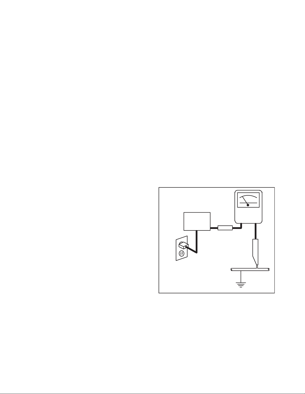
d. Leakage Current Hot Check - With the
instrument completely reassembled, plug the
AC line cord directly into a 120 V AC outlet. (Do
not use an isolation transformer during this
test.) Use a leakage current tester or a
metering system that complies with American
National Standards Institute (ANSI) C101.1
Leakage Current for Appliances and
Underwriters Laboratories (UL) 1410, (50.7).
With the instrument AC switch first in the on
position and then in the off position, measure
from a known earth ground (metal water pipe,
conduit, etc.) to all exposed metal parts of the
instrument (antennas, handle brackets, metal
cabinet, screw heads, metallic overlays, control
shafts, etc.), especially any exposed metal
parts that offer an electrical return path to the
chassis. Any current measured must not
exceed 0.5 milli-ampere. Reverse the
instrument power cord plug in the outlet and
repeat the test.
READING SHOULD
NOT BE ABOVE 0.5 mA
LEAKAGE
DEVICE
BEING
TESTED
TEST ALL EXPOSED
METAL SURFACES
ALSO TEST WITH
PLUG REVERSED
USING AC
ADAPTER PLUG
AS REQUIRED
ANY MEASUREMENTS NOT WITHIN THE
LIMITS SPECIFIED HEREIN INDICATE A
POTENTIAL SHOCK HAZARD THAT MUST
BE ELIMINATED BEFORE RETURNING THE
INSTRUMENT TO THE CUSTOMER OR
BEFORE CONNECTING THE ANTENNA OR
ACCESSORIES.
2. Read and comply with all caution and safety-
related notes on or inside the receiver cabinet, on
the receiver chassis, or on the Liquid Crystal
Panel.
CURRENT
TESTER
+
EARTH
GROUND
_
2-1 LTVN_ISP
Page 6

3. Design Alteration Warning - Do not alter or add
to the mechanical or electrical design of this TV
receiver. Design alterations and additions,
including, but not limited to circuit modifications
and the addition of items such as auxiliary audio
and/or video output connections, might alter the
safety characteristics of this receiver and create a
hazard to the user. Any design alterations or
additions will void the manufacturer's warranty and
may make you, the servicer, responsible for
personal injury or property damage resulting
therefrom.
4. Hot Chassis Warning a. Some TV receiver chassis are electrically
connected directly to one conductor of the AC
power cord and maybe safety-serviced without
an isolation transformer only if the AC power
plug is inserted so that the chassis is
connected to the ground side of the AC power
source. To confirm that the AC power plug is
inserted correctly, with an AC voltmeter,
measure between the chassis and a known
earth ground. If a voltage reading in excess of
1.0 V is obtained, remove and reinsert the AC
power plug in the opposite polarity and again
measure the voltage potential between the
chassis and a known earth ground.
b. Some TV receiver chassis normally have 85V
AC(RMS) between chassis and earth ground
regardless of the AC plug polarity. This chassis
can be safety-serviced only with an isolation
transformer inserted in the power line between
the receiver and the AC power source, for both
personnel and test equipment protection.
c. Some TV receiver chassis have a secondary
ground system in addition to the main chassis
ground. This secondary ground system is not
isolated from the AC power line. The two
ground systems are electrically separated by
insulation material that must not be defeated or
altered.
5. Observe original lead dress. Take extra care to
assure correct lead dress in the following areas: a.
near sharp edges, b. near thermally hot parts-be
sure that leads and components do not touch
thermally hot parts, c. the AC supply, d. high
voltage, and, e. antenna wiring. Always inspect in
all areas for pinched, out of place, or frayed wiring.
Check AC power cord for damage.
6. Components, parts, and/or wiring that appear to
have overheated or are otherwise damaged
should be replaced with components, parts, or
wiring that meet original specifications.
Additionally, determine the cause of overheating
and/or damage and, if necessary, take corrective
action to remove any potential safety hazard.
7. Product Safety Notice - Some electrical and
mechanical parts have special safety-related
characteristics which are often not evident from
visual inspection, nor can the protection they give
necessarily be obtained by replacing them with
components rated for higher voltage, wattage, etc.
Parts that have special safety characteristics are
identified by a # on schematics and in parts lists.
Use of a substitute replacement that does not
have the same safety characteristics as the
recommended replacement part might create
shock, fire, and/or other hazards. The product's
safety is under review continuously and new
instructions are issued whenever appropriate.
Prior to shipment from the factory, our products
are strictly inspected to confirm they comply with
the recognized product safety and electrical codes
of the countries in which they are to be sold.
However, in order to maintain such compliance, it
is equally important to implement the following
precautions when a set is being serviced.
2-2 LTVN_ISP
Page 7

Precautions during Servicing
A. Parts identified by the # symbol are critical for
safety.
Replace only with part number specified.
B. In addition to safety, other parts and assemblies
are specified for conformance with regulations
applying to spurious radiation. These must also be
replaced only with specified replacements.
Examples: RF converters, RF cables, noise
blocking capacitors, and noise blocking filters, etc.
C. Use specified internal wiring. Note especially:
1) Wires covered with PVC tubing
2) Double insulated wires
3) High voltage leads
D. Use specified insulating materials for hazardous
live parts. Note especially:
1) Insulation Tape
2) PVC tubing
3) Spacers
4) Insulators for transistors.
E. When replacing AC primary side components
(transformers, power cord, etc.), wrap ends of
wires securely about the terminals before
soldering.
F. Observe that the wires do not contact heat
producing parts (heat sinks, oxide metal film
resistors, fusible resistors, etc.)
G. Check that replaced wires do not contact sharp
edged or pointed parts.
H. When a power cord has been replaced, check that
5~6 kg of force in any direction will not loosen it.
I. Also check areas surrounding repaired locations.
J. Use care that foreign objects (screws, solder
droplets, etc.) do not remain inside the set.
K. When connecting or disconnecting the internal
connectors, first, disconnect the AC plug from the
AC supply outlet.
L. When installing parts or assembling the cabinet
parts, be sure to use the proper screws and
tighten certainly.
2-3 LTVN_ISP
Page 8
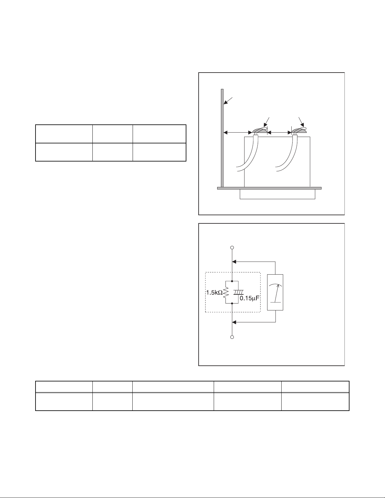
Safety Check after Servicing
Examine the area surrounding the repaired location for damage or deterioration. Observe that screws, parts and
wires have been returned to original positions. Afterwards, perform the following tests and confirm the specified
values in order to verify compliance with safety standards.
1. Clearance Distance
When replacing primary circuit components, confirm
specified clearance distance (d) and (d') between
soldered terminals, and between terminals and
surrounding metallic parts. (See Fig. 1)
Table 1: Ratings for selected area
Chassis or Secondary Conductor
Primary Circuit
AC Line Voltage Region
110 to 130 V
Note: This table is unofficial and for reference only. Be
sure to confirm the precise values.
U.S.A. or
Canada
Clearance
Distance (d), (d’)
≥ 3.2 mm
(0.126 inches)
2. Leakage Current Test
Confirm the specified (or lower) leakage current
between B (earth ground, power cord plug prongs) and
externally exposed accessible parts (RF terminals,
antenna terminals, video and audio input and output
terminals, microphone jacks, earphone jacks, etc.) is
lower than or equal to the specified value in the table
below.
Measuring Method: (Power ON)
Insert load Z between B (earth ground, power cord plug
prongs) and exposed accessible parts. Use an AC
voltmeter to measure across both terminals of load Z.
See Fig. 2 and following table.
d' d
Fig. 1
Exposed Accessible Part
Z
AC Voltmeter
(High Impedance)
Earth Ground
B
Power Cord Plug Prongs
Fig. 2
Table 2: Leakage current ratings for selected areas
AC Line Voltage Region Load Z Leakage Current (i) Earth Ground (B) to:
110 to 130 V
Note: This table is unofficial and for reference only. Be sure to confirm the precise values.
U.S.A. or
Canada
0.15 µF CAP. & 1.5 kΩ
RES. Connected in parallel
2-4 LTVN_ISP
i ≤ 0.5 mA rms
Exposed accessible
parts
Page 9
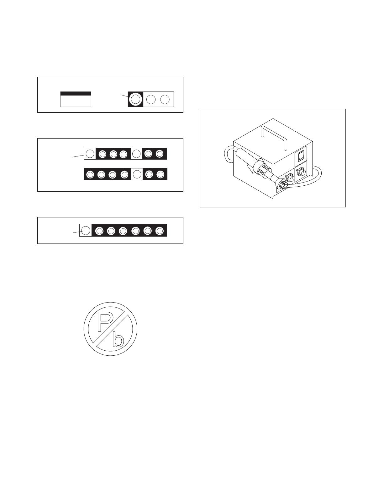
STANDARD NOTES FOR SERVICING
Circuit Board Indications
1. The output pin of the 3 pin Regulator ICs is
indicated as shown.
To p Vi ew
Out
2. For other ICs, pin 1 and every fifth pin are
indicated as shown.
Pin 1
3. The 1st pin of every male connector is indicated as
shown.
Pin 1
Input
In
Bottom View
5
10
Pb (Lead) Free Solder
Pb free mark will be found on PCBs which use Pb
free solder. (Refer to figure.) For PCBs with Pb free
mark, be sure to use Pb free solder. For PCBs
without Pb free mark, use standard solder.
Pb free mark
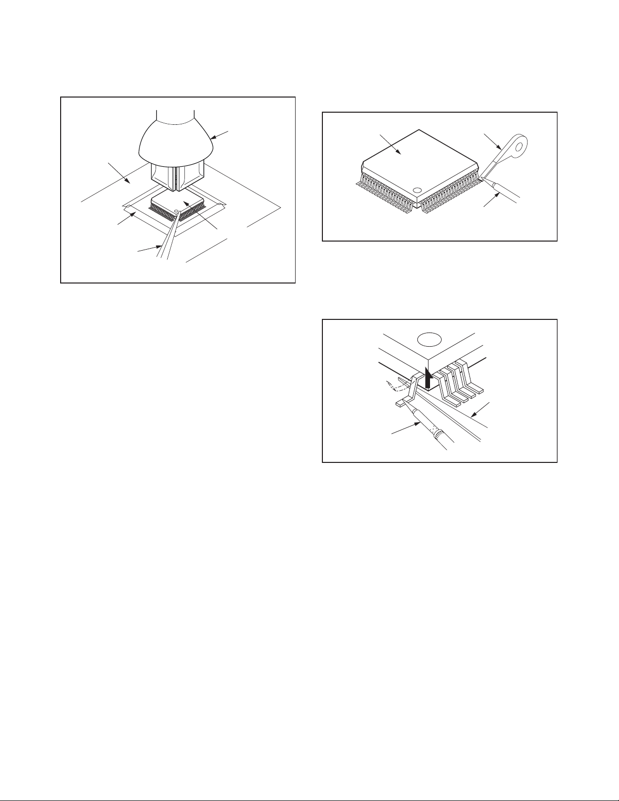
How to Remove / Install Flat Pack-IC
1. Removal
With Hot-Air Flat Pack-IC Desoldering Machine:
1. Prepare the hot-air flat pack-IC desoldering
machine, then apply hot air to the Flat Pack-IC
(about 5 to 6 seconds). (Fig. S-1-1)
Fig. S-1-1
2. Remove the flat pack-IC with tweezers while
applying the hot air.
3. Bottom of the flat pack-IC is fixed with glue to the
CBA; when removing entire flat pack-IC, first apply
soldering iron to center of the flat pack-IC and heat
up. Then remove (glue will be melted). (Fig. S-1-6)
4. Release the flat pack-IC from the CBA using
tweezers. (Fig. S-1-6)
CAUTION:
1. The Flat Pack-IC shape may differ by models. Use
an appropriate hot-air flat pack-IC desoldering
machine, whose shape matches that of the Flat
Pack-IC.
2. Do not supply hot air to the chip parts around the
flat pack-IC for over 6 seconds because damage
to the chip parts may occur. Put masking tape
around the flat pack-IC to protect other parts from
damage. (Fig. S-1-2)
3-1 TVN_SN
Page 10
3. The flat pack-IC on the CBA is affixed with glue, so
be careful not to break or damage the foil of each
pin or the solder lands under the IC when
removing it.
With Soldering Iron:
1. Using desoldering braid, remove the solder from
all pins of the flat pack-IC. When you use solder
flux which is applied to all pins of the flat pack-IC,
you can remove it easily. (Fig. S-1-3)
CBA
Masking
Ta pe
Tweezers
Hot-air
Flat Pack-IC
Desoldering
Machine
Flat Pack-IC
Fig. S-1-2
Flat Pack-IC
Desoldering Braid
Soldering Iron
Fig. S-1-3
2. Lift each lead of the flat pack-IC upward one by
one, using a sharp pin or wire to which solder will
not adhere (iron wire). When heating the pins, use
a fine tip soldering iron or a hot air desoldering
machine. (Fig. S-1-4)
Sharp
Pin
Fine Tip
Soldering Iron
3. Bottom of the flat pack-IC is fixed with glue to the
CBA; when removing entire flat pack-IC, first apply
soldering iron to center of the flat pack-IC and heat
up. Then remove (glue will be melted). (Fig. S-1-6)
4. Release the flat pack-IC from the CBA using
tweezers. (Fig. S-1-6)
Fig. S-1-4
3-2 TVN_SN
Page 11
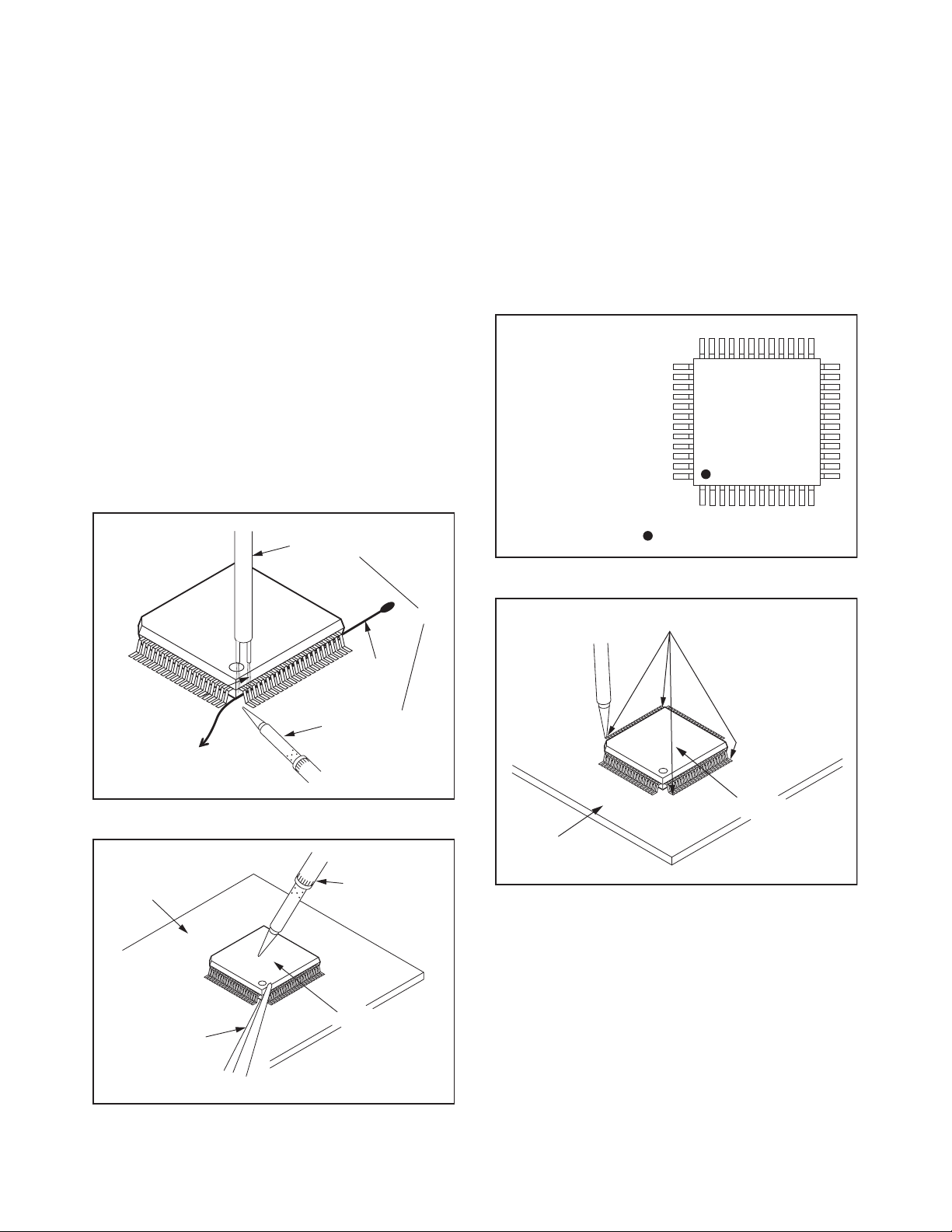
With Iron Wire:
1. Using desoldering braid, remove the solder from
all pins of the flat pack-IC. When you use solder
flux which is applied to all pins of the flat pack-IC,
you can remove it easily. (Fig. S-1-3)
2. Affix the wire to a workbench or solid mounting
point, as shown in Fig. S-1-5.
3. While heating the pins using a fine tip soldering
iron or hot air blower, pull up the wire as the solder
melts so as to lift the IC leads from the CBA
contact pads as shown in Fig. S-1-5.
4. Bottom of the flat pack-IC is fixed with glue to the
CBA; when removing entire flat pack-IC, first apply
soldering iron to center of the flat pack-IC and heat
up. Then remove (glue will be melted). (Fig. S-1-6)
5. Release the flat pack-IC from the CBA using
tweezers. (Fig. S-1-6)
Note: When using a soldering iron, care must be
taken to ensure that the flat pack-IC is not
being held by glue. When the flat pack-IC is
removed from the CBA, handle it gently
because it may be damaged if force is applied.
Hot Air Blower
2. Installation
1. Using desoldering braid, remove the solder from
the foil of each pin of the flat pack-IC on the CBA
so you can install a replacement flat pack-IC more
easily.
2. The “ I ” mark on the flat pack-IC indicates pin 1.
(See Fig. S-1-7.) Be sure this mark matches the
pin 1 on the PCB when positioning for installation.
Then presolder the four corners of the flat pack-IC.
(See Fig. S-1-8.)
3. Solder all pins of the flat pack-IC. Be sure that
none of the pins have solder bridges.
Example :
Pin 1 of the Flat Pack-IC
is indicated by a " " mark.
Fig. S-1-7
To Solid
Mounting Point
CBA
Tweezers
Iron Wire
Soldering Iron
Fig. S-1-5
Fine Tip
Soldering Iron
Flat Pack-IC
or
Presolder
Flat Pack-IC
CBA
Fig. S-1-8
Fig. S-1-6
3-3 TVN_SN
Page 12
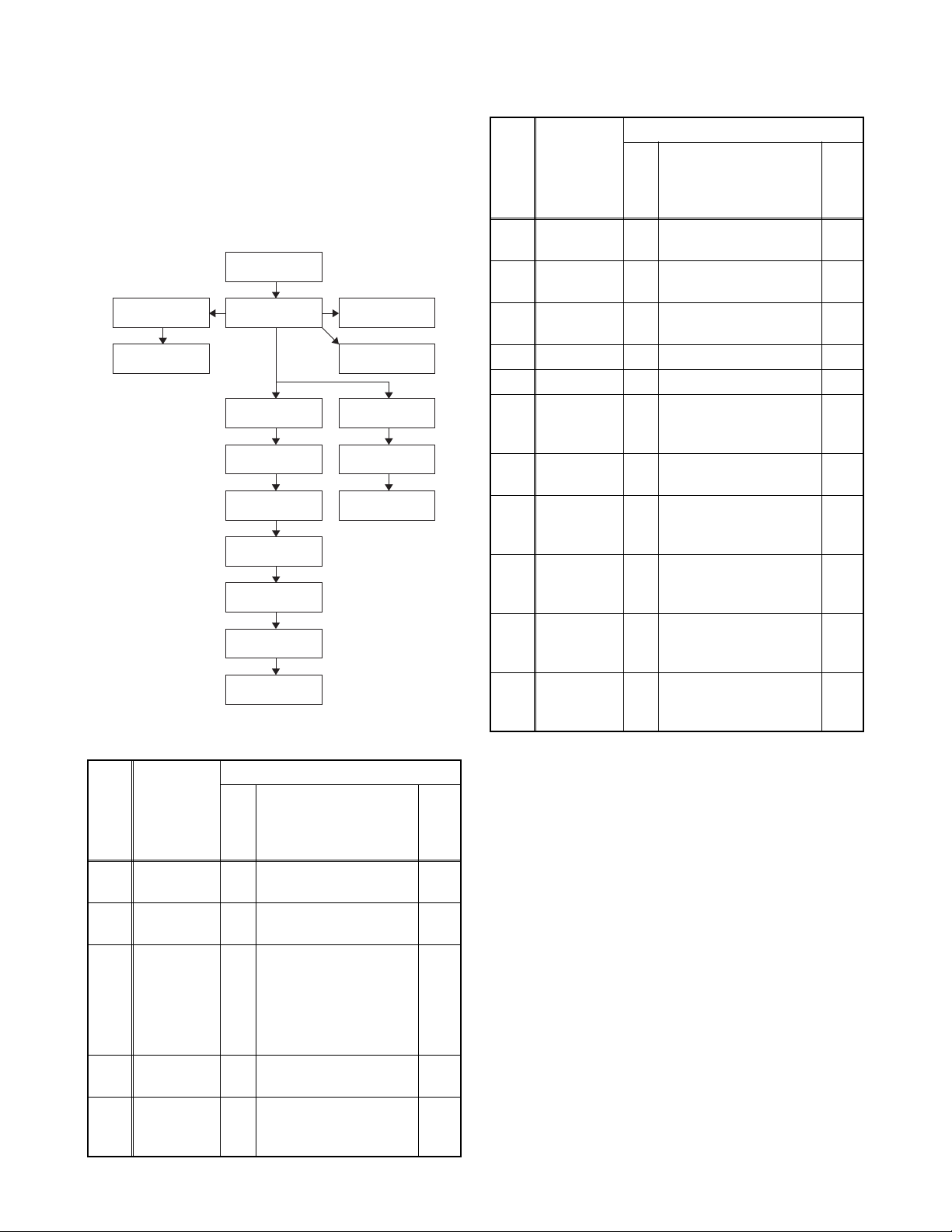
Instructions for Handling Semiconductors
Electrostatic breakdown of the semi-conductors may
occur due to a potential difference caused by
electrostatic charge during unpacking or repair work.
1. Ground for Human Body
Be sure to wear a grounding band (1 MΩ) that is
properly grounded to remove any static electricity that
may be charged on the body.
2. Ground for Workbench
Be sure to place a conductive sheet or copper plate
with proper grounding (1 MΩ) on the workbench or
other surface, where the semi-conductors are to be
placed. Because the static electricity charge on
clothing will not escape through the body grounding
band, be careful to avoid contacting semi-conductors
with your clothing.
<Incorrect>
<Correct>
1MΩ
CBA
Grounding Band
1MΩ
CBA
Conductive Sheet or
Copper Plate
3-4 TVN_SN
Page 13
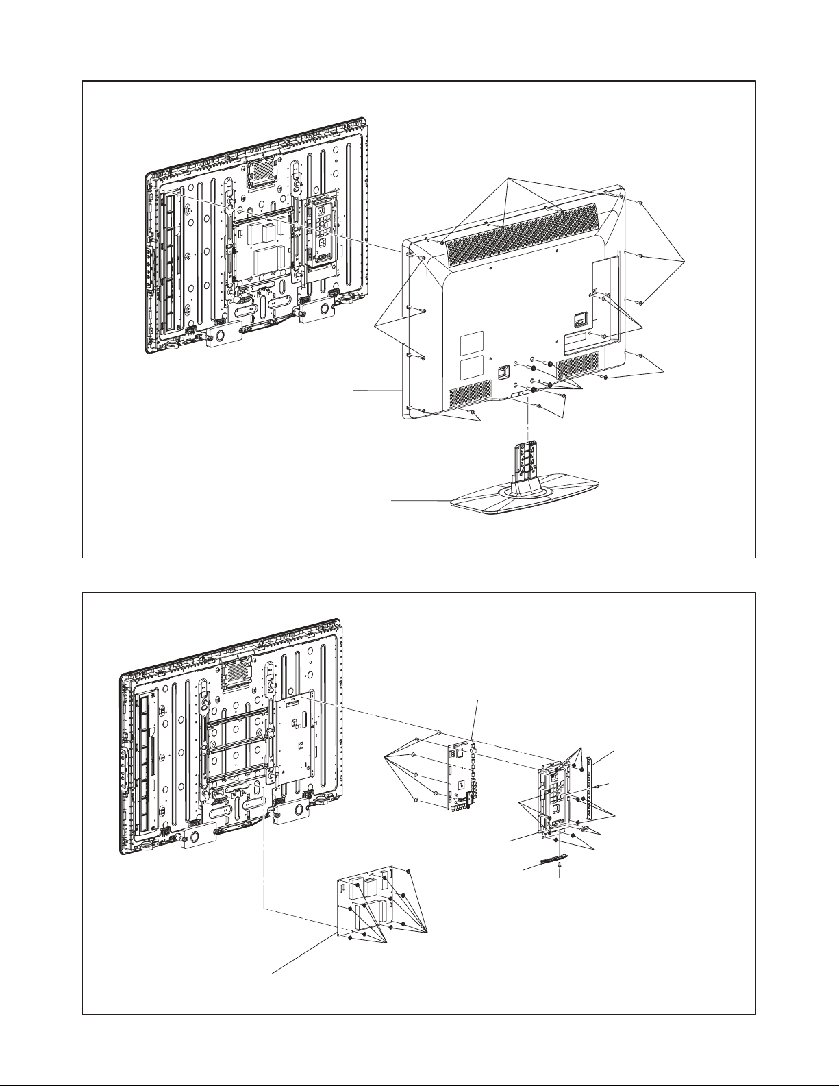
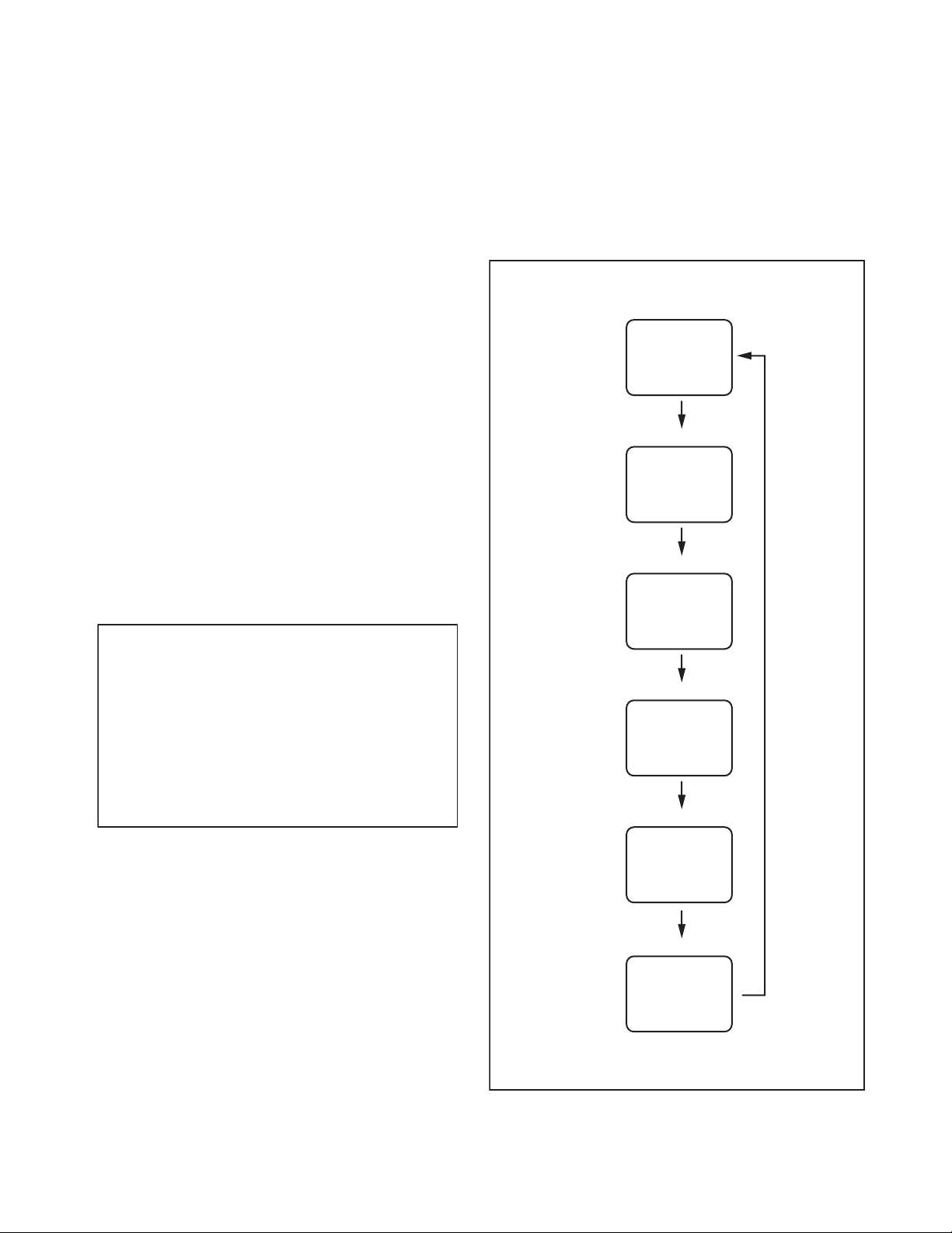
CABINET DISASSEMBLY INSTRUCTIONS
1. Disassembly Flowchart
This flowchart indicates the disassembly steps for the
cabinet parts, and the CBA in order to gain access to
item(s) to be serviced. When reassembling, follow the
steps in reverse order. Bend, route and dress the
cables as they were.
[1] Stand
Assembly
[9] Speaker-S
[10] Speaker
[2] Rear Cabinet
[5] Power Supply
CBA Unit
[7] PCB Holder
(D), (U)
[8] Wall Mount
Bracket
[11] Stand
Bracket
[14] Front Flare
[15] LCD Module
Assembly
[16] Front Cabinet
Assembly
[12] IR Sensor
CBA Unit
[13] Function
CBA Unit
[3] Shield Box
[4] Digital Main
CBA Unit
[6] Jack PCB
Holder
2. Disassembly Method
Removal
Step/
Loc.
Part
No.
Stand
[1]
Assembly
Rear
[2]
Cabinet
[3] Shield Box
Digital Main
[4]
CBA UnitD2D5
Power
[5]
Supply
CBA Unit
Remove/*Unhook/
Fig.
No.
Unlock/Release/
Unplug/Unclamp/
Note
Desolder
D1 4(S-1) ---
D1 16(S-2), 3(S-3) ---
2(S-4), 12(S-5), 2(H-1),
*CN3002, *CN3004,
D2
*CN3801, *CN3802,
D5
*CN4901, *CN4902,
Jack Holder(A),
Jack Holder(B)
6(S-6) ---
D2D511(S-7), *CN1, *CN4,
*CN5
---
---
Removal
Step/
Loc.
No.
Part
Fig.
Remove/*Unhook/
Unlock/Release/
No.
Unplug/Unclamp/
Note
Desolder
Jack PCB
[6]
Holder
PCB Holder
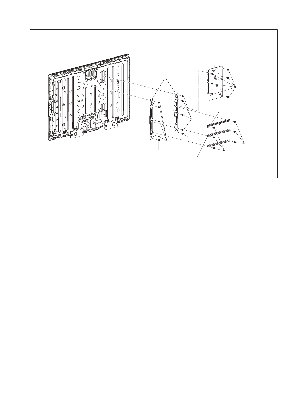
[7]
(D), (U)
Wall Mount
[8]
Bracket
D3 6(S-8) ---
D3 6(S-9) ---
D3 8(S-10), 2(S-11) ---
[9] Speaker-S D4 2(S-12), Desolder ---
[10] Speaker D4 4(S-13) ---
Stand
[11]
Bracket
IR Sensor
[12]
CBA UnitD4D5
Function
[13]
CBA UnitD4D5
2(S-14), 6(S-15),
D4
2(S-16),
AC Inlet Holder
*CN4051,
Sheet(Sensor)
Function Knob,
Knob Frame,
Sheet(Key)
---
---
---
15(S-17), 4(S-18),
[14] Front Flare D4
Boss, Boss(T),
---
Boss(W)
LCD
[15]
Module
D4 3(S-19) ---
Assembly
Front
[16]
Cabinet
D4 --------------- ---
Assembly
↓
(1)
↓
(2)
↓
(3)
↓
(4)
↓
(5)
Note:
(1) Order of steps in procedure. When reassembling,
follow the steps in reverse order. These numbers
are also used as the Identification (location) No. of
parts in figures.
(2) Parts to be removed or installed.
(3) Fig. No. showing procedure of part location
(4) Identification of parts to be removed, unhooked,
unlocked, released, unplugged, unclamped, or
desoldered.
P = Spring, L = Locking Tab, S = Screw,
H = Hex Screw, CN = Connector
* = Unhook, Unlock, Release, Unplug, or Desolder
e.g. 2(S-2) = two Screws (S-2),
2(L-2) = two Locking Tabs (L-2)
(5) Refer to the following "Reference Notes in the
Table."
4-1 PL10.8DC
Page 14
(S-2)
(S-2)
[2] Rear Cabinet
[1] Stand Assembly
(S-2)
(S-2)
(S-2)
[4] Digital Main CBA Unit
(S-3)
(S-2)
(S-1)
Fig. D1
[5] Power Supply CBA Unit
(S-6)
[3] Shield Box
Jack Holder(B)
(S-7)
(S-7)
(S-5)
(S-5)
(S-4)
Jack Holder(A)
(S-4)
(S-5)
(H-1)
(S-5)
Fig. D2
4-2 PL10.8DC
Page 15
[8] Wall Mount
Bracket
(S-10)
(S-11)
[7] PCB Holder (D)
[6] Jack PCB Holder
(S-8)
[7] PCB Holder (U)
(S-10)
(S-11)
(S-9)
(S-9)
Fig. D3
4-3 PL10.8DC
Page 16
[16] Front Cabinet Assembly
[15] LCD Module Assembly
[13] Function
CBA Unit
Sheet(Key)
Knob
Frame
Function
Knob
Boss
(S-19)
(S-17)
(S-17)
(S-18)
[11] Stand Bracket
Boss
(S-18)
Boss(T)
Boss(W)
Boss
Sheet(Sensor)
Desolder
(S-18)
Boss
[14] Front Flare
(S-17)
(S-18)
(S-15)
(S-16)
(S-17)
(S-17)
(S-17)
(S-17)
Boss(W)
Boss
[12] IR Sensor
CBA Unit
[9] Speaker-S
(S-15)
(S-16)
AC Inlet Holder
Boss
Desolder
(S-12)
(S-14)
(S-13)
[10] Speaker
[9] Speaker-S
(S-12)
(S-13)
[10] Speaker
Fig. D4
4-4 PL10.8DC
Page 17
TV Cable Wiring Diagram
To LCD Module Assembly
CN5
CN4
Power Supply CBA Unit
CN1
Function
CBA Unit
AC Cord
CN2
To LCD Module Assembly
CN4902
CN3002
CN4901
Digital Main
CBA Unit
CN3004
CN3801
CN3802
CN4001
IR Sensor CBA Unit
CN4051
To Speaker
CN4052
Fig. D5
4-5 PL10.8DC
Page 18
ELECTRICAL ADJUSTMENT INSTRUCTIONS
General Note: “CBA” is abbreviation for
“Circuit Board Assembly.”
Note: Electrical adjustments are required after
replacing circuit components and certain
mechanical parts. It is important to perform
these adjustments only after all repairs and
replacements have been completed.
Also, do not attempt these adjustments unless
the proper equipment is available.
Test Equipment Required
1. NTSC Pattern Generator (Color Bar W/White
Window, Red Color, Dot Pattern, Gray Scale,
Monoscope, Multi-Burst)
2. Remote control unit
3. Color Analyzer
How to set up the service mode:
Service mode:
1. Turn the power on.
2. Press [0], [6], [2], [5], [9], [6] and [INFO] buttons on
the remote control unit in this order. The following
screen appears.
1. Purity Check Mode
This mode cycles through full-screen displays of red,
green, blue, and white to check for non-active pixels.
1. Enter the Service mode.
2. Each time pressing [7] button on the remote
control unit, the display changes as follows.
Purity Check Mode
White mode
[7] button
[7] button
Black mode
[7] button
Red mode
"*" differs depending on the models.
[current]
File code :
Total checksum :
Panel-Option code :
[FRC]
SoftwareID :
Checksum :
BootID :
Tuner :
Safety :
EDID :
***-***-***-*
Push"0"key
**-***-***
Press "POWER" key to exit.
********-*****
****
***
*****
Safety_Non
Push"0"key
Lightsensor : **
[7] button
Green mode
[7] button
Blue mode
[7] button
White 20% mode
Note:
When entering this mode, the default setting is White mode.
3. To cancel or to exit from the Purity Check Mode,
press [PREV. CH] button.
5-1 PL10.8EA
Page 19

The White Balance Adjustment should be
performed when replacing the LCD Panel
or Digital Main CBA Unit.
2. White Balance Adjustment
Purpose: To mix red, green and blue beams correctly
for pure white.
Symptom of Misadjustment: White becomes bluish
or reddish.
Test Point
Screen
Pattern Generator,
Color analyzer
INPUT: WHITE 70%
1. Operate the unit for more than 60 minutes.
2. Input the White Raster (70%=70IRE).
3. Set the color analyzer to the CHROMA mode and
bring the optical receptor to the center on the
LCD-Panel surface after zero point calibration as
shown above.
Note: The optical receptor must be set
perpendicularly to the LCD Panel surface.
4. Enter the Service mode. Press [VOL] - button on the
remote control unit and select “C/D” mode.
Adj. Point Mode Input
[CH] + or -
button
M. EQ. Spec.
To avoid interference from ambinent
light, this adjustment should be
performed in a dark room.
Perpendicularity
L = 3 cm
C/D
x= 0.272 ± 0.003
y= 0.278 ± 0.003
Figure
Color Analyzer
White Raster
(APL 70%)
5. [CUTOFF]
Press [1] button to select “COR” for Red Cutoff
adjustment. Press [2] button to select “COG” for
Green Cutoff adjustment. Press [3] button to select
“COB” for Blue Cutoff adjustment.
[DRIVE]
Press [4] button to select “DR” for Red Drive
adjustment. Press [5] button to select “DG” for
Green Drive adjustment. Press [6] button to select
“DB” for Blue Drive adjustment.
6. Adjust the data of “1(COR)”, “2(COG)” and
“3(COB)” to 0 by using [CH] - or + button.
7. Adjust the data of “4(DR)”, “5(DG)” and “6(DB)” to
63 by using [CH] - or + button.
8. Adjust Drive so that the color temperature
becomes 12000°K (x
9. Adjust the highest data from the “4(DR)”, “5(DG)”
and “6(DB)” to 127 by using [CH] - or + button.
To adjust the rest of the two drive data, calculate
the data by the following method.
{ (128 + A) x 255 / (128 + B) } - 128
A: One of two data, except for the highest drive
data, you would like to calculate.
B: The highest drive data.
For example:
(When the current data says DR=70, DG=63 and
DB=59.)
1: Adjust the highest data to 127.
In this case, adjust the DR to 127.
2: Calculate the DG data.
{(128+63)x255/(128+70)}-128=117.9
The result for the DG data is 118.
3: Calculate the DB data.
{(128+59)x255/(128+70)}-128=112.8
The result for the DG data is 113.
10. To cancel or to exit from the White Balance
Adjustment, press [PREV. CH] button.
=
0.272 / y= 0.278 ±0.003).
5-2 PL10.8EA
Page 20

HOW TO INITIALIZE THE LCD TV
The purpose of initialization is to place the set in a new out of box condition. The customer will be prompted to
select a language and program channels after the set has been initialized.
To put the program back at the factory-default, initialize the LCD TV using the following procedure.
1. Turn the power on.
2. Enter the service mode.
- To cancel the service mode, press [ ] button on
the remote control unit.
3. Press [INFO] button on the remote control unit to
initialize the LCD television.
4. "INITIALIZED" will appear in the upper right of the
screen. "INITIALIZED" color will change to green
from red when initializing is completed.
5. Unplug the AC Cord.
6-1 PL10.12INT
Page 21

FIRMWARE RENEWAL MODE
Equipment Required
a. USB storage device
b. Remote Control Unit
Firmware Update Procedure
1. Turn the power off and unplug the AC Cord.
2. Insert the USB storage device to the USB port as
shown below.
USB port
USB storage
device
Rear Cabinet
(Files included in the USB storage device are
displayed.)
"*" differs depending on the models.
Select an upgrade file
Cancel
*****_******.upg
*****_******.upg
*****_******.upg
123
Note:
To cancel the update mode, select “Cancel” and
press the [OK] button.
10. Select the file and press [OK] button.
11. The update will start and the following will appear
on the screen.
"*" differs depending on the models.
Current Version:
New Version:
***-***-***-***-* ********-******
*******-***-*-***-****
3. Plug the AC Cord and turn the power on.
4. After few seconds, the menu mode will appear on
the screen.
Note:
After 30 seconds without an operation, the menu
mode will disappear automatically.
To display the menu mode again, press the
[MENU] button on the remote control unit.
5. Select “Setup” and press the [OK] button to display
the setup menu.
6. Select “Software update”.
7. Select “Updates”.
8. Select “USB”.
9. Press the [OK] button on the remote control unit to
enter the update mode.
Update file selection screen appears as follows.
Are you sure you want to update?
No Yes
Note:
If the above screen isn’t displayed, repeat from
step 1.
12. Select “Yes” and press the [OK] button to update.
Note:
Do not remove the USB storage device or turn the
TV off while update is in progress.
13. When the firmware update is completed, the
following will appear on the screen.
Update your TV with new software: Done
Software update is successful.
Please remove the USB storage device
and restart the TV set.
Remove the USB storage device from the USB
port.
Turn the power off and turn the power on again.
7-1 PL10.8FW
Page 22

FLOW CHART NO.1
The power cannot be turned on.
TROUBLESHOOTING
Is 5V voltage supplied to Pin(6) of CN3002 on the
Digital Main CBA Unit?
Ye s
When pressing power switch on the unit, LED is lighting
or flashing?
Ye s
When pressing power switch on the remote control unit,
LED is lighting or flashing?
Ye s
Is 3V voltage supplied to Pin(3) of CN3002 on the
Digital Main CBA Unit?
Ye s
Replace Power Supply CBA Unit.
FLOW CHART NO.2
The key operation is not functioning.
Is 3.3V voltage supplied to Pin(3) of CN3004 on the
Digital Main CBA Unit?
Ye s
Is 3.3V voltage supplied to Pin(1) of CN4001 on the
Function CBA Unit?
Ye s
Is the Pin(3) voltage of CN4001 0V when pressing
power switch?
Ye s
No
No
No
No
No
No
No
Replace Power Supply CBA Unit.
See FLOW CHART NO.2 <The key operation is not
functioning.>
See FLOW CHART NO.3 <No operation is possible
from remote control unit. (Operation is possible from
the unit.)>
Replace Digital Main CBA Unit.
Replace Digital Main CBA Unit.
Check the line between Pin(1) of CN4001 and Pin(3)
of CN3004, and service it if defective.
Replace Function CBA Unit.
Check the line between Pin(3) of CN4001 and Pin(6)
of CN3004, and service it if defective.
FLOW CHART NO.3
No operation is possible from remote control unit. (Operation is possible from the unit.)
Is 3.3V voltage supplied to Pin(3) of CN40
IR Sensor CBA Unit?
Ye s
Is the "L" pulse sent out Pin(2) of CN4052 on the
IR Sensor CBA Unit?
Ye s
Is the "L" pulse sent out Pin(2) of CN3004 on the
Digital Main CBA Unit?
Ye s
Replace Digital Main CBA Unit.
52 on the
No
No
No
Check AL+3.3V line and service it if defective.
Replace IR Sensor CBA Unit.
Check CL3004 and service it if defective.
8-1 PL10.4TR
Page 23

FLOW CHART NO.4
Picture does not appear normally.
Is 3V voltage supplied to Pin(1, 3) of CN3002 on the
Digital Main CBA Unit?
Ye s
Is 12V voltage supplied to Pin(10, 12, 13, 14) of
CN3002 on the Digital Main CBA Unit?
Ye s
Is 24V voltage supplied to Pin(1, 2, 3, 4,5) of CN4?
Ye s
CL4901, C
Module ma
Check and repla
FLOW CHART NO.5
Audio is not outputted normally.
Is 12V voltage supplied to Pin(10, 12, 13, 14
CN3002?
Are the audio signals outputted to Pin(1, 2) of CN
and Pin(1,
L4902, Digital Main CBA Unit or LCD
y be defective.
ce these parts.
) of
Ye s
3) of CN3802?
Ye s
3801
No
No
No
No
No
Replace Power Supply CBA Unit.
Replace Power Supply CBA Unit.
Replace Power Supply CBA Unit.
Replace Power Supply CBA Unit.
Replace Digital Main CBA Unit.
SP3801, SP3802, SP3803, SP3804, CL3801, C
CL3803 or CL3804 may be defectiv
Check and replace these parts.
e.
L3802,
8-2 PL10.4TR
Page 24

BLOCK DIAGRAMS
System Control Block Diagram
REMOTE
RS4051
LIGHT
IC4051
P-ON+5V
D4051
POWER
SENSOR
SENSOR
CN4052
LED155
REMOTE22
LIGHT77
KEY-IN166
CN3004
Q3001
CN4051
CN4001
IR SENSOR CBA UNIT
KEY-IN133
KEY SWITCH
FUNCTION CBA
UNIT
SCL
SDA
TU3001 (TUNER UNIT)
9
8
BACKLIGHT-SW1
CN3002
TO POWER SUPPLY
BLOCK DIAGRAM
(CN2)
BACKLIGHT-ADJ5
AL+5V6
P-ON+12V10
P-ON+12V12
P-ON+12V13
P-ON-H13
P-ON+12V14
Q4902
LCD+12V
SW+12V
P-ON+3.3V
P-ON+12V
+3.3V REG.
IC4604
VCC+1.8V
+1.8V REG.
IC3603
+2.7V REG.
IC4601
VCC+1.8V(1)
+1.8V REG.
IC4603
IC4602
VCC+1.25V(1)
VCC+1.25V
+1.25V REG.
+1.25V REG.
IC3604
IC3602
P-ON+5V
A+3.3V
+3.3V REG.
IC3607
+5V REG.
AL+1.25V
+1.25V REG.
IC3601
IC3606
AL+3.3V
+3.3V REG.
IC3101
(MAIN MICRO CONTROLLER)
(USB I/F)
IC3301
Q3002
1
USB(-)
CN3706
BUFFER
AM16
LIGHT
2
USB(+)
USB
AN23
REMOTE
USB-DP0
AP13
59
55PFL5705D/F7, 55PFL5705DV/F7
CN3705
CN3705
AL16
KEY-IN1
USB-DM0
AN13
58
USB
55
55
TX(+)
TX(+)
I/F
TX(-)
TX(-)
56
56
LAN
LAN
52
52
RX(+)
RX(+)
AL18
LED1
53
53
RX(-)
RX(-)
AP2
12
RESET HUB-RESET
XO
XI
61
60
X3301
25MHz
OSC
C31
TU-SCL
VGA-SCL
J5
VGA-SCL
VGA-SDA
B30
TU-SDA
COMP2-DET
VGA-SDA
AMP-MUTE
M5
G30
AP22
COMP2-DET
AMP-MUTE
TO VIDEO/AUDIO
BLOCK DIAGRAM
SWITCHING
SCL0
AN10
SDA0
AL8L1K1
LCD-ON AN8
H30BACKLIGHT-ADJ
AP21
P-ON-H1
SWITCHING
Q4901
AM21
LCD-P-ON
STM-SCL
STM-SDA
AP24
AM23
Q4601, Q4602
Q4611, Q4612
SWITCHING
AXI
B21
AXO
A21
OSCXO
OSCXI
AP17
AN17
DIGITAL MAIN CBA UNIT
SCL2
SDA2
12MHz
X3102
OSC
X3101
27.576MHz
6
5
SCL1
SDA1
XTAL-IN
AE13
27MHz
X4201
XTAL-OUT
AF13
OSC
SCL
SDA
IC3102 (MEMORY)
IC4201
(FRAME RATE CONTROL)
K2 L2
6
5
SCL
SDA
IC4203 (MEMORY)
OSC
9-1
PL10.8BLS
Page 25

Video/Audio Block Diagram
AUDIO SIGNAL
VIDEO SIGNAL
COM-VIDEO-Y-IN1
COM-VIDEO-Pb-IN1
COM-VIDEO-Y-IN2
COM-VIDEO-Pr-IN1
COM-VIDEO-Pb-IN2
VGA-R-IN
VGA-G-IN
COM-VIDEO-Pr-IN2
VGA-B-IN
VGA-HSYNC
VGA-VSYNC
TO DIGITAL
IF-AGC
DIF-OUT1
DIF-OUT2
SIGNAL PROCESS
BLOCK DIAGRAM
SIF
TU-CVBS
HDMI/PC-AUDIO(L)-IN
HDMI/PC-AUDIO(R)-IN
COMP-AUDIO(L)-IN1
COMP-AUDIO(R)-IN1
COMP-AUDIO(L)-IN2
COMP-AUDIO(R)-IN2
SPDIF
AMP(L)-
AMP(L)+
AMP(R)-
AMP(R)+
TO SYSTEM
VGA-SCL
VGA-SDA
CONTROL
BLOCK DIAGRAM
AMP-MUTE
COMP2-DET
WF1
COMPONENT
-Y-IN1
JK3001
JK3002
WF2
WF3
COMPONENT
-Pb-IN1
COMPONENT
-Pr-IN1
JK3003
WF1
COMPONENT
-Y-IN2
JK3006
JK3007
WF3
WF2
COMPONENT
-Pb-IN2
COMPONENT
-Pr-IN2
JK3008
123
131415
JK3701
PC-RGB
IN
12
TU3001
(TUNER UNIT)
12
13
14
IF-AGC
DIF-OUT1
DIF-OUT2
Q3003
BUFFER
19
VIDEO
16
SIF
HDMI/PC-
JK3011
JK3004
AUDIO-IN
WF4
COMPONENT-
AUDIO(L)-IN1
JK3005
COMPONENT-
AUDIO(R)-IN1
JK3009
WF4
COMPONENT-
AUDIO(L)-IN2
JK3010
BUFFER
JK3012
COMPONENT-
AUDIO(R)-IN2
Q3807
DIGITAL
AUDIO-OUT
(COAXIAL)
9
PWM
IC3801 (AUDIO AMP)
23,24
SP3803
854
GENE.
/GAIN CTL
DRIVE2
13,14
2
CN3801
SP(L)+
SP3801
PWM
47,48
1
SP(L)-
GENE.
DRIVE1
/GAIN CTL
MUTE CONTROL
37,38
CN3802
3
1
3
SP(R)-
SP(R)+
SP3802
DIGITAL MAIN CBA UNIT
SP3804
SPEAKER
SPEAKER
L-CH
R-CH
9-2 PL10.8BLV
Page 26

Digital Signal Process Block Diagram
LCD MODULE
ASSEMBLY
LVDS-TX2-1(-)40
LVDS-TX2-1(+)39
LVDS-TX2-0(-)42
LVDS-TX2-0(+)41
LVDS-TX2-2(-)38
LVDS-TX2-2(+)37
LVDS-TX2-3(-)32
LVDS-TX2-3(+)31
LVDS-TX2-4(-)30
LVDS-TX2-4(+)29
LVDS-TX4-0(-)27
LVDS-TX4-0(+)26
LVDS-TX4-1(-)25
LVDS-TX4-1(+)24
LVDS-TX4-2(-)23
LVDS-TX4-2(+)22
LVDS-TX4-3(-)17
LVDS-TX4-3(+)16
LVDS-TX4-4(-)15
LVDS-TX4-4(+)14
LVDS-TX2CLK(-)35
LVDS-TX2CLK(+)34
LVDS-TX4CLK(-)20
LVDS-TX4CLK(+)19
LVDS-TX1-1(-)30
LVDS-TX1-0(-)32
LVDS-TX1-0(+)31
LVDS-TX1-1(+)29
LVDS-TX1-2(-)28
LVDS-TX1-2(+)27
LVDS-TX1-3(-)22
LVDS-TX1-3(+)21
LVDS-TX1-4(-)20
LVDS-TX1-4(+)19
LVDS-TX3-0(-)17
LVDS-TX3-0(+)16
LVDS-TX3-1(-)15
LVDS-TX3-1(+)14
LVDS-TX3-2(-)13
LVDS-TX3-2(+)12
LVDS-TX3-3(-)7
LVDS-TX3-3(+)6
LVDS-TX3-4(-)5
LVDS-TX3-4(+)4
LVDS-TX1CLK(-)25
LVDS-TX1CLK(+)24
LVDS-TX3CLK(-)10
LVDS-TX3CLK(+)9
AUDIO SIGNAL
VIDEO SIGNAL
IC4201 (FRAME RATE CONTROL)
IC3101 (DIGITAL SIGNAL PROCESS)
VGA-HSYNC
VGA-VSYNC
A2
B3
D12
CN4901
A14
AF17
B32
D9
D11
B14
AE17
A32
D4
C14
AD17
B33
D5
A/D
D14
AC17
A33
CN4902
A9
B9
C9
A12
A21
B12
AE15
E34
A15
C12
AD15
F33
B21
D12
LVD S
OUTPUT
DATA
INPUT
LATCH
LVD S
RX
AF20
AE20
AC15
F34
H33
H34
DEMODULATOR
/MPEG DECODER
IF-AGC
A31
D19
D18
C21
AD20
J33
D21
AC20
J34
B20
AF19
K33
A17
C20
AE19
K34
C23
A19
AF18
M33
C24
B19
AE18
M34
A23
B23
C19
AD18
N33
D19
AC18
N34
AUDIO I/F
E31
E12
AD16
D33
C26
B13
C13
AF16
AF15
AE16
E33
C33
C34
CONVERTER
SW
A6
D6
D7
D8
D26
E13
AC16
D34
E20
AD19
L33
D24
D25
E21
AC19
L34
DIGITAL
A25
A11
SIGNAL
PROCESS
A26
B11
C11
D11
B10
C10
DATA
PROCESSING
AUDI O
DECODER
D9
A18
GAMMA
CORRECTOR
B18
FRC
P1
C18
LINE BUFFER
P2
D18
B17
A16
B16
E10
E11
E18
D16
E19
VIDEO
DECODER
DATA(0-15)
IC4401
(DDR2 SDRAM)
IC3403
DATA(0-15)
(DDR2 SDRAM)
79461
JK3702
DATA0(-)
DATA0(+)
DATA(16-31)
IC4402
ADDESS(0-12)
(DDR2 SDRAM)
IC3401
ADDESS(0-12)
(DDR2 SDRAM)
HDMI-IN4
DATA1(-)
DATA1(+)
DATA2(+)
ADDESS(0-12)
DATA(16-31)
ADDESS(0-12)
3
101216
DATA2(-)
CLOCK(-)
CLOCK(+)
IC4202
(NAND FLASH MEMORY)
IC3104
(NAND FLASH MEMORY)
15
HDMI-DATA
HDMI-CLOCK
DATA(0-7)
DATA(0-7)
C17
C16
HDMI
I/F
L1
N1
L2
N2
M1
M2
VGA-HSYNC
DIGITAL MAIN CBA UNIT
VGA-R-IN
VGA-VSYNC
VGA-G-IN
VGA-B-IN
COM-VIDEO-Y-IN1
TU-CVBS
COM-VIDEO-Y-IN2
COM-VIDEO-Pr-IN1
COM-VIDEO-Pb-IN1
COM-VIDEO-Pr-IN2
COM-VIDEO-Pb-IN2
DIF-OUT1
DIF-OUT2
IF-AGC
TO VIDEO/AUDIO
BLOCK DIAGRAM
SIF
AMP(L)+
AMP(L)-
AMP(R)+
AMP(R)-
SPDIF
HDMI/PC-AUDIO(L)-IN
HDMI/PC-AUDIO(R)-IN
COMP-AUDIO(L)-IN2
COMP-AUDIO(L)-IN1
COMP-AUDIO(R)-IN1
IC3201 (HDMI SW)
COMP-AUDIO(R)-IN2
DATA0(+)
JK3705
9-3
DATA0(-)
7 68
677069727166652930
DATA1(+)
DATA1(-)
DATA2(+)
DATA2(-)
HDMI-DATA
HDMI-CLOCK
CLOCK(+)
94613
CLOCK(-)
101216
HDMI-IN1
56575859606162
4365872
DATA0(+)
DATA0(-)
DATA1(+)
JK3704
79461
15
HDMI
DATA1(-)
63
SW
DATA2(+)
DATA2(-)
HDMI-IN2
CLOCK(+)
CLOCK(-)
3
101216
1
33
HDMI-DATA
HDMI-CLOCK
222124232625201943
34
141316151817121139
DATA0(+)
JK3703
79461
15
DATA0(-)
DATA1(+)
DATA1(-)
DATA2(+)
DATA2(-)
HDMI-DATA
HDMI-CLOCK
CLOCK(+)
CLOCK(-)
3
101216
HDMI-IN3
PL10.8BLD
44
40
15
Page 27

Power Supply Block Diagram
CN2
TO SYSTEM
CONTROL
AL+5V9
P-ON+12V
1-4
BLOCK
DIAGRAM
BACKLIGHT-ADJ
BACKLIGHT-SW
10
14
(CN3002)
P-ON-H1
12
LCD MODULE
ASSEMBLY
NOTE:
The voltage for parts in hot circuit is measured using
hot GND as a common terminal.
3
4
T901
10
For continued protection against risk of fire,
replace only with same type 5 A, 250V fuse.
IC901
(SWITCHING CONTROL)
CAUTION ! :
ATTENTION : Utiliser un fusible de rechange de même type de 5A, 250V.
9
5
7
SWITCHING
6
2
CONTROL
5A/250V
POWER SUPPLY CBA UNIT
Q905
Q910
Q210
1
(ISOLATOR)
PC902
4
2
IN
IC902
(LINEAR REGULATOR)
4
5,6
L800A
1,2
7,8
OUT
4
SCR210
3 2
1
EN
9
6
3
1
Q601B
T601
5
4
14
12710
SWITCHING
Q601A
(FEED BACK)
PC901
4
L800B
7,8
14
3 2
Q903
Q902
5,6
1,2
2
1
7
5
Q904
CN4
13
11
SWITCHING
CT601
PANEL+24V1-5
8
2
4
1
BACKLIGHT-ADJ14BACKLIGHT-SW
12
14
PC601
(FEED BACK)
3
2
PANEL+24V1-5
CN5
3 2
HOT COLD
Q801B
BRIDGE
RECTIFIER
BD1
LINE
FILTER
FL2
IC801
LINE
FILTER
FL1
F1
5A/250V
1
AC
AC601
CN1
INLET
AC CORD
3
HOT CIRCUIT. BE CAREFUL.
CAUTION !
Fixed voltage (or Auto voltage selectable) power supply circuit is used in this unit.
If Main Fuse (F1) is blown , check to see that all components in the power supply
circuit are not defective before you connect the AC plug to the AC power supply.
Otherwise it may cause some components in the power supply circuit to fail.
(SWITCHING CONTROL)
SWITCHING
14
SWITCHING
7
9-4
SWITCHING
Q801A
11
CONTROL
8
VCC
SCR601
6
5
RESONANT
CONTROL
9
14
15
11612
IC601
(HIGH-VOLTAGE
RESONANT CONTROL)
Q802
Q800
11
HIGH-
VOLTAGE
8
12
PL10.8BLP
Page 28

SCHEMATIC DIAGRAMS AND TEST POINTS
Standard Notes
WARNING
Many electrical and mechanical parts in this chassis
have special characteristics. These characteristics
often pass unnoticed and the protection afforded by
them cannot necessarily be obtained by using
replacement components rated for higher voltage,
wattage, etc. Replacement parts that have these
special safety characteristics are identified in this
manual and its supplements; electrical components
having such features are identified by the mark “#” in
the schematic diagram and the parts list. Before
replacing any of these components, read the parts list
in this manual carefully. The use of substitute
replacement parts that do not have the same safety
characteristics as specified in the parts list may create
shock, fire, or other hazards.
Notes:
1. Do not use the part number shown on these
drawings for ordering. The correct part number is
shown in the parts list, and may be slightly
different or amended since these drawings were
prepared.
2. All resistance values are indicated in ohms
(K = 10
3. Resistor wattages are 1/4W or 1/6W unless
otherwise specified.
4. All capacitance values are indicated in µF
(P = 10
5. All voltages are DC voltages unless otherwise
specified.
6.
This schematic diagrams are masterized version
that should cover the entire PL10.8 chassis models.
Thus some parts in detail illustrated on this
schematic diagrams may vary depend on the
model within the PL10.8 chassis.
Please refer to the parts lists for each models.
7. The Circuit Board layout illustrated on this service
manual is the latest version for this chassis at the
moment of making this service manual.
Depend on the mass production date of each
model, the actual layout of each Board may differ
slightly from this version.
3
, M = 106).
-6
µF).
10-1 PL10.8SC
Page 29

LIST OF CAUTION, NOTES, AND SYMBOLS USED IN THE SCHEMATIC DIAGRAMS ON
r
THE FOLLOWING PAGES:
1. CAUTION:
CAUTION: FOR CONTINUED PROTECTION AGAINST RISK OF FIRE, REPLACE ONLY WITH SAME
TYPE_A,_V FUSE.
ATTENTION: UTILISER UN FUSIBLE DE RECHANGE DE MÊME TYPE DE_A,_V.
2. CAUTION:
Fixed Voltage (or Auto voltage selectable) power supply circuit is used in this unit.
If Main Fuse (F1) is blown, first check to see that all components in the power supply circuit are not defective
before you connect the AC plug to the AC power supply. Otherwise it may cause some components in the
power supply circuit to fail.
3. Note:
1. Do not use the part number shown on the drawings for ordering. The correct part number is shown in the
parts list, and may be slightly different or amended since the drawings were prepared.
2. To maintain original function and reliability of repaired units, use only original replacement parts which are
listed with their part numbers in the parts list section of the service manual.
4. Voltage indications on the schematics are as shown below:
Plug the TV power cord into a standard AC outlet.:
2
(Unit: Volt)
1
5.0 5.0
3
Power on mode
5. How to read converged lines
1-D3
Distinction Area
Line Number
(1 to 3 digits)
Examples:
1. "1-D3" means that line number "1" goes to the line numbe
"1" of the area "D3".
2. "1-B1" means that line number "1" goes to the line number
"1" of the area "B1".
6. Test Point Information
: Indicates a test point with a jumper wire across a hole in the PCB.
: Used to indicate a test point with a component lead on foil side.
: Used to indicate a test point with no test pin.
: Used to indicate a test point with a test pin.
Voltage
Indicates that the voltage
is not consistent here.
3
2
1
AREA D3
1-B1
AREA B1
1-D3
ABCD
10-2 PL10.8SC
Page 30

Digital Main 1 Schematic Diagram
1 NOTE:
The order of pins shown in this diagram is different from that of actual IC3101.
IC3101 is divided into five and shown as IC3101 (1/7) ~ IC3101 (7/7) in this Digital Main Schematic Diagram Section.
10-3
PL10.8SCD1
Page 31

Digital Main 2 Schematic Diagram
1 NOTE:
The order of pins shown in this diagram is different from that of actual IC3101.
IC3101 is divided into five and shown as IC3101 (1/7) ~ IC3101 (7/7) in this Digital Main Schematic Diagram Section.
10-4
PL10.8SCD2
Page 32

Digital Main 3 Schematic Diagram
1 NOTE:
The order of pins shown in this diagram is different from that of actual IC3101.
IC3101 is divided into five and shown as IC3101 (1/7) ~ IC3101 (7/7) in this Digital Main Schematic Diagram Section.
10-5
PL10.8SCD3
Page 33

Digital Main 4 Schematic Diagram
1 NOTE:
The order of pins shown in this diagram is different from that of actual IC3101.
IC3101 is divided into five and shown as IC3101 (1/7) ~ IC3101 (7/7) in this Digital Main Schematic Diagram Section.
10-6
PL10.8SCD4
Page 34

Digital Main 5 Schematic Diagram
1 NOTE:
The order of pins shown in this diagram is different from that of actual IC3101.
IC3101 is divided into five and shown as IC3101 (1/7) ~ IC3101 (7/7) in this Digital Main Schematic Diagram Section.
10-7
PL10.8SCD5
Page 35

Digital Main 6 Schematic Diagram
1 NOTE:
The order of pins shown in this diagram is different from that of actual IC3101.
IC3101 is divided into five and shown as IC3101 (1/7) ~ IC3101 (7/7) in this Digital Main Schematic Diagram Section.
10-8
PL10.8SCD6
Page 36

Digital Main 7 Schematic Diagram
1 NOTE:
The order of pins shown in this diagram is different from that of actual IC3101.
IC3101 is divided into five and shown as IC3101 (1/7) ~ IC3101 (7/7) in this Digital Main Schematic Diagram Section.
2 NOTE:
The order of pins shown in this diagram is different from that of actual IC4201.
IC4201 is divided into five and shown as IC4201 (1/5) ~ IC4201 (5/5) in this Digital Main Schematic Diagram Section.
10-9
PL10.8SCD7
Page 37

Digital Main 8 Schematic Diagram
2 NOTE:
The order of pins shown in this diagram is different from that of actual IC4201.
IC4201 is divided into five and shown as IC4201 (1/5) ~ IC4201 (5/5) in this Digital Main Schematic Diagram Section.
10-10
PL10.8SCD8
Page 38

Digital Main 9 Schematic Diagram
2 NOTE:
The order of pins shown in this diagram is different from that of actual IC4201.
IC4201 is divided into five and shown as IC4201 (1/5) ~ IC4201 (5/5) in this Digital Main Schematic Diagram Section.
10-11
PL10.8SCD9
Page 39

Digital Main 10 Schematic Diagram
2 NOTE:
The order of pins shown in this diagram is different from that of actual IC4201.
IC4201 is divided into five and shown as IC4201 (1/5) ~ IC4201 (5/5) in this Digital Main Schematic Diagram Section.
10-12
PL10.8SCD10
Page 40

Digital Main 11 Schematic Diagram
2 NOTE:
The order of pins shown in this diagram is different from that of actual IC4201.
IC4201 is divided into five and shown as IC4201 (1/5) ~ IC4201 (5/5) in this Digital Main Schematic Diagram Section.
10-13
PL10.8SCD11
Page 41

Digital Main 12 Schematic Diagram
10-14
PL10.8SCD12
Page 42

Digital Main 13 Schematic Diagram
10-15
PL10.8SCD13
Page 43

Power Supply Schematic Diagram
CAUTION !
Fixed voltage (or Auto voltage selectable) power supply circuit is used in this unit.
If Main Fuse (F1) is blown , check to see that all components in the power supply
circuit are not defective before you connect the AC plug to the AC power supply.
Otherwise it may cause some components in the power supply circuit to fail.
5A/250V
CAUTION ! :
ATTENTION : Utiliser un fusible de rechange de même type de 5A, 250V.
For continued protection against risk of fire,
replace only with same type 5 A, 250V fuse.
NOTE:
The voltage for parts in hot circuit is measured using
hot GND as a common terminal.
10-16
PL10.8SCP
Page 44

Function Schematic Diagram
10-17
PL10.8SCF
Page 45

IR Sensor Schematic Diagram
10-18
PL10.8SCIR
Page 46

Power Supply CBA Top View
CAUTION !
Fixed voltage (or Auto voltage selectable) power supply circuit is used in this unit.
If Main Fuse (F1) is blown , check to see that all components in the power supply
circuit are not defective before you connect the AC plug to the AC power supply.
Otherwise it may cause some components in the power supply circuit to fail.
5A/250V
CAUTION ! :
ATTENTION : Utiliser un fusible de rechange de même type de 5A, 250V.
For continued protection against risk of fire,
replace only with same type 5 A, 250V fuse.
NOTE:
The voltage for parts in hot circuit is measured using
hot GND as a common terminal.
Because a hot chassis ground is present in the power supply
circuit, an isolation transformer must be used when repairing.
Also, in order to have the ability to increase the input slowly,
when troubleshooting this type of power supply circuit,
a variable isolation transformer is required.
10-19
DPS-55
Page 47

Power Supply CBA Bottom View
CAUTION !
Fixed voltage (or Auto voltage selectable) power supply circuit is used in this unit.
If Main Fuse (F1) is blown , check to see that all components in the power supply
circuit are not defective before you connect the AC plug to the AC power supply.
Otherwise it may cause some components in the power supply circuit to fail.
5A/250V
CAUTION ! :
ATTENTION : Utiliser un fusible de rechange de même type de 5A, 250V.
For continued protection against risk of fire,
replace only with same type 5 A, 250V fuse.
NOTE:
The voltage for parts in hot circuit is measured using
hot GND as a common terminal.
Because a hot chassis ground is present in the power supply
circuit, an isolation transformer must be used when repairing.
Also, in order to have the ability to increase the input slowly,
when troubleshooting this type of power supply circuit,
a variable isolation transformer is required.
10-20
DPS-55
Page 48

WAVEFORMS
AUDIO
0.1V
0.5m
VIDEO-Pr
0.2V
VIDEO-Pb
0.2V
VIDEO-Y
0.2V
WF1 ~ WF4 = Waveforms to be observed at
Waveform check points.
(Shown in Schematic Diagram.)
Input: NTSC Color Bar Signal (with 1kHz Audio Signal)
WF1
VIDEO-Y
WF2
VIDEO-Pb
JK3001, JK3006
0.2V
JK3002, JK3007
0.2V
2020µ
2020µ
s
s
WF3
VIDEO-Pr
WF4
AUDIO
JK3003, JK3008
0.2V
JK3004, JK3009
0.1V
2020µ
0.5m
s
s
PL10.8WF11-1
Page 49

WIRING DIAGRAM
9NU8
7
LVDS-TX3-3(+)
LVDS-TX3-4(-)
LVDS-TX3-4(+)
6
5
4
6NU5NU4NU3NU2
FRC-CTRL1
BACKLIGHT-ADJ
LVDS-TX3CLK(+)
GND7LVDS-TX3-3(-)
9
8
12NU11NU10
FRC-CTRL4
LVDS-TX3-1(+)
LVDS-TX3-2(-)
LVDS-TX3-2(+)
GND10LVDS-TX3CLK(-)
14
13
12
11
16
15
14
13
GND
LVDS-TX4-4(-)
LVDS-TX4-3(+)
LVDS-TX4-4(+)
LVDS-TX3-0(+)
LVDS-TX3-1(-)
16
15
19
18
17
GND
LVDS-TX4-3(-)
LVDS-TX4CLK(+)
LVDS-TX1-4(-)
LVDS-TX1-4(+)
GND17LVDS-TX3-0(-)
20
19
18
23
22
21
20
GND
LVDS-TX4-2(-)
LVDS-TX4-2(+)
LVDS-TX4CLK(-)
LVDS-TX1CLK(+)
GND22LVDS-TX1-3(-)
LVDS-TX1-3(+)
24
23
21
24
25
26
27
LVDS-TX4-1(-)
LVDS-TX4-0(-)
LVDS-TX4-1(+)
LVDS-TX4-0(+)
LVDS-TX1CLK(-)
GND27LVDS-TX1-2(+)
LVDS-TX1-2(-)
LVDS-TX1-1(+)
25
26
28
29
AC601
AC CORD
28
29
30
31
32
33
34
GND
LVDS-TX2-4(+)
LVDS-TX1-1(-)
30
GND
LVDS-TX2-4(-)
LVDS-TX2-3(-)
LVDS-TX2-3(+)
LVDS-TX2CLK(+)
LVDS-TX1-0(+)
LVDS-TX1-0(-)
GND34GND35GND36NU37LCD+12V38LCD+12V39LCD+12V40LCD+12V41LCD+12V
31
32
33
35
36
37
38
GND
LVDS-TX2-2(-)
LVDS-TX2-2(+)
LVDS-TX2CLK(-)
39
40
41
42
LVDS-TX2-1(-)
LVDS-TX2-0(-)
LVDS-TX2-1(+)
LVDS-TX2-0(+)
43
GND44GND45GND
46NU47
LCD+12V48LCD+12V49LCD+12V50LCD+12V51LCD+12V
1
CN4901
NU
CL4901
FRC-CTRL5
LCD MODULE ASSEMBLY
GND2NU1NU
CL4902
3
CN4902
SP3803
CL3803
SPEAKER
L-CH
SP3801
CL3801
1
SP(L)-
CN3801
2
SP(L)+
SP3804
CL3804
SPEAKER
R-CH
SP3802
CL3802
1
2
NU
SP(R)-
CN3802
3
SP(R)+
CN4052
1
CL3004
GND
1
CN3004
2
REMOTE
2
1
CN4001CN4051
CL4001
AL+3.3V
1
3
4
AL+3.3V
P-ON+5V
3
4
FUNCTION CBA
UNIT
2
3
GND
KEY-IN1
2
3
IR SENSOR
CBA UNIT
5
6
7
LED1
KEY-IN1
LIGHT
5
6
7
CL601
CN1
CL401
PANEL+24V2PANEL+24V3PANEL+24V4PANEL+24V5PANEL+24V
1
321
CN4
TUNER UNIT
CN2
14
CL3002
BACKLIGHT-SW
1
CN3002
GND7GND8GND9GND10GND
6
10
11
12
13
BACKLIGHT-ADJ(PWM)
GND3P-ON-H1
BACKLIGHT-ADJ(DC)
5
4
2
POWER SUPPLY
AL+5V
6
NU
BACKLIGHT-SW
12
11
CBA UNIT
GND8GND7GND
9
CL402
PANEL+24V2PANEL+24V3PANEL+24V4PANEL+24V5PANEL+24V
BACKLIGHT-ADJ(PWM)
BACKLIGHT-ADJ(DC)
1
13
14
CN5
P-ON+12V
GND
P-ON+12V
12
11
10
123546789
P-ON+12V
P-ON+12V
14
13
GND7GND8GND9GND10GND
6
COMPONENT
-Y-IN1
COMPONENT
-Pb-IN1
COMPONENT
-Pr-IN1
COMPONENT-
AUDIO(L)-IN1
COMPONENT
-Y-IN2
COMPONENT-
AUDIO(R)-IN1
COMPONENT
-Pb-IN2
COMPONENT
-Pr-IN2
DIGITAL MAIN CBA UNIT
COMPONENT-
AUDIO(L)-IN2
COMPONENT-
AUDIO(R)-IN2
HDMI/PC-
AUDIO-IN
DIGITAL
AUDIO-OUT
(COAXIAL)
D-SUB
CONNECTOR
HDMI-
CONNECTOR-1
HDMI-
CONNECTOR-2
HDMI-
CONNECTOR-3
HDMI-
CONNECTOR-4
55PFL5705D/F7,
USB JACK
PL10.8WI12-1
55PFL5705DV/F7
LAN
CONNECTOR
Page 50

Cabinet
EXPLODED VIEWS
CL4901
Front Cabinet Assembly
B49
B49
L22
L22
L31
B6
L20
A16
L31
L31
L20
L22
B49
B12
L20
B8
Power Supply CBA Unit
L20
L20
B9
B31
L5
CL3002
L20
L20
CL4902
L5
CL401
CL402
CL3004
Digital Main CBA Unit
TH4201
B18
B31
B18
B18
TH3101
TH3801
B1
A10
L5
L5
L5
A9
L12
L5
L13
L5
L12
LCD-1
L30
Function CBA Unit
See Electrical Parts List
for parts with this mark.
A4
A5
CL4001
B41
B49
L31
L22
B49
B29
B52
L31
B28
B49
B42
IR Sensor CBA Unit
B52
B29
L22
B5
L31
B28
CL3803
B49
L31
SP3803
L20
L31
L17
L20
CL3801
SP3801
L16
B10
SP3804
SP3802
L5
CL601
X11
L16
CL3804
L17
CL3802
L31
L31
L31
L14
L31
A2
L31
55PFL5705D/F7,
55PFL5705DV/F7
L31
L36
A18
A19
A12
S6
55PFL5505D/F7
A20
A17
A22
13-1 PL10.8CEX
Page 51

Packing
55PFL5505D/F7,
55PFL5705D/F7
X3 X6 X7 X12 X8 X10 X4
S6
55PFL5505D/F7,
55PFL5705D/F7
55PFL5705DV/F7
AC601
S13
S3
X1
X2
S6
S6
55PFL5705DV/F7
Carton
Sealing
Ta pe
X1
X2 X13
55PFL5705D/F7,
55PFL5705DV/F7
FRONT
55PFL5705DV/F7
X19 X20X18
X21
55PFL5705DV/F7
S13
S11
Carton Sealing
Ta pe
S1
S5
Some Ref. Numbers are
not in sequence.
S11
S12
S4
Carton Sealing Tape
S6
FRONT
S2
Carton Sealing
Ta pe
Strapping Strip
13-2 PL10.8PEX
Page 52

PARTS LIST [55PFL5505D/F7]
Mechanical Parts
PRODUCT SAFETY NOTE: Products marked with a
# have special characteristics important to safety.
Before replacing any of these components, read
carefully the product safety notice in this service
manual. Don't degrade the safety of the product
through improper servicing.
NOTE: Parts that are not assigned part numbers
(---------) are not available.
Ref. No. Description Part No.
FRONT CABINET ASSEMBLY A01R5UF 1EM025185
A2 REAR CABINET A01R5UF 1EM024857
A4 FUNCTION KNOB A01P5UF 1EM327097
A5 KNOB FRAME A01P5UF 1EM223763
A9 JACK HOLDER(A) 5K A01P5UF 1EM223750
A10 JACK HOLDER(B) 5K A01P5UF 1EM327099
A12# RATING LABEL A01R5UF ---------A16 FRONT FLARE A01R5UF 1EM024858
A17 JACK LABEL-A A01P5UF 1EM430739
A18 JACK LABEL-B A01P5UF 1EM430740
A19 JACK LABEL-C A01P5UF 1EM430741
A22 STAND ASSEMBLY(SWIVEL) A01R5UF 1EMN26119
B1 SHIELD BOX 5K A01P5UF 1EM024855
B5 STAND BRACKET A01R5UF 1EM024865
B6 WALL MOUNT BRACKET A01R5UF 1EM124135
B8 PCB HOLDER(U) 40W5K A01P5UF 1EM223751
B9 PCB HOLDER(D) 40W5K A01P5UF 1EM223752
B10 AC INLET HOLDER 5K A01P5UF 1EM327102
B12 JACK PCB HOLDER A01R5UF 1EM124137
B18 GASKET(15X4X2) A01Q0UF 1EM430743
B28 BOSS(W) A01P5UF 1EM327100
B29 BOSS(T) A01P5UF 1EM327101
B31 GASKET(60X4XT2) A01P5UF 1EM430738
B41 SHEET(KEY) A01P5UF 1EM431457
B42 SHEET(SENSOR) A01P5UF 1EM431458
B49 BOSS A01R5UF 1EM430398
B52 CLOTH(10X30XT0.5) B5900UA 0EM404486
CL401 WIRE ASSEMBLY 14PIN 14PIN/410MM/RED
CL402 WIRE ASSEMBLY 10PIN-14PIN 10P-14P/
CL601 WIRE ASSEMBLY 2PIN 2PIN/200MM/WHITE
CL3002 WIRE ASSEMBLY 14PIN 14PIN/150MM/RED
CL3004 WIRE ASSEMBLY 7PIN 7PIN/490MM/RED
CL3801 WIRE ASSEMBLY 2PIN 2PIN/270MM/RED
CL3802 WIRE ASSEMBLY 2PIN 2PIN/820MM/RED
CL3803 WIRE ASSEMBLY 2PIN 2PIN/370MM/RED
CL3804 WIRE ASSEMBLY 2PIN 2PIN/370MM/RED
CL4001 WIRE ASSEMBLY 3PIN 3PIN/960MM/RED
CL4901 WIRE ASSEMBLY 51PIN 51PIN/471MM WX1A01R5-102
CL4902 WIRE ASSEMBLY 41PIN 41PIN/471MM WX1A01R5-101
BLK
410MM/Y/B
BLK
BLK
BLACK
BLACK
BLACK
BLACK
BLACK
BLACK
WX1A01R5-303
WX1A01R5-304
WX1A01P5-308
WX1A01R5-307
WX1A01R5-301
WX1A01R5-305
WX1A01R5-306
WX1A01R5-309
WX1A01R5-309
WX1A01R5-302
Ref. No. Description Part No.
L5 ASSEMBLED SCREW ( D9 M3X6 ) A71F0UH 1EM424392B
L12 SCREW S-TIGHT M3X8 BIND HEAD+ GBHS3080
L13 HEX SCREW #4-40 7MM 1EM430139
L14 DOUBLE SEMS SCREW M5X20 M5X20 FPH35200
L16 ASSEMBLED SCREW (D16.5/M4X14)
L17 SCREW P-TIGHT 3X12 BIND HEAD+ BLK GBHP3120
L20 DOUBLE SEMS SCREW M4X6 M4X6 FPJ34060
L22 DOUBLE SEMS SCREW M4X10 + BLK FPH34100
L30 SCREW P-TIGHT M4X18 BIND HEAD+ GBHP4180
L31 SCREW P-TIGHT 3X14 WASHER HEAD+ GCHP3140
L36 DOUBLESEMS SCREW M3X8 A01P7UH 1EM432184
LCD-1 LCD MODULE/55W LTA550HJ01 UDULCD0SM005
SP3801 SPEAKER MAGNETIC SB-05N43C DS06520XQ002
SP3802 SPEAKER MAGNETIC SB-05N43B DS06520XQ001
SP3803 SPEAKER MAGNETIC S025FH02 DS06220XQ001
SP3804 SPEAKER MAGNETIC S025FH02 DS06220XQ001
TH3101 THERMAL SHEET TMS-L-3 20X20HC XK10000X4009
TH3801 THERMAL SHEET TMS-L-3 7X7HC XK10000X4010
TH4201 THERMAL SHEET TMS-L-3 20X20HC XK10000X4009
A73F2FP
1EM425499
PACKING
S1 CARTON(T) A01R5UF 1EM328141B
S2 CARTON(B) A01R5UF 1EM328144A
S3 STYROFOAM TOP A01R5UF 1EM025765
S4 STYROFOAM BOTTOM A01R5UF 1EM025766
S5 SET BAG A01R5UF 1EM328143
S6 SERIAL NO.LABEL A01Q0UF ---------S11 STYROFOAM CENTER A01R5UF 1EM025767
S12 SET SHEET A01R5UF 1EM328337
ACCESSORIES
AC601# CORD W/O A GND WIRE UL/CSA/ 162/NO/
X1 OENERS MANUAL BAG A91H5UF 1EM429581
X2# OWNERS MANUAL A01P5UF 1EMN26019A
X3 REMOTE CONTROL UNIT YKF255-007 URMT42JHG002
X4 BATTERY R03-B500/01S XB0M451CZB01
X6 QUICK START GUIDE A01P5UF 1EMN26020
X7 REGISTRATION CARD A01P5UF 1EMN26042A
X8 CHILD SAFETY SHEET A91H5UF 1EMN25001
X10 WALL MOUNT INSTRUCTION A01P5UF 1EMN26041A
X11 CONNECTION GUIDE A01P5UF 1EM327858
X12 CABLE MANAGEMENT TIE(BLACK) A01F2UH 1EM431197
BLACK
WAV0162LW001
20100517 14-1 A01R5CA
Page 53

Electrical Parts
PRODUCT SAFETY NOTE: Products marked with a
# have special characteristics important to safety.
Before replacing any of these components, read
carefully the product safety notice in this service
manual. Don't degrade the safety of the product
through improper servicing.
NOTES:
1. Parts that are not assigned part numbers (---------)
are not available.
2. Tolerance of Capacitors and Resistors are noted
with the following symbols.
C.....±0.25% D.....±0.5% F.....±1%
G.....±2% J......±5% K.....±10%
M.....±20% N.....±30% Z.....+80/-20%
POWER SUPPLY CBA UNIT
Ref. No. Description Part No.
POWER SUPPLY CBA UNIT UPBPSPDEL003
DIGITAL ASSEMBLY
Ref. No. Description Part No.
DIGITAL ASSEMBLY
Consists of the following
DIGITAL MAIN CBA UNIT
FUNCTION CBA UNIT
IR SENSOR CBA UNIT
A01R5MMA-003
A01R5MMA-003-DM
A01R5MMA-003-FN
A01R5MMA-003-IR
20100517 14-2 A01R5EL
Page 54

PARTS LIST [55PFL5705D/F7]
Mechanical Parts
PRODUCT SAFETY NOTE: Products marked with a
# have special characteristics important to safety.
Before replacing any of these components, read
carefully the product safety notice in this service
manual. Don't degrade the safety of the product
through improper servicing.
NOTE: Parts that are not assigned part numbers
(---------) are not available.
Different parts from the original model
55PFL5505D/F7
Ref. No. Description Part No.
A9 JACK HOLDER(A) 5K A01P6UF 1EM327157
A12# RATING LABEL A01R6UF ---------A17 Not used
A20 JACK LABEL-D A01P6UF 1EM430897
S1 CARTON(T) A01R6UF 1EM328518A
X2# OWNERS MANUAL A01P6UF 1EMN26141
X3 REMOTE CONTROL UNIT YKF255-008 URMT42JHG003
X11 CONNECTION GUIDE A01P6UF 1EM327859
X13 NETFLIX GUIDE A01P6UF 1EMN26319
20100622 14-3 A01R6CA
Page 55

Electrical Parts
PRODUCT SAFETY NOTE: Products marked with a
# have special characteristics important to safety.
Before replacing any of these components, read
carefully the product safety notice in this service
manual. Don't degrade the safety of the product
through improper servicing.
NOTES:
1. Parts that are not assigned part numbers (---------)
are not available.
2. Tolerance of Capacitors and Resistors are noted
with the following symbols.
C.....±0.25% D.....±0.5% F.....±1%
G.....±2% J......±5% K.....±10%
M.....±20% N.....±30% Z.....+80/-20%
Different parts from the original model
55PFL5505D/F7
Ref. No. Description Part No.
DIGITAL ASSEMBLY
Consists of the following
DIGITAL MAIN CBA UNIT
FUNCTION CBA UNIT
IR SENSOR CBA UNIT
A01R6MMA-004
A01R6MMA-004-DM
A01R6MMA-004-FN
A01R6MMA-004-IR
20100622 14-4 A01R6EL
Page 56

PARTS LIST [55PFL5705DV/F7]
Mechanical Parts
PRODUCT SAFETY NOTE: Products marked with a
# have special characteristics important to safety.
Before replacing any of these components, read
carefully the product safety notice in this service
manual. Don't degrade the safety of the product
through improper servicing.
NOTE: Parts that are not assigned part numbers
(---------) are not available.
Different parts from the original model
55PFL5505D/F7
Ref. No. Description Part No.
A9 JACK HOLDER(A) 5K A01P6UF 1EM327157
A12# RATING LABEL A01R9UF ---------A17 Not used
A20 JACK LABEL-D A01P6UF 1EM430897
S1 CARTON (T) A01R9UF 1EM329477
S6 SERIAL NO. LABEL A01PKUF ---------S13 CARTON LABEL A01PKUF ---------X2# OWNERS MANUAL A01PKUF 1EMN27003
X3 REMOTE CONTROL UNIT YKF255-008 URMT42JHG003
X6 QUICK START GUIDE A01PKUF 1EMN27004
X11 CONNECTION GUIDE A01P6UF 1EM327859
X13 NETFLIX GUIDE A01P6UF 1EMN26319
X18 WIRELESS LAN ADAPTOR WU5205 UWLUSBACM001
X19 LEAFLET A01P6UF 1EMN27040
X20 VUDU SHEET A01PKUF 1EMN27000
X21 DONGLE LABEL A01PKUF ----------
20100922 14-5 A01R9CA
Page 57

Electrical Parts
PRODUCT SAFETY NOTE: Products marked with a
# have special characteristics important to safety.
Before replacing any of these components, read
carefully the product safety notice in this service
manual. Don't degrade the safety of the product
through improper servicing.
NOTES:
1. Parts that are not assigned part numbers (---------)
are not available.
2. Tolerance of Capacitors and Resistors are noted
with the following symbols.
C.....±0.25% D.....±0.5% F.....±1%
G.....±2% J......±5% K.....±10%
M.....±20% N.....±30% Z.....+80/-20%
Different parts from the original model
55PFL5505D/F7
Ref. No. Description Part No.
DIGITAL ASSEMBLY
Consists of the following
DIGITAL MAIN CBA UNIT
FUNCTION CBA UNIT
IR SENSOR CBA UNIT
A01R9MMA-002
A01R9MMA-002-DM
A01R9MMA-002-FN
A01R9MMA-002-IR
20100922 14-6 A01R9EL
Page 58

Chassis PL10.8
• 2010-06-10 55PFL5505D/F7 added
• 2010-07-09 55PFL5705D/F7 added
• 2010-10-16 55PFL5705DV/F7 added
REVISION HISTORY
15-1 PL10.8REV
 Loading...