

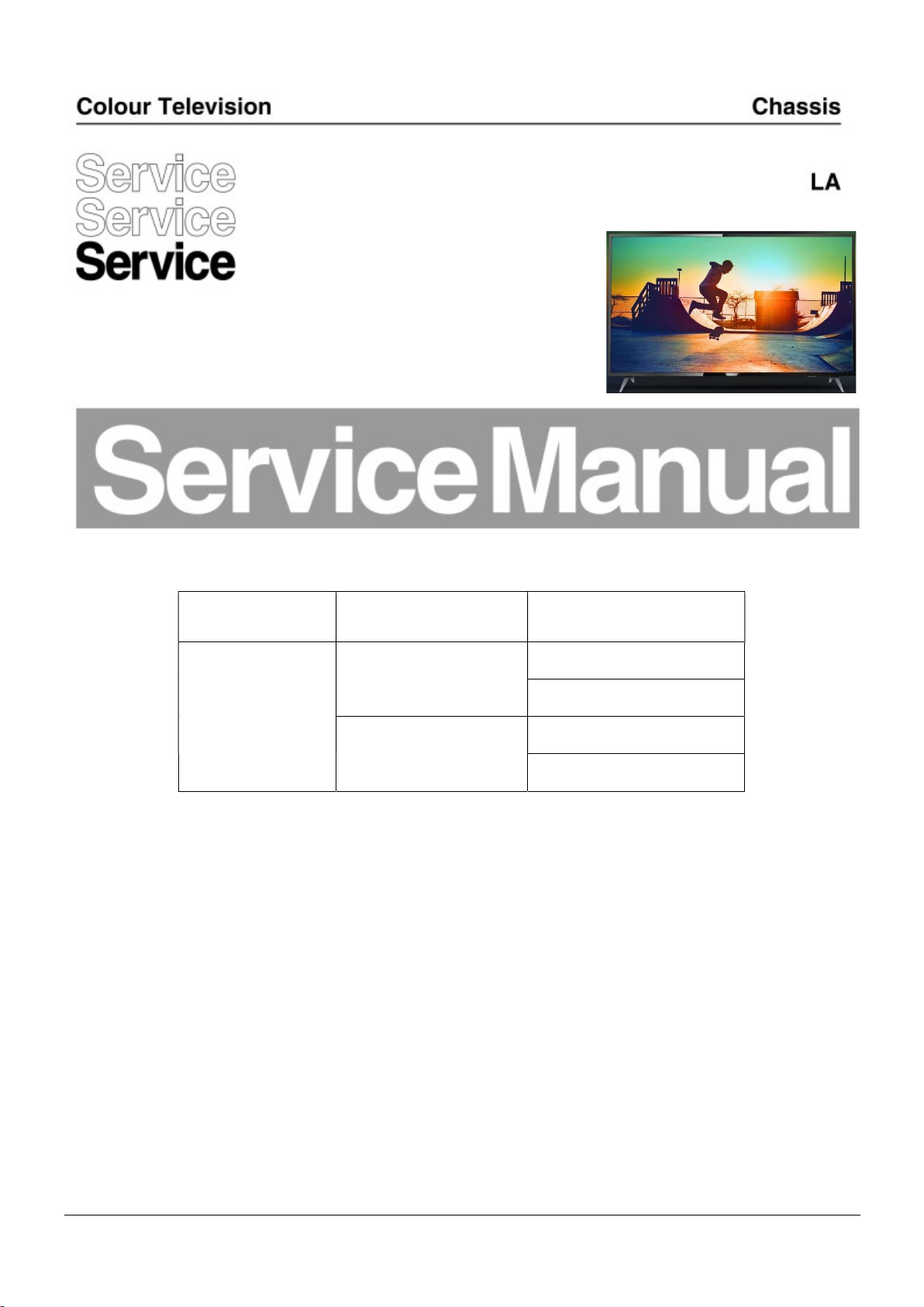
TPM18.6K
Chassis name
Platform Model name
50PUN6233/61
MTK5802
55PUN6233/61
TPM18.6K LA
55OLED873/61
MTK5802+NT72334
65OLED873/61
Published by Amy/SC 1811 Quality Subject to modification 3122 785 20700
2018 © TP Vision Netherlands B.V.
All rights reserved. Specifications are subject to change without notice. Trademarks are the
property of Koninklijke Philips Electronics N.V. or their respective owners.
TP Vision Netherlands B.V. reserves the right to change products at any time without being obliged to adjust
earlier supplies accordingly.
PHILIPS and the PHILIPS’ Shield Emblem are used under license from Koninklijke Philips Electronics N.V.
2018-Mar-16

1. Product information……….…………………………………………………………………………………3
2. Precautions, Notes, and Abbreviation List…………….………………………………………………5
3. Mechanical Instructions………………….……………………………………………………………….11
Cable dressing (50" 6233 series)……………………………………………………………………………11
Cable dressing (55" 6233 series)……………………………………………………………………………11
Cable dressing (55/65" OLED873 series)…………………………………………………………………12
Assembly/Panel Removal ……………………………………………………………………………………13
4. Service Modes…………….……………….……………….…………………………………………….….19
5. Software upgrading, Error Code and Panel Code………...………………………………………..23
6. Trouble Shooting……………………………………………...……………………………………………..28
7. Electrical Diagram…..……………………….………………………………………………………………31
8. IC Data Sheet……...…………………………………………………………………………………….…..37
9. Circuit Diagrams……………...…………………………………………………………………………….44
9.1 715G7374 PSU……………………………………………………………………..……………………44
9.2 715G8886 PSU……………………………………………………………………..……………………48
9.3 715G9309 PSU……………………………………………………………………..……………………52
9.4 715G8709 SSB……………………………………………………………………..……………………56
9.5 715G8885 SSB……………………………………………………………………..……………………75
9.6 715G8623 IR/LED Panel……………………………………………..………………………………100
9.7 715G8555 Keyboard control panel……………………………………………………………………101
9.8 715G6981 AMBI Panel……………………………………………..……………………………….102
9.9 715G7004 AMBI Panel……………………………………………..……………………………….104
9.10 715G7007 AMBI Panel……………………………………………..……………………………….106
9.11 715G8236 AMBI Panel……………………………………………..……………………………….108
9.12 715G9001 LED Panel……………………………………………..……………………………….110
10. Styling Sheet……………….………………….………………………………………………………….111
6233 series 50"……………………………………………………………………………………………….111
6233 series 55"……………………………………………………………………………………………….112
OLED873 series 55"…………………………………………………………………………………………113
OLED873 series 65"…………………………………………………………………………………………114
Published by Amy/SC 1811 Quality Subject to modification 3122 785 20700
2018 © TP Vision Netherlands B.V.
All rights reserved. Specifications are subject to change without notice. Trademarks are the
property of Koninklijke Philips Electronics N.V. or their respective owners.
TP Vision Netherlands B.V. reserves the right to change products at any time without being obliged to adjust
earlier supplies accordingly.
PHILIPS and the PHILIPS’ Shield Emblem are used under license from Koninklijke Philips Electronics N.V.
2018-Mar-16

1. Product information
Product information is subject to change without notice.
For detailed product information, please visit
www.philips.com/support
Display Resolution
Diagonal screen size
• 50PUN62x3 : 126 cm / 50 inch
• 55PUN62x3, OLED873 : 139 cm / 55 inch
• 65OLED873 : 164 cm / 65 inch
Display resolution
• 3840 x 2160
Reception
distorted picture or sound.
To avoid the malfunctioning of such a device, you can
set the signal quality to a level the device can handle.
If the device is not using Ultra HD signals, you can
switch off Ultra HD for this HDMI connection.
• The setting Optimal* allows maximum up to Ultra
HD (50Hz or 60Hz) RGB 4:4:4 or YCbCr
4:4:4/4:2:2/4:2:0 signals.
• The setting Standard allows maximum up to Ultra
HD (50Hz or 60Hz) YCbCr 4:2:0 signals.
• The setting Off is to watch videos with Full HD.
* Available when Source is set to HDMI 2 or HDMI 3
Component, Composite
Composite
• PAL, NTSC, SECAM
• Aerial input : 75 ohm coaxial (IEC75)
• Tuner bands : UHF, VHF
• ATSC
• Digital video playback : MPEG2 SD/HD (ISO/IEC
13818-2), MPEG4 SD/HD (ISO/IEC 14496-10), HEVC*
• Digital audio playback (ISO/IEC 13818-3)
Supported Input Resolution -
Video
Support Timing
Video support timing also includes field/frame rate
23.976Hz, 29.97Hz and 59.94Hz.
HDMI
• 480i - 24Hz, 25Hz, 30Hz, 50Hz, 60Hz
• 480p - 24Hz, 25Hz, 30Hz, 50Hz, 60Hz
• 576i - 24Hz, 25Hz, 30Hz, 50Hz, 60Hz
• 576p - 24Hz, 25Hz, 30Hz, 50Hz, 60Hz
• 720p - 24Hz, 25Hz, 30Hz, 50Hz, 60Hz
• 1080i - 24Hz, 25Hz, 30Hz, 50Hz, 60Hz
• 1080p - 24Hz, 25Hz, 30Hz, 50Hz, 60Hz
• 3840 x 2160p - 24Hz, 25Hz, 30Hz, 50Hz, 60Hz
HDMI - UHD
(Home) > Settings > All settings > General
settings > HDMI Ultra HD
This TV can display Ultra HD signals. Some devices connected with HDMI - do not recognise a TV with
Ultra HD and might not work correctly or show
Component
• 480i - 24Hz, 25Hz, 30Hz, 50Hz, 60Hz
• 480p - 24Hz, 25Hz, 30Hz, 50Hz, 60Hz
• 576i - 24Hz, 25Hz, 30Hz, 50Hz, 60Hz
• 576p - 24Hz, 25Hz, 30Hz, 50Hz, 60Hz
• 720p - 24Hz, 25Hz, 30Hz, 50Hz, 60Hz
• 1080i - 24Hz, 25Hz, 30Hz, 50Hz, 60Hz
• 1080p - 24Hz, 25Hz, 30Hz, 50Hz, 60Hz
Supported Input Resolution -
Computer
• 640 x 480 - 60Hz
• 800 x 600 - 60Hz
• 1024 x 768 - 60Hz
• 1280 x 800 - 60Hz
• 1280 x 960 - 60Hz
• 1280 x 1024 - 60Hz
• 1366 x 768 - 60Hz
• 1440 x 900 - 60Hz
• 1920 x 1080 - 60Hz
• 3840 x 2160 - 60Hz
Sound
• Incredible Surround
• Clear Sound
• Smart Sound
• Output power (RMS) :
50/55PUN62x3: 20W

55/65OLED873: 30W
• Dolby Audio ™
• DTS 2.0+ Digital out
Connectivity
50/55PUN62x3:
TV Side
• USB 2 - USB 2.0
• HDMI 3 in - MHL - UHD - HDR
• Headphones - Stereo mini-jack 3.5mm
TV Rear
• YPbPr : Y Pb Pr, Audio L/R
• CVBS : CVBS, Audio L/R (Shared with YPbPr)
TV Bottom
• Digital Audio out - Optical
• USB 1 - USB 3.0
• Network LAN - RJ45
• Antenna (75 ohm)
• HDMI 1 in - ARC - UHD
• HDMI 2 in - UHD – HDR
55/65OLED873:
TV Side
• USB 1 - USB 2.0
• USB 2 - USB 3.0
• Headphones - Stereo mini-jack 3.5mm
• HDMI 1 in - ARC - Ultra HD
• HDMI 2 in - Ultra HD - HDR
• HDMI 3 in - MHL - Ultra HD - HDR
• AV: AV, Audio L/R (Shared with YPbPr)
• Antenna (75 ohm)
Multimedia
Connections
• USB 2.0 / USB 3.0
• Ethernet LAN RJ-45
• Wi-Fi 802.11n (built-in)
Supported USB file systems
• FAT, NTFS
Playback formats
• Video Codec : AVI, MKV, HEVC, H.264/MPEG-4
AVC, MPEG1, MPEG2, MPEG4, WMV9/VC1, VP9
• Audio Codec : MP3, WAV, AAC, WMA (v2 up to
v9.2), WMA-PRO (v9 and v10)
• Subtitles :
- Format: SRT, SMI, SSA, SUB, ASS, TXT
- Character encodings : UTF-8, Central Europe and
Eastern Europe (Windows-1250), Cyrillic
(Windows-1251), Greek (Windows-1253), Turkish
(Windows-1254), Western Europe (Windows-1252)
• Image Codec : JPEG, GIF, PNG, BMP
Wi-Fi Certified
This TV supports Miracast certified devices.
Performance may vary, depending on the capabilities
of the mobile device and the software used.
Power
TV Bottom
• Digital Audio out - Optical
• Network LAN - RJ45
• YPbPr: Y Pb Pr, Audio L/R
• Mains power : AC 220-240V +/-10%
• Ambient temperature : 5°C to 35°C

2. Precautions, Notes, and Abbreviation List
tools. This will prevent any short circuits and the danger
of a circuit becoming unstable.
2.1 Safety Instructions
Safety regulations require the following during a repair:
• Connect the set to the Mains/AC Power via an isolation
transformer (> 800 VA).
• Replace safety components, indicated by the symbol △!,
only by components identical to the original ones. Any
other component substitution (other than original type)
may increase risk of fire or electrical shock hazard.
Safety regulations require that after a repair, the set must
be returned in its original condition. Pay in particular
attention to the following points:
• Route the wire trees correctly and fix them with the
mounted cable clamps.
• Check the insulation of the Mains/AC Power lead for
external damage.
• Check the strain relief of the Mains/AC Power cord for
proper function.
• Check the electrical DC resistance between the
Mains/AC Power plug and the secondary side (only for
sets that have a Mains/AC Power isolated power supply):
1. Unplug the Mains/AC Power cord and connect a wire
between the two pins of the Mains/AC Power plug.
2. Set the Mains/AC Power switch to the “on” position
(keep the Mains/AC Power cord unplugged!).
3. Measure the resistance value between the pins of the
Mains/AC Power plug and the metal shielding of the
tuner or the aerial connection on the set. The reading
should be between 4.5 MΩ and 12 MΩ.
4. Switch “off” the set, and remove the wire between the
two pins of the Mains/AC Power plug.
• Check the cabinet for defects, to prevent touching of any
inner parts by the customer.
!
2.2 Warnings
• All ICs and many other semiconductors are susceptible
to electrostatic discharges (ESD ). Careless handling
during repair can reduce life drastically. Make sure that,
during repair, you are connected with the same potential
as the mass of the set by a wristband with resistance.
Keep components and tools also at this same potential.
• Be careful during measurements in the high voltage
section.
• Never replace modules or other components while the
unit is switched “on”.
• When you align the set, use plastic rather than metal
2.3 Notes
2.3.1 General
• Measure the voltages and waveforms with regard to the
chassis (= tuner) ground ( ), or hot ground ( ),
depending on the tested area of circuitry. The voltages
and waveforms shown in the diagrams are indicative.
Measure them in the Service Default Mode with a colour
bar signal and stereo sound (L: 3 kHz, R: 1 kHz unless
stated otherwise) and picture carrier at 475.25 MHz for
PAL, or 61.25 MHz for NTSC (channel 3).
• Where necessary, measure the waveforms and voltages
with ( ) and without ( ) aerial signal. Measure the
voltages in the power supply section both in normal
operation ( ) and in stand-by ( ). These values are
indicated by means of the appropriate symbols.
2.3.2 Schematic Notes
• All resistor values are in ohms, and the value multiplier is
often used to indicate the decimal point location (e.g.
2K2 indicates 2.2 kΩ).
• Resistor values with no multiplier may be indicated with
either an “E” or an “R” (e.g. 220E or 220R indicates 220
Ω).
• All capacitor values are given in micro-farads (µ = x10-6),
nano-farads (n = x10-9), or pico-farads (p = x10
• Capacitor values may also use the value multiplier as the
decimal point indication (e.g. 2p2 indicates 2.2 pF).
• An “asterisk” (*) indicates component usage varies.
Refer to the diversity tables for the correct values.
• The correct component values are listed on the Philips
Spare Parts Web Portal.
2.3.3 Spare parts
For the latest spare part overview, consult your Philips
Spare Part web portal.
2.3.4 BGA (Ball Grid Array) ICs
Introduction
For more information on how to handle BGA devices, visit
this URL: http://www.atyourservice-magazine.com. Select
“Magazine”, then go to “Repair downloads”. Here you will
find Information on how to deal with BGA-ICs.
BGA Temperature Profiles
For BGA-ICs, you must use the correct temperature-profile.
Where applicable and available, this profile is added to the
-12
).
IC Data Sheet information section in this manual.
2.3.5 Lead-free Soldering
Due to lead-free technology some rules have to be
respected by the workshop during a repair:
• Use only lead-free soldering tin. If lead-free solder paste
is required, please contact the manufacturer of your
soldering equipment. In general, use of solder paste
within workshops should be avoided because paste is
not easy to store and to handle.
• Use only adequate solder tools applicable for lead-free
soldering tin. The solder tool must be able:
– To reach a solder-tip temperature of at least 400°C.
– To stabilize the adjusted temperature at the solder-tip.
– To exchange solder-tips for different applications.
• Adjust your solder tool so that a temperature of around
360°C - 380°C is reached and stabilized at the solder
joint. Heating time of the solder-joint should not exceed ~
4 sec. Avoid temperatures above 400°C, otherwise
wear-out of tips will increase drastically and flux-fluid will
be destroyed. To avoid wear-out of tips, switch “off”
unused equipment or reduce heat.
• Mix of lead-free soldering tin/parts with leaded soldering
tin/parts is possible but PHILIPS recommends strongly to
avoid mixed regimes. If this cannot be avoided, carefully
clear the solder-joint from old tin and re-solder with new
tin.
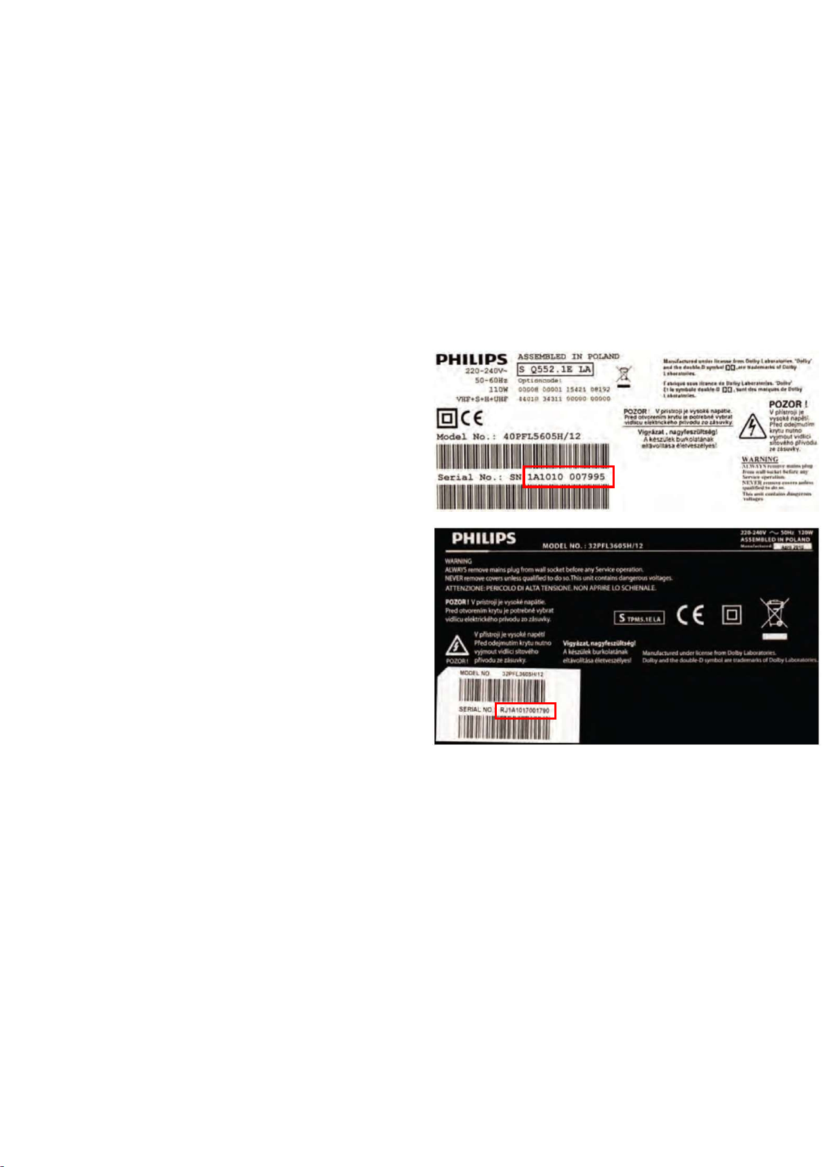
For the third digit, the numbers 1...9 and the characters
A...Z can be used, so in total: 9 plus 26= 35 different
B.O.M.s can be indicated by the third digit of the serial
number.
Identification: The bottom line of a type plate gives a
14-digit serial number. Digits 1 and 2 refer to the production
centre (e.g. SN is Lysomice, RJ is Kobierzyce), digit 3
refers to the B.O.M. code, digit 4 refers to the Service
version change code, digits 5 and 6 refer to the production
year, and digits 7 and 8 refer to production week (in
example below it is 2010 week 10 / 2010 week 17). The 6
last digits contain the serial number.
2.3.6 Alternative BOM identification
It should be noted that on the European Service website,
“Alternative BOM” is referred to as “Design variant”.
The third digit in the serial number (example:
AG2B0335000001) indicates the number of the alternative
B.O.M. (Bill Of Materials) that has been used for producing
the specific TV set. In general, it is possible that the same
TV model on the market is produced with e.g. two different
types of displays, coming from two different suppliers. This
will then result in sets which have the same CTN
(Commercial Type Number; e.g. 28PW9515/12) but which
have a different B.O.M. number.
By looking at the third digit of the serial number, one can
identify which B.O.M. is used for the TV set he is working
with. If the third digit of the serial number contains the
number “1” (example: AG1B033500001), then the TV set
has been manufactured according to B.O.M. number 1. If
the third digit is a “2” (example: AG2B0335000001), then
the set has been produced according to B.O.M. no. 2. This
is important for ordering the correct spare parts!
Figure 3-1 Serial number (example)
2.3.7 Board Level Repair (BLR) or Component Level
Repair (CLR)
If a board is defective, consult your repair procedure to
decide if the board has to be exchanged or if it should be
repaired on component level.
If your repair procedure says the board should be
exchanged completely, do not solder on the defective board.
Otherwise, it cannot be returned to the O.E.M. supplier for
back charging!
2.3.8 Practical Service Precautions
• It makes sense to avoid exposure to electrical shock.
While some sources are expected to have a possible
dangerous impact, others of quite high potential are of
limited current and are sometimes held in less regard.

• Always respect voltages. While some may not be
dangerous in themselves, they can cause unexpected
reactions that are best avoided. Before reaching into a
powered TV set, it is best to test the high voltage
insulation. It is easy to do, and is a good service
precaution.
2.4 Abbreviation List
0/6/12 SCART switch control signal on A/V board.
0 = loop through (AUX to TV),6 = play 16 :
9 format, 12 = play 4 : 3 format
DNR Digital Noise Reduction: noise reduction
feature of the set
AARA Automatic Aspect Ratio Adaptation:
algorithm that adapts aspect ratio to
remove horizontal black bars; keeps the
original aspect ratio
ACI Automatic Channel Installation: algorithm
that installs TV channels directly from a
cable network by means of a predefined
TXT page
ADC Analogue to Digital Converter
AFC Automatic Frequency Control: control
signal used to tune to the correct
frequency
AGC Automatic Gain Control: algorithm that
ontrols the video input of the feature box
AM Amplitude Modulation
AP Asia Pacific
AR Aspect Ratio: 4 by 3 or 16 by 9
ASF Auto Screen Fit: algorithm that adapts
aspect ratio to remove horizontal black
bars without discarding video information
ATSC Advanced Television Systems Committee,
the digital TV standard in the USA
ATV See Auto TV
Auto TV A hardware and software control system
that measures picture content, and adapts
image parameters in a dynamic way
AV External Audio Video
AVC Audio Video Controller
AVIP Audio Video Input Processor
B/G Monochrome TV system. Sound carrier
distance is 5.5 MHz
BDS Business Display Solutions (iTV)
BLR Board-Level Repair
BTSC Broadcast Television Standard Committee.
Multiplex FM stereo sound system,
originating from the USA and used e.g. in
LATAM and AP-NTSC countries
B-TXT Blue TeleteXT
C Centre channel (audio)
CEC Consumer Electronics Control bus: remote
control bus on HDMI connections
CL Constant Level: audio output to connect
with an external amplifier
CLR Component Level Repair
ComPair Computer aided rePair
CP Connected Planet / Copy Protection
CSM Customer Service Mode
CTI Color Transient Improvement: manipulates
steepness of chroma transients
CVBS Composite Video Blanking and
Synchronization
DAC Digital to Analogue Converter
DBE Dynamic Bass Enhancement: extra low
frequency amplification
DCM Data Communication Module. Also
referred to as System Card or Smartcard
(for iTV).
DDC See “E-DDC”
D/K Monochrome TV system. Sound carrier
distance is 6.5 MHz
DFI Dynamic Frame Insertion
DFU Directions For Use: owner's manual
DMR Digital Media Reader: card reader
DMSD Digital Multi Standard Decoding
DNM Digital Natural Motion
DRAM Dynamic RAM
DRM Digital Rights Management
DSP Digital Signal Processing
DST Dealer Service Tool: special remote control
designed for service technicians
DTCP Digital Transmission Content Protection; A
protocol for protecting digital audio/video
content that is traversing a high speed
serial bus, such as IEEE-1394
DVB-C Digital Video Broadcast - Cable
DVB-T Digital Video Broadcast - Terrestrial
DVD Digital Versatile Disc
DVI(-d) Digital Visual Interface (d= digital only)
E-DDC Enhanced Display Data Channel (VESA
standard for communication channel and
display). Using E-DDC, the video source
can read the EDID information form the
display.

EDID Extended Display Identification Data
(VESA standard)
EEPROM Electrically Erasable and Programmable
Read Only Memory
EMI Electro Magnetic Interference
EPG Electronic Program Guide
EPLD Erasable Programmable Logic Device
EU Europe
EXT EXTernal (source), entering the set by
SCART or by cinches (jacks)
FDS Full Dual Screen (same as FDW)
FDW Full Dual Window (same as FDS)
FLASH FLASH memory
FM Field Memory or Frequency Modulation
FPGA Field-Programmable Gate Array
FTV Flat TeleVision
Gb/s Giga bits per second
G-TXT Green TeleteXT
H H_sync to the module
HD High Definition
HDD Hard Disk Drive
HDCP High-bandwidth Digital Content Protection:
A “key” encoded into the HDMI/DVI signal
that prevents video data piracy. If a source
is HDCP coded and connected via
HDMI/DVI without the proper HDCP
decoding, the picture is put into a “snow
vision” mode or changed to a low
resolution. For normal content distribution
the source and the display device must be
enabled for HDCP “software key”
decoding.
HDMI High Definition Multimedia Interface
HP HeadPhone
I Monochrome TV system. Sound carrier
distance is 6.0 MHz
I2C Inter IC bus
I2D Inter IC Data bus
I2S Inter IC Sound bus
IF Intermediate Frequency
IR Infra Red
IRQ Interrupt Request
ITU-656 The ITU Radio communication Sector
(ITU-R) is a standards body subcommittee
of the International Telecommunication
Union relating to radio communication.
ITU-656 (a.k.a. SDI), is a digitized video
format used for broadcast grade video.
Uncompressed digital component or digital
composite signals can be used. The SDI
signal is self-synchronizing, uses 8 bit or
10 bit data words, and has a maximum
data rate of 270 Mbit/s, with a minimum
bandwidth of 135 MHz.
iTV Institutional TeleVision; TV sets for hotels,
hospitals etc.
LS Last Status; The settings last chosen by
the customer and read and stored in RAM
or in the NVM. They are called at start-up
of the set to configure it according to the
customer's preferences
LATAM Latin America
LCD Liquid Crystal Display
LED Light Emitting Diode
L/L' Monochrome TV system. Sound carrier
distance is 6.5 MHz. L' is Band I, L is all
bands except for Band I
LPL LG.Philips LCD (supplier)
LS Loudspeaker
LVDS Low Voltage Differential Signalling
Mbps Mega bits per second
M/N Monochrome TV system. Sound carrier
distance is 4.5 MHz
MHEG Part of a set of international standards
related to the presentation of multimedia
information, standardised by the
Multimedia and Hypermedia Experts
Group. It is commonly used as a language
to describe interactive television services
MIPS Microprocessor without Interlocked
Pipeline-Stages; A RISC-based
microprocessor
MOP Matrix Output Processor
MOSFET Metal Oxide Silicon Field Effect Transistor,
switching device
MPEG Motion Pictures Experts Group
MPIF Multi Platform InterFace
MUTE MUTE Line
MTV Mainstream TV: TV-mode with Consumer
TV features enabled (iTV)
NC Not Connected
NICAM Near Instantaneous Compounded Audio
Multiplexing. This is a digital sound system,
mainly used in Europe.
NTC Negative Temperature Coefficient,
non-linear resistor

NTSC National Television Standard Committee.
Color system mainly used in North
America and Japan. Color carrier NTSC
M/N= 3.579545 MHz, NTSC 4.43=
4.433619 MHz (this is a VCR norm, it is
not transmitted off-air)
NVM Non-Volatile Memory: IC containing TV
related data such as alignments
O/C Open Circuit
OSD On Screen Display
OAD Over the Air Download. Method of
software upgrade via RF transmission.
Upgrade software is broadcasted in TS
with TV channels.
OTC On screen display Teletext and Control;
also called Artistic (SAA5800)
P50 Project 50: communication protocol
between TV and peripherals
PAL Phase Alternating Line. Color system
mainly used in West Europe (colour carrier
= 4.433619 MHz) and South America
(colour carrier PAL M = 3.575612 MHz and
PAL N = 3.582056 MHz)
PCB Printed Circuit Board (same as “PWB”)
PCM Pulse Code Modulation
PDP Plasma Display Panel
PFC Power Factor Corrector (or
Pre-conditioner)
PIP Picture In Picture
PLL Phase Locked Loop. Used for e.g. FST
tuning systems. The customer can give
directly the desired frequency
POD Point Of Deployment: a removable CAM
module, implementing the CA system for a
host (e.g. a TV-set)
POR Power On Reset, signal to reset the uP
PSDL Power Supply for Direct view LED
backlight with 2D-dimming
PSL Power Supply with integrated LED drivers
PSLS Power Supply with integrated LED drivers
with added Scanning functionality
PTC Positive Temperature Coefficient,
non-linear resistor
PWB Printed Wiring Board (same as “PCB”)
PWM Pulse Width Modulation
QRC Quasi Resonant Converter
QTNR Quality Temporal Noise Reduction
QVCP Quality Video Composition Processor
RAM Random Access Memory
RGB Red, Green, and Blue. The primary color
signals for TV. By mixing levels of R, G,
and B, all colors (Y/C) are reproduced.
RC Remote Control
RC5 / RC6 Signal protocol from the remote control
receiver
RESET RESET signal
ROM Read Only Memory
RSDS Reduced Swing Differential Signalling data
interface
R-TXT Red TeleteXT
SAM Service Alignment Mode
S/C Short Circuit
SCART Syndicat des Constructeurs d'Appareils
Radiorécepteurs et Téléviseurs
SCL Serial Clock I2C
SCL-F CLock Signal on Fast I2C bus
SD Standard Definition
SDA Serial Data I2C
SDA-F DAta Signal on Fast I2C bus
SDI Serial Digital Interface, see “ITU-656”
SDRAM Synchronous DRAM
SECAM SEequence Couleur Avec Mémoire.
Colour system mainly used in France and
East Europe. Colour carriers = 4.406250
MHz and 4.250000 MHz
SIF Sound Intermediate Frequency
SMPS Switched Mode Power Supply
SoC System on Chip
SOG Sync On Green
SOPS Self Oscillating Power Supply
SPI Serial Peripheral Interface bus; a 4-wire
synchronous serial data link standard
S/PDIF Sony Philips Digital InterFace
SRAM Static RAM
SRP Service Reference Protocol
SSB Small Signal Board
SSC Spread Spectrum Clocking, used to
reduce the effects of EMI
STB Set Top Box
STBY STand-BY
SVGA 800 × 600 (4:3)
SVHS Super Video Home System
SW Software
SWAN Spatial temporal Weighted Averaging
Noise reduction
SXGA 1280 × 1024

TFT Thin Film Transistor
THD Total Harmonic Distortion
TMDS Transmission Minimized Differential
Signalling
TS Transport Stream
TXT TeleteXT
TXT-DW Dual Window with TeleteXT
UI User Interface
uP Microprocessor
UXGA 1600 × 1200 (4:3)
V V-sync to the module
VESA Video Electronics Standards Association
VGA 640 × 480 (4:3)
VL Variable Level out: processed audio output
toward external amplifier
VSB Vestigial Side Band; modulation method
WYSIWYR What You See Is What You Record: record
selection that follows main picture and
sound
WXGA 1280 × 768 (15:9)
XTAL Quartz crystal
XGA 1024 × 768 (4:3)
Y Luminance signal
Y/C Luminance (Y) and Chrominance (C)
signal
YPbPr Component video. Luminance and scaled
color difference signals (B-Y and R-Y)
YUV Component video
3. Mechanical Instructions
(1054)
8
J
ECN
701
ECN
401
ECN
408
701
416
01
Wifi module
W
LOUD SPERKER
ECN
601
ECN
601
ECN
415
(1054)
8
J
ECN
701 ECN
401 ECN
408
401
415CN416
01
Wifi module
W
LOUD SPERKER
ECN
601
ECN
601 ECN
415
LOUD SPERKER
LOUD SPERKER
8601
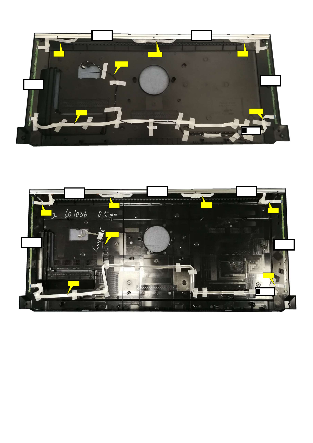
3.1 Cable Dressing
IR/LED BOARD
(1056)
MAIN POWER SUPPLY
A
(1184)
CN9102
CN
Cable dressing (50" 6233 series)
CN701
CN
CN
CN40
SSB (1053)
B
CN6
(1184)
(Wifi02)
IR/LED BOARD
(1056)
(1184)
CN8601 CN9103
MAIN POWER SUPPLY
A
(Wifi02)
Cable dressing (55" 6233 series)
CN415
CN401
CN40
CN6
CN
CN
SSB (1053)
B
(1184)
KEY BOARD
E
ECN
416
ECN02 EXA02
(1054)
CN
442
9201
9102
J
ECN
701
ECN
403 ECN
442
Wifi module
W
LOUD SPERKER
ECN
601
ECN
601
ECN
414
LOUD SPERKER
CN
441
(1
186)
ECN
441 ECN
603
ECN
9201
, ECN9202
ECN
9102
LED BOARD
ECN
701
AMBILIGHT
(1061)
AMBILIGHT
(1061)
(1057)
Back cover overview (6233 series)
MAIN POWER SUPPLY
A
IR/LED BOARD
(1056)
(1184)
CN
CN9101
for 55”
CN
for 65”
WOOFER
(1068)
Cable dressing (55/65" OLED873 series)
(Wifi02)
CN403
CN414
CN603
CN601
CN701
(1184)
CN412
B
CN1163CN1162
SSB (1053)
ECN
412
ECN02
E
XA02 E
XA02-1 E
XA04 E
XA04-1
KEY BOARD
E
AMBILIGHT
ECN03
KEY BOARD
E
ECN
412
E
XA04 E
XA04 E
XA04
E
XA02
E
XA02
(1062)
AMBILIGHT
(1062)
AMBILIGHT
(1061)
AMBILIGHT
(1062)
Back cover overview (55" OLED873 series)
AMBILIGHT
(1062)
AMBILIGHT
(1061)
(1057)
AMBILIGHT
(1062)
AMBILIGHT
(1061)
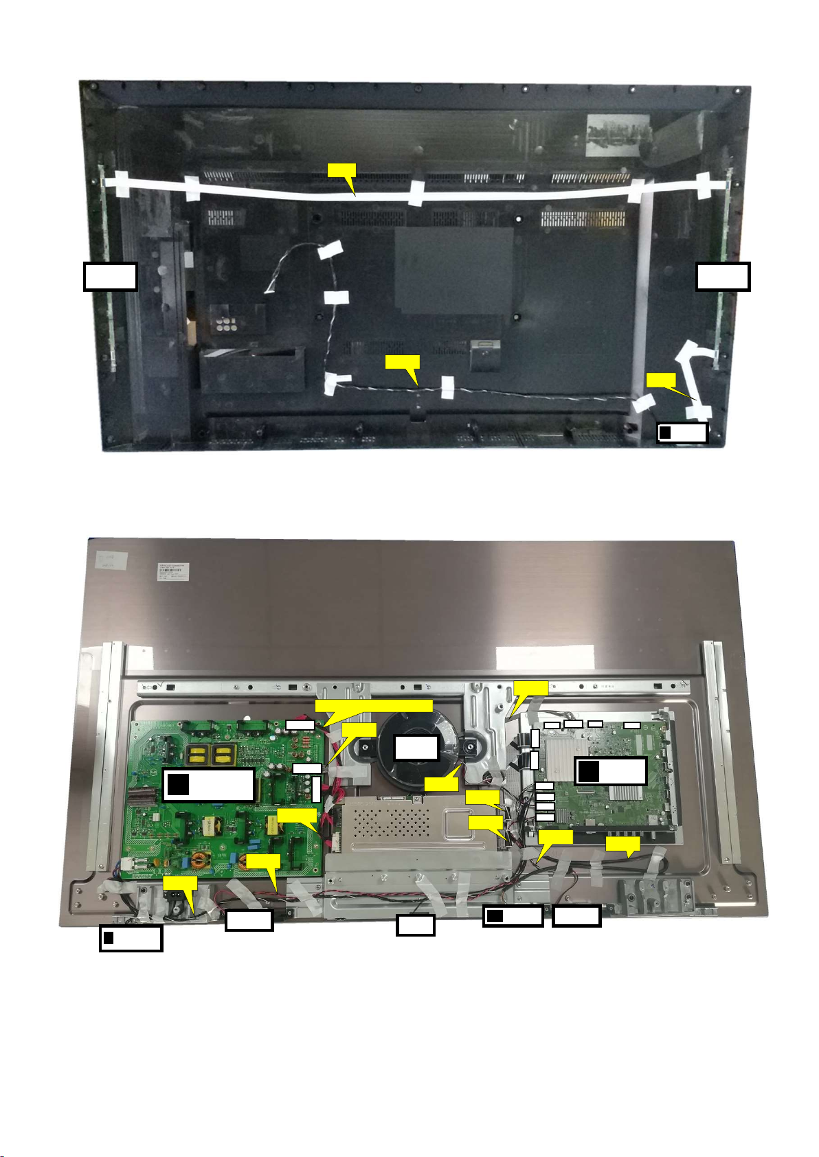
3.2 Assembly/Panel Removal
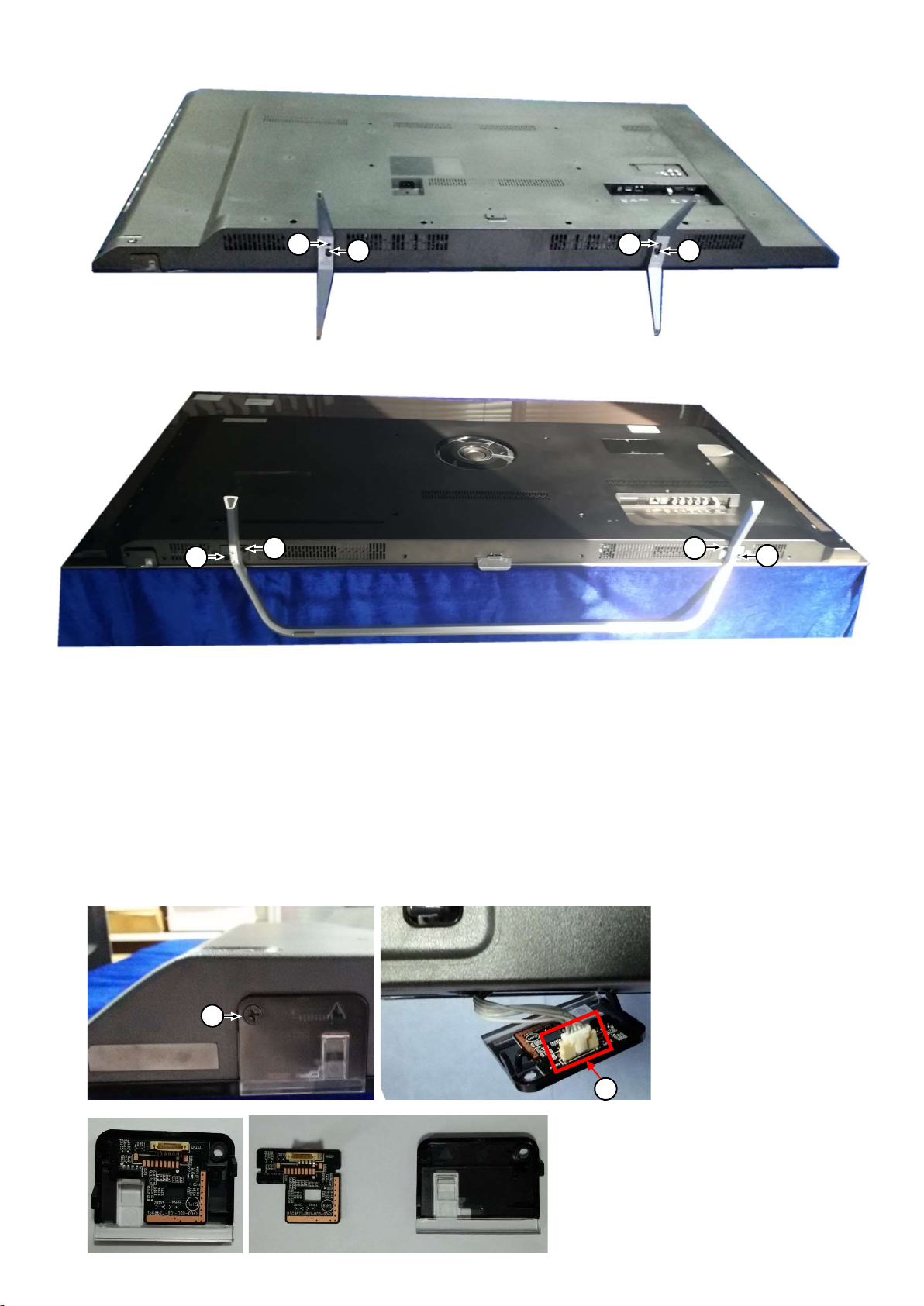
3.2.1 Stand removal
1. Remove the fixation screws [1] that secure the stand.
2. Take the stand bracket out from the set.
AMBILIGHT
(1061)
(1057)
Back cover overview (65" OLED873 series)
1 1 1
1 1
1
(50/55” 6233 series)
1
3.2.2 IR board Control Unit
1. Unplug the connector from the SSB.
Caution: be careful, as these are very fragile connectors!
2. Remove all the fixation screws [1] and connector [2] from the IR board control unit.
3. Remove the IR lens, IR board from the DECO_REAR_COVER.
When defective, replace the whole unit.
1
(55/65” OLED873 series)
1
2
2
1 1
1
3 2
3
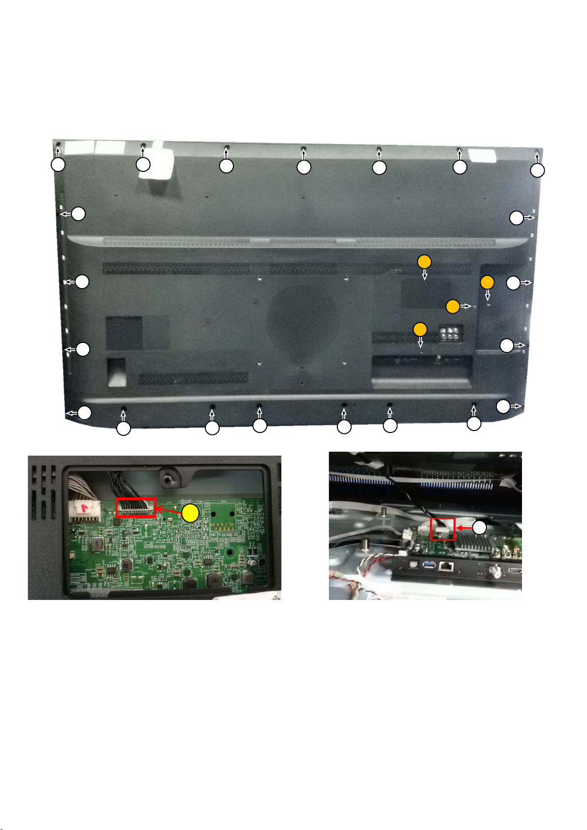
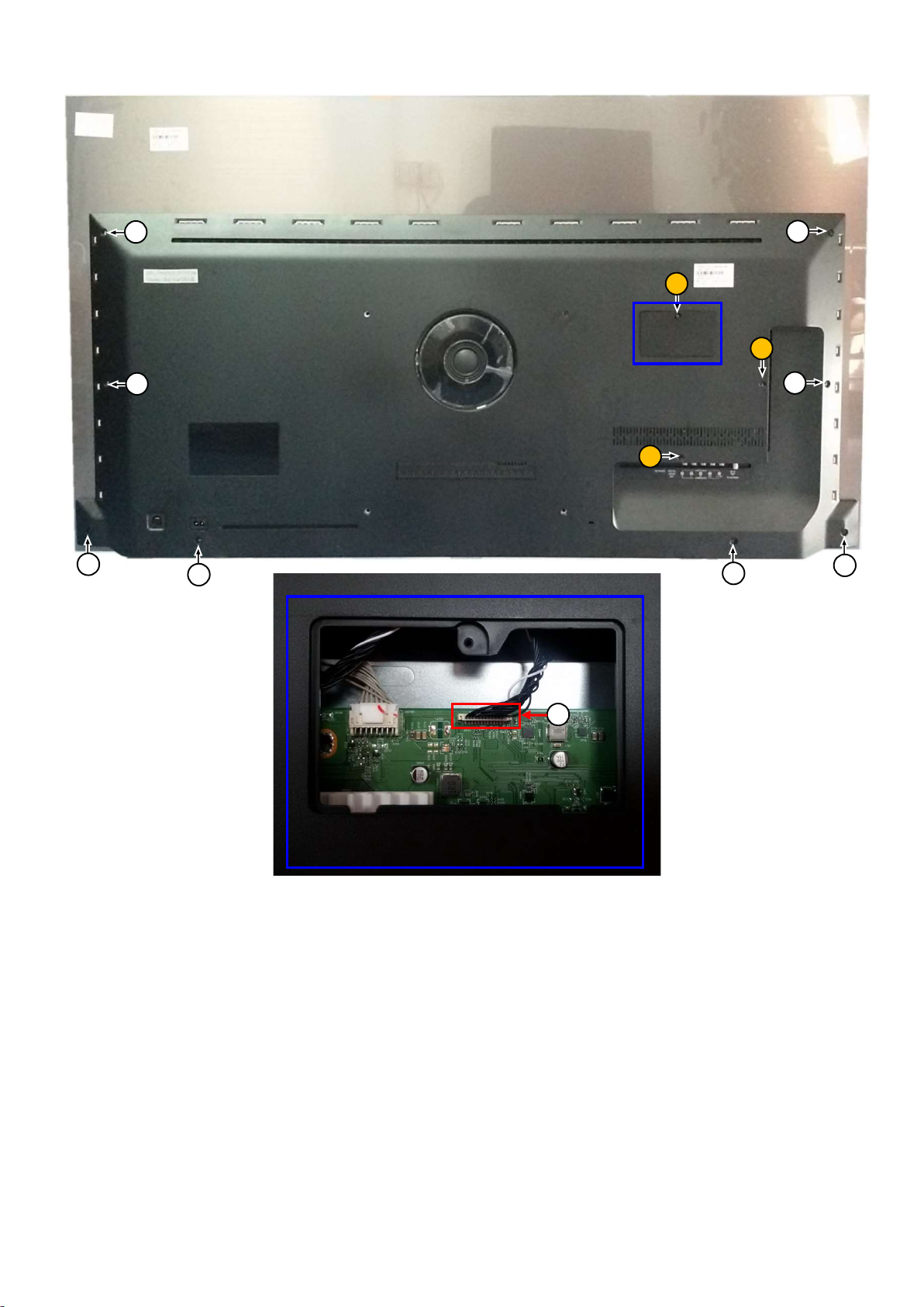
3.2.3 Rear Cover
Warning: Disconnect the mains power cord before removing the rear cover.
1. Remove fixation screws [1] and [2] that secure the rear cover.
2. Unplug connector [3] carefully.
3. Gently lift the rear cover from the TV. Make sure that wires and cables are not damaged while lifting the rear cover from the set.
1
1
1
1
1
1
1
1
2
1
2
1
1
1
1
1
1
1
1
1
(For 50” 6233 series) (For 55” 6233 series)
1
1
1
2
2
1
1
2
1
1
1
3
3.2.4 Keyboard Control Unit
Caution: be careful, the Keyboard is catch on the Back cover, please be careful to avoid damage the fragile connectors!
1. Remove all the fixation screws [1].
2. Release the connector [2] then take it out from back cover.
When defective, replace the whole unit.
(For 55/65” OLED873 series)
2
1
2
1
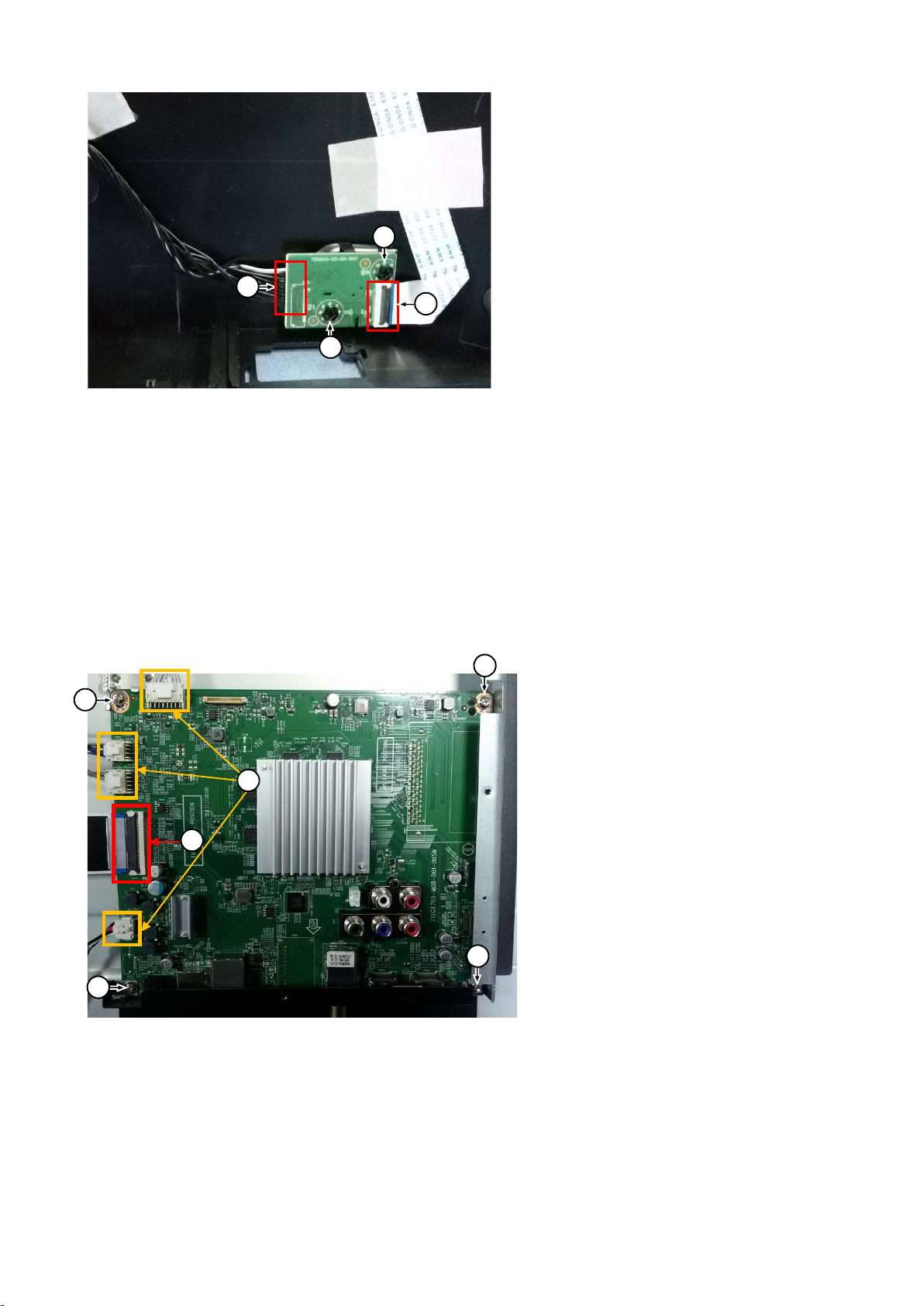
3.2.5 Small Signal Board (SSB)
Caution: it is mandatory to remount all different screws at their original position during re-assembly. Failure to do so may result in damaging the
SSB.
1. Release the clips from the LVDS connector that connect with the SSB[1].
Caution: be careful, as these are very fragile connectors!
1. Unplug all other connectors [2].
3. Remove all the fixation screws [3].
4. The SSB can now be shifted from side connector cover, then lifted and taken out of the I/O bracket.
3
1
3
3.2.6 Power Supply Unit (PSU)
3
2
3
Caution: it is mandatory to remount all different screws at their original position during re-assembly. Failure to do so may result in damaging the
PSU.
1. Gently unplug all connectors from the PSU.
2. Remove all fixation screws from the PSU.
3. The PSU can be taken out of the set now.

3.2.7 Speakers
1. Gently release the tapes that secure the speaker cables.
2. Unplug the speaker connector from the SSB.
3. Take the speakers out.
When defective, replace the both units.
3.2.8 WIFI module
1. Unplug the connector from the SSB.
2. Remove fixation screw that secure the WIFI module.
When defective, replace the whole unit.
3.2.9 LCD Panel
1. Remove the SSB as described earlier.
2. Remove the PSU as described earlier.
3. Remove the keyboard control panel as described earlier.
4. Remove the stand bracket as described earlier.
5. Remove the IR/LED as described earlier.
6. Remove the fixations screws that fix the metal clamps to the front bezel. Take out those clamps.
7. Remove all other metal parts not belonging to the panel.
8. Lift the LCD Panel from the bezel.
When defective, replace the whole unit.

4. Service Modes
4.1 Service Modes
The Service Mode feature is split into following parts:
Service Alignment Mode (SAM).
Factory Mode.
Customer Service Mode (CSM).SAM and the Factory mode offer features, which can be used by the Service engineer to repair/align a TV set.
SAM and the Factory mode offer features, which can be used by the Service engineer to repair/align a TV set. Some features are:
Make alignments (e.g. White Tone), reset the error buffer (SAM and Factory Mode).
Display information (“SAM” indication in upper right corner of screen, error buffer, software version, operating hours,options and option codes,
sub menus).
The CSM is a Service Mode that can be enabled by the consumer. The CSM displays diagnosis information, which the customer can forward to the
dealer or call centre. In CSM mode, “CSM”, is displayed in the top right corner of the screen. The information provided in CSM and the purpose of
CSM is to:
Increase the home repair hit rate.
Decrease the number of nuisance calls.
Solved customers’ problem without home visit.
Note: For the new model range, a new remote control (RC) is used with some renamed buttons. This has an impact on the activation of the Service
modes. For instance the old “MENU” button is now called “HOME” (or is indicated by a “house” icon).
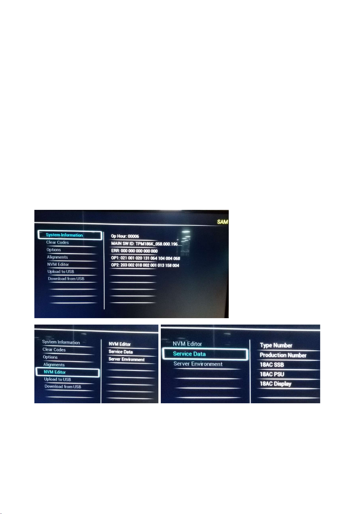
4.2 Service Alignment Mode (SAM)
Purpose
To modify the NVM.
To display/clear the error code buffer.
To perform alignments.
Specifications
Operation hours counter (maximum five digits displayed).
Software version, error codes, and option settings display.
Error buffer clearing.
Option settings.
Software alignments (White Tone).
NVM Editor.
Set screen mode to full screen (all content is visible).
How to Activate SAM
To activate SAM, use one of the following methods:
Press the following key sequence on the remote control transmitter: “062596”, directly followed by the “INFO/OK” button. Do not allow the
display to time out between entries while keying the sequence.
Or via ComPair.
After entering SAM, the following items are displayed,
with “SAM” in the upper right corner of the screen to indicate that the television is in Service Alignment Mode.
How to Navigate
In the SAM menu, select menu items with the UP/DOWN keys on the remote control transmitter. The selected item will be indicated. When not
all menu items fit on the screen, use the UP/DOWN keys to display the next/previous menu items.
With the “LEFT/RIGHT” keys, it is possible to:
– (De) activate the selected menu item.
– (De) activate the selected sub menu.
– Change the value of the selected menu item.
When you press the MENU button once while in top level SAM, the set will switch to the normal user menu (with the SAM mode still active in the
background).
How to Store SAM Settings
To store the settings changed in SAM mode (except the RGB Align settings), leave the top level SAM menu by using the POWER button on the
remote control transmitter or the television set. The mentioned exceptions must be stored separately via the STORE button.
How to Exit SAM
Use one of the following methods:
Switch the set to STANDBY by pressing the mains button on the remote control transmitter or the television set.
Via a standard RC-transmitter, key in “00” sequence.
Note: When the TV is switched “off” by a power interrupt while in SAM, the TV will show up in “normal operation mode” as soon as the power is
supplied again. The error buffer will not be cleared.
SAM mode overview
Remark: Under main menu “NVM editor”,choose “Service Data”, you can use the UP/DOWN keys to view and change the set Type number, the
set Production Number or the 18AC of a part.(The NVM-editor still has the same function as before, alpha-numeric entry.)
4.3 Factory mode:
Purpose
To perform extended alignments.
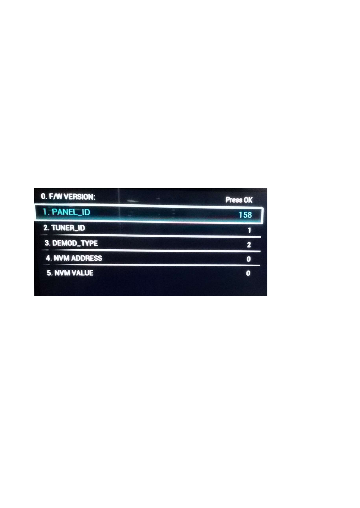
Specifications
Displaying and or changing Panel ID information.
Displaying and or changing Tuner ID information.
Error buffer clearing.
Various software alignment settings.
Testpattern displaying.
Public Broadcasting Service password Reset.
etc.
How to Activate the Factory mode
To activate the Factory mode, use the following method:
Press the following key sequence on the remote control transmitter: from the “menu/home” press “1999”, directly followed by the
“Back/Return” button. Do not allow the display to time out between entries while keying the sequence.
After entering the Factory mode, we can see many items displayed, use the UP/DOWN keys to display the next/previous menu items
Factory mode overview
How to Exit the Factory mode
Use one of the following methods:
Select EXIT_FACTORY from the menu and press the “OK” button.
Note: When the TV is switched “off” by a power interrupt, or normal switch to “stand-by” while in the factory mode, the TV will show up in “normal
operation mode” as soon as the power is supplied again. The error buffer will not be cleared.
4.4 Customer Service Mode (CSM)
Purpose
The Customer Service Mode shows error codes and information on the TVs operation settings.The call centre can instruct the customer (by
telephone) to enter CSM in order to identify the status of the set.This helps the call centre to diagnose problems and failures in the TV set before
making a service call.
The CSM is a read-only mode; therefore, modifications are not possible in this mode.
Specifications
Ignore “Service unfriendly modes”.
Line number for every
line (to make CSM language independent).
Set the screen mode to full
screen (all contents on screen is visible).
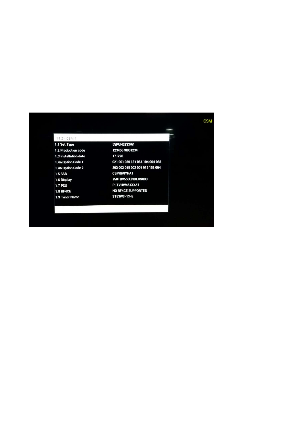
After leaving the Customer Service Mode, the original settings are restored.
Possibility to use “CH+” or “CH-” for channel surfing, or enter the specific channel number on the RC.
How to Activate CSM
To activate CSM, press the following key sequence on a standard remote control transmitter: “123654” (do not allow the display to time out
between entries while keying the sequence). After entering the Customer Service Mode, the following items are displayed. use the Right/Left keys
to display the next/previous menu items
Note: Activation of the CSM is only possible if there is no (user) menu on the screen!
CSM Overview
How to Navigate
By means of the “CURSOR-DOWN/UP” knob (or the scroll wheel) on the RC-transmitter, can be navigated through the menus.
How to Exit CSM
To exit CSM, use one of the following methods.
Press the MENU/HOME button on the remote control transmitter.
Press the POWER button on the remote control transmitter.
Press the POWER button on the television set.
5. Software Upgrading, Error code and Panel Code
5.1 Software Upgrading
5.1.1. The following update is for .pkg file.
1. Rename the file to “upgrade_loader.pkg”.
2. Prepare a USB memory (File format: FLAT, Size: 1G~8G).
3. Copy the software to USB flash disk (root directory).
4. Switch off the TV and Insert the USB memory stick that contains the software update files in one of the TV’s USB 2.0 port.
Note: It contains USB3.0 port, if connect on it, the software may can’t be detected.
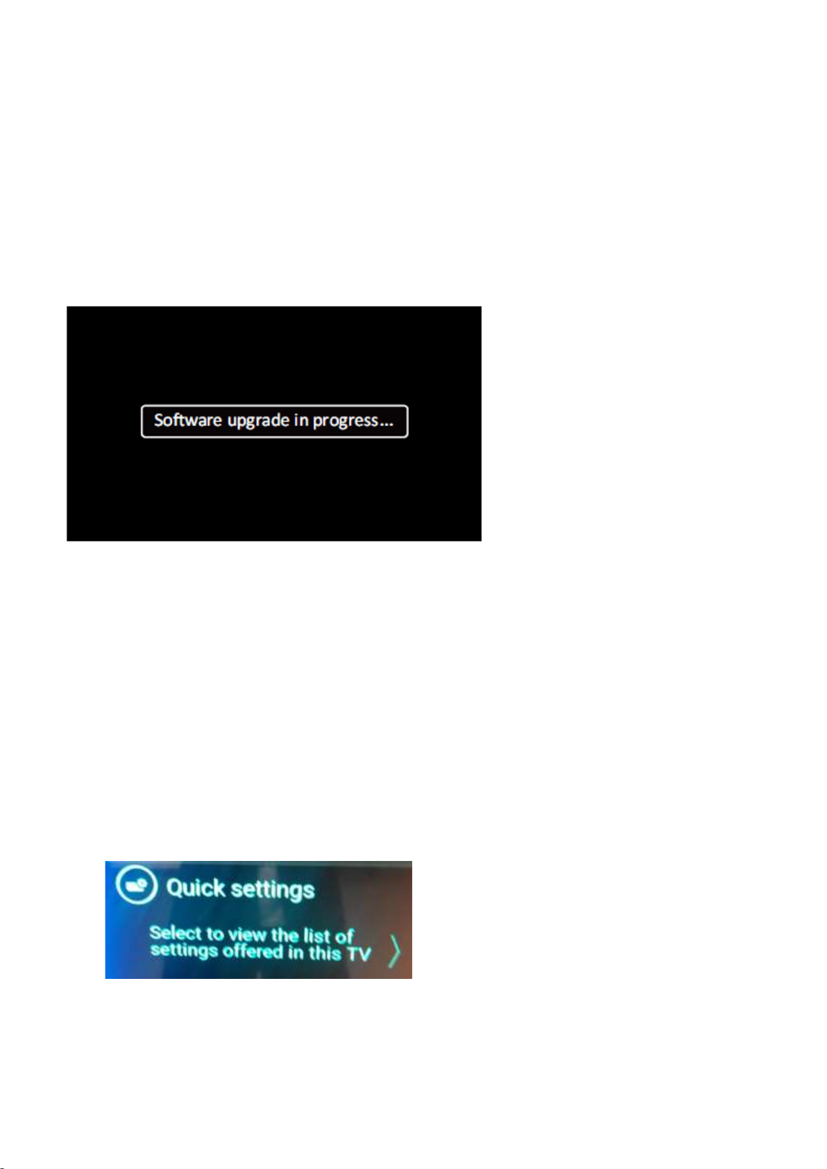
5. Switch on the TV. The TV will detect the USB memory stick automatically. Then a window jumps out as below
6. When the TV software is updated, the TV will turn on again automatically. Remove your USB flash drive.
7. We can enter in CSM or Factory mode to check the current software version.
5.1.2. The following update is for .upg file.
Step 1: Ready for F/W Upgrade
1. Rename the file to “autorun.upg”.
2. Prepare a USB memory (File format: FLAT, Size: 1G~8G).
3. Copy the software to USB flash disk (root directory).
4. Switch on the TV and Insert the USB memory stick that contains the software update files in one of the TV’s USB 2.0 port.
Note the version of this F/W before you change the software file name.
Step 2: F/W Upgrade
1. Press [Quick settings], then Choose [Update Software] in the Settings menu
2. Choose [Local Updates], then press OK.

3. Select the file that you downloaded and press OK
4. Choose [Update], then choose [Start] on following step
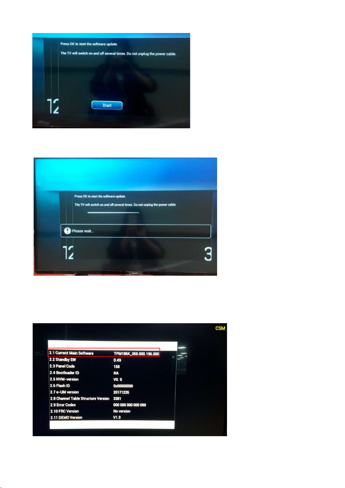
5. Upgrade in progress
Step 3: Check the SW version.
1. After burning software, TV will restart
2. Press “123654”, enter Customer Service Mode to check if the software version is correct.
Caution: Please make sure that software upgrade is finished before unplug the USB and AC power!

5.2 Error Code
5.2.1 Introduction
Error codes are required to indicate failures in the TV set. In principle a unique error code is available for every:
• Activated (SW) protection.
• Failing I2C device.
• General I2C error.
The last five errors, stored in the NVM, are shown in the Service menu’s. This is called the error buffer.
The error code buffer contains all errors detected since the last time the buffer was erased. The buffer is written from left to right. When an error occurs that
is not yet in the error code buffer, it is displayed at the left side and all other errors shift one position to the right.
An error will be added to the buffer if this error differs from any error in the buffer. The last found error is displayed on the left.
An error with a designated error code never leads to a deadlock situation. It must always be diagnosable (e.g. error buffer via OSD or blinking LED).
In case a failure identified by an error code automatically results in other error codes (cause and effect), only the error code of the MAIN failure is displayed.
5.2.2 How to Read the Error Buffer
You can read the error buffer in three ways:
• On screen via the SAM/CSM (if you have a picture).
Example:
– ERROR: 000 000 000 000 000: No errors detected
– ERROR: 013 000 000 000 000: Error code 13 is the last and only detected error
– ERROR: 034 013 000 000 000: Error code 13 was detected first and error code 34 is the last detected (newest) error
• Via the blinking LED procedure (when you have no picture).
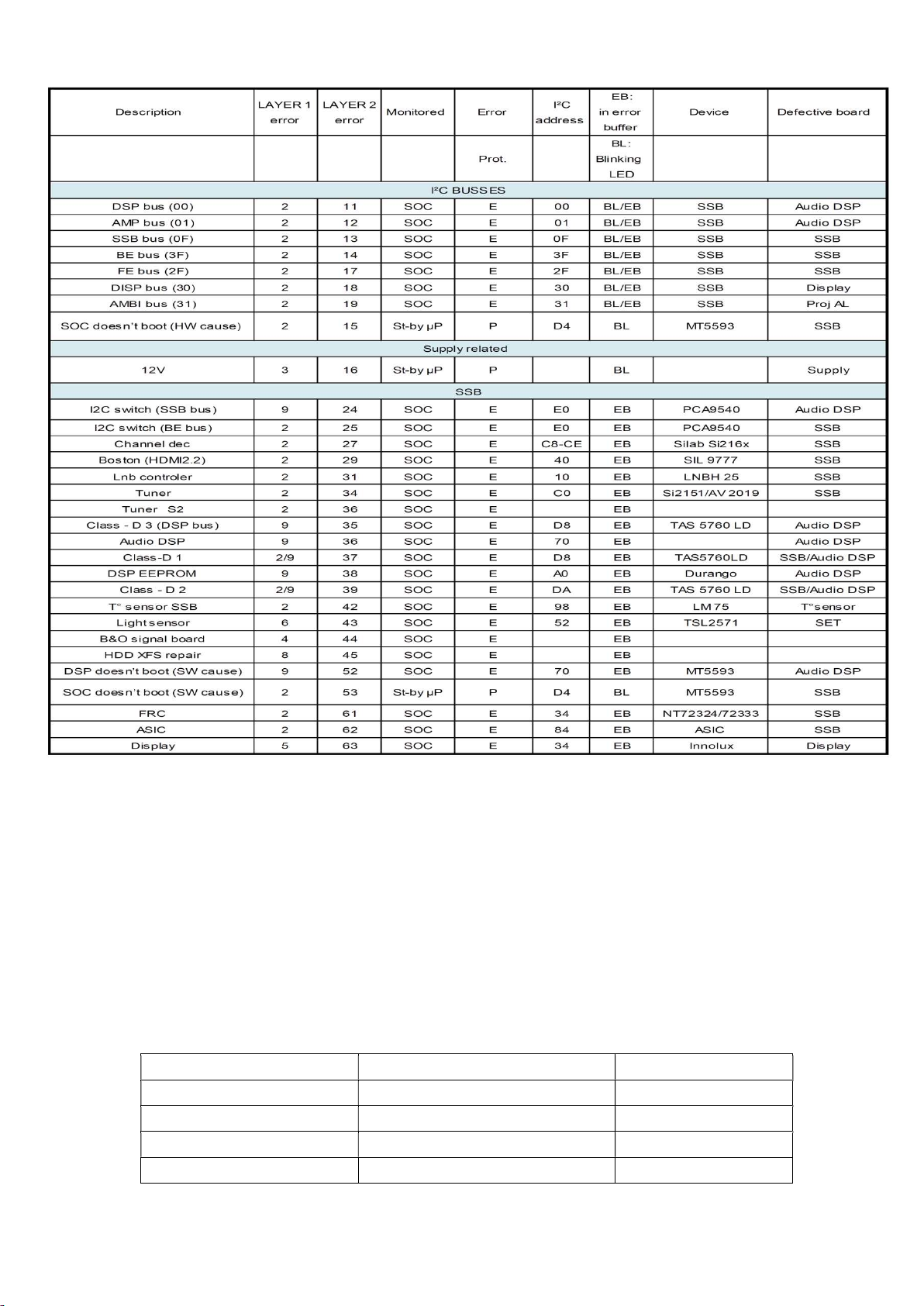
5.2.3 Error codes overview
In this chassis only “layer 2” error codes are available and point to problems on the SSB. They are triggered by LED blinking
when CSM is activated. Only the following layer 2 errors are defined:
5.2.4 How to Clear the Error Buffer
The error code buffer is cleared in the following cases:
• By using the CLEAR command in the SAM menu
• By using the CLEAR command in the Factory mode:
• By using the following key sequence on the remote control transmitter: “062599” directly followed by the OK button.
• If the contents of the error buffer have not changed for 50 hours, the error buffer resets automatically.
Note: If you exit SAM by disconnecting the mains from the television set, the error buffer is not reset.
5.3 Panel Code
Press the following key sequence on a standard RC transmitter: “062598” directly followed by MENU and “xxx”, where “xxx” is a 3 digit decimal value
of the panel type: see column “Display Code” in below tab. After resetting the Display Code, restart the set immediately.
CTN_ALT BOM# Panel Type Display Code
50PUN6233/61 TPT500U1-QVN03.U S7B0AA 153
55PUN6233/61 TPT550J1-QUBN40.K SD850E 158
55OLED873/61 LC550AQD-GJAB 161
65OLED873/61 LC650AQD-EKAA 162
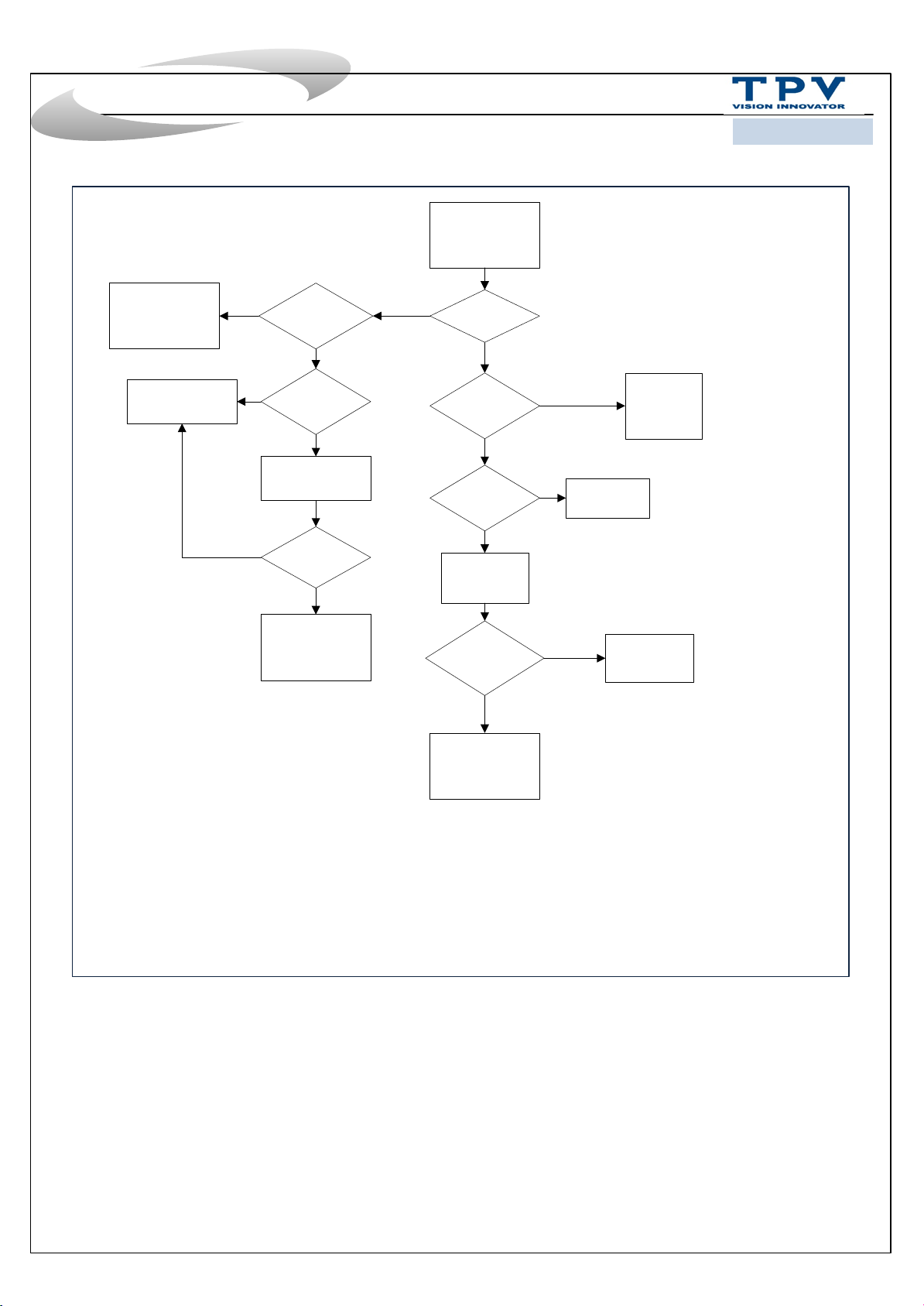
Trouble shooting
Picture-related
2016年12月10日
2016/4/8
Ask Photo
SW
issue
N
Intermittent
problem ?
Y
Y
SW latest ?
N
Update SW
N
Problem
solved ?
Y
Finish
Y
Picture ?
N
Backlight?
N
LED working ?
Y
Sound ?
SW+SSB
Y
N
PSU/SSB
Y
PSU+ Panel
Menu Smarkt
function?
N
SSB+LVDS+Panel
RAM
Y
Signal
issue
Trouble shooting
Audio/Sound-
related
2016年12月10日
2016/4/8
HW
issue
SW
N
Intermittent
problem ?
Y
Y
SW latest ?
N
Update SW
N
Problem
solved ?
Y
Finish
Y
Sound ?
N
Mute ?
N
Extra device
connect?
N
Factory
setting
Sound back ? Setting issue
N
Y
Y
Check extra
Y
device
Setting
issue
SSB+SPK
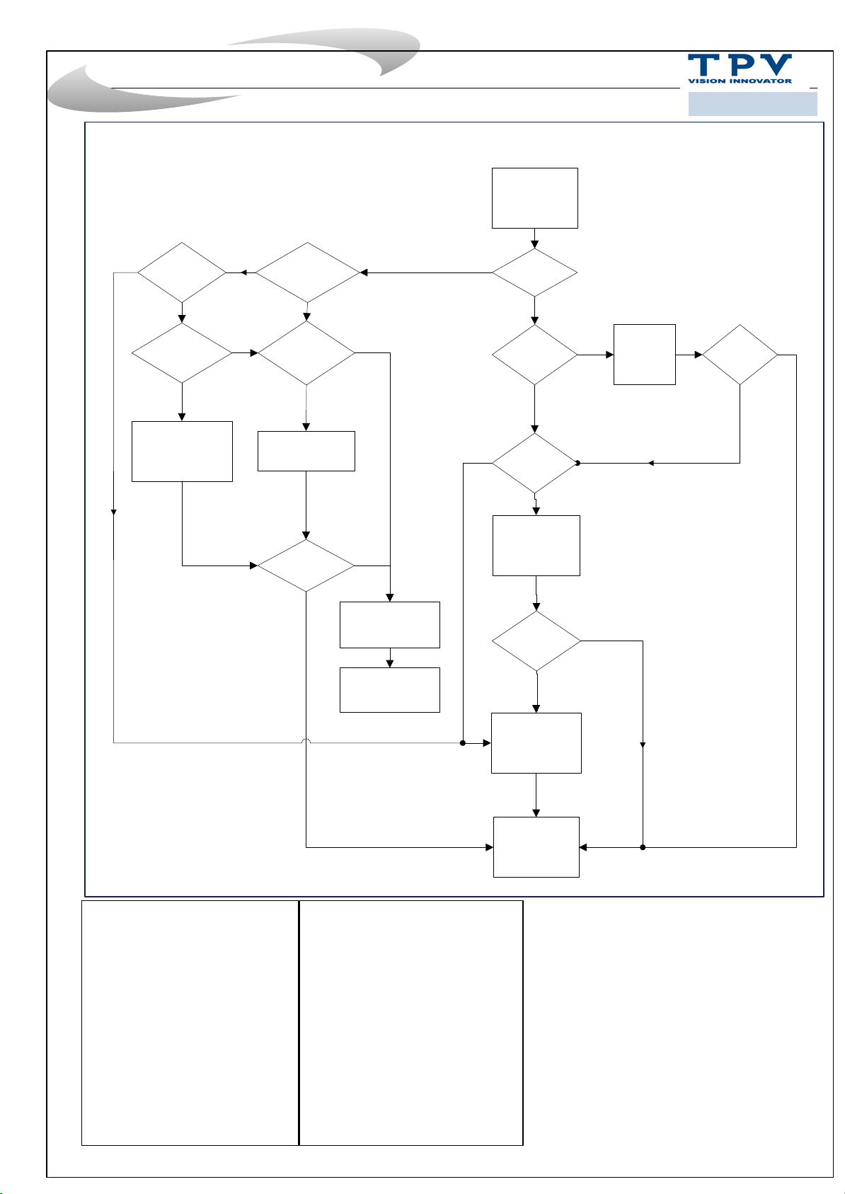
Trouble shooting system
N
Smart
function
issue ?
N
Intermittent
problem ?
Remark2:
Y
Y
2016年4月11日
2016/12/11
System related
Remark1:
Y
TV start
up ?
N
Network
connect ?
N
Connect network
Y
SW latest ?
N
Update SW
Problem
solved ?
Y
Y
N
SW issue
Commerce way
SCC
available ?
Y
Execute
SCC
Problem
solved ?
Y
N
N
SW update
available ?
Y
SW update
N
Problem
Y
solved ?
N
HW repair
Remark1 : What is System related issue ?
1.Permanent reboots
2.Intermittent reboots
3.No function, no standby LED (set dead)
4.No function, blinking LED
5.Set freezes, intermittently
6.Slow response to user interaction
7.Switches ON by itself
8.Switches Off by itself
9.Stuck in standby mode / unable to start up
10.Stuck on PHILIPS / ANDROID logo
11.CAM not recognized by TV
12.CAM authentication issue
13.Misc CAM issue
14.IP-EPG issues
15.BC-EPG issues
16.PVR issues w/ BC-EPG
17.PVR issues w/ IP-EPG
18.PVR issues / generic
19.EDFU-related issue
20.Features not available in UI / cannot be activated
Remark2 : How to judge intermittent issue ?
1.When the problem happened can be solved by:
1)AC off AC on
2)DC off DC on
3)RC switch different source
2.The problem intermittent happened
Finish

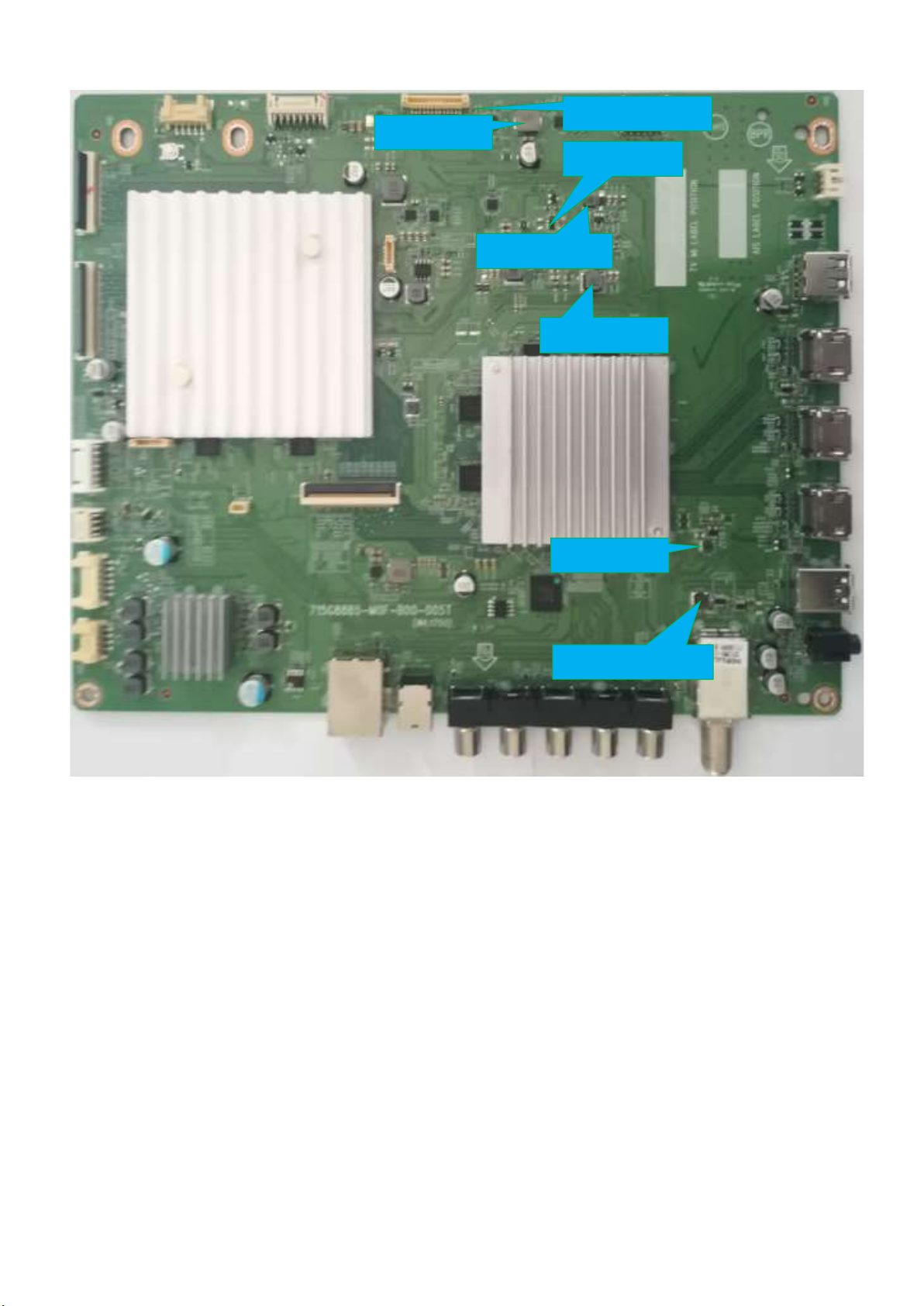
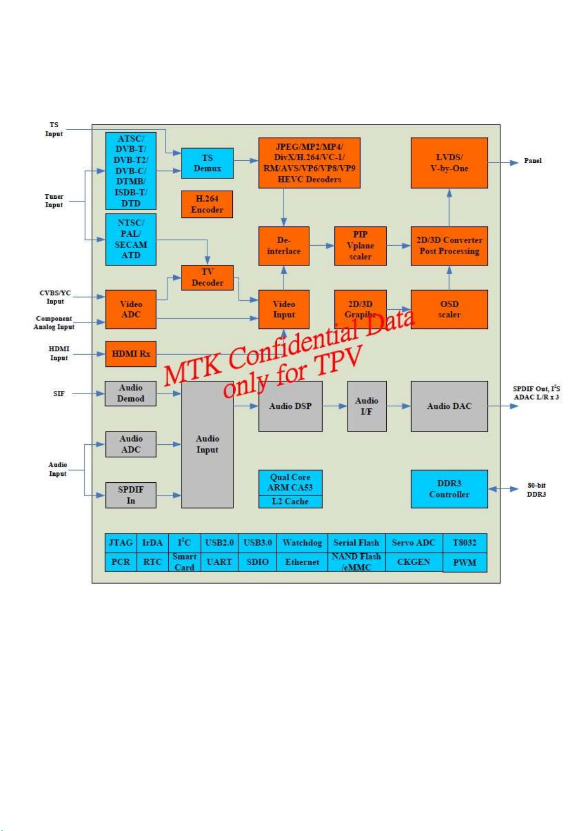
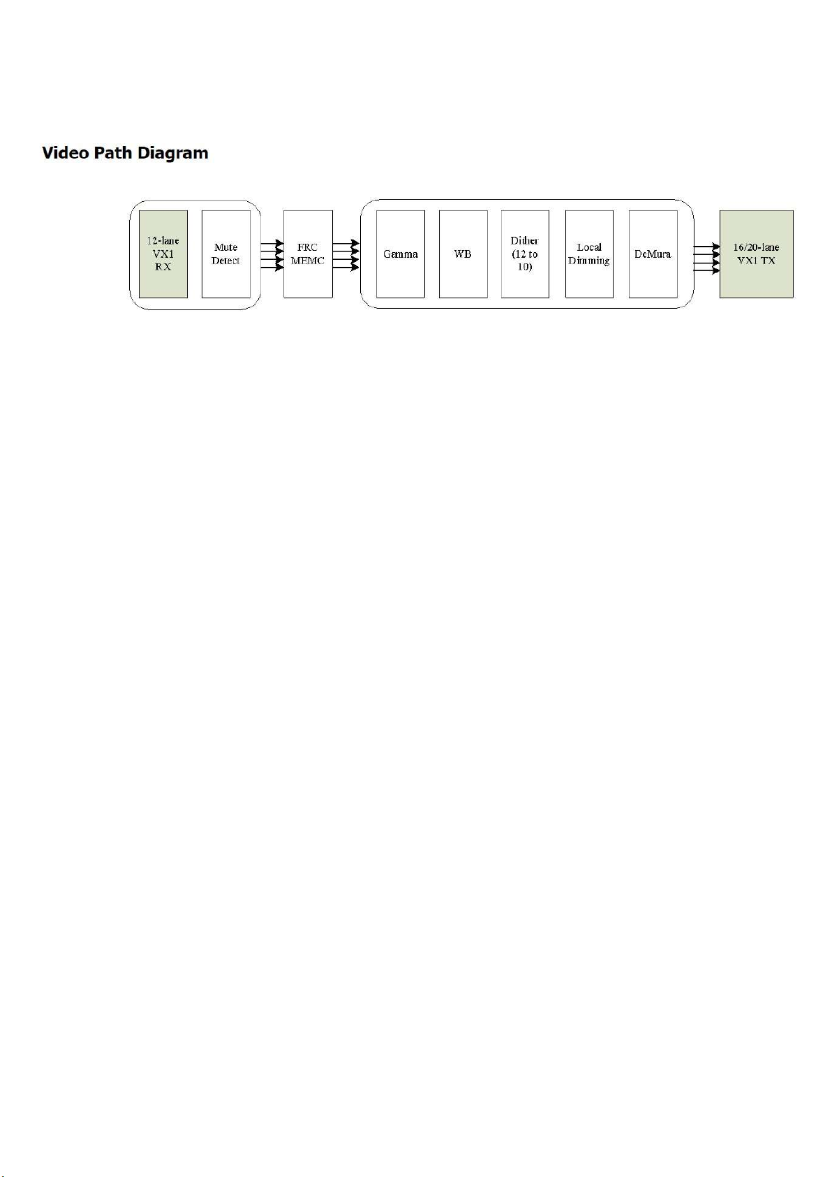
7. Electrical Diagram
7.1 Block diagram
(For 715G8709M)
(For 715G8885M)

7.2 Power Supply
CN701
12V
AUDIO
AMP
DIM
Main filter
Power architecture of this platform.
LVDS
12V
7.3 Power tree
Display power
CN8601
CN9102&CN9201 For
715G8886P
PFC
Platform power
ON/OFF
PS_ON
12V
12V_A
AC-input +
AC IN
Platform
MT5802
(For 715G8709M)

POWER TREE
AU_12 V
FB601
AUDIO AMP
PVDD
AD875 88
R8058
BUCK CONVERTER
SY836 6QNC
U701
OPWRSB_PWR
BUCK CONVERTER
SY836 6QNC
U708
BUCK CONVERTER
SY836 6QNC
U706
+18V
BUCK CONVERTER
SY823 4FCC
U713
OPWRSB_PWR
R783
R782
FB707FB705
18V_1 2VMain_ 18V_1 2V
+5V_S TB
VCCK
+5V_U SB
USB 2 .0 * 2
USB 3 .0 * 1
BUCK CONVERTER
SY808 9AAAC
U707
R781
POWER SWITCH
AON4421
Q706
VCCK
R705
3V3SB
STB_P WR
(For 715G8885M)
+5V_S W
BUCK CONVERTER
SY836 6QNC
U709
FB706
POWER MOS
AO3401A
Q701
DDR_PWR_EN
R716
R717
R760
BUCK CONVERTER
RT807 9ZQW
U705
DVDD3 V3
AVDD3 V3
VCC3. 3V_FR C
FB701
FB711
DDRV
1.5V
LDO CONVERTER
G9661
U704
LDO CONVERTER
G9141
U709
R726
AVDD1 V2
VCC1. 8V_FR C
LDO_P WR

7.4 Power layout SSB
C789 +12V PANEL
L704 +3.3V SB
L701 +1.5V DDR
L702 +5V_STB
Power SSB Top View (For 715G8709M)
L803 +5V

C105 TUNER_3.3V
R221 TUNER_LNB
R726 +1.8V EMMC
Power SSB Bottom View (For 715G8709M)
L702 +5V_STB
C4458 +12V_AMBI
Q706 +5V_SW
L704 +3.3V_SB
L803 +5V_USB
L710 +1V_STB
L4102 +3.3V_TUNER
Power SSB Top View (For 715G8885M)
8. IC Data Sheets
8.1 MT5802KHEJ (IC U401--SCALER)

8.2 NT72334TBG/BA (IC U5000--SCALER)

1 2 3 4 5 6 7 8 9 10
11
12
13
14
15
16
17
18
19
20
21
22
23
24
25
26
27
28
29
30
31
32
A
mTXB0P
mTXB1N
mTXB3N
mTXB3P
mTXC0P
mTXC1N
mTXC3N
mTXC3P
mTXD0P
mTXD1N
mTXD3N
mTXD3P
mTXE0P
mTXE1N_V
TX0N
mTXE3N_V
TX3N
mTXE3P_VT
X3P
mTXF0P
mTXF1N_VT
X5N
mTXF3N_VT
X8N
mTXF3P_VT
X8P
A
B
mTXA5P
mTXB0N
mTXB1P
mTXBCKP
mTXB4N
mTXC0N
mTXC1P
mTXCCKP
mTXC4N
mTXD0N
mTXD1P
mTXDCKP
mTXD4N
mTXE0N
mTXE1P_V
TX0P
mTXECKP_
VTX2P
mTXE4N_V
TX4N
mTXF0N
mTXF1P_VT
X5P
mTXFCKP_
VTX7P
mTXF4N_V
TX9N
B
C
mTXA5N
mTXA4P
mTXB2N
mTXB2P
mTXBCKN
mTXB4P
mTXB5N
mTXB5P
mTXC2N
mTXC2P
mTXCCKN
mTXC4P
mTXC5N
mTXC5P
mTXD2N
mTXD2P
mTXDCKN
mTXD4P
mTXD5N
mTXD5P
mTXE2N_V
TX1N
mTXE2P_VT
X1P
mTXECKN_
VTX2N
mTXE4P_VT
X4P
mTXE5N
mTXE5P
mTXF2N_VT
X6N
mTXF2P_VT
X6P
mTXFCKN_
VTX7N
mTXF4P_VT
X9P
mTXF5N
mTXF5P
C
D
mTXA4N
GND_VTX
GND_VTX
GND_VTX
GND_VTX
GND_VTX
GND_VTX
GND_VTX
GND_VTX
GND_VTX
GND_VTX
GND_VTX
GND_VTX
GND_VTX
GND_VTX
GND_VTX
GND_VTX
GND_VTX
TEST_OUT
mTXG1N_V
TX10N
mTXG0P
mTXG0N
D
E
mTXACKP
mTXA3N
mTXA3P
GND_VTX
GND_VTX
GND_VTX
GND_VTX
GND_VTX
GND_VTX
GND_VTX
GND_VTX
GND_VTX
GND_VTX
GND_VTX
GND_VTX
GND_VTX
GND_VTX
GPIOB17
GPIOB16
GPIOB15
GND_VTX
mTXG1P_V
TX10P
E
F
mTXACKN
mTXA2P
mTXA2N
GND_VTX
GND_VTX
GND_VTX
GND_VTX
GPIOC08
GND_VTX
GND
GND_VTX
GND_VTX
GND_VTX
GND_VTX
GND_VTX
GND_VTX
GND_VTX
GND_VTX
GND_VTX
GND_VTX
GPIOB18
GND_VTX
mTXG2N_V
TX11N
mTXG2P_V
TX11P
mTXGCKN_
VTX12N
F
G
mTXA1P
GND_VTX
GPIOC12
GPIOC15
GND_VTX
GND
GND
GND_VTX
GND_VTX
GND_VTX
GND_VTX
GND_VTX
GND_VTX
GND_VTX
GND_VTX
GPIOB19
GPIOB20
GPIOB21
GND_VTX
mTXG3P_V
TX13P
mTXG3N_V
TX13N
mTXGCKP_
VTX12P
G
H
mTXA0N
mTXA0P
mTXA1N
GPIOC10
GPIOC14
GPIOC09
GPIOC07
GPIOC06
VTXLOCK
GND
GND
GND_VTX
GND_VTX
GND_VTX
GND_VTX
GND_VTX
GND_VTX
GND_VTX
GPIOB24
GPIOB23
GPIOB22
GND_VTX
mTXG4N_V
TX14N
H
J
GPIOC13
GPIOC11
GPIOC16
VDD_IO
VTXHTP
EXT_SWIN
G
GND
GND_VTX
GND_VTX
GND_VTX
GND_VTX
VTERM
GND_VTX
GPIOB25
GND_VTX
mTXG4P_V
TX14P
mTXG5N
mTXG5P
J
K
VTX_25V
VTX_25V
VTERM
VTERM
VTERM
GPIOB26
GPIOB27
GPIOB28
GND_VTX
mTXH1N_V
TX15N
mTXH0P
mTXH0N
K
L
GND
GND
VTX_25V
VTX_25V
VTX_25V
VTERM
VTERM
GPIOB31
GPIOB30
GPIOB29
GND_VTX
mTXH1P_V
TX15P
L
M
GND
GND
GND
GND
GND
VTX_25V
VTX_25V
VTX_25V
VTERM
VTERM
GPIOA20
GND_VTX
mTXH2N_V
TX16N
mTXH2P_V
TX16P
mTXHCKN_
VTX17N
M
N
GND
GND
GND
GND
GND
GND
GND
GND_VTX
GND_VTX
GND_VTX
GND_VTX
GPIOA19
GPIOA22
GPIOA21
GND_VTX
mTXH3P_V
TX18P
mTXH3N_V
TX18N
mTXHCKP_
VTX17P
N
P
GND
GND
GND
GND
GND
GND
GND
VDD25_DLL
_M
VCORE
VCORE
VCORE
VCORE
GND
GND
GND
VDD_IO
VDD_IO
RESETN
GND_VTX
mTXH4N_V
TX19N
P
R
A_VREFCA
A_VREFDQ
GND
GND
GND
GND
GND_DDR_
APLL_M
VDDA_MMU
_M
VDDA_MMU
_M
VCORE
VCORE
VCORE
GND
VDDQ_18
GND
GPIOB07
GND_VTX
mTXH4P_V
TX19P
mTXH5N
mTXH5P
R
T
A_ZQ
GND
GND
GND
GND
GND
GND_CLK_
M
VDD15_CLK
_M
VDD15_LD
O_M
VDD15_LDO
_M
VCORE
VCORE
GND
GND
GND
GNDA_MPLL VDD15_MP
LL
GPIOB10
GPIOB01
GPIOB02
GND
XO
XI
GND
T
U
GND
GND
VDD_DDR
VDD_DDR
GND
GND
GND
VDD_MMU_M VDD_MMU_
M
VCORE
VCORE
GND
GND
GNDA_MPLL VCCA_3V3_
MPLL
GPIOA24
GPIOA23
GPIOB08
GND
GND
U
V
VDD_DDR
VDD_DDR
VDD_DDR
VDD_DDR
VDD_DDR
VDD_DDR
VDD_DDR
VDD_MMU_M VDD_MMU_
M
VCORE
VCORE
GND
GND
VCORE
VCORE
GPIOA25
GND
GPIOA09
GPIOA08
GPIOA07
V
W
VDD_DDR
VDD_DDR
VDD_DDR
VDD_DDR
VDD_DDR
VDD_MMU_M VDD_MMU_
M
VCORE
GND
GND
VCORE
GPIOA26
GPIOA04
GPIOA05
GND
GPIOA10
W
Y
GND
GND
GND
GND
GND
GND
VCCA_DDR
_M
VDD_MMU_
M
VCORE
VCORE
GND
VRX09V
VCORE
VCORE
GPIOA31
GPIOA30
GPIOA06
GND
GPIOA11
GPIOA18
GPIOA16
Y
AA
GND
GND
GND
GND
GND
GND
GND
VCCA_DDR
_S
GND
GND
GND
GND
VRX09V
VRX_GND
GPIOA13
GND
GPIOB06
GPIOB05
GPIOA17
AA
AB
B_VREFCA
B_VREFDQ
GND
GND
GND
GND
GND
GND
GND
VRX_25V
VRX_GND
GPIOB12
GPIOA15
GPIOA14
GND
GPIOB00
AB
AC
B_ZQ
MLDO_OUT
GND
GND
GND
GND
GND
GND
VDD25_DLL
_S
VDD15_LD
O_S
VDDA_MMU
_S
VDD_MMU_
S
VDD_MMU_S VDD_MMU_S VDD_MMU_
S
VRX_25V
VRX_GND
GPIOB11
GPIOB04
GPIOB03
GND
GPIOA27
GPIOA28
GPIOA29
AC
AD
GND
GND
GND
GND
GND
GND
GND
GND
VDD15_LDO
_S
VDDA_MMU
_S
GND_CLK_S VDD_MMU_S VDD_MMU_S VDD_MMU_
S
GND
VRX_25V
VRX_GND
GPIOA12
VRX_GND
VRX_GND
VRXHTP_C
VRXLOCK_
C
AD
AE
GND
GND
GND
GND
GND
GND
GND
GND
GND
GND
GND
GND
VDD15_CLK
_S
GND
GND
GND
GND
VRX_GND
VRX_GND
VRX_GND
VRX_GND
VRXREXT
AE
AF
GND
GND
GND
GND
S_CKE
S_A15
S_A14
S_A6
GND_DDR_
APLL_S
S_WEN
S_RASN
GNS_D
S_RESETN
S_BA2
GND
S_ODT
VRXHTP_A
VRX_GND
VRXLOCK_
B
VRX_GND
VRX11P
AF
AG
GND
GND
GND
GND
GND
S_A10
S_A4
S_A8
S_CASN
S_A0
S_A2
S_BA0
S_A3
GND
GPIOB14
VRXHTP_B
VRX10N
VRX10P
VRX11N
AG
AH
VDD_IO
VDD_IO
GND
GND
GND
GND
GND
GND
GND
GND
GND
S_BA1
S_A12
S_A1
S_A11
S_A9
S_A13
S_A7
S_A5
GND
GPIOB13
VRXLOCK_
A
VRX_GND
VRX9P
AH
AJ
GPIOA01
TESTM
GND
C_DQL6
C_DMU
C_DQU1
C_DQSLP
GND
C_DQU4
C_DQU0
C_DQL1
C_DQL7
GND
S_CLKP
GND
D_DQL6
D_DMU
D_DQU1
D_DQSLP
GND
D_DQU4
D_DQU0
D_DQL1
D_DQL7
SLDO_OUT
VRX_GND
VRX_GND
VRX_GND
VRX_GND
VRX9N
VRX8P
VRX8N
AJ
AK
GPIOB09
GPIOA03
GND
C_DQL4
GND
C_DQU3
GND
C_DQSLN
GND
C_DQU6
C_DML
C_DQL3
GND
S_CLKN
D_CSN
D_DQL4
GND
D_DQU3
GND
D_DQSLN
GND
D_DQU6
D_DML
D_DQL3
GND
VRX1N
VRX1P
VRX2N
VRX4P
VRX5N
VRX5P
VRX7P
AK
AL
GPIOA00
GPIOA02
C_CSN
C_DQL0
C_DQU7
C_DQSUN
GND
GND
GND
D_DQL0
D_DQU7
D_DQSUN
GND
GND
VRX0P
VRX2P
VRX4N
VRX6N
VRX7N
AL
AM
GPIOC17
GND
C_DQL2
C_DQU5
C_DQSUP
C_DQU2
C_DQL5
GND
D_DQL2
D_DQU5
D_DQSUP
D_DQU2
D_DQL5
VRX0N
VRX3N
VRX3P
VRX6P
AM
1 2 3 4 5 6 7 8 9 10
11
12
13
14
15
16
17
18
19
20
21
22
23
24
25
26
27
28
29
30
31
32
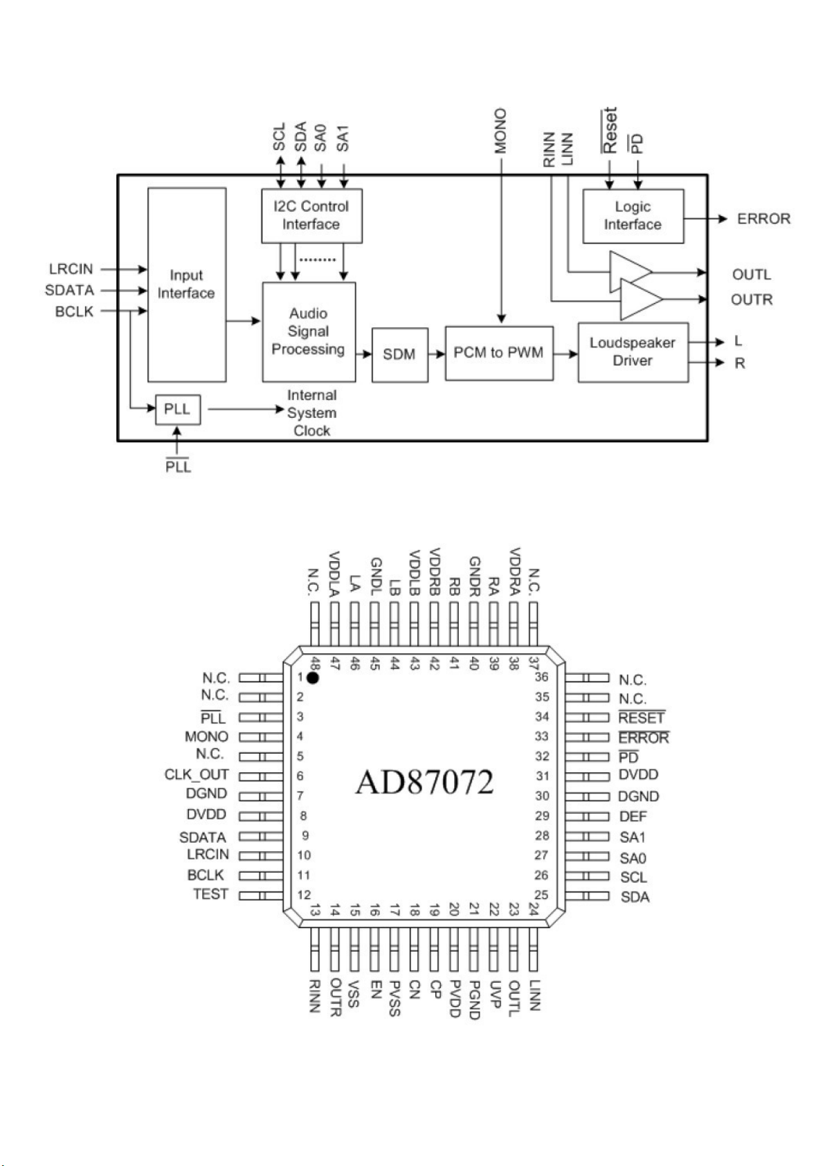
8.3 AD87072-LG48NRY (IC U601--AUDIO)

8.4 AD83586B-LG48NAY (IC U601--AUDIO)

8.5 ST53WS-13-E--LATAM (TU101)

9. Circuit Diagrams
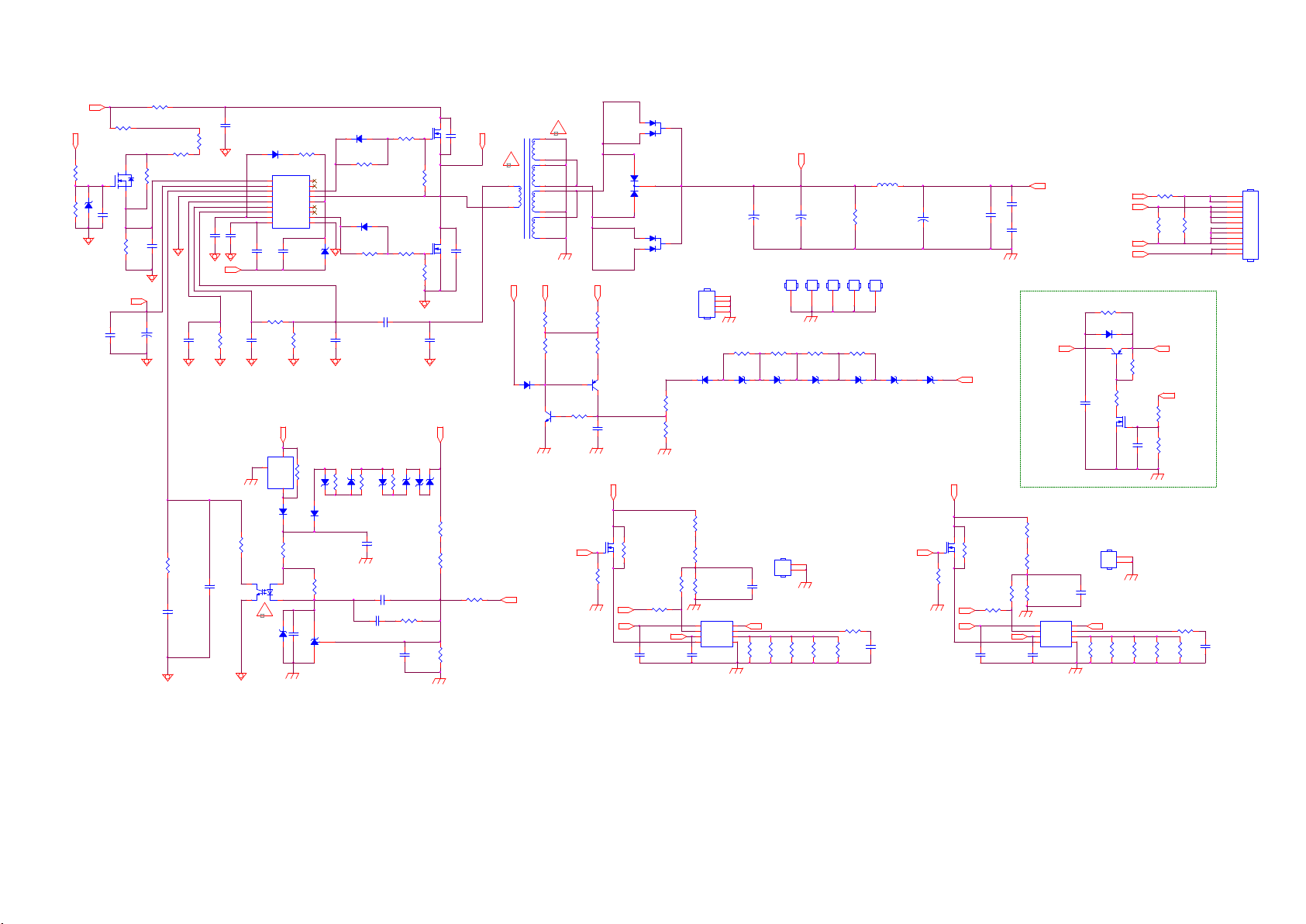
9.1 A 715G7374 PSU (For 55” 6233 Series)
9-1-1 AC Input
F9902
NC
!
T5AL/250V
F9901
1 2
3 4
FUSE
!
T5AH/250V
!
CN9902
NC
1
2
CN9901
AC 2P
!
U9901
NC
12
!
1D12D13NC4
NC
8
12
CN9904
NC
!
C9908
NC
NC5D26D27NC
CN9903
NC
L
C9913
220PF 250V
!
NR9901
t
NTCR 3.6W
RV9901
680V
12
!
!
FB9902
BEAD
N
R9907
R9906
510K
510K
510K
510K
R9905
R9904
510K
R9902
R9903
510K
!
12
FB9901
BEAD
C9911
22PF 250V
!
C9912
22PF 250V
12
C9901
470NF 275V
!
!
2
3
12mH
SG9902
500V
!
C9902
470NF 275V
1
L9901
4
!
!
NR9903
1 2
NTCR 3.6W
!
t
!
SG9901
500V
!
4
1
12mH
C9914
220PF 250V
3
2
L9902
!
1
2
3
4
L9903
0.25mH
L1N
2
NR9902
t
NTCR 3.6W
!
HS9901
HEAT SINK
For BD9901
12
4
1
2
!
-
BR
BD9901
2
TS25P06G-06
+
3
N
1
Vsin
L

9-1-2 PFC-LD7591T
D9801
D9803
C9801
47PF 1KV
VCC_ON
C9808
10UF 50V
Vsin
C9819
1uF 450V
R9819
0R05 1/4W
+
C9809
0.1uF 50V
FB9801
1 2
BEAD
0.1uF 50V
24KOHM +-1% 1/ 8W
C9806
1uF 450V
C9815
63
R9815
30K 1/8W 1%
R9801
0R05
C9807
47PF 50V
C9816
0.1uF 50V
R9813
S8KC
L9801
170uH
1 4
8
INV1COMP2RAMP3CS
5
6
OUT7VCC
GND
4
10K 1/8W
R9814
C9812
47nF 50V
R9807
2K 1% 1/8W
ZCD
R9802
10 OHM 1/ 4W
D9805
IN4148W RHG
LD7591T
U9801
D9806
IN4148W RHG
S8KC
1 2
FB9804
D9804
IN4148W RHG
R9803
33ohm 1/4W +/-5%
R9805
10K 1/8W
C9811
1NF
R9812
470R 1%
C9813
0.47UF 50V
BEAD
C9817
47PF 1KV
R9809
0.15R
FB9805
1 2
BEAD
1M 1% 1/4W
1M 1% 1/4W
R9818
0R05 1/4W
C9810
470PF 50V
R9806
R9804
R9810
1M 1% 1/4W
3
Q9802
NC
2
C9814
R9811
19K1 +-1% 1/8W
1
NC
C9803
+
68uF 450V
For Power Sav ing
R9817
R9816
NC
ZD9801
NC
1 2
For Q9 801 /D980 2
HS9801
HEAT SIN K
+
NC
C9804
68uF 450V
VCC_ON
1
2
3
4
HV
HV_A
R9821
NC
R9822
NC
C9820
NC
R9823
NC
R9824
NC
U9802
1
ISEN
2
GND
VSEN3IREF
NC
VCC
OUT
+VCC1
6
5
4
C9821
NC
R9825
NC
PFC_OVP
D9810
NC
D9802
FMNS-1106S
C9802
10NF 1KV
2
1
3
Q9801
IPA60R230P6
R9808
0.15R
C9818
470PF 250V
!
12
FB9802
BEAD

9-1-3 Standby-SSC3S121
HV
FB9101
1 2
BEAD
ZD9104
BZT52-B39
ZD9105
BZT52-B39
1 2
1 2
R9115
C9111
4.7nF 50V
BR
51K +-5% 1/8W
R9103
620K +-1% 1/4W
R9104
620K +-1% 1/4W
R9114
620K +-1% 1/4W
4.7M OHM +-5% 1/4W
R9116
0R05
U9101
1
FB/OLP
2
BR
ST4DRV
SSC3S121A
C9110
4.7uF 10V
C9101
1000PF
R9101
GND
VCC
OCP
C9108
470PF 50V
+VCC1
8
7
6
5
D9104
IN4148W R HG
R9111
200 OHM 1/4W
R9108
82 OHM
For Q9101
C9103
NC
SARS01-V1
R9109
10R 1/8W 5%
R9110
10K 1/8W
HS9101
HEAT SINK
R9106
33 OHM
D9101
1
2
3
4
Q9101
TK13A65U
C9102
2.2NF
R9119
33 OHM
D9103
SARS01-V1
R9112
0.24R
R9105
82K 2W
C9107
47PF 1KV
R9113
0R05
C9106
0.1uF 50V
D9102
FR107G-A0
+
HV_A
R9107
2 OHM 1%
+VCC1
C9104
100UF 50V
HOT
NC
!
U9102
EL817M(X)
C9131
1nF 250V
筿溃
DV5
12VS
+
(14V).
R9138
100K 1%
R9139
100K 1/8W 1%
C9144
NC
HS9103
HEAT SINK
+12V_A/+16V_A
+12V/+16V
L9102
3UH
C9146
2200uF 25V
C9147
C9148
+
C9142
1uF
NC
BL_ON/OFF
NC
C9141
1uF
+
NC
L9103
3UH
CN9103
CONN
16
15
14
13
12
11
10
9
8
7
6
5
4
3
2
1
+
1
2
3
4
C9126
+
220uF 25V
C9127
+
220uF 25V
R9137
0 OHM +-5% 1/8W
C9143
1N 50V
PS_ON
+12V_A/+16V_A
+12V/+16V
+12V/+16V
+12V_A/+16V_A
DIM
COLD
!
!
T9102
T9101
X'FMR 300uH
5
5
6
6
4
4
10
12
3
7
3
7
2
2
8
9
11
9
10
1
1
C9115
1NF 250V
!
12
FB9102
BEAD
R9130
27 OHM 1/4W
R9131
27 OHM 1/4W
R9132
27 OHM 1/4W
R9144
NC
12VS
R9146
2.2K 1/4W
R9147
12
43
1 2
ZD9102
BZT52-B20
C9140
1uF
2K2 1/8W 5%
U9104
TL431G-AE2-R
R9145
1K 1/8W 1%
C9139
0.47UF 50V
470R 1/8W 1%
D9106
FME-220B
D9107
FME-220B
D9108
FME-220B
R9133
27 OHM 1/4W
27 OHM 1/4W
27 OHM 1/4W
R9142
1.5KOHM
R9143
R9134
R9135
R9136
3
2
1
3
2
1
3
2
1
C9130
1nF 250V
NC
12VS
R9141
Standb y
9.1K 1%
R9140
9.1K 1%
Q9109
2N7002K
C9138
0.1uF 50V
R9117
+VCC1
3K
!
PFC_OVP
43
U9106
VCC_ON
Q9106
BTC4672M3
C9113
10UF 50V
R9118
20K 1/8W 1%
+
EL817M(X)
ZD9101
BZT52-B16
1 2
R9165
2K 1/8W 1%
R9166
0R05
12
DV5
LED_OVP
D9114
IN4148W R HG
R9164
3K
Q9108
MMBT3906
0.1uF 50V
R9163
10K 1/8W 1%
Q9107
2N7002K
C9129
R9162
1.5K OHM
C9145
100 OHM 1/4W
R9161
510K 1% 1/8W
R9160
12VS
NC
PS_ON
9-1-4 LED-SSC9522S+TPV101A or C
R8602 1M5 1/4W 1%
Q8603
3
NC
1
C8602 NC
2
R8605
18K 1/8W 1%
VCC_ON
C8605
10UF 50V
R8601 0.1R 1W
1M5 1/4W 1%
R8604
1M5 1/4W 1%
R8606
0R05 1/4W
C8603
0.1uF 50V
+
R8610
47K 1/8W 1%
R8603
C8607
4.7uF 10V
C8609
1UF
VBoot
C8608
0.47UF 50V
C8606
10N 50V
R8620
NC
C8601
1000PF
C8610
NC
D8603
1
2
3
4
5
6
7
8
C8611
5PF
R8619
470OHM +-5% 1/8W
C8613
1N 50V
U8605
NC
2
D8611
NC
R8609
470 OHM 1/4W
U8621
EL817M(X)
4
!
ZD8609
BZT52-B33
UF4007
U8601
Vsen
Vcc
FB
GND
Css
OC
RC
Reg
RV9COM
SSC9522S
+12V/+16V
3
GND
1
1
23
1 2
VCC_ON
R8607
NC
R8608 NC
NC
20150917 add.
0.1uF 50V
HV
ZD8615
1 2
C8604
10R 1/8W 5%
VGH
C8612
1uF
IN
OUT
R8638
1.5K OHM
R8611
NC
NC
VS
VB
NC
NC
VGL
ZD8601
BZT52-B15
R8618
270R 1%
R8674
NC
C8640
NC
18
17
16
15
14
13
12
11
10
1 2
0R05 1/4W
ZD8602
NC
12
D8609
IN4148W R HG
R8639
1K 1/8W 1%
U8604
TL431G-AE2-R
R8688
D8601
IN4148W R HG
R8612
47 +-5% 1/8W
D8602
IN4148W R HG
47 +-5% 1/8W
C8614
560PF 50V
R8687
0R05 1/4W
1 2
ZD8603
NC
R8615
ZD8604
NC
C8631
NC
100PF 50V
C8628
0.1uF 50V
C8616
100PF 1KV
R8686
0R05 1/4W
12
ZD8605
BZT52-B3V6
C8627
R8613
10R 1/8W 5 %
R8616
10 OHM 1/4W
10K 1/8W 1%
1 2
R8645
39K 1/8W 1%
Q8601
TK10A50D
TK10A50D
R8617
ZD8606
BZT52-B7V5
12
ZD8607
BZT52-B7V5
C8629
NC
R8614
10K 1/8W 1%
Q8602
VLED
1 2
C8617
33nF
R8640
47K 1/8W 1 %
R8641
47K 1/8W 1 %
R8642
7K5 1/8W +/-1%
VBoot
C8618
NC
X'FMR 310uH 50:10 f or 40V Back light
C8615
100PF 1KV
R8653
11K 1/8W 1%
!
1
4
LED_OVP
D8612
IN4148W R HG
MMBT3904
COMP
T8601
Q8608
!
5
12
6
11
9
7
10
8
DV5
R8643
0 OHM +-5% 1/8W
R8644
2K 1/8W 1%
1Kohm +-1% 1/4W
LED_VCC
Q8609
MMBT3906
R8648
R8625
+12V/+16V
NC
Q8607
NC
R8646
NC
R8647
1K 1/8W 1%
C8632
0.1uF 50V
-VLED-1
BL_ON/OFF
D8614
MBRF10150CT
3
2
1
1
D8615
NC
2
3
D8616
MBRF10150CT
3
2
1
R8631
5.1KR 1%
R8632
1K 1/8W 1%
R8622
JUMP
R8670
NC
R8671
0R05 1/4W
DIM
LED_VCC
C8625
NC C8626
0.1uF 50V
For D861 4/D8615 /D8616
HS8603
HEAT SINK
1
2
3
4
R8624
0R05
ZD8608
D8613
1 2
IN4148W R HG
NC
R8621
NC
R8623
NC
R8626
NC
U8602
TPV101AD
1
8
DIM
COMP
2
7
EN
GM
3
6
VCC
ISET
5
LED4GND
VLED
C8637
4.7UF
R8665
1oHM 1% 1/4W
CN8601
1
2
3
4
5
6
7
8
9
10
11
12
CONN
-VLED-1
-VLED-2
Q8605
+VLED
+VLED
R8650
NC
NC
C8636
1
2
R8662
1oHM 1% 1/4W
JUMPER
R8649
NC
NC
R8663
R8659
R8654
JUMP
R8667
NC
+12V/+16V
BL_ON/OFF
R8651
NC
R8660
0 OHM +-5% 1/8W
R8664
1oHM 1% 1/4W
R8666
NC
C8639
0.1uF 50V
C8633
0.1uF 50V
C8634
0.1uF 50V
+VLED
Opti on LE D_VC C控制 迴路 ,搭配 TPV1 11D使 用! !
R8669
0R05 1/4W
D8610
NC
LED_VCC
R8652
NC
R8656
NC
R8658
NC
1
2
3
U8603
TPV101AD
DIM
COMP
EN
VCC
LED4GND
ISET
Q8604
NC
NC
C8635
HS8602
HEAT SINK
C8648
NC
8
COMP
7
GM
6
1.2R 1%
5
1.2R 1%
R8661
L8601
C8620
+
NC
1 2
C8647
NC
COMP
1.2R 1%
R8633
1.2R 1%
R8627
0R05
ZD8610
NC
HS8601
HEAT SINK
GND1
NC
R8634
R8635
1oHM 1% 1/4W
1
1 2
1
2
+
GND2
NC
R8629
0R05
ZD8611
NC
C8621
220uF 100V
1
R8636
1oHM 1% 1/4W
GND3
GND
1
R8668
100K
GND4
GND5
GND
GND
1
R8630
0R05
ZD8612
1 2
NC
R8628
0 OHM +-5% 1/8W
R8637
1oHM 1% 1/4W
3UH
1
1 2
C8624
4.7UF
ZD8613
BZT52-B30
LED_VCC
+
ZD8614
1 2
BZT52-B30
R8657
NC
C8623
47uF 100V
Q8606
NC
-VLED-2
C8630
NC
R8655
JUMP
BL_ON/OFF
DIM
C8638
NC
VLED
R8672
NC
R8673
0 OHM 1/8W
LED_VCC

9.2 A 715G8886 PSU (For 55/65” OLED873 Series)
9-2-1 Input stage
FB9905
T5AH 250V
F9901
! !
CN9901
!
CONN
!
F9902
T5AH 250V
HEAT SINK
(for BD9902)
HS9901
(for BD9901)
HEAT SINK
BD_OUT-
C9920
NC/ 680PF 250V
BEAD
1 2
!
1 2
1
2
1 2
HS9902
1
2
3
4
680V
3 4
!
RV9901
3 4
TH3
1
2
3
4
NC/ FB9904
BEAD
!
BD_OUT-
C9901
NC/ 220PF 250V
C9902
NC/ 220PF 250V
NC/ FB9909
NC/ FB9910
12
!
TH9902
4
1
TH3
NTC R 2R 20% 3.6W
TH9905
1 2
1 2
BEAD
NTCR 2R 20% 3.6W
!
L9904
3
10uH
2
TH9906
NTCR 2R 20% 3.6W
BEAD
+VCC2
1K OHM 5% 1/8W
NTCR 2R 20% 3.6W
TH9901
470NF 305V
TH4
FB9906
TH9904
NTCR 2R 20% 3.6W
NTCR 2R 20% 3.6W
TH4
R9924
1M 1% R9925 1M 1%
R9927
R9914
C9903
BEAD
12
TH9903
SG9901
1
4
SG9902
BO
R9913 1M 1%
Q9902
MTN127KN3
10K 1/8W 1%
SW9901NC/ RELAY
3 1
4
DSPL-501N-A21F
!
!
2
C9904
3
8mH
L9901
470NF 305V
DSPL-501N-A21F
R99121M 1%
R9926
68K 1%
100P 50V
C9914
!
2
750K 1/4W
R9901
1D12D13NC4
U9901
CAP004DG-TL
8
!
R9903
750K 1/4W
!
IN4007-52 1 1000
D9901
IN4007-52 1 1000
1 2
C9915
2.2UF 50V
D9904
NC/ US1M_HF
750K 1/4W
R9902
!!
NC
R9904
750K 1/4W
+VCC2
D9902
D9903
SS1060FL
C9916
100N 50V
NC5D26D27NC
!
NC/ R9928
2 OHM 1% NC/ R9929 0R05
R9905 NC_3.9MOHM +-5% 1/2W
!
!
C9905
330PF 250V
C9910
100PF 500V
C9909
100PF 500V
!
L
N
1K OHM 1% 1/8W
2.2K OH M 1% 1/8W
1
4
C9906
330PF 250V
R9918
R9917
R9916
10K OHM 1% 1/8W
U9904
AS431AN-E1
!
8mH
L9902
L
L9903
4
2
1
3
10uH
N
EL817M(X)
1
2 3
CPH3351
Q9903
R9915
2K 1% 1/ 8W
!
!
U9903
3
2
DV5
4
-
!
!
4
-
4
R9923
12.7K OHM 1% 1/8W
2
+
3
3
+
2
0 OHM 1/8W
R9920
10K 1/8W 1%
BD9901
D25JAB60V
1
BD9902
D25JAB60V
1
BD_OUT-
R9921
12
FB9901
127R
BD_OUT+
12
FB9902
127R
+12V
ACD
C9918
4.7nF 50V

9-2-2 PFC stage
(For Q9804, D9806)
BD_OUT+
BD_OUT-
HS9801
1
2
3
4
HEAT SIN K
(for Q9803, D9805)
+VCC2
R9840
1K 1/4W
HS9802
1
2
3
4
1UF 4 50V
R9801
0.02R
BZT52-B18
NC/Z D9804
C9801
1 2
C9802
1UF 4 50V
R9802
0.02R
STD1NK60T4
R9841
10KOHM
Q9807
C9826
100N 50V
R9812
162K OHM 1% 1/8W
M+
!
811
L9801
450uH
ZCD A
!
811
L9802
450uH
ZCD B
R9809
3.3M OHM 1% 1/ 4W
R9810
3.3M OHM 1% 1/ 4W
R9811
3.3M OHM 1% 1/ 4W
ZCD B
VSENSE
HVSEN
C9811
1NF 50V
2
10
GDA
2
10
GDB
+VCC2
R9813
24K 1/8W 1%
R9814
124K 1%
C9812
68P 50V
R9806
22R 1%
C9815
68N 50V
R9803
22R 1%
1 2
C9813
22uF 50V
1
2
3
4
5
6
7
D9804
SS1060FL
U9801
UCC 28063DR
D9801
S8KC
D9803
SS1060FL
1 2
R9804
22R 1%
Q9801
MMBT2907A
R9807
22R 1%
Q9802
MMBT2907A
+
C9814
100NF 50V
ZCD B
VSENSE
TSET
PHB
COMP
AGND
VINAC
HVSEN8PWMCNTL
10K 1/8W 1%
R9815
47K 1/8W 1%
ZCD A
VREF
PGND
R9816
C9816
0.47uf 10% 50V
GDA
VCC
GDB
D9802
S8KC
R9805
10K 1/4W
R9808
10K 1/4W
CS
ZD9803
BZT52-B3V6
FB9801
1 2
127R
Q9803
TK39A60W
FB9802
Q9804
TK39A60W
16
15
14
13
12
11
10
9
GDA
GDB
12
C9817
3.3NF 50V
C9803
100PF
12
127R
C9805
100PF
C9819
220NF 5 0V
R9818
330R 1/ 8W 5%
C9804
100PF
D9805
FMN-1106S
C9806
100PF
D9806
FMN-1106S
C9818
68P 50V
R9817
24K 1/8W 1%
HVSEN
ZCD A
BD_OUT-
C9807
470PF
R9820
2M 1%
R9821
2M 1%
R9822
2M 1%
R9823
NC R9831
C9820
1NF 50V
Q9805
STD1NK60T4
C9821
100N 50V
R9824
82K 1% 1/ 8W
C9808
10NF 1KV
R9819
2M 1%
!
+
C9810
150uF 450V
R9825
2M 1%
R9826
2M 1%
1K 1/4W
R9832
10KOHM
+VCC2
B+
!
C9809
+
150uF 450V
R9827
2M 1%
R9828
2M 1%
R9829
NC
VSENSE
C9822
1 2
1NF 50V
BZT52-B18
NC/Z D9801
Q9806
STD1NK60T4
R9830
124K 1%
C9823
100N 50V
R9833
1K 1/4W
R9834
10KOHM
1 2
BZT52-B18
NC/Z D9802
HEAT SIN K

9-2-3 12V power stage
B+
+VCC1
+VCC2
+VCC2
+VCC3
C9119
10UF 50V
C9120
10UF 50V
150K 1% 1/8W
C9101
2.2NF
+
+
R9104
C9102
330nF
10nf 10% 50v
R9113
51K 1/8W 1%
C9105
100NF 50V
C9107
220pF 5% 50V
R9114
82 OHM
Q9104
BTC4672M3
Q9105
BTC4672M3
C9104
R9116
100K 1/8W 1%
R9120
3K
R9121
R9122
3K
R9123
R9103
1M 1%
R9105
20M
NC/20K
NC/20K
3.3M 1/4W
FB_LL C
C9106
0.47uF 50V
CL
R9115
120 OHM 5% 1/8W
STB
HOT
!
U9105
EL817M(X)
4
ZD9102
BZT52-B18
1 2
!
U9106
EL817M(X)
4
ZD9103
BZT52-B16
1 2
R9102
COLD
LLC_OVP
R9101
3.3M 1/4W
47K +-5% 1/8W
R9145
2K OHM 1% 1/8W
1
23
R9151
2K OHM 1% 1/8W
1
23
Q9103
MMBT3906
R9117
C9114
4N7 50V
D9101
1N4007
C9103
1NF
U9101
SSC3S910
1
VSEN
2
VCC
3
FB
4
ADJ
5
CSS
6
CL
7
RC
8
PL
SB9GND
C9113
10nf 10% 50v
DV5
R9148
R9154
C9118
10N 50V
10KOHM
10KOHM
Bo
ST
NC
VGH
VS
VB
NC
REG
VGL
Q9111
MMBT3906
Q9114
MMBT3906
18
17
16
15
14
13
12
11
10
R9118
47K +-5% 1/8W
4
R9147
10KOHM
Q9112
2N7002K
R9153
10KOHM
Q9113
2N7002K
R9119
10KOHM
C9144
C9145
U9103
EL817M(X)
R9146
1K5
100N 50V
R9152
1K5
100N 50V
R9106
10R 1/8W 5%
C9108
100NF 50V
D9103
10R 1/8W 5%
R9110
REG
C9115
2.2UF 10% 25 V
+12VS
1
23
!
R9150
510K
R9156
510K
D9102
1N4148W
R9107
82 OHM
10KOHM
12
ZD9101
BZT52-B15
R9109
2R2 +-5% 1/8W
D9104
US1M_HF
1N4148W C9110
R9111
82 OHM
10KOHM
+VCC1
C9116
100NF 50V
R9142
5.1K
R9144
Q9110
100R
2N7002K
R9143
C9143
510K
100N 50V
+12VS
R9149
100R
PS_ON/OFF
DV5
R9930
0 OHM 1/8W
ACD
R9155
100R
PANEL_ON/OFF
L9101
+12VS
3.0uH+-10%
R9178 10K 1/8 W 1%
ZD9107
BZT52-B4V7
1 2
C9129 47PF 50V
+12V
+12V
VD24VSS
3
EN
2
PGND
1
VG2
MP6922LGS-Z
3.0uH+-10%
VD1
VDD
VG1
U9102
R9163
9.1K OHM 1% 1/8W
R9165
2K 1/8W 1%
R9166
1.8K OHM 1% 1/8W
L9102
5
6
7
8
R9132
47K 1/8W 1%
R9164
5K6 +-1% 1/8W
C9126
470UF 25V
DV5
NC/R9179
10K 1/8W 1%
NC/C9150
R9131
2R2 +-5% 1/8W
R9138
30K 1/8W 1
C9133
NC/2.2UF 50V
C9134 1uF 50V
NC/Q9118
MMBT3906
100NF 50V
2N7002K
C9127
+
470UF 25V
R9134
1K OHM 1% 1/8W
R9133
10 OHM 1% 1/8W
TK58A06N1
C9130
2.2UF 50V
47PF 50V
MTB5D0P03FP-0-UB-S
Q9109
R9139
NC/R9180
33K 1/8W 1%
0.1uF 50V
Standby
Q9116
C9142
100N 50V
Q9107
NC/D9110 SS1060FL
C9146
R9167
100R
R9168
+
12
510K
C9149
470UF 25V
47K 1/8W 1%
1 2
NC/D9109
R9181
NC/47K 1/ 8W 1%
+
D9108
1 2
SS1060FL
SS1060FL
PS_ON/OFF
ACD
0.1uF 50V
100N 50V
+12V
R9135
NC/ 10 OHM 1% 1/4W
C9132
NC/1nF 50V
L9103
3.0uH+-10%
Q9117
2N7002K
C9138
100NF 50V
C9147
C9922
+12V
DV5
+
C9135
470UF 25V
1 2
R9140
510K 1% 1/8W
CN9101
2
4
6
8
10
12
14
16
15
13
11
9
7
5
3
1
CN9103 NC/C ONN
CN9102
CONN
C9136
470UF 25V
R9141
100R
D9106
SS1060FL
CONN
1
2
3
4
5
6
7
8
9
10
11
12
13
14
+
1
3
5
7
9
11
13
15
HS9102
HEAT SINK
HS9103
HEAT SINK
C9137
0.1uF 50V
T-CON_ON/OFF
16
14
12
10
8
6
4
2
1
2
3
4
1
2
3
4
+12V_T
+12V+12V
T-CON_ON/OFF
PANEL_ON/OFF
+12V_T
+24V_A+24V_A
HOT COLD
+
+
+
C9124
C9125
1500uF 25V
1500uF 25V
R9127
1K OHM 1% 1/8W
R91292R2 +-5% 1/8W
TK58A06N1
R9130
47K 1/8W 1% C9131
C9139
10N 50V
C9140
NC/47N 50V
C9141
R9162
100NF 50V
30K 1/8W 1
AS431AN-E1
U9108
7
8
12
9
10
11
C9908
1NF 250V
!
NC/680PF 250V
NC/680PF 250V
R9157
2K 1/8W 5%
1
23
Q9106
+12VS
1 2
12
R9159
1K 1/8W 1%
C9123
1500uF 25V
R9128
NC/10 OHM 1% 1/4W
C9128
NC/1nF 50V
ZD9106
BZT52-B15
D9107
SS1060
R9158
100 OHM 1%
C9109
1NF
Q9101
TK13A50D
R9108
Q9102
100PF
TK13A50D
R9112
C9148
47uF 100V
+
+
C9117
47uF 100V
HS9101
HEAT SINK
D9105
US1M_HF
1
2
3
4
C9111
C9112
15nF
100PF
R9172
2R2 1%
DV5
CL
10K 1/8W 1%
ZD9104
BZT52-B5V6
1 2
R9124
!
6
4
2
1
+VCC1
4
HOT
T9101
POWER X'FMR
FB9903
127R
C9919
C9921
U9104
EL817M(X)
COLD
12
!
!
!
Q9115
MMBT3904
+12VS
FB_LL C
R9125
R9126
1K 1/8W 1%
0R05 1/8W
!
R9160
U9107
EL817M(X)
1
4
1N 50V
C9122
C9121
220N 50V
ZD9105
BZT52-B15
23
1 2
4.7K
R9161
3.9K OHM 1% 1/8W

9-2-4 24V power stage
R9254
10K 1/8W 1%
C9202
100NF 50V
R9253
+VCC3
B+
R92041.5M OHM 1% 1/4W
1K 1/8W 1%
R9252
NC/0R 05
Q9209
C9242
0.1UF 50V
R9205
18K 1/8W 1%
STD1NK60T4
C9201
10NF 1KV
R9203 1.5M 1%
+VCC3
C9203
22uF 50V
C9205
0.47uf 10% 50V
R9201 0R1
R9202 1.5M 1%
+
100NF 50V
1nF 50V
C9204
C9206
47P 50V
C9243
U9201
1
Vsen
2
Vcc
3
FB
4
GND
5
Css
6
OC
7
RC
8
Reg
RV9COM
SSC9522S
R9267 0R 1
C9247
10NF 1KV
NC
NC
VGH
VS
VB
NC
NC
VGL
D9203
C9212
1nF 50V
C9209
1UF
18
17
16
15
14
13
12
11
10
B+
D9208NC/FR 107G-A0
D9201 SS1060FL
R9206
10 OHM 1/8W
R9207
68OHM +-5% 1/8W
D9202
SS1060FL
R9209
10 OHM 1/8W
R9210
68OHM +-5% 1/8W
US1M_HF
R9213
1K 1/8W 1%
180 OHM 1% 1/8W
M+
12
10K 1/8W
12
10K 1/8W
R9212
10R 1/8W 5%
C9210
10PF 3KV
R9208
R9211
R9214
C9208
1UF
C9213
100PF
Q9201
IPA50R190CE
C9207
330PF
Q9202
IPA50R190CE
ZD9201
BZT52-B15
1 2
C9211
10PF 3KV
C9214
900R 5%
R9264
900R 5%
R9272
R9273
R9265
2K4
2K4
T9201
!
POWER X'FMR
!
T9202
POWER X'FMR
7
11
12
8
9
10
7
11
12
8
9
10
5
6
1
2
5
6
1
2
C9215
27nF
27nF
R9231
R9266
900R 5%
10 OHM 1% 1/4W
C9226
1nF 250V
10 OHM 1% 1/4W
C9231
1nF 250V
C9219
C9220
+
1000UF 35V
R9220
1K OHM 1% 1/8 W
R9221
TK56A12N1
Q9203
R9223
R9229
1K OHM 1% 1/8 W
Q9205
TK56A12N1
R9233
47K 1/8W 1%
+24VS
+
1000UF 35V
R9222
2R2 +-5% 1/8W
R9232
2R2 +-5% 1/8W
1000UF 35V
47K 1/8W 1%
C9221
+
L9201
3.0uH+-10%
L9202
3.0uH+-10%
C9222
+
1000UF 35V
3
2
1
C9227
NC/10PF 50V
3
2
1
C9232
NC/10PF 50V
470UF 35V
U9202
VD24VSS
EN
VD1
PGND
VDD
VG2
VG1
MP6922LGS-Z
U9203
VD24VSS
EN
VD1
PGND
VDD
VG2
VG1
MP6922LGS-Z
C9223
+
5
6
7
8
5
6
7
8
47K 1/8W 1%
R9217
5.1KR 1%
C9224470UF 35V
+
+
R9224
2R2 +-5% 1/8W
R9225
47K 1/8W 1%
R9234
2R2 +-5% 1/8W
R9235
5.1KR 1%
C9246
470UF 35V
C9228
NC/10PF 50V
C9233
NC/10PF 50V
R9218
R9259
R9219
5.1KR 1%
R9226
1K OHM 1% 1/8 W
R9227
10 OHM 1% 1/8W
TK56A12N1
C9229
2.2UF 50V
R9236
1K OHM 1% 1/8W
R9237
10 OHM 1% 1/8W
TK56A12N1
C9234
2.2UF 50V
900R 5%
Q9204
Q9206
R9258
900R 5%
R9263
R9260
900R 5%
900R 5%
MP6922
R9228
10 OHM 1% 1/4W
C9230
1nF 250V
MP6922
R9238
10 OHM 1% 1/4W
C9235
1nF 250V
+24V
C9225
0.47UF 50 V
HS9201
HEAT SINK
R9268
R9269
2K4
2K4
CN9202
NC/C ONN
MP6922
1
2
3
4
1
2
3
4
5
6
7
8
9
10
11
12
13
14
15
R9270
R9271
2K4
2K4
U9206
OUT3IN
2
HS9202
HEAT SINK
CN9201
1
2
3
4
5
6
7
8
9
10
11
12
13
14
15
CONN
+24V
1
+24VS
GND
HS9203
HEAT SINK
1
2
3
4
1
2
3
4
+24V
R9215
2K4 +/-1% 1/8W
C9217
4.7UF 25V
560 OHM 1/8W
R9216
C9216
10nf 10% 50v
R9245
!
12
43
U9204
EL817M(X)
ZD9204
BZT52-B22
1 2
R9243
R9244
100 OHM 1%
10K 1/8W 1%
2.4K OHM 1% 1/8W
D9205
IN4148W R HG
D9204
IN4148W R HG
C9241
470NF 50V
1 2
ZD9203
BZT52-B5V6
C9240
100NF 50V
U9205
AS431AN-E1
R9261
C9239
NC
0R05
1 2
ZD9202
NC/BZ T52-B5V6G
R9242
1K 1/8W 1%
+24VS
+24V
R9239
15K 1/8W 1%
R9240
2K 1/8W 1%
1.96K OHM 1% 1/ 8W
R9241
R9262
NC/82K 1% 1/8W
+12VSDV5LLC_OVP
D9206
SS1060FL
+24V
R9255
R9256
R9257
R9173
R9174
R9175
R9176
R9177
R9248
0R05 1/8W
R9249
R9250
1K OHM 1% 1/8W
Q9207
MMBT3906
C9236
100NF 50V
ZD9205
BZT52-B15
1 2
ZD9206
BZT52-B15
1 2
12
R9251
1K 1/8W 1%
D9207
SS1060FL
+24VS +24V_A
+12VS
R9246
NC
12
R9247
2K 1/8W 1%
Q9208
MMBT3904
1K OHM 1% 1/8 W
0R05
0R05
0R05
0R05
0R05
0R05
0R05
0R05
L9204
3.0uH+-10%
L9203
3.0uH+-10%
C9238
+
C9237
0.47UF 5 0V
470UF 35V
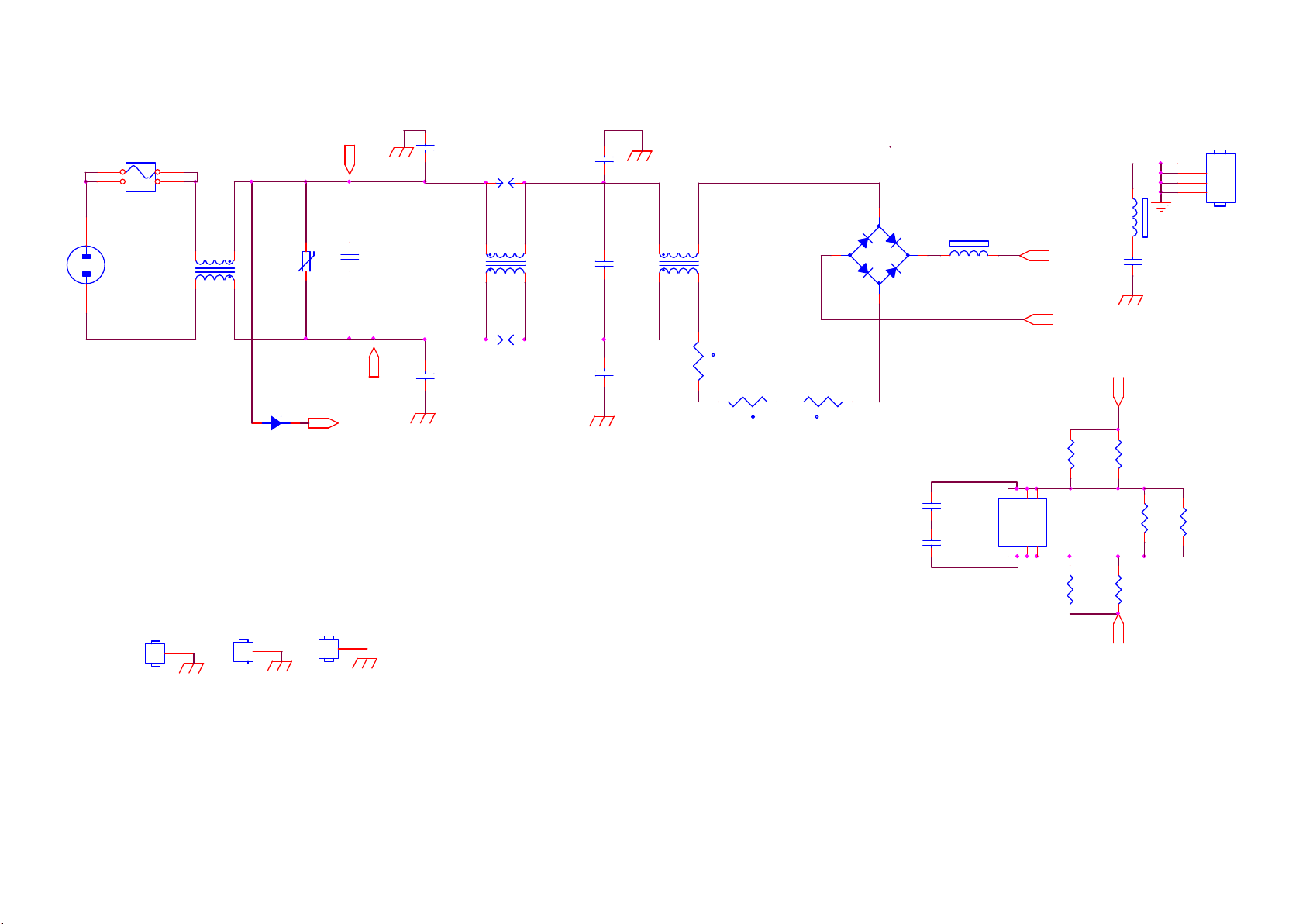
9.3 A 715G9309 PSU (For 50” 6233 Series)
9-3-1 AC Input
12
F9901
FUSE
1 2
3 4
T5AH / 250V
CN9901
AC 2P
0.25mH
L9904
1
2
3
680V
4
RV9901
1
470NF 275V
C9901
C9911
220PF 250V
DSPL-501N-A21F
SG9901
1
4
2
3
L9902
17mH
C9902
470NF 275V
C9913
220PF 250V
1
4
2
3
L9903
17mH
EU & CN BD9901: 393G0050460607 / 393G0050460604 (
AP BD9901: 393G0050460602 / 393G0050460600 (
3
4
-
2
BD9901
GBJ1008-FUN
1
1 2
+
FB9901
BEAD
ぃ床荐
床荐
Vsin
)
)
FB9904
127R
1 2
GND
C9915
470pF 250V
HS9901
NC/ HEAT SIN K
1
2
3
4
Rsen-
1.5R
t
1 2
1 2
1.5R
NR9901
2
NR9903
1.5R
12
C9904
100PF 500V
C9903
100PF 500V
1D12D13NC4
NC
8
U9901
CAP200DG-TL
NC5D26D27NC
R9903
R9904
750K +-5% 1/4W
750K +-5% 1/4W
R9905
R9906
NC/ 750K +-5% 1/4W
NC/ 750K +-5% 1/4W
t
t
D9901
PG4007
BR
SG9902
DSPL-501N-A21F
C9912
2
220PF 250V
C9914
220PF 250V
NR9902
GND1
1
GND
GND2
1
GND
GND3
750K +-5% 1/4W
R9901
1
GND
750K +-5% 1/4W
R9902
1

9-3-2 PFC with LD7592S
EU & CN L9801:373G0174427H0000VP / EQ32
AP L9802:373G0174428H0000VP / EQ40
C9805
NC/ 47PF
Vsin
4
1
C9804
1uF 450V
Rsen-
HVvcc
PFC_VCC
R9819
0 OHM 5% 1/8W
C9808
+
10uF 50V
C9815
100N 50V
GND
12K 1/8W 1%
EU & CN R9813:12K
AP R9813:22K
C9810
470PF 50V
GND
5
L9801
E1
240uH
6
4
3
NC/170uH
L9802
1
GND
R9803
33 OHM 1/ 4W
D9805
SS1060FL
D9804
SS1060FL
Q9803
MMBT2907A
R9802
47OHM +-5% 1/8W
1
10KOHM
R9805
D9801
FMNS-1106S
2
3
Q9801
IPA60R190P6
C9817
100PF
C9806
10NF 1KV
GND
C9801
+
47UF 450V
GND
C9802
+
47UF 450V
GND
C9803
+
47UF 450V
GND
R9804
1.5M 1%
R9806
1.5M 1%
GND
GND
R9808
0R05
R9809
NC/0R05
HS9801
HEAT SINK
For Q9801
HV
1
2
3
4
GND
R9899
R9818
2.7K 1%
Q9802
MTN127KN3
R9811
1K OHM 1%
R9817
10K 1/4W
NC
C9814
ZD9801
100P 50V
1 2
R9816
100K 1/8W
PFC_V CC
GND
R9813
GND
8
OUT7VCC
INV1RAMP2COMP3CS
5
6
GND
4
C9812
47N 50V
GND
U9801
LD7592
OVP
10K 1/8W
R9814
C9813
0.47UF 50V
GND
R9801
18K 1%
NC/0R05
GND

9-3-3 LLC with SSC3S927
HV
ADJ
PFC_VCC
100K 1%
R9166
BZT52-B16
C9101
1NF
ZD9152
GND
10N 50V
C9104
D9102
1N4148W
GND
Q9105
BTC4672M3
2Kohm 1/4W +/ -1%
1 2
GND
R9103
36K 1/8W 1%
51K 1/8W 1%
220NF 50V
220P 50V
200R 1/8W 1%
R9165
0R05 1/4W
R9168
C9102
2.2nF 50V
R9104
C9105
C9107
R9105
R9180
100K 1/8W 1%
C9180
220nF50V
STB
R9106
Q9106
MMBT3906
R9102
0R05 1/4W
FB_LLC
C9106
0.47UF 50V
CL
120R 1/8W 1%
VCC1
R9101
3M 1%
NC
R9107
100K 1/8W 1%
R9113
C9121
10N 50V
R9112
100K 1%
Q9107
LMBT3904LT1G
C9118
0.47UF 50V
R9111
100K 1%
Q9108
MMBT3906
LLC_OVP
R9167
200K 1% 1/8W
R9100
C9100
NC/1NF
GND
R9122
NC/10M
4N7 50V
R9169
100K 1/8W 1%
C9109
10N 50V
3M 1%
C9110
REG
1
2
3
4
5
6
7
8
U9101
SSC3S927
R9147
VSEN
VCC
FB
ADJ
CSS
CL
RC
CD
SB9GND
ZD9142
1 2
47K 1/8W 1%
ADJ
BZT52-B6V2
BR
R9192
1KR
18
ST
17
NC
16
100N 50V
VGH
15
VS
14
VB
13
NC
12
REG
11
VGL
10
ZD9141
BZT52-B15
1 2
HOT COLD
C9120
10N 50V
R9148
10K OHM
REG
R9191
1KR
R9118
10 OHM 1% 1/8W
C9114
D9101
US1M_HF
R9115
10 OHM 1% 1/4W
REG
C9115
2.2uF 25V
R9120
2R2 +-5% 1/8W
75 OHM 1% 1/8W
GND
D9104
SS1060FL
R9117
75 OHM 1% 1/8W
12
ZD9101
BZT52-B15G
D9103
SS1060FL
R9114
HS9101
1
2
3
4
HOT
HEAT SINK
T9101: 380GL52 P370H00 00VP / 12V & 2 4V
GND
T9101: 380GL52 P369H00 00VP / 12V & 3 6V
T9101: 380GL52 P368H00 00VP / 12V & 4 2V
Q9101
C9199
IPA50R190CE
100PF
C9111
100PF
Q9102
IPA50R190CE
+
C9116
100UF 50V
C9112
27nF
D9105
FR107G-A0
C9113
100PF
R9108
0.05R 1%
R9119
10K OHM
R9116
10K OHM
2
1
3
2
1
3
GND
12
12
VCC1
FB_LLC
R9164
4K7 1/8W 1%
47N 50V
C9156
GND
COLD
D9124
1
FMEN-2308
3
1
3
1
3
D9122
FCQS20A065
2
D9121
FCQS20A065
2
3
1
2
D9125
FMEN-2308
2
GND
T9101
!
2
3
13
14
POWER X'FMR
C9161
330PF 250V
12
8
11
6
10
7
9
5
12VS
0R05
R9163
R9162
1.5K OHM
R9161
4K7 1/8W 1%
12
43
1N 50V
C9155
U9104
EL817M(X)
!
1 2
ZD9153
BZT52-B13G
C9157
1UF 50V
C9153
100N 50V
U9150
AS431AN-E1
C9152
47N 50V
R9160
12K 1/8W 1%
DV5
R9146
2Kohm 1/4W +/- 1%
12
43
U9103
EL817M(X)
!
GND
R9145
10K OHM
Q9142
MMBT3906
R9143
10K OHM
Q9141
2N7002K
C9141
R9144
1K5 1% 1/8W
100N 50V
C9148
100NF 50V
R9142
+
C9126
470uF 20% 25V
12VS
510K 1% 1/8W
12V/7A
R9156
R9157
10K 1/8W 1%
R9158
2K49 1/8W 1%
R9159
200 OHM 1% 1/8W
12VS
R9141
100 OHM 1%
+
C9133
100u 100V
12VS
C9127
+
470uF 20% 25V
0R05 1/8W
36V
+
R9153
5K1 1/8W 1%
PS_ON
C9134
100u 100V
+
C9128
470uF 20% 25V
+
Q9151
2N7002K
C9138
100u 100V
L9121
1.1uH
Boost_ Vin
R9194
5K1 1/8W 1%
R9195
43K2 +-1% 1/8W
R9151
100 OHM 1%
C9151
R9152
100N 50V
510K 1% 1/8W
R9172
R9174
R9173
10K 1/4W
Q9131
MTE1K8N25KM3-0-T2-G
R9175
10K 1/4W
10K 1/4W
10K 1/4W
C9136
R9170
100N 50V
510K 1% 1/8W
+
C9130
47uF 50V
Boost 24 V R919 4:5.1K
Boost 30 V R919 4:33K
Boost 42 V R919 4:43.2 K
DV5
R9171
100R 1%
R9176
10K 1/4W
C9131
100N 50V
R9177
10K 1/4W
C9132
100N 50V
R9178
10K 1/4W
DV5
C9124
100N 50V
BL_ON/OFF
+12V_A
+12V
+12V
R9179
10K 1/4W
C9135
100N 50V
+12V_ A
C9125
100N 50V
HS9124
HEAT SINK
For D9124 & D9125
HS9121
HEAT SINK
For D9121 & D9122
CN9102
CONN
15
13
11
9
7
5
3
1
Boost_Vin
C9137
100N 50V
1
2
3
4
1
2
3
4
Α
16
14
12
10
8
6
4
2
DIM
PS_ON
+12V_A
+12V+12V
+12V

9-3-4 Driver with PF7909S
Boost_Vin
L8601
33uH
3
C8611
1UF 50V
1
BL_ON/OFF
C8607
100N 50V
DIM
R8623
5K1 1/8W 1%
R8614
1K8 1% 1/8W
R8608
1K OHM 5% 1/8W
10N 50V
C8608
R8609
0 OHM +-5% 1/8W
0 OHM +-5% 1/8W
R8610
R8613
150K 1% 1/8W
+12V
VREF
C8610
1UF 50V
10 OHM 1/4W
LED_FB
14
13
12
11
10
C8609
1N 50V-NC
R8612
200KOHM 1/8W +/-5%
VREF
CN8601
CONN
12
11
D8601
3
FMEN-2308
2
R8617
510K 1% 1/8W
R8618
510K OHM 1% 1/4W
2.5V
R8619
62K 1/8W 1%
R8620
100R 1/8W 5%
R8622
100 OHM 1/4W
C8604
2.2NF 200V
R8619 / 62K / OVP 43V
R8619 / 33K / OVP 79V
-VLED
1
R8621
10K OHM +-5% 1/8W
1
R8607
C8612
C8615
1UF 50V
100N 50V
DIMOUT
U8601
PF7909S
1
DIMOUT
FB
2
VCC
GM
3
CS
ADIM
4
OUT
VREF
5
GND
FLAG
9
8
6
OVP
EN
7
RT
DIM
FLAG
R8611
180K 1% 1/8W
C8614
1NF 50V
LED_OVP
R8604
10R 1/8W 5%
R8603
33R 1/8W 5%
D8602
SS1060FL
10K OHM +-5% 1/8W
R8606
1.5K 1/4W
C8613
1NF 500V
HS8601
1
2
3
4
HEAT SINK
R8605
12
Q8601
MTE011N10RFP-0-UB-S
C8606
NC/47PF
R8601
0.03R
R8615
LED_OVP
DIMOUT
R8616
NC/47K 1/4W
NC/47K 1/4W
LED_FB
+
C8601
100u 100V
Q8602
MTD030N10QJ3 100V
3 2
0.3125V
R8631
0.25R 1%
R8632
0.25R 1%
+
C8602
100u 100V
R8633
0.25R 1%
+
R8634
0.25R 1%
FB8601
BEAD
1 2
C8603
100u 100V
+VLED
-VLED
+VLED
10
9
8
7
6
5
4
3
2
1
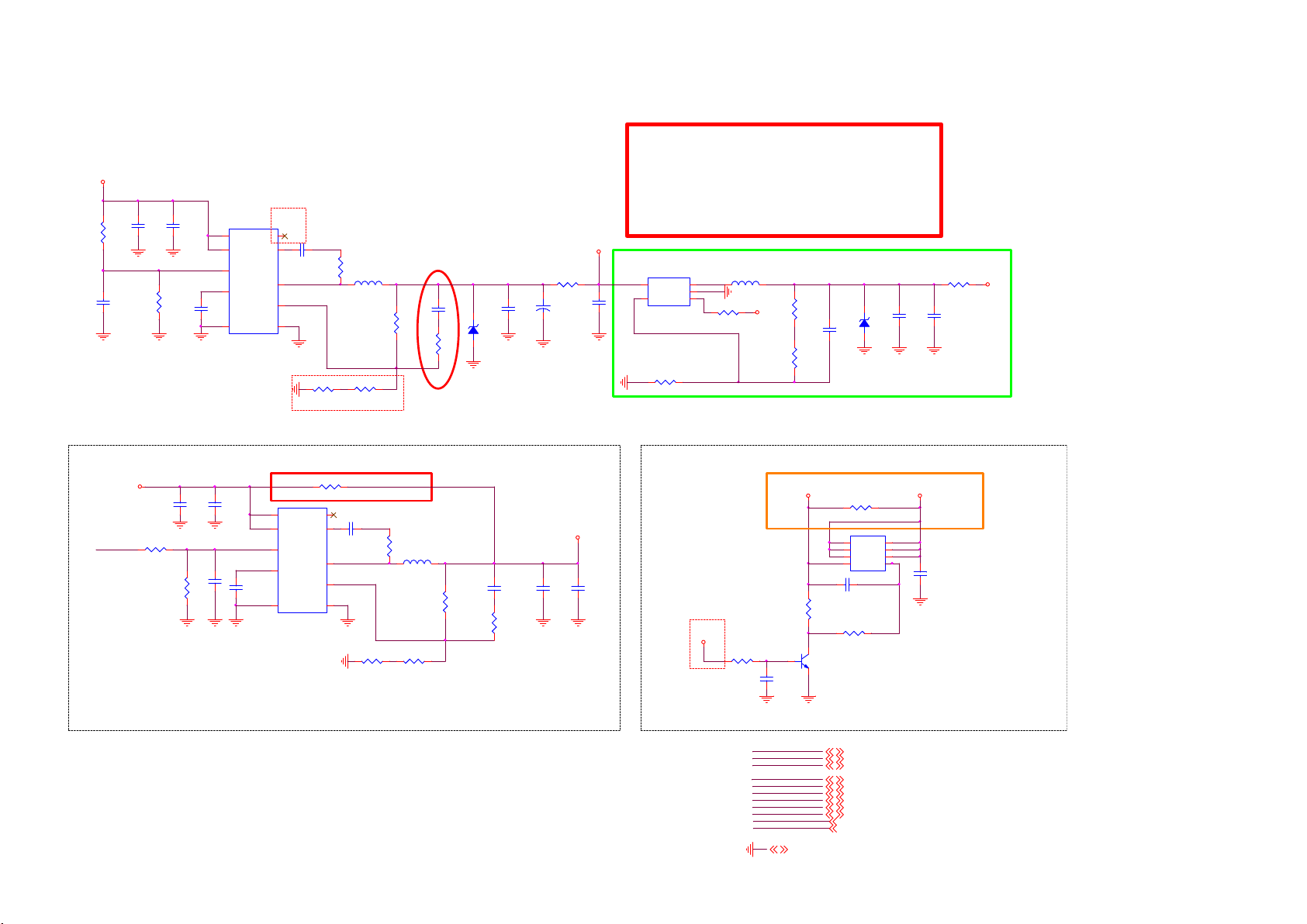
9.4 B 715G8709 SSB (For 50/55” 6233 series)
9-4-1 POWER
2K17 MT5802 platform
Main_18V_12V
Big p lane
R798
100K 1/16W 5%
C778
C779
10UF 16V
10UF 16V
C777
NC/100N F 25V C780
Vout = 0.6V (1+( R1/R2
))
Vout = 0.6V (1+( 100/(10+3.3)
))=5.19V
R744
33K 1/16W ZD706
⊙
⊙
8
7
1
5
4.7UF 6.3V
9
U708
IN
IN
EN
VC
GND
SY8366QNC
6A(Spec.)
ILMT
2
PG
C781
6
BS
100N 50V
10
LX
4
FB
3
Big p la ne
R796
10K 1%
R2
R745
2.2R 1%
3K3 1%
L702
3.3UH
R1
R795
R794
+5V_STB
U707
SY8089AAAC
4
IN
5
FB
R742
LX
GND
EN
2A
R2
18K OHM 1%
3
2
1
R748
4.7K1/16W
L704
C787
22UF 10V
+
R782
C702
100UF 16V
0R05
C724
2.2UF 10V
Big p lane
C785
100K 1/10W 1%
3N9 50V
R703
1K 1/10W 1%
MAX=3A
ZD704
NC/R LZ6V2B
1 2
2.95A
2.2uH
+5V_STB
R1
R746
75K 1/16W 1%
C711
33P 50V
R751
6K2 1/10W 1%
R750
3V3SB
0R05 1/8W
C729
C725
NC/B ZT52-B3V6
1 2
10UF 10V
NC/10U F 10V
Main_18V_12V
OPWRSB_PWR
MAX=2.3A
R786
NC/10K 1/16W 5%
C766
NC/10U F 25V
R787
Big p la ne
C767
C768
NC/10 0K 1/16W 5%
NC/10U F 25V
NC/10 0N16V
C769
NC/4. 7UF 6.3V
U701
8
IN
7
IN
1
EN
5
VC
9
GND
NC/S Y8366QNC
6A(Spec.)
Vout = 0.6V (1+( R1/R2
))
Vout = 0.6V (1+( 100/(5.1+0.16)
))=12V
⊙
⊙
R783 0R05
2
PG
C770
6
BS
NC/100N 50V
10
LX
4
FB
3
ILMT
R7047
NC/2. 2R 1%
Big p la ne
R2
R791
NC/160R 1/16W
L705
NC/3.3UH
R1
R790
NC/5. 1K 1%
Big p la ne
18V_12V
MAX=3A
R789
NC/100K 1/10W 1%
R792
NC/1K 1/10W 1%
C771
NC/470PF
NC/10 UF 25V
C774
16V to 12V for Panel Vcc
For PSU 16V only
C775
R781
+5V_SW+5V_STB
NC/0R 05
MAX=2.0A
Q706
8
7
6
+5V_STB TO +5 V_SW BY VCCK
NC/10 UF 25V
VCCK
R740
1K 1/16W 5%
C701
100N 16V
18V_12V
+5V_STB
VCCK
DDRV
DVDD 3V3
3V3SB
+5V_SW
AVDD1V0_1
AVDD1V0_STB
OPWRSB
OPWRSB_PWR
GND 5, 6,7,8,9,10, 11,12,13,14,15,16,17, 18,19,20,21,22
5
C716
1UF 16V
R733
33K 1/10W 5%
R738
22KOHM 1/10W
Q707
BC847N3
OPWRSB 5,6
OPWRSB_PWR 5,18,22
1
D
D
2
D
D
3
D
D
G4S
AON4421
18V_12V 5,11,14,22
+5V_STB 5, 9,12,16
VCCK 5, 6,7,19
DDRV 5,7, 8,20
DVDD 3V3 5,6, 7,9,10,11,14,15, 17,18,19,21,22
3V3SB 5, 6,9,12,16,18,22
+5V_SW 5,12, 13,15,21,22
AVDD1V0_1 5,11,12
AVDD1V0_STB 5, 6,12,18
C786
22UF 10V

9-4-2 System Power
BL_ON/POK
R1125
A_DIM_ADJ A_DIM
NC/22K 1/ 16W 1%
Sony
NC/220N 10V
A_DIM_ADJ:
Normal:Max:+3V3, Min:0V
Stand_By:0V
Optio n by USB F/W Upg rade
18V_12V
OPWRSB_PWR
SY8368QNC: Max:8A
Vin 4V~25V
Vout = 0.6V (1+( R1/R2
Vout = 0.6V (1+( 24/36
))
))=1.0V
For 12V Only
+5V_STB
DDR_PWR_EN
FB enable(power on):high
FB disable(power off):low
AU_12V
PW_18V_12V
C8096
STB_PWR
USB_PORT0_5V
PW_18V_12V
R784
0R05
10UF 16V
R760
100R 1/16W 5% C760
⊙
⊙
3V3SB
FB_PWR_C TRL
R772
0R05
MAIN POWER
Big pl ane
C746
C745
10UF 16V
C747
NC/100N F 25V
C722
100N 16V
CN701
16
15
14
13
12
11
10
9
8
7
6
5
4
3
2
1
CONN
D702
1 2
FB340M
U706
8
IN
7
IN
1
EN
5
LDO
4.7UF 6.3V
9
GND
SY8368QNC
R747 10K 1/10W 5%
R729
NC/100R
C723
C765
10UF 10V
10UF 10V
3.0A(Spec.)
C740
Main_18V_12V
2
PG
6
BS
10
LX
4
FB
3
ILMT
R710
36K 1%
U705
RT8079ZQW
1
VIN
2
VIN
3
GND
4
GND
R754
1.5nF 50V
R755 180K 1%
BL_DIG_DI M
OPWRSB_PWR
ZD707
ZD708
C707 100N 16V
C708 100N 16V
C709 100N 16V
PGOOD
C749
100N 50V
Big pl ane
16
17
VIN
GND
AGND5FB6COMP7RT/SYN C
47K
NC/BZ T52-B22
NC/BZ T52-B22
12
12
AU_12V
PW_18V_12V
Mo dify by EM I
TP448
R743
2.2R 1%
L703
1K 1/16W 5%
R708
24K 1%
C719 100N 16V
13
14EN15
BOOT
PGOOD
SW
SW
SW
SS/TR
8
3V3SB
OPWRSB_PWR
C704
1UF 10% 16V
BC847N3
1009 Add
PGOOD
Normal:open drain by pull-up vlotage timing
Abnormal:low
R741
Big pl ane
ZD712
NC/M MSZ4678
1 2
R737 1R 1%
R725
R1R2
0.68uH
C750
680pF 50VC748
10R 1/10W 5%
R700
1.2KOHM 1%
Vout=0.827 x (1+27K/33K) = 1.5V)
12
11
L701
10
1.5uH
9
C726 10N 50V
R701
33K 1/16W 1%
R749
24K 1%
ZD701
R1
R753
3K 1/16W 1%
NC/BZ T52H-C2V7
1 2
R2
OPWRSB:
Normal: Low
Stand_by: Hi
R709
20K 1/16W 5%
R767
4.7K1/16W
Q710
C758
22uF 6.3V
C759
22uF 6.3V
C757
22uF 6.3V
DRAM Power
C733
C734
22UF
22UF
OPWRSB
R715
47K 1/16W 5%
R731
R730
22uF 6.3V
R736
0R05
R732
0R05
MAX=1.6A
0R05
0R05
DDRV
VCCK
BL_DIG_DIM
DVDD3V3 DVDD3V3
R706
10K 1/16W 5%
R712
R711
100R
R714
Q703
BC847N3
For 12V Only
R779
3V3SB
0R05
AVDD1V0_STB AVDD1V0_1
+5V_SW
C727
C706
100N 16V
10uF 16V
R752
3K3 1/16W 5%
C738
R705
4.7K1/16W
NC/0R 05 1/16W
4.7K1/16W
BRIGHT_ ADJ:
Normal :Max:+3V3 , Min :0V
Stand _By:0V
R722
0R05 1/10W
A_DIM_ADJ
ANALOG POWER AVDD1V05_STB
U710 G5725ADJT11U
4
VIN
1
3
6
NC/10N F 50V
LX
EN
VFB
GND
2
L707 2.2uH
R759
NC/100OHM
R757
C739
2Kohm 1/16W +/-1%
R762
3K3 1/16W 5%
4
1
NC/100N 16V
R739
100K 1/16W 5%
C797
C798
100N 16V
2.2UF 10V
R761
NC/100K1/ 16W
C792
NC/100N 16V
R713 0R05
U702 G5719TBIU
VIN
LX
EN
VFB
GND2NC
5
3V3SB DVDD3V3
R768
NC/4. 7K1/16W
R765
INV_EN
BL_ON/O FF:
Inverter on :High
Inverter of f: Low
3
L710 2.2uH
5
C793
NC/10N F 50V
R773
2Kohm 1/16W +/-1%
R775
NC/100OHM
0R05 1/16W
R770
NC/4. 7K1/16W
R763
10K 1/16W 5%
Add/ 2016091 3
TYP = 300mA
C794
R702
NC/22P 50V
20K 1%
R704
24K 1%
1 2
Vout=0.6 x (1+20000/26000)= 1.06 V
1000 mA
R758
C728
NC/22P 50V
100K 1%
R756
20K 1%
Vout=0.6 x (1+100000/22000)= 3.32 V
C705
C721
10UF 16V
NC/10U F 10V
1 2
Sony requ es t
R769
NC/4. 7K1/16W
Q711
NC/BC 847N3
ZD705
NC/M MSZ4678
(1A/60mil)
ZD703
NC/BZ T52-B3V6
C790
R771
BL_ON/POK
100R
C796
NC/10uF 6.3V
AVDD1V0_STB
R707
0R05
NC/10U F 10V
C799
10UF
R716
R717
DVDD3V3
0R05 1/8W
AVDD3V3
0R05 1/8W
DIGITAL POWER
DVDD3V3/AVDD3V3
DVDD3V3
C752
2.2UF 10V
R723
3K3 1/16W 5%
C743
100N 16V
U709
G5725ADJT11U
4
1
C730
NC/100N 16V
R724 10K 1/8W
BL_DIG_DI M
3
Max : 800 mA
5
L711 2.2uH
R727
NC/100OH M
C714
NC/10NF 50V
R776
24K 1%
C717
NC/22P 50V
R777
24K 1%
R734
300R 1%
ZD711
1 2
VIN
LX
EN
VFB
GND
2
AVDD1V2
C744
C751
10UF 6. 3V 20%
NC/M MSZ4678
Vout=0.6 x (1+24000/24000)= 1.2V
A_DIM_ADJ
18V_12V
AU_12V
VCCK
AVDD1V2
DDRV
AVDD3V3
10UF 6. 3V 20%
DVDD3V3
3V3SB
+5V_SW
AVDD1V0_1
AVDD1V0_STB
OPWRSB
OPWRSB_PWR
INV_EN
FB_PWR_C TRL
+5V_STB
+5V_USB
USB_PORT0_5V
BL_DIG_DIM 17
A_DIM_ADJ 17
18V_12V 4,11,14,22
AU_12V 10
VCCK 4, 6,7,19
AVDD1V2 9
DDRV 7,8, 20
AVDD3V3 9,11,12,18, 21
DVDD3V3 6,7,9,10,11, 14,15,17,18,19,21, 22
3V3SB 4,6, 9,12,16,18,22
+5V_SW 4,12,13,15,21,22
AVDD1V0_1 11,12
AVDD1V0_STB 6,12,18
OPWRSB 6
OPWRSB_PWR 4,18,22
INV_EN 17
FB_PWR_CTRL 17
+5V_STB 4,9,12, 16
GND 4,6,7,8, 9,10,11,12,13,14, 15,16,17,18,19,20, 21,22
+5V_USB 12,18
USB_PORT0_5V 18
DVDD3V3
DVDD3V3
+5V_SW
C712
10UF
C731
100N 16V
R764
10K 1/8W
U704
E-Pad
1
POK
GND
2
VEN
3
VIN
VPP4NC
C718
1uF 10V
2.0A(Spec.)
R735
1.65K 1%
G9661
ADJ
eMMC 1V8
9
8
(1A/60mil)
7
6
VO
5
R1
R2
ZD710
R728
2K 1%
1 2
R766
100R 1/16W 5%
LDO_PWR
R726
0R05
C715
NC/BZ T52H-C2V7
10UF
0.8 x (1+ 2.1K/1.65K) = 1.8V

9-4-3 Peripheral
U401-7
OSDA0
OSCL0
OSDA1
OSCL1
XTALI
XTALO
AVDD33_PDW_STB
Close t o main chip
VCC3IO_EMMC
C414
AVDD33_RGB_STB
1uF 10V
AVSS33_RGB
AVDD33_PLL_STB
AVDD10_PDW_STB
POR_OPT
EMMC_CLK EMMC_CLK#
AM33
AL32
W30
W31
B30
A30
L24
AG33
K25
L21
L23
F28
K33
R5030 0R 05 1/16W
EMM C
POWE__B
R5036 0R 05 1/16W
PAALE
R5139 0R 05 1/16W
PACLE
R5140 0R 05 1/16W
PDD2
R5040 0R 05 1/16W
PDD3
R5041 0R 05 1/16W
PDD4
R5042 0R 05 1/16W
PDD5
R5043 0R 05 1/16W
PDD6
R5044 0R 05 1/16W
PDD7
R5045 0R 05 1/16W
VCC3IO_EMMC
R4030
4.7K1/16W
EMMC_RSTB
VCCK
+
C4137
NC/100U F 16V
R5031
0R05 1/16W
EMMC_RST#
C4033
100N 16V
Core Power
C4199
10UF 6. 3V 20%
MT5802VGEJ
OSDA0
OSCL0
OSDA1
OSCL1
XTALI
XTALO
AVDD33_PDW _STB
VCC3IO_EMMC
AVDD33_RGB_STB
AVSS33_RGB
AVDD33_PLL_STB
AVDD10_PDW _STB
POR_OPT
POWE#1
C4035
1uF 10V
VCC3IO_EMMC
VCC_EMMC
TP4430
TP4431
TP4432
C4142
100N 16V
W28
U0TX
W27
U0RX
AD31
POWE__B
AC32
POOE__B
AC29
POCE1__B
AD29
POCE0__B
AB31
PDD7
AC28
PDD6
AC30
PDD5
AG32
PDD4
AF31
PDD3
AE32
PDD2
AD28
PDD1
AE28
PDD0
AC33
PARB__B
AD30
PACLE
AE33
PAALE
AB33
EMMC_CLK
AE30
EMMC_RSTB
AB32
EMMC_DS
N30
OPWRSB
L33
ORESETB
N29
OIRI
F16
FSRC_W R
V27
STB_SCL
V26
STB_SDA
A3
A4
A5
A6
A7
B2
B3
B4
B5
B6
C2
C4
C5
C6
D4
E5
E6
E7
E8
E9
E10
F5
F10
G3
VCC3IO_EMMC
U408
THGBMDG5D1LBAIT
DAT0
DAT1
DAT2
VSS
NC
DAT3
DAT4
DAT5
DAT6
DAT7
VDDI
Vssq
NC
Vccq
A1 index
NC
Vcc
Vss
NC
NC
NC
Vcc
NC
NC
C4146
22UF
R4041 NC/10K 1/16W 5%
R4034 NC/10K 1/16W 5%
R4038 NC/10K 1/16W 5%
R4037 NC/10K 1/16W 5%
R4039 NC/10K 1/16W 5%
R4033 NC/10K 1/16W 5%
R4036 NC/10K 1/16W 5%
R4035 NC/10K 1/16W 5%
R4040 NC/10K 1/16W 5%
C4143
100N 16V
U0TX
U0RX
POWE__B
POOE__B
TP426
POCE1__B
TP427
POCE0__B
TP428
PDD7
PDD6
PDD5
PDD4
PDD3
PDD2
PDD1
TP429
PDD0
TP430
PARB__B
TP431
PACLE
PAALE
EMMC_CLK
EMMC_RSTB
EMMC_DS
OPWRSB
ORESETB
RC6
FSRC_W R
STB_SCL
TP424
STB_SDA
TP425
P10
NC
P7
NC
P6
Vssq
P5
Vccq
P4
Vssq
P3
Vccq
N5
Vssq
N4
Vccq
N2
Vssq
M6
CLK
M5
CMD
M4
Vccq
K10
NC
K9
Vcc
K8
Vss
K7
NC
K6
NC
K5
RSTN
J10
Vcc
J5
VSS
H10
Vss
H5
DS
G10
NC
G5
Vss
NCB1NCC1NC
N1
Close to Main Chip
24MHz CRYSTAL
TP441
R4005
4.7K1/16W
VCC_EMMC
EMMC_RST#
DS
VCC3IO_EMMC
EMMC_CLK#
POWE#1
R518
0R05 1/16W
EMMC VCC/VCCQ Power
DVDD3V3
R4031
NC/10K 1/16W 5%
EMMC_DS
C4203
4.7PF 50V
Reset Circuit
close to main chip for ESD
ORESETB
R4006
1K 1/16W 5%
UART Port 0
R401
R402
4.7K1/16W
C4005
12P 50V
VCC_EMMC
VCC3IO_EMMC
C4027
10UF 6. 3V 20%
R4013
27K 1/16W 1%
R4014
20K 1%
4.7K1/16W
1
2 4
24MHz
R4028
0R05 1/10W
C4021
NC/100N F 16V
C4024
100N 16V
C4030
100N 16V
U0TX
U0RX
FOR CODE DOWNLOAD AND DEBUG
XTALI
R4027
NC/0R0 5 1/10W
3V3SB
C4140
10N 50V
3V3SB
R405
R410
X401
3
C4006
12P 50V
LDO_PWR
VCC3IO_EMMC
DVDD3V3
3.3 V
C4022
10UF 6. 3V 20%
C4025
100N 16V
1.8 V
C4028
10UF 6. 3V 20%
C4031
100N 16V
1
100R 1/16W 5%
100R 1/16W 5%
XTALO
VCC3IO_EMMC
VCC_EMMC
3V3SB
2
D401
BAV99
3
VCC_EMMC
C4023
10UF 6. 3V 20%
C4026
100N 16V
C4029
10UF 6. 3V 20%
C4032
100N 16V
SYSEPROMWP_6262
VCCK
3V3SB
DVDD3V3
AVDD1V0_STB
1
2
D402
BAV99
CN403
3
CONN
1
2
3
AVDD1V2
SYS_EEPROM_WP17
SYST EM EEPROM
4.7K1/16W
SYSEPROMWP_6262
SYS_EEPROM_WP
OSCL0
OSDA0
SYS_EEPROM_WP
Low: write
High: Write protection
3V3SB
ICE m oce + 24 M + R OM t o eM MC bo ot fr om
eMMC pins (sh are p ins w/s NAND)
ICE m ode + 24 M + s eria l bo ot
ICE m oce + 24 M + R OM t o 60 bit E CC Na nd boot
ICE m ode + 24 M + s eria l bo ot(wi th GP IO)
Bound ary scan mode
OLT m ode
scan mode
cpu m odel mod e
3V3SB
AVDD33_PDW _STB AVDD33_RGB_STB AVDD33_PLL_STB
R4029
0R05 1/16W
R4024
NC/0R 05 1/16W
R4022
NC/4K7 1/16W 5%
R4021
NC/4K7 1/16W 5%
R4020
NC/4K7 1/16W 5%
Analog Power
PCB Power merge
SYSEPROMWP_6262 17
VCCK 4, 5,7,19
3V3SB 4,5, 9,12,16,18,22
DVDD3V3 5,7,9,10,11, 14,15,17,18,19,21, 22
AVDD1V0_STB 5,12,18
AVDD1V2 5,9
OPWRSB
SYS_EEPROM_WP
OSCL0
OSDA0
OSCL1
OSDA1
LED_PWM1
LED_PWM0
LED_PWM2
RC6
U0TX
U0RX
GND 4,5,7,8, 9,10,11,12,13,14, 15,16,17,18,19,20,21, 22
DVDD3V3
R4025
1K2 OHM
C5090
100P 50V
R4018 10K 1/16W 5%
LED_PWM0
R4019 10K 1/16W 5%
LED_PWM1
R4017 10K 1/16W 5%
LED_PWM2
R4026
1K2 OHM
C5091
100P 50V
DVDD3V3
R4023
OPWRSB5
OSCL011
OSDA011
OSCL113
OSDA113
LED_PWM117
LED_PWM016,17
LED_PWM216,17
RC616,22
U0TX22
U0RX22
LED_PWM0 LED_PWM1 LED_P WM2STRAPPI NG
0
0
0
0
1
1
1
1
AVDD1V0_STB
C4138
10UF
C4020
220NF 16V
I2C ADDRESS "A0"
U409
1
8
E0
VCC
2
7
E1
WC
3
6
E2
SCL
5
VSS4SDA
M24128-BRMN6TP
STRAPPING
0 0
0
1
1 1
0
0
1
AVDD10_PDW_STB
1
0
0
1
0
1
1
PCB Power merge
C4159
1UF 6. 3V
3V3 IO Power
DVDD3V3 VCC 3IO_AB
C4151
100N 16V
Close to Main Chip
C4149
100N 16V
POR
POR_OPT
R443
R472
0R05 1/16W
NC/4K7 1/16W 5%
R443: NA
R472: Mount
3V3SB
External ResetInternal POR
R443: Mount
R472: NC
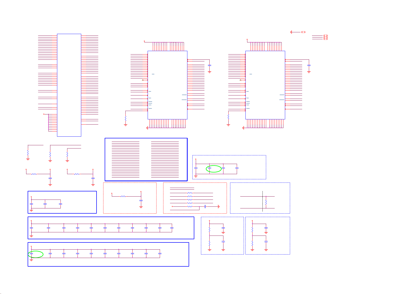
9-4-4 DRR3*2
ARA0
ARA1
ARA2
ARA3
ARA4
ARA5
ARA6
ARA7
ARA8
ARA9
ARA10
ARA11
ARA12
ARA13
ARA14
ARBA0
ARBA1
ARBA2
ARCS
ARCSD
ARRAS#
ARCAS#
ARWE#
ARODT
ARCKE
ARRESET#
ARCLK0
ARCLK0#
DDRVR EF_A1
DDRVR EF_A2
ARTN
MEMTN
MEMTP
DDRV
ARTN
R450
47R 1/16W 5%
R470
AVDD33_DDR
0R05 1/16W
Top Side DRAM#1/2 Bypass Cap
DDRV
C4075
100N 16V
C4080
100N 16V
U401-1
R5
ARA0
AB6
ARA1
W7
ARA2
Y6
ARA3
AC6
ARA4
R7
ARA5
AD6
ARA6
T5
ARA7
Y5
ARA8
U5
ARA9
AC7
ARA10
AA5
ARA11
AC5
ARA12
R6
ARA13
U7
ARA14
AB5
ARBA0
AD5
ARBA1
P6
ARBA2
N2
ARCS
N3
ARCSD
N6
ARRAS
P7
ARCAS
AA6
ARWE
N4
ARODT
U6
ARCKE
V6
ARRESET#
M2
ARCLK
M1
ARCLK#
L3
DDRVREF _A1
AL1
DDRVREF _A2
N8
ARTN
AB12
MEMTN
AA12
MEMTP
AK4
DDRV
AJ5
DDRV
AK5
DDRV
AH6
DDRV
AJ6
DDRV
AG7
DDRV
AH7
DDRV
AF8
DDRV
V9
DDRV
W9
DDRV
U9
DDRV_CKA
MT5802VGEJ
R474
NC/47R 1/16W 5%
C4177
1UF 6.3V
C4079
100N 16V
ARDQM0
ARDQS0
ARDQS0#
ARDQ0
ARDQ1
ARDQ2
ARDQ3
ARDQ4
ARDQ5
ARDQ6
ARDQ7
ARDQM1
ARDQS1
ARDQS1#
ARDQ8
ARDQ9
ARDQ10
ARDQ11
ARDQ12
ARDQ13
ARDQ14
ARDQ15
ARDQM2
ARDQS2
ARDQS2#
ARDQ16
ARDQ17
ARDQ18
ARDQ19
ARDQ20
ARDQ21
ARDQ22
ARDQ23
ARDQM3
ARDQS3
ARDQS3#
ARDQ24
ARDQ25
ARDQ26
ARDQ27
ARDQ28
ARDQ29
ARDQ30
ARDQ31
AVDD10_DDR
AVDD10_DDR
AVDD33_DDR
MEMTP
MEMTN
R473
NC/47R 1/16W 5%
R471
NC/0R05 1/16W
N5
ARDQM0
V1
ARDQS0
V2
ARDQS0#
R2
ARDQ0
AB2
ARDQ1
R1
ARDQ2
AB3
ARDQ3
P1
ARDQ4
AC3
ARDQ5
P3
ARDQ6
AC1
ARDQ7
N7
ARDQM1
W2
ARDQS1
W3
ARDQS1#
Y3
ARDQ8
T3
ARDQ9
AA2
ARDQ10
T2
ARDQ11
Y1
ARDQ12
U1
ARDQ13
AA1
ARDQ14
U3
ARDQ15
AG4
ARDQM2
AH2
ARDQS2
AH3
ARDQS2#
AE3
ARDQ16
AL2
ARDQ17
AE2
ARDQ18
AM1
ARDQ19
AD1
ARDQ20
AM2
ARDQ21
AD2
ARDQ22
AL3
ARDQ23
AF5
ARDQM3
AJ1
ARDQS3
AK3
ARDQS3#
AJ3
ARDQ24
AF3
ARDQ25
AK2
ARDQ26
AF1
ARDQ27
AG5
ARDQ28
AG1
ARDQ29
AK1
ARDQ30
AG2
ARDQ31
AD18
AVDD10_DDR
AD19
AVDD10_DDR
L1
AVDD33_DDR
AVDD10_DDR
DRAM MT41K256M16TW-107-P 4Gb FBGA-96
R421
240R 1%
1_A01_A0
1_A11_A1
1_A21_A2
1_A31_A3
1_A41_A4
1_A51_A5
1_A61_A6
1_A71_A7
1_A81_A8
1_A91_A9
1_A101_A10
1_A111_A11
1_A121_A12
1_A13
1_A14
1_BA01_BA0
1_BA11_BA1
1_BA21_BA2
ARCLK0ARC LK0
ARCLK0#ARCLK0B
1_CKE1_CKE
1_ARCS1_ARC S
1_RAS#1_RAS#
1_CAS#1_CAS#
1_WE#1_WE#
1_RREST_MEM
A_ZQ1
DDRV
N3
A0
P7
A1
P3
A2
N2
A3
P8
A4
P2
A5
R8
A6
R2
A7
T8
A8
R3
A9
L7
A10/AP
R7
A11
N7
A12/BC
T3
A13
T7
A14
M7
NC_A15
M2
BA0
N8
BA1
M3
BA2
J7
CK
K7
CK
K9
CKE
L2
CS
J3
RAS
K3
CAS
L3
WE
T2
RST
L8
ZQ
VSSA9VSSB3VSSE1VSSG8VSSJ2VSSJ8VSSM1VSSM9VSSP1VSSP9VSST1VSST9VSSQB1VSSQB9VSSQD1VSSQD8VSSQE2VSSQE8VSSQF9VSSQG1VSSQ
R9
VDDB2VDDD9VDDG7VDDK2VDDK8VDDN1VDDN9VDDR1VDD
VDDQA1VDDQA8VDDQC1VDDQC9VDDQD2VDDQE9VDDQF1VDDQH2VDDQ
VREF_DQ
VREF_CA
UDQS
UDQS
U402
MT41K256M16TW -107-P
H9
H1
M8
E3
DQ0
F7
DQ1
F2
DQ2
F8
DQ3
H3
DQ4
H8
DQ5
G2
DQ6
H7
DQ7
D7
DQ8
C3
DQ9
C8
DQ10
C2
DQ11
A7
DQ12
A2
DQ13
B8
DQ14
A3
DQ15
F3
LDQS
G3
LDQS
C7
B7
E7
LDM
D3
UDM
K1
ODT
G9
DDR3#1
DDRVREF _A1
A_VREFCA1
ARDQ0
ARDQ1
ARDQ2
ARDQ3
ARDQ4
ARDQ5
ARDQ6
ARDQ7
ARDQ8
ARDQ9
ARDQ10
ARDQ11
ARDQ12
ARDQ13
ARDQ14
ARDQ15
ARDQS0
ARDQS0#
ARDQS1
ARDQS1#
ARDQM0
ARDQM1
1_ODT1_ODT
C4087
100N 16V
2_A02_A0
2_A12_A1
2_A22_A2
2_A32_A3
2_A42_A4
2_A52_A5
2_A62_A6
2_A72_A7
2_A82_A8
2_A92_A9
2_A102_A10
2_A112_A11
2_A122_A12
2_A132_A13
2_A142_A14
2_BA02_BA0
2_BA12_BA1
2_BA22_BA2
ARCLK0ARC LK0
ARCLK0#ARCLK0B
2_CKE2_CKE
2_ARCSD2_ARCSD
2_RAS#2_RAS#
2_CAS#2_CAS#
2_WE#2_WE#
2_RREST_MEM
A_ZQ2
R422
240R 1%
DDRV
VDDB2VDDD9VDDG7VDDK2VDDK8VDDN1VDDN9VDDR1VDD
R9
VDDQA1VDDQA8VDDQC1VDDQC9VDDQD2VDDQE9VDDQF1VDDQH2VDDQ
N3
A0
P7
A1
P3
A2
N2
A3
P8
A4
P2
A5
R8
A6
R2
A7
T8
A8
R3
A9
L7
A10/AP
R7
A11
N7
A12/BC
T3
A13
T7
A14
M7
NC_A15
M2
BA0
N8
BA1
M3
BA2
J7
CK
K7
CK
K9
CKE
L2
CS
J3
RAS
K3
CAS
L3
WE
T2
RST
L8
ZQ
VSSA9VSSB3VSSE1VSSG8VSSJ2VSSJ8VSSM1VSSM9VSSP1VSSP9VSST1VSST9VSSQB1VSSQB9VSSQD1VSSQD8VSSQE2VSSQE8VSSQF9VSSQG1VSSQ
VREF_DQ
VREF_CA
LDQS
LDQS
UDQS
UDQS
DQ10
DQ11
DQ12
DQ13
DQ14
DQ15
UDM
H9
DQ0
DQ1
DQ2
DQ3
DQ4
DQ5
DQ6
DQ7
DQ8
DQ9
LDM
ODT
DDR3#2
U403
MT41K256M16TW-107-P
H1
DDRVREF _A2
M8
E3
F7
F2
F8
H3
H8
G2
H7
D7
C3
C8
C2
A7
A2
B8
A3
F3
G3
C7
B7
E7
D3
K1
G9
CH1 AD/CM
AVDD10_DDR
C4176
NC/1UF 6.3V
2_A10 ARA10
2_A7 ARA7
2_A13 ARA13
2_RREST_MEM ARRESET#
2_A6 ARA6ARA61_A6
2_A8 ARA8
2_A11 ARA11
2_A0 ARA0
2_A5 ARA5
2_RAS# ARR AS#
2_A2 ARA2
2_BA0 ARBA0
2_A3 ARA3
2_WE# ARWE#
ARBA12_BA1
ARA122_A12
ARA42_A4
ARA92_A9
ARA12_A1
ARBA22_BA2
ARA142_A14
DDRVREF _A1 A_VREFC A1
ARCKE 1_CKE
ARODT 1_ODT
DDRV
ARRESET#
DDRV
1_ARCSARCS
2_ARCSDARCSD
R436
NC/0R05 1/16W
R437
NC/0R05 1/16W
R428
47R 1/16W 5%
R448
47R 1/16W 5%
R444
NC/47K +-1% 1/16W
DRAM#1/2 Bottom Layer
C4116
NC/100N 16V
C4111
NC/100N 16V
C4117
NC/100N 16V
A_VREFCA2DD RVREF_A2
2_CKE
2_ODT
C4113
NC/100NF 16V
C4112
NC/100N 16V
Differential Clock
NEAR M ain Chip
ARCLK0
ARCLK0B
NEAR DRAM
ARCLK0ARC LK0
R423
100R 1/16W 1%
ARCLK0B
ARA101_A10
ARBA11_BA1
1_A4 ARA4
1_A7 ARA7
1_RREST_MEM ARRESET#
1_A1 ARA1
1_CAS# ARC AS# 2_CAS# ARC AS#
1_A0 ARA0
AVDD10_DDRAVDD33_DDRD VDD3V3 VCCK
C4185
100N 16V
1_A14 ARA14
1_RAS# ARR AS#
1_A2 ARA2
Reseved only
Place bottom layer and close to U401
VCCK
R465 0R05 1/16W
ARA121_A12
ARA131_A13
ARA91_A9
ARA81_A8
ARA111_A11
ARBA21_BA2
ARA51_A5
ARBA01_BA0
ARA31_A3
ARWE#1_WE#
AVDD10_DDR
GND 4,5,6,8,9,10,11,12, 13,14,15,16,17,18, 19,20,21,22
DDRV
DVDD3V3
VCCK
A_VREFCA2
ARDQ16
ARDQ17
ARDQ18
ARDQ19
ARDQ20
ARDQ21
ARDQ22
ARDQ23
ARDQ24
ARDQ25
ARDQ26
ARDQ27
ARDQ28
ARDQ29
ARDQ30
ARDQ31
ARDQS2
ARDQS2#
ARDQS3
ARDQS3#
ARDQM2
ARDQM3
2_ODT2_ODT
C4088
100N 16V
DDRV 5,8,20
DVDD3V3 5, 6,9,10,11,14, 15,17,18,19,21,22
VCCK 4,5,6 ,19
DDRV
DDRV
C4118
10uF 6.3V
C4100
10uF 6.3V
C4120
NC/10uF 6.3V
C4121
NC/10uF 6.3V
DRAM#1 Bypass Cap
C4053
C4054
100N 16V
100N 16V
DRAM#2 Bypass Cap
C4065
C4063
100N 16V
100N 16V
C4055
100N 16V
C4068
100N 16V
C4119
100N 16V
C4069
100N 16V
C4056
100N 16V
C4070
100N 16V
C4057
100N 16V
C4067
100N 16V
C4058
100N 16V
C4076
100N 16V
C4059
100N 16V
C4091
100N 16V
C4066
100N 16V
DDRV
DDR3#1 Ref Volt.
R424
C4051
1K 1/16W 1%
100N 16V
A_VREFCA1 A_VREFCA2
R426
C4062
1K 1/16W 1%
100N 16V
Near DRAM
DDRV
DDR3#2 Ref Volt.
R425
1K 1/16W 1%
R427
1K 1/16W 1%
C4052
100N 16V
C4064
100N 16V
Near DRAM
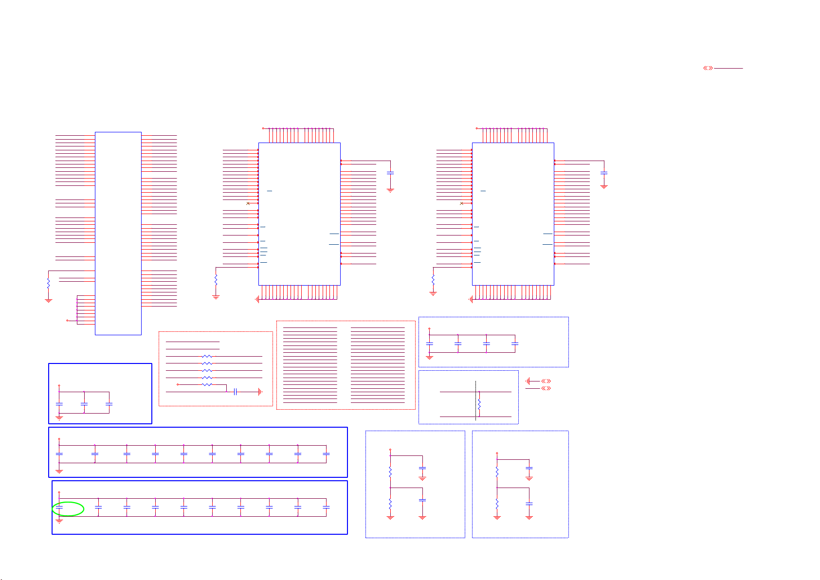
9-4-5 DRR3*2-2
CH2 AD/CM Damping
GND
DDR3#3
GND4,5,6,7,9, 10,11,12,13,14,15, 16,17,18,19,20,21, 22
DDR3#4
DDRV
N3
4_A0
4_A1
4_A2
4_A3
4_A4
4_A5
4_A6
4_A7
4_A8
4_A9
4_A10
4_A11
4_A12
4_A13
4_A14
4_BA0
4_BA1
4_BA2
BRCLK0
BRCLK0#
4_CKE
4_ARCSD
4_RAS#
4_CAS#
4_WE#
4_RREST_MEM
B_ZQ2
R435
240R 1%
A0
VDDB2VDDD9VDDG7VDDK2VDDK8VDDN1VDDN9VDDR1VDD
P7
A1
P3
A2
N2
A3
P8
A4
P2
A5
R8
A6
R2
A7
T8
A8
R3
A9
L7
A10/AP
R7
A11
N7
A12/BC
T3
A13
T7
NC_A14
M7
NC_A15
M2
BA0
N8
BA1
M3
BA2
J7
CK
K7
CK
K9
CKE
L2
J3
K3
L3
T2
L8
NC = J 1,J9,L1,L9
CS
RAS
CAS
WE
RST
ZQ
VSSA9VSSB3VSSE1VSSG8VSSJ2VSSJ8VSSM1VSSM9VSSP1VSSP9VSST1VSST9VSSQB1VSSQB9VSSQD1VSSQD8VSSQE2VSSQE8VSSQF9VSSQG1VSSQ
DRAM#3/4 Bottom Layer
C4109
C4108
NC/100N 16V
NC/100N 16V
Close to DRAM
BRCLK0
BRCLK0#
BRCLK0
R476
100R 1/16W 1%
BRCLK0#
R9
VDDQA1VDDQA8VDDQC1VDDQC9VDDQD2VDDQE9VDDQF1VDDQH2VDDQ
C4107
NC/100N 16V
U405
MT41K128M16JT-107
H9
H1
VREF_DQ
M8
VREF_CA
E3
DQ0
F7
DQ1
F2
DQ2
F8
DQ3
H3
DQ4
H8
DQ5
G2
DQ6
H7
DQ7
D7
DQ8
C3
DQ9
C8
DQ10
C2
DQ11
A7
DQ12
A2
DQ13
B8
DQ14
A3
DQ15
F3
LDQS
G3
LDQS
C7
UDQS
B7
UDQS
E7
LDM
D3
UDM
K1
ODT
G9
GND 4,5,6,7, 9,10,11,12,13,14, 15,16,17,18,19,20, 21,22
DDRV
DDRV 5, 7,20
3_A0
3_A1
3_A2
3_A3
3_A4
3_A5
3_A6
3_A7
3_A8
3_A9
3_A10
3_A11
3_A12
3_A13
3_A14
3_BA0
3_BA1
3_BA2
BRCLK0
BRCLK0#
3_CKE
3_ARCS
3_RAS#
3_CAS#
3_WE#
3_RREST_MEM
B_ZQ1
B_VREFCA2
4_ODT
DDRV
N3
A0
P7
A1
P3
A2
N2
A3
P8
A4
P2
A5
R8
A6
R2
A7
T8
A8
R3
A9
L7
A10/AP
R7
A11
N7
A12/BC
T3
A13
T7
NC_A14
M7
NC_A15
M2
BA0
N8
BA1
M3
BA2
J7
CK
K7
CK
K9
CKE
L2
CS
J3
RAS
K3
CAS
L3
WE
T2
RST
L8
ZQ
VSSA9VSSB3VSSE1VSSG8VSSJ2VSSJ8VSSM1VSSM9VSSP1VSSP9VSST1VSST9VSSQB1VSSQB9VSSQD1VSSQD8VSSQE2VSSQE8VSSQF9VSSQG1VSSQ
R9
VDDB2VDDD9VDDG7VDDK2VDDK8VDDN1VDDN9VDDR1VDD
NC = J 1,J9,L1,L9
3_A2 BRA2
3_BA0 BRBA0
3_A3 BRA3
3_WE# BR WE#
3_A14 BRA14
3_RAS# BRRAS#
3_CAS# BRCAS#
3_BA2 BRBA2
3_A0 BRA0
3_A5 BRA5
3_A6 BRA6
3_A1 BRA1
3_A8 BRA8
3_A11 BRA11
3_A10 BRA10
3_BA1 BRBA1
3_A12 BRA12
3_A4 BRA4
3_A7 BRA7
3_A13 BRA13
3_A9 BRA9
3_RREST_MEM BRR ESET#
VDDQA1VDDQA8VDDQC1VDDQC9VDDQD2VDDQE9VDDQF1VDDQH2VDDQ
VREF_DQ
VREF_CA
DQ10
DQ11
DQ12
DQ13
DQ14
DQ15
LDQS
LDQS
UDQS
UDQS
UDM
H9
DQ0
DQ1
DQ2
DQ3
DQ4
DQ5
DQ6
DQ7
DQ8
DQ9
LDM
ODT
G9
U404
MT41K128M16JT-107
H1
DDRVR EF_B1
M8
B_VREFCA1
E3
BRDQ0
F7
BRDQ1
F2
BRDQ2
F8
BRDQ3
H3
BRDQ4
H8
BRDQ5
G2
BRDQ6
H7
BRDQ7
D7
BRDQ8
C3
BRDQ9
C8
BRDQ10
C2
BRDQ11
A7
BRDQ12
A2
BRDQ13
B8
BRDQ14
A3
BRDQ15
F3
BRDQS0
G3
BRDQS0#
C7
BRDQS1
B7
BRDQS1#
E7
BRDQM0
D3
BRDQM1
K1
3_ODT
4_A2 BRA2
4_BA0 BRBA0
4_A3 BRA3
4_WE# BR WE#
4_A14 BRA14
4_RAS# BRRAS#
4_CAS# BRCAS#
4_BA2 BRBA2
4_A0 BRA0
4_A5 BRA5
4_A6 BRA6
4_A1 BRA1
4_A8 BRA8
4_A11 BRA11
4_A10 BRA10
4_BA1 BRBA1
4_A12 BRA12
4_A4 BRA4
4_A7 BRA7
4_A13 BRA13
4_A9 BRA9
4_RREST_MEM BRR ESET#
C4089
100N 16V
DDR3#4
DDRV
C4071
NC/100N 16V
Damping an d Terminat ion for CLK
Close to M ainChip
U401-2
AH9
BRA0
BRA1
BRA2
BRA3
BRA4
BRA5
BRA6
BRA7
BRA8
BRA9
BRA10
BRA11
BRA12
BRA13
BRA14
BRBA0
BRBA1
BRBA2
BRCS
BRCSD
BRRAS#
BRCAS#
BRWE#
BRODT
BRCKE
BRRESET# BRDQS3
BRCLK0
BRCLK0#
BRTN
DDRVR EF_B1
DDRVR EF_B2
R447
47R 1/16W 5%
DDRV
AH17
AH19
AH11
AG17
AH13
AG21
AH18
AH20
AH16
AH14
AG19
AD10
AJ14
AJ16
AJ19
AJ20
AJ11
AJ13
AJ17
AJ10
AK12
AL23
AE12
AE11
AE10
AE15
AG9
AK9
AK6
AK7
AJ8
AJ7
AM5
AL6
AN2
AE9
AD9
AC9
AB9
BRA0
BRA1
BRA2
BRA3
BRA4
BRA5
BRA6
BRA7
BRA8
BRA9
BRA10
BRA11
BRA12
BRA13
BRA14
BRBA0
BRBA1
BRBA2
BRCS
BRCSD
BRRAS
BRCAS
BRWE
BRODT
BRCKE
BRRESET#
BRCLK
BRCLK#
BRTN
DDRVR EF_B1
DDRVR EF_B2
DDRV
DDRV
DDRV
DDRV
DDRV
DDRV
DDRV
DDRV
DDRV_CKB
MT5802VGEJ
DRAM#3/4 Bypass Cap
DDRV
C4073
C4074
100N 16V
C4078
100N 16V
100N 16V
BRDQM0
BRDQS0
BRDQS0#
BRDQ0
BRDQ1
BRDQ2
BRDQ3
BRDQ4
BRDQ5
BRDQ6
BRDQ7
BRDQM1
BRDQS1
BRDQS1#
BRDQ8
BRDQ9
BRDQ10
BRDQ11
BRDQ12
BRDQ13
BRDQ14
BRDQ15
BRDQM2
BRDQS2
BRDQS2#
BRDQ16
BRDQ17
BRDQ18
BRDQ19
BRDQ20
BRDQ21
BRDQ22
BRDQ23
BRDQM3
BRDQS3
BRDQS3#
BRDQ24
BRDQ25
BRDQ26
BRDQ27
BRDQ28
BRDQ29
BRDQ30
BRDQ31
AM6
BRDQM0
AL9
BRDQS0
AM9
BRDQS0#
AM4
BRDQ0
AM13
BRDQ1
AN4
BRDQ2
AN13
BRDQ3
AM3
BRDQ4
AN14
BRDQ5
AN3
BRDQ6
AL14
BRDQ7
AN5
BRDQM1
AM10
BRDQS1
AN10
BRDQS1#
AN11
BRDQ8
AN7
BRDQ9
AM12
BRDQ10
AM7
BRDQ11
AL11
BRDQ12
AL8
BRDQ13
AL12
BRDQ14
AN8
BRDQ15
AH21
BRDQM2
AM19
BRDQS2
AN19
BRDQS2#
AN16
BRDQ16
AM22
BRDQ17
AM16
BRDQ18
AN22
BRDQ19
AL15
BRDQ20
AM23
BRDQ21
AM15
BRDQ22
AN23
BRDQ23
AK21
BRDQM3
AL20
BRDQS3
AN20
BRDQS3#
AH22
BRDQ24
AN17
BRDQ25
AM21
BRDQ26
AL17
BRDQ27
AJ22
BRDQ28
AL18
BRDQ29
AL21
BRDQ30
AM18
BRDQ31
3_ARCSBRCS
DDRVREF _B1 B_VREF CA1
DDRVREF _B2
BRCKE 3_CKE 4_CKE
DDRV
BRRESET#
4_ARCSDBRCSD
R438 NC/0R05 1/16W
R439 NC/0R05 1/16W
R429 47R 1/16W 5%
3_ODTBRODT
R449 47R 1/16W 5%
R446 NC/47K +-1% 1/16W
DDR3#3
R434
240R 1%
C4114 NC/ 100NF 16V
DDRVR EF_B2
B_VREFCA2
BRDQ16
BRDQ17
BRDQ18
BRDQ19
BRDQ20
BRDQ21
BRDQ22
BRDQ23
BRDQ24
BRDQ25
BRDQ26
BRDQ27
BRDQ28
BRDQ29
BRDQ30
BRDQ31
BRDQS2
BRDQS2#
BRDQS3#
BRDQM2
BRDQM3
4_ODT
C4090
100N 16V
DDRV
DDRV
C4122
10uF 6.3V
C4060
10uF 6.3V
C4125
10uF 6.3V
C4126
10uF 6.3V
DRAM#3 Bypass Cap
C4084
C4097
100N 16V
100N 16V
DRAM#4 Bypass Cap
C4105
C4103
100N 16V
100N 16V
C4102
100N 16V
C4061
100N 16V
C4123
100N 16V
C4101
100N 16V
C4129
100N 16V
C4104
100N 16V
C4081
100N 16V
C4077
100N 16V
C4086
100N 16V
C4106
100N 16V
C4110
100N 16V
C4082
100N 16V
DDR3#3 Ref Volt.
DDRV
R430
1K 1/16W 1%
B_VREFCA1
R433
1K 1/16W 1%
C4194
100N 16V
C4083
100N 16V
DDR3#4 Ref Volt.
DDRV
B_VREFCA2
Near DRAMNear DRAM
R431
1K 1/16W 1 %
R432
1K 1/16W 1%
C4181
100N 16V
C4096
100N 16V
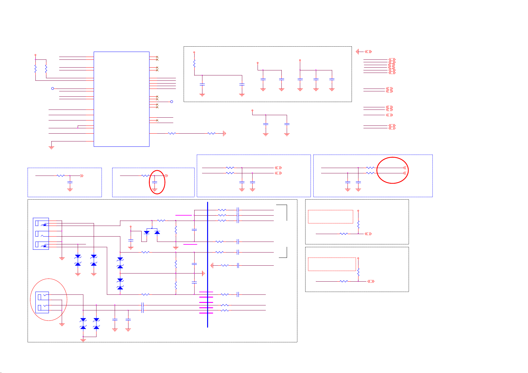
9-4-6 YPbPr/CVBS/SPIDIF
DVDD3V3
R164
1K2 OHM
Tun er/DEMOD
TP109
Close to Main Chip
IF_AGC
R161
1K2 OHM
AVDD33_VIDEO_STB
AVDD33_DEMOD_STB
AVDD33_DTMB
DVDD1V2_DTMB
AVDD1V2_DTMB
AVSS33_DEMOD
R166
10K 1/16W 5%
ADCIN P_DEMOD
ADCIN N_DEMOD
IF_AGC
RF_AGC
OSCL2
OSDA2
DISEQC_I N
DISEQC_OU T
DVBS2_SIF_I P
DVBS2_SIF_QP
C120
47NF 16V
IF_AGCT 13
U401-5
A31
ADCIN P_DEMOD
B31
ADCIN N_DEMOD
C9
IF_AGC
D9
RF_AGC
E14
OSCL2
F14
OSDA2
D31
DISEQC_I N
D30
DISEQC_OU T
B33
DVBS2_SIFI P
B32
DVBS2_SIFQP
J24
AVDD33_VID EO_STB
J25
AVDD33_DEMOD_STB
L20
AVDD33_DEMODE
AM24
DVDD12_D EMODE
AN24
DVDD12_D EMODE
AJ23
AVDD12_DEMODE
L22
AVSS33_DEMOD
MT5802VGEJ
RF_AGC
TP_H
TP_V
U1TX
U1RX
SOY0
COM0
PB0P
PR0P
SOY1
COM1
PB1P
PR1P
CVBS0P
CVBS1P
CVBS_COM
VDACX_OUT
R168
10K 1/16W 5%
3V3SB
H31
J32
K32
J31
F31
SOY0
F32
E31
E32
E33
H32
H33
G31
G33
G32
C33
D32
C32
E30
Y0P
COM0
PB0P
PR0P
CVBS0P
CVBS_COM
R5168
10R 1/16W 5%
TP108
TUNER_BY PASS_OUT
Y0P
Y1P
Analog Power
R478
0R05 1/16W
AVDD33_VIDEO_STB
C4156
10uF 6.3V
R1004
NC/75 OHM +-5% 1/16W
AVDD33_DEMOD_STB
C4191
NC/100N 16V
AVDD1V2
AVDD3V3
AVDD33_DTMB
C4197
NC/10N 50V
DVDD1V2_D TMB
C4196
100N 16V
C4179
100N 16V
C4195
10UF 6. 3V 20%
AVDD1V2
AVDD1V2_DTMB
C4188
NC/10N 50V
C4198
100N 16V
C4189
10UF 6. 3V 20%
Close to Main Chi p
C133
100N 16V
RF_AGCS 13
ADCIN P_DEMOD
Close to Mai n Chip
R126
R128
0R05 1/16W
0R05 1/16W
C1046
NC/47pF 50V
TU_FAT_IN2+
TU_FAT_IN2-ADCIN N_DEMOD
C1047
NC/47pF 50V
TU_FAT_IN2+ 13
TU_FAT_IN2- 13
DVBS2_SIF_I P
DVBS2_SIF_QP
Close to Mai n Chip
C1049
NC/47pF 50V
0103 Update
GND 4,5, 6,7,8,10,11, 12,13,14,15,16,17,1 8,19,20,21,22
C1048
AVDD3V3
3V3SB
+5V_SW
+5V_STB
AVDD1V2
DVDD3V3
DISEQC_OU T
R129
R130
0R05 1/16W
0R05 1/16W
NC/47pF 50V
AL1O
AR1O
OSCL2
OSDA2
AIN_R0
AIN_L0
AVDD3V3 5,11,1 2,18,21
3V3SB 4,5,6,12,16, 18,22
+5V_SW 4,5,12,13, 15,21,22
+5V_STB 4,5,12,16
AVDD1V2 5
DVDD3V3 5,6,7, 10,11,14,15,17,18,1 9,21,22
AL1O 21,22
AR1O 21,22
OSCL2 10
OSDA2 10
DISEQC_OUT 14
AIN_R0 21
AIN_L0 21
DVBS2_SIFIP 13
DVBS2_SIFQP 13
Rear YPbPr /CVBS + R/L
RCA 8P
C
B
A
CN101
CN102
A
B
CONN
6
7
8
4
5
1
2
3
2
1
4
3
11/23 exchange
Y_DET
Y_IN _1
PB_IN_1
YPBPR_D ETECT
PR_IN_1
12
ZD101
NC/AZ 5123-01H
YPbPrL_IN
YPbPrR_I N
12
ZD105
wi th GND
R1013 0R05 1/10W
+5V_STB
C109
1uF 10V
12
ZD106
NC/AZ 5123-01H
12
ZD104
NC/AZ 5123-01H
12
ZD102
NC/AZ 5123-01H
12
ZD103
NC/AZ 5123-01H
C1045
C1044
NC/AZ 5123-01H
1N 50V
1N 50V
3
D101
R1005
NC/BAV99
1
2
R1008
0R05 1/10W
R1012
0R05 1/10W
C1029 1uF 10V R1139 30K OHM +-1% 1/16W
C1030 1uF 10V
75R 1/16W 1%
wi th GND
R1010
75R 1/16W 1%
R1011
75R 1/16W 1%
wi th GND
wi th GND
wi th GND
NEAR YPbPr CONNECTOR
C1034
10PF 50V
C1040
10PF 50V
C1041
10PF 50V
R1001
10R 1/16W 1%
R1002
100R 1/16W 5%
R1003
100R 1/16W 5%
R1007
100R 1/16W 5%
R1009
100R 1/16W 5%
R104
0R05 1/16W
CVBS_COM
wi th GND
R1015
100R 1/16W 5%
wi th GND
R1140 30K OH M +-1% 1/16W
Near Scaler
C1035
1.5nF 50V
C1036
47nF 16V
C1037
10N 50V
C1038
10N 50V
C1039
10N 50V
C1031
1uF 10V
ゲ斗 猽
C1042
10N 50V
SOY0
CVBS0P
Y0P
COM0
PB0P
CVBS_COM
CVBS3PǐCN116
PR0P
AIN_R0
AIN_L0
ǐ
キ︽絬
Source_DET
H:Pr Plug-in (YPbPr)
L:Pr Plug-out (AV)
YPBPR_D ETECT
Vedio_DET
H:Pr Plug-in (Cable detect)
L:Pr Plug-out (Non Cable)
Y_DET
R1016
100R 1/16W 5%
R114
100R 1/16W 5%
DVDD3V3
DVDD3V3
R1017
47K 1/16W 5%
YPBPR_D ETECT1 17
R106
47K 1/16W 5%
VIDEO_DET 17

9-4-7 AUDIO AMP
8x10. 2mm (獶IO跋)
AD87588-LG48NAY:356G0616048163
AD83586B-LG48NAY:356G0616048602
2.0 CH
INDUCTOR
24V
10uH
AD82588
073G253S 81 Y
12V
15uH
AD83586
373G253S247Y00
2.1 CH
22uH
AD83586
373G253S147Y00
AMP_CFG0
AMP_CFG1
R615 N C/0R05 OHM
R616 0R0 5 1/10W
AU_VDD3V3
SDI AMP_SA0
LRCLKI
BICKI
MCLK
HEAT SINK
AU_12V
DVDD 3V3
1 2
1
2
FB601
120R 6A
FB602
120R 3A
HS601
C627
100N 16V
12
C609
C610
100N 50V
100N 50V
LA
LB
45LA46
47NC48
U601
GNDL
VDDLA
49
THERMALPAD
1
SDATA1
2
MS
3
PLL
4
CFG0
5
CFG1
6
CLK_OUT
7
DGND
8
9
10
11
12
PVDD
AU_VDD3V3
C602
10UF 6. 3V 20%
AD82588B-LG48NAY
DVDD
SDATA0
LRCIN
BCLK
MCLK
NC13NC14NC15NC16NC17NC18NC19NC20NC21NC22NC23NC
DVDD3V3
R601
0R05 1/16W
R604
NC/0R 05 OHM
C611
100N 50V
RB
42
43LB44
VDDLB
VDDRB
R602
NC/0R 05 1/16W
AMP_CFG0
AMP_CFG1
R605
0R05 1/16W
40RB41
GNDR
C612
100N 50V
RA
LINEI N
LREX
RESET#
ERROR#
DVDD
DGND
DEF
SDA
38RA39
VDDRA
PD#
SA1
SA0
SCL
24
PVDD
For EMI, close to SoC
All Path Grounding(20mil)
AOMCLK
AOBCK
AOLRCK
AOSDATA0
RA
RB
LA
LB
CFG0
0
10
01
1
R643
0R05 1/16W
R603
0R05 1/16W
R606
0R05 1/16W
R607
0R05 1/16W
C616
470pF 50V
R611
10 OHM
R613
10 OHM
C623
470pF 50V
C630
470pF 50V
R622
10 OHM
R627
10 OHM
C642
470pF 50V
Mode
Reserved
2.1CH
Stereo
Mono
R634 0R 05
+
C614
C625
100N 16V
PVDD
RESET#
AMP_DEF
AMP_SA1
C632
100P 50V
Anti-pop
R645
NC/470K
1
R640
180K
R608
10K 1/4W
R617
0R05 1/10W
R620
R621
C633
22R 1/10W 5%
100P 50V
22R 1/10W 5%
DVDD 3V3
R649
NC/1K
23
Q603
NC/LMBT3906LT1G
R639
0R05 1/16W
AU_VDD3V3
150uF 20% 16V
37
NC
36
35
34
33
32
31
30
29
28
27
26
A_SCL
25
A_SDA
Option
OSCL2
OSDA2
DVDD3V3
I2SAMP_RESET
Low: reset
High: normal
Reset (pull -up)
I2SAMP_RESETPWRDN
C626
22UF
I2C address
Write=0110"SA0"0"SA1"0=0x60
AMP_SA0
AMP_SA1
AMP_PWRDN17
R632
10K 1/16W 5%
R636
10K 1/16W 5%
Q601
NC/MMBT3904
R610
0R05 1/16W
R625
R624
NC/10K
NC/10K
R629
R630
10K 1/16W 5%
R633
0R05 1/16W
R644
NC/ 0R05 1/16W
DVDD3V3D VDD3V3
10K 1/16W 5%
DVDD 3V3
R660
NC/ 10K 1/16W 5%
C619
R609
10K 1/16W 5%
1uF 10V
R626
NC/10K 1/16W 5%
AMP_DEF
R631
10K 1/16W 5%
PWRDN
R635
10K 1/16W 5%
Mo dify by EM I
RESET#
CFG1
0
1
MCLK
C603
33P 50V
BICKI
C605
33P 50V
LRCLKI
C607
33P 50V
SDI
C608
33P 50V
R637 0R0 5
R638 0R0 5
R642 0R0 5
Ground ing
Ground ing
Ground ing
Ground ing
L601
22uH
R612
10 OHM
R614
10 OHM
L602
22uH
L603
22uH
R623
10 OHM
R628
10 OHM
L604
22uH
GND 4,5, 6,7,8,9,11, 12,13,14,15,16,17, 18,19,20,21,22
3V3SB
DVDD3V3
+5V_SW
AU_12V
GPIO & I2C Control
OSDA2
OSCL2
I2SAMP_RESET
I2S Control
AOMCLK21
AOBCK21
AOLRCK21
AOSDATA021
PWRDN
C615
100N 50V
C618
220N 50V
C620
100N 50V
C621
220N 50V
C624
100N 50V
C629
100N 50V
C634
220N 50V
C635
100N 50V
C640
220N 50V
C643
100N 50V
3V3SB 4,5, 6,9,12,16,18,22
DVDD3V3 5,6,7,9,11,14,15 ,17,18,19,21,22
+5V_SW 4,5, 12,13,15,21,22
AU_12V 5
OSDA2 9
OSCL2 9
I2SAMP_RESET 17
AOMCLK
AOBCK
AOLRCK
AOSDATA0
PWRDN 22
C617
100N 50V
C622
100N 50V
C631
100N 50V
C641
100N 50V
Stereo mode:
FB607, FB610,
C628: NC
56
1
R-
2
R+
3
L-
4
L+
CN601
CONN
4 ohm: 10uH, 470nF
6 ohm: 15uH, 470nF
8 ohm: 22uH, 470nF
R
RR+
LL+
L
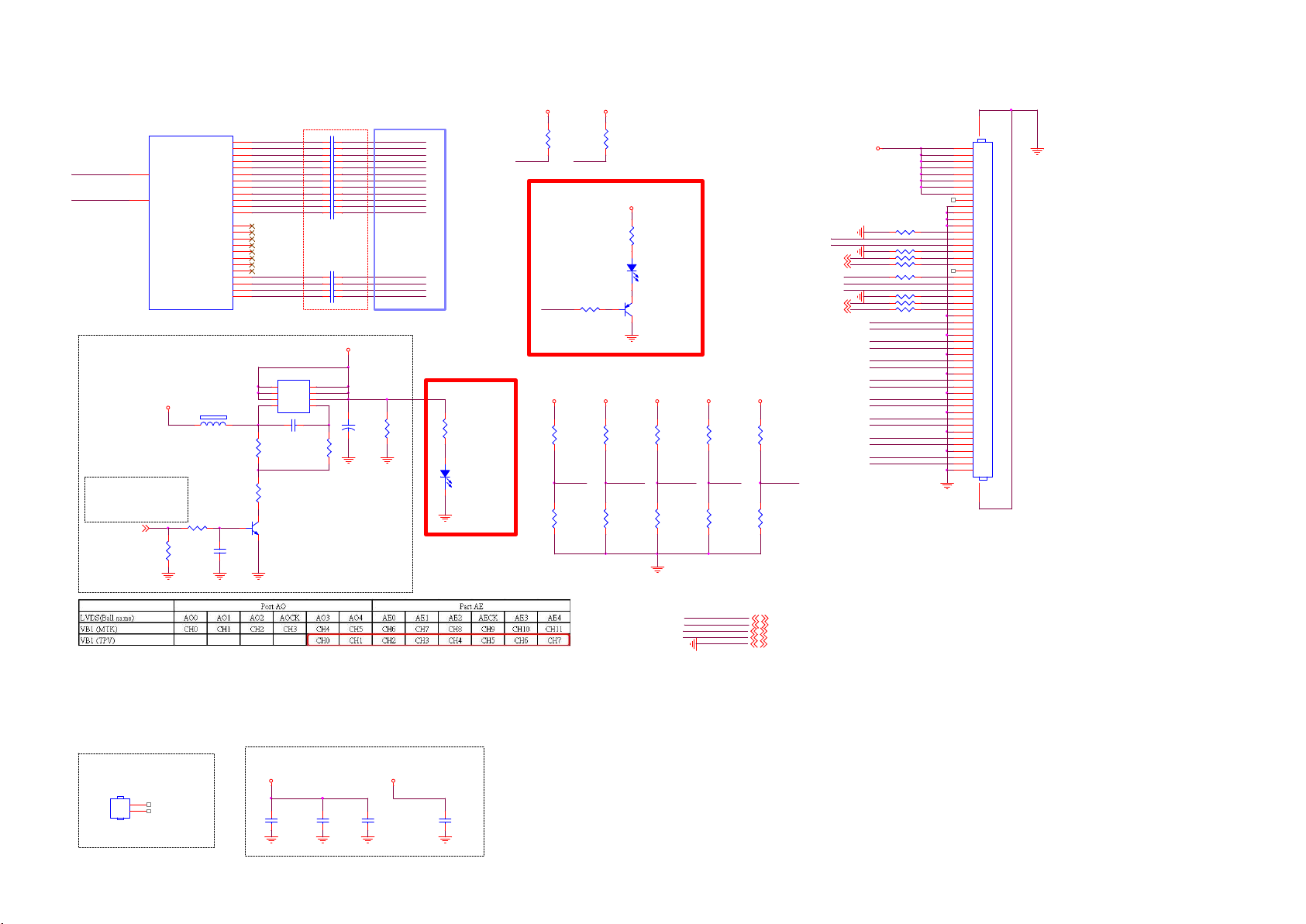
9-4-8 VB1 output
MT5802 Vx1 OUTPUT
U401-3
AVDD10_LVDS_STB
AVDD33_LVDSA
AH23
K20
MT5802VGEJ
AVDD10_LVDS_STB
AVDD33_LVDSA
Panel VCC=12V
18V_12V
PANEL_PWR_EN
Normal:High
Stand_By:Low
PANEL_PWR_EN17
FB712
1 2
120R 6A
R799
10K 1/16W 5%
R788
10K 1/16W 5 %
AE0P
AE0N
AE1P
AE1N
AE2P
AE2N
AECKP
AECKN
AE3P
AE3N
AE4P
AE4N
AO0P
AO0N
AO1P
AO1N
AO2P
AO2N
AOCKP
AOCKN
AO3P
AO3N
AO4P
AO4N
10K 1/10W 5%
C791
NC/4. 7UF 10V
AN28
AM28
AL27
AK27
AL26
AK26
AN26
AM26
AL25
AK25
AL24
AK24
AN32
AM32
AL31
AK31
AL30
AK30
AN30
AM30
AL29
AK29
AL28
AK28
R793
Close to SoC
LVDSTX_AE0P
LVDSTX_AE0N
LVDSTX_AE1P
LVDSTX_AE1N
LVDSTX_AE2P
LVDSTX_AE2N
LVDSTX_AECKP
LVDSTX_AECKN
LVDSTX_AE3P
LVDSTX_AE3N
LVDSTX_AE4P
LVDSTX_AE4N
LVDSTX_AO3P
LVDSTX_AO3N
LVDSTX_AO4P
LVDSTX_AO4N
Q784
AON4421
8
D
D
7
D
D
6
D
D
5
G4S
C788
1UF 10% 16V
6K8 1/10W 5 %
R785
5.1KOHM +-5% 1/10W
Q785
BC847N3
C4939 100N 16V
C4940 100N 16V
C4941 100N 16V
C4942 100N 16V
C4943 100N 16V
C4944 100N 16V
C4945 100N 16V
C4946 100N 16V
C4947 100N 16V
C4948 100N 16V
C4949 100N 16V
C4950 100N 16V
C4959 100N 16V
C4960 100N 16V
C4961 100N 16V
C4962 100N 16V
Panel_12V
1
2
3
+
R797
C789
220UF 16V
To CN408
SOC-VB1-TX2p
SOC-VB1-TX2n
SOC-VB1-TX3p
SOC-VB1-TX3n
SOC-VB1-TX4p
SOC-VB1-TX4n
SOC-VB1-TX5p
SOC-VB1-TX5n
SOC-VB1-TX6p
SOC-VB1-TX6n
SOC-VB1-TX7p
SOC-VB1-TX7n
SOC-VB1-TX0p
SOC-VB1-TX0n
SOC-VB1-TX1p
SOC-VB1-TX1n
R4740
4.7K
10/13 Add
R303
NC/5 .1KOHM +-5% 1/10W
12
LED301
NC/G PTS06033GC1-PB
HTPDn
DVDD3V3
10/13 Add
LOCKn
R4969
10K 1/16W 5%
LOCKn
R301
NC/750R 1/16W 5%
R1036
NC/10K+-5%1/16W
AGP
R1035
NC/1 0K 1/16W 5%
DVDD3V3
R4968
10K 1/16W 5%
DVDD3V3
DVDD3V3DVDD3V3
R1043
NC/10K+-5%1/16W
Panel inte rnal use
R1037
NC/1 0K 1/16W 5%
R302
NC/470R 1/16W 5%
12
LED302
NC/G PTS06033GC1-PB
Q301
NC/BC 857C
DVDD3V3
R1038
NC/10K 1/16W 5%
D_Fomat 1 Bit_SELD _Fomat0
Panel inte rnal use
R1042
NC/10K+-5%1/16W
DVDD3V3
R1019
NC/10K 1/16W 5%
R1040
NC/10K+-5%1/16W
H or NC = 10bit
L = 8bi t
DVDD3V3
R1020
R3208
NC/10K 1/16W 5%
LD_EN
Data fo rmat
L :Non division ,
NC/0R 05 1/16W
ˉH: 2 di vision
Panel_12V
R3202 NC/0R05 1/16W
D_Fomat 0
D_Fomat 1
R3215 NC/0R05 1/16W
OSDA06
OSCL06
HTPDn21
LOCKn17
R3204 NC/0R05 1/16W
R3205 NC/0R05 1/16W
Bit_SEL
R3207 NC/0R05 1/16W
LD_EN
AGP
R3219 0R05 1/16W
HTPDn
R3209 0R05 1/16W
LOCKn
R3210 0R05 1/16W
SOC-VB1-TX0n
SOC-VB1-TX0p
SOC-VB1-TX1n
SOC-VB1-TX1p
SOC-VB1-TX2n
SOC-VB1-TX2p
SOC-VB1-TX3n
SOC-VB1-TX3p
SOC-VB1-TX4n
SOC-VB1-TX4p
SOC-VB1-TX5n
SOC-VB1-TX5p
SOC-VB1-TX6n
SOC-VB1-TX6p
SOC-VB1-TX7n
SOC-VB1-TX7p
51
50
49
48
47
46
45
44
43
42
41
40
39
38
37
36
35
34
33
32
31
30
29
28
27
26
25
24
23
22
21
20
19
18
17
16
15
14
13
12
11
10
9
8
7
6
5
4
3
2
1
52 53
CN408
CONN 51P
MT5802 HEAT SINK
HS401
HEAT SINK
1
2
X90G401004200000BF
Analog Power
AVDD3V3AVDD1V0_1
AVDD10_LVDS_STB AVDD33_LVDSA
C4163
C4187
10UF 6. 3V 20%
1uF 10V
C4164
100N 16V
C4190
100N 16V
AVDD3V3
DVDD3V3
AVDD1V0_1
18V_12V
AVDD3V3 5,9,12, 18,21
DVDD3V3 5,6,7,9,1 0,14,15,17,18,19,2 1,22
AVDD1V0_1 5,12
18V_12V 4,5,14,22
GND 4,5,6, 7,8,9,10,12, 13,14,15,16,17,18, 19,20,21,22

9-4-9 HDMI/MHL
TMDSD2+
DSHLD0
TMDSD2-
TMDSD1+
DSHLD1
TMDSD1-
TMDSD0+
DSHLD2
TMDSD0-
TMDSC+
CSHLD0
TMDSC-
DDC_GND
VCC5
U401-6
G17
HDMI_CEC_1
E18
MHL_SENSE
F18
HDMI_0_PWR5V
D18
HDMI_0_HPD_CBU S
E19
HDMI_0_SCL
F19
HDMI_0_SDA
F23
HDMI_1_PWR5V
F21
HDMI_1_HPD
G19
HDMI_1_SCL
G21
HDMI_1_SDA
E23
HDMI_2_PWR5V
F22
HDMI_2_HPD
E22
HDMI_2_SCL
E21
HDMI_2_SDA
E27
AVDD10_ECBUS_STB
B17
AVDD10_HDMI_STB
K24
AVDD33_ECBUS_STB
J19
AVDD33_HDMI
J20
AVDD33_HDMI
MT5802VGEJ
кで皌
1
2
3
4
5
6
7
8
9
10
11
12
13
CEC
14
NC
15
SCL
SDA
HPD
SCL0
16
SDA0
17
18
OPWR0_5V
19
ECBUS Impedance: 35<Z<57.5ohm
+5V_SW
+5V_USB
MHL_PWR_EN
A15
B15
C14
D14
A13
B13
C16
D16
B20
A20
C19
D19
B18
A18
D21
C21
B24
A24
D23
C23
B22
A22
D25
C25
稼﹊
MHL_SENSE
RX_0_2
RX_0_2B
RX_0_1
RX_0_1B
RX_0_0
RX_0_0B
RX_0_C
RX_0_CB
R509 22R 1/16W 5%
R521 4.7R
U501
2
1
G529A1TB1U
C509
10UF 10V
RX_0_0
RX_0_0B
RX_0_1
RX_0_1B
RX_0_2
RX_0_2B
RX_0_C
RX_0_CB
RX_1_0
RX_1_0B
RX_1_1
RX_1_1B
RX_1_2
RX_1_2B
RX_1_C
RX_1_CB
RX_2_0
RX_2_0B
RX_2_1
RX_2_1B
RX_2_2
RX_2_2B
RX_2_C
RX_2_CB
OPWR0_5V
IN3OUT
GND
EN
OUT
OC
HDMI_0_RX_0
HDMI_0_RX_0B
HDMI_0_RX_1
HDMI_0_RX_1B
HDMI_0_RX_2
HDMI_0_RX_2B
HDMI_0_RX_C
HDMI_0_RX_CB
HDMI_1_RX_0
HDMI_1_RX_0B
HDMI_1_RX_1
HDMI_1_RX_1B
HDMI_1_RX_2
HDMI_1_RX_2B
HDMI_1_RX_C
HDMI_1_RX_CB
HDMI_2_RX_0
HDMI_2_RX_0B
HDMI_2_RX_1
HDMI_2_RX_1B
HDMI_2_RX_2
HDMI_2_RX_2B
HDMI_2_RX_C
HDMI_2_RX_CB
90
R519 47R 1/ 16W 5%
R5404.7R
R5414.7R
R5424.7R
R5434.7R
R5444.7R
R5454.7R
R5464.7R
R5474.7R
HDMI_CEC_0
R515 100R 1/ 16W 5%
R516 100R 1/ 16W 5%
FB502
12
NC/120R 3A
FB501
12
120R 3A
R512
100K 1/16W 5% R511
R501
HDMI_CEC CEC
100R 1/16W 5%
MHL_SENSE
HDMI_0_PWR5V
HDMI_0_HPD_CB US
HDMI_0_SCL
HDMI_0_SDA
HDMI_1_PWR5V
HDMI_1_HPD
HDMI_1_SCL
HDMI_1_SDA
HDMI_2_PWR5V
HDMI_2_HPD
HDMI_2_SCL
HDMI_2_SDA
AVDD10_ECBUS_STB
AVDD10_HDMI_STB
AVDD33_ECBUS_STB
AVDD33_HDMI
AVDD33_HDMI
Side HDMI/MHL Port 1 (HDMI 2.0 / MHL)
388G340FJ05FAT0001: BPR 1.6mm
CN501
20
SHLD0
22
SHLD2
23
SHLD3
21
SHLD1
HDMI 19P
Side HDMI port 2 (HDMI 2.0 & HDCP 2.2)
CN502
20
22
23
21
SHLD0
SHLD2
SHLD3
SHLD1
HDMI 19P
TMDSD2+
DSHLD0
TMDSD2-
TMDSD1+
DSHLD1
TMDSD1-
TMDSD0+
DSHLD2
TMDSD0-
TMDSC+
CSHLD0
TMDSC-
DDC_GND
VCC5
1
2
3
4
5
6
7
8
9
10
11
12
13
CEC
14
NC
15
SCL
16
SDA
17
18
19
HPD
8/20 modify
388G340FJ05FAT0001: BPR 1.6mm
кで皌
SCL1
SDA1
OPWR1_5V
90
R5484.7R
R5494.7R
R5514.7R
R5504.7R
R5544.7R
R5524.7R
R5564.7R
R5554.7R
POH_HPD1
R571
100K 1/16W 5 %
稼﹊
RX_1_2
RX_1_2B
RX_1_1
RX_1_1B
RX_1_0
RX_1_0B
RX_1_C
RX_1_CB
HDMI_CEC_1
R564100R 1/16W 5%
R565100R 1/16W 5%
R572 1K 1/ 16W 5%
R569
1K 1/16W 5%
R570 1K 1/16W 5%
Q507
BC847N3
HDMI_1_HPD
R566
47K 1/16W 5%
HDMI_1_PWR5V
1
R513
4
5
6
R568
4.7K1/16W
3
USB_MHL_OC
+5V_STB
2
D506
LBAT54CLT1G
R514
47K 1/16W 5%
47K 1/16W 5%
HDMI_0_PWR5V
HDMI_0_HPD_CBU S
OPWR1_5V
R567
47K 1/16W 5%
Analog Power
AVDD3V3_HDMI
+5V_SW
R553
1K 1/16W 5%
CEC
with GND
HDMI_CEC
C506
6.8PF 50V
USB_MHL_OC
MHL_SENSE
R522
300K
HDMI_0_SCL
HDMI_0_SDA
C510
10UF 10V
HDMI_1_SCL
HDMI_1_SDA
AVDD33_HDMI
Q509
AO3414
C4174
C501
NC/10NF 50V
R506
100K 1/16W 5%
R505 0R05 1 /16W
R504 0R05 1 /16W
R503 0R05 1 /16W
3V3SB
R510
10K 1/16W 5%
10K 1/16W 5%
100N 16V
Prevent HDMI leakage from HDMI device.
HDMI_CEC_0
HDMI_CEC_1
HDMI_CEC_2
AVDD1V0_1
AVDD10_HDMI_STB
C4192
C4180
100N 16V
100N 16V
Bottom HDMI port 3 ( ARC / HDMI 1.4 )
20
22
23
21
AVDD3V3
CN503
SHLD0
SHLD2
SHLD3
SHLD1
HDMI 19P
AVDD1V0_STB
AVDD10_ECBUS_STB
C4178
1UF 6. 3V
R507 0R05 1/ 16W
кで皌
1
TMDSD2+
2
DSHLD0
3
TMDSD2-
4
TMDSD1+
5
DSHLD1
6
TMDSD1-
7
TMDSD0+
8
DSHLD2
9
TMDSD0-
10
TMDSC+
11
CSHLD0
12
TMDSC-
13
CEC
14
NC
15
SCL2
SCL
16
SDA2
SDA
17
DDC_GND
18
VCC5
+5V_USB
+5V_STB
+5V_SW
3V3SB
AVDD3V3
DVDD3V3
AVDD1V0_STB
AVDD1V0_1
MHL_PWR_EN
USB_MHL_OC
OPWR2_5V
19
POH_HPD2
HPD
+5V_USB 18
+5V_STB 4,5,9,16
+5V_SW 4,5,13, 15,21,22
3V3SB 4,5,6,9, 16,18,22
AVDD3V3 5,9,11,18,21
DVDD3V3 5, 6,7,9,10,11, 14,15,17,18,19,21,2 2
AVDD1V0_STB 5,6,18
AVDD1V0_1 5,11
MHL_PWR_EN 17
USB_MHL_OC 17
GND 4,5,6,7,8,9,10,11, 13,14,15,16,17,18,1 9,20,21,22
3V3SB
AVDD33_ECBUS_STB
C4183
10UF
AVDD3V3_HDMI
90
R5574.7R
R5584.7R
R5594.7R
R5604.7R
R5614.7R
R5624.7R
R5634.7R
R5734.7R
HDMI_CEC_2
ARC_HDMI
R538 100R 1/ 16W 5%
R539 100R 1/ 16W 5%
R588
100K 1/16W 5%
C4155
100N 16V
稼﹊
RX_2_2
RX_2_2B
RX_2_1
RX_2_1B
RX_2_0
RX_2_0B
RX_2_C
RX_2_CB
R574 1K 1/1 6W 5%
R575
1K 1/16W 5%
R576 1K 1/ 16W 5%
Q508
BC847N3
Audio Return Channel (ARC)
ARC_HDMI
+5V_SW
R577
47K 1/16W 5%
R579
47K 1/16W 5%
C505
1uF 10V
Close to connector
OPWR2_5V
R537
R536
47K 1/16W 5%
47K 1/16W 5%
HDMI_2_SCL
HDMI_2_SDA
HDMI_2_PWR5V
R580
4.7K1/16W
HDMI_2_HPD
from Scaler ARC
R530
180R
R529
with GND
82R
U506
1
RX_0_2
CH1
NC
2
RX_0_2B
CH2
NC
3
GND
VN
VN
4
RX_0_1
CH3
NC
RX_0_1B
CH45NC
NC/TVU1240R1A
U507
1
RX_0_0 RX_0_0
CH1
NC
2
RX_0_0B
CH2
NC
3
GND
VN
VN
4
RX_0_C
CH3
RX_0_CB
HDMI_CEC_0
SCL0
SDA0
Close to connector
HDMI_CEC_1
SCL1
SDA1
OPWR1_5V
Close to connector
HDMI_CEC_2
SCL2
SDA2
OPWR2_5V
NC
CH45NC
NC/TVU1240R1A
U508
1
CH1
NC
2
CH2
NC
3
VN
4
CH3
NC
CH45NC
NC/TVU1240R1A
U516
1
RX_1_2
CH1
NC
2
RX_1_2B
CH2
NC
3
GND
VN
4
RX_1_1
CH3
CH45NC
NC/TVU1240R1A
U517
1
CH1
2
CH2
3
VN
4
CH3
CH45NC
NC/TVU1240R1A
U518
1
CH1
2
CH2
3
VN
4
CH3
CH45NC
NC/TVU1240R1A
U509
1
CH1
2
CH2
3
VN
4
CH3
CH45NC
NC/TVU1240R1A
U510
1
CH1
2
CH2
3
VN
4
CH3
CH45NC
NC/TVU1240R1A
U511
1
CH1
2
CH2
3
VN
4
CH3
CH45NC
NC/TVU1240R1A
NC
NC
NC
NC
NC
NC
NC
NC
NC
NC
RX_1_1B
RX_1_0
RX_1_0B
GND
RX_1_C
RX_1_CB R X_1_CB
RX_2_2
RX_2_2B
GND
RX_2_1
RX_2_1B
RX_2_0
RX_2_0B
GND
RX_2_C
RX_2_CB R X_2_CB
ARC 21
10
RX_0_2
9
RX_0_2B
8
7
RX_0_1
6
RX_0_1B
10
9
RX_0_0B
8
7
RX_0_C
6
RX_0_CB
10
9
8
VN
7
6
OPWR0_5VOPWR0_5V
10
RX_1_2
9
RX_1_2B
8
VN
7
RX_1_1
6
RX_1_1B
10
RX_1_0
9
RX_1_0B
8
VN
7
RX_1_C
6
10
NC
9
NC
8
VN
7
NC
6
10
RX_2_2
9
RX_2_2B
8
VN
7
RX_2_1
6
RX_2_1B
10
RX_2_0
9
RX_2_0B
8
VN
7
RX_2_C
6
10
NC
9
NC
8
VN
7
NC
6
HDMI_CEC_0
SCL0
SDA0
HDMI_CEC_1
SCL1
SDA1
OPWR1_5V
HDMI_CEC_2
SCL2
SDA2
OPWR2_5V
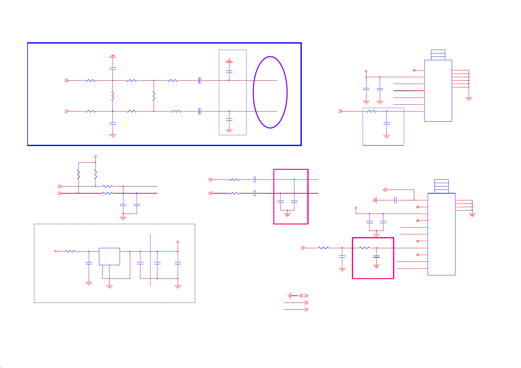
9-4-10 Tuner
TU_FAT_IN2+9
TU_FAT_IN2-9
Di ffe renti al Pa ir
OSDA16
OSCL16
+5V_SW TO TUNER3.3V
R102
+5V_SW
0R05 1/ 8W
R122
0R05 1/ 16W
R123
0R05 1/ 16W
TUNER3.3V
R178
1K2 OHM
C106
1UF 10% 16V
R177
1K2 OHM
R167
R176
22R 1/ 16W 5%
22R 1/ 16W 5%
U102
G960T63Uf
3
VIN
4
VOUT
GND14
C149
NC/ 22N 25V
R120
0R05 1/ 16W
R125
NC/ 620R
R121
0R05 1/ 16W
C150
NC/ 22N 25V
C121
100P 50V
2
TUN_SDA
TUN_SCL
C122
100P 50V
C103
10UF 6.3V 20%
0R05 1/ 16W
R124
NC/ 620R
0R05 1/ 16W
C104
1UF 10% 16V
R115
R116
TUNER3. 3V
C105
100N 16V
T2 TUNER
C147
100N 50V
C148
100N 50V
C110
33P 50V
C113
33P 50V
Closed to T uner
IF PATH
TUNER
IF_P_TU
IF_N _TU
TUNER3.3V
TUN_SDA
C124
C123
10UF 6.3V
IF_AGC T9
IF_AGC T
R187
10K 1%
100N 16V
C119
47NF 16V
TUN_SCL
IF_N_TU
IF_P_TU
IF_AGC_T
Closed to T uner
1
Ant. PWR
2
+B1(+3.3V)
3
SDA
4
SCL
5
DIF (N)
6
DIF (P)
7
IF AGC
ST42CS-2-E
Device Address : 0xC0
3V3: TYP: 180mA, Max: 230mA
TH1
TH2
TH3
TH4
TH5
TH6
TDSY-G480D
TU101
8
9
10
11
12
13
S2 TUNER
C126
10PF 50V
IP
QP
R133
200R 1%
TUNER3.3V
1K 1/16W 5%
C134
100N 50V
TUNER_LNB14
1N 50V
C128
C127
10UF 6.3V
R134
C132
10N 50V
CLOSE TO TUNER
TUNER_LNB
C129
100N 16V
QP
IP
TUN_SDA
TUN_SCL
1
2
3
4
5
6
7
8
9
10
11
LNB A
NC
TU3.3V
NC
QP Output
IP Out put
NC
AGC
X-OUT
SDA
SCL
TDQS-A701F
TU201
TH1
TH2
TH3
TH4
12
13
14
15
DVBS2_SIFIP9
DVBS2_SIFQP9
R131
0R05 1/ 16W
R132
0R05 1/ 16W
C130
100N 50V
C131
100N 50V
C125
10PF 50V
CLOSE TO TUNER
RF_AGC S9
Device Address : 0xC6
Close to tuner Pin
DVDD3V3
+5V_SW
GND 4,5, 6,7,8,9,10, 11,12,14,15, 16,17,18,19,20,21, 22
DVDD3V3 5,6,7,9,10,11,14,1 5,17,18,19, 21,22
+5V_SW 4, 5,12,15,21,22
LGTuner with DVB-S/S2
K model : Samsung DNBU02112IH2

9-4-11 LNB
18V_12V
C250
100NF 25V
C253
3.3NF 50V
LNB_EN
LNB_LINEDR OP
13/18V_SW
18V_12V
C249 220NF 16V
R227 60.4K 1%
R214
R215
R218
0R05 1/16W
0R05 1/16W
0R05 1/16W
LNB POWER SUPPLY
L201
10uH
C298
10UF 16V
U202
8
AGND
11
BYPASS
12
VDD
10
COMP
2
EN
1
LINEDROP
13V/18V14EXTM
MP8124GD Z
PGND
SW
BST
VBOOST
VOUT
TCAP
D505
1 2
FB340M
4
3
5
C248 100NF 25V
6
7
9
C245 22N 25V
13
R224
33 OHM 1/16W
R213
100K 1%
C243
10uF 35V
DISEQC_OUT
C240
10uF 35V
C297
100NF 25V
C244
10uF 35V
1 2
1 2
D504
FB340M
D503
FB340M
ESD & Surge
Protect
ZD201
NC/PJSD24CW
1 2
R216
2.2K 1/4W
R217
2.2K 1/4W
1 2
ZD202
NC/PJSD24CW
R221
33K 1%
R225
5.1K 1%
TUNER_LNB
TUN_LNB
ZD203
NC/PJSD24CW
1 2
DVDD 3V3
R718
10K 1/16W 5%
LNB_EN 13/18V_SW
R719
NC/100K 1/16W 5%
LNB_EN:
Low: disable
High: enable
MP8124 Enable Selection
DVDD3V3
R720
10K 1/16W 5%
LNB_LINEDROP
R721
NC/100K 1/16W 5%
LINEDROP:
Low: 13.3/18.3V
High: 14.3/19.3V
Compensation Selection
DVDD3V3
R774
10K 1/16W 5%
R780
NC/ 100K 1/ 16W 5%
13/18V_SW:
High: 18V
Low: 13V
TUNER_LNB
TUN_LNB
DISEQC_OUT
18V_12V
LNB_EN
LNB_LINEDR OP
13/18V_SW
DVDD 3V3
TUNER_LNB 13
TUN_LNB 17
DISEQC_OUT 9
18V_12V 4,5,11,22
LNB_EN 17
LNB_LIN EDROP 17
13/18V_SW 17
DVDD 3V3 5,6,7,9,10,11,15,17,18,19,21,22
GND 4,5,6,7,8,9,10,11,12,13,15,16,17,18,19,20,21,22

9-4-12 Internal CI
CLOSE TO CI CONNECTOR
CI _PW R_EN
H: EN
L: OFF
C173
1UF 16V
CI2_VC C
CI2_VC C
+5V_SW
CI_PW R_EN
CI_D 3
CI_D 4
CI_D 5
CI_D 6
CI_D 7
CI_C E1#
CI_A10
CI_OE#
CI_A11
CI_A9
CI_A8
CI_A13
CI_A14
CI_W E#
CI_I REQ#
CI_MIVAL_R
CI_MCLKI_R
CI_A12
CI_A7
CI_A6
CI_A5
CI_A4
CI_A3
CI_A2
CI_A1
CI_A0
CI_D 0
CI_D 1
CI_D 2
CI_CD 1#
CI_CD 2#
CI_I ORD#
CI_I OWR#
CI_RE G#
CI_CE 1#
CI_OE#
CI_W E#
CI_I REQ#
CI_W AIT#
CI_VS1#
CI_RE SET
U711
G524D3T11U
5
IN
4
EN
R1195
4.7K1/16W
CN159
1
GND
2
D3
3
D4
4
D5
5
D6
6
D7
7
CE1#
8
A10
9
OE#
10
A11
11
A9
12
A8
13
A13
14
A14
15
WE#
16
READY #:IREQ#
17
VCC
18
VPP1
19
A16
20
A15
21
A12
22
A7
23
A6
24
A5
25
A4
26
A3
27
A2
28
A1
29
A0
30
D0
31
D1
32
D2
33
WP#
34
GND
PCMICA C ARD
Clos ed to CI SL OT
CI_D VDD3V3
1
VOUT
3
FLG
GND
2
HI = > NORM AL
LO=> OC
CI Slot
GND
CD1#
D11
D12
D13
D14
D15
CE2#
VS1#
IORD #
IOWR #
A17
A18
A19
A20
A21
PCMCIA
69697070717172
R1141 0R05 1/16W
R1142 0R05 1/16W
R1143 0R05 1/16W
R1144 0R05 1/16W
R1145 0R05 1/16W
R1146 0R05 1/16W
R1147 0R05 1/16W
R1148 0R05 1/16W
R1149 0R05 1/16W
R1150 0R05 1/16W
R1151 0R05 1/16W
R1152 0R05 1/16W
VCC
VPP2
A22
A23
A24
A25
VS2#
RESET
WAIT#
INPACK
REG#
BVD2#:SPKR
BVD1#:STSCHG
D10
CD2#
GND
72
D8
D9
R1196
10K 1/16W 5%
R142
CI_OC P
35
36
37
38
39
40
41
42
43
44
45
46
47
48
49
50
51
52
53
54
55
56
57
58
59
60
61
62
63
64
65
66
67
68
0R05
C172
10UF 10V
CI_C D1#
CI_MDO3_R
CI_MDO4_R
CI_MDO5_R
CI_MDO6_R
CI_MDO7_R
CI_C E2#
CI_VS1#
CI_I ORD#
CI_I OWR#
CI_MISTRT_R
CI_MDI 0_R
CI_MDI 1_R
CI_MDI 2_R
CI_MDI 3_R
CI_MDI 4_R
CI_MDI 5_R
CI_MDI 6_R
CI_MDI 7_R
CI_MCLKO_R
CI_R ESET
CI_W AIT#
CI_R EG#
CI_MOVAL_R
CI_MOSTRT_R
CI_MDO0_R
CI_MDO1_R
CI_MDO2_R
CI_C D2#
SPI_CLK
SPI_CLK1
SPI_DATA
SPI_CLE
CI_I NT
CI_TSCLK
CI_TSVAL
CI_TSSYN C
PVR_TSDATA0
PVR_TSDATA1
PVR_TSVAL
CI_R ST
CI2_VC C
C186
10UF 10V
C174
100N 16V
CI2_VC C
CI2_VC C
CI_D VDD3V3
R1187
10K 1/16W 5%
C169
100N 16V
Closed to CI Connector
Closed to Main Chip
R1188
10K 1/16W 5%
CI_C D2#
C170
100N 16V
wi th GND
PVR_TSSYNC
M od ify b y EMI
C188
10PF 50V
CI_MDI 5
CI_MDI 4
CI_MIVAL
CI_MDI 3
CI_MISTRT
CI_MDI 0
CI_MDI 1
CI_MDI 2
CI_MDI 6
CI_MDI 7
PVR_TSCLK
CI_TSDATA0
CI_MDO0
CI_MDO1
CI_MDO2
CI_MDO3
CI_MDO4
CI_MDO5
CI_MDO6
CI_MDO7
CI_DV DD3V3 C I2_VCCCI_D VDD3V3
R1189
10K 1/16W 5%
CI_VS1#
R1153
R1154
R1155
R1156
R1157
R1158
R1159
R1160
R1161
R1162
R1163
R1190
10K 1/16W 5%
CI_W AIT#CI_CD 1#
CI2_VC C
R1192
10K 1/16W 5%
CI_I REQ#
47R 1/ 16W 5%
47R 1/ 16W 5%
47R 1/ 16W 5%
47R 1/ 16W 5%
47R 1/ 16W 5%
47R 1/ 16W 5%
47R 1/ 16W 5%
47R 1/ 16W 5%
47R 1/ 16W 5%
47R 1/ 16W 5%
47R 1/16W 5%
Closed to Main Chip
R1164 47R 1/16W 5%
R1165 47R 1/16W 5%
R1166 47R 1/16W 5%
R1167 47R 1/16W 5%
R1168 47R 1/16W 5%
R1169 47R 1/16W 5%
R1170 47R 1/16W 5%
R1171 47R 1/16W 5%
R1172 47R 1/16W 5%
R1173 47R 1/16W 5%
R1174 47R 1/16W 5%
Closed to CI S LOT
DVDD3V3
CI_MDI5_R
CI_MDI4_R
CI_MIVAL_R
CI_MDI3_R
CI_MISTRT_R
CI_MDI 0_R
CI_MDI 1_R
CI_MDI 2_R
CI_MDI 6_R
CI_MDI 7_R
CI_MCLKI_RCI_MCLKI
Closed to CI S LOT
CI_MOVAL_R
CI_MOSTRT_R
CI_MDO0_R
CI_MDO1_R
CI_MDO2_R
CI_MDO3_R
CI_MDO4_R
CI_MDO5_R
CI_MDO6_R
CI_MDO7_R
CI_MCLKO_R
R1194
0R05 1/1 0W
M od ify b y EMI
C187
10PF 50V
with GND
CI2_VC C
R1191
10K 1/16W 5%
CI_C E2#
CI_DV DD3V3
6/24
C171
100N 16V
GND 4,5,6,7,8, 9,10,11,12,13,14, 16,17,18,19,20,21, 22
DVDD 3V35,6,7, 9,10,11, 14,17,18,19,21,22
+5V_SW4,5,12, 13,21,22
Control Interface
CI_OCP
CI_PW R_EN
CI_A0
CI_A1
CI_A2
CI_A3
CI_A4
CI_A5
CI_A6
CI_A7
CI_A8
CI_A9
CI_A10
CI_A11
CI_A12
CI_A13
CI_A14
CI_MCLKI
CI_MIVAL
CI_MISTRT
CI_MDI 0
CI_MDI 1
CI_MDI 2
CI_MDI 3
CI_MDI 4
CI_MDI 5
CI_MDI 6
CI_MDI 7
CI_D 0
CI_D 1
CI_D 2
CI_D 3
CI_D 4
CI_D 5
CI_D 6
CI_D 7
CI_MDO0
CI_MDO1
CI_MDO2
CI_MDO3
CI_MDO4
CI_MDO5
CI_MDO6
CI_MDO7
SPI_CLK
SPI_CLK1
SPI_DATA
SPI_CLE
CI_I NT
CI_TSCLK
CI_TSVAL
CI_TSSYN C
CI_TSDATA0
PVR_TSSYNC
PVR_TSCLK
PVR_TSDATA0
PVR_TSDATA1
PVR_TSVAL
CI_R ST
CI_OCP 17
CI_PW R_EN 17
CI_A0 17
CI_A1 17
CI_A2 17
CI_A3 17
CI_A4 17
CI_A5 17
CI_A6 17
CI_A7 17
CI_A8 17
CI_A9 17
CI_A10 17
CI_A11 17
CI_A12 17
CI_A13 17
CI_A14 17
CI_MCLKI 17
CI_MIVAL 17
CI_MISTRT 17
CI_MDI 0 17
CI_MDI 1 17
CI_MDI 2 17
CI_MDI 3 17
CI_MDI 4 17
CI_MDI 5 17
CI_MDI 6 17
CI_MDI 7 17
CI_D 0 17
CI_D 1 17
CI_D 2 17
CI_D 3 17
CI_D 4 17
CI_D 5 17
CI_D 6 17
CI_D 7 17
CI_MDO0 17
CI_MDO1 17
CI_MDO2 17
CI_MDO3 17
CI_MDO4 17
CI_MDO5 17
CI_MDO6 17
CI_MDO7 17
SPI_CLK 17
SPI_CLK1 17
SPI_DATA 17
SPI_CLE 17
CI_I NT 17
CI_TSCLK 17
CI_TSVAL 17
CI_TSSY NC 17
CI_TSDATA0 17
PVR_TSSYNC 17
PVR_TSCLK 17
PVR_TSDATA0 17
PVR_TSDATA1 17
PVR_TSVAL 17
CI_R ST 17
DVDD 3V3
+5V_SW

9-4-13 WIFI/KEYPAD
IR/KEY BOARD
8/20 OTS Key
R163
6K8 1%
LED_PWM2
LED_PWM0
RC6
KEY_PAD 0
POWER_KEY
IR_SSB
IR_R C
8/20 PHP SR
WIFI PWR CONTROL
WIF I_PWR_EN
Wi-Fi_PWR_EN :
Enable : High
Disable : Low
C194
100P 50V
3V3SB
R109
R108
NC/ 6K8 1%
10K 1%
R118 100R 1/ 16W 5%
R117 100R 1/ 16W 5%
R112 100R 1/ 16W 5%
R113 100R 1/16W 1%
R170 NC/100R 1/16W 1%
C108
C156
NC/ 100pF 50V
100P 50V
+5V_STB
C4297
10UF 10V
R404
100R 1/16W 5%
R1197
10K 1/16W 5%
C112
100P 50V
Mod ify b y EM I
U714
G524D3T11U
5
VOUT
IN
4
EN
2
8/20 OTS Key
Wi-Fi_VCC
1
3
FLG
GND
C157
100N 16V
R1198
10K 1/16W 5%
C158
100N 16V
R171
0R05 1/8W
LED_GE
LED_RE
IR
KEY1_IN
KEY2_IN
12
12
ZD125
ZD126
AZ5123-01H
NC/ AZ5123-01H
EMI & ESD solution
Wi-Fi_VC C
C4265
22UF 10V
3V3SB
12
ZD128
NC/ AZ5123-01H
C4266
100N 16V
12
C195
100N 16V
FB403
30R/600mA
CN401
1
3
5
7
9
CONN
GND 4,5,6, 7,8,9,10,11,12, 13,14,15,17,18,19, 20,21,22
AVDD3V3
3V3SB
+5V_SW
IR_SSB6,22
IR_R C22
POWER_KEY17
2
4
6
8
WoWLAN_IRQ17
WIF I_PWR_EN17
WIF I_RESET17
+5V_STB
CONN
CN415
KEY_PAD017,22
LED_PWM06, 17
LED_PWM26, 17
RC66, 22
USB_DP_P218
USB_DM_P218
C115
NC/ 10PF 50V
1
3
5
7
2
4
6
8
10
Grounding(20mil)
C114
NC/ 10PF 50V
WIF I_RSTn
3V3SB
R5100
NC/ 10K 1/16W 5%
8/20 PHP SR
WoWLAN_IRQ
R4273
100R 1/16W 5%
WoWLAN_IRQn
R5103
NC/ 10K 1/16W 5%
AVDD3V3 5,9, 11,12,18,21
3V3SB 4, 5,6,9, 12,18,22
+5V_SW 4, 5,12,13,15,21, 22
IR_SSB
IR_R C
POWER_KEY
KEY_PAD 0
LED_PWM0
LED_PWM2
RC6
WoWLAN_IRQ
WIF I_PWR_EN
WIF I_RESET
USB_DP_P2
USB_DM_P2
+5V_STB 4,5,9,12
L103
90OHM
1
R4267
4
R4268
2
3
311GW200C08ABL
Wi-Fi_VCC
WoWLAN_IRQn
Wi-Fi_VCC
WIF I_RESET
R5115
100R 1/16W 5%
2R2 1/ 16W 5%
2R2 1/ 16W 5%
3V3SB
USB_DP_P2
USB_DM_P2
R5116
NC/ 10K 1/16W 5%
WIF I_RSTn
R5117
NC/ 10K 1/16W 5%
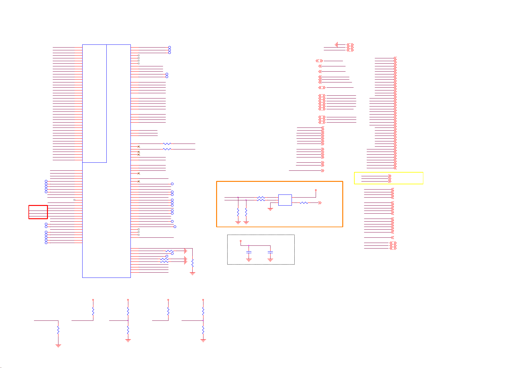
9-4-14 GPIO/servAD
CI_A0
CI_A1
CI_A2
CI_A3
CI_A4
CI_A5
CI_A6
CI_A7
CI_A8
CI_A9
CI_A10
CI_A11
CI_A12
CI_A13
CI_A14
CI_MCLKI
CI_MIVAL
CI_MISTRT
CI_MDI0
CI_MDI1
CI_MDI2
CI_MDI3
CI_MDI4
CI_MDI5
CI_MDI6
CI_MDI7
CI_D0
CI_D1
CI_D2
CI_D3
CI_D4
CI_D5
CI_D6
CI_D7
CI_MDO0
CI_MDO1
CI_MDO2
CI_MDO3
CI_MDO4
CI_MDO5
CI_MDO6
CI_MDO7
CI_RST
USB_OCP_P0
USB_EN_P0
USB_OCP_P1
USB_EN_P1
HUB_RESET
TP410
USB_OCP_P2
TP438
DE
TP412
VSYNC
TP414
HSY NC
TP415
LOCKn
I2SAMP_RESET
INV_EN
VIDEO_DET
TP422
TP437
TP439
TP444
TP445
TP446
TP421
PANEL_PWR_EN
CI_OCP
X_AUDIO_MON1
HP_MUTE
USB_EN_P2
CI_PWR _EN
SPK_MUTE
PWM1_DIMMER
PWM2_DIMMER
PWM3_DIMMER
PANEL_PWM_M
YPBPR_D ETECT1
HP_DET
SYSEPROMWP_6262
AJ30
AG29
AE29
AG31
AF30
AJ29
AH29
AB28
AB27
AA27
AA28
AA30
AA22
AA21
E15
D15
E16
F15
B10
E11
G15
H15
Y22
Y21
G1
G2
F3
E1
D1
D2
C2
K5
D5
E5
B3
B1
J6
D3
E4
K7
H5
D4
C4
F5
G4
G6
H6
J7
J5
K4
H4
H3
J2
A7
C7
C5
B5
B4
J4
J3
J1
B7
C6
A5
A4
A3
C1
J10
F6
J15
J9
U401-8
CI_A0
CI_A1
CI_A2
CI_A3
CI_A4
CI_A5
CI_A6
CI_A7
CI_A8
CI_A9
CI_A10
CI_A11
CI_A12
CI_A13
CI_A14
CI_MCLKI
CI_MIVAL
CI_MISTRT
CI_MDI0
CI_MDI1
CI_MDI2
CI_MDI3
CI_MDI4
CI_MDI5
CI_MDI6
CI_MDI7
CI_D0
CI_D1
CI_D2
CI_D3
CI_D4
CI_D5
CI_D6
CI_D7
CI_MDO0
CI_MDO1
CI_MDO2
CI_MDO3
CI_MDO4
CI_MDO5
CI_MDO6
CI_MDO7
CI_RST
GPIO42
GPIO43
GPIO44
GPIO45
GPIO46
GPIO48
GPIO49
GPIO50
GPIO51
GPIO52
GPIO53
GPIO54
GPIO55
GPIO56
GPIO57
GPIO58
GPIO59
GPIO60
GPIO61
GPIO62
GPIO63
GPIO64
GPIO65
GPIO66
GPIO67
GPIO68
GPIO69
GPIO70
MT5802VGEJ
GPIO0
GPIO1
GPIO2
GPIO3
GPIO4
GPIO5
GPIO6
GPIO7
GPIO8
GPIO9
GPIO10
GPIO11
GPIO12
GPIO13
GPIO14
GPIO15
GPIO16
GPIO17
GPIO18
GPIO19
GPIO20
GPIO21
GPIO22
GPIO23
GPIO24
GPIO25
GPIO26
GPIO27
GPIO28
GPIO29
GPIO30
GPIO31
GPIO32
GPIO33
GPIO34
GPIO35
GPIO36
GPIO37
GPIO38
GPIO39
GPIO40
GPIO41
GPIO47
DEMOD_RST
DEMOD_TSCLK
DEMOD_TSDATA0
DEMOD_TSDATA1
DEMOD_TSDATA2
DEMOD_TSDATA3
DEMOD_TSDATA4
DEMOD_TSDATA5
DEMOD_TSDATA6
DEMOD_TSDATA7
DEMOD_TSSYNC
DEMOD_TSVAL
CI_IN T
CI_TSCLK
CI_TSDATA0
CI_TSSYN C
CI_TSVAL
PVR_TSCLK
PVR_TSVAL
PVR_TSSYNC
PVR_TSDATA0
PVR_TSDATA1
SPI_CLK1
SPI_CLK
SPI_DATA
SPI_CLE
OPWM0
OPWM1
OPWM2
SD_D0
SD_D1
SD_D2
SD_D3
SD_CMD
SD_CLK
VCC3IO_SD
LED_PWM0
LED_PWM1
LED_PWM2
LED_PWM3
OPCTRL0
OPCTRL1
OPCTRL2
OPCTRL3
OPCTRL4
OPCTRL5
OPCTRL6
OPCTRL7
OPCTRL8
OPCTRL9
OPCTRL10
OPCTRL11
OPCTRL12
OPCTRL13
OPCTRL14
OPCTRL15
OPCTRL16
OPCTRL17
OPCTRL18
OPCTRL19
OPCTRL20
OPCTRL21
OPCTRL22
ADIN0_SR V
ADIN1_SR V
ADIN2_SR V
ADIN3_SR V
ADIN4_SR V
ADIN5_SR V
ADIN6_SR V
ADIN7_SR V
ADIN8_SR V
ADIN9_SR V
D11
F10
E10
F11
G12
F12
D12
G14
H14
J14
D10
C11
E2
B8
G3
F4
B2
F2
A2
L7
E3
G5
K3
A8
C3
D6
AA31
AF29
AA29
H9
C8
E8
F8
G9
D7
A10
L30
N28
W29
L29
J29
K27
J30
R28
R29
M32
J27
K30
G30
L31
Y32
N32
R27
T24
T25
U26
N27
G29
M25
M26
U28
R26
R25
H29
K31
H28
K28
J28
L32
F30
N31
P22
N21
DEMOD_RST
DEMOD_TSCLK
DEMOD_TSDATA0
LNB_EN
LNB_LINEDR OP
13/18V_SW
DEMOD_TSSYNC
DEMOD_TSVAL
CI_IN T
CI_TSCLK
CI_TSDATA0
CI_TSSYN C
CI_TSVAL
PVR_TSCLK
PVR_TSVAL
PVR_TSSYNC
PVR_TSDATA0
PVR_TSDATA1
SPI_CLK1
SPI_CLK
SPI_DATA
SPI_CLE
DIMMER0
A_DIM_ADJ
DIMMER2
SD_D0
R451
SD_D2
R452
SYS_EEPROM_WP
VCC3IO_SD
LED_PWM0
LED_PWM1
LED_PWM2
DEMOD_RST_STBY
LED_G
WIFI _RESET
FB_PWR_C TRL
EWS_PWR
WHITE_LED
POWER_KEY
STBY_LED
DC_MON
TUNER_WAKEU P
WoWLAN_I RQ
ETHER_PWR_EN
AC_OFF_I NFO
MHL_PWR_EN
AMP_PWRDN
WIFI _PWR_EN
WoWBLE_IR Q
USB_MHL_OC
BL_ERR
PANEL_12V_MON
ADIN3_SR V
TU_DET
R454 10K 1/16W 5%
TU_ID
R455 10K 1/16W 5%
KEY_PAD0
REG19.5V_MON
AMBI_TEMP
TUN_LNB
TP432
TP433
TP434
TP435
TP436
PHILIPS USE OPWM1
AMBIL_SPI_DO
AMBIL_SPI_CLK
33R 1/16W 5%
33R 1/16W 5%
TP401
TP408
TP402
TP403
TP404
TP405
TP406
TP407
TP440
TP447
R453 10K 1/16W 5%
TP409
TP442
R415
10K 1/16W 5%
DIMMER0
DIMMER2
R464
DVDD3V3
R461
R462
NC/0R 05 1/16W
NC/0R 05 1/16W
NC/10K 1/16W 5%
NC/10K 1/16W 5%
Close to Main Chip
VCC3IO_SD
C4200
100N 16V
1
2
C4201
1uF 10V
SYS_EEPROM_WP6
SYSEPROMWP_6262
U430
5
B
VCC
A
4
GND3Y
NC/74LVC 1G08GW
WIFI _RESET16
USB_MHL_OC12
PANEL_PWR_EN11
POWER_KEY16
KEY_PAD016,22
HP_DET21
WoWLAN_I RQ16
LED_PWM06,16
LED_PWM16
LED_PWM26,16
FB_PWR_CTR L5
MHL_PWR_EN12
VIDEO_DET9
YPBPR_D ETECT19
CI_OCP15
CI_PWR _EN
CI_RST
HTPDn
A_DIM_ADJ
INV_EN
AMP_PWRDN
WIFI _PWR_EN
USB_EN_P0
USB_EN_P1
USB_OCP_P0
USB_OCP_P1
LOCKn
I2SAMP_RESET
R463
NC/0R 05 1/16WR466
DVDD3V3
3V3SB
DVDD3V3
WIFI _RESET
USB_MHL_OC
PANEL_PWR_EN
POWER_KEY
KEY_PAD0
HP_DET
WoWLAN_I RQ
LED_PWM0
LED_PWM1
LED_PWM2
FB_PWR_CTRL
MHL_PWR_EN
SYS_EEPROM_WP
VIDEO_DET
YPBPR_D ETECT1
CI_OCP
CI_PWR _EN 15
CI_RST 15
HTPDn 11, 21
A_DIM_ADJ 5
INV_EN 5
AMP_PWRDN 10
WIF I_PWR_EN 16
USB_EN_P0 18
USB_EN_P1 18
USB_OCP_P0 18
USB_OCP_P1 18
LOCKn 11
I2SAMP_RESET 10
SYSEPROMWP_6262 6
BL_DIG_DI M 5
Sony
GND 4,5,6, 7,8,9,10,11,12,13 ,14,15,16,18,19,2 0,21,22
3V3SB 4,5,6, 9,12,16,18,22
DVDD3V3 5,6,7, 9,10,11,14,15,18, 19,21,22
CI_A0
CI_A1
CI_A2
CI_A3
CI_A4
CI_A5
CI_A6
CI_A7
CI_A8
CI_A9
CI_A10
CI_A11
CI_A12
CI_A13
CI_A14
CI_MCLKI
CI_MIVAL
CI_MISTRT
CI_MDI0
CI_MDI1
CI_MDI2
CI_MDI3
CI_MDI4
CI_MDI5
CI_MDI6
CI_MDI7
CI_D0
CI_D1
CI_D2
CI_D3
CI_D4
CI_D5
CI_D6
CI_D7
CI_MDO0
CI_MDO1
CI_MDO2
CI_MDO3
CI_MDO4
CI_MDO5
CI_MDO6
CI_MDO7
AMBIL_SPI_DO
AMBIL_SPI_CLK
AMBI_TEMP
SPI_CLK
SPI_CLK1
SPI_DATA
SPI_CLE
CI_IN T
CI_TSCLK
CI_TSVAL
CI_TSSYN C
CI_TSDATA0
PVR_TSSYNC
PVR_TSCLK
PVR_TSDATA0
PVR_TSDATA1
PVR_TSVAL
CI_RST
TUN_LNB
LNB_EN
LNB_LINEDR OP
13/18V_SW
CI_A0 15
CI_A1 15
CI_A2 15
CI_A3 15
CI_A4 15
CI_A5 15
CI_A6 15
CI_A7 15
CI_A8 15
CI_A9 15
CI_A10 15
CI_A11 15
CI_A12 15
CI_A13 15
CI_A14 15
CI_MCLKI 15
CI_MIVAL 15
CI_MISTRT 15
CI_MDI0 15
CI_MDI1 15
CI_MDI2 15
CI_MDI3 15
CI_MDI4 15
CI_MDI5 15
CI_MDI6 15
CI_MDI7 15
CI_D0 15
CI_D1 15
CI_D2 15
CI_D3 15
CI_D4 15
CI_D5 15
CI_D6 15
CI_D7 15
CI_MDO0 15
CI_MDO1 15
CI_MDO2 15
CI_MDO3 15
CI_MDO4 15
CI_MDO5 15
CI_MDO6 15
CI_MDO7 15
AMBIL_SPI_DO 22
AMBIL_SPI_CLK 22
AMBI_TEMP 22
SPI_CLK 15
SPI_CLK1 15
SPI_DATA 15
SPI_CLE 15
CI_I NT 15
CI_TSCLK 15
CI_TSVAL 15
CI_TSSYN C 15
CI_TSDATA0 15
PVR_TSSYNC 15
PVR_TSCLK 15
PVR_TSDATA0 15
PVR_TSDATA1 15
PVR_TSVAL 15
CI_RST 15
TUN_LNB 14
LNB_EN 14
LNB_LINEDR OP 14
13/18V_SW 14
DEMOD_RST_STBY
TUNER_WAKEU P
R456
10K 1/16W 5%
DVDD3V3
R457
10K 1/16W 5%
Main_18V_12V
REG19.5V_MON
R458
NC/82K OHM 5% 1/16W
R459
NC/10K 1/16W 5%
DVDD3V3
X_AUDIO_MON1
R460
10K 1/16W 5%
PANEL_12V_MON
Panel_12V
R467
NC/47K 1/16W 5%
R468
NC/10K 1/16W 5%

9-4-15 USB/ETHERNET PHY
ETHERNET PHY
AVDD3V3
U401-10
MT5802VGEJ
USB_DP_P216
USB_DM_P216
AVDD33_USB
AVDD33_ETH_STB
AVDD10_ETH_STB
P33
TXVP_0
P32
TXVN_0
R30
RXVP_1
R31
RXVN_1
V28
PHYLED 0
U27
PHYLED 1
L28
REXT
K23
F27
USB_DP_P0
USB_DM_P0
USB_DP_P1
USB_DM_P1
USB_DP_P2
USB_DM_P2
SSUSB_TXP
SSUSB_TXN
SSUSB_RXP
SSUSB_RXN
AVDD33_USB
AVDD33_SSUSB_STB
AVDD33_USB_STB
AVDD10_SSUSB_STB
AVDD1V0_STB
C4148
10UF 6. 3V 20%
AVDD10_SSUSB_STB
TXVP_0
TXVN_0
RXVP_1
RXVN_1
REXT
AVDD33_ETH_STB
AVDD10_ETH_STB
U401-9
B11
USB_DP_P0
A11
USB_DM_P0
B12
USB_DP_P1
A12
USB_DM_P1
T32
USB_DP_P2
T33
USB_DM_P2
V32
SSUSB_TXP
V33
SSUSB_TXN
U30
SSUSB_RXP
U31
SSUSB_RXN
L18
AVDD33_USB
M21
AVDD33_SSUSB_STB
L25
AVDD33_USB_STB
W32
AVDD10_SSUSB_STB
MT5802VGEJ
Near IC
C4184
100N 16V
R445
24K 1%
C4160
10uF 6.3V
All P ath
Ground ing(20m il)
All P ath
Ground ing(20m il)
TXVP_0
TXVN_0
RXVP_1
RXVN_1
Must be differential 100ohm
SEPARATE GROUND
USB PORT 1 SIDE
All Pa th
Groun ding(20m il)
+5V_USB
500mA
C111
1uF 10V
USB_EN_P0
t
1 2
TH403 NC /PTCR
+5V_USB
40mil
U106
G529A1TB1U
IN3OUT
2
GND
1
EN
R1047
4.7K1/16W
HI = > P OWER ON
LO = > PO WER OFF
USB_DP_P0
USB_DM_P0
USB_PORT0_5V
4
5
OUT
6
OC
C4601
100N 16V
R1029
C4603
100N 16V
EQUAL LENGTH and
DIFFERENTIAL
IMPEDANCE 90ohm
R1025 2R2 1/16W 5%
R1026 2R2 1/16W 5%
R1030
33K 1/10W 5%
0103 Update
DVDD3V3
R1046
10K 1/16W 5%
H=> NORM AL
L =>OCP
C4602
10N 50V
0R05 OHM
C4604
10N 50V
C1015
C1016
+
100UF 16V
10PF 50V
R1049
1K 1/16W 5%
RJ45
9
CN107
1
P1
2
P2
3
P3
4
P4
5
P5
6
P6
7
P7 NC
8
P8
RJ45 8P
10
USB_DP_P0_R
USB_DM_P0_R
C1017
10PF 50V
USB_OCP_P0 17
All P ath
Ground ing(20m il )
1 2
SSUSB_RXN
SSUSB_RXP
SSUSB_TXP
SSUSB_TXN
2
3
t
NC/PTCR
C1111 100N 16V
C1112 100N 16V
1uF 10V
USB_EN_P1
USB_DP_P1
+5V_USB
USB_DM_P1
900mA
TH402
HI = > POWER ON
LO = > POWER
OFF
C4605
12
100N 16V
4
3
2
1
ZD108
NC/ AZ5125-01H.R7G
65
1234
C4606
10N 50V
CN113
USB CON N
TH1
TH2
12
ZD107
NC/ AZ5125-01H.R7G
for SONY
USB PORT 2 (USB 3.0)
90OHM
L104
1
R1105 2R2 1/16W 5%
4
R1106 2R2 1/16W 5%
USB_PORT1_5V
C1110
C1109
C1108
100UF 16V
+5V_USB
NC/10uF 16V
R1115
R1118
R1116
R1117
U108 G524B3T11U
5
4
R1027
4.7K1/16W
10uF 16V
0R05 1/16W
0R05 1/16W
0R05 1/16W
0R05 1/16W
IN
EN(EN)
+
EQUAL LENGTH and
DIFFERENTIAL
IMPEDANCE 90ohm
All Pa th Grou ndin g(20mi l)
C1018
C1119
10PF 50V
BOTTOM USB
VOUT
OC
GND
2
H=> NORMA L
L =>OCP
C1120
10PF 50V
SSUSB_RXN_R
SSUSB_RXP_R
SSUSB_TXP_R
SSUSB_TXN_R
12
ZD4103
NC/ AZ5125-01H.R7G
1
USB_PORT1_5V
3
R107 10K 1/ 16W 5%
12
ZD1102
NC/AZ 5125-01H.R7G
12
ZD4105
12
ZD1101
NC/AZ 5125-01H.R7G
12
ZD4104
NC/ AZ5125-01H.R7G
R1028
1K 1/16W 5%
BOT TOM
1D+3
VCC
USB3.0
RXN5RXP6GND7TXN8TXP
12
ZD4106
NC/ AZ5125-01H.R7G
USB_OCP_P1 17
DVDD3V3
11
4D-2
GND
USB2.0
HAND110HAND2
9
CN112
USB CON N 9P
NC/ AZ5125-01H.R7G
3V3SB
R477
0R05 1/16W
AVDD1V0_STB
AVDD10_ETH_STB
Near IC
AVDD33_USB_STB
C4202
100N 16V
C4182
NC/1uF 10V
3V3SB
AVDD33_SSUSB_STB
AVDD33_ETH_STB
R469
0R05 1/16W
C4186
NC/ 100N 16V
C145
100N 16V
USB_PORT0_5V
USB_EN_P0
USB_EN_P1
+5V_USB
+5V_SW
3V3SB
AVDD3V3
AVDD1V0_STB
AVDD1V0_1
OPWRSB_PWR
DVDD3V3
USB_PORT0_5V 5
USB_EN_P0 17
USB_EN_P1 17
+5V_USB 12
+5V_SW 4,5,12, 13,15,21,22
3V3SB 4,5,6, 9,12,16,22
AVDD3V3 5,9, 11,12,21
AVDD1V0_STB 5, 6,12
AVDD1V0_1 5,11,12
OPWRSB_PWR 4,5,22
DVDD3V3 5,6,7, 9,10,11,14,15,17, 19,21,22
GND 4,5,6, 7,8,9,10,11,12, 13,14,15,16,17,19,20, 21,22
18(12)V TO 5V FOR USB/MHL POWER
C8082 47pF 50V
R8064
C8080
100NF 25V
0R05 1/10W
R8057
13.3K 1%
8
IN
7
SS
6
SGND
5
FB
Main_18V_12V
R8058
0R05
Vout = 0.6V (1+( R1/R2
))
Vout = 0.6V (1+( 100/13.3
))=5.11V
⊙
⊙
C8079
10UF 16V
C8083
100N 50V
R8061 0R 05 1/16W
R8059 100K 1%
U713
SY8234FC C
1
LX
C8081
2
BS
3
100N 50V
EN
4
NC
PGND
9
R8062
270K
Vout = 0. 6x(1+ 100/13)=5. 21V
R8060
2.2 OHM 1/ 10W
R8063
10K 1/16W 5%
C8086
10N 50V
L803
4.7uH
OPWRSB_PWR
3.3A
C8084
10UF 10V
C8085
10UF 10V
+5V_USB
1 3
ZD4107
NC/BZ X84-C5V1
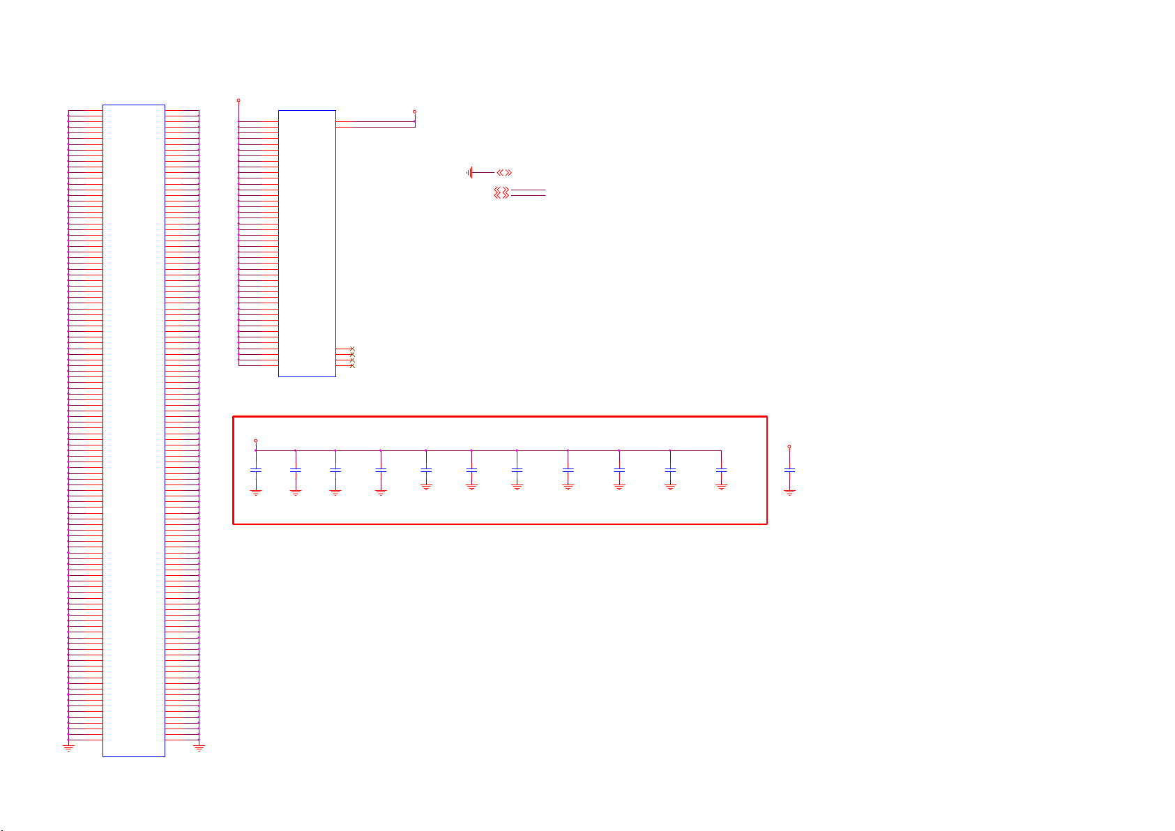
9-4-16 VCCK & DVSS
AF11
AM11
W12
W15
AF12
W16
W17
AA17
W13
AA13
AB13
AH10
W33
AC27
AC2
AF2
AE5
AA3
AD3
AG3
AH4
AG6
AH5
AE6
AB7
AB8
AC8
AF6
AE7
C10
H10
M11
N11
R11
AK8
M12
N12
R12
U12
Y12
R15
U15
AM8
R16
U16
R17
U17
Y17
M13
N13
R13
U13
N10
Y13
C13
C15
M14
C12
N14
U25
Y26
G27
Y2
P2
U2
AJ2
M3
R3
V3
P5
V5
B28
T6
M7
W6
AL4
E7
L6
D8
G8
T8
V8
R8
W8
AL5
T7
H8
AL7
P11
T11
P12
T12
V12
P13
P15
T15
V15
M8
E9
P16
T16
V16
P17
T17
V17
T13
V13
P10
P14
AJ4
T28
T29
U401-11
DVSS
DVSS
DVSS
DVSS
DVSS
DVSS
DVSS
DVSS
DVSS
DVSS
DVSS
DVSS
DVSS
DVSS
DVSS
DVSS
DVSS
DVSS
DVSS
DVSS
DVSS
DVSS
DVSS
DVSS
DVSS
DVSS
DVSS
DVSS
DVSS
DVSS
DVSS
DVSS
DVSS
DVSS
DVSS
DVSS
DVSS
DVSS
DVSS
DVSS
DVSS
DVSS
DVSS
DVSS
DVSS
DVSS
DVSS
DVSS
DVSS
DVSS
DVSS
DVSS
DVSS
DVSS
DVSS
DVSS
DVSS
DVSS
DVSS
DVSS
DVSS
DVSS
DVSS
DVSS
DVSS
DVSS
DVSS
DVSS
DVSS
DVSS
DVSS
DVSS
DVSS
DVSS
DVSS
DVSS
DVSS
DVSS
DVSS
DVSS
DVSS
DVSS
DVSS
DVSS
DVSS
DVSS
DVSS
DVSS
DVSS
DVSS
DVSS
DVSS
DVSS
DVSS
DVSS
DVSS
DVSS
DVSS
DVSS
DVSS
DVSS
DVSS
DVSS
DVSS
DVSS
DVSS
DVSS
DVSS
DVSS
DVSS
DVSS
DVSS
MT5802VGEJ
DVSS
DVSS
DVSS
DVSS
DVSS
DVSS
DVSS
DVSS
DVSS
DVSS
DVSS
DVSS
DVSS
DVSS
DVSS
DVSS
DVSS
DVSS
DVSS
DVSS
DVSS
DVSS
DVSS
DVSS
DVSS
DVSS
DVSS
DVSS
DVSS
DVSS
DVSS
DVSS
DVSS
DVSS
DVSS
DVSS
DVSS
DVSS
DVSS
DVSS
DVSS
DVSS
DVSS
DVSS
DVSS
DVSS
DVSS
DVSS
DVSS
DVSS
DVSS
DVSS
DVSS
DVSS
DVSS
DVSS
DVSS
DVSS
DVSS
DVSS
DVSS
DVSS
DVSS
DVSS
DVSS
DVSS
DVSS
DVSS
DVSS
DVSS
DVSS
DVSS
DVSS
DVSS
DVSS
DVSS
DVSS
DVSS
DVSS
DVSS
DVSS
DVSS
DVSS
DVSS
DVSS
DVSS
DVSS
DVSS
DVSS
DVSS
DVSS
DVSS
DVSS
DVSS
DVSS
DVSS
DVSS
DVSS
DVSS
DVSS
DVSS
DVSS
DVSS
DVSS
DVSS
DVSS
DVSS
DVSS
DVSS
DVSS
DVSS
DVSS
H16
J16
C24
D24
E24
F24
L16
AC16
F29
M17
C18
T30
A32
C20
C22
D22
H25
AJ25
G26
H26
E25
AL10
AJ26
AJ12
AL13
AM14
P21
AJ28
AE31
T31
W22
V22
U22
V31
F9
AG20
AC31
N20
AL19
AH32
N33
W21
V21
U21
T21
R21
AF19
N19
AA20
Y20
W20
V20
U20
T20
R20
P20
P18
N18
N17
C17
AA19
Y19
W19
V19
U19
T19
R19
P19
AF16
AE16
AA16
Y16
N16
AA18
Y18
W18
V18
U18
T18
R18
M16
AF15
AB15
AA15
Y15
N15
M15
AL16
AB14
AA14
Y14
W14
V14
U14
T14
R14
AL22
R10
K15
AC13
AC12
AM20
AM17
T22
L5
F20
V29
K6
F7
J8
G10
AD27
VCCK
AC19
AD21
AC20
AD20
AC21
AC17
AC22
AC18
W23
AA23
AB23
AC23
AD23
W24
AA24
AB24
AC24
AD24
AB25
AC25
AD25
AE25
AF25
AD26
AE26
AF26
AG26
AF24
AA25
AG25
AF27
AG27
AE21
AE24
W25
AH26
AB17
AB18
Y23
Y24
V23
V24
V25
Y25
U401-12
VCCK
VCCK
VCCK
VCCK
VCCK
VCCK
VCCK
VCCK
VCCK
VCCK
VCCK
VCCK
VCCK
VCCK
VCCK
VCCK
VCCK
VCCK
VCCK
VCCK
VCCK
VCCK
VCCK
VCCK
VCCK
VCCK
VCCK
VCCK
VCCK
VCCK
VCCK
VCCK
VCCK
VCCK
VCCK
VCCK
VCCK
VCCK
VCCK
VCCK
VCCK
VCCK
VCCK
VCCK
MT5802VGEJ
Capacitor s close to IC
VCCK
C4141
C4175
22UF
22UF
VCC3IO_A
VCC3IO_B
NC
NC
NC
NC
L2
AH33
AN33
A33
AN1
A1
C4166
NC/10uF 6.3V
VCC3IO_A
VCC3IO_B
VCC3IO_AB
C4152
4.7UF 6.3V
C4158
NC/100N 16V
VCCK4,5,6,7
DVDD3V35,6,7,9, 10,11,14,15,17,18, 21,22
C4161
NC/100N 16V
GND 4,5,6, 7,8,9,10,11,12,13, 14,15,16,17,18,2 0,21,22
VCCK
VCC3IO_AB
C4162
NC/100N 16V
C4144
100N 16V
C4145
1uF 10V
C4165
NC/100N 16V
C4147
100N 16V
VCCK
C4193
1uF 10V

9-4-17 DDP POWER
R475
47R 1/ 16W 5%
DDR VREF_C 1
CRTN
ZQ_C1
DDR V
R440
240R 1%
U401-13
K2
DDR VREF_C 1
L9
CRTN
L4
ZQ_C1
N9
DDR V
AG8
AA9
AF9
T10
U10
Y9
P9
DDR V
DDR V
DDR V
DDR V
DDR V
DDR V
DDR V_CKC
MT5802VGEJ
DDR V
DDR V
DDR V
DDR V
DDR V
DDR V
DDR V
DRAM Power
V10
W10
Y10
AA10
AB10
AC10
AC11
DDR V
DDR V
R441
1K 1/16W 1%
DDR VREF_C 1
R442
1K 1/16W 1%
C4128
100N 16V
C4127
100N 16V
DDR V
C4099
100N 16V
C4085
1uF 10V
DDR V5,7,8
C4130
100N 16V
DDR V
GND 4,5,6,7,8,9,10, 11,12,13, 14,15,16,17,18,19, 21,22
DDR V
Cap close to DDRV power source.
C4173
1UF 6.3V
C4115
100N 16V
C4132
100N 16V
C4133
100N 16V
C4094
100N 16V
C4093
100N 16V
C4136
100N 16V
C4092
100N 16V
Bottom Side Capacitors close to IC
DDR V
C4124
10uF 6. 3V
C4135
100N 16V
C4072
100N 16V
C4134
100N 16V
C4131
100N 16V
+
C4139
NC/ 47uF 16V
C4168
1uF 10V
C4167
10uF 6.3 V
C4169
100N 16V
C4098
4.7UF 6.3V
C4170
100N 16V
C4095
10uF 6. 3V
C4171
100N 16V
C4172
100N 16V

9-4-18 LINE OUT
AIN_R 0
AIN_L0
TP103
TP104
AVDD33_AADC
VMID_AADC
C4153
100N 16V
HEADPHONE
AR0O
All Pa th
Grounding(20mil)
U401-4
D26
AIN_R 0
A26
AIN_L0
C26
AIN_R 1
B27
AIN_L1
C4154
1UF 6.3V
B26
AIN_R 2
C27
AIN_L2
K21
AVDD33_AADC
D29
VMID_AADC
K22
AVSS33_CLN
MT5802VGEJ
C682
+
100UF 16V
for PCB
space
C683
+
100UF 16V
AIN_R 2 AR1O
AIN_L2
AVSS33_CLN
AVDD33_ADAC
OUTR
OUTL
R675
R676
22K 1/16W 5%
AL0_ADAC
AR0_ADAC
AL1_ADAC
AR1_ADAC
ASPDIF O0
ASPDIF O1
AOSDATA4
AOSDATA3
AOSDATA2
AOSDATA1
AOSDATA0
22K 1/16W 5%
ASPDIFI
AOBCK
AOLRCK
AOMCLK
10R 1/ 10W 5%
10R 1/ 10W 5%
A28
AL0O
C28
AR0O
C29
AL1O
D28
J21
AVDD33_ADAC
AG30
HTPDn
Y33
ASPDIFO0
F17
ASPDIFO1
AK32
AOBCK
AJ31
AOLRCK
AL33
R101 22R 1/ 16W 5%
AH30
AJ33
AJ32
AH31
AOSDATA1
AK33
AOSDATA0
R653
R654
HPOUTR
C660
NC/ 6.8NF 50V
HPOUTLAL0O
C661
NC/ 6.8NF 50V
HP Audio o ut
AL1O 22
AR1O 22
HTPDn 11
TP101
wi th GND
R655 0R05 1/16W
AOMCLK
C4204
10PF 50V
HP_DET
Low: normal
High: HP detect
HP_DET
HPOUTR
HPOUTL
with GND
AVDD3V3
R646
R647
0R05 1/10W
0R05 1/10W
AVDD33_AD AC
ARC
C1033
33P 50V
C653
100N 16V
Analog Power
AVDD33_AADC
C4150
NC/ 100N 16V
33R 1/ 16W 5%
R619
NC/ 0R05 1/16W
C654
100N 16V
SPDIF _OUT
12
ZD131
NC/ TVM1G5R 5M100R
12
ZD132
R656
C4157
10uF 6. 3V
C1043
10PF 50V
DVDD 3V3
R641
NC/ 4K7 1/16W 5%
C662
NC/ TVM1G5R 5M100R
NC/ 470pF 50V
Spdif Out
with GND
R1138
0R05 1/16W
R618 0R05 1/16W
3
4
2
5
1
12
CN602
PHONE JACK 5P
ZD129
NC/ TVM1G5R 5M100R
+5V_SW
C1026
100N 16V
ARC
AOMCLK
AOBCK
AOLRCK
AOSDATA0
HP_DET
AIN_R 0
AIN_L0
+5V_SW
AVDD3V3
DVDD 3V3
CN104
OPTICAL
1
VIN
2
VCC
3
GND
TH14TH25TH36TH4
7
ARC 12
AOMCLK 10
AOBCK 10
AOLRCK 10
AOSDATA0 10
HP_DET 17
AIN_R 0 9
AIN_L0 9
GND 4,5, 6,7,8, 9,10,11,12,13,14,15,16,17,18,19,20,22
+5V_SW 4,5,12,13,15,22
AVDD3V3 5, 9,11,12, 18
DVDD 3V3 5,6,7,9,10, 11,14,15, 17,18,19, 22
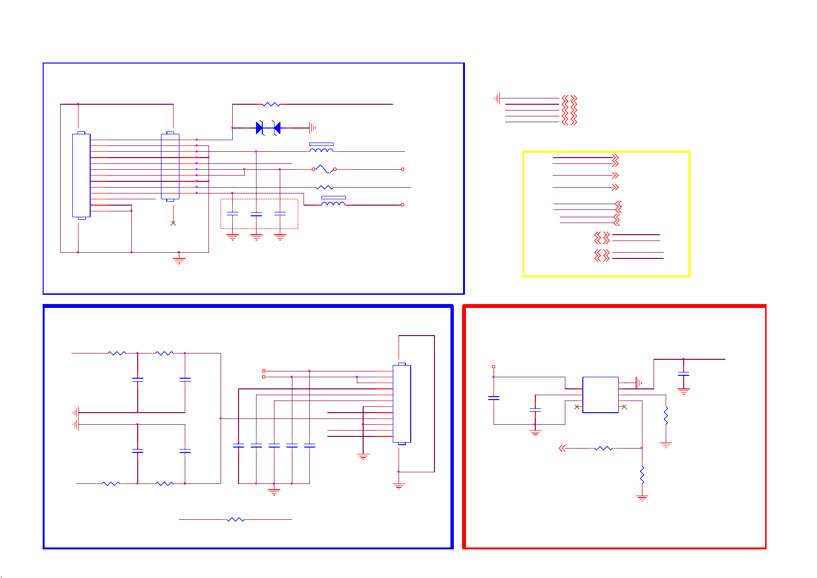
9-4-19 AMBILIGHT & Hotel TV
AL+KEY
R4501
C403
NC/ 1nF 50V
+5V_SW
C415
R4503
0R05 1/ 16W
ZD127
1 2
3V3SB
NC/ 100P 50V
1415
CN416
NC/ COMM
1
2
3
4
5
6
7
8
9
10
11
12
13
AMBI_PWR
1112
CN412
CONN
1
2
3
4
5
6
7
8
9
10
Key 1
AMBIL_SPI_DO
AMBI_PWR
AMBI_3V3
2W Mono Speaker output for BUH Hotel TV
Close to SoC
AL1O
NC/ 200R 1/ 16W 5%
AR1O
NC/ 200R 1/ 16W 5%
R4504
R4506
R4505
NC/ 510R 1/ 16W 5%
C4501
NC/ 1nF 50V
C4503
NC/ 1nF 50V
R4507
NC/ 510R 1/ 16W 5%
C4502
NC/ 10NF 50V
C4504
NC/ 10NF 50V
PWRD N
100R 1/ 16W 1%
AZ5123-01H
C402
C404
100P 50V
100N 50V
C416
C417
NC/ 100P 50V
NC/ 100P 50V
For shutdown 12V
SPK_SD
1 2
FB716 120R 3A
F1401 NC/T 2A 63V
R4502 0R05 1/16W
1 2
FB715 N C/120R 3A
M od ify by EMI
1210 pin updated
OPWRSB_PWR
IR_SSB
IR_R C
SPK_SD
U0TX
C419
NC/ 100P 50V
U0RX
C418
NC/ 100P 50V
KEY_PAD0
AMBIL_SPI_CLK
AMBI_TEMP
12
11
10
9
8
7
6
5
4
3
2
1
18V_12V
DVDD 3V3
13 14
CN413
NC/ CONN
18V_12V
3V3SB
+5V_SW
DVDD 3V3
8/20 Add for PHP
AMBIL_SPI_DO
AMBIL_SPI_CLK
AMBI_TEMP
KEY_PAD 0
OPWRSB_PWR
PWRD N
AL1O
AR1O
IR_SSB6,16
IR_R C16
U0TX6
U0RX6
AL POWER CONTROL
18V_12V
1
2
C460
1UF 10% 16V
OPWRSB_PWR4,5,18
C461
22N 50V
3
GND 4,5,6,7,8,9,10, 11,12,13, 14,15,16, 17,18,19,20,21
18V_12V 4,5,11,14
3V3SB 4,5,6,9, 12,16,18
+5V_SW 4,5, 12,13,15, 21
DVDD 3V3 5,6,7,9,10,11,14, 15,17,18, 19,21
AMBIL_SPI_DO 17
AMBIL_SPI_CLK 17
AMBI_TEMP 17
KEY_PAD0 16,17
OPWRSB_PWR 4,5,18
PWRD N 10
AL1O 21
AR1O 21
IR_SSB
IR_R C
U0TX
U0RX
AMBI_PWR
U712
APL3546A KAI-TRG
VIN
SS
GND
NC4NC
R479 0R05 1/16W
GND
VOUT
ISET
9
8
7
6
EN
5
R480
NC/ 10K 1/16W 5%
C464
10uF 25V
R481
270K
270K ---> 1.8A
220K ---> 2.3A

9.5 B 715G8885 SSB (For 55/65” OLED873 series)
9-5-1 GPIO List
GPIO LIST
PIN NAME
CI_A0
CI_A1
CI_A2
CI_A3
CI_A4
CI_A5
CI_A6
CI_A7
CI_A8
CI_A9
CI_A10
CI_A11
CI_A12
CI_A13
CI_A14
CI_MCLKI
CI_MIVAL
CI_MISTRT
CI_MDI0
CI_MDI1
CI_MDI2
CI_MDI3
CI_MDI4
CI_MDI5
CI_MDI6
CI_MDI7
CI_D0
CI_D1
CI_D2
CI_D3
CI_D4
CI_D5
CI_D6
CI_D7
CI_MDO0
CI_MDO1
CI_MDO2
CI_MDO4
CI_MDO5
CI_MDO6
CI_MDO7
GPIO_42
GPIO_43
GPIO_44
GPIO_45
GPIO_46
GPIO_47
GPIO_48
GPIO_49
GPIO_50
GPIO_51
GPIO_52
GPIO_53
GPIO_54
GPIO_55
GPIO_56 JTAG JTD O
GPIO_57 JTCK
GPIO_58 JTMS
GPIO_59
GPIO_60
GPIO_61
GPIO_62
GPIO_63 SDIO POWER CONTROL SDIO_PWR_C TRL
GPIO_64
GPIO_65
GPIO_66
Function Definition
CI Interface
CI Interface
CI Interface
CI Interface
CI Interface
CI Interface
CI Interface
CI Interface
CI Interface
CI Interface
CI Interface
CI Interface
CI Interface
CI Interface
CI Interface
CI Interface
CI Interface
CI Interface
CI Interface
CI Interface
CI Interface
CI Interface
CI Interface
CI Interface
CI Interface
CI Interface
CI Interface
CI Interface
CI Interface
CI Interface
CI Interface
CI Interface
CI Interface
CI Interface
CI Interface
CI Interface
CI Interface
CI Interface
CI Interface
CI Interface
CI Interface
CI Interface
CI Over Current Protect
USB Power Enable
SYSTEM EEPROM write protect
CI Interface
CI POWER CONTROL
VB1 VB1_REQ
VB1
JTAG
JTAG
JTAG
JTAG
GPIO Function
CI_A0
CI_A1
CI_A2
CI_A3
CI_A4
CI_A5
CI_A6
CI_A7
CI_A8
CI_A9
CI_A10
CI_A11
CI_A12
CI_A13
CI_A14
CI_MCLKI
CI_MIVAL
CI_MISTRT
CI_MDI0
CI_MDI1
CI_MDI2
CI_MDI3
CI_MDI4
CI_MDI5
CI_MDI6
CI_MDI7
CI_D0
CI_D1
CI_D2
CI_D3
CI_D4
CI_D5
CI_D6
CI_D7
CI_MDO0
CI_MDO1
CI_MDO2
CI_MDO3
CI_MDO4
CI_MDO5
CI_MDO6
CI_MDO7
CI_OCP
USB_PWR _EN1
USB_PWR _EN2USB Power Enable
SYS_EEPROM_WP
CI_RESET
CI_POWER_EN
VB1_HTP DN_OSDVB1
VB1_LOCKN_OSD
JTDI
JTRST#
USB_PWR _EN0USB Power Enable
(GPIO_0)
(GPIO_1)
(GPIO_2)
(GPIO_3)
(GPIO_4)
(GPIO_5)
(GPIO_6)
(GPIO_7)
(GPIO_8)
(GPIO_9)
(GPIO_10)
(GPIO_11)
(GPIO_12)
(GPIO_13)
(GPIO_14)
(GPIO_15)
(GPIO_16)
(GPIO_17)
(GPIO_18)
(GPIO_19)
(GPIO_20)
(GPIO_21)
(GPIO_22)
(GPIO_23)
(GPIO_24)
(GPIO_25)
(GPIO_26)
(GPIO_27)
(GPIO_28)
(GPIO_29)
(GPIO_30)
(GPIO_31)
(GPIO_32)
(GPIO_33)
(GPIO_34)
(GPIO_35)
(GPIO_36)
(GPIO_37)
(GPIO_38)
(GPIO_39)
(GPIO_40)
(GPIO_41)
PIN NAME GPIO Function
ADIN0_ SRV
ADIN1_ SRV
ADIN2_ SRV
ADIN3_ SRV
ADIN4_ SRV
ADIN5_ SRV
ADIN6_ SRV
ADIN7_ SRV
ADIN8_ SRV
ADIN9_ SRV
PIN NAME GPIO Function
OPWM0
OPWM1
OPWM2
OPWM3
OPWM4
OPWM5
OPWM6
OPWM7
OPWM8
PIN NAME GPIO Function
LED_PW M0
LED_PW M1
LED_PW M2
LED_PW M3
PIN NAME
OPCTRL 0
OPCTRL 1
OPCTRL 2
OPCTRL 3
OPCTRL 4
OPCTRL 5
OPCTRL 6
OPCTRL 7
OPCTRL 8
OPCTRL 9
OPCTRL 10
OPCTRL 11
PCBA version ID
Function define
Function Select
KEY_PAD
KEY_PAD
MHL Over Current Protect
USB over current detect
USB over current detect
Demod
SD Card Detect SD_DET
Function define
Backlight DIMMING
LNA_AGC switch
Function define
Strapping / Standby mode LED
Strapping / Power On LED
Strapping Strap[1]
Function define
PHY LED
PHY LED
SCART
Backlight Control
PWM AMP MUTE
Headphone Detect
MHL_PWR_ENCI_MDO3
LVDS Power Control
USB Power Enable
Audio Mute Control
PCBA version ID
SCART_FS
KEY_PAD0
KEY_PAD1
USB_MHL_OC
USB_OC_P0/P1
USB_OC_P2/P3
RF AGCI
BL_DIMMING
LNASW_AGCSW
/ LED_PWM0
Strap[3]
/ LED_PWM1
Strap[2]
GPIO Function
PHYLED2
PHYLED3
AV_LINK
FB_PWR_CT RLFast Boot Control
BL_ON/OFF
AMP_MUTE
HP_DET
MHL_PWR_EN
LVDS_PWR_ EN
USB_PWR_E N3
MUTE_CTL

9-5-2 Power 1
2K17 MT5802 platform
CN701
16
15
14
NT-LCD-PWR -ON
AU_12V
Main_18V_12V
MAIN POWER
+12V
Big p la ne
R798
100K 1/16W 5%
C778
C779
10UF 16V
10UF 16V
C777
100NF 25V C 780
Vout = 0.6V (1+( R1/R2
))
Vout = 0.6V (1+( 100/(10+3.3)
))=5.19V
For 12V Only
+5V_STB
R744
15K 1/16W
⊙
⊙
ANALOG POWER AVDD1V05_STB
R779
0R05
R762
3K3 1/16W 5%
12
10
8
6
4
2
8
7
1
5
4.7UF 6.3V
9
C797
2.2UF 10V
13
11
9
7
5
3
1
CONN
U708
IN
IN
EN
VC
GND
SY8366QNC
6A(Spec.)
C798
100N 16V
R761
NC/100K1/1 6W
C792
NC/100N 16V
STB_PWR
2
PG
C781
6
BS
100N 50V
10
LX
4
FB
3
ILMT
U710 G5725ADJ T11U
4
VIN
1
EN
VFB
GND
2
BL_ON/POK
BL_DIG_DI M
ACD
OPWRSB_PWR
NC/BZ T52-B22
NC/BZ T52-B22
ZD707
ZD708
C707 100N 16V
C708 100N 16V
C709 100N 16V
Mo dify by EM I
Big p la ne
R796
10K 1%
3
LX
5
MAX=2.3A
Main_18V_12V
12
12
AU_12V
Main_18V_12V
2017/6/22 released(All NC)
R745
2.2R 1%
L702
3.3UH
R794
C785
100K 1/10W 1 %
R1
R795
R2
3K3 1%
L710 2. 2uH
R775
NC/100OHM
C793
NC/10N F 50V
R773
2Kohm 1/16W +/-1%
Vout=0.6 x (1+20000/26000)= 1.06 V
3N9 50V
R703
TYP = 300mA
C794
R702
NC/22P 50V
20K 1%
R704
24K 1%
1K 1/10W 1%
Big p la ne
C766
R786
NC/ 10K 1/16W 5%
Vout = 0.6V (1+( 100/(5.1+0.16)
))=12V
MAX=3A
Big p la ne
C787
22UF 10V
ZD704
RLZ6V2B
1 2
AVDD1V0_STB
R707
0R05
C790
NC/10U F 10V
ZD705
1 2
C799
10UF
MMSZ4678
NC/ 10UF 25V
C767
NC/ 10UF 25V
C768
R787
NC/100N 16V
NC/100K 1/16W 5%
C769
NC/4. 7UF 6.3V
⊙
R782
C702
100UF 16V
⊙
+5V_STB
0R05
C724
2.2UF 10V
Vout = 0.6V (1+( R1/R2
))
+
R7001 0R05 7A 1/4W
U701
8
IN
7
IN
1
EN
5
VC
9
GND
NC/SY 8366QNC
ILMT
PG
BS
LX
FB
2
C770
6
NC/ 100N 50V
10
4
3
R7047
NC/2. 2R 1%
Big p la ne
6A(Spec.)
R791
NC/160R 1/16W
INVERTER_ON_ OFF
BL_ON/OFF:
Inverter o n:High
Inverter o ff: Low
ACD
ACD :
High : Don 't care
Low : Shut down BL-O N(24V)
R2
R790
R4404
10K 1/16W 5%
10K 5% 1/16W
L705
NC/3.3UH
R789
R1
NC/5. 1K 1%
R768
NC/4. 7K1/16W
+3V3
R4407
+5V_STB
NC100K 1/ 10W 1%
R765
820R 1% 1/ 16W
NC/4. 7K1/16W
R763
4.3K 1%
23
BTA1576S31
Q4309
NC/ 470PF
R792
NC/ 1K 1/10W 1%
16V to 12V for Panel Vcc
For PSU 16V only
DVDD3V33V3SB
R769
NC/ 4.7K1/16W
Q711
NC/ MMBT3904
R770
R4405
10K 5% 1/16W
R4406
10K 5% 1/16W
C4411
NC/10000pF 50V
U707
SY8089AAAC
4
LX
IN
GND
5
EN
FB
2A
R2
R742
18K OHM 1% 1/ 16W
Big p la ne
MAX=3A
C774
C771
10UF 25V
R771
0R05 OHM
C796
NC/10uF 6.3V
Add on 2018/1/18
ZD4304
12
MM3Z3V6B
Q4308
LBC847BWT1G
3
L704
2
1
R748
4.7K 1/16W
+12V
C775
BL_ON/POK
R4408
0R05 1/16W
2.95A
2.2uH
+5V_STB
VCC&GND
+5V_STB
VCCK
DVDD 3V3
3V3SB
AVDD1V0_1
AVDD1V0_STB
AU_12V
OPWRSB
OPWRSB_PWR
10UF 25V
BL_ON/POK
INVERTER_ON_ OFF
BL-I-CTR
NT-LCD-PWR -ON
OPWRSB_PWR
BL_DIG_DI M
NC/100R
+5V_STB
DVDD3V3
3V3SB
AVDD1V0_1
AVDD1V0_STB
AU_12V
3V3SB
C704
NC/10uF 6.3V
MMBT3904
DVDD3V3 DVD D3V3
R712
Q703
NC/MMBT3904
5,9,12,14,1 6
5,6,7,17
VCCK
5,6,7,9, 10,11,14,15,16,17, 19
5,6,9,12, 14,16,20
11,12
6,12,16
10
OPWRSB
OPWRSB_PWR
INVERTER_ON_ OFF15,24,26
BL-I-CTR
NT-LCD-PWR -ON
R709
10K 1%
Q710
R706
NC/10K 1/16W 5%
R711
NC/0R 05 1/16W
R714
NC/4. 7K1/16W
6
5,20
15,24
11,24
OPWRSB:
Normal: Low
Stand_by: Hi
R767
OPWRSB
4.7K1/16W
R705
NC/4. 7K1/16W
BL-I-CTR
Normal :Max:+3V3 , Min:0 V
Stand _By:0V
R715
47K 1/16W 5%
BL-I-CTR
All NC 01/18
R750
3V3SB
R1
R746
75K 1/16W 1%
C711
33PF 50V
R751
6K2 1/10W 1%
1 2
ZD706
BZT52-B3V6
C725
10UF 10V
0 OHM 1/8W
C729
10UF 10V
R713 0R05
AVDD1V0_1AVDD1V0_STB

9-5-3 PSU CNN & Power 2
R784
0R05
⊙
⊙
R772
R760
100R 1/16W 5%
0R05
Big p lan e
C745
10UF 16V
10UF 16V
C747
3V3SB
C722
100N 16V
DDR_PW R_EN
+12V
OPWRSB_PWR
SY8368QNC: Max:8A
Vin 4V~25V
Vout = 0.6V (1+( R1/R2
))
Vout = 0.6V (1+( 24/36
))=1.0V
For 12V Only
+5V_STB
DDR_PWR_EN
FB enable(power on):high
FB disable(power off):low
U706
8
C746
IN
7
IN
1
EN
5
100NF 25V
LDO
4.7UF 6.3V
9
GND
SY8368QNC
R747
10K 1/10W 5 %
R729
100R
C723
C765
10UF 10V
10UF 10V
3.0A(Spec.)
C740
2
PG
6
BS
10
LX
4
FB
3
ILMT
36K 1%
U705
RT8079ZQW
1
VIN
2
VIN
3
GND
4
GND
R754
1.5nF 50V
R755 180K 1%
C749
100N 50V
Big p lan e
R710
16
17
GND
AGND5FB6COMP7RT/SYN C
20K
PGOOD
VIN
R743
2.2R 1%
C719 100N 16V
13
14EN15
BOOT
PGOOD
SW
SW
SW
SS/TR
8
R708
24K 1%
PGOOD
Normal:open drain by pull-up vlotage timing
TP448
Abnormal:low
L703
R725
1K
R1R2
0.68uH
R700
C750
3N9 50VC748
1R 1%
Big pla ne
ZD712
MMSZ4678
R741
1 2
10 OHM 1%
R737 1R 1%
Vout=0.827 x (1+27K/33K) = 1.5V)
12
11
L701
10
1.5uH
9
C726 10N 50V
R1
R2
R749
24K 1%
ZD701
1 2
R753
3K 1%
R701
33K 1/16W 1%
C758
C757
22uF 6.3V
22uF 6.3V
DRAM Power
C733
NC/BZ T52H-C2V7
22UF
C734
22UF
C759
22uF 6.3V
R736
0R05
R732
0R05
R731
0R05
R730
0R05
C760
22uF 6.3V
DDRV
MAX=1.6A
VCCK
18(12)V TO 5V FOR USB/MHL POWER
+12V
R8058
0R05
Vout = 0.6V (1+( R1/R2
))
Vout = 0.6V (1+( 100/13.3
))=5.1V
⊙
⊙
C8079
10UF 16V
C8083
100N 50V
C8080
100NF 25V
C8082 47pF 50V
R8059 100K 1%
R8064
1K 1/10W 1%
8
7
6
5
R8057
13.3K 1%
IN
SS
SGND
FB
U713
SY8234FCC
PGND
9
BS
EN
NC
R8061
LX
VCC&GND
AU_12V
VCCK
AVDD1V2
AVDD3V3
DVDD3V3
3V3SB
+5V_SW
AVDD1V0_1
AVDD1V0_STB
+5V_STB
GPIO
DDR_PW R_EN
OPWRSB_PWR
0R05 1/16W
1
C8081
2
3
4
100N 50V
R8062
AU_12V
VCCK
AVDD1V2
AVDD3V3
DVDD3V3
3V3SB
+5V_SW
AVDD1V0_1
AVDD1V0_STB
+5V_STB
DDR_PW R_EN
OPWRSB_PWR
Vou t = 0. 6x(1+ 100/13)= 5.21V
R8060
2.2 OHM 1/ 10W
R8063
10K 1/16W 5%
100K 1/16W 5%
C8086
10N 50V
3.3A
L803
4.7uH
OPWRSB_PWR
4,10
6,7,17
9
9,11,12,16, 19
4,6,7,9, 10,11,14,15,16,17, 19
4,6,9,12, 14,16,20
12,13,19,20, 24,29
4,11,12
4,6,12,16
4,9,12,14, 16
15
4,20
+5V_USB
C8085
C8084
10UF 16V
10UF 16V
DVDD3V3
C752
2.2UF 10V
R723
3K3 1/16W 5%
+5V_SW
C706
10uF 16V
R752
3K3 1/16W 5 %
C743
100N 16V
C727
100N 16V
C738
U709
G5725ADJT11U
4
1
C730
NC/100N 16V
R739
100K 1/16W 5%
NC/100N 16V
3
VIN
LX
5
EN
VFB
GND
2
Vout=0.6 x (1+100000/22000)= 3.32 V
U702 G5719TBIU
4
VIN
1
EN
GND2NC
C714
NC/10N F 50V
3
LX
6
VFB
C739
NC/10N F 50V
5
L711 2. 2uH
R727
NC/100OH M
R776
24K 1%
L707 2. 2uH
R759
NC/100OH M
R757
1K5 1%
Max : 800 mA
C717
NC/22P 50V
24K 1%
R734
0R05 OHM
ZD711
1 2
AVDD1V2
C751
10UF 6. 3V 20%
MMSZ4678
Vout=0.6 x (1+24000/24000)= 1.2V
R758
C728
NC/22P 50V
R756
20K 1%
100K 1%
C721
NC/10U F 10V
C705
10UF 16V
1 2
Sony req ues t
ZD703
BZT52-B3V6
C744
10UF 6. 3V 20%
(1A/60mil)
R716
0 OHM 1/8W
R717
0 OHM 1/8W
R8160
0 OHM 1/8W
DIGITAL POWER
DVDD3V3/AVDD3V3
DVDD3V3
C712
10UF
R724 10KOHM
+5V_SW
C731
100N 16V
DVDD3V3
AVDD3V3
+3V3
R764
10KOHM
U704
E-Pad
1
POK
GND
2
VEN
3
VIN
VPP4NC
C718
1uF 10V
2.0A(Spec.)
R735
1.65K 1%
G9661-25ADJF11U
9
8
7
ADJ
6
VO
5
R1
R2
eMMC 1V8
(1A/60mil)
ZD710
R728
2K 1%
1 2
R766
100R 1/16W 1%
LDO_PWR
R726
0R05
C715
BZT52H-C 2V7
10UF
0.8 x (1+ 2.1K/1.65K) = 1.8V
+5V_STB TO +5V_SW BY VCCK
If PSU has 3V3SB, all
conponents are
existing.
If PSU has 3V3SB, all
conponents are NC.
VCCK
R740
820 OHM 5% 1/ 16W
C701
100N 16V
+5V_STB
R781
8
7
6
5
C716
1UF16V
R733
33K 1/10W 5%
R738
22KOHM 1/10W
Q707
MMBT3904
+5V_SW
NC/0R 05R777
Q706
1
D
D
2
D
D
3
D
D
G4S
AON4421
+5V_S TB TO +5V_SW BY V CCK
MAX=2.0A
C786
22UF 10V

9-5-4 Peripheral
close to SOC
U401-7
R4030
4.7K1/16W
EMMC_RST#EMMC_RSTB
C4033
100N 16V
AM33
AL32
W30
W31
B30
A30
L24
AG33
K25
L21
L23
F28
K33
POWE#1
VCC3IO_EMMC
OSDA0
OSCL0
OSDA1
OSCL1
XTALI
XTALO
AVDD33_PDW _STB
VCC3IO_EMMC
AVDD33_RGB_STB
AVSS33_RGB
AVDD33_PLL_STB
AVDD10_PDW _STB
POR_OPT
MT5802UHOJ
C4035
1uF 10V
VCC_EMMC
TP4430
TP4431
TP4432
POCE1__B
POCE0__B
EMMC_CLK
EMMC_RSTB
EMMC_DS
FSRC_W R
R4041 NC/10K 1/ 16W 5%
R4034 NC/10K 1/ 16W 5%
R4038 NC/10K 1/ 16W 5%
R4037 NC/10K 1/ 16W 5%
R4039 NC/10K 1/ 16W 5%
R4033 NC/10K 1/ 16W 5%
R4036 NC/10K 1/ 16W 5%
R4035 NC/10K 1/ 16W 5%
R4040 NC/10K 1/ 16W 5%
A3
A4
A5
A6
A7
B2
B3
B4
B5
B6
C2
C4
C5
C6
D4
E5
E6
E7
E8
E9
E10
F5
F10
G3
OSDA0
OSCL0
OSDA1
OSCL1
XTALI
XTALO
AVDD33_PDW_ STB
Close t o main chip
EMMC_CLK EMMC_CLK#
VCC3IO_EMMC
C414
AVDD33_RGB_STB
1uF 10V
AVSS33_RGB
AVDD33_PLL_STB
AVDD10_PDW_ STB
POR_OPT
R5030 0R05 1/16W
EMMC
POWE__B
R5036 0R05 1/16W
PAALE
R5139 0R05 1/16W
PACLE
R5140 0R05 1/16W
PDD2
R5040 0R05 1/16W
PDD3
R5041 0R05 1/16W
PDD4
R5042 0R05 1/16W
PDD5
R5043 0R05 1/16W
PDD6
R5044 0R05 1/16W
PDD7
R5045 0R05 1/16W
VCC3IO_EMMC
R5031
0R05 1/16W
3V3 IO Power
DVDD3V3 VCC3IO_AB VCC K
12
C4151
NC B1-SOD52 3-2L
100N 16V
ZD404
C4149
100N 16V
Close to Main Chip
Core Power
C4137
+
100UF 16V
5/24 FOR EOS TEST
U0TX
U0RX
POWE__B
POOE__B
PDD7
PDD6
PDD5
PDD4
PDD3
PDD2
PDD1
PDD0
PARB__B
PACLE
PAALE
OPWRSB
ORESETB
OIRI
STB_SCL
STB_SDA
VCC3IO_EMMC
U408
THGBMDG5D1LBAIT
DAT0
DAT1
DAT2
VSS
NC
DAT3
DAT4
DAT5
DAT6
DAT7
VDDI
Vssq
NC
Vccq
A1 index
NC
Vcc
Vss
NC
NC
NC
Vcc
NC
NC
NCB1NCC1NC
C4199
10UF 6. 3V 20%
W28
U0TX
W27
U0RX
AD31
POWE__B
AC32
POOE__B
AC29
POCE1__B
AD29
POCE0__B
AB31
PDD7
AC28
PDD6
AC30
PDD5
AG32
PDD4
AF31
PDD3
AE32
PDD2
AD28
PDD1
AE28
PDD0
AC33
PARB__B
AD30
PACLE
AE33
PAALE
AB33
EMMC_CLK
AE30
EMMC_RSTB
AB32
EMMC_DS
N30
OPWRSB
L33
ORESETB
N29
RC6
F16
FSRC_W R
V27
STB_SCL
V26
STB_SDA
VCC_EMMC
P10
NC
P7
NC
P6
Vssq
P5
Vccq
P4
Vssq
P3
Vccq
N5
Vssq
N4
Vccq
N2
Vssq
M6
CLK
M5
CMD
M4
Vccq
K10
NC
K9
Vcc
K8
Vss
K7
NC
K6
NC
K5
RSTN
Vcc
VSS
Vss
NC
Vss
N1
Close to Main Chip
EMMC_RST#
J10
J5
H10
H5
DS
DS
G10
G5
C4142
100N 16V
TP426
TP427
TP428
TP429
TP430
TP431
TP441
VCC3IO_EMMC
EMMC_CLK#
POWE#1
R518
0R05 1/16W
24MHz CRYSTAL
XTALI
EMMC VCC/VCCQ Power
DVDD3V3
R4027
NC/0R 05 1/10W
Reset Circuit
R4005
4.7K1/16W
C4203
4.7PF 50V
C4143
100N 16V
close to main chip for ESD
ORESETB
R4031
NC/10K 1/16W 5%
EMMC_DS
C4146
22UF
1
C4005
12P 50V
R4006
VCC_EMMC
VCC3IO_EMMC
C4027
10UF 6. 3V 20%
POR
POR_OPT
2 4
24MHz
1K
C4021
100NF 16V
C4024
100N 16V
C4030
100N 16V
R472
0R05 1/16W
X401
3
R4028
0R05 1/10W
VCC3IO_EMMC
C4140
10N 50V
R443
XTALO
C4006
12P 50V
VCC3IO_EMMCLDO_PWR
DVDD3V3
VCC_EMMC
3V3SB
R4013
27K 1/16W 1%
R4014
20K 1%
C4022
10UF 6. 3V 20%
C4025
100N 16V
C4028
10UF 6. 3V 20%
C4031
100N 16V
NC/4K7 1/16W 5%
R443: NA
R472: Mount
VCC_EMMC
C4023
10UF 6. 3V 20%
C4026
100N 16V
C4029
10UF 6. 3V 20%
C4032
100N 16V
3V3SB
External ResetInternal POR
R443: Mount
R472: NC
VCC&GND
SYST EM EEPROM
R4023
4.7K1/16W
SYS_EEPROM_WP
OSCL0
OSDA0
SYS_EEPROM_WP
Low: write
High: Write protection
3V3SB
R4022
NC/4K7 1/16W 5%
R4021
NC/4K7 1/16W 5%
R4020
NC/4K7 1/16W 5%
R4024
0R05 1/16W
VCCK
3V3SB
DVDD3V3
AVDD1V0_STB
AVDD1V2
IIC bus
OSCL0
OSDA0
OSCL1
OSDA1
STB_SCL
STB_SDA
UART bus
U0TX
U0RX
GPIO
LED_PWM1
LED_PWM0
LED_PWM2
SYS_EEPROM_WP
OPWRSB
RC6
DVDD3V3
R4025
2.2K 1/16W
R4026
2.2K 1/16W
C5091
C5090
33P 50V
33P 50V
R4018 10K 1/ 16W 5%
LED_PWM0
R4019 10K 1/ 16W 5%
LED_PWM1
R4017 10K 1/ 16W 5%
LED_PWM2
VCCK
3V3SB
DVDD 3V3
AVDD1V0_STB
AVDD1V2
LED_PWM1
LED_PWM0
LED_PWM2
SYS_EEPROM_WP
DVDD 3V3
5,7,17
4,5,9,12, 14,16,20
4,5,7,9, 10,11,14,15,16,17, 19
4,12,16
5,9
11
OSCL0
11
OSDA0
13
OSCL1
13
OSDA1
24
STB_SCL
24
STB_SDA
20
U0TX
20
U0RX
15
14,15
14,15
15
4
OPWRSB
14,20
RC6
C4020
220NF 16V
I2C ADDRESS "A0"
U409
1
8
E0
VCC
2
7
E1
WC
3
6
E2
SCL
5
VSS4SDA
M24128-BRMN6TP
STRAPPING
LED_PWM0 LED_PWM1 LE D_PWM2STRAPPING
ICE moce + 24 M + R OM t o eMM C bo ot fr om
eMMC pins (sh are p ins w/s N AND)
ICE mode + 24 M + s eria l boo t
ICE moce + 24 M + R OM t o 60b it E CC Na nd b oot
ICE mode + 24 M + s eria l boo t(wi th GP IO)
Boun dary scan mode
OLT mode
scan mode
cpu model mod e
3V3SB
Analog Power
AVDD33_PDW_ STB AVDD33_RGB_STB AVDD33_PLL_STB
PCB Power merge
0
0
0
0
1
1
1
1
AVDD1V0_STB
C4138
10UF
0 0
0
1
1 1
0
0
1
1
PCB Power merge
AVDD10_PDW_ STB
1
0
0
1
0
1
C4159
1uF 10V
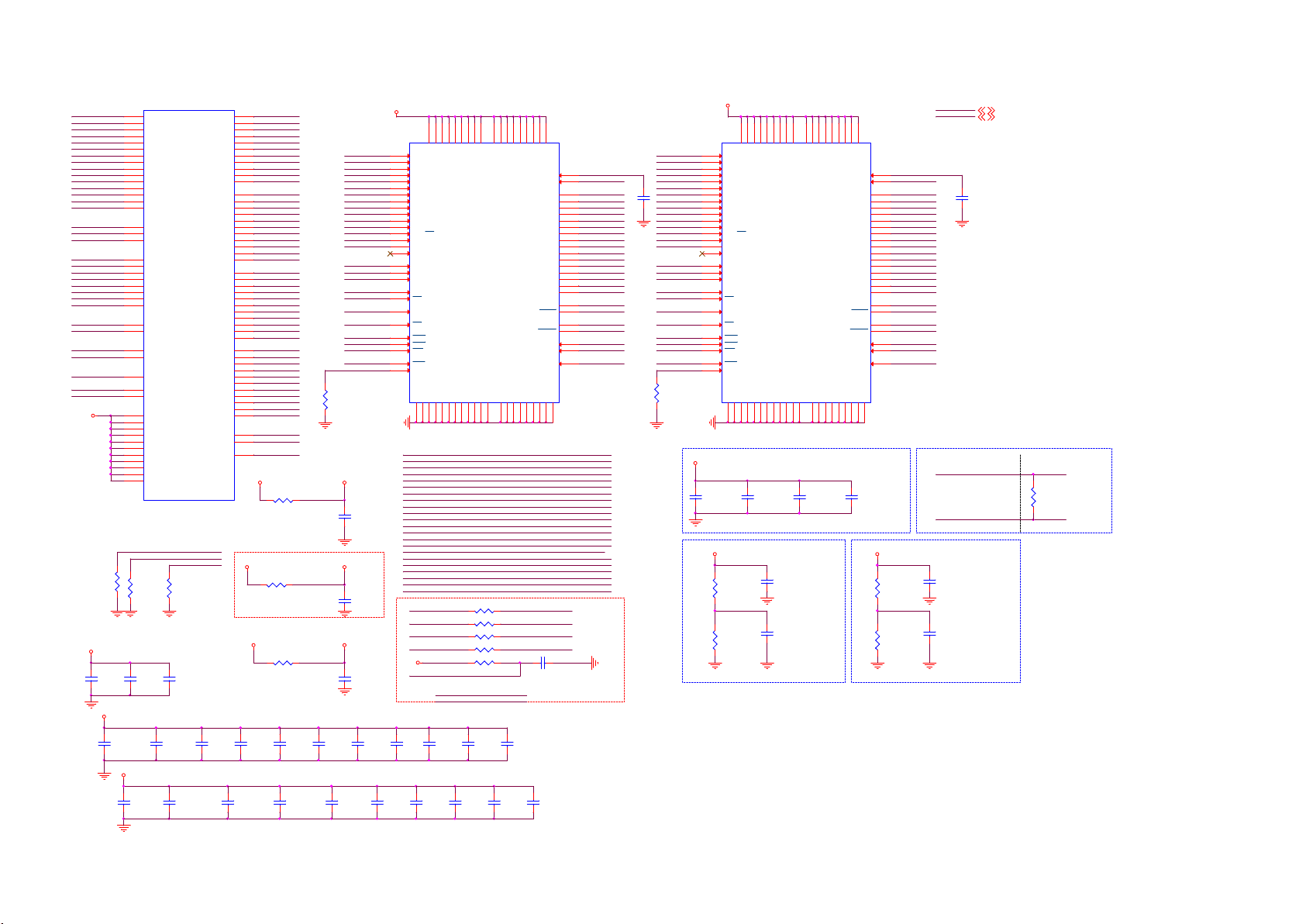
9-5-5 DDR3x2
ARA0
ARA1
ARA2
ARA3
ARA4
ARA5
ARA6
ARA7
ARA8
ARA9
ARA10
ARA11
ARA12
ARA13
ARA14
ARBA0
ARBA1
ARBA2
ARCS
ARCSD
ARRAS#
ARCAS#
ARWE#
ARODT
ARCKE
ARRESET#
ARCLK0
ARCLK0#
DDRVR EF_A1
DDRVR EF_A2
ARTN
MEMTN
MEMTP
DDRV
R450
47R 1/16W 5%
DDRV
C4063
100N 16V
DDRV
R5
ARA0
AB6
ARA1
W7
ARA2
Y6
ARA3
AC6
ARA4
R7
ARA5
AD6
ARA6
T5
ARA7
Y5
ARA8
U5
ARA9
AC7
ARA10
AA5
ARA11
AC5
ARA12
R6
ARA13
U7
ARA14
AB5
ARBA0
AD5
ARBA1
P6
ARBA2
N2
ARCS
N3
ARCSD
N6
ARRAS
P7
ARCAS
AA6
ARWE
N4
ARODT
U6
ARCKE
V6
ARRESET#
M2
ARCLK
M1
ARCLK#
L3
DDRVR EF_A1
AL1
DDRVR EF_A2
N8
ARTN
AB12
MEMTN
AA12
MEMTP
AK4
DDRV
AJ5
DDRV
AK5
DDRV
AH6
DDRV
AJ6
DDRV
AG7
DDRV
AH7
DDRV
AF8
DDRV
V9
DDRV
W9
DDRV
U9
DDRV_C KA
MT5802UHOJ
R474
NC/47R 1/16W 5%
C4067
100N 16V
AVDD10_DD R
AVDD10_DD R
AVDD33_DD R
MEMTN
R473
NC/ 47R 1/16W 5%
C4066
100N 16V
N5
ARDQM0
ARDQS0#
ARDQM1
ARDQS1#
ARDQM2
ARDQS2#
ARDQM3
ARDQS3#
ARTN
MEMTP
ARDQS0
ARDQ0
ARDQ1
ARDQ2
ARDQ3
ARDQ4
ARDQ5
ARDQ6
ARDQ7
ARDQS1
ARDQ8
ARDQ9
ARDQ10
ARDQ11
ARDQ12
ARDQ13
ARDQ14
ARDQ15
ARDQS2
ARDQ16
ARDQ17
ARDQ18
ARDQ19
ARDQ20
ARDQ21
ARDQ22
ARDQ23
ARDQS3
ARDQ24
ARDQ25
ARDQ26
ARDQ27
ARDQ28
ARDQ29
ARDQ30
ARDQ31
ARDQM0
V1
ARDQS0
V2
ARDQS0#
R2
ARDQ0
AB2
ARDQ1
R1
ARDQ2
AB3
ARDQ3
P1
ARDQ4
AC3
ARDQ5
P3
ARDQ6
AC1
ARDQ7
N7
ARDQM1
W2
ARDQS1
W3
ARDQS1#
Y3
ARDQ8
T3
ARDQ9
AA2
ARDQ10
T2
ARDQ11
Y1
ARDQ12
U1
ARDQ13
AA1
ARDQ14
U3
ARDQ15
AG4
ARDQM2
AH2
ARDQS2
AH3
ARDQS2#
AE3
ARDQ16
AL2
ARDQ17
AE2
ARDQ18
AM1
ARDQ19
AD1
ARDQ20
AM2
ARDQ21
AD2
ARDQ22
AL3
ARDQ23
AF5
ARDQM3
AJ1
ARDQS3
AK3
ARDQS3#
AJ3
ARDQ24
AF3
ARDQ25
AK2
ARDQ26
AF1
ARDQ27
AG5
ARDQ28
AG1
ARDQ29
AK1
ARDQ30
AG2
ARDQ31
AD18
AVDD10_DD R
AD19
AVDD10_DD R
L1
AVDD33_DD R
R471
NC/ 0R05 1/16W
Reseved only
Place bottom layer and close to U401
VCCK
R465 0R05 1/16W
R470
0R05 1/16W
U401-1
DRAM#1 Bypass Cap
C4120
C4053
C4118
10uF 6.3V
DDRV
NC/ 10uF 6.3V
100N 16V
C4054
100N 16V
DRAM#2 Bypass Cap
C4060
10uF 6.3V
C4121
NC/ 10uF 6.3V
C4065
100N 16V
AVDD10_DD R
C4055
100N 16V
C4116
100N 16V
AVDD10_DD R
AVDD33_DD R
C4119
100N 16V
DDR3#1
1_A01_A0
1_A11_A1
1_A21_A2
1_A31_A3
1_A41_A4
1_A51_A5
1_A61_A6
1_A71_A7
1_A81_A8
1_A91_A9
1_A101_A10
1_A111_A11
1_A121_A12
1_A13
1_A14
1_BA01_BA0
1_BA11_BA1
1_BA21_BA2
ARCLK0ARCLK0
ARCLK0#ARC LK0B
1_CKE1_C KE
1_ARCS1_ARCS
1_RAS#1 _RAS#
1_CAS#1 _CAS#
1_WE#1_WE#
1_RREST_MEM
A_ZQ1
R421
240R 1%
AVDD10_DD RVCCK
C4185
100N 16V
AVDD10_DD R
C4176
NC/ 1uF 10V
AVDD33_DD RDVDD3V3
C4177
1UF 6. 3V
C4056
100N 16V
C4068
100N 16V
DDRV
VDDB2VDDD9VDDG7VDDK2VDDK8VDDN1VDDN9VDDR1VDD
ARA101_A10 2_A10
ARBA11_BA1 2_BA1
ARA121_A12 2_A12
ARA131_A13 2_A13
ARA91_A9 2_A9
ARA61_A6 2_A6
ARA81_A8 2_A8
ARA111_A11 2_A11
ARBA21_BA2 2_BA2
ARA51_A5 2_A5
ARBA01_BA0 2_BA0
ARA31_A3 2_A3
ARWE#1_WE# 2_W E#
R436
R437
R428
R448
R444
NC/ 47K 1% 1/16W
C4058
C4059
100N 16V
100N 16V
C4071
100N 16V
R9
VDDQA1VDDQA8VDDQC1VDDQC9VDDQD2VDDQE9VDDQF1VDDQH2VDDQ
NC/0R 05 1/16W
NC/0R 05 1/16W
47R 1/16W 5%
47R 1/16W 5%
1_ARCSARCS
2_ARCSDARCSD
C4072
100N 16V
N3
A0
P7
A1
P3
A2
N2
A3
P8
A4
P2
A5
R8
A6
R2
A7
T8
A8
R3
A9
L7
A10/AP
R7
A11
N7
A12/BC
T3
A13
T7
A14
M7
NC_A15
M2
BA0
N8
BA1
M3
BA2
J7
CK
K7
CK
K9
CKE
L2
CS
J3
RAS
K3
CAS
L3
WE
T2
RST
L8
ZQ
VSSA9VSSB3VSSE1VSSG8VSSJ2VSSJ8VSSM1VSSM9VSSP1VSSP9VSST1VSST9VSSQB1VSSQB9VSSQD1VSSQD8VSSQE2VSSQE8VSSQF9VSSQG1VSSQ
CH1 AD/CM
1_A4 AR A4 2_A4
1_A7 AR A7 2_A7
1_RREST_MEM ARRESET# 2_RREST_MEM
1_A1 AR A1 2_A1
1_CAS# AR CAS# 2_CAS#
1_A0 AR A0 2_A0
1_A14 ARA14 2_A14
1_RAS# AR RAS# 2_RAS#
1_A2 AR A2 2_A2
DDRVR EF_A1 A_VREFC A1
ARCKE 1_CKE
ARODT 1_ODT 2_ODT
DDRV
ARRESET#
C4057
100N 16V
C4069
C4070
100N 16V
100N 16V
C4109
100N 16V
H9
VREF_DQ
VREF_CA
DQL0
DQL1
DQL2
DQL3
DQL4
DQL5
DQL6
DQL7
DQU0
DQU1
DQU2
DQU3
DQU4
DQU5
DQU6
DQU7
LDQS
LDQS
UDQS
UDQS
LDM
UDM
ODT
A_VREFCA2DDRVR EF_A2
C4117
100N 16V
U402
K4B4G1646E-BCMA
H1
M8
E3
F7
F2
F8
H3
H8
G2
H7
D7
C3
C8
C2
A7
A2
B8
A3
F3
G3
C7
B7
E7
D3
K1
G9
2_CKE
C4113
NC/ 100NF 16V
DDRVR EF_A1
A_VREFCA1
ARDQ0
ARDQ1
ARDQ2
ARDQ3
ARDQ4
ARDQ5
ARDQ6
ARDQ7
ARDQ8
ARDQ9
ARDQ10
ARDQ11
ARDQ12
ARDQ13
ARDQ14
ARDQ15
ARDQS0
ARDQS0#
ARDQS1
ARDQS1#
ARDQM0
ARDQM1
1_ODT1_ODT
DDR3#2
2_A02_A0
2_A12_A1
2_A22_A2
2_A32_A3
2_A42_A4
2_A52_A5
2_A62_A6
2_A72_A7
C4087
2_A82_A8
100N 16V
2_A92_A9
2_A102_A10
2_A112_A11
2_A122_A12
2_A132_A13
2_A142_A14
2_BA02_BA0
2_BA12_BA1
2_BA22_BA2
ARCLK0ARCLK0
ARCLK0#ARC LK0B
2_CKE2_C KE
2_ARCSD2_ARCSD
2_RAS#2_R AS#
2_CAS#2_C AS#
2_WE#2_WE#
2_RREST_MEM
A_ZQ2
R422
240R 1%
DDRV
DDRV
VDDB2VDDD9VDDG7VDDK2VDDK8VDDN1VDDN9VDDR1VDD
R9
VDDQA1VDDQA8VDDQC1VDDQC9VDDQD2VDDQE9VDDQF1VDDQH2VDDQ
N3
A0
P7
A1
P3
A2
N2
A3
P8
A4
P2
A5
R8
A6
R2
A7
T8
A8
R3
A9
L7
A10/AP
R7
A11
N7
A12/BC
T3
A13
T7
A14
M7
NC_A15
M2
BA0
N8
BA1
M3
BA2
J7
CK
K7
CK
K9
CKE
L2
CS
J3
RAS
K3
CAS
L3
WE
T2
RST
L8
ZQ
VSSA9VSSB3VSSE1VSSG8VSSJ2VSSJ8VSSM1VSSM9VSSP1VSSP9VSST1VSST9VSSQB1VSSQB9VSSQD1VSSQD8VSSQE2VSSQE8VSSQF9VSSQG1VSSQ
H9
VREF_DQ
VREF_CA
DQL0
DQL1
DQL2
DQL3
DQL4
DQL5
DQL6
DQL7
DQU0
DQU1
DQU2
DQU3
DQU4
DQU5
DQU6
DQU7
LDQS
LDQS
UDQS
UDQS
LDM
UDM
ODT
G9
DRAM#1/2 Bottom Layer
C4080
NC/100N F 16V
C4082
NC/100N F 16V
DDRV
DDR3#1 Ref Volt.
R424
1K 1/16W 5%
A_VREFCA1 A_VREFCA2
R426
1K 1/16W 5%
C4051
100N 16V
C4062
100N 16V
C4079
NC/100N F 16V
Near DRAM
C4081
NC/100N F 16V
DDRV
DVDD3V3
VCCK
U403
K4B4G1646E-BCMA
H1
DDRVREF _A2
M8
A_VREFCA2
E3
ARDQ16
F7
ARDQ17
F2
ARDQ18
F8
ARDQ19
H3
ARDQ20
H8
ARDQ21
G2
ARDQ22
H7
ARDQ23
D7
ARDQ24
C3
ARDQ25
C8
ARDQ26
C2
ARDQ27
A7
ARDQ28
A2
ARDQ29
B8
ARDQ30
A3
ARDQ31
F3
ARDQS2
G3
ARDQS2#
C7
ARDQS3
B7
ARDQS3#
E7
ARDQM2
D3
ARDQM3
K1
2_ODT2_ODT
C4088
100N 16V
Differential Clock
NEAR Main Chip
ARCLK0
ARCLK0B
DDR3#2 Ref Volt.
R425
1K 1/16W 5 %
R427
1K 1/16W 5 %
C4052
100N 16V
C4064
100N 16V
Near DRAM
DVDD3V3
VCCK
4,5,6,9, 10,11,14,15,16,17, 19
5,6,17
NEAR DRAM
ARCLK0ARCLK0
R423
100R 1/16W 1%
ARCLK0B
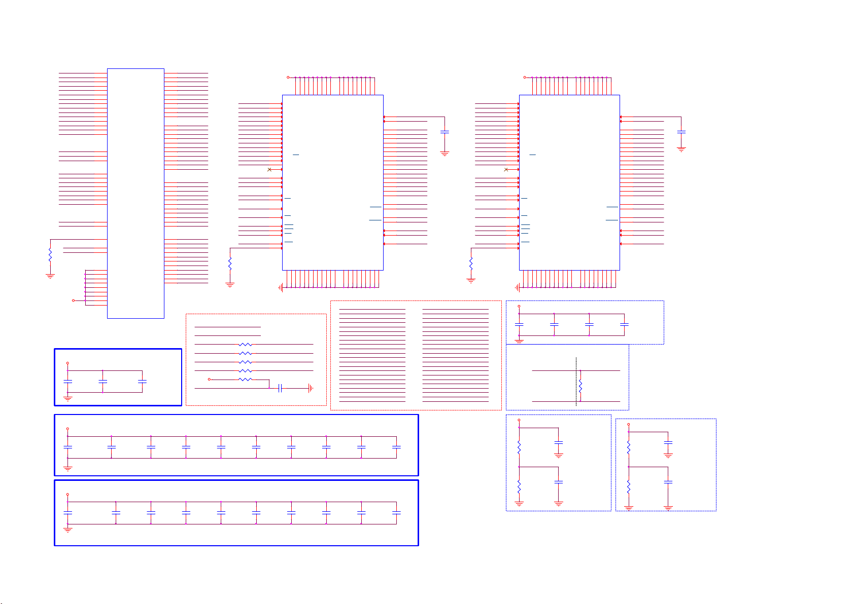
9-5-6 DDR3x2-2
BRA0
BRA1
BRA2
BRA3
BRA4
BRA5
BRA6
BRA7
BRA8
BRA9
BRA10
BRA11
BRA12
BRA13
BRA14
BRBA0
BRBA1
BRBA2
BRCS
BRCSD
BRRAS#
BRCAS#
BRWE#
BRODT
BRCKE
BRRESET#
BRCLK0
BRCLK0#
DDRVR EF_B1
DDRVR EF_B2
R447
47R 1/16W 5%
DDRV
DDRV
AH9
AH17
AJ14
AJ16
AH19
AG9
AJ19
AH11
AG17
AH13
AG21
AH18
AJ20
AJ11
AJ13
AJ17
AH20
AK9
AK6
AK7
AJ10
AH16
AK12
AH14
AM5
AG19
BRTN
AN2
AL23
AE12
AE11
AE10
AD10
AE9
AD9
AC9
AB9
AE15
DRAM#3/4 Bypass Cap
C4073
100N 16V
AJ8
AJ7
AL6
U401-2
BRA0
BRA1
BRA2
BRA3
BRA4
BRA5
BRA6
BRA7
BRA8
BRA9
BRA10
BRA11
BRA12
BRA13
BRA14
BRBA0
BRBA1
BRBA2
BRCS
BRCSD
BRRAS
BRCAS
BRWE
BRODT
BRCKE
BRRESET#
BRCLK
BRCLK#
BRTN
DDRVR EF_B1
DDRVR EF_B2
DDRV
DDRV
DDRV
DDRV
DDRV
DDRV
DDRV
DDRV
DDRV_ CKB
MT5802UHOJ
C4074
100N 16V
BRDQM0
BRDQS0
BRDQS0#
BRDQ0
BRDQ1
BRDQ2
BRDQ3
BRDQ4
BRDQ5
BRDQ6
BRDQ7
BRDQM1
BRDQS1
BRDQS1#
BRDQ8
BRDQ9
BRDQ10
BRDQ11
BRDQ12
BRDQ13
BRDQ14
BRDQ15
BRDQM2
BRDQS2
BRDQS2#
BRDQ16
BRDQ17
BRDQ18
BRDQ19
BRDQ20
BRDQ21
BRDQ22
BRDQ23
BRDQM3
BRDQS3
BRDQS3#
BRDQ24
BRDQ25
BRDQ26
BRDQ27
BRDQ28
BRDQ29
BRDQ30
BRDQ31
C4078
100N 16V
AM6
BRDQM0
AL9
BRDQS0
AM9
BRDQS0#
AM4
BRDQ0
AM13
AN4
AN13
AM3
AN14
AN3
AL14
AN5
AM10
AN10
AN11
AN7
AM12
AM7
AL11
AL8
AL12
AN8
AH21
AM19
AN19
AN16
AM22
AM16
AN22
AL15
AM23
AM15
AN23
AK21
AL20
AN20
AH22
AN17
AM21
AL17
AJ22
AL18
AL21
AM18
BRDQ1
BRDQ2
BRDQ3
BRDQ4
BRDQ5
BRDQ6
BRDQ7
BRDQM1
BRDQS1
BRDQS1#
BRDQ8
BRDQ9
BRDQ10
BRDQ11
BRDQ12
BRDQ13
BRDQ14
BRDQ15
BRDQM2
BRDQS2
BRDQS2#
BRDQ16
BRDQ17
BRDQ18
BRDQ19
BRDQ20
BRDQ21
BRDQ22
BRDQ23
BRDQM3
BRDQS3
BRDQS3#
BRDQ24
BRDQ25
BRDQ26
BRDQ27
BRDQ28
BRDQ29
BRDQ30
BRDQ31
DDR3#3
3_RREST_MEM
B_ZQ1
R434
240R 1%
3_ARCSBRC S
DDRVR EF_B1 B_VREFCA1
DDRVR EF_B2
BRCKE 3_CKE 4_CKE
DDRV
BRRESET#
4_ARCSDBRCSD
R438 NC/ 0R05 1/16W
R439 NC/ 0R05 1/16W
R429 47R 1/ 16W 5%
3_ODTBRODT 4_ODT
R449 47R 1/ 16W 5%
R446 NC/ 47K 1% 1/16W
3_A0
3_A1
3_A2
3_A3
3_A4
3_A5
3_A6
3_A7
3_A8
3_A9
3_A10
3_A11
3_A12
3_A13
3_A14
3_BA0
3_BA1
3_BA2
BRCLK0
BRCLK0#
3_CKE
3_ARCS
3_RAS#
3_CAS#
3_WE#
C4114 NC/100NF 16V
DDRV
N3
A0
VDDB2VDDD9VDDG7VDDK2VDDK8VDDN1VDDN9VDDR1VDD
P7
A1
P3
A2
N2
A3
P8
A4
P2
A5
R8
A6
R2
A7
T8
A8
R3
A9
L7
A10/AP
R7
A11
N7
A12/BC
T3
A13
T7
A14
M7
NC_A15
M2
BA0
N8
BA1
M3
BA2
J7
CK
K7
CK
K9
CKE
L2
CS
J3
RAS
K3
CAS
L3
WE
T2
RST
L8
ZQ
VSSA9VSSB3VSSE1VSSG8VSSJ2VSSJ8VSSM1VSSM9VSSP1VSSP9VSST1VSST9VSSQB1VSSQB9VSSQD1VSSQD8VSSQE2VSSQE8VSSQF9VSSQG1VSSQ
B_VREFCA2
R9
VDDQA1VDDQA8VDDQC1VDDQC9VDDQD2VDDQE9VDDQF1VDDQH2VDDQ
3_A2 BRA2
3_BA0 BRBA0
3_A3 BRA3
3_WE# BRWE#
3_A14 BRA14
3_RAS# BRRAS#
3_CAS# BRCAS#
3_BA2 BRBA2
3_A0 BRA0
3_A5 BRA5
3_A6 BRA6
3_A1 BRA1
3_A8 BRA8
3_A11 BRA11
3_A10 BRA10
3_BA1 BRBA1
3_A12 BRA12
3_A4 BRA4
3_A7 BRA7
3_A13 BRA13
3_A9 BRA9
3_RREST_MEM BR RESET#
H9
VREF_DQ
VREF_CA
DQL0
DQL1
DQL2
DQL3
DQL4
DQL5
DQL6
DQL7
DQU0
DQU1
DQU2
DQU3
DQU4
DQU5
DQU6
DQU7
LDQS
LDQS
UDQS
UDQS
LDM
UDM
ODT
U404
K4B4G1646E-BCMA
H1
M8
E3
F7
F2
F8
H3
H8
G2
H7
D7
C3
C8
C2
A7
A2
B8
A3
F3
G3
C7
B7
E7
D3
K1
G9
DDRVR EF_B1
B_VREFCA1
BRDQ0
BRDQ1
BRDQ2
BRDQ3
BRDQ4
BRDQ5
BRDQ6
BRDQ7
BRDQ8
BRDQ9
BRDQ10
BRDQ11
BRDQ12
BRDQ13
BRDQ14
BRDQ15
BRDQS0
BRDQS0#
BRDQS1
BRDQS1#
BRDQM0
BRDQM1
3_ODT
4_A2 BRA2
4_BA0 BRBA0
4_A3 BRA3
4_WE# BRWE#
4_A14 BRA14
4_RAS# BRRAS#
4_CAS# BRCAS#
4_BA2 BRBA2
4_A0 BRA0
4_A5 BRA5
4_A6 BRA6
4_A1 BRA1
4_A8 BRA8
4_A11 BRA11
4_A10 BRA10
4_BA1 BRBA1
4_A12 BRA12
4_A4 BRA4
4_A7 BRA7
4_A13 BRA13
4_A9 BRA9
4_RREST_MEM BRR ESET#
C4089
100N 16V
DDR3#4
4_A0
4_A1
4_A2
4_A3
4_A4
4_A5
4_A6
4_A7
4_A8
4_A9
4_A10
4_A11
4_A12
4_A13
4_A14
4_BA0
4_BA1
4_BA2
BRCLK0
BRCLK0#
4_CKE
4_ARCSD
4_RAS#
4_CAS#
4_WE#
4_RREST_MEM
B_ZQ2
R435
240R 1%
DDRV
N3
A0
VDDB2VDDD9VDDG7VDDK2VDDK8VDDN1VDDN9VDDR1VDD
P7
A1
P3
A2
N2
A3
P8
A4
P2
A5
R8
A6
R2
A7
T8
A8
R3
A9
L7
A10/AP
R7
A11
N7
A12/BC
T3
A13
T7
A14
M7
NC_A15
M2
BA0
N8
BA1
M3
BA2
J7
CK
K7
CK
K9
CKE
L2
CS
J3
RAS
K3
CAS
L3
WE
T2
RST
L8
ZQ
VSSA9VSSB3VSSE1VSSG8VSSJ2VSSJ8VSSM1VSSM9VSSP1VSSP9VSST1VSST9VSSQB1VSSQB9VSSQD1VSSQD8VSSQE2VSSQE8VSSQF9VSSQG1VSSQ
DDRV
DRAM#3/4 Bottom Layer
C4075
NC/100N F 16V
R9
VDDQA1VDDQA8VDDQC1VDDQC9VDDQD2VDDQE9VDDQF1VDDQH2VDDQ
C4077
NC/100N F 16V
Damping and Termina tion for CLK
Close to MainChip
BRCLK0
BRCLK0#
Close to DRAM
R476
100R 1/16W 1%
H9
VREF_DQ
VREF_CA
DQL0
DQL1
DQL2
DQL3
DQL4
DQL5
DQL6
DQL7
DQU0
DQU1
DQU2
DQU3
DQU4
DQU5
DQU6
DQU7
LDQS
LDQS
UDQS
UDQS
LDM
UDM
ODT
G9
C4076
NC/100N F 16V
BRCLK0
BRCLK0#
U405
K4B4G1646E-BCMA
H1
DDRVR EF_B2
M8
B_VREFCA2
E3
BRDQ16
F7
BRDQ17
F2
BRDQ18
F8
BRDQ19
H3
BRDQ20
H8
BRDQ21
G2
BRDQ22
H7
BRDQ23
D7
BRDQ24
C3
BRDQ25
C8
BRDQ26
C2
BRDQ27
A7
BRDQ28
A2
BRDQ29
B8
BRDQ30
A3
BRDQ31
F3
BRDQS2
G3
BRDQS2#
C7
BRDQS3
B7
BRDQS3#
E7
BRDQM2
D3
BRDQM3
K1
4_ODT
C4061
NC/100N F 16V
C4090
100N 16V
DDRV
DDRV
C4122
10uF 6.3V
C4100
10uF 6.3V
C4125
10uF 6. 3V
C4126
10uF 6. 3V
DRAM#3 Bypass Cap
C4084
100N 16V
DRAM#4 Bypass Cap
C4103
100N 16V
C4097
100N 16V
C4105
100N 16V
C4102
100N 16V
C4112
100N 16V
C4123
100N 16V
C4101
100N 16V
C4085
100N 16V
C4104
100N 16V
C4108
100N 16V
C4107
100N 16V
C4086
100N 16V
C4106
100N 16V
C4110
100N 16V
C4111
100N 16V
DDRV
DDR3#3 Ref Vol t.
R430
1K 1/16W 5%
B_VREFCA1
R433
1K 1/16W 5%
C4173
100N 16V
C4083
100N 16V
DDRV
DDR3#4 Ref Vol t.
R431
1K 1/16W 5%
B_VREFCA2
R432
1K 1/16W 5%
C4181
100N 16V
C4096
100N 16V
Near DRAMNear DRAM

9-5-7 YPbPr/CVBS
R164
1K2 OHM
Tun er/DEMOD
DVDD3V3
ADCIN P_DEMOD
ADCIN N_DEMOD
R161
1K2 OHM
TP109
OSCL2
OSDA2
DISEQC_I N
DISEQC_OU T
TP5454
DVBS2_SIF_I P
DVBS2_SIF_QP
TP5455
TP5456 C4197
AVDD33_VID EO_STB
AVDD33_DEMOD_STB
AVDD33_DTMB
DVDD1V2_D TMB
AVDD1V2_DTMB
AVSS33_DEMOD
Close to Main Chip
IF_AGC
IF_AGC
R166
10K 1/16W 5%
U401-5
A31
ADCIN P_DEMOD
B31
ADCIN N_DEMOD
C9
IF_AGC
D9
RF_AGC
E14
OSCL2
F14
OSDA2
D31
DISEQC_I N
D30
DISEQC_OU T
B33
DVBS2_SIFIP
B32
DVBS2_SIFQP
J24
AVDD33_VID EO_STB
J25
AVDD33_DEMOD_STB
L20
AVDD33_DEMODE
AM24
DVDD12_D EMODE
AN24
DVDD12_D EMODE
AJ23
AVDD12_DEMODE
L22
AVSS33_DEMOD
MT5802UHOJ
IF_AGCT
C120
47NF 16V
H31
TP_H
J32
TP_V
K32
J31
F31
F32
E31
E32
E33
H32
H33
G31
G33
G32
C33
D32
C32
E30
PD_TX
PD_RX
SOY0
Y0P
COM0
PB0P
PR0P
CVBS0P
CVBS_COM
R5168
10R 1/16W 5%
3V3SB
R478
0R05 1/16W
AVDD33_VID EO_STB
TUNER_BY PASS_OUT
Analog Power
AVDD33_DEMOD_STB
C4156
10uF 6.3V
R1004
NC/75 OHM +-5% 1/16W
AVDD3V3
C4191
NC/100N 16V
AVDD33_DTMB
NC/10N 50V
C4179
100N 16V
AVDD1V2
AVDD1V2_DTMB
C4188
NC/10N 50V
C4198
100N 16V
C4189
10UF 6. 3V 20%
U1TX
U1RX
SOY0
Y0P
COM0
PB0P
PR0P
SOY1
Y1P
COM1
PB1P
PR1P
CVBS0P
CVBS1P
CVBS_COM
VDACX_OUT
Close to Main Chip
AVDD1V2
DVDD1V2_D TMB
13
13
C4196
100N 16V
C4195
10UF 6. 3V 20%
3V3SB
13
PD_TX
PD_RX
R8158
R8159
3.3K 1/16W
3.3K 1/16W
ADCIN P_DEMOD
Close to Main Chip
R126
R128
0R05 1/16W
0R05 1/16W
C1046
NC/ 47pF 50V
TU_FAT_IN2+
TU_FAT_IN2-ADCIN N_DEMOD
C1047
NC/ 47pF 50V
TU_FAT_IN2+
TU_FAT_IN2-
AVDD3V3
3V3SB
+5V_SW
+5V_STB
AVDD1V2
DVDD3V3
AIN_R0
AIN_L0
OSCL2
OSDA2
PD_TX
PD_RX
AVDD3V3
3V3SB
+5V_SW
+5V_STB
AVDD1V2
DVDD3V3
OSCL2
OSDA2
AIN_R0
AIN_L0
PD_TX
PD_RX
5,11,12,16, 19
4,5,6,12, 14,16,20
5,12,13,19, 20,24,29
4,5,12,14, 16
5
4,5,6,7, 10,11,14,16,17,19
10
10
19
19
Rear YPbPr /CVBS + R/L
CN101
G/Y
B
R
W
R
R
W
Y
NC/R CA 8P
E
D
C
B
A
RCA J ACK 13P
CN102
A
B
C
13
12
11
10
9
8
7
6
5
4
3
2
1
3
2
1
5
4
8
7
6
Y_IN _1
Y_DET
PB_IN_1
PR_IN_1
YPBPR_D ETECT
R8123
NC/0R05 1/10W
When CVBS only
AP
LA
CN102 NC
CN101 NC
wit h GND
R1013 0R05 1/10W
+5V_STB
C109
1uF 10V
12
12
ZD101
ZD106
AZ5123-01H.R 7G
AZ5123-01H.R 7G
12
ZD105
AZ5123-01H.R 7G
YPbPrR_I N
12
ZD104
AZ5123-01H.R 7G
YPbPrL_IN
C1044
1N 50V
12
ZD102
AZ5123-01H.R 7G
12
ZD103
AZ5123-01H.R 7G
C1045
1N 50V
3
D101
R1005
NC/BAV99
1
2
R1008
0R05 1/10W
R1012
0R05 1/10W
C1029 1uF 10V R1139 30K OHM +-1% 1/ 16W
C1030 1uF 10V
75R 1/16W 1%
wit h GND
R1010
75R 1/16W 1%
R1011
75R 1/16W 1%
wi th GND
wi th GND
wi th GND
NEAR YPbPr CONNECTOR
C1034
10PF 50V
C1040
10PF 50V
C1041
10PF 50V
R1001
10R 1/16W 1%
R1002
100R 1/16W 5%
R1003
100R 1/16W 5%
R1007
100R 1/16W 5%
R1009
100R 1/16W 5%
R104
0R05 1/16W
CVBS_COM
wi th GND
R1015
100R 1/16W 5%
wi th GND
R1140 30K OHM +-1% 1/16W
Near Scaler
C1035
1.5nF 50V
C1036
47nF 16V
C1037
10N 50V
C1038
10N 50V
C1039
10N 50V
C1031
1uF 10V
ゲ斗 猽
C1042
10N 50V
SOY0
CVBS0P
Y0P
COM0
PB0P
CVBS_COM
CVBS3PǐCN116
PR0P
AIN_R0
AIN_L0
キ︽絬
ǐ
Source_DET
H:Pr Plug-in (YPbPr)
L:Pr Plug-out (AV)
YPBPR _DETECT
Vedio_DET
H:Pr Plug-in (Cable detect)
L:Pr Plug-out (Non Cable)
Y_D ET
R1016
100R 1/16W 5%
R114
100R 1/16W 5%
DVDD3V3
DVDD3V3
R1017
47K 1/16W 5%
YPBPR_D ETECT1
R106
47K 1/16W 5%
VIDEO_DET
15
15
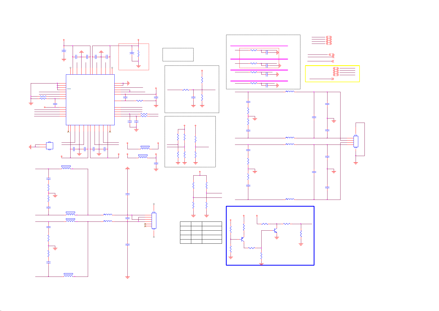
9-5-8 AUDIO AMP
PVDD
C613
C627
100N 16V
PVDD
FB4323 120R 3A
C8187
470pF 50V
R8173
10 OHM
R8174
10 OHM
C8186
470pF 50V
C8182
470pF 50V
R8169
10 OHM
R8168
10 OHM
C8181
470pF 50V
+
C609
C610
100N 50V
100N 50V
LA
LB
45LA46
47NC48
GNDL
VDDLA
49
THERMALPAD
1
SDATA1
2
MS
3
PLL
4
CFG0
5
CFG1
6
CLK_OUT
7
DGND
8
DVDD
9
SDATA0
10
LRCIN
11
BCLK
12
MCLK
NC13VDDS114S1A15GNDS116S1B17VDDS118VDDS219S2B20GNDS221S2A22VDDS223NC
S1A
C8198
C8199
100N 50V
100N 50V
1 2
FB4324 120R 3A
1 2
FB4325 120R 3A
1 2
FB4326 120R 3A
1 2
C611
100N 50V
42
43LB44
VDDLB
VDDRB
C8201
100N 50V
150uF 20% 16V
AD87588-LG48NAY:356G0616048163
AD83586B-LG48NAY:356G0616048602
2.0 CH
INDUCTOR
24V
10uH
AD82588
073G253S 81 Y
12V
15uH
AD83586
373G253S247Y00
2.1 CH
22uH
AD83586
373G253S147Y00
AMP_CFG0
AMP_CFG1
R615 NC/0R05 O HM
R616 0R05 1/10W
AU_VDD3V3
SDI AMP_SA0
LRCLKI
BICKI
MCLK
HS601
1
2
HEAT SINK
S1A
S1B
S2B
S2A
8x10. 2mm (獶IO跋)
C612
100N 50V
RA
RB
37
38RA39
40RB41
GNDR
VDDRA
LINEIN
LREX
RESET#
ERROR#
PD#
DVDD
DGND
DEF
SA1
SA0
SCL
SDA
24
C8200
100N 50V
L4104 10uH
L4105 10uH
C614
150uF 20% 16V
U601
AD83586B-LG48NAY
NC
36
35
34
33
32
31
30
29
28
27
26
A_SCL
25
A_SDA
AU_12V
S2A
S2B
PVDD
DVDD3V3
+
C625
100N 16V
AMP_DEF
AMP_SA1
C632
NC/22P 50V
C8180
100N 50V
C8202
0.47uf 10% 50V
C8185
100N 50V
PVDD
R608
10K 1/4W
RESET#
PWRDN
R617
0R05 1/10W
R620
R621
C633
22R 1/10W 5%
22R 1/10W 5%
NC/22P 50V
FB601
120R 6A
FB602
1 2
120R 3A
10UF 6. 3V 20%
Stereo mode:
FB607, FB610,
C628: NC
Woofer
4 ohm: 10uH, 470nF
6 ohm: 15uH, 470nF
8 ohm: 22uH, 470nF
AU_VDD3V3
OSCL2
OSDA2
PVDD
12
AU_VDD3V3
C602
78
1
2
3
4
5
6
I2SAMP_RESET
Low: reset
High: normal
Reset (p ull-up )
I2SAMP_RESET
C626
22UF
I2C address
Write=0110"SA0"0"SA1"0=0x60
AMP_SA0
AMP_SA1
R
CN603
R-
CONN 6P
R+
LL+
L
R610
0R05 1/16W
R624
R629
10K 1/16W 5%
CFG1
R625
R630
0
1
NC/10K
NC/10K
DVDD3V3DVDD3V3
10K 1/16W 5%
DVDD3V3
C619
1uF 10V
R626
NC/10K 1/16W 5%
AMP_DEF
R631
10K 1/16W 5%
DVDD3V3
R601
0R05 1/16W
R604
NC/0R 05 OHM
CFG0
0
10
01
1
R660
NC/10K 1/16W 5%
RESET#
R609
10K 1/16W 5%
R602
NC/0R 05 1/16W
AMP_CFG0
AMP_CFG1
R605
0R05 1/16W
Mode
Mono
Stereo
2.1CH
2.1CH
For EMI, close to SoC
All Path Grounding(20mil)
AOMCLK
R643
AOBCK
AOLRCK
AOSDATA0
RA
RB
LA
LB
Option
R645
NC/470K
1
R640
NC/180K
47R 1/16W 5%
R603
47R 1/16W 5%
R606
0R05 1/16W
R607
0R05 1/16W
R611
10 OHM
R613
10 OHM
R622
10 OHM
R627
10 OHM
Anti-pop
DVDD3V3
R649
NC/1K
23
Q603
NC/LMBT3906LT1G
R639
NC/0R 05 1/16W
Mo dify by EM I
PVDD
C616
470pF 50V
C623
470pF 50V
C630
470pF 50V
C642
470pF 50V
DVDD3V3
Mo dify by EM I 10/12
MCLK
C603
18pF 50V
BICKI
C605
18pF 50V
LRCLKI
C607
33pF 50V
SDI
C608
33pF 50V
R632
NC/10K
R636
NC/10K
Ground ing
Ground ing
Ground ing
Ground ing
L601
22uH
L603
22uH
L604
22uH
R644
NC/0R 05 1/16W
Q601
NC/MMBT3904
L602
22uH
3V3SB
DVDD3V3
+5V_SW
AU_12V
GPIO & I2 C Control
OSDA2
OSCL2
I2SAMP_RESET
I2S Contr ol
19
AOMCLK
19
AOBCK
19
AOLRCK
19
AOSDATA0
PWRDN
100N 50V
C620
100N 50V
100N 50V
100N 50V
C635
100N 50V
100N 50V
PWRDN
R635
10K
3V3SB
DVDD3V3
+5V_SW
AU_12V
OSDA2
OSCL2
I2SAMP_RESET
PWRDN
C617
C622
C631
C641
4,5,6,9, 12,14,16,20
4,5,6,7, 9,11,14,15,16,17, 19
5,12,13,19, 20,24,29
4
9
9
15
AOMCLK
AOBCK
AOLRCK
AOSDATA0
15,20
Stereo mode:
FB607, FB610,
C628: NC
56
CN601
1
RR+
L-
4 ohm: 10uH, 470nF
6 ohm: 15uH, 470nF
8 ohm: 22uH, 470nF
CONN
2
3
4
L+S1B
R
RR+
LL+
L

9-5-9 VB1 output
MT5802 Vx1 OUTPUT
U401-3
AVDD10_LVDS_STB
AVDD33_LVDSA
AH23
AVDD10_LVDS_STB
K20
AVDD33_LVDSA
MT5802UHOJ
Panel VCC=12V
+12V
FB712
1 2
NC/ 120R 6A
PANEL_PWR_EN
Normal:High
Stand_By:Low
PANEL_VCC_ON/ OFF
RA7629 N C/0R05 OH M
NT-LCD-PWR-ON
RA3335 N C/0R05 OH M
AN28
AE0P
AM28
AE0N
AL27
AE1P
AK27
AE1N
AL26
AE2P
AK26
AE2N
AN26
AECKP
AM26
AECKN
AL25
AE3P
AK25
AE3N
AL24
AE4P
AK24
AE4N
AN32
AO0P
AM32
AO0N
AL31
AO1P
AK31
AO1N
AL30
AO2P
AK30
AO2N
AN30
AOCKP
AM30
AOCKN
AL29
AO3P
AK29
AO3N
AL28
AO4P
AK28
AO4N
R793
NC/10K 1/10W 5%
R799
NC/10K 1/16W 5%
Close to SoC
LVDSTX_AE0P
LVDSTX_AE0N
LVDSTX_AE1P
LVDSTX_AE1N
LVDSTX_AE2P
LVDSTX_AE2N
LVDSTX_AECKP
LVDSTX_AECKN
LVDSTX_AE3P
LVDSTX_AE3N
LVDSTX_AE4P
LVDSTX_AE4N
LVDSTX_AO0P
LVDSTX_AO0N
LVDSTX_AO1P
LVDSTX_AO1N
LVDSTX_AO2P
LVDSTX_AO2N
LVDSTX_AOCKP
LVDSTX_AOCKN
LVDSTX_AO3P
LVDSTX_AO3N
LVDSTX_AO4P
LVDSTX_AO4N
8
7
6
5
C4939 100N 16V
C4940 100N 16V
C4941 100N 16V
C4942 100N 16V
C4943 100N 16V
C4944 100N 16V
C4945 100N 16V
C4946 100N 16V
C4947 100N 16V
C4948 100N 16V
C4949 100N 16V
C4950 100N 16V
C8143 100N 16V
C8144 100N 16V
C8142 100N 16V
C8145 100N 16V
C8147 100N 16V
C8148 100N 16V
C8146 100N 16V
C8149 100N 16V
C4959 100N 16V
C4960 100N 16V
C4961 100N 16V
C4962 100N 16V
Q784
1
D
D
2
D
D
3
D
D
G4S
NC/AON 4421
C788
NC/1U F 10% 16V
R797
NC/6K8 1/10W 5%
R785
NC/5. 1KOHM +-5% 1/10W
Q785
NC/BC 847C
Panel_12V
+
C789
NC/220U F 16V
R4740
NC/10K 1/8W
To CN408
SOC-VB1-TX2p
SOC-VB1-TX2n
SOC-VB1-TX3p
SOC-VB1-TX3n
SOC-VB1-TX4p
SOC-VB1-TX4n
SOC-VB1-TX5p
SOC-VB1-TX5n
SOC-VB1-TX6p
SOC-VB1-TX6n
SOC-VB1-TX7p
SOC-VB1-TX7n
GFX-VB1-TX0p
GFX-VB1-TX0n
GFX-VB1-TX1p
GFX-VB1-TX1n
GFX-VB1-TX2p
GFX-VB1-TX2n
GFX-VB1-TX3p
GFX-VB1-TX3n
SOC-VB1-TX0p
SOC-VB1-TX0n
SOC-VB1-TX1p
SOC-VB1-TX1n
R8163
NC/5. 1KOHM +-5% 1/10W
12
LED301
NC/GPTS06033GC1-PB
Analog Power
DVDD3V3
HTPDn
R1036
NC/10K 5% 1/16W
AGP
R1035
NC/10K 1/16W 5%
C4187
10UF 6. 3V 20%
R4969
NC/ 10K 1/16W 5%
DVDD3V3DVDD3V3
R1043
NC/10K 5% 1/16W
R1037
NC/10K 1/16W 5%
6,11
6,11
C4163
1uF 10V
OSDA0
OSCL0
Bit_SEL
DVDD3V3
R1038
R1042
AVDD3V3AVDD1V0_1
100N 16V
D_Fomat 0
D_Fomat 1
R3207 0R05 1/ 16W
R3208 NC/ 0R05 1/16W
HTPDn
LOCKn
DVDD3V3
R8180
NC/ 10K 1/16W 5%
LOCKn
DVDD3V3
NC/10K 1/16W 5%
D_Fomat 1 Bit_SELD_Fomat 0
NC/ 10K 5% 1/16W
AVDD33_LVDSAAVDD10_LVDS_STB
R3202 NC/ 0R05 1/16W
R3215 NC/ 0R05 1/16W
R3204 NC/ 0R05 1/16W
R3205 NC/ 0R05 1/16W
R3219 0R05 1/ 16W
R3209 0R05 1/ 16W
R3210 0R05 1/ 16W
R1019
NC/10K 1/16W 5%
H or NC = 10bit
L = 8bit
R1040
NC/ 10K 5% 1/16W
C4190
100N 16VC4164
LD_EN
AGP
SOC-VB1-TX0n
SOC-VB1-TX0p
SOC-VB1-TX1n
SOC-VB1-TX1p
SOC-VB1-TX2n
SOC-VB1-TX2p
SOC-VB1-TX3n
SOC-VB1-TX3p
SOC-VB1-TX4n
SOC-VB1-TX4p
SOC-VB1-TX5n
SOC-VB1-TX5p
SOC-VB1-TX6n
SOC-VB1-TX6p
SOC-VB1-TX7n
SOC-VB1-TX7p
Panel_12V
SOC-VB1-TX0n
SOC-VB1-TX0p
SOC-VB1-TX1n
AVDD3V3
DVDD3V3
AVDD1V0_1
SOC-VB1-TX1p
SOC-VB1-TX2n
SOC-VB1-TX2p
SOC-VB1-TX3n
SOC-VB1-TX3p
SOC-VB1-TX4n
SOC-VB1-TX4p
SOC-VB1-TX5n
SOC-VB1-TX5p
SOC-VB1-TX6n
SOC-VB1-TX6p
SOC-VB1-TX7n
SOC-VB1-TX7p
HTPDn
LOCKn
6,11
6,11
GFX-VB1-TX0p
GFX-VB1-TX0n
GFX-VB1-TX1p
GFX-VB1-TX1n
GFX-VB1-TX2p
GFX-VB1-TX2n
GFX-VB1-TX3p
GFX-VB1-TX3n
PANEL_VCC_ON/ OFF
NT-LCD-PWR-ON
CN408
NC/ CONN 51P
51
50
49
48
47
46
45
44
43
42
41
40
39
38
37
36
35
34
33
32
31
30
29
28
27
26
25
24
23
22
21
20
19
18
17
16
15
14
13
12
11
10
9
8
7
6
5
4
3
2
1
52 53
OSDA0
OSCL0
SOC-VB1-TX0n
SOC-VB1-TX0p
SOC-VB1-TX1n
SOC-VB1-TX1p
SOC-VB1-TX2n
SOC-VB1-TX2p
SOC-VB1-TX3n
SOC-VB1-TX3p
SOC-VB1-TX4n
SOC-VB1-TX4p
SOC-VB1-TX5n
SOC-VB1-TX5p
SOC-VB1-TX6n
SOC-VB1-TX6p
SOC-VB1-TX7n
SOC-VB1-TX7p
HTPDn
LOCKn
GFX-VB1-TX0p
GFX-VB1-TX0n
GFX-VB1-TX1p
GFX-VB1-TX1n
GFX-VB1-TX2p
GFX-VB1-TX2n
GFX-VB1-TX3p
GFX-VB1-TX3n
PANEL_VCC_ON/ OFF15
NT-LCD-PWR -ON 4, 24
AVDD3V3
DVDD3V3
AVDD1V0_1
OSDA0
OSCL0
5,9,12,16, 19
4,5,6,7, 9,10,15,16,17,19
4,12
25
25
25
25
25
25
25
25
25
25
25
25
25
25
25
25
19,25
15,25
25
25
25
25
25
25
25
25
MT5802 HEAT SINK
HS401
1
2
HEAT SINK
X90G201003000000SY
筁狾础
12/8 EMI solution
R306
R305
22 OHM 1/10W
22 OHM 1/10W

9-5-10 HDMI/MHL
R501
100R 1/16W 5%
G17
E18
F18
D18
E19
F19
F23
F21
G19
G21
E23
F22
E22
E21
E27
B17
K24
J19
J20
HDMI_CEC CEC
MHL_SENSE
HDMI_0_PWR5V
HDMI_0_HPD_C BUS
HDMI_0_SCL
HDMI_0_SDA
HDMI_1_PWR5V
HDMI_1_HPD
HDMI_1_SCL
HDMI_1_SDA
HDMI_2_PWR5V
HDMI_2_HPD
HDMI_2_SCL
HDMI_2_SDA
AVDD10_ECBUS_STB
AVDD10_HDMI_STB
AVDD33_ECBUS_STB
AVDD33_HDMI
AVDD33_HDMI
U401-6
HDMI_CEC_1
MHL_SENSE
HDMI_0_PWR5V
HDMI_0_HPD_C BUS
HDMI_0_SCL
HDMI_0_SDA
HDMI_1_PWR5V
HDMI_1_HPD
HDMI_1_SCL
HDMI_1_SDA
HDMI_2_PWR5V
HDMI_2_HPD
HDMI_2_SCL
HDMI_2_SDA
AVDD10_ECBUS_STB
AVDD10_HDMI_STB
AVDD33_ECBUS_STB
AVDD33_HDMI
AVDD33_HDMI
HDMI_0_RX_0
HDMI_0_RX_0B
HDMI_0_RX_1
HDMI_0_RX_1B
HDMI_0_RX_2
HDMI_0_RX_2B
HDMI_0_RX_C
HDMI_0_RX_CB
HDMI_1_RX_0
HDMI_1_RX_0B
HDMI_1_RX_1
HDMI_1_RX_1B
HDMI_1_RX_2
HDMI_1_RX_2B
HDMI_1_RX_C
HDMI_1_RX_CB
HDMI_2_RX_0
HDMI_2_RX_0B
HDMI_2_RX_1
HDMI_2_RX_1B
HDMI_2_RX_2
HDMI_2_RX_2B
HDMI_2_RX_C
HDMI_2_RX_CB
C4180
100N 16V
AVDD1V0_1
AVDD10_HDMI_STB
C4192
100N 16V
AVDD1V0_STB
AVDD10_ECBUS_STB
3V3SB
AVDD3V3
R507 0R05 1/16W
C4178
1uF 10V
C4183
10UF
AVDD33_ECBUS_STB
C4155
100N 16V
AVDD3V3_HDMI
Audio Return Chan nel (ARC)
ARC_HDMI
+5V_SW
R577
47K 1/16W 5%
R579
47K 1/16W 5%
C505
1uF 10V
from Scaler ARC
R530
180R
R529
82R
with GND
19
ARC
A15
RX_0_0
B15
RX_0_0B
C14
RX_0_1
D14
RX_0_1B
A13
RX_0_2
B13
RX_0_2B
C16
RX_0_C
D16
RX_0_CB
B20
RX_1_0
A20
RX_1_0B
C19
RX_1_1
D19
RX_1_1B
B18
RX_1_2
A18
RX_1_2B
D21
RX_1_C
C21
RX_1_CB
B24
RX_2_0
A24
RX_2_0B
D23
RX_2_1
C23
RX_2_1B
B22
RX_2_2
A22
RX_2_2B
D25
RX_2_C
C25
RX_2_CB
Analog Power
AVDD3V3_HDMI
+5V_SW
R553
1K 1/16W 5%
C501
10NF 50V
AVDD33_HDMI
Q509
AO3414
R506
100K 1/16W 5%
Prevent HDMI leakage from HDMI device.
CEC
HDMI_CEC
C506
6.8PF 50V
with GND
R505 0R05 1/16W
R504 0R05 1/16W
R503 0R05 1/16W
HDMI_CEC_0
HDMI_CEC_1
HDMI_CEC_2
C4174
100N 16V
+5V_STB
+5V_SW
3V3SB
AVDD3V3
DVDD3V3
AVDD1V0_STB
AVDD1V0_1
MHL_PWR_EN
USB_MHL_OC
+5V_STB
+5V_SW
3V3SB
AVDD3V3
DVDD3V3
AVDD1V0_STB
AVDD1V0_1
MHL_PWR_EN
USB_MHL_OC
4,5,9,14,16
5,13,19,20,24,29
4,5,6,9,14, 16,20
5,9,11,16,19
4,5,6,7,9, 10,11,14,15,16,17, 19
4,6,16
4,11
15
15
Side HDMI/MHL Port 1 (HDMI 2.0 / MHL)
388G340FJ05FAT0001: BPR 1.6mm
CN501
20
22
23
21
SHLD0
SHLD2
SHLD3
SHLD1
HDMI 19P
TMDSD2+
DSHLD0
TMDSD2TMDSD1+
DSHLD1
TMDSD1TMDSD0+
DSHLD2
TMDSD0-
TMDSC+
CSHLD0
TMDSC-
DDC_GND
VCC5
1
2
3
4
5
6
7
8
9
10
11
12
13
CEC
14
NC
15
SCL
16
SDA
17
18
19
HPD
кで皌
90
MT5802UHOJ
R519 47R 1/16W 5%
SCL0
SDA0
OPWR0_5V
RX_0_2
R5404. 7R
RX_0_2B
R5414. 7R
RX_0_1
R5424. 7R
RX_0_1B
R5434. 7R
RX_0_0
R5444. 7R
RX_0_0B
R5454. 7R
RX_0_C
R5464. 7R
RX_0_CB
R5474. 7R
HDMI_CEC_0
R515 100R 1/16W 5%
R516 100R 1/16W 5%
ECBUS Impedance: 35<Z<57.5ohm
FB501
+5V_USB
MHL_PWR_EN
12
120R 3A
R512
100K 1/16W 5% R511
稼﹊
MHL_SENSE
R509 22R 1/16W 5%
R521 4.7R
U501
IN3OUT
2
GND
1
EN
G529A1TB1U
C509
10UF 10V
OPWR0_5V
OUT
OC
1
3
R513
4
5
6
USB_MHL_OC
Side HDMI port 2 (HDMI 2.0 & HDCP 2.2)
CN502
20
22
23
21
SHLD0
SHLD2
SHLD3
SHLD1
HDMI 19P
TMDSD2+
DSHLD0
TMDSD2TMDSD1+
DSHLD1
TMDSD1TMDSD0+
DSHLD2
TMDSD0-
TMDSC+
CSHLD0
TMDSC-
DDC_GND
VCC5
1
2
3
4
5
6
7
8
9
10
11
12
13
CEC
14
NC
15
SCL
16
SDA
17
18
19
HPD
8/20 modify
388G340FJ05FAT0001: BPR 1.6mm
кで皌
SCL1
SDA1
OPWR1_5V
POH_HPD1
90
R5484.7 R
R5494.7 R
R5514.7 R
R5504.7 R
R5544.7 R
R5524.7 R
R5564.7 R
R5554.7 R
R571
100K 1/16W 5%
稼﹊
RX_1_0
RX_1_0B
RX_1_C
RX_1_CB
HDMI_CEC_1
R569
1K
Q507
MMBT3904
RX_1_2
RX_1_2B
RX_1_1
RX_1_1B
R564100R 1/16W 5%
R565100R 1/16W 5%
R572 1K
R570 1K
HDMI_1_HPD
R566
47K 1/16W 5%
HDMI_1_PWR5V
R568
4.7K1/16W
+5V_STB
2
D506
LBAT54CLT1G
R514
47K 1/16W 5%
47K 1/16W 5%
HDMI_0_PWR5V
HDMI_0_HPD_C BUS
OPWR1_5V
R567
47K 1/16W 5%
HDMI_0_SCL
HDMI_0_SDA
HDMI_1_SCL
HDMI_1_SDA
C510
10UF 10V
USB_MHL_OC
MHL_SENSE
R522
300K
3V3SB
R510
10K 1/16W 5%
10K 1/16W 5%
Close to connector
U506
1
CH1
2
CH2
3
GND
4
CH3
CH45NC
AZ1143-04F.R7G
U507
1
CH1
2
CH2
3
GND
4
CH3
CH45NC
AZ1143-04F.R7G
U508
1
CH1
2
CH2
3
GND
4
CH3
CH45NC
AZ1143-04F.R7G
10
NC
9
NC
8
GND
7
NC
6
10
NC
9
NC
8
GND
7
NC
6
NC
NC
GND
NC
RX_0_2
RX_0_2B
GND
RX_0_1
RX_0_1B
RX_0_0 RX_0_0
RX_0_0B
GND
RX_0_C
RX_0_CB
HDMI_CEC_0
SCL0
SDA0
Side HDMI port 3 ( ARC / HDMI 1.4 )
RX_0_2
RX_0_2B
RX_0_1
RX_0_1B
RX_0_0B
RX_0_C
RX_0_CB
10
9
8
7
6
HDMI_CEC_0
SCL0
SDA0
Remove OPWR0_5V
20
22
23
21
CN503
SHLD0
SHLD2
SHLD3
SHLD1
HDMI 19P
TMDSD2+
DSHLD0
TMDSD2-
TMDSD1+
DSHLD1
TMDSD1-
TMDSD0+
DSHLD2
TMDSD0TMDSC+
CSHLD0
TMDSC-
DDC_GND
VCC5
CEC
NC
SCL
SDA
HPD
кで皌
1
2
3
4
5
6
7
8
9
10
11
12
13
14
15
SCL2
16
17
18
19
Close to connector
R538 100R 1/16W 5%
SDA2
R539 100R 1/16W 5%
OPWR2_5V
POH_HPD2
U516
1
RX_1_2
CH1
2
RX_1_2B
CH2
3
GND
GND
GND
4
RX_1_1
CH3
RX_1_1B
CH45NC
AZ1143-04F.R7G
U517
1
RX_1_0
CH1
2
RX_1_0B
CH2
3
GND
GND
GND
4
RX_1_C
CH3
RX_1_CB RX_1_CB
CH45NC
AZ1143-04F.R7G
U518
1
HDMI_CEC_1
CH1
2
SCL1
CH2
3
GND
4
SDA1
CH3
OPWR1_5V
CH45NC
AZ1143-04F.R7G
NC
NC
NC
NC
NC
NC
NC
NC
GND
NC
90
R5574.7 R
R5584.7 R
R5594.7 R
R5604.7 R
R5614. 7R
R5624. 7R
R5634. 7R
R5734. 7R
HDMI_CEC_2
ARC_HDMI
R588
100K 1/16W 5%
10
RX_1_2
9
RX_1_2B
8
7
RX_1_1
6
RX_1_1B
10
RX_1_0
9
RX_1_0B
8
7
RX_1_C
6
10
9
8
7
6
RX_2_2
RX_2_2B
RX_2_1
RX_2_1B
RX_2_0
RX_2_0B
RX_2_C
RX_2_CB
HDMI_CEC_1
SCL1
SDA1
OPWR1_5V
稼﹊
R575
1K
R574 1K
Q508
MMBT3904
OPWR2_5V
R537
R536
47K 1/16W 5%
47K 1/16W 5%
HDMI_2_SCL
HDMI_2_SDA
HDMI_2_PWR5V
R576 1K
HDMI_2_HPD
Close to connector
HDMI_CEC_2
SCL2
SDA2
OPWR2_5V
R580
4.7K1/16W
U509
1
CH1
2
CH2
3
GND
GND
4
CH3
CH45NC
AZ1143-04F.R7G
U510
1
CH1
2
CH2
3
GND
GND
4
CH3
CH45NC
AZ1143-04F.R7G
U511
1
CH1
2
CH2
3
GND
4
CH3
CH45NC
AZ1143-04F.R7G
10
RX_2_2
NC
9
RX_2_2B
NC
8
7
RX_2_1
NC
6
RX_2_1B
10
RX_2_0
NC
9
RX_2_0B
NC
8
7
RX_2_C
NC
6
10
NC
9
NC
8
GND
7
NC
6
OPWR2_5V
RX_2_2
RX_2_2B
GND
RX_2_1
RX_2_1B
RX_2_0
RX_2_0B
GND
RX_2_C
RX_2_CB RX_2_CB
HDMI_CEC_2
SCL2
SDA2
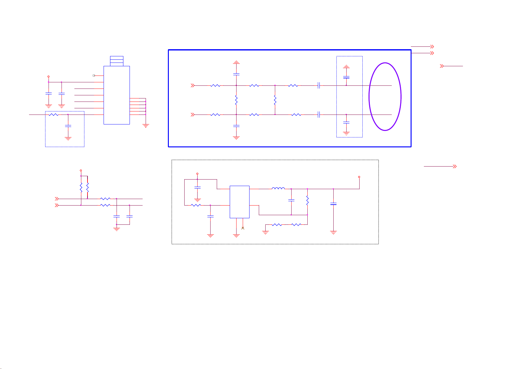
9-5-11 Tuner
TUNER3. 3V
IF_AGC T
OSDA1
OSCL1
ECN Tuner
C124
C123
100N 16V
10UF 6 .3V
R187
10K 1% 1/16W
IF_AGC _T
C119
47NF 1 6V
Closed to Tu ner
TUNER3. 3V
R178
1K2 OHM
TUN_SDA
TUN_SCL
IF_N _TU
IF_P_TU
6
6
T2 TUNER
TU101
1
ANT
2
3.3V
3
SDA
4
SCL
5
IF_N
6
IF_P
IF_AGC7TH1
ST53WS-13-E
Device Address : 0xC0
3V3: TYP: 180mA, Max: 230mA
R177
1K2 OHM
R167
R176
100R 1/1 6W 5%
100R 1/1 6W 5%
TH6
TH5
TH4
TH3
TH2
TUN_SDA
TUN_SCL
C121
56pF 50V
13
12
11
10
9
8
C122
56pF 50V
TU_FAT_IN2+
TU_FAT_IN2-
Di ff ere nt ia l P air
+5V_SW
C104
10uF 16V
R102
3K3 1/16W 5%
C106
1UF 10% 16V
C149
R122
0R05 1/16W
R123
0R05 1/16W
9
9
22N 25V
0R05 1/1 6W
R125
NC/ 620R
0R05 1/1 6W
C150
22N 25V
R120
R121
+5V_SW TO TUNER3.3V
U102 G5719TBIU
EWS_PWR
4
VIN
1
EN
GND2NC
VFB
5
3
LX
6
0R05 1/1 6W
R124
NC/ 620R
L4102 2.2uH
R8150
1K5 1%
R115
R116
0R05 1/1 6W
C103
NC/ 22P 50V
R8149
20K 1%
R8151
100K 1%
C147
1UF 10% 16V
C148
1UF 10% 16V
1000 mA
C105
10UF 1 6V
C110
33P 50V
C113
33P 50V
Closed to Tu ner
(1A/60mil)
TUNER3. 3V
IF PATH
IF_P_TU
IF_N_TU
TUNER
DVDD 3V3
+5V_SW
IF_AGC T
EWS_PWR
DVDD3V3
+5V_SW
4,5,6,7, 9,10,11,14,15, 16,17,19
5,12,19,20, 24,29
IF_AGC T
9
EWS_PWR
15
Vout=0.6 x (1+100000/22000)= 3.32 V

9-5-12 WIFI/KEYPAD
WIFI PWR CONTROL
Wi-Fi_PWR_EN :
Enable : High
Disable : Low
3V3SB
R8440
10K 5% 1/16W
RC6
R8406
100 OHM 1/16W
IR_RC
WIFI _PWR_EN
Wordmark Driver
R8413
NC/ 10K+-5%1/16W
R8415
NC/ 0R05 OHM
R8417
NC/1 0K+-5%1/16W
LED_PWM2
LED_PWM0
Add on 2016/4/22
+5V_STB
C4297
10UF 10V
R404
100R 1/16W 5%
R1197
10K 1/16W 5%
3V3SB
U714
G524D3T11U
5
IN
4
EN
R8414
NC/1 0K+-5%1/16W
R8416
NC/1 0K+-5%1/16W
Q8401
NC/L BC847BWT1G
R8412
0R05 1/16W
VOUT
2
FLG
GND
Wi-Fi_VCC
1
3
Q8400
NC/ LBC847BWT1G
R8409
0R05 1/16W
R1198
10K 1/16W 5%
R171 0 OHM 1/ 8W
R8411 N C/100OHM1/16W
R8404 100 OHM 1/16W
R8405 100 OHM 1/16W
Wi-Fi_VCC
C4265
22UF 10V
10PF 50V
C8405
C4266
100N 16V
100pF 50V
C8403
100pF 50V
3V3SB
100N 50V
C8404
M odif y by EMI 10/12
C8402
POWER_KEY
3V3SB
R5100
WoWLAN_I RQ
C8141
10P 50V
WIFI _RSTn
R4273
100R 1/16W 5%
Wi-Fi_VCC
NC/ 10K 1/16W 5%
WoWLAN_I RQn
R5103
NC/ 10K 1/16W 5%
WIFI _RESET
2017/06/27 chang to 8 pin
Wi-Fi_VCC
CN414
CONN
2
1
4
3
6
5
8
7
100R 1/ 16W 5%
3
2
C8140
10P 50V
WoWLAN_I RQn
R5115
L103
90OHM
311GW200C08ABL
TO SENSOR BOARD (CIP)
LED 1, LED2 :
Ena ble: Hi gh
Disabl e: Low
LED 2 is wordm ark
R8400
KEY_PAD0
R8403
6K8 1%
R8441
NC/ 0R05 1/16W
NC/0 R05 OHM
Updated on 2016/12/14
ZD8401
AZ5123-01H
OSCL2
R8407 10 OHM 1/16W
OSDA2
12
R8408 10 OHM 1/16W
C8401
NC/100pF 50V
C8417
10PF 50V
C8418
10PF 50V
3V3SB
R5116
NC/10K 1/16W 5%
WIF I_RSTn
R5117
4
R4267
1
R4268
NC/1 0K 1/16W 5%
Grounding(20mil)
2R2 1/16W 5%
2R2 1/16W 5%
AVDD3V3
3V3SB
+5V_SW
20
6,15
6,15
6,20
15
15
16
16
USB_DP_P2
USB_DM_P2
Updated on 2016/1/11
TP8412
TP8413
TP8414
TP8417
TP8418
TP8419
11
13
IR_RC
15
POWER_KEY
15,20
KEY_PAD0
LED_PWM0
LED_PWM2
RC6
WoWLAN_I RQ
WIFI _PWR_EN
WIFI _RESET15
USB_DP_P2
USB_DM_P2
+5V_STB
OSCL210
OSDA210
DVDD3V3
CN403
1
3
5
7
9
CONN
IR_R C
POWER_KEY
KEY_PAD0
LED_PWM0
LED_PWM2
RC6
WoWLAN_I RQ
WIFI _PWR_EN
WIFI _RESET
USB_DP_P2
USB_DM_P2
OSCL2
OSDA2
5,9,11,12, 16,19
4,5,6,9, 12,16,20
5,12,13,19, 20,24,29
4,5,9, 12,16
4,5,6, 7,9,10,11,16,17, 19
DVDD3 V3
AVDD3V3
3V3SB
+5V_SW
+5V_STB
DVDD3V3
2
4
TP8421
6
8
10
12
14

9-5-13 GPIO/ServAD
G1
G2
F3
E1
D1
D2
C2
K5
D5
E5
B3
B1
J6
D3
E4
K7
H5
D4
C4
F5
G4
G6
H6
J7
J5
K4
H4
H3
J2
A7
C7
C5
B5
B4
J4
J3
J1
B7
C6
A5
A4
A3
C1
TP5459
HSYN C
GFX-HTPDn
R8165 NC /33R 1/16W 5%
R8166 33R 1/16W 5%
YPBPR_D ETECT1
HP_DET
SYS_EEPROM_WP
I2SAMP_RESET
GFX-LOCKn
INVERTER_ON _OFF
VIDEO_D ET
PANEL_VCC_ON /OFF
USB_OCP_P0
USB_EN_P0
USB_OCP_P1
USB_EN_P1
TP5460
NC/0 R05 1/16W
R8140
33R 1/16W 5%
R8155
33R 1/16 W 5%
X_AUDIO_MON1
VSYNC
LOCKn
R8156
AJ30
AG29
AE29
AG31
AF30
AJ29
AH29
AB28
AB27
AA27
AA28
AA30
AA22
AA21
E15
D15
E16
F15
B10
E11
G15
H15
Y22
Y21
J10
F6
J15
J9
U401-8
CI_A0
CI_A1
CI_A2
CI_A3
CI_A4
CI_A5
CI_A6
CI_A7
CI_A8
CI_A9
CI_A10
CI_A11
CI_A12
CI_A13
CI_A14
CI_MCLKI
CI_MIVAL
CI_MISTRT
CI_MDI 0
CI_MDI 1
CI_MDI 2
CI_MDI 3
CI_MDI 4
CI_MDI 5
CI_MDI 6
CI_MDI 7
CI_D 0
CI_D 1
CI_D 2
CI_D 3
CI_D 4
CI_D 5
CI_D 6
CI_D 7
CI_MDO0
CI_MDO1
CI_MDO2
CI_MDO3
CI_MDO4
CI_MDO5
CI_MDO6
CI_MDO7
CI_R ST
GPIO42
GPIO43
GPIO44
GPIO45
GPIO46
GPIO48
GPIO49
GPIO50
GPIO51
GPIO52
GPIO53
GPIO54
GPIO55
GPIO56
GPIO57
GPIO58
GPIO59
GPIO60
GPIO61
GPIO62
GPIO63
GPIO64
GPIO65
GPIO66
GPIO67
GPIO68
GPIO69
GPIO70
MT5802UHOJ
GPIO0
GPIO1
GPIO2
GPIO3
GPIO4
GPIO5
GPIO6
GPIO7
GPIO8
GPIO9
GPIO10
GPIO11
GPIO12
GPIO13
GPIO14
GPIO15
GPIO16
GPIO17
GPIO18
GPIO19
GPIO20
GPIO21
GPIO22
GPIO23
GPIO24
GPIO25
GPIO26
GPIO27
GPIO28
GPIO29
GPIO30
GPIO31
GPIO32
GPIO33
GPIO34
GPIO35
GPIO36
GPIO37
GPIO38
GPIO39
GPIO40
GPIO41
GPIO47
DEMOD_RST
DEMOD_TSCLK
DEMOD_TSDATA0
DEMOD_TSDATA1
DEMOD_TSDATA2
DEMOD_TSDATA3
DEMOD_TSDATA4
DEMOD_TSDATA5
DEMOD_TSDATA6
DEMOD_TSDATA7
DEMOD_TSSYNC
DEMOD_TSVAL
CI_IN T
CI_TSCLK
CI_TSDATA0
CI_TSSYN C
CI_TSVAL
PVR_TSCLK
PVR_TSVAL
PVR_TSSYNC
PVR_TSDATA0
PVR_TSDATA1
SPI_CLK1
SPI_CLK
SPI_DATA
SPI_CLE
OPWM0
OPWM1
OPWM2
SD_D0
SD_D1
SD_D2
SD_D3
SD_CMD
SD_CLK
VCC3IO_SD
LED_PWM0
LED_PWM1
LED_PWM2
LED_PWM3
OPCTRL0
OPCTRL1
OPCTRL2
OPCTRL3
OPCTRL4
OPCTRL5
OPCTRL6
OPCTRL7
OPCTRL8
OPCTRL9
OPCTRL10
OPCTRL11
OPCTRL12
OPCTRL13
OPCTRL14
OPCTRL15
OPCTRL16
OPCTRL17
OPCTRL18
OPCTRL19
OPCTRL20
OPCTRL21
OPCTRL22
ADIN 0_SRV
ADIN 1_SRV
ADIN 2_SRV
ADIN 3_SRV
ADIN 4_SRV
ADIN 5_SRV
ADIN 6_SRV
ADIN 7_SRV
ADIN 8_SRV
ADIN 9_SRV
D11
DEMOD_RST
F10
DEMOD_TSCLK
E10
DEMOD_TSDATA0
F11
G12
F12
D12
G14
H14
J14
D10
DEMOD_TSSYNC
C11
DEMOD_TSVAL
E2
B8
G3
F4
B2
F2
A2
L7
E3
G5
K3
A8
C3
D6
AA31
AF29
AA29
H9
SD_D0
C8
SD_D1
E8
SD_D2
F8
G9
D7
SD_CLK
A10
VCC3IO_SD
L30
LED_PWM0
N28
LED_PWM1
W29
LED_PWM2
L29
J29
DEMOD_RST_STBY
K27
J30
R28
R29
M32
R8152 33R 1/16W 5%
J27
K30
G30
L31
Y32
N32
R27
T24
T25
U26
N27
G29
M25
M26
U28
R26
R25
H29
K31
H28
K28
J28
L32
F30
KEY_PAD0
N31
REG19.5V_MON
P22
AMBI_TEMP_CTL
N21
TP432
TP433
TP434
TP435
TP436
R461 0R05 1/16W
R451 33R 1/16W 5%
R452 33R 1/16W 5%
TP5457
WIF I_RESET
TUNER_WAKEU P
WoWLAN _IRQ
MHL_PWR_EN
PWRDN
BE-RESETn
WIF I_PWR_EN
SPLASH-ON
BE-PWR-EN
USB_MHL_OC
DDR _PWR_EN
EWS_PWR
POWER_KEY
BL-I-CTRBRI GHT_ADJ
SOC-AMBI-SPI-MOSI
SOC-AMBI-SPI-CLK
R415
10K 1/16W 5%
TP5458
DEMOD_RST_STBY
DVDD3V3
Close to Main Chip
VCC3IO_SD
C4200
100N 16V
DVDD3V3
TUNER_WAKEU P
R456
10K 1/16W 5%
C4201
1UF 10V
R457
10K 1/16W 5%
REG19.5V_MON
+12V
R458
NC/8 2K OHM 5% 1/16W
X_AUDIO_MON1
R459
NC/1 0K 1/16W 5%
DVDD3V 3
R460
10K 1/16W 5%
VCC&GND
3V3SB
DVDD3V 3
+5V_SW
OPCTRL
ADIN
PWM
GPIO
SDIO
GFX-HTPDn
GFX-LOCKn
I2SAMP_RESET
USB_OCP_P0
USB_EN_P0
USB_OCP_P1
USB_EN_P1
3V3SB
DVDD3V 3
+5V_SW
MHL_PWR_EN
WIF I_RESET
DDR _PWR_EN
EWS_PWR
POWER_KEY
WoWLAN _IRQ
WIF I_PWR_EN
BE-RESETn
BE-PWR-EN
SPLASH-ON
USB_MHL_OC
KEY_PAD0
AMBI_TEMP_CTL
BL-I-CTR
LED_PWM0
LED_PWM1
LED_PWM2
LOCKn
INVER TER_ON_OFF
VIDEO_D ET
PANEL_VCC _ON/OFF
PWRD N
HP_DET
SYS_EEPRO M_W P
SOC-AMBI-SPI-MOSI
SOC-AMBI-SPI-CLK
YPBPR _DETECT1
GFX-HTPDn
GFX-LOCKn
4,5,6,9, 12,14,16,20
4,5,6,7, 9,10,11,16,17,1 9
5,12,13,19, 20,24,29
MHL_PWR_EN 12
WIFI _RESET 14
DDR_PW R_EN 5
EWS_PWR
POWER_KEY
WoWLAN _IRQ
WIF I_PWR_EN
BE-RESETn
BE-PWR-EN
SPLASH-ON
USB_MHL_OC
KEY_PAD0
AMBI_TEMP_CTL
BL-I-CTR
LED_PWM0 6, 14
LED_PWM1 6
LED_PWM2
USB_OCP_P0
USB_EN_P0
USB_OCP_P1
USB_EN_P1
LOCKn
INVERTER_ON _OFF
VIDEO_DET
PANEL_VCC_ON /OFF
PWRDN
HP_DET
SYS_EEPRO M_W P
SOC-AMBI-SPI-MOSI
SOC-AMBI-SPI-CLK
YPBPR_D ETECT1
25
25
I2SAMP_RESET
13
14
14
14
24
29
24
12
14,20
20
4,24
6,14
16
16
16
16
11,25
4,24,26
9
11
10,20
19
6
24
24
9
10

9-5-14 USB/ETHERNET PHY
ETHERNET PHY
U401-10
AVDD33_ETH_STB
AVDD10_ETH_STB
MT5802UHOJ
USB_DP_P0
USB_DM_P0
USB_DP_P1
USB_DM_P1
USB_DP_P2
USB_DM_P2
SSUSB_TXP
SSUSB_TXN
SSUSB_RXP
SSUSB_RXN
AVDD33_USB
AVDD33_SSUSB_STB
AVDD33_USB_STB
AVDD10_SSUSB_STB
AVDD33_USB
C4148
10UF 6. 3V 20%
3V3SB
R477
0R05 1/16W
AVDD1V0_STB
AVDD10_ETH_STB
TXVP_0
TXVN_0
RXVP_1
RXVN_1
PHYLED 0
PHYLED 1
REXT
U401-9
B11
USB_DP_P0
A11
USB_DM_P0
B12
USB_DP_P1
A12
USB_DM_P1
T32
USB_DP_P2
T33
USB_DM_P2
V32
SSUSB_TXP
V33
SSUSB_TXN
U30
SSUSB_RXP
U31
SSUSB_RXN
L18
AVDD33_USB
M21
AVDD33_SSUSB_STB
L25
AVDD33_USB_STB
W32
AVDD10_SSUSB_STB
MT5802UHOJ
AVDD1V0_STBAVDD3V3
AVDD10_SSUSB_STB
Near IC
AVDD33_USB_STB
C4182
1uF 10V
C4202
100N 16V
P33
TXVP_0
P32
TXVN_0
R30
RXVP_1
R31
RXVN_1
V28
U27
L28
REXT
K23
AVDD33_ETH_STB
F27
AVDD10_ETH_STB
C4184
100N 16V
AVDD33_SSUSB_STB
3V3SB
R469
Near IC
100N 16V
0R05 1/16W
TXVP_0
TXVN_0
RXVP_1
RXVN_1
R445
24K 1/16W 5%
C4160
10uf 10% 10V
12
C4186
5/24 FOR EOS TEST
close to SOC
AVDD33_ETH_STB
C145
100N 16V
B1-SOD523-2L
ZD4118
U5007
1
10
CH1
NC
2
9
CH2
NC
3
8
GND
GND
4
7
CH3
NC
6
CH45NC
AZ1143-04F.R 7G
USB PORT 1
+5V_USB
500mA
USB_EN_P0
USB PORT 2 (USB 3.0)
900mA
+5V_USB
1 2
TH402
NC/PTCR
TXVP_0
TXVN_0
RXVP_1
RXVN_1
TH403
C111
1uF 10V
t
All Pa th
Groun ding(20m il)
All Pa th
Groun ding(20m il)
All Pa th
Groun ding(20m il)
t
1 2
NC/PTCR
+5V_USB
40mil
2
1
R1047
4.7K1/16W
HI = > P OWER ON
LO = > POWER O FF
USB_DP_P1
USB_DM_P1
USB_PORT1_5V
C1108
+
100UF 16V
EQUAL LENGTH and
DIFFERENTIAL
IMPEDANCE 90ohm
SSUSB_RXP
SSUSB_TXP
SSUSB_TXN
C4601
100N 16V
TXVP_0
TXVN_0
RXVP_1
RXVN_1
Must be differential 100ohm
SEPARATE GROUND
EQUAL LENGTH and
DIFFERENTIAL
OC
C1110
10uF 16V
4
5
6
H=> NORMA L
L =>OCP
R11052R2 1/16W 5%
R11062R2 1/16W 5%
IMPEDANCE 90ohm
R1025 2R2 1/ 16W 5%
R1026 2R2 1/ 16W 5%
C1015
+
100UF 16V
DVDD3V3
R1046
10K
R1049 0R05 1/16W
C1119
C1120
NC/10PF 50V
NC/10PF 50V
R1115 2R2 1/ 16W 5%
R1118 2R2 1/ 16W 5%
R1116 2R2 1/16W 5%
R1117 2R2 1/16W 5%
USB_DP_P0
USB_DM_P0
USB_PORT0_5V
U106
G529A1TB1U
IN3OUT
GND
OUT
EN
C1109
10uF 16V
C1111 100N 16V
C1112 100N 16V
C1016
NC/10PF 50V
12
ZD1102
C4602
10N 50V
C4603
100N 16V
USB_DP_P0_R
USB_DM_P0_R
C1017
NC/10PF 50V
USB_OCP_P0
12
ZD1101
AZ5413-01F.R 7GR
AZ5413-01F.R 7GR
SSUSB_RXN_RSSUSB_RXN
SSUSB_RXP_R
SSUSB_TXP_R
SSUSB_TXN_R
2
3
C4604
10N 50V
12
L805
90OHM
12
ZD107
USB_OCP_P0
1
4
RXN5RXP6GND7TXN8TXP
RJ45
CN107
1
P1
2
P2
3
P3
4
P4
5
P5
6
P6
7
P7 NC
8
P8
65
4
3
2
1234
1
ZD108
AZ5413-01F.R 7GR
AZ5413-01F.R 7GR
1D+3
4D-2
VCC
GND
USB2.0
USB3.0
9
TH1
TH2
RJ45 8P
10
CN113
R/A 6P 1*1
15,16
11
HAND110HAND2
CN112
USB CON N 9P
9
C4605
C4606
10N 50V
100N 16V
14
14
2017/6/22 relea sed(NC)
HI = > POWER ON
LO = > POWER
OFF
SSUSB_RXN_R
SSUSB_RXP_R
SSUSB_TXN_R
SSUSB_TXP_R
USB_EN_P1
BOTTOM USB
1uF 10V
R1027
4.7K1/16W
U5008
1
CH1
2
CH2
3
GND
4
CH3
CH45NC
AZ1143-04F.R 7G
GND
C1018
10
NC
9
NC
8
7
NC
6
Add USB3.0 EOS solution
OPWRSB_PWR
USB_DP_P2
USB_DM_P2
USB_PORT0_5V
+5V_USB
SSUSB_RXN_R
SSUSB_RXP_R
+5V_STB
+5V_SW
3V3SB
AVDD3V3
AVDD1V0_STB
AVDD1V0_1
DVDD3V3
USB_EN_P0
USB_EN_P1
USB_PORT1_5V
G529A1TB1U
IN3OUT
2
GND
1
EN
U108
H=> NORMA L
L =>OCP
SSUSB_TXN_R
SSUSB_TXP_R
USB_OCP_P0
USB_OCP_P1
USB_DP_P2
USB_DM_P2
1 2
OUT
OC
+5V_STB
+5V_SW
3V3SB
AVDD3V3
AVDD1V0_STB
AVDD1V0_1
DVDD3V3
USB_OCP_P0
USB_OCP_P1
OPWRSB_PWR
USB_EN_P0
USB_EN_P1
100mil
D509
FB340M
1 2
D510
FB340M
1 2
D508
FB340M
1 2
MAX=2.0A
D507
FB340M
1 2
ZD4101
NC/U DZSNP5.6B
R8130
NC/100K 1/16W
4
5
6
R1028
0R05 1/16W
R107 10K
2017/6/23 released
4,5,9,12, 14
5,12,13,19, 20,24,29
4,5,6,9, 12,14,20
5,9,11,12, 19
4,6,12
4,11,12
4,5,6,7, 9,10,11,14,15,17 ,19
15,16
15
4,5,20
15
15
+5V_STB
Q797
8
D
D
7
D
D
6
D
D
5
G4S
NC/AON 4421
C8138
NC/1U F16V
R8129
NC/33K 1/10W 5%
R8128
NC/22KOH M 1/10W
Q798
NC/MMBT3904
Option for 6.5V box
USB_PORT1_5V
USB_OCP_P1
+12V
+5V_STB
+12V
1
2
3
DVDD3V3

9-5-15 VCCK & DVSS
U401-11
Y2
AF11
AM11
AF12
AA17
AA13
AB13
AH10
AC27
AC2
AD3
AG3
AH4
AG6
AH5
AC8
W12
W15
AM8
W16
W17
W13
W33
P2
U2
AF2
AJ2
M3
AE5
R3
V3
AA3
P5
V5
B28
T6
M7
W6
AE6
AL4
E7
L6
AB7
D8
G8
T8
V8
R8
W8
AB8
AF6
AL5
T7
AE7
H8
C10
H10
AL7
M11
N11
P11
R11
T11
AK8
M12
N12
P12
R12
T12
U12
V12
P13
Y12
P15
R15
T15
U15
V15
M8
E9
P16
R16
T16
U16
V16
P17
R17
T17
U17
V17
Y17
M13
N13
R13
T13
U13
V13
N10
Y13
C13
P10
C15
M14
C12
N14
P14
AJ4
T28
U25
Y26
G27
T29
DVSS
DVSS
DVSS
DVSS
DVSS
DVSS
DVSS
DVSS
DVSS
DVSS
DVSS
DVSS
DVSS
DVSS
DVSS
DVSS
DVSS
DVSS
DVSS
DVSS
DVSS
DVSS
DVSS
DVSS
DVSS
DVSS
DVSS
DVSS
DVSS
DVSS
DVSS
DVSS
DVSS
DVSS
DVSS
DVSS
DVSS
DVSS
DVSS
DVSS
DVSS
DVSS
DVSS
DVSS
DVSS
DVSS
DVSS
DVSS
DVSS
DVSS
DVSS
DVSS
DVSS
DVSS
DVSS
DVSS
DVSS
DVSS
DVSS
DVSS
DVSS
DVSS
DVSS
DVSS
DVSS
DVSS
DVSS
DVSS
DVSS
DVSS
DVSS
DVSS
DVSS
DVSS
DVSS
DVSS
DVSS
DVSS
DVSS
DVSS
DVSS
DVSS
DVSS
DVSS
DVSS
DVSS
DVSS
DVSS
DVSS
DVSS
DVSS
DVSS
DVSS
DVSS
DVSS
DVSS
DVSS
DVSS
DVSS
DVSS
DVSS
DVSS
DVSS
DVSS
DVSS
DVSS
DVSS
DVSS
DVSS
DVSS
DVSS
DVSS
MT5802UHOJ
DVSS
DVSS
DVSS
DVSS
DVSS
DVSS
DVSS
DVSS
DVSS
DVSS
DVSS
DVSS
DVSS
DVSS
DVSS
DVSS
DVSS
DVSS
DVSS
DVSS
DVSS
DVSS
DVSS
DVSS
DVSS
DVSS
DVSS
DVSS
DVSS
DVSS
DVSS
DVSS
DVSS
DVSS
DVSS
DVSS
DVSS
DVSS
DVSS
DVSS
DVSS
DVSS
DVSS
DVSS
DVSS
DVSS
DVSS
DVSS
DVSS
DVSS
DVSS
DVSS
DVSS
DVSS
DVSS
DVSS
DVSS
DVSS
DVSS
DVSS
DVSS
DVSS
DVSS
DVSS
DVSS
DVSS
DVSS
DVSS
DVSS
DVSS
DVSS
DVSS
DVSS
DVSS
DVSS
DVSS
DVSS
DVSS
DVSS
DVSS
DVSS
DVSS
DVSS
DVSS
DVSS
DVSS
DVSS
DVSS
DVSS
DVSS
DVSS
DVSS
DVSS
DVSS
DVSS
DVSS
DVSS
DVSS
DVSS
DVSS
DVSS
DVSS
DVSS
DVSS
DVSS
DVSS
DVSS
DVSS
DVSS
DVSS
DVSS
DVSS
H16
J16
C24
D24
E24
F24
L16
AC16
F29
M17
C18
T30
A32
C20
C22
D22
H25
AJ25
G26
H26
E25
AL10
AJ26
AJ12
AL13
AM14
P21
AJ28
AE31
T31
W22
V22
U22
V31
F9
AG20
AC31
N20
AL19
AH32
N33
W21
V21
U21
T21
R21
AF19
N19
AA20
Y20
W20
V20
U20
T20
R20
P20
P18
N18
N17
C17
AA19
Y19
W19
V19
U19
T19
R19
P19
AF16
AE16
AA16
Y16
N16
AA18
Y18
W18
V18
U18
T18
R18
M16
AF15
AB15
AA15
Y15
N15
M15
AL16
AB14
AA14
Y14
W14
V14
U14
T14
R14
AL22
R10
K15
AC13
AC12
AM20
AM17
T22
L5
F20
V29
K6
F7
J8
G10
AD27
VCCK
AC19
AD21
AC20
AD20
AC21
AC17
AC22
AC18
W23
AA23
AB23
AC23
AD23
W24
AA24
AB24
AC24
AD24
AB25
AC25
AD25
AE25
AF25
AD26
AE26
AF26
AG26
AF24
AA25
AG25
AF27
AG27
AE21
AE24
W25
AH26
AB17
AB18
Y23
Y24
V23
V24
V25
Y25
U401-12
VCCK
VCCK
VCCK
VCCK
VCCK
VCCK
VCCK
VCCK
VCCK
VCCK
VCCK
VCCK
VCCK
VCCK
VCCK
VCCK
VCCK
VCCK
VCCK
VCCK
VCCK
VCCK
VCCK
VCCK
VCCK
VCCK
VCCK
VCCK
VCCK
VCCK
VCCK
VCCK
VCCK
VCCK
VCCK
VCCK
VCCK
VCCK
VCCK
VCCK
VCCK
VCCK
VCCK
VCCK
MT5802UHOJ
Capacitor s close to IC
VCCK
C4141
C4175
22UF
22UF
VCC3IO_A
VCC3IO_B
NC
NC
NC
NC
L2
AH33
AN33
A33
AN1
A1
C4166
NC/10uF 6.3V
VCC3IO_A
VCC3IO_B
VCC3IO_AB
C4152
4.7UF 6.3V
C4158
100N 16V
DVDD3V34,5,6,7,9, 10,11,14,15,16,19
VCCK5,6,7
C4161
100N 16V
VCCK
VCC3IO_AB
C4162
100N 16V
C4144
100N 16V
VCCK
C4145
1uF 10V
C4165
1uF 10V
C4147
100N 16V
C4193
1uF 10V

9-5-16 DDR POWER
R475
47R 1/16W 5%
DDRV
DDR V
U401-13
AG8
AA9
AF9
U10
K2
L9
L4
N9
Y9
T10
P9
DDR VREF_C1
CRTN
ZQ_C1
DDR V
DDR V
DDR V
DDR V
DDR V
DDR V
DDR V
DDR V_CKC
MT5802UHOJ
DDRV
DDRV
DDRV
DDRV
DDRV
DDRV
DDRV
V10
W10
Y10
AA10
AB10
AC10
AC11
DDR V
R441
1K 1/16W 1%
DDR VREF_C1
R442
1K 1/16W 1%
DDR VREF_C1
CRTN
ZQ_C1
DDR V
R440
240R 1%
DRAM Power
Bottom Side Capacitors close to IC
C4128
100N 16V
C4127
100N 16V
DDRV
C4099
100N 16V
DDR V
C4129
1UF 6.3V
Cap close to DDRV power source.
C4130
100N 16V
+
C4139
NC/ 47uF 16V
C4194
1UF 6.3V
C4167
10uF 6. 3V
C4131
100N 16V
C4098
4.7UF 10% 10V
C4132
100N 16V
C4095
10uF 6. 3V
C4133
100N 16V
C4134
100N 16V
C4135
100N 16V
C4136
100N 16V
C4092
100N 16V
C4124
NC/1 0uF 6.3V
C4091
100N 16V
C4115
100N 16V
C4093
100N 16V
C4094
100N 16V
C4168
1UF 6. 3V
C4169
100N 16V
C4170
100N 16V
C4171
100N 16V
C4172
100N 16V

9-5-17 LINE OUT/SPDIF
AIN_R 0
AIN_L0
TP103
TP104
AVDD33_AADC
VMID_AADC
C4153
100N 16V
HEADPHONE
AR0O
All Pa th
Grounding(20mil)
U401-4
D26
AIN_R0
A26
AIN_L0
C26
AIN_R1
B27
AIN_L1
C4154
1uF 10V
B26
AIN_R2
C27
AIN_L2
K21
AVDD33_AADC
D29
VMID_AADC
K22
AVSS33_CLN
MT5802UHOJ
C682
+
100UF 16V
for PCB
space
C683
+
100UF 16V
AIN_R 2 AR1O
AIN_L2
AVSS33_CLN
AL0_ADAC
AR0_ADAC
AL1_ADAC
AR1_ADAC
AVDD33_ADAC
ASPDIF O0
ASPDIF O1
AOSDATA4
AOSDATA3
AOSDATA2
AOSDATA1
AOSDATA0
OUTR HPOUTR
OUTL
R675
R676
22K 1/16W 5%
ASPDIF I
AOBCK
AOLRCK
AOMCLK
10R 1/ 10W 5%
10R 1/ 10W 5%
22K 1/16W 5%
A28
AL0O
C28
AR0O
C29
AL1O
D28
J21
AVDD33_ADAC
AG30
HTPDn
Y33
ASPDIF O0
F17
ASPDIF O1
AK32
AOBCK
AJ31
AOLRCK
AL33
R101 22R 1/16W 5%
AH30
AJ33
AJ32
AH31
AOSDATA1
AK33
AOSDATA0
R653
C660
NC/ 6.8NF 50V
R654
C661
NC/ 6.8NF 50V
HP Audi o o ut
with GND
HPOUTLAL0O
TP5461
TP5462
R655 0R05 1/16W
TP101
AOMCLK
C4204
10PF 50V
HP_DET
Low: normal
High: HP detect
HP_DET
HPOUTR
HPOUTL
wi th GND
AVDD3V3
R646
R647
AVDD33_ADAC
ARC
C1033
33P 50V
0R05 1/10W
0R05 1/10W
Analog Power
AVDD33_AADC
C4150
100N 16V
R656
33R 1/16W 5%
R619
0R05 1/ 16W
12
C654
C653
NC/ 100N 16V
ZD131
NC/ 100N 16V
TVM1G5R5M 100R
DVDD3V3
12
ZD132
TVM1G5R5M 100R
C4157
10uF 6.3 V
SPDIF _OUT
C1043
47PF 50V
R641
4K7 1/16W 5%
R618 0R05 1/ 16W
C662
NC/ 470pF 50V
Spdif Out
with GND
3
4
2
5
1
12
CN602
PHONE JACK 5P
ZD129
TVM1G5R5M 100R
+5V_SW
C1026
100N 16V
ARC
AOMCLK
AOBCK
AOLRCK
AOSDATA0
HP_DET
AIN_R 0
AIN_L0
+5V_SW
AVDD3V3
DVDD3V3
1
2
3
CN104
OPTICAL
VIN
VCC
GND
TH14TH25TH36TH4
HP_DET
+5V_SW
AVDD3V3
DVDD3V3
7
ARC
AOMCLK
AOBCK
AOLRCK
AOSDATA0
AIN_R 0
AIN_L0
12
10
10
10
10
15
9
9
5,12,13,20, 24,29
5,9,11, 12,16
4,5,6,7 ,9,10,11,14,15,1 6,17
HTPDn
HTPDn
11,25
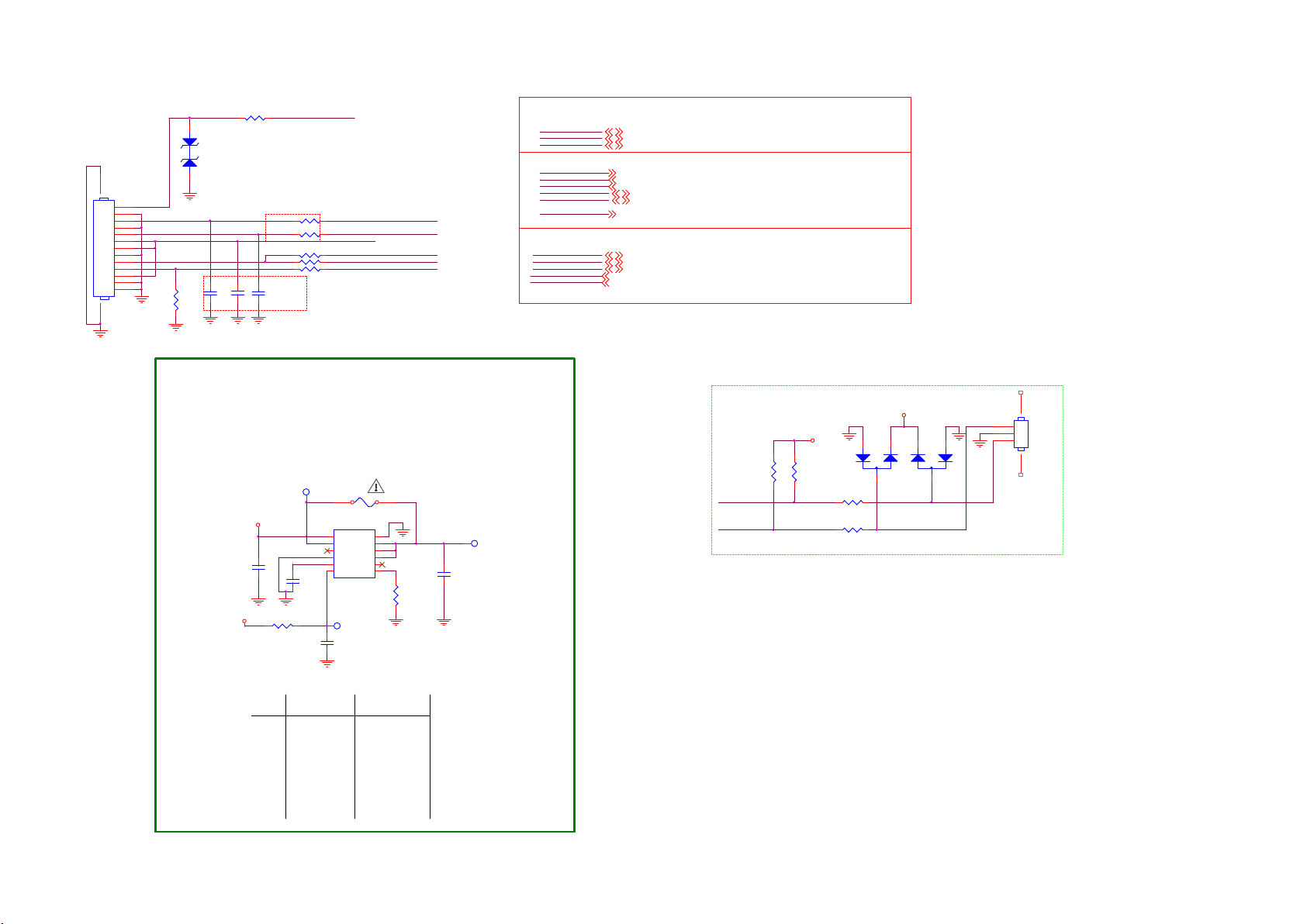
9-5-18 AMBILIGHT & HTV CNN
12
ZD127
AL+KEY
1415
CN412
COMM
1
2
3
4
5
6
7
8
9
10
11
12
13
Key1
+12V_AMBI
R8144
0R05 1/16W
AZ5123-01H.R 7G
C402
100P 50V
Mo dify by EM I 10/12
AMBILIGHT PROTECTION
R4501
100R 1/16W 1%
R8131 47R 1/16W 5%
R8132 47R 1/16W 5%
R4502 0R 05 1/16W
R8145 N C 0R05 1/16W
R8146 N C 0R05 1/16W
C8139
C404
100P 50V
100N 50V
KEY_PAD0
+12V_AMBI
AMBI-SPI-CLK
AMBI-SPI-MOSI
AMBI_TEMP_CTL
SCL-AMBI
SDA-AMBI
VCC&GND
3V3SB
+5V_SW
DVDD3V3
Ambi-light
AMBI_TEMP_CTL
AMBI-SPI-MOSI
AMBI-SPI-CLK
SCL-AMBI
SDA-AMBI
KEY_PAD0
BUH Speaker
IR_RC
U0TX
U0RX
OPWRSB_PWR
PWRDN
3V3SB
+5V_SW
DVDD3V3
AMBI_TEMP_CTL
AMBI-SPI-MOSI
AMBI-SPI-CLK
SCL-AMBI
SDA-AMBI
KEY_PAD0
IR_RC
U0TX
U0RX
OPWRSB_PWR
PWRDN
4,5,6,9, 12,14,16
5,12,13,19, 24,29
4,5,6,7, 9,10,11,14,15,16, 17,19
15
24
24
24
24
14,15
14
6
6
4,5
10,15
+12V
C4457
1uF 25V
DVDD3V3
R4430
10K 5% 1/16W
F4400
C4457
C4459
C4458
R4430
C4456
U4405
C4454
R4428
TP4441
2 Sided ambilight 3|4 Sided ambilight
U4404
F4400
1 2
NC/T 2A 63V
U4405
1
2
3
4
5
C4454
47NF 16V
TP4442
X
X
X
X
NA
NA
NA
NA
NA
IN
GND
IN
OUT
NC
OUT
GND
OUT
SS
EN6SET
AOZ1360DIL
C4456
100NF 16V
12
11
10
9
8
NC
7
1uF 25V
R4428
47K 1/16W
NA
X
X
X
X
X
X
X
X
C4458
+12V_AMBI
TP4440
UART Port 0
3V3SB
R8137
R8138
4.7K1/16W
U0RX
U0TX
FOR CODE DOWNLOAD AND DEBUG
4.7K1/16W
R8136
R8135
1
2
3
100R 1/16W 5%
100R 1/16W 5%
3V3SB
D4002
BAV99
45
CN406
1
CONN
2
1
2
D4003
BAV99
3
3
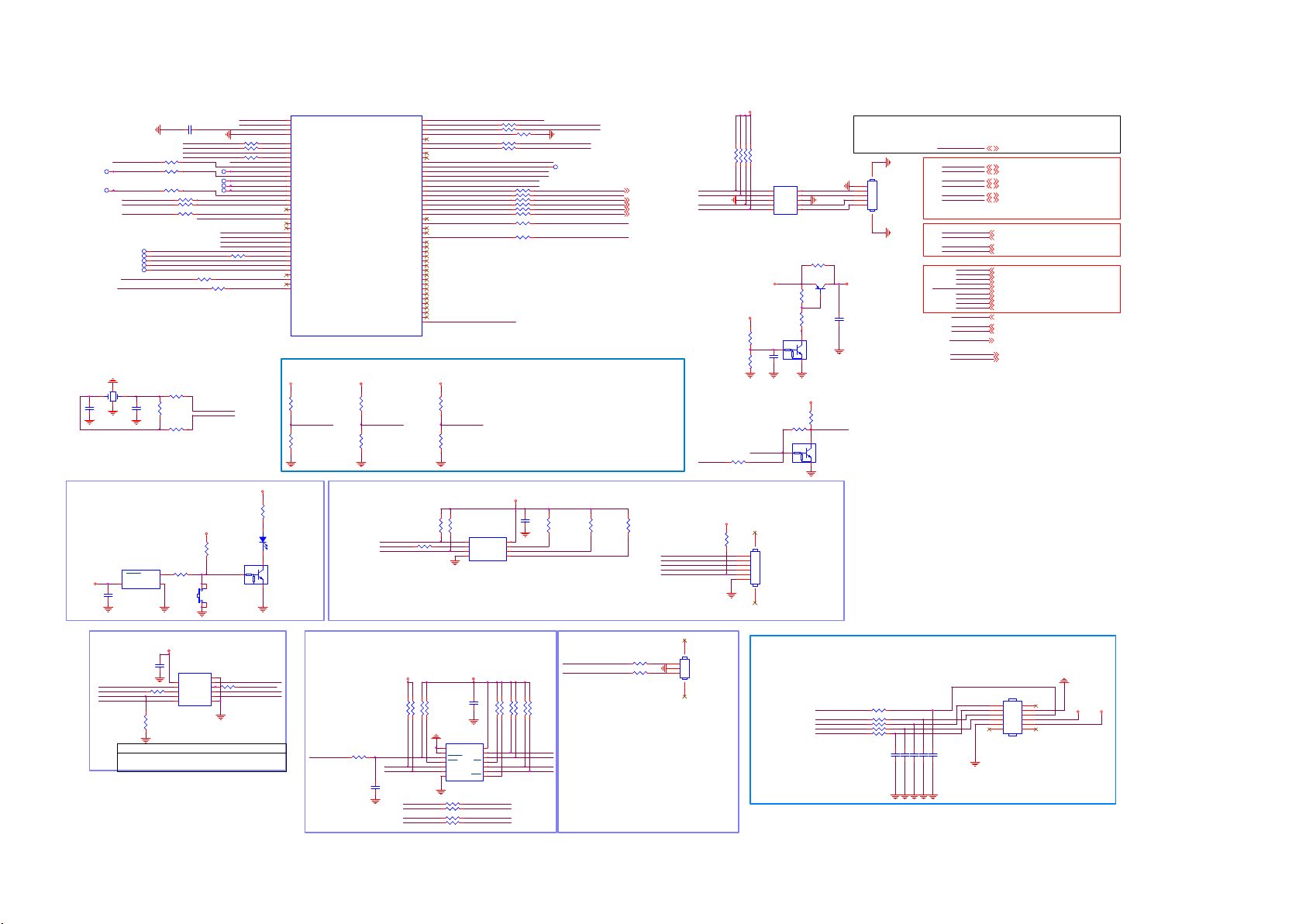
9-5-19 NT334a_CONTROL
NT334 CONTROL
NT-SPI-CS BS2
NT-SPI-CLK BS1
NT-SPI-DI
R3102 NC/ 0R05 OHM
R3112 NC/ 0R05 OHM
R3122 NC/ 0R05 OHMTP4385
R5193 N C/33R 1/1 6W 5%
R5188 33R 1/16W 5%
R5189 33R 1/16W 5%
M_SPI1_CSN
M_SPI1_CLK
M_SPI1_DI
M_SPI1_DO
3D_LR_IN_OSD
RA3175
100 OHM 1/16W
RA3178
CA3107
10PF 50V
1M 1/16W
RA3186
100 OHM 1/16W
4.7K 1/16W
RA3154
2
1
GND
NT-SPI-DO BS0
RA4949 33R 1/16W 5%
RA3145
BL-DIM2
BL-DIM4
TP4380 TP4381
BL-DIM8
NT-AMBI-SPI-CLK
NT-AMBI-SPI-MOSI LED_ SPI1_DO
TP4374
TP4375
TP4376
TP4377
TP4378
NT-CTRL-DISP5_NT-3D-LR
LDM-SPI-VSYNC
X3100
1243
12MHZ
CA3106
10PF 50V
RESET
U3101
RT9818C-29GVL
RESET(RESET)
3
+3V3-NT
VDD
CA3102
100NF 16V
CA3108100NF 16V
TP4382
TP4383
TP4384
BL-I-CTRLn
NT-DSU-TX
NT-DSU-RX
NT-UART-TX
NT-UART-RX
R7601 33R 1/16W 5%
R3137 N C/22 OHM 1/16W
XTAL_OUT
XTAL_IN
+3V3-NT
GPTS06033GC1-PB
BE-RESETn
0R05 OHM
SW3100
BE-RESETn
Add text
XTAL_OUT
XTAL_IN
BE-RESETn
R7604 47 OHM 1/16W
R7600 33R 1/1 6W 5%
R7605 47 OHM 1/16W
BL-DIM1n
BL-DIM3
BL-DIM5
BL-DIM6
BL-DIM7
LED_SPI1_CSNT-AMBI-SPI-SWITCH
LED_SPI1_CK
+3V3-NT
LED3102
R1
1
R2
U5000D
T31
XI
T30
XO
P28
SYS-RST
AJ2
TESTM
AL1
GPIOA00/M_SPI0_CS/BS2
AJ1
GPIOA01/M_SPI0_CK/BS1
AL2
GPIOA02/M_SPI0_DI
AK2
GPIOA03/M_SPI0_DO/BS0
W27
GPIOA04/VPWM0/LED_SPI0_CS0
W28
GPIOA05/VPWM1/LED_SPI0_SCK
Y28
GPIOA06/VPWM2/LED_SPI0_SDI
V32
GPIOA07/VPWM3/LED_SPI0_SDO
V31
GPIOA08/VPWM4/LED_SPI0_CS1
V30
GPIOA09/VPWM5/LED_SPI0_CS2
W30
GPIOA10/VPWM6/LED_SPI0_CS3
Y30
GPIOA11/VPWM7/LED_SPI0_STT
AD26
GPIOA12/LED_SPI1_CS
AA26
GPIOA13/LED_SPI1_CK
AB28
GPIOA14/LED_SPI1_DI
AB27
GPIOA15/LED_SPI1_DO
Y32
GPIOA16/PWM_OUT-1
AA32
GPIOA17/PWM_IN-1
Y31
GPIOA18/PWM_IN-2
N26
GPIOA19/DSU-TX
M26
GPIOA20/DSU-RX
N28
GPIOA21/UART-TX
N27
GPIOA22/UART-RX
U27
GPIOA23/M_SPI1_CS
U26
GPIOA24/M_SPI1_CK
V26
GPIOA25/M_SPI1_DI
W26
GPIOA26/M_SPI1_DO
AC30
GPIOA27/3D_LR_IN_ OSD
AC31
GPIOA28/3D_LR_IN
AC32
GPIOA29/3D_IR_OUT_0_M
Y27
GPIOA30/3D_IR_OUT_1_M
Y26
GPIOA31/3D_IR_OUT_2_M
VNT72334TBG
FRC_3.3V
RA3142
470 OHM 1/16W
12
Add text
BE-RESETn
32
Q3104
LMUN5211T1G
R5191
10K 5% 1/16W
SI2C_ADDR _SEL
R5190
NC/10K 5% 1 /16W
GPIOB01/MI2C_SCL
GPIOB02/MI2C_SDA
GPIOB05/SI2C_SCL
GPIOB06/SI2C_SDA
GPIOB08/MSPI1_WP
GPIOB09/MSPI0_WP
GPIOB13/M_SPI0_IF_HI Z
GPIOB14/I2C_THROU GH
GPIOB15/LOCK/CR D/SFC
GPIOB16/CTG_1
GPIOB17/CTG_2
GPIOB18/CTG_3
GPIOB19/CTG_4
GPIOB20/CTG_5
GPIOB21/CTG_6
GPIOB22/CTG_7
GPIOB23/CTG_8
GPIOB24/CTG_9
GPIOB25/CTG_10
GPIOB26/CTG_11
GPIOB27/CTG_12
GPIOB28/CTG_13
GPIOB29/CTG_14
GPIOB30//CTG_15
GPIOB31/CTG_16
GPIOC06/CTG_17
GPIOC07/CTG_18
GPIOC08/CTG_19
GPIOC09/CTG_20
GPIOC10/CTG_21
GPIOC11/CTG_22
GPIOC12/CTG_23
GPIOC13/CTG_24
GPIOC14/CTG_25
GPIOC15/CTG_26
GPIOC16/CTG_27
GPIOC17/SI2C_AD DR_SEL
FRC_3.3V
R5192
NC/10K 5% 1 /16W
I2C_THROUGH
R5194
10K
NT-SPI-CS BS2
NT-SPI-DI
NT-SPI-WP
AB30
GPIOB00
T27
T28
AC28
GPIOB03/BS3
AC27
GPIOB04
AA31
AA30
R26
GPIOB07
U28
AK1
T26
GPIOB10
AC26
GPIOB11
AB26
GPIOB12
AH26
AG26
E28
E27
E26
F26
G26
G27
G28
H28
H27
H26
J26
K26
K27
K28
L28
L27
L26
H15
H14
F13
H13
H11
J13
G12
J12
H12
G13
J14
AM2
FLASH
RA3146
10K 5% 1/16W
RA3151 47 OHM 1/16W
GPIOB_03
GPIOB_05
GPIOB_06
GPIOB_09 M_SPI0_WPN NT-SPI-WP
GPIOB_13 N T-FLASH-HIZn
GPIOB_14 I 2C_THROUGH
GPIOB_15
GPIOB_16
GPIOB_17
GPIOB_18
GPIOB_19
GPIOB_20
GPIOB_22
GPIOB_25
GPIOC_17 SI2C_ADDR_SEL
FLASH_HIZN: Dedicated GPIO which make SPI FLASH IF Hi-Z
H: GPIOA [3..0] and GPIOA[26..23] Normal mode (Default)
FRC_3.3V
L: GPIOA [3..0] and GPIOA[26..23] HI-Z for SPI FLASH burn code by External
Flash Writer (For Factory update Flash application)
R5196
10K
NT-FLASH-HIZ n
R5195
NC/10K 5% 1 /16W
RA3147
10K 5% 1/16W
1
2
3
R7606 47 OHM 1/16 W
R7607 47 OHM 1/16 W
NT-CTRL-DISP9
NT-CTRL-DISP7
NT-CTRL-DISP8
Wide
U3102
CS#
VCC
SO/SIO1
HOLD#
WP#
SCLK
GND4SI/SIO0
MX25L3206EM2I-12G
R5061
10K 1/16W
RA504833R 1/16W 5%
RA504933R 1/16W 5%
RA505033R 1/16W 5%
RA505133R 1/16W 5%
RA505233R 1/16W 5%
RA504733R 1/16W 5%
RA505333R 1/16W 5%
R5056 33R 1/16W 5%
+3V3-NT
8
7
6
5
NT-CTRL-DISP3
R7608 NC/ 47 OHM 1/16W
R7609 NC/ 47 OHM 1/16W
SCL-DISP
SDA-DISP
STB_SCL
STB_SDA
TP3113
INVERTER_ON_OFF
SPLASH-ON
NT-CTRL-DISP1
NT-CTRL-DISP2
NT-CTRL-DISP4
NT-CTRL-DISP6
I2C_THROUGH: Dedicated GPIO which make I2C Loopth
(GPIOB_5,6 Loopth to GPIOB_1,2: SoC I2C signal will Loopth
to Panel side)
H: I2C Loop through mode.
L: Normal mode. (Default)
SI2C ADDR(PD)
H: Address 0x34H(Default)
L: Address 0x30H
CA3100
RA3148
100NF 16V
10K 5% 1/16W
NT-SPI-HOLD
NT-SPI-CLK BS1
NT-SPI-DO BS0
NT-AMBI-SPI-SWITCH
NT-LCD-PWR-ON
RA3155
10K 5% 1/16W
NVT CONTROL BL
INVERTER_ON_OFF
NT-CTRL-DISP1
NT-CTRL-DISP2
NT-CTRL-DISP4
NT-CTRL-DISP6
RA3156
10K 5% 1/16W
4,15,24,26
24,26
24,26
24,26
24,26
NT-SPI-CLK
NT-SPI-CS
NT-SPI-DO
NT-SPI-DI
NT-FLASH-HIZ n
NT-DSU-RX
NT-DSU-TX
NT-UART-RX
NT-UART-TX
BL-I-CTRLn
RA3116 4.7K 1/16W
Panel_12V
RA3152
22K 1/16W
RA3153
22K 1/16W
RA7630
NC/0R05 OHM
+3V3-NT
1K 1/16W
RA3149
RA3113 4.7K 1/16W
+3V3-NT
Layout:
Place together
RA3117 4.7K 1/16W
RA3114 4.7K 1/16W
U5009
1
CH1
2
CH2
3
GND
GND
4
CH3
CH45NC
AZ1143-04F.R7G
+3V3-NT
10K 5% 1/16W
4.7K 1/16W
Q3105
LMUN5211T1G
R1
1
R2
CA3103
1uF 10V
0R05 OHM
BL-DIM1n
Progra mm ing
78
CN1042
1
2
3
Add text
4
NT-SPI-FLASH
5
6
NC
NC
NC
RA3144
RA3150
RA3101
1
R1
R2
10
9
8
7
6
0R05 OHM
BTA1576S3
32
+3V3-DISP
NT-DSU-RX
NT-DSU-TX
NT-UART-RX
NT-UART-TX
RA3143
Q3103
2 3
1
RA3100
1K 1/16W
32
Q3100
NC/LMUN5211T1G
CA3101100nF 16V
BL-I-CTR
+3V3-DISP
VCC&GND
67
1
2
3
4
5
CN1014
CONN
+5V_SW
IIC bus
SCL-AMBI
SDA-AMBI
SCL-DISP
SDA-DISP
STB_SCL
STB_SDA
SPI bus
AMBI-SPI-MOSI
AMBI-SPI-CLK
SOC-AMBI-SPI-MOSI
SOC-AMBI-SPI-CLK
NovaTek CTRL-DISP
NT-CTRL-DISP1
NT-CTRL-DISP2
NT-CTRL-DISP3
NT-CTRL-DISP4
NT-CTRL-DISP5_NT-3D-LR
NT-CTRL-DISP6
NT-CTRL-DISP8
NT-CTRL-DISP7
NT-CTRL-DISP9
Others
NT-LCD-PWR-ON
SPLASH-ON
BE-RESETn
INVERTER_ON_OFF
BL-I-CTR
BL-DIM1n
+5V_SW
SCL-AMBI
SDA-AMBI
SCL-DISP
SDA-DISP
STB_SCL
STB_SDA
20
AMBI-SPI-MOSI
20
AMBI-SPI-CLK
15
SOC-AMBI-SPI-MOSI
15
SOC-AMBI-SPI-CLK
24,26
NT-CTRL-DISP1
24,26
NT-CTRL-DISP2
26
NT-CTRL-DISP3
24,26
NT-CTRL-DISP4
NT-CTRL-DISP5_NT-3D-LR
24,26
NT-CTRL-DISP6
26
NT-CTRL-DISP8
26
NT-CTRL-DISP7
26
NT-CTRL-DISP9
4,11
NT-LCD-PWR-ON
15
SPLASH-ON
15
BE-RESETn
4,15,24,26
INVERTER_ON_OFF
BL-I-CTR
BL-DIM1n
5,12,13,19,20,29
20
20
26
26
6
6
26
4,15
26
AM BI SPI SWITCH
NT-AMBI-SPI-CLK
AMBI-SPI-CLK
NT-AMBI-SPI-SWITCH
SOC-AMBI-SPI-CLK
+3V3
CA3121
100nF 16V
RA3231
22 OHM 1/16W
RA3238
4.7K 1/16W
MT5802 Control
SOC-AMBI-SPI-MOSI
SOC-AMBI-SPI-CLK
NX3L4684TK
U3604
E-PAD
1
VCC
2Y1
2
1Y1
2Z
3
1Z
2S
4
1S
2Y0
1Y05GND
NT72334 Control
NT-AMBI-SPI-MOSI
NT-AMBI-SPI-CLK
11
10
9
8
7
6
NT-AMBI-SPI-MOSI
AMBI-SPI-MOSI
NT-AMBI-SPI-SWITCH
SOC-AMBI-SPI-MOSI
RA3230
22 OHM 1/16W
Switch ouput
AMBI-SPI-MOSI
AMBI-SPI-CLK
BE-I2C-MUX
BE-RESETn
RA3183 100 OHM 1/16W
CA3109
100nF 16V
Updated on 2015/10/17
+3V3-DISP
SDA-DISP
SCL-DISP
RA31614.7K 1/16W
STB_SDA
STB_SCL
STB_SDA
STB_SCL
RA31624.7K 1/16W
RA316410K 5% 1/16W
RA316310K 5% 1/16W
100nF 16V
U3104
1
A0
2
A1
3
RESET
4
INT0
5
SD0
6
SC0
GND7INT1
PCA9543APWR
RA3191 NC/0R05 OHM
RA3192 NC/0R05 OHM
RA3193 NC/0R05 OHM
RA3194 NC/0R05 OHM
CA3105
+3V3-NT
VCC
DEBUG
STB_SCL
STB_SDA
RA316610K 5% 1/16W
RA31692. 2K 1/16W
RA31742. 2K 1/16W
RA316710K 5% 1/16W
RA31702. 2K 1/16W
RA31762. 2K 1/16W
14
13
SDA
12
SCL
11
INT
10
SC1
9
SD1
8
STB_SDA
STB_SCL
SCL-AMBI
SDA-AMBI
45
CN1023
1
RA319747 OHM 1/16W
2
CONN 3P
3
RA319847 OHM 1/16W
Add text
I2C-BE
LDM-SPI-CLK
LDM-SPI-MOSI
LDM-SPI-VSYNC
LDM-SPI-MISO
LDM-SPI-CS
BL-DIM2
BL-DIM4
LDM-SPI-VSYNC
BL-DIM3
BL-DIM8
2Ddim ming
R3225 N C/10 OHM 1/ 16W
R3242 N C/10 OHM 1/ 16W
R3243 N C/10 OHM 1/ 16W
R3244 N C/10 OHM 1/ 16W
R3245 N C/10 OHM 1/ 16W
C3224NC/ 10PF 50V
CN1163
2
1
4
3
6
5
8
7
10
9
12
11
C3220NC/ 10PF 50V
C3221NC/ 10PF 50V
C3222NC/ 10PF 50V
C3223NC/ 10PF 50V
NC/CON N
+5V_SW
+12V
Updated on 2017/6/28
SDA-DISP
SCL-DISP
SDA-AMBI
SCL-AMBI

9-5-20 NT334b_RX_VB1
NT334 Vx1 INPUT
Add on 2015/10/23
SOC-VB1-TX0p
SOC-VB1-TX0n
SOC-VB1-TX1p
SOC-VB1-TX1n
SOC-VB1-TX2p
SOC-VB1-TX2n
SOC-VB1-TX3p
SOC-VB1-TX3n
SOC-VB1-TX4p
SOC-VB1-TX4n
SOC-VB1-TX5p
SOC-VB1-TX5n
SOC-VB1-TX6p
SOC-VB1-TX6n
SOC-VB1-TX7p
SOC-VB1-TX7n
HTPDn
LOCKn
GFX-HTPDn
GFX-LOCKn
LOCKn
12K 1% 1/16W
TP4433
TP4434
RA7603 0R05 OHM
RA7602 0R05 OHM
+3V3
RA334110K 5% 1/ 16W
RA334210K 5% 1/ 16W
RA333710K 5% 1/ 16W
RA333910K 5% 1/ 16W
RA7613100R 1/ 16W 1%
RA7614100R 1/ 16W 1%
RA7615100R 1/ 16W 1%
RA7616100R 1/ 16W 1%
RA7617100R 1/ 16W 1%
RA7618100R 1/ 16W 1%
RA7619100R 1/ 16W 1%
RA7620100R 1/ 16W 1%
RA7621100R 1/ 16W 1%
RA7622100R 1/ 16W 1%
RA7623100R 1/ 16W 1%
RA7624100R 1/ 16W 1%
RA7625100R 1/ 16W 1%
RA7626100R 1/ 16W 1%
RA7627100R 1/ 16W 1%
RA7628100R 1/ 16W 1%
RA5185
VRX_HTPD_BN
VRX_LOCK_BN
NT-VRX0p
NT-VRX0n
NT-VRX1p
NT-VRX1n
NT-VRX2p
NT-VRX2n
NT-VRX3p
NT-VRX3n
NT-VRX4p
NT-VRX4n
NT-VRX5p
NT-VRX5n
NT-VRX6p
NT-VRX6n
NT-VRX7p
NT-VRX7n
GFX-VB1-TX0p
GFX-VB1-TX0n
GFX-VB1-TX1p
GFX-VB1-TX1n
GFX-VB1-TX2p
GFX-VB1-TX2n
GFX-VB1-TX3p
GFX-VB1-TX3n
RA5184100R 1/ 16W 1%
RA5186100R 1/ 16W 1%
RA5182100R 1/ 16W 1%
RA5183100R 1/ 16W 1%
RA7595100R 1/ 16W 1%
RA7596100R 1/ 16W 1%
VRX_HTPD_BNHTPDn
VRX_LOCK_BN
AL26
AM26
AK27
AK26
AL28
AK28
AM29
AM28
AK29
AL29
AK31
AK30
AM31
AL31
AK32
AL32
AJ31
AJ32
AH30
AJ30
AG31
AG30
AF32
AG32
AE30
AF26
AH28
AG28
AF28
AD31
AD32
U5000B
VRX0P
VRX0N
VRX1P
VRX1N
VRX2P
VRX2N
VRX3P
VRX3N
VRX4P
VRX4N
VRX5P
VRX5N
VRX6P
VRX6N
VRX7P
VRX7N
VRX8P
VRX8N
VRX9P
VRX9N
VRX10P
VRX10N
VRX11P
VRX11N
VRXREXT
VRXHTP_A
VRXLOCK_A
VRXHTP_B
VRXLOCK_B
VRXHTP_C
VRXLOCK_C
VNT72334TBG
GFX-LOCKn
LOCKn
RA3215 N C/1K 1/16W
GPTS06033GC1-PB
LED3205
RA3217 NC/1K 1/16W
1
1
+3V3-NT
LED3203
GPTS06033GC1-PB
12
Add text
GFX-LOCKn
23
Q3200
LBC857BWT1G
RA3216
470 OHM 1/16W
+3V3-NT
12
Add text
PQ-LOCKn
23
Q3201
LBC857BWT1G
RA3218
470 OHM 1/16W
GFX-HTPDn
GFX-LOCKn
GFX-VB1-TX0n
GFX-VB1-TX0p
GFX-VB1-TX1n
GFX-VB1-TX1p
GFX-VB1-TX2n
GFX-VB1-TX2p
GFX-VB1-TX3n
GFX-VB1-TX3p
SOC-VB1-TX0n
SOC-VB1-TX0p
SOC-VB1-TX1n
SOC-VB1-TX1p
SOC-VB1-TX2n
SOC-VB1-TX2p
SOC-VB1-TX3n
SOC-VB1-TX3p
SOC-VB1-TX4n
SOC-VB1-TX4p
SOC-VB1-TX5n
SOC-VB1-TX5p
SOC-VB1-TX6n
SOC-VB1-TX6p
SOC-VB1-TX7n
SOC-VB1-TX7p
HTPDn
LOCKn
GFX-HTPDn
GFX-LOCKn
GFX-VB1-TX0n
GFX-VB1-TX0p
GFX-VB1-TX1n
GFX-VB1-TX1p
GFX-VB1-TX2n
GFX-VB1-TX2p
GFX-VB1-TX3n
GFX-VB1-TX3p
SOC-VB1-TX0n
SOC-VB1-TX0p
SOC-VB1-TX1n
SOC-VB1-TX1p
SOC-VB1-TX2n
SOC-VB1-TX2p
SOC-VB1-TX3n
SOC-VB1-TX3p
SOC-VB1-TX4n
SOC-VB1-TX4p
SOC-VB1-TX5n
SOC-VB1-TX5p
SOC-VB1-TX6n
SOC-VB1-TX6p
SOC-VB1-TX7n
SOC-VB1-TX7p
HTPDn
LOCKn
15
15
11
11
11
11
11
11
11
11
11
11
11
11
11
11
11
11
11
11
11
11
11
11
11
11
11,19
11,15
GFX-HTPDn
GFX-LOCKn
HTPDn
LOCKn

9-5-21 NT334c_TX_VB1
NT334 V-BY-1 OUTPUT
U5000C
MTXA0P
MTXA0N
MTXA1P
MTXA1N
MTXA2P
MTXA2N
MTXACKP
MTXACKN
MTXA3P
MTXA3N
MTXA4P
MTXA4N
MTXA5P
MTXA5N
MTXB0P
MTXB0N
MTXB1P
MTXB1N
MTXB2P
MTXB2N
MTXBCKP
MTXBCKN
MTXB3P
MTXB3N
MTXB4P
MTXB4N
MTXB5P
MTXB5N
MTXC0P
MTXC0N
MTXC1P
MTXC1N
MTXC2P
MTXC2N
MTXCCKP
MTXCCKN
MTXC3P
MTXC3N
MTXC4P
MTXC4N
MTXC5P
MTXC5N
MTXD0P
MTXD0N
MTXD1P
MTXD1N
MTXD2P
MTXD2N
MTXDCKP
MTXDCKN
MTXD3P
MTXD3N
MTXD4P
MTXD4N
MTXD5P
MTXD5N
VNT72334TBG
MTXE0P
MTXE0N
MTXE1P_VTX0P
MTXE1N_VTX0N
MTXE2P_VTX1P
MTXE2N_VTX1N
MTXECKP_VTX2P
MTXECKN_VTX2N
MTXE3P_VTX3P
MTXE3N_VTX3N
MTXE4P_VTX4P
MTXE4N_VTX4N
MTXE5P
MTXE5N
MTXF0P
MTXF0N
MTXF1P_VTX5P
MTXF1N_VTX5N
MTXF2P_VTX6P
MTXF2N_VTX6N
MTXFCKP_VTX7P
MTXFCKN_VTX7N
MTXF3P_VTX8P
MTXF3N_VTX8N
MTXF4P_VTX9P
MTXF4N_VTX9N
MTXF5P
MTXF5N
MTXG0P
MTXG0N
MTXG1P_VTX10P
MTXG1N_VTX10N
MTXG2P_VTX11P
MTXG2N_VTX11N
MTXGCKP_VTX12P
MTXGCKN_VTX12N
MTXG3P_VTX13P
MTXG3N_VTX13N
MTXG4P_VTX14P
MTXG4N_VTX14N
MTXG5P
MTXG5N
MTXH0P
MTXH0N
MTXH1P_VTX15P
MTXH1N_VTX15N
MTXH2P_VTX16P
MTXH2N_VTX16N
MTXHCKP_VTX17P
MTXHCKN_VTX17N
MTXH3P_VTX18P
MTXH3N_VTX18N
MTXH4P_VTX19P
MTXH4N_VTX19N
MTXH5P
MTXH5N
VTXHTP
VTXLOCK
TEST_OUT
EXT_SWING
The CAP place near Main IC
A20
B20
B21
mTXE1PmTXE1P
A21
mTXE1NmTXE1N
C22
mTXE2PmTXE2P
C21
mTXE2NmTXE2N
B23
mTXECKPmTXECKP
C23
mTXECKNmTXEC KN
A24
mTXE3PmTXE3P
A23
mTXE3NmTXE3N
C24
mTXE4PmTXE4P
B24
mTXE4NmTXE4N
C26
C25
A26
B26
B27
mTXF1PmTXF1P
A27
mTXF1NmTXF1N
C28
mTXF2PmTXF2P
C27
mTXF2NmTXF2N
B29
mTXFCKPmTXFCKP
C29
mTXFCKNmTXFCKN
A30
mTXF3PmTXF3P
A29
mTXF3NmTXF3N
C30
mTXF4PmTXF4P
B30
mTXF4NmTXF4N
C32
C31
D31
D32
E30
mTXG1Pm TXG1P
D30
mTXG1NmTXG1N
F31
mTXG2Pm TXG2P
F30
mTXG2NmTXG2N
G32
mTXGCKPm TXGCKP
F32
mTXGCKNmTXGCKN
G30
mTXG3Pm TXG3P
G31
mTXG3NmTXG3N
J30
mTXG4Pm TXG4P
H30
mTXG4NmTXG4N
J32
J31
K31
K32
L30
mTXH1PmTXH1P
K30
mTXH1Nm TXH1N
M31
M30
N32
M32
N30
N31
R30
P30
R32
R31
J16
NT-HTPDn
H16
NT-LOCKn
D29
J17
CA5332100NF 16V
CA5333100NF 16V
CA5334100NF 16V
CA5335100NF 16V
CA5336100NF 16V
CA5337100NF 16V
CA5338100NF 16V
CA5339100NF 16V
CA5340100NF 16V
CA5341100NF 16V
CA5342100NF 16V
CA5343100NF 16V
CA5344100NF 16V
CA5345100NF 16V
CA5347100NF 16V
CA5349100NF 16V
CA5346100NF 16V
CA5348100NF 16V
CA5359100NF 16V
CA5358100NF 16V
CA5351100NF 16V
CA5353100NF 16V
CA5350100NF 16V
CA5352100NF 16V
CA5355100NF 16V
CA5357100NF 16V
CA5354100NF 16V
CA5356100NF 16V
CA5361100NF 16V
CA5360100NF 16V
CA5363100NF 16V
CA5362100NF 16V
Updated on 2016/3/14
RA5187
12K 1% 1/16W
VB1_TX0P N T-VB1-TX0p
VB1_TX0N NT-VB1-TX0n
VB1_TX1P N T-VB1-TX1p
VB1_TX1N NT-VB1-TX1n
VB1_TX2P N T-VB1-TX2p
VB1_TX2N NT-VB1-TX2n
VB1_TX3P N T-VB1-TX3p
VB1_TX3N NT-VB1-TX3n
VB1_TX4P N T-VB1-TX4p
VB1_TX4N NT-VB1-TX4n
VB1_TX5P NT-VB1-TX5p
VB1_TX5N NT-VB1-TX5n
VB1_TX6P NT-VB1-TX6p
VB1_TX6N NT-VB1-TX6n
VB1_TX7P NT-VB1-TX7p
VB1_TX7N NT-VB1-TX7n
VB1_TX8P NT-VB1-TX8p
VB1_TX8N NT-VB1-TX8n
VB1_TX9P NT-VB1-TX9p
VB1_TX9N NT-VB1-TX9n
VB1_TX10P N T-VB1-TX10p
VB1_TX10N NT-VB1-TX10n
VB1_TX11P N T-VB1-TX11p
VB1_TX11N NT-VB1-TX11n
VB1_TX12P N T-VB1-TX12p
VB1_TX12N NT-VB1-TX12n
VB1_TX13P N T-VB1-TX13p
VB1_TX13N NT-VB1-TX13n
VB1_TX14P N T-VB1-TX14p
VB1_TX14N NT-VB1-TX14n
VB1_TX15P N T-VB1-TX15p
VB1_TX15N NT-VB1-TX15n
+3V3-NT
RA331810K 1% 1/16W
RA331910K 1% 1/16W
NT-HTPDn
NT-LOCKn
RA3327NC/10K 1% 1/16W
RA3326NC/10K 1% 1/16W
NT-CTRL-DISP5_NT-3D-LR
NT-CTRL-DISP1
NT-CTRL-DISP2
NT-CTRL-DISP3
NT-CTRL-DISP4
NT-CTRL-DISP9
NT-CTRL-DISP6
SCL-DISP
SDA-DISP
NT-CTRL-DISP3
NT-CTRL-DISP5_NT-3D-LR
NT-CTRL-DISP4
NT-CTRL-DISP3
NT-CTRL-DISP7
INVERTER_ON_OF F
NT-CTRL-DISP6
2017/10/23 released
NT-LOCKn
R3303 NC/100 OH M 1/16W
R3305 NC/100 OH M 1/16W
R3306 NC/100 OH M 1/16W
R3307 NC/100 OH M 1/16W
R3308 NC/100 OH M 1/16W
R3363 100 OHM 1/ 16W
R3309 NC/ 100 OHM 1/16W
R3310 NC/10 OH M 1/16W
R3311 NC/10 OH M 1/16W
R3312 NC/100 OH M 1/16W
R3313 N C/100 OHM 1/16W
R3314 N C/100 OHM 1/16W
BL-DIM1n
R3315 N C/10 OHM 1/16W
SCL-DISP
R3346 10 OHM 1/16W
SDA-DISP
R3347 10 OHM 1/16W
R3345 N C/100 OHM 1/16W
R3360 100 OHM 1/16W
R3365 100 OHM 1/16W
R3317 100 OHM 1/16W
+3V3-NT
GPTS06033GC1-PB
LED3305
RA3320
1
100K 1/16W
NT-LOCKn
RA3302 100 OHM 1/16W
NT-HTPDn
RA3304 100 OHM 1/16W
12
Add text
NT-LOCKn
23
Q3300
LBC857BWT1G
RA3323
470 OHM 1/16W
C3337NC/1NF
C3360NC/ 100pF 50V
C3361NC/ 100pF 50V
C3362NC/ 100pF 50V
For OLED
V-BY-1 OUTPUT to Display
5253
1
Panel_12V
2
3
4
5
6
7
8
9
10
11
12
13
14
15
16
17
18
19
20
21
22
23
24
25
26
27
28
29
30
31
32
33
34
35
36
37
38
39
40
41
42
43
44
45
46
47
48
49
50
51
CONN 51P
CN441
Close to CN441
FB3608 NC /120R 3A
1 2
FB3609 NC /120R 3A
1 2
+
C3358
NC/220UF 16V
NT-VB1-TX7p
NT-VB1-TX7n
NT-VB1-TX6p
NT-VB1-TX6n
NT-VB1-TX5p
NT-VB1-TX5n
NT-VB1-TX4p
NT-VB1-TX4n
NT-VB1-TX3p
NT-VB1-TX3n
NT-VB1-TX2p
NT-VB1-TX2n
NT-VB1-TX1p
NT-VB1-TX1n
NT-VB1-TX0p
NT-VB1-TX0n
WP/EVDD_D ET
3D_EN
I2C-SCL1
I2C-SDA1
AC-DET
R3357NC/0R05 OHM
C3341NC/1NF
R33620R05 OHM
C3340NC/1NF
R3361NC/0R05 OHM
R3316NC/0R05 OHM
R3367NC/0R05 OHM
R3366NC/0R05 OHM
R84420R05 OHM
For ELED
2017/10/23 released
NT-CTRL-DISP4
NT-CTRL-DISP5_NT-3D-LR
NT-CTRL-DISP8
R3359 100 OHM 1/16W
NT-CTRL-DISP4
RA3301 NC/100 OHM 1/16W
NT-VB1-TX15p
NT-VB1-TX15n
NT-VB1-TX14p
NT-VB1-TX14n
NT-VB1-TX13p
NT-VB1-TX13n
NT-VB1-TX12p
NT-VB1-TX12n
NT-VB1-TX11p
NT-VB1-TX11n
NT-VB1-TX10p
NT-VB1-TX10n
NT-VB1-TX9p
NT-VB1-TX9n
NT-VB1-TX8p
NT-VB1-TX8n
Add on 2017/5/24
R3351 100 OHM 1/ 16W
RA3300 NC/ 100 OHM 1/16W
CA3314 1NF
4243
CN442
1
CONN
2
3
4
5
6
7
8
9
10
11
12
CA3312 1 00pF 50V
13
14
15
16
17
18
19
20
21
22
23
24
25
26
27
28
29
30
31
32
33
34
35
36
37
38
39
40
41
NT-CTRL-DISP5_NT-3D-LR
INVERTER_ON_OF F
BL-DIM1n
NT-CTRL-DISP1
NT-CTRL-DISP2
NT-CTRL-DISP3
NT-CTRL-DISP4
NT-CTRL-DISP6
NT-CTRL-DISP7
NT-CTRL-DISP3
NT-CTRL-DISP8
NT-CTRL-DISP9
SCL-DISP
SDA-DISP
NT-CTRL-DISP1
NT-CTRL-DISP2
NT-CTRL-DISP3
NT-CTRL-DISP4
NT-CTRL-DISP5_NT-3D-LR
NT-CTRL-DISP6
NT-CTRL-DISP7
NT-CTRL-DISP3
NT-CTRL-DISP8
NT-CTRL-DISP9
SCL-DISP
SDA-DISP
INVERTER_ON_OF F
24
BL-DIM1n
24
24
24,26
24
24
24
24
24,26
24
26
24
24
4,15,24
+12V-DISP
Panel_12V
12
LED3306
GPTS06033GC1-PB
R8179
100K 1/16W
RA3360
0 OHM 1/8W
67
CN1162
1
2
3
NC/CON N
4
5

9-5-22 NT334d_POWER
These POWER CAP PLACE at Layer4, just for debug use.
NT334 POWER
U5000E
D12
GND_VTX
D13
GND_VTX
D14
GND_VTX
D15
GND_VTX
D16
GND_VTX
D17
GND_VTX
D18
GND_VTX
D19
GND_VTX
D20
GND_VTX
D21
GND_VTX
D22
GND_VTX
D23
GND_VTX
D24
GND_VTX
D25
GND_VTX
D26
GND_VTX
D27
GND_VTX
D28
GND_VTX
E12
GND_VTX
E13
GND_VTX
E14
GND_VTX
E15
GND_VTX
E16
GND_VTX
E17
GND_VTX
E18
GND_VTX
E19
GND_VTX
E20
GND_VTX
E21
GND_VTX
E22
GND_VTX
E23
GND_VTX
E24
GND_VTX
E25
GND_VTX
E29
GND_VTX
F6
GND_VTX
F7
GND_VTX
F8
GND_VTX
F9
GND_VTX
F14
GND_VTX
F16
GND_VTX
F17
GND_VTX
F18
GND_VTX
F19
GND_VTX
F20
GND_VTX
F21
GND_VTX
F22
GND_VTX
F23
GND_VTX
F24
GND_VTX
F25
GND_VTX
F29
GND_VTX
G6
GND_VTX
G15
GND_VTX
G18
GND_VTX
G19
GND_VTX
G20
GND_VTX
G21
GND_VTX
G22
GND_VTX
G23
GND_VTX
G24
GND_VTX
G25
GND_VTX
G29
GND_VTX
H19
GND_VTX
H20
GND_VTX
H21
GND_VTX
H22
GND_VTX
H23
GND_VTX
H24
GND_VTX
H25
GND_VTX
H29
GND_VTX
J19
GND_VTX
J20
GND_VTX
J21
GND_VTX
J22
GND_VTX
J24
GND_VTX
J29
GND_VTX
K29
GND_VTX
L29
GND_VTX
M29
GND_VTX
N20
GND_VTX
N21
GND_VTX
N22
GND_VTX
N23
GND_VTX
N29
GND_VTX
P29
GND_VTX
R29
GND_VTX
AA25
VRX_GND
AB25
VRX_GND
AC25
VRX_GND
AD25
VRX_GND
AD29
VRX_GND
AD30
VRX_GND
AE26
VRX_GND
AE27
VRX_GND
AE28
VRX_GND
AE29
VRX_GND
AF27
VRX_GND
AF31
VRX_GND
AH29
VRX_GND
AJ26
VRX_GND
AJ27
VRX_GND
AJ28
VRX_GND
AJ29
VRX_GND
VCORE_0.9V
VCCA_0.9V
VRX_0.9V
VDD25_DLL
VTX_2.5V
VRX_2.5V
VNT72334TBG
RESERVE HEAT-SINK AREA for Main Chip.
Suggest HEAT-SINK Connect to GND.
CLK_MPLL_1.5V
VDD15_CLK
VDD15_LDO
VDD_MMU_1.5V
VTERM_1.2V_2.5V
MPLL_3.3V
VCORE
VCORE
VCORE
VCORE
VCORE
VCORE
VCORE
VCORE
VCORE
VCORE
VCORE
VCORE
VCORE
VCORE
VCORE
VCORE
VCORE
VCORE
VCORE
VCORE
VCORE
VDD_IO
VDD_IO
VDD_IO
VDD_IO
VDD_IO
VDDQ_18
VDD15_MPLL
VCCA_3V3_MPLL
GNDA_MPLL
GNDA_MPLL
VDD_DDR
VDD_DDR
VDD_DDR
VDD_DDR
VDD_DDR
VDD_DDR
VDD_DDR
VDD_DDR
VDD_DDR
VDD_DDR
VDD_DDR
VDD_DDR
VDD_DDR
VDD_DDR
VDD_MMU_M
VDD_MMU_M
VDD_MMU_M
VDD_MMU_M
VDD_MMU_M
VDD_MMU_M
VDD_MMU_M
VDDA_MMU_M
VDDA_MMU_M
VDD15_LDO_M
VDD15_LDO_M
VDD25_DLL_M
GND_DDR_APLL_M
VDD15_CLK_M
GND_CLK_M
VCCA_DDR_M
VDD_MMU_S
VDD_MMU_S
VDD_MMU_S
VDD_MMU_S
VDD_MMU_S
VDD_MMU_S
VDD_MMU_S
VDDA_MMU_S
VDDA_MMU_S
VDD15_LDO_S
VDD15_LDO_S
VDD25_DLL_S
GND_DDR_APLL_S
VDD15_CLK_S
GND_CLK_S
VCCA_DDR _S
VRX_25V
VRX_25V
VRX_25V
VRX09V
VRX09V
VTX_25V
VTX_25V
VTX_25V
VTX_25V
VTX_25V
VTX_25V
VTX_25V
VTX_25V
VTERM
VTERM
VTERM
VTERM
VTERM
VTERM
VTERM
VTERM
C5305
10uF 6.3V
C5308
10uF 6.3V
C5306
10uF 6.3V
C5321
10uF 6.3V
C5325
10uF 6.3V
C5309
10uF 6.3V
C5219
10uF 6.3V
C5319
10uF 6.3V
C5224
10uF 6.3V
C5307
10uF 6.3V
C5324
10uF 6.3V
C5310
10uF 6.3V
P19
P20
P21
P22
R19
R21
R22
T19
T20
U20
U21
V20
V21
V24
V25
W20
W25
Y20
Y21
Y24
Y25
AH1
AH2
J15
P26
P27
R24
T25
U25
T24
U24
U3
U4
V1
V2
V3
V4
V5
V6
V7
W1
W2
W4
W5
W7
U18
U19
V18
V19
W18
W19
Y19
R17
R18
T17
T18
P15
R15
T15
T13
Y18
AC18
AC20
AC21
AC22
AD18
AD19
AD20
AC17
AD16
AC16
AD15
AC15
AF17
AE18
AD17
AA18
AB24
AC24
AD24
AA24
Y23
K19
K20
L19
L20
L21
M19
M20
M21
J23
K21
K22
K23
L22
L23
M22
M23
VCORE_0.9V
VDD_IO_3.3V
VDDQ_18: It's for
EFUSE. Customer
connect to GND.
CLK_MPLL_1.5V
MPLL_3.3V
DDR_1.5V_AB
VDD_MMU_1.5V
VDD15_LDO
VDD25_DLL
VDD15_CLK
VCCA_0.9V
VDD_MMU_1.5V
VDD15_LDO
VDD25_DLL
VDD15_CLK
VCCA_0.9V
VRX_2.5V
VRX_0.9V
VTX_2.5V
VTERM_1.2V_2.5V
VCORE_0.9V
VCCA_0.9V
VRX_0.9V
CLK_MPLL_1.5V
VDD15_CLK
VDD15_LDO
DDR_1.5V_AB
VDD_MMU_1.5V
VDD25_DLL
MPLL_3.3V
VDD_IO_3.3V
CA5154
CA5157
10NF 50V
100NF 16V
VRX_2.5V
VTX_2.5V
VTERM_1.2V_2.5V
C5331
CA5181
C5222
100NF 16V
C5302
100NF 16V
C5317
100NF 16V
CA5197
100NF 16V
CA5198
100NF 16V
CA5201
100NF 16V
CA5161
100NF 16V
10NF 50V
100NF 16V
CA5170
100NF 16V
VRX_0.9V path default set
to NC.(Use internal LDO)
CA5173
C5327
100NF 16V
100NF 16V
CA5164
100NF 16V
CA5167
CA5168
100NF 16V
100NF 16V
CA5171
CA5184
100NF 16V
100NF 16V
CA5174
CA5192
100NF 16V
100NF 16V
CA5182
C5323
C5330
100NF 16V
100NF 16V
100NF 16V
CA5196
100NF 16V
CA5199
100NF 16V
CA5202
100NF 16V
Default: +2.5V.
+1.2V for P2P EPI Use only
C5311
C5329
100NF 16V
100NF 16V
C5304
100NF 16V
The POWER CAP PLACE NEAR Main IC
Please add a 22uF cap for the
CLK/DLL/MPLL power IF.
CA5211
100NF 16V
CA5178
100NF 16V
CA5175
100NF 16V
CA5185
100NF 16V
C5303
10uf 10% 6. 3V
CA5169
100NF 16V
C5186
100NF 16V
CA5200
10uf 10% 6.3V
C5320
100NF 16V
C5314
10uf 10% 6.3V
C5315
100NF 16V
CA5165
100NF 16V
CA5193
100NF 16V
CA5162
100NF 16V
C5322
100NF 16V
CA5188
100NF 16V
C5326
10uf 10% 6. 3V
CA5209
10uf 10% 6. 3V
100NF 16V
C5313
10uf 10% 6.3V
CA5163
10uf 10% 6.3V
CA5172
10uF
CA5166
10uf 10% 6.3V
CA5177
10uf 10% 6.3V
CA5180
100NF 16V
100NF 16V
CA5176
CA5183
100NF 16V
DDR_1.5V_AB
CA5189
CA5190
100NF 16V
VRX_2.5V
VTX_2.5V
VTERM_1.2V_2.5V
MPLL_3.3V
CLK_MPLL_1.5V
VDD15_CLK
VDD15_LDO
CA5179
10uF
Updated on 2015/10/28
VCORE_0.9V
CA5187
C5316
10uf 10% 6. 3V
10uf 10% 6.3V
FB4311
VCCA_0.9V
120R 3A
FB4321
120R 3A
FB4310
120R 3A
FB4318
120R 3A
FB4314
120R 3A
RA7611
0 OHM 1/8W
C5318
10uF
VDD_MMU_1.5V
CA5191
C5328
10uf 10% 6.3V
10uf 10% 6. 3V
FB4320
VDD25_DLL
120R 3A
FB4312
12
120R 3A
FB4313
12
120R 3A
Updated on 2015/10/16
RA7597
0R05 1/4W
FB4322
120R 3A
FB4315
120R 3A
1 2
RA7598
0R05 1/4W
FRC_0.9V
RA7599
0R05 1/4W
CA5195
10uf 10% 6. 3V
Updated on 2015/10/16
12
FRC_0.9V
FRC_0.9V
12
FRC_0.9VVRX_0.9V
FRC_0.9V
12
FRC_1.5V
FRC_1.5V
12
FRC_1.5V
FRC_1.5V
12
FRC_1.5V
FRC_1.5V
Updated on 2016/4/27
FRC_1.5V
FRC_1.5V
Updated on 2016/4/27
RA7612
0 OHM 1/8W
CA5194
C5312
10uf 10% 6. 3V
10uf 10% 6. 3V
12
FRC_2.5V
FRC_2.5V
1 2
CS3300
CON2SIG0125
FRC_2.5V
FRC_2.5V
FRC_2.5V
FRC_2.5V
FRC_2.5V
12
FRC_3.3V
FRC_3.3V
12
FRC_3.3VVDD_IO _3.3V
FRC_3.3V
CS3301
CON2SIG0125
Power consumpiton estimate (Draft)
FRC_0.9V
SENSE+0V9-NT
29
PCB External Trace Width Calculator
FRC_1.5V
FRC_1.5V
30
SENSE+2V5-NT
U5000F
AA1
AA2
AA3
AA4
AA5
AA6
AA7
AA19
AA20
AA21
AA22
AA29
AB3
AB4
AB6
AB7
AB19
AB20
AB21
AB29
AC3
AC4
AC6
AC8
AC9
AC10
AC29
AD1
AD2
AD3
AD4
AD5
AD6
AD7
AD14
AD22
AE1
AE2
AE3
AE4
AE5
AE6
AE12
AE13
AE14
AE15
AE16
AE17
AE19
AE20
AE21
AE22
AF1
AF2
AF11
AF12
AF20
AF23
AG8
AG9
AG10
AG11
AG12
AG25
AH4
AH5
AH6
AH7
AH8
AH9
AH10
AH11
AH12
AH25
AJ3
AJ8
AJ13
AJ15
AJ20
AK3
AK5
AK7
AK9
AK13
AK17
AK19
AK21
AK25
AL11
AL13
AL15
AL23
AL25
AM3
AM15
F15
G16
G17
H17
H18
NT334 HEAT SINK X90G202000200000HG(40x40) or
X90G801000100000BF(FOOTPRINT90A8010-1X ) or
X90G201005300000BF(Same as SoC)
GND
GND
GND
GND
GND
GND
GND
GND
GND
GND
GND
GND
GND
GND
GND
GND
GND
GND
GND
GND
GND
GND
GND
GND
GND
GND
GND
GND
GND
GND
GND
GND
GND
GND
GND
GND
GND
GND
GND
GND
GND
GND
GND
GND
GND
GND
GND
GND
GND
GND
GND
GND
GND
GND
GND
GND
GND
GND
GND
GND
GND
GND
GND
GND
GND
GND
GND
GND
GND
GND
GND
GND
GND
GND
GND
GND
GND
GND
GND
GND
GND
GND
GND
GND
GND
GND
GND
GND
GND
GND
GND
GND
GND
GND
GND
GND
GND
GND
GND
GND
VNT72334TBG
HS5001
HEAT SINK
J18
GND
L4
GND
L5
GND
M1
GND
M2
GND
M3
GND
M4
GND
M5
GND
N1
GND
N2
GND
N3
GND
N4
GND
N5
GND
N6
GND
N13
GND
P1
GND
P2
GND
P3
GND
P4
GND
P5
GND
P6
GND
P14
GND
P23
GND
P24
GND
P25
GND
R3
GND
R4
GND
R5
GND
R6
GND
R23
GND
R25
GND
T2
GND
T3
GND
T4
GND
T5
GND
T6
GND
T21
GND
T22
GND
T23
GND
T29
GND
T32
GND
U1
GND
U2
GND
U5
GND
U6
GND
U7
GND
U22
GND
U23
GND
U29
GND
U30
GND
V22
GND
V23
GND
V29
GND
W22
GND
W23
GND
W29
GND
Y1
GND
Y2
GND
Y3
GND
Y4
GND
Y6
GND
Y7
GND
Y22
GND
Y29
GND
Updated 18AC on 2017/12/1
1
2
T90G601000200000BF
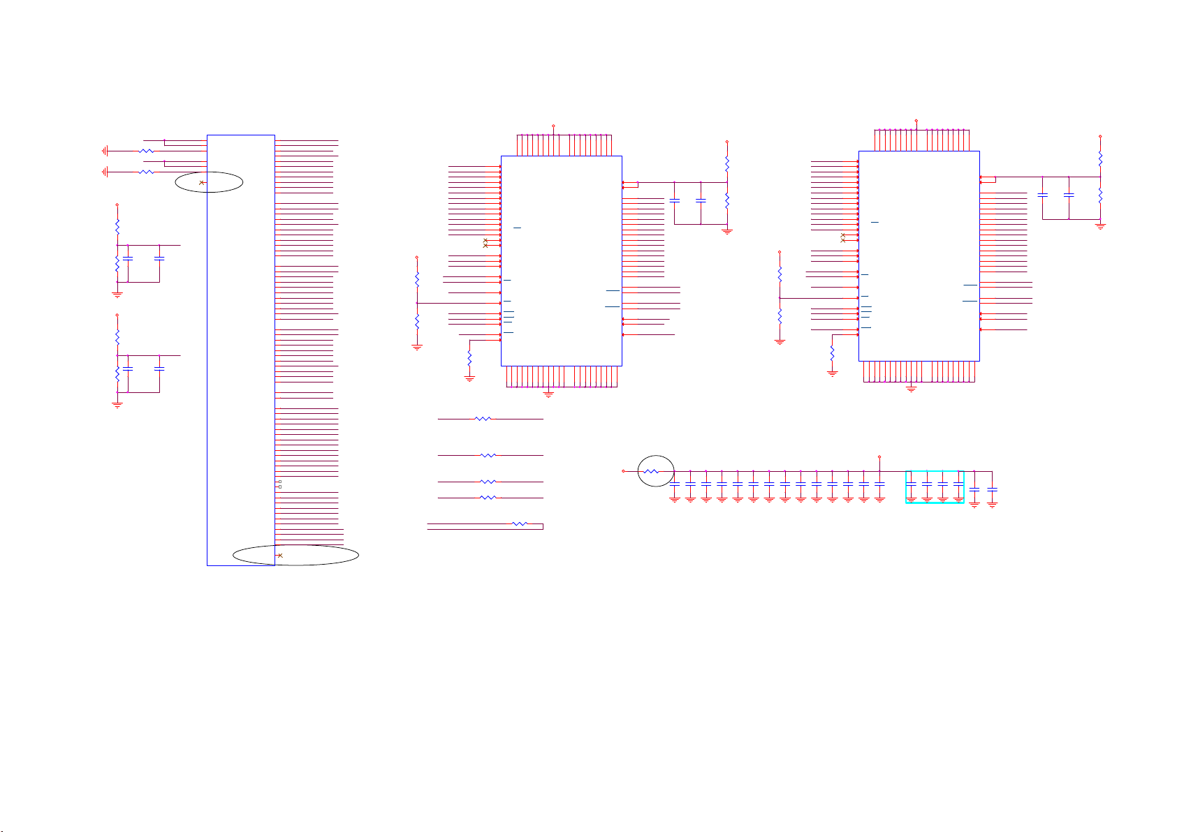
9-5-23 NT334e_DDR
connection)
NT334 DDR A-B
U5000A
A_VREF
B_VREF
CA5228
100N 16V
CA5233
100N 16V
R1
R2
T1
AB1
AB2
AC1
AC2
A_VREFCA
A_VREFDQ
A_ZQ
B_VREFCA
B_VREFDQ
B_ZQ
MLDO_OUT
VNT72334TBG
C_DQSLP
C_DQSLN
C_DQL0
C_DQL1
C_DQL2
C_DQL3
C_DQL4
C_DQL5
C_DQL6
C_DQL7
C_DQSUP
C_DQSUN
C_DQU0
C_DQU1
C_DQU2
C_DQU3
C_DQU4
C_DQU5
C_DQU6
C_DQU7
D_DQSLP
D_DQSLN
D_DQL0
D_DQL1
D_DQL2
D_DQL3
D_DQL4
D_DQL5
D_DQL6
D_DQL7
D_DQSUP
D_DQSUN
D_DQU0
D_DQU1
D_DQU2
D_DQU3
D_DQU4
D_DQU5
D_DQU6
D_DQU7
S_CLKP
S_CLKN
S_CASN
S_RASN
S_RESETN
SLDO_OUT
A_VREF
RA7584
240R 1%
B_VREF
RA7585
240R 1%
Updated on 2016/3/14
DDR_1.5V_AB
RA7583
1K 1/16W 1 %
CA5290
RA7575
RA7578
RA7587
DDR_1.5V_AB
1N 50V
CA5281
1N 50V
1K 1/16W 1 %
1K 1/16W 1 %
1K 1/16W 1 %
C_DML
C_DMU
D_DML
D_DMU
S_A0
S_A1
S_A2
S_A3
S_A4
S_A5
S_A6
S_A7
S_A8
S_A9
S_A10
S_A11
S_A12
S_A13
S_A14
S_A15
S_BA0
S_BA1
S_BA2
S_WEN
C_CSN
D_CSN
S_ODT
S_CKE
AJ7
C_DQSLP
AK8
C_DQSLN
AL5
C_DQL0
AJ11
C_DQL1
AM5
C_DQL2
AK12
C_DQL3
AK4
C_DQL4
AM13
AJ4
C_DQL6
AJ12
C_DQL7
AK11
C_DML
AM9
C_DQSUP
AL9
C_DQSUN
AJ10
C_DQU0
AJ6
C_DQU1
AM11
C_DQU2
AK6
C_DQU3
AJ9
C_DQU4
AM7
C_DQU5
AK10
C_DQU6
AL7
C_DQU7
AJ5
C_DMU
AJ19
D_DQSLP
AK20
D_DQSLN
AL17
D_DQL0
AJ23
D_DQL1
AM17
D_DQL2
AK24
D_DQL3
AK16
D_DQL4
AM25
D_DQL5
AJ16
D_DQL6
AJ24
D_DQL7
AK23
D_DML
AM21
D_DQSUP
AL21
D_DQSUN
AJ22
D_DQU0
AJ18
D_DQU1
AM23
D_DQU2
AK18
D_DQU3
AJ21
D_DQU4
AM19
D_DQU5
AK22
D_DQU6
AL19
D_DQU7
AJ17
D_DMU
AJ14
S_CLKP
AK14
S_CLKN
AG19
AH16
AG21
AG24
AG15
AH24
AF16
AH22
AG16
AH19
AG13
AH18
AH15
AH21
AF15
AF14
AG22
AH13
AF22
AG18
AF19
AF18
AF21
AL3
AK15
AF24
AF13
AJ25
S_BA0
S_BA1
S_BA2
S_CASN
S_RASN
S_WEN
S_RSTN
S_CS0N
S_CS1N
S_ODT
S_CKE
S_A0
S_A1
S_A2
S_A3
S_A4
S_A5
S_A6
S_A7
S_A8
S_A9
S_A10
S_A11
S_A12
S_A13
Updated on 2016/3/14
RA7591
NC/1K 1 /16W 1%
RA7576
NC/1K 1 /16W 1%
DDR_1. 5V_CD
S_A0
S_A1
S_A2
S_A3
S_A4
S_A5
S_A6
S_A7
S_A8
S_A9
S_A10
S_A11
S_A12
S_A13
S_BA0
S_BA1
S_BA2
S_CLKP
S_CLKN
DDR_S_CKE
DDR_S_CS0 N
S_RASN
S_CASN
S_WEN
S_ODT
S_CKE
S_CS0N
S_CS1N
S_RSTN
S_CLKP
S_CLKN
N3
A0
VDDB2VDDD9VDDG7VDDK2VDDK8VDDN1VDDN9VDDR1VDD
P7
A1
P3
A2
N2
A3
P8
A4
P2
A5
R8
A6
R2
A7
T8
A8
R3
A9
L7
A10/AP
R7
A11
N7
A12/BC
T3
A13
T7
A14
M7
NC_A15
M2
BA0
N8
BA1
M3
BA2
J7
CK
K7
CK
CL11(1600MHz)
K9
CKE
L2
CS
J3
RAS
K3
CAS
L3
WE
T2
RST
L8
ZQ
RA7582
240R 1%
VSSA9VSSB3VSSE1VSSG8VSSJ2VSSJ8VSSM1VSSM9VSSP1VSSP9VSST1VSST9VSSQB1VSSQB9VSSQD1VSSQD8VSSQE2VSSQE8VSSQF9VSSQG1VSSQ
NC = J 1,J9,L1,L9
DDR_S_ODT
RA7581
0R05 1/16W
DDR_S_CKE
RA7588
0R05 1/16W
DDR_S_CS0N
RA7589
0R05 1/16W
DDR_S_CS1N
RA7592
0R05 1/16W
RA7577
100R 1/16W 1%
DDR_1.5V_C D
R9
VDDQA1VDDQA8VDDQC1VDDQC9VDDQD2VDDQE9VDDQF1VDDQH2VDDQ
VREF_DQ
VREF_CA
DQU0
DQU1
DQU2
DQU3
DQU4
DQU5
DQU6
DQU7
UDQS
UDQS
CA5296
1N 50V
CA5288
DDR_1.5V_C D
N3
S_A0
RA7579
1K 1/16W 1 %
RA7586
CA5295
1K 1/16W 1 %
100N 16V
DDR_1. 5V_CD
RA7590
NC/1K 1 /16W 1%
CA5285
CA5278
22UF 6. 3V
22UF 6. 3V
CA5287
CA5301
100NF 16V
CA5293
CA5279
100NF 16V
100NF 16V
100NF 16V
DDR POWER CAP PLACE NEAR DDR IC
S_A1
S_A2
S_A3C_DQL5
S_A4
S_A5
S_A6
S_A7
S_A8
S_A9
S_A10
S_A11
S_A12
S_A13
S_BA0
S_BA1
S_BA2
S_CLKP
S_CLKN
DDR_S_CKE
DDR_S_CS1 N
S_RASN
S_CASN
RA7594
S_WEN
NC/1K 1 /16W 1%
S_RSTN DDR_S_ODT
CA5282
CA5277
CA5299
100NF 16V
100NF 16V
100NF 16V
A0
P7
A1
P3
A2
N2
A3
P8
A4
P2
A5
R8
A6
R2
A7
T8
A8
R3
A9
L7
A10/AP
R7
A11
N7
A12/BC
T3
A13
T7
A14
M7
NC_A15
M2
BA0
N8
BA1
M3
BA2
J7
CK
K7
CK
K9
CKE
L2
CS
J3
RAS
K3
CAS
L3
WE
T2
RST
L8
ZQ
RA7593
240R 1%
NC = J1,J9,L1,L9
DDR_1. 5V_CD
CA5300
CA5291
CA5297
100NF 16V
100NF 16V
100NF 16V
U5004
H9
K4B1G1646I-BCK0
H1
M8
E3
C_DQL0
DQL0
F7
C_DQL1
DQL1
F2
C_DQL2
DQL2
F8
C_DQL3
DQL3
H3
C_DQL4
DQL4
H8
C_DQL5
DQL5
G2
C_DQL6
DQL6
H7
C_DQL7
DQL7
D7
C_DQU0
C3
C_DQU1
C8
C_DQU2
C2
C_DQU3
A7
C_DQU4
A2
C_DQU5
B8
C_DQU6
A3
C_DQU7
F3
C_DQSLP
LDQS
G3
C_DQSLN
LDQS
C7
C_DQSUP
B7
C_DQSUN
E7
C_DML
LDM
D3
C_DMU
UDM
K1
DDR_S_ODT
ODT
G9
RA7610
FRC_1.5V
0 OHM 1/8W
DDR Layout notice:
1. Please refer to AN01 (Layout Guide).
2. Reserve the solder Mask free for some DDR
signals. (use for DDR tester probe
DDR_1.5V_C D
R9
VDDB2VDDD9VDDG7VDDK2VDDK8VDDN1VDDN9VDDR1VDD
CL11(1600MHz)
VSSA9VSSB3VSSE1VSSG8VSSJ2VSSJ8VSSM1VSSM9VSSP1VSSP9VSST1VSST9VSSQB1VSSQB9VSSQD1VSSQD8VSSQE2VSSQE8VSSQF9VSSQG1VSSQ
CAP C5247~C5250
PLACE at Layer4,
just for debug
use.
CA5298
CA5289
100NF 16V
100NF 16V
100NF 16V
VDDQA1VDDQA8VDDQC1VDDQC9VDDQD2VDDQE9VDDQF1VDDQH2VDDQ
VREF_DQ
VREF_CA
CA5284
CA5294
CA5280
100NF 16V
100NF 16V
DQL0
DQL1
DQL2
DQL3
DQL4
DQL5
DQL6
DQL7
DQU0
DQU1
DQU2
DQU3
DQU4
DQU5
DQU6
DQU7
LDQS
LDQS
UDQS
UDQS
100NF 16V
H9
LDM
UDM
ODT
U5006
K4B1G1646I-BCK0
H1
M8
E3
F7
F2
F8
H3
H8
G2
H7
D7
C3
C8
C2
A7
A2
B8
A3
F3
G3
C7
B7
E7
D3
K1
G9
CA5292
22UF 6. 3V
D_DQL0
D_DQL1
D_DQL2
D_DQL3
D_DQL4
D_DQL5
D_DQL6
D_DQL7
D_DQU0
D_DQU1
D_DQU2
D_DQU3
D_DQU4
D_DQU5
D_DQU6
D_DQU7
D_DQSLP
D_DQSLN
D_DQSUP
D_DQSUN
D_DML
D_DMU
CA5286
22UF 6. 3V
CA5229
1N 50V
DDR_1.5V_C D
CA5283
100N 16V
RA7574
1K 1/16W 1 %
RA7580
1K 1/16W 1 %

9-5-24 DCDCa_+1V0_+0V9
+12V
12
FB4100
30R 1A
C8159
C8167
10UF 16V
C8163
10UF 16V
10UF 16V
+5V_SW
C8169
10UF 16V
R4110
1 OHM 5%
+1V1-NT-OK
6
1
TP4129
C8177
BE-PWR-EN
+12V
5
2
TP4128
100NF 16V
R4111
100 OHM 1/16W
Novatek
6A DC/DC
Q4100
LMUN5313DW1T1G
3 4
R4103
10K 1% 1/16W
R4136
220K OHM
TP4127
C8175
100NF 16V
R4109
NC/ 47K 1/16W
R4114
R4135
100K 1/16W
+3V3
1
ZD4117
MM3Z5V6B
R4112
100K 1/16W
+1V1-NT-OK
100K 1/16W
100K 1/16W
R4134
220K 1%
3
Q4101
AO3416
2
R4116
TP4103
1
PGOOD
2
TRIP
3
EN
4
FB
RF5DL
R4139
47K 1% 1/16W
R4120
10K 1/16W
+3V3-NT
C8171
U4103
GND
BST
DH
LX
VCC
G5318RE1D
C8179
1NF
FRC _3.3V
10UF 16V
11
10
9
8
7
6
R4115
2.94K 1%
C8151
100NF 16V
R4117
R4132
R4140
10K 5% 1/16W
C8150
470PF 50V
R4122
0R05 OHM
10 OHM 1/16W
SENSE+0V9-NT
3R3 1/ 16W 5%
Vout=0.7*(1+3.6/10) = 0.952
AON7932
1
2
3
C8152
220pF 50V
U4102
G1
D1
D1
D14S2
S1/D29D1
10
8
G2
7
S2
6
S2
5
L4100
1uH
22uf 20% 6.3V
C8164
+5V_SW
C8168
22uf 20% 6.3V
BE-PWR-EN
SENSE+0V9-NT
C8174
+5V_SW
+0V9-NT
C8154
22UF 6.3V
SENSE+0V9-NT
+
100UF 16V
BE-PWR-EN
5,12,13,19, 20,24
FRC _0.9V
15
27
9-5-25 DCDCb_+1V5_+1V2
12
12
FB4101
30R 1A
C8157
+3V3-NT
Novatek
1A DC/DC
+12V
FB4102
30R 1A
C8160
10UF 16V
R4123
10K 5% 1/ 16W
L4101
1.5uH
SENSE+2V5-NT
C8153
C8156
DDRV
100NF 16V
C8173
1UF16V
C8165
10UF 16V
10UF 16V
1NF
C8170
R4124
NC/ 27K 1/16W 5%
1
2
3
2.2nF 50V
U4100
GND
EN
VIN
FB
BOOT
PVCC
SW
SS4GND
RT7277GSP
R4121
9
8
7
6
5
C8172
100NF 25V
0.765Vref
Updated to 1% on 2015/9/3
R4133
33K 1%
150K OHM 1% 1/ 16W
R4131
12K 1% 1/16W
27
C8155
22UF 20% 6.3V
C8161
100pF 50V
R4125
68K 1/16W 1%
C8158
22UF 20% 6.3V
C8162
22UF 20% 6.3V
+2V5-NT+12V
+
C8166
100UF 16V
FRC _2.5V
5
+3V3-NT
R4137
47K 1/16W
6
1
C8178
47NF 16V
2
Q4105
LMUN5313DW1T1G
3 4
R4118
10K 5% 1/16W
R4138
220K OHM
C8176
100NF 16V
1
3
2
ZD4102
MM3Z5V6B
Q4104
AO3416
FRC_1.5V
9.6 J 715G8623 IR/LED Panel
9-6-1 IR
CN201
NC/C ONN
10 11
NC/C ONN
10 11
CN203
67
CONN
1
2
3
4
5
6
7
8
9
1
2
3
4
5
6
7
8
9
1
2
3
4
5
CN202
LED_R
RC-I R
LS_SCL
LS_SDA
LED_R
RC-I R
LS_SCL
LS_SDA
LED_R
RC-I R
3V3SB
DVD3V3
3V3SB
DVD3V3
ZD200 ZD201 near U212 pin
3V3SB
IR_power
RC-I R
ZD200
AZ5123-01H
ZD201
AZ5123-01H
12
1 2
U212
1
GND
2
VCC
3
Vout
4
GND
TSOP75436TR
Light Sensor
LS_SCL
LS_SDA
DVD3V3
R225 0R05 1/16W
R222
R221
R226 NC/0R 05 1/16W
10K 1/16W 5%
10K 1/16W 5%
DVD3V3
R223
R224
0R05 1/16W
NC/ 0R05 1/16W
C222 1uF 10V
C221 100N 16V
U221
JSA-1130
1
ADDR
2
VDD
SDA
GND3SCL
6
INT
5
4
R223
JSA-1130
NC 0x44
JSA-1130 0RNC0R
TSL25715
Digital Light Sensor
R225R224 R227R226
NCNC0R0R
0R0RNCNC0R
R227 NC/0R 05 1/16W
R228 0R05 1/16W
R229 0R05 1/16W
NC
LS_SDA
LS_SCL
I2C ADDR
R229R228
0R0R
0x45NCNC
0R0R
0x29
NC
Standby LED
C211
1UF 6.3V
3V3SB
R211
100R 1/16W 5%
C212
NC/ 1UF 6.3V
IR Receiver
IR_power
LED_R
1K 1/16W 5%
LED201
GPSS008RC4
Red
R202
3V3SB
12
R201
10K 1/16W 5%
Q201
BC847BW
ZD203 NC /AZ5123-01H
ZD202 NA/ AZ5123-01H
1 2
1 2
ZD202 ZD203 near LED201
 Loading...