

Page 1
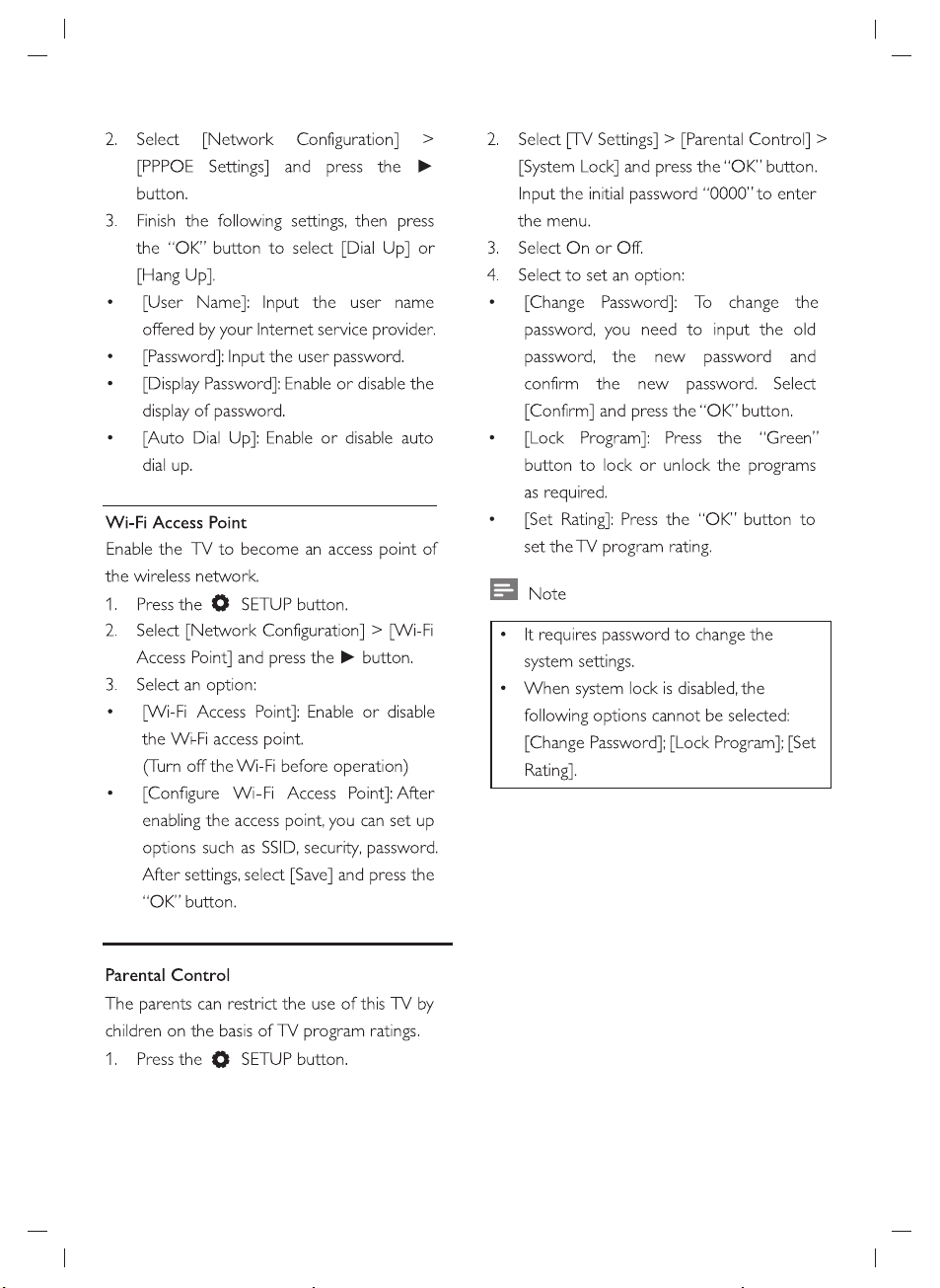
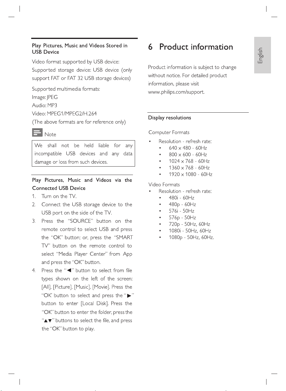
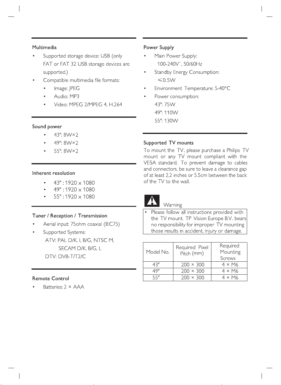
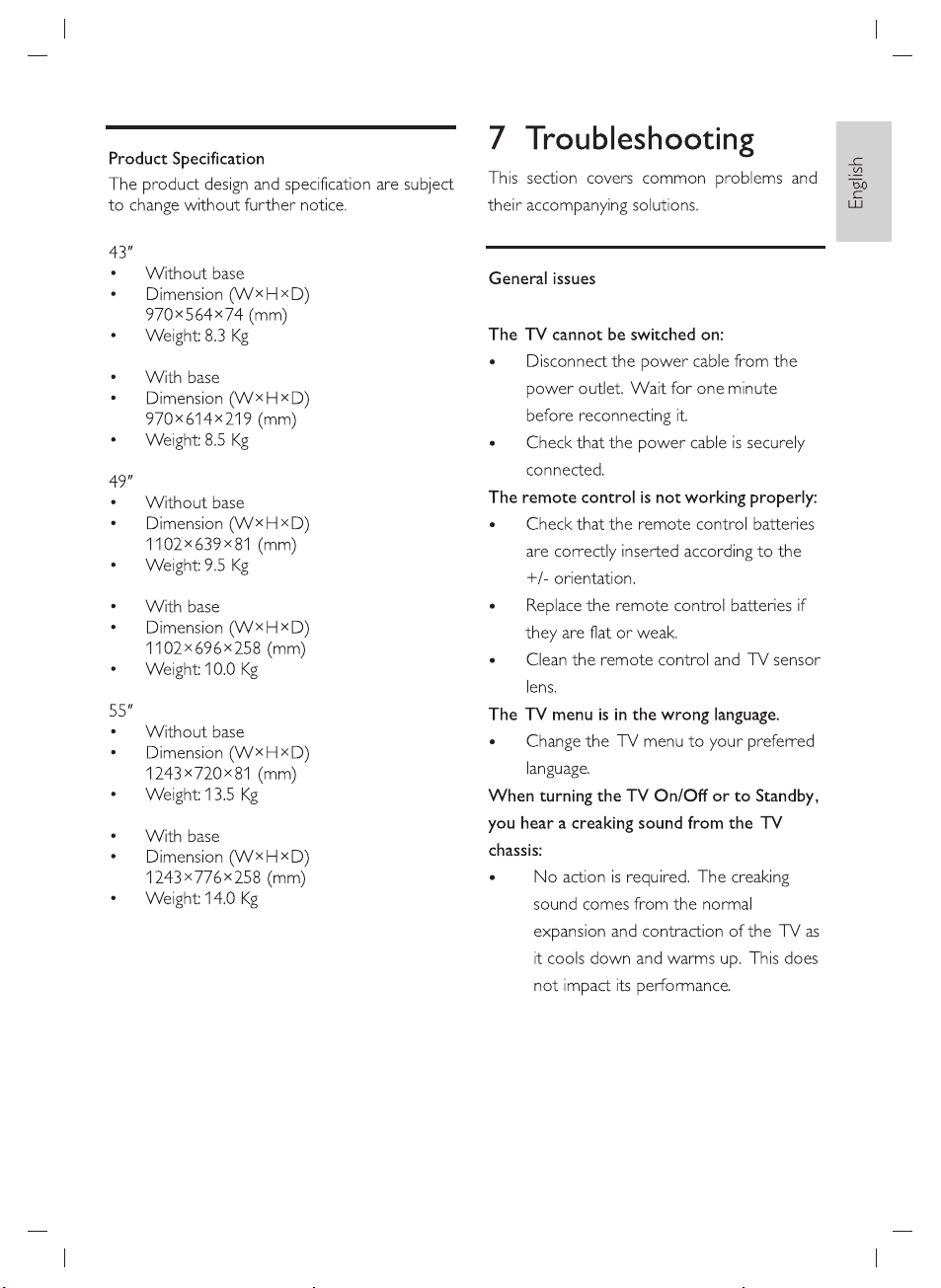
Colour Television Chassis
43PFT6110S/67
49PFT6100S/56
Product Specification Sheet (Page1-15)
User Manuel Part(Page16-51)
Troubleshooting Procedure(Page52-57)
Factory Mode Adjustment (Page58-60)
Software Upgrades(After Service)(Page61-71)
Main Board Circuit Diagram (Page72-79)
Page 2
Product Specification Sheet
43" FHD STV(43S91F-DVB) 49" FHD STV(49S91F-DVB)
Series name
Set Product Manager
Set Product Manager in outsourcing company
E-mail address of main contact in outsourcing
company
Set Project Manager
Status
CR (yyyyww) of leading set
Platform/Chipset T8E3-6A628 DVB-T2 T8E3-6A628 DVB-T2
Processor type (CPU) / GPU
RC
Backlight Type (Panel Supplier)
Diagonal Screen Size
Perfect Motion Rate
Panel Frequency (Native)
Chasis Frequency
Backlight Dimming
Scanning Segments (amount)
Panel Resolution
Aspect ratio
Brightness (Home Vivid Mode) cd/m² Min:180cd/m2,Typ:210cd/m2
Panel contrast ratio
48.25--863.25MHZ 48.25--863.25MHZ
TBC TBC
TBC TBC
DLED DLED
42.51" 48.5"
60HZ 60HZ
60HZ 60HZ
PWM PWM
1920*1080 1920*1080
16:9 16:9
Min:280cd/m2 ,Typ:330cd/m2
1200:1 1200:1
1
Page 3
Viewing Angle - H (L+R)
Viewing Angle - V
Response Time (ms)
Analog + PWM dimming
2D/3D Logic (2D/3D Active/3D Passive)
Color Gamut
PQ engine
PQ Resolution
3D features
Improved 3D Super Resolution
ISF Color Management
Digital Natural Motion (2D/3D)
Perfect Natural Motion (2D/3D)
2D to 3D Conversion
3D Depth adjustment (Auto/Offset)
Auto 3D Detection
Micro Dimming Demo
Micro Dimming mode
Dual View (2 Player Full Screen Gaming/Video)
Supported Display Resolution (Computer
178° 178°
178° 178°
8ms 9ms
YES YES
2D 2D
NTSC 66% NTSC 65%
Digital Crystal Clear Digital Crystal Clear
N/A N/A
N/A N/A
N/A N/A
N/A N/A
N/A N/A
N/A N/A
N/A N/A
N/A N/A
N/A N/A
N/A N/A
N/A N/A
720*400@70HZ
N/A N/A
720*400@70HZ
Supported Display Resolution (Video Inputs) 480i, 480p,576i,
Brightness (Shop Vivid mode: 10% boost)
Pixel Plus Link (I/II/III)
Active Control
YES(1% boost) YES(1% boost)
N/A N/A
N/A N/A
2
480i, 480p,576i,
Page 4
Natural Motion/Perfect Natural Motion
"UHD Display" - logo (Industry)
"UHD Receiver" - logo (Industry) -pending std
HDMI 2.0 4:4:4 @ 60p
10-bit color support
DAPQ
Ambilight
Ambilight Version
Pixels
Ambilight Performance (nit, no of colors, halo
Ambilight Features (Wall colour adaptive,
Ambilight for 3D
Ambilight for all TV Events
Ambilight Open Source via JointSpaceApp
Wall Distance Adaptive (Stand vs Mount)
Motion Adaptive
Built-in AL + Hue
TV as Lamp(s) in Hue ecosystem
In screen demo in mobile shop app
Ambi Wakeup (ref HTV)
Ambimusic
N/A N/A
N/A N/A
N/A N/A
N/A N/A
N/A N/A
N/A N/A
N/A N/A
N/A N/A
N/A N/A
N/A N/A
N/A N/A
N/A N/A
N/A N/A
N/A N/A
N/A N/A
N/A N/A
N/A N/A
N/A N/A
N/A N/A
N/A N/A
Sound (TV)
Sound (Internal)
Output Power (10% THD) RMS
16W 16W
3
Page 5
Speaker configuration
Speaker system
Speaker type
Auto Volume Levelier / Auto Volume Levelier +
Sound Claim (Incredible Surround/Cinema
Surround/Clear Sound/AmbiwOOx/3D
Bass (Bass control/DBE/Ultra Bass/Ultra Bass
Wireless Sound Interface
Dolby Digital DecoderType
DTS Studio Sound
DTS 2.0+ Digital out
Acoustic Compensation Filters
Dynamic Treble Enhancement
Programmable Bass And Treble Curve
Visible Sound
Sound (External)
External Sound device type
Output Power (10% THD) RMS
8W+8W 8W+8W
2.0 2.0
built-in(normal) built-in(normal)
YES YES
N/A N/A
N/A N/A
N/A N/A
YES YES
N/A N/A
N/A N/A
N/A N/A
N/A N/A
N/A N/A
N/A N/A
N/A N/A
N/A N/A
Design Specs
Stand type (Swivel/non Swivel)
Metal Bridge Metal Bridge
I/O port to be clearly indicated RJ45*1/HDMI*3/VGA*1/AV-
Local Keyboard
Philips wordmark
Leading Edge
YES YES
AOC AOC
N/A N/A
4
RJ45*1/HDMI*3/VGA*1/AV-
Page 6
Vesa Wall Mount Compatible
Compatible Wall Mount
POS label
Connectivity (I/O)
HDMI Number
HDMI 1.4a
HDMI 2.0
HDMI/DVI
HDMI ARC
EasyLink (HDMI-CEC)
Scart (EU) Connections
YPbPr/CVI (EU/Latam) Connections
CVBS (EU/Latam) Connections
Audio L/R in
CI+ slots
Antenna
Satellite (for K&S only)
USB
USB Harddisk Format (Power)
VGA
VGA/DVI Audio Input
Digital audio out (SPDIF)
Headphone
Ethernet-LAN RJ-45
YES YES
200mm*300mm 200mm*300mm
*3(HDMI3 support MHL) *3(HDMI3 support MHL)
HDMI(Side-out/Under-out) HDMI(Side-out/Under-out)
N/A N/A
YES YES
HDMI-2 HDMI-2
YES YES
N/A N/A
N/A N/A
*1 *1
*1 *1
*1 *1
*1 *1
N/A N/A
USB2.0/USB3.0 USB2.0/USB3.0
FAT FAT
YES YES
share AV audio input share AV audio input
N/A N/A
*1 *1
*1 *1
5
Page 7
Service Connector
Wireless connections
Wi-Fi Band Concurrent
WoWLAN
WoLAN
Bluetooth for subwoofer/RC (do not claim
Multichannel over BT
HDCP v2.2 (on HDMI 2.0 port)
MHL (HDMI+power+return channel)
Wi-fi Miracast Certified (HDCP 2.2 supported)
GoogleCast Receiver
Tablet Screen Mirroring (Wi-Fi Miracast)
TAD AppFTA channels (free app)
TAD Server, FTA channel
Indep. Watching (TV&PVR), FTA&CI+
SAT>IP Client, FTA
HEVC @ FHD 60Hz
HEVC @ UHD 60Hz
H264 @ UHD
VP9 @ UHD
VGA connectable VGA connectable
YES YES
N/A N/A
N/A N/A
N/A N/A
N/A N/A
N/A N/A
N/A N/A
YES YES
N/A N/A
N/A N/A
N/A N/A
N/A N/A
N/A N/A
N/A N/A
N/A N/A
N/A N/A
N/A N/A
N/A N/A
N/A N/A
UI & Interaction
Ux (Basic: without Dashboard, Advanced: with
Animations
Drag and drop
Basic Basic
N/A N/A
N/A N/A
6
Page 8
Remote Control Version (state if include
Keyboard/Pointer)
Sensor.accelerometer & sensor gyroscope
Easy access to eDFU (Blue key)
Text Entry (Basic : Text Entry via HID and/or
On-screen Keyboard)
N/A N/A
N/A N/A
N/A N/A
Basic Basic
Multi-view
Multi-task
N/A N/A
N/A N/A
Screen Format Adjustments wide screen; 4:3; movie expand16:9;
Dual Screen (TV and TeleText)
Teletext
e-Sticker
Priority Channel List
Channel Cloning via USB
Logo Editor (Channel Editor)
Channel Matrix with EPG data
Channel Scanning (Australia/NZ)
Time Zone (Australia/NZ)
PC Sorting
Intelligent Source List
On-screen Remote (via HDMI)
Cold boot to broadcast
Cold boot to online dashboard
Warm boot to broadcast
Warm boot to online dashboard
N/A N/A
N/A N/A
N/A N/A
N/A N/A
N/A N/A
N/A N/A
N/A N/A
N/A N/A
N/A N/A
N/A N/A
N/A N/A
N/A N/A
N/A N/A
N/A N/A
N/A N/A
N/A N/A
wide screen; 4:3; movie expand16:9;
7
Page 9
Zapping OSD with EPG data
Electronic Program Guide (IP & Broadcast)
8 Days Electronic Program Guide
Live Setting Assistant (include PQ level)
Signal Strength Indication
Pause TV/USB recording (PVR)
Two simultaneous recordings in stdby
N/A N/A
N/A N/A
YES YES
N/A N/A
YES YES
YES YES
N/A N/A
UI Languages English, Malaysia, Indonesian, Thai,
English, Malaysia, Indonesian, Thai,
Memory Profile (DRAM)
Menu Layout Update
Wizards (Ease of Installation)
Single Sign On (google a/c only)
Personalized Dashboard
Face recognition
Shopmode 2015
CloudTV app content in search and Dashboard
Firmware Upgradeable
512M 512M
N/A N/A
N/A N/A
N/A N/A
N/A N/A
N/A N/A
N/A N/A
N/A N/A
YES YES
Multimedia Applications
Video Playback Formats MJPEG,MPEG-1,MPEG-2,MPEG-
Subtitles Formats Support
Music Playback Formats
Picture Playback Formats
Smart TV
MP2/MP3/AAC/M4A/PCM MP2/MP3/AAC/M4A/PCM
SRT、ASS SRT、ASS
JPG/JPEG/PNG/BMP JPG/JPEG/PNG/BMP
YES YES
MJPEG,MPEG-1,MPEG-2,MPEG-
Software Platform N/A N/A
8
Page 10
Android Home Page N/A N/A
Android OS N/A N/A
UI Resolution N/A N/A
Google Voice Search N/A N/A
Google Hangouts N/A N/A
Remote Control N/A N/A
Gesture N/A N/A
Pre-installed Google Apps (Google Search,
N/A N/A
Basic Performance Profile N/A N/A
Google Play N/A N/A
Memory size to install apps N/A N/A
Extendable USB storage for App Download N/A N/A
Smart TV Experience N/A N/A
DLNA 1.5 - DMR, DMP N/A N/A
DLNA 1.5 - DMS N/A N/A
MultiRoom Client, FTA+Scrambled Non-Copy
MultiRoom Server, FTA+Scrambled Non-Copy
N/A N/A
N/A N/A
PVR Auto Recording (IP-EPG) N/A N/A
API - access control N/A N/A
xTV Support N/A N/A
Rich User Interaction N/A N/A
Smart Home N/A N/A
4k photo support in Android apps N/A N/A
4k photo support in Picture apps N/A N/A
9
Page 11
4k photo support in USB/DLNA N/A N/A
UHD content playback from all sources
N/A N/A
NextFlix UHD N/A N/A
Youtube UHD N/A N/A
Google Play UHD N/A N/A
Smart TV with Broadcast PIP; single video N/A N/A
SMART TV offline content (cached) N/A N/A
MPEG-DASH (CENC & CFF) N/A N/A
HLS N/A N/A
Wake up from APP N/A N/A
Preinstalled Apps N/A N/A
Netflix * N/A N/A
YouTube Leanback (HTML5) * N/A N/A
Spotify * N/A N/A
BBC iPlayer * N/A N/A
Skype N/A N/A
Skype Cowatch (mix audio) N/A N/A
Cloud Explorer N/A N/A
Cloud TV N/A N/A
Smart TV Services N/A N/A
Social Apps N/A N/A
Game Dashboard in Google launcher N/A N/A
OpenGL Games N/A N/A
Playstation Now App N/A N/A
10
Page 12
OnLive App N/A N/A
STA 3.0 & 4.0 Clients N/A N/A
STA shared App store N/A N/A
Camera & Mic API N/A N/A
TV as an app (Verimatrix, etc) N/A N/A
Companion Apps N/A N/A
Philips TV Remote App N/A N/A
Sharing in Remote App N/A N/A
Ambilight TV App N/A N/A
Ambilight+Hue App N/A N/A
User Manual App N/A N/A
Channel Editor - PC Client App N/A N/A
Mobile app for in-shop (cover MRA/Demo
Proximity based shop app activation
N/A N/A
N/A N/A
MyRemote App (Old TV Remote App) N/A N/A
Ambilight Lounge App N/A N/A
Broadcast/Certification
DVB-T/C
DVB-S/S2
DVB-T/T2
DVB-C2
SBTVD-T (Brazil)
SATVD-T (Argentina)
YES YES
N/A N/A
YES YES
N/A N/A
N/A N/A
N/A N/A
11
Page 13
Analog (LATAM/APMEA)
Nicam (APMEA)
Enhanced SSU
Italy HD Book 2.1.1 (GOLD)
HD-Book Italy 3.0 (HEVC@FHD)
UK D Book 7a
Freeview SD (UK)
Freeview HD (UK)
MHEG 5(only HbbTV)
TiVuON (IT)
TNT HD (FR)
Argentina Ginga - NCL
Brazil Ginga (A/B)
Video Playback
Dual Cam (CI+)
Dual Tuner
CI+ 1.4 Multistream CAM
CI+ 1.3 CAM
HBBTV 1.5
HBBTV 2.0
MHP
Ziggo Interactief
3D DVB Phase 1
3D signaling bits in broadcast
PAL SECAM NTSC PAL SECAM NTSC
N/A N/A
N/A N/A
N/A N/A
N/A N/A
N/A N/A
N/A N/A
N/A N/A
N/A N/A
N/A N/A
N/A N/A
N/A N/A
N/A N/A
N/A N/A
N/A N/A
N/A N/A
N/A N/A
N/A N/A
N/A N/A
N/A N/A
N/A N/A
N/A N/A
N/A N/A
N/A N/A
12
Page 14
Background update installation
Marlin/ Play ready
N/A N/A
N/A N/A
Sustainability/Power
PVC / BFR Free
Mercury Free
Cabinet Resin
Eco-Flower Certified
ECO Mode
Mains Power
Standby Power
Quick Startup
Network Standby mode (max 6W)
Off Mode Power
AC 100-240V 50/60Hz AC 100-240V 50/60Hz
N/A N/A
N/A N/A
Metal Metal
N/A N/A
N/A N/A
<0.5W <0.5W
NA NA
NA NA
<0.5W <0.5W
On Mode Power (Consumption Power) 130W (max.) 130W (max.)
Auto Switch-Off Timer
Green packaging (Non-EPS)
Light Sensor
Picture Mute (For Radio)
EU Energy Label (A++/A+/A/B) - Requirement
non-EU Energy Label - Standby Label (A/B/C)
Blauer Engel (Germany)
Accessory
By-packed accessories
Active Glasses (509)
N/A N/A
N/A N/A
N/A N/A
NA NA
NA NA
NA NA
N/A N/A
N/A N/A
13
Page 15
Active Glasses (529)
Passive Glasses (PTA417)
Dual Gaming Glasses
Woofer (e.g. SWB50) with Soundbeam
Sound Bar
Detachable speaker base 可拆卸喇叭
Wireless audio adaptor
Wi-Fi Adapter (PTA01/00/PTA127/55)
Skype Camera (PTA317)
Table Stand
N/A N/A
N/A N/A
N/A N/A
N/A N/A
N/A N/A
N/A N/A
N/A N/A
N/A N/A
YES YES
YES YES
Accessory Bag
Mains Cord (EU/UK/Brazil/APMEA)
Remote Control + 2x Philips Batteries
Printed QSG
YES YES
YES YES
YES YES
YES YES
EDFU (APMEA) YES YES
Safety Legal Leaflet (EU) - 3D Health Advise
N/A N/A
Philips Warranty Leaflet
Optional accessories
Active Glasses (PTA509/529)
Passive Glasses (PTA419)
Dual Gaming Glasses (PTA436)
Wi-Fi Adapter (PTA01/00/PTA127/55)
Skype Camera (PTA317)
Table Top Stand
N/A N/A
N/A N/A
N/A N/A
N/A N/A
N/A N/A
N/A N/A
N/A N/A
14
Page 16
Speaker stand
N/A N/A
Others
Certification
Dolby Digital/Dolby Digital Plus/Dolby Pulse N/A N/A
DTS 2.0+ Digital out
DTS Premium Sound
DivX
WMA
Wi-Fi N/A N/A
DLNA Certified (DMR/DMP/DMS)
SKYPE
HDMI
MHL
Dimensions (WxHxD)
Unit with stand 970*617*227mm 1102*696*227mm
Unit without stand 970*564*74mm 1102*639*81mm
Carton 1085*667*150mm 1210*744*175mm
Wall-mount 200*300 mm 200*300 mm
Weight
Product without Stand 8.2Kg 9.7Kg
Product with Stand 8.5Kg 10.0Kg
Product in Packaging 10.5Kg 13.5Kg
15
Page 17
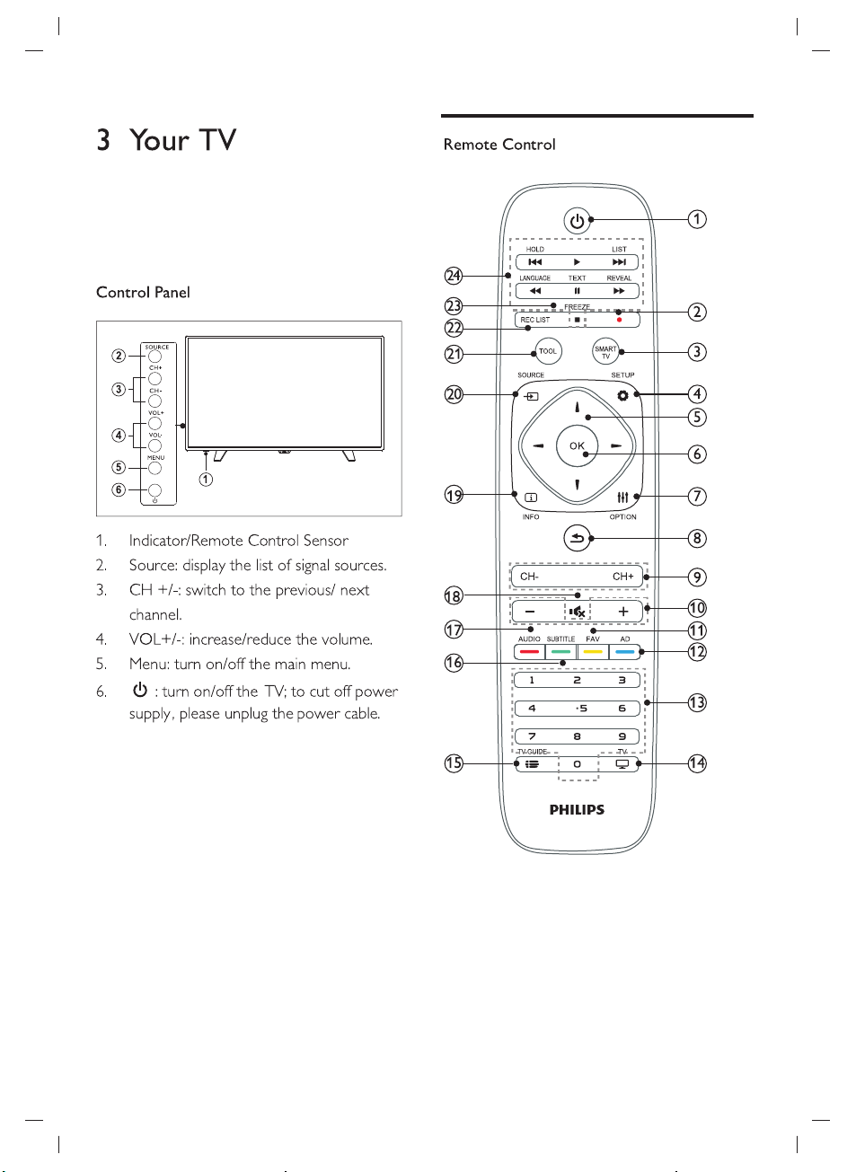
43PFT6110S/67
16
Page 18
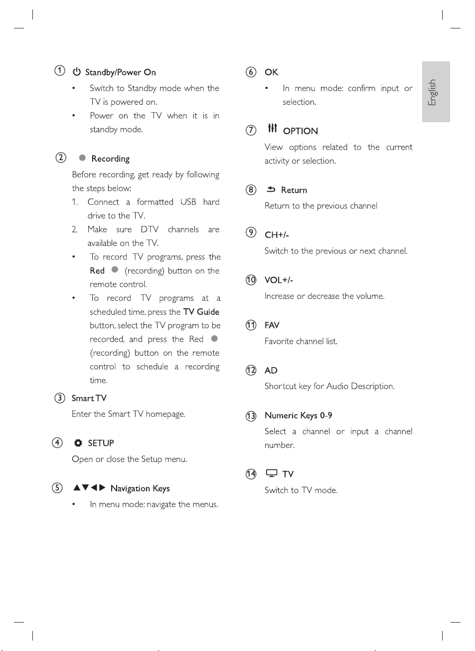
17
Page 19
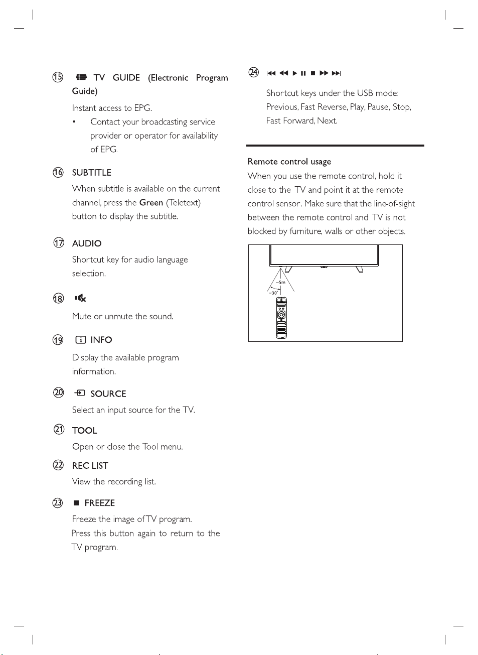
18
Page 20
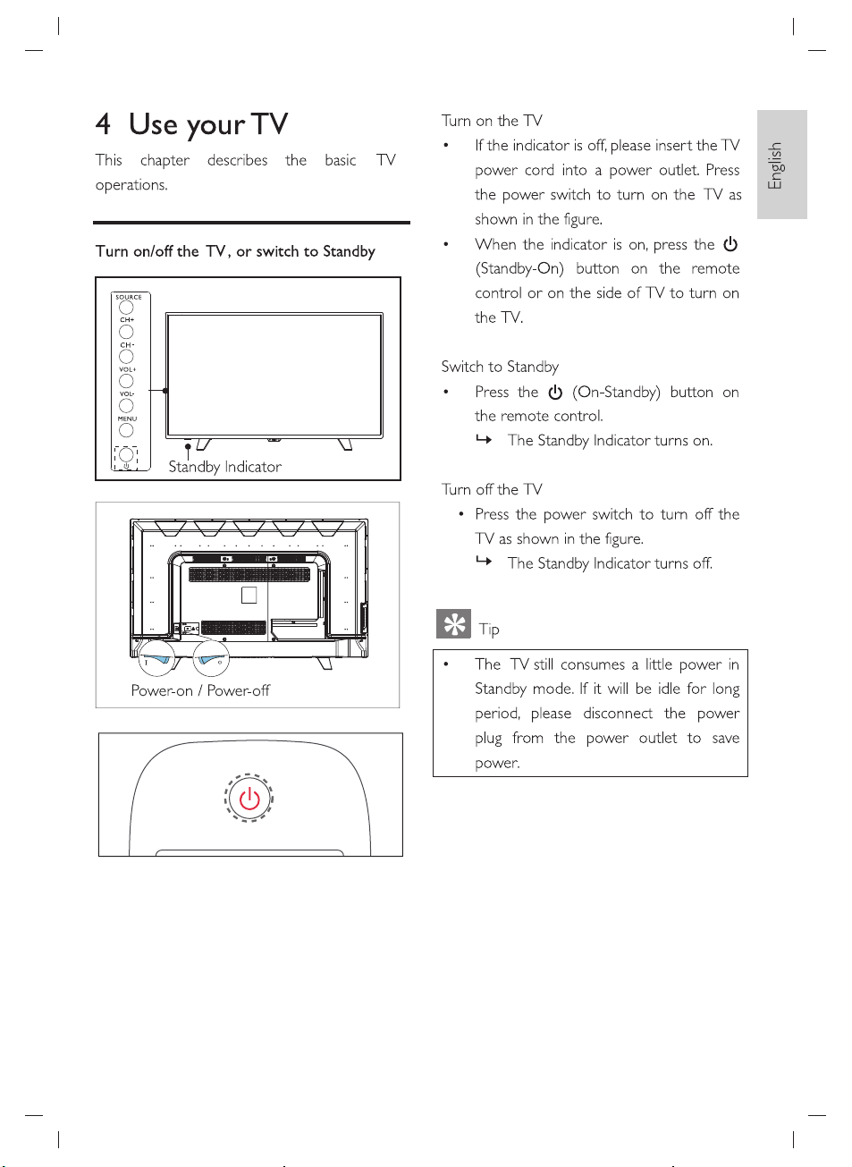
19
Page 21
20
Page 22
21
Page 23
22
Page 24
23
Page 25
24
Page 26
25
Page 27
26
Page 28
27
Page 29
282930
Page 30
Page 31
Page 32
31
Page 33
32
Page 34
33
Page 35
49PFT6100S/56
34
Page 36
35
Page 37
36
Page 38
37
Page 39
38
Page 40
39
Page 41
40
Page 42
41
Page 43
42
Page 44
43
Page 45
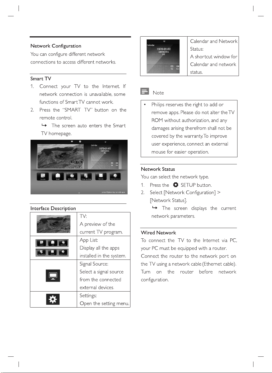
44
Page 46
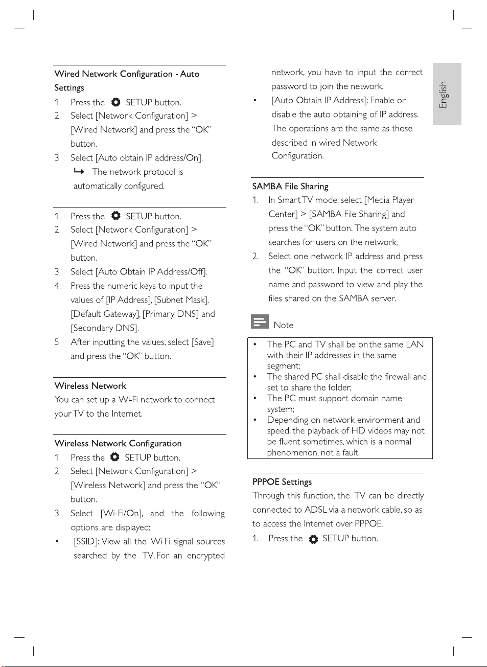
45
Page 47
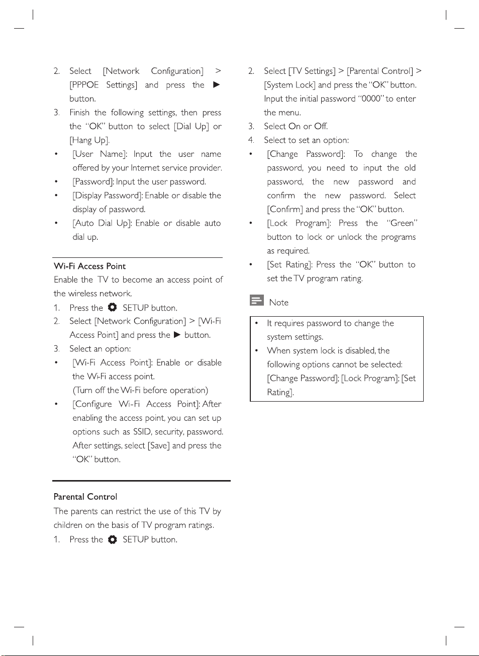
46
Page 48
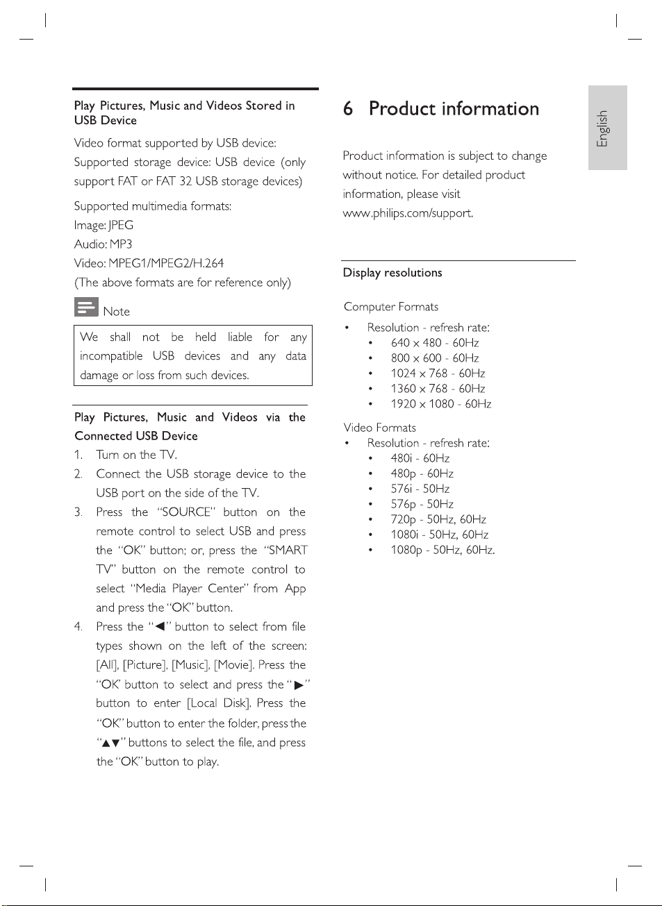
47
Page 49
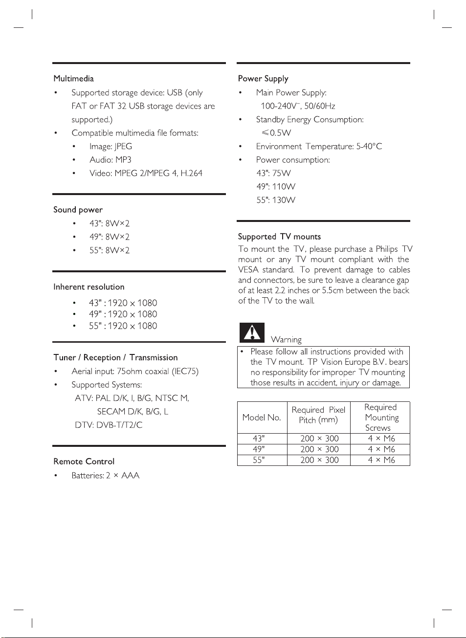
48
Page 50
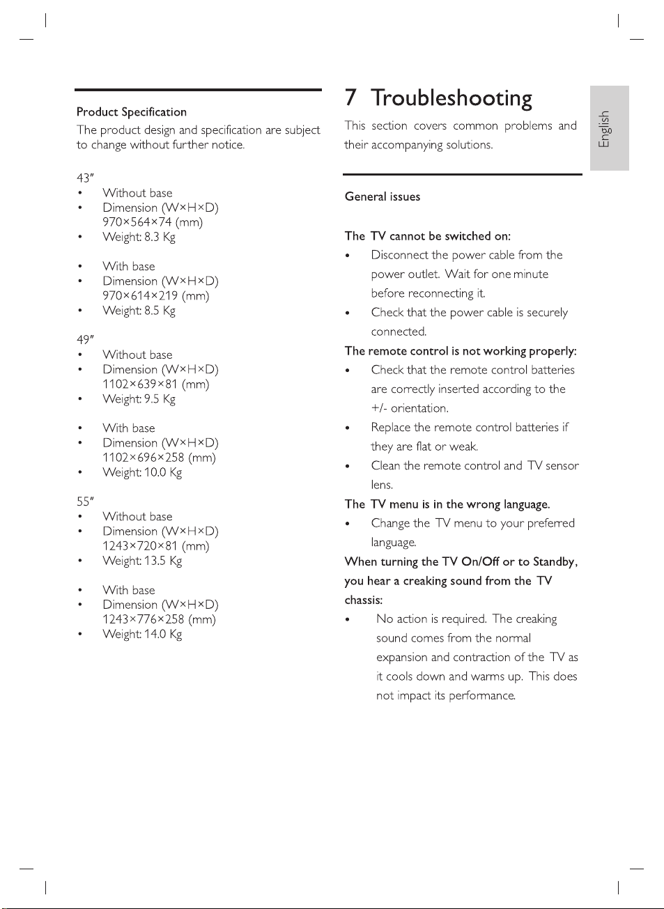
49
Page 51
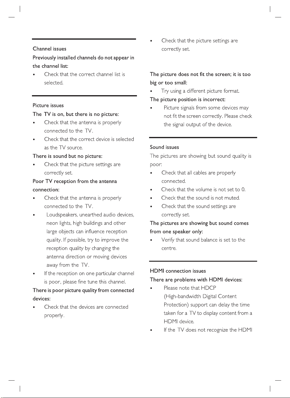
50
Page 52
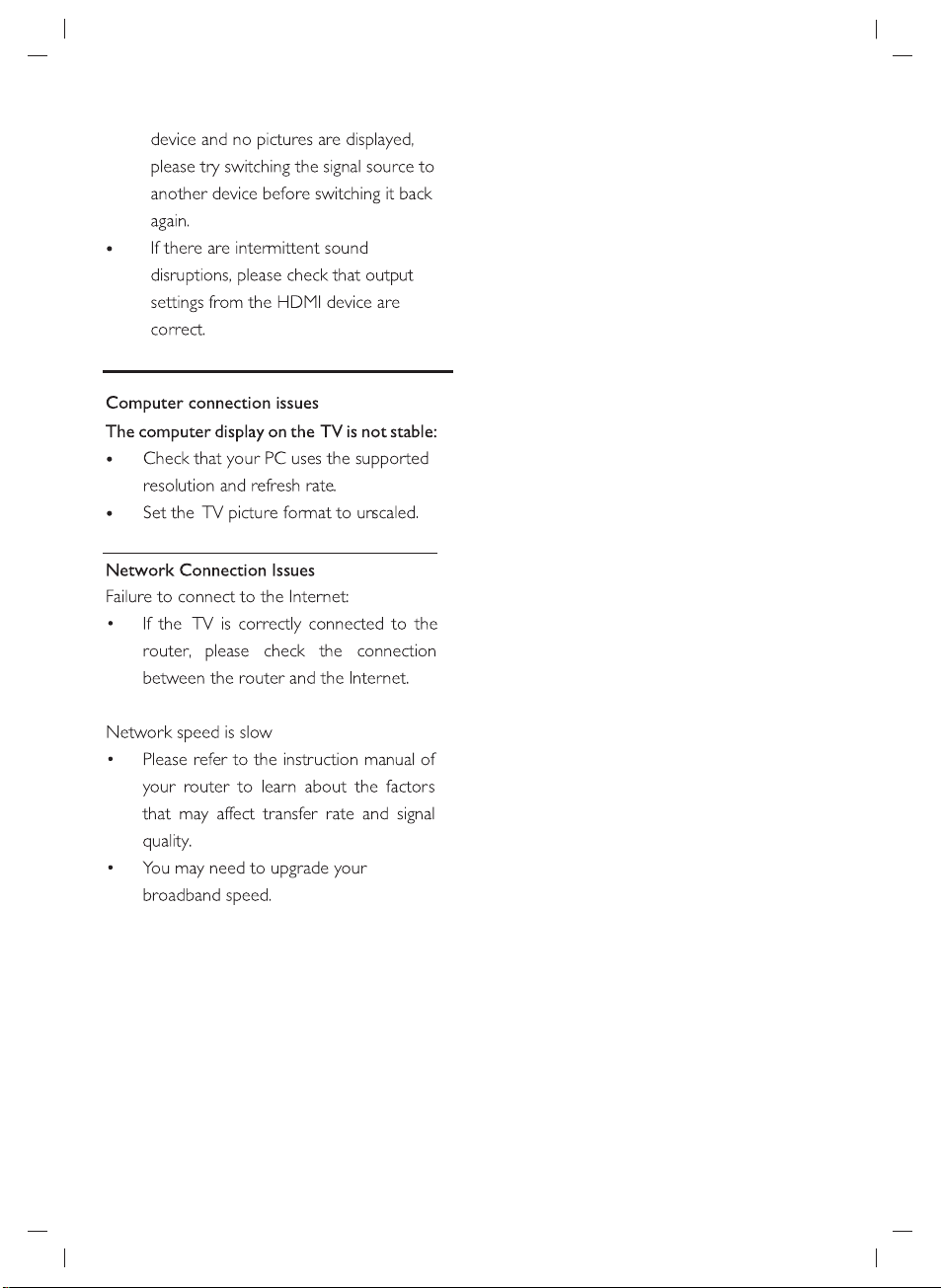
51
Page 53
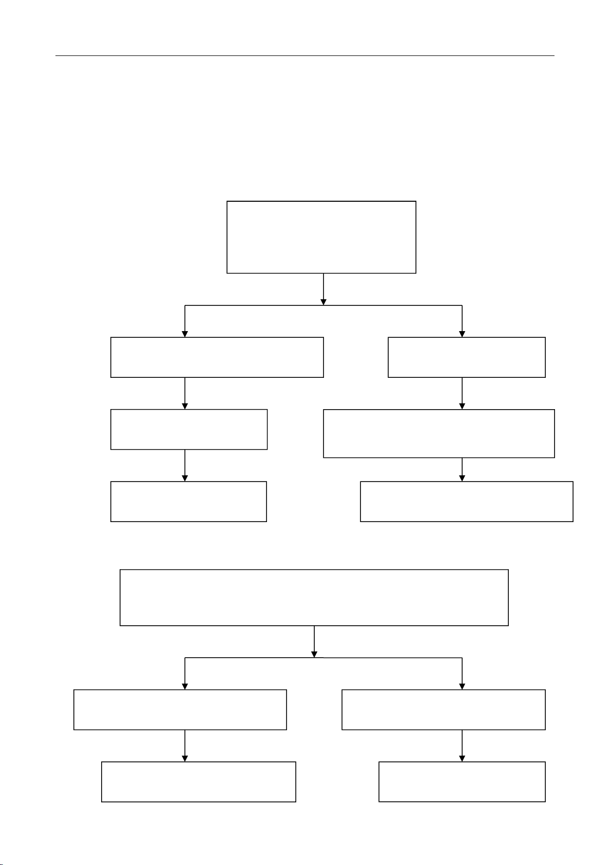
Document: After-sales Maintenance Service Manual No.: T7** Version: 3.0 Effective from: March15th, 2010
Page of 14 KTC
1
After-sales Maintenance Service Manual
Date: March 2010
1. No power
2. Without light
Check 220V power supply voltage
and the contact of power socket
Check AC( 220V )voltage and the
contact of CN101 socket.
Check +5V and +12V output from
embedded power supply for abnormity
Check +5V and +12V on
main board for abnormity
Replace power cord or power
socket
Check for open-loop of fuse,
or replace main board
Check main board of power supply for
looseness, open-loop and poor contact
YES
NO
YES
NO
YES
NO
When the indicator is on but there is no display, check remote control for
power-off, minimum brightness, contrast ratio, check high-voltage switchboard
controlled by main board for abnormity
Check the fuse on high-voltage board for
the supply of 12V
Check each triode of control part for
abnormity or replace main board
Replace high-voltage switchboard
Check fuse
YES
YES
NO
NO
Abnormal output voltage +5V and +12V from
embedded power supply, replace embedded
power supply with the same model
Troubleshooting Procedure
52
Page 54
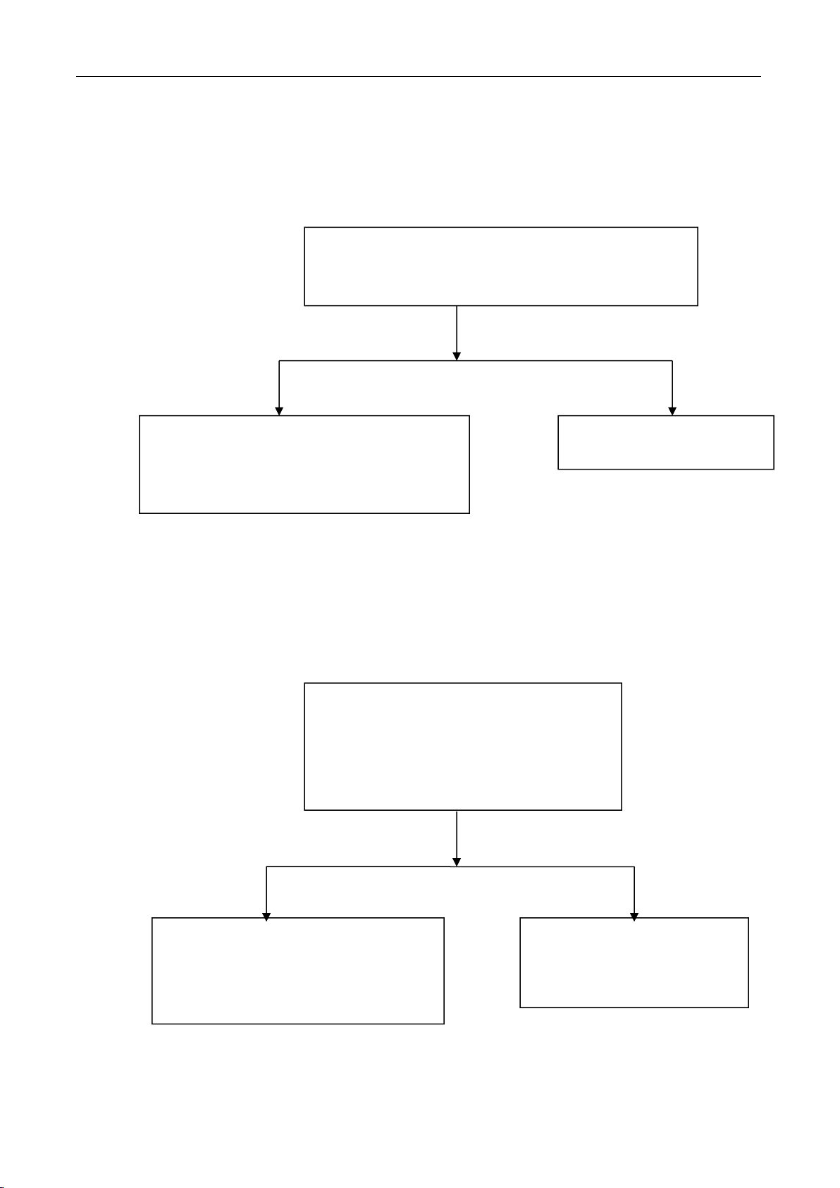
3. Protection or without light (refers to the disappearance of image several seconds
after the emergence of image)
4. White panel
The image disappeared immediately after the
emergence; check the plug of high-voltage switch board
for striking sparks and poor contact
No problems identified, replace high-voltage
board; if the fault remains, check the contact
line of back light of LCD for any damage, and
replace LCD board.
If there is spark striking,
replace high-voltage board
YES
NO
White panel refers to the back light works
without visible signal and just show white
screen. Check the voltage of socket for flat
cable connecting the main board to screen
for abnormality
Check the interface between main board
and connect line for any looseness,
shedding, if no abnormity existed,
replace LCD screen
Check the power supply chip of
control screen or replace main
board
YES
NO
53
Page 55
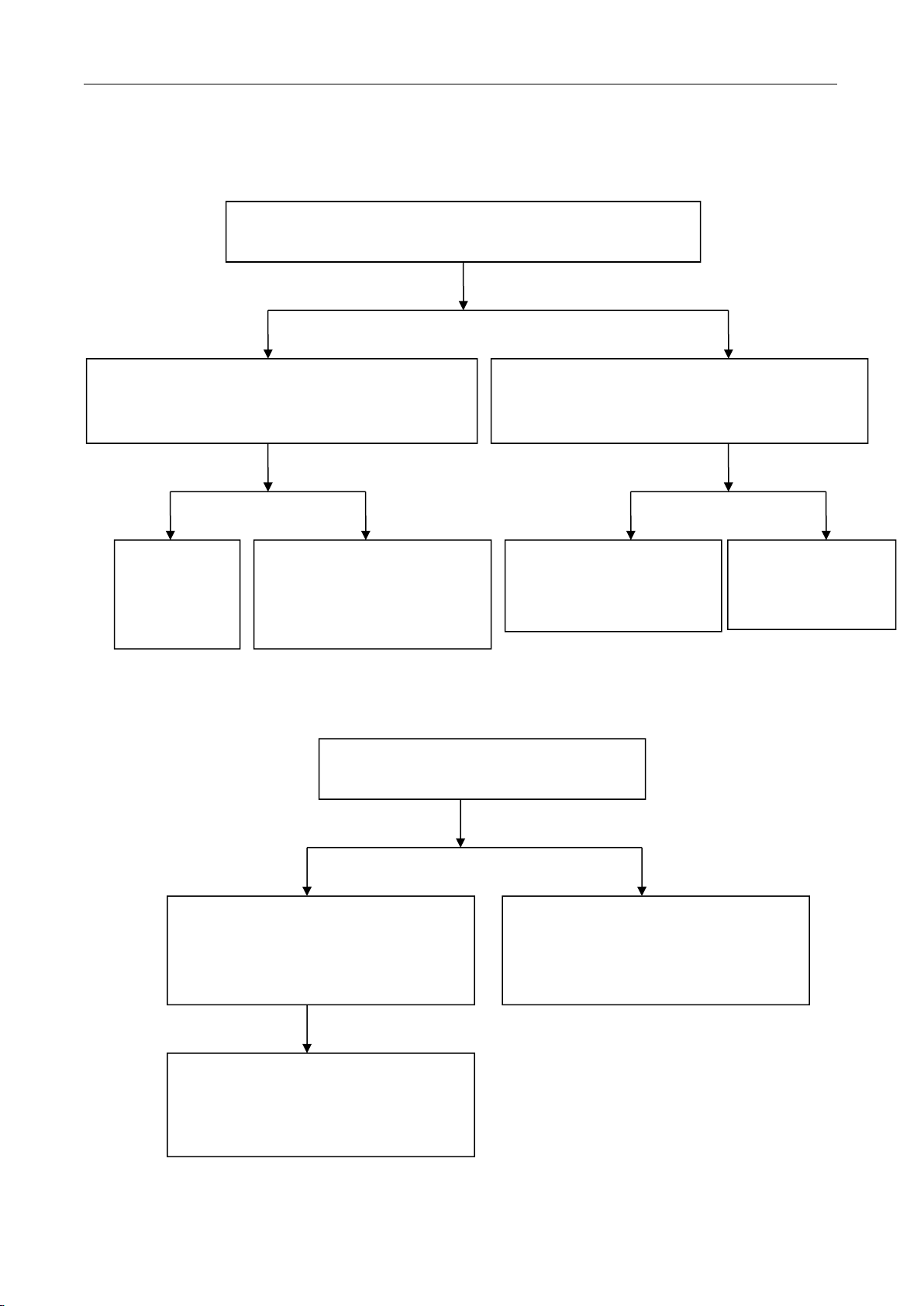
5. White screen after power-off (work normally when power on, but when power-off or
no signal input, the screen shows a white screen)
6. TV without channel or with color cast
Check whether there is change of voltage at the high voltage
board controlled by main board when power-on and power-off
Check whether the voltage change of the control pins on
the plug interface of high voltage board is normal when
power-on and power-off
Check whether the voltage of the pin on main chip
controlling the working voltage of high voltage board is
normal when power-on and power-off
YES
NO
The circuit
related to
high voltage
board is poor
Check whether the lines
between main board and high
voltage board is in open-loop
or poor contact
Check relevant circuits of
high voltage board
controlled by main board
Replace poor main
chips or recopy
software
Check TV antenna plug for looseness and
poor contact
If with color cast, check the setting of
color system under menu; and change
of color system to see whether it is
normal (Usually set to automatic)
Replace antenna plug
Check the antenna and its signal
source, if no problems exist, replace
tuner or control chips with the same
model
NO
YES
YES
YES
NO
NO
54
Page 56
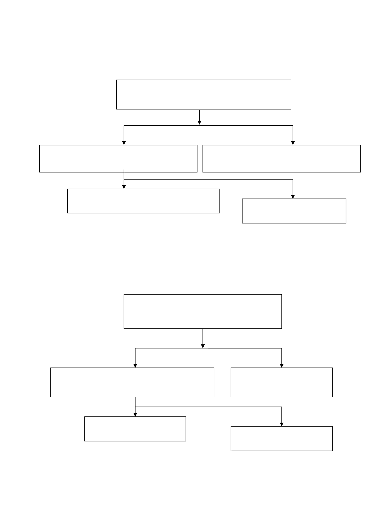
7. Poor sound
8. No VGA input signal
Switch to other audio input, check whether DVD
input and PC main board input has sound
Poor sound refers to without sound or with noise; check
whether the selection of sound system is proper
No sound; check whether remote control mute is
selected and switch sound system
No sound for other inputs; check the sound
amplifier and the shared control circuit
There is sound for other inputs,
replace TV tuner or control chip
YES
YES
NO
NO
VGA signal input does not respond, the screen
prompts “Please input signal”, check whether PC
signal source and signal line is normal.
Check VGA signal input board and see whether the row
and field sync signal protection diode is broke down
Replace PC or signal line, check
display VGA plug for looseness
Replace the motherboard or
factory reset is normal
Replace the 5.6V Zener diode
on the motherboard
NO
YES
YES
NO
55
Page 57
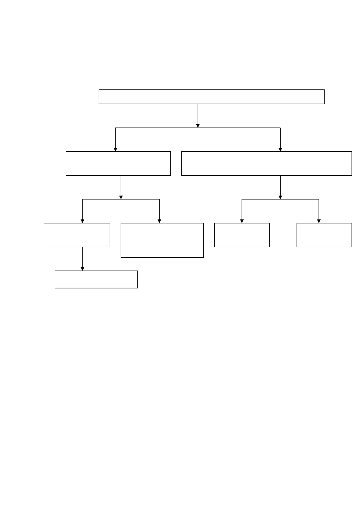
9. Poor embedded power supply of TV
10. Common fault of LCD screen
10.1 Bright line or bright belt (BL): constant longitudinal or transverse illuminating line or
belt due to non-conformed connection between IC and glass
10.2 Dark line (DL): constant longitudinal or transverse illuminating line due to
non-conformed connection between IC and glass.
10.3 White panel (WP): only light tube illuminates owing to non-conformed drive plate of
the LCD, without any display signal in the display area, and the whole screen is white.
10.4 Screen breaking: (overflow of LCD): with damage or invisible damage of the liquid
crystal glass, irregular black defect occurs from liquid crystal body to glass and polarizer,
which can not be seen at any image. The overflow portion can not form image and does not
display.
10.5 Pressing Scrape (PS): after local display area at the front of LCD is heavily pressed,
Power on, check embedded power supply 5VSB in TV for 5V voltage output
High electrical level existed at
STB (higher than 2.5V)
Replace power supply
YES
YES
NO
NO
Check EC2 for 380-400V
voltage; if there is not,
replace power supply
Check +5V , +12V
for normal input
YES
Check power supply line for looseness, check indictor for
working and power supply socket for looseness
NO
NO
Replace power
supply
Fasten lines
and socket
56
Page 58

glass of the pressed portion is not damaged, the liquid crystal body can not display normally,
with spot or block black defect.
10.6 Screen mess: irregular color display arising from damage of driving plate in LCD.
57
Page 59
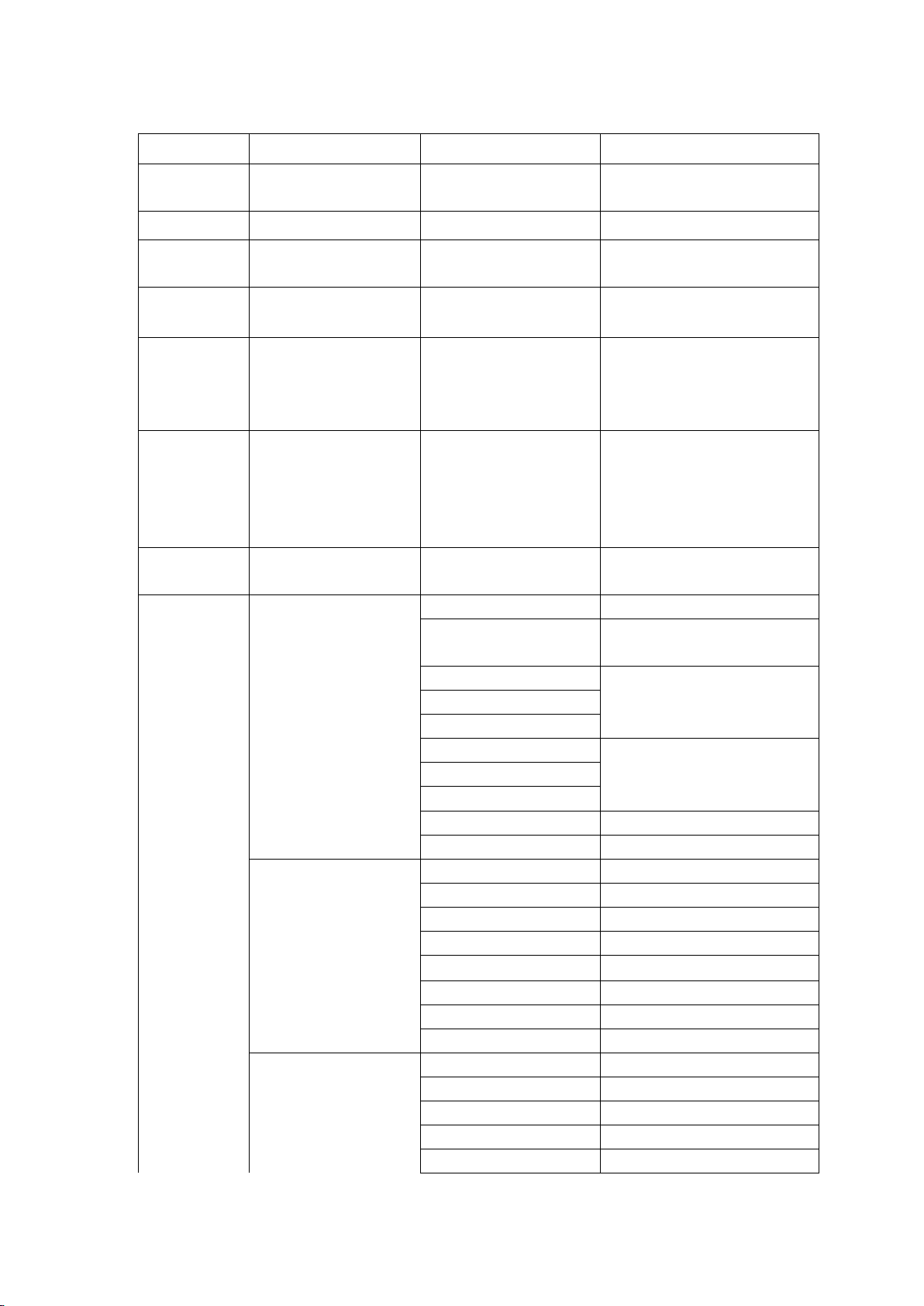
Enter into factory menu by signal source+left-right-left-right
Level 1 menu Level 2 menu Level 3 menu Value ,note
Factory reset
Aging mode
Preset
channel
power-up
mode
Mboot
upgrade
Main upgrade
Type in MAC
address
Data
debugging
Secondary/Memory/
Direct
Are you sure
Upgrade ?
选项:confirm/Cancel
Are you sure
Upgrade ?
Option:confirm and
Cancel
ADC ADJUST
White Balance
Picture Mode
Factory reset initialization
EEPROM Settings
Update Mboot
Update main procedure
ADC adjustment
Source
VGA(RGB),component(SD,H
D) choice
R-GAIN
The front-end gain adjustmentG-GAIN
B-GAIN
R-OFFSET
Clamp level adjustmentG-OFFSET
B-OFFSET
Phase phase
Auto Tune
Color temperature adjustment
Color Temperature
R Gain White level adjustment
G Gain
B Gain
R Offset Black level adjustment
G Offset
B offset
Image pattern adjustment
Brightness Brightness
Constrast Contrast
Saturation Saturation
Hue hue
58
Page 60
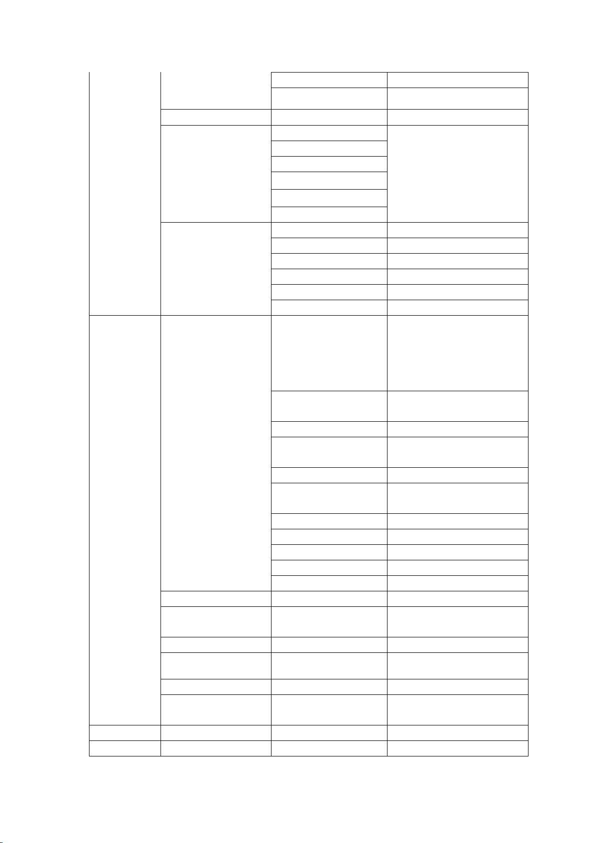
Test Pattern
Non_linear
OverScan
Sharpness Definition
Backlight Brightness
Various curve adjustmentOSD_0
OSD_25
OSD_50
OSD_75
OSD_100
Repetition rate adjustment
Source Various signal source
H size H adjustment
H position The center position of horizon
V size Field adjustment
V position The center position of field
PEQ adjustment;
Fo:Setting the center
frequency point of the gain
frequency band
Fo1 coarse
Range 0~16000,step is
100HZ
Fo1 fine Range 0~16000,step is 1HZ
PEQ
Fo2 coarse
Range 0~16000,step is
100HZ
Fo2 fine Range 0~16000,step is 1HZ
Fo3 coarse
Range 0~16000,step is
100HZ
Fo3 fine Range 0~16000,step is 1HZ
Fo4 coarse
Fo4 fine
Fo5 coarse
Fo5 fine
Uart Enable (switch Uart)On/off
Uart Debug
Debug tool can be used to read
COM port
EfficiencyBk
EfficiencyBk_Max
AVC
CEC/ARC
Other
Screen model
59
Page 61

PQ
Software
version
Barcode code
60
Page 62
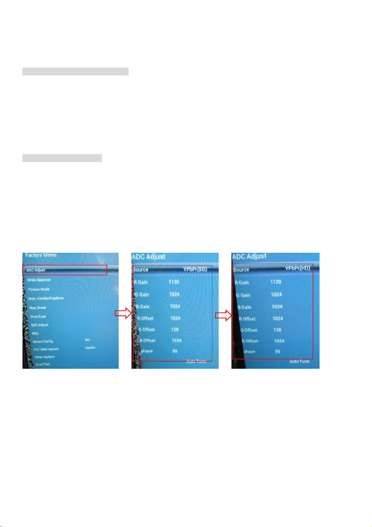
Net Work TV MSD6A628 software upgrading (After service)
1, software upgrade tools and materials
* PC (WINDOWS XP system, USB2.0)
* AC100 ~ 240V power supply and power cord
* ISP programming board and cable
* ISP programming board driver
* USB flash drive (version 2.0, the capacity is not more than 2G)
* Upgrade software and boot files
2, preparation before upgrade.
Write down all signal ADC and white balance data in factory menu before upgrading (FLASH initialization may occur
after upgrade, color calibration data erased, and then revert to the written down data):
1. Under YPbPb signal source, press the MENU key to pop up the main menu, and then press 8202 by number keys to
enter the factory menu, select ADC ADJUST item, press the OK button to enter the next menu, move the cursor to the
MODE key, press the left / right cursor keys to select YPbPr (SD) items, recorded R-GAIN / G-GAIN / B-GAIN value
and R-OFFSET / G-OFFSET / B-OFFSET value.
2. Undert ADC ADJUST item and press OK to enter the next menu move the cursor to the MODE key, press the left /
right keys to move the cursor to select YPbPr (HD) items, recorded R-GAIN / G-GAIN / B- GAIN value and R-OFFSET
/ G-OFFSET / B-OFFSET value.
3. Under VGA signal source, press MENU in the main menu pops up, then press 8202 by number keys to enter the
factory menu, select ADC ADJUST item and press OK to enter the next menu, move the cursor to the MODE key, press
the left / right cursor keys to select YPbPr (SD) items, recorded R-GAIN / G-GAIN / B-GAIN value and R-OFFSET /
G-OFFSET / B-OFFSET value.
61
Page 63
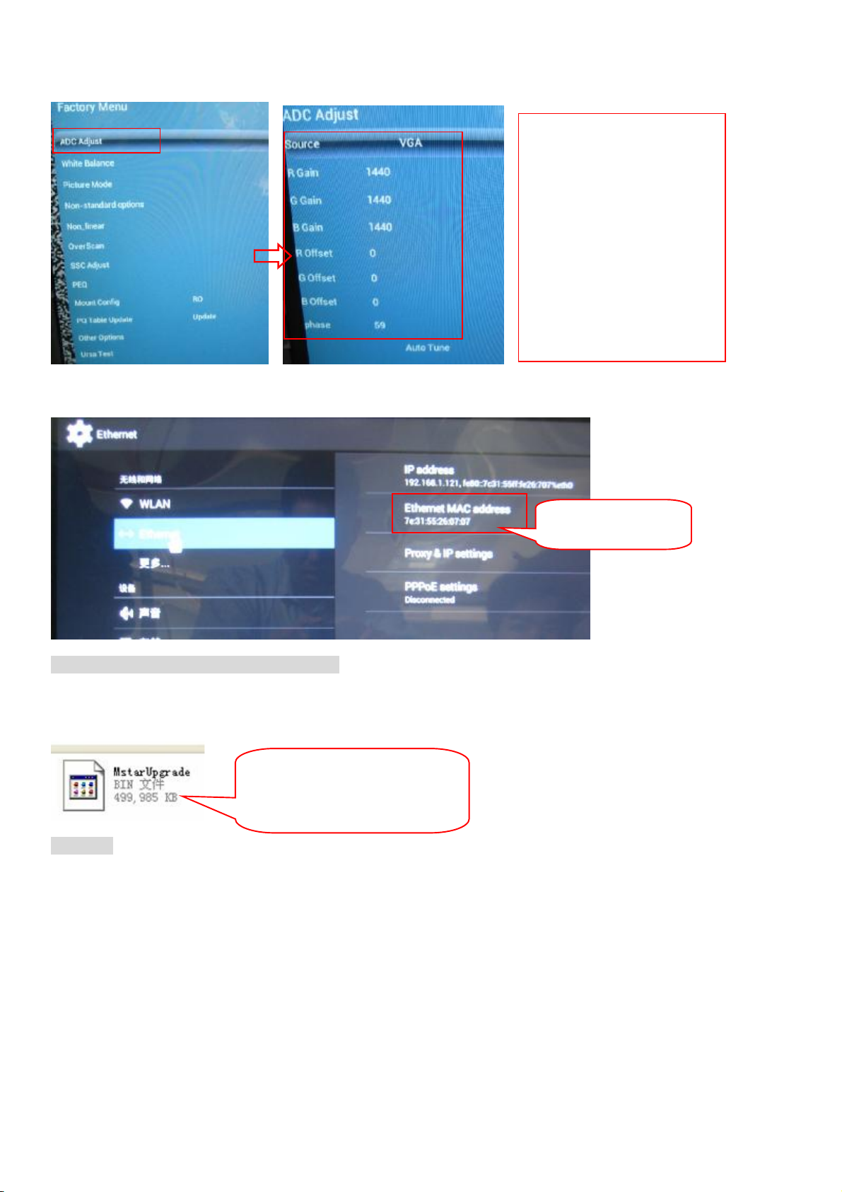
Wite donw YPbPr(SD)an
d
YPbPr(HD)value before upgrade
and wite down VGA mode
R/G/B-GAIN and R/B/G-OFFSET
value , change back to original
value after software upgrade
finished .
1. In Android system main interface, move cursor to “network”--“Ethernet”item, click mouse left button to get into ,
record MAC address.
MAC address
3, the software upgrade content and procedures :
1. U disk formatted as FAT32 format , and then upgrade the software ( software name and case is MstarUpgrade, suffix
bin) put in the U disk .
There are two ways for software upgrade, recommended mode 1.
The bigger the file, the longer time
upgrade will take, it is normally about
3~4 minutes,give enough time to
make sure upgrade success
Method 1: In the case of TV normally boot, enter the factory menu upgrade: power on machine, insert disk into the TV
USB interface, and then enter the factory menu, move the cursor to the Other Option Press OK to enter , and then move
the cursor to Upgrade Main options , press OK to upgrade.
62
Page 64
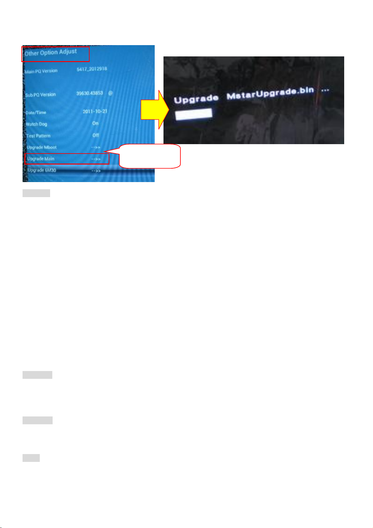
Press OK button to
upgrade
TV display tip
Method 2: Insert U disk into TV main board or programming fixture board USB interface , long press VOL + key, then
power on TV ( main board ) , after about five seconds the TV ( remote control panel ) indicator fast when flashing ,
indicating that the TV is being upgraded , after the light is not blinking on and off ( this process is time-consuming
depending on the size of the main board software , the greater the file the longer the software upgrade , the upgrade takes
roughly three minutes when the board software has 270M , 500M needs four minutes ) , means upgrade is complete .
3. Notes:
a. the file name and the case cannot be wrong , otherwise it will not be upgraded .
b. When using the U disk upgrade, sometimes light will no longer flashing after a TV remote control panel lights
flickering flashes ten seconds, this is upgrade failure. Normal upgrade remote panel lights flashing to be more than two
minutes, in this case upgrade again by powering off main board.
c. after powering off, if main board cannot upgrade normally , programming again the boot file (Mboot.bin or
MbootUprade.bin).
e. If the operator of this program is not familiar with the software, under the condition the can see factory menu
recommended upgrading the operating menu to enter the factory to prevent misuse.
4, when the above third step cannot be upgraded, upgrade the boot file first; please refer to the following specific
operating instructions.
MSD6A628 Network TV main board related upgrade packages with mboot.bin and MbootUpgrade.bin equipped with
two boot files. Both boot files function are the same, but there are differences between upgrade methods, only one
upgrade one of them. If the current TV main board can work properly, copy the boot files to the U disk after formatted
FAT32, then follow the instructions below to upgrade:
Method 1 : first MbootUpgrade.bin boot files, stored in the U disk, and then insert U disk in TV main board USB port,
press and hold the VOL + button on the TV control panel and hold, then power on TV ( main board), approximately after
five seconds the TV ( remote control panel ) indicator flashes rapidly , indicating that the TV is being upgraded , after the
light is not blinking on and off (time-consuming of this process approximately 60 seconds ) , indicating that the upgrade
is complete .
Method 2 : first Mboot.bin boot files stored in the U disk, then U disk inserted in the TV main board USB interface to
power on TV, and then press the MENU button on the remote control and then followed by 8202 the number keys to enter
the factory menu, move cursor to Other Option press OK to enter , and then move the cursor to upgrade mboot option ,
press OK to upgrade ( this time-consuming of this process is about 15 seconds ) .
Notes:
1.mboot.bin and MbootUpgrade.bin files can be put together in a U- disk, but no matter what methods to upgrade, all
operating according to operation instructions, control time to upgrade, ensure that the upgrade completed before power
failure, otherwise upgrade fails.
2. Because the boot files related to the TV's screen resolution and other relevant parameters, so before the software
63
Page 65
upgrade boot files of each board must be upgrade first.
3. If the above two methods cannot upgrade, using programming board online upgrade following the instructions:
5, Programming board driver installation.
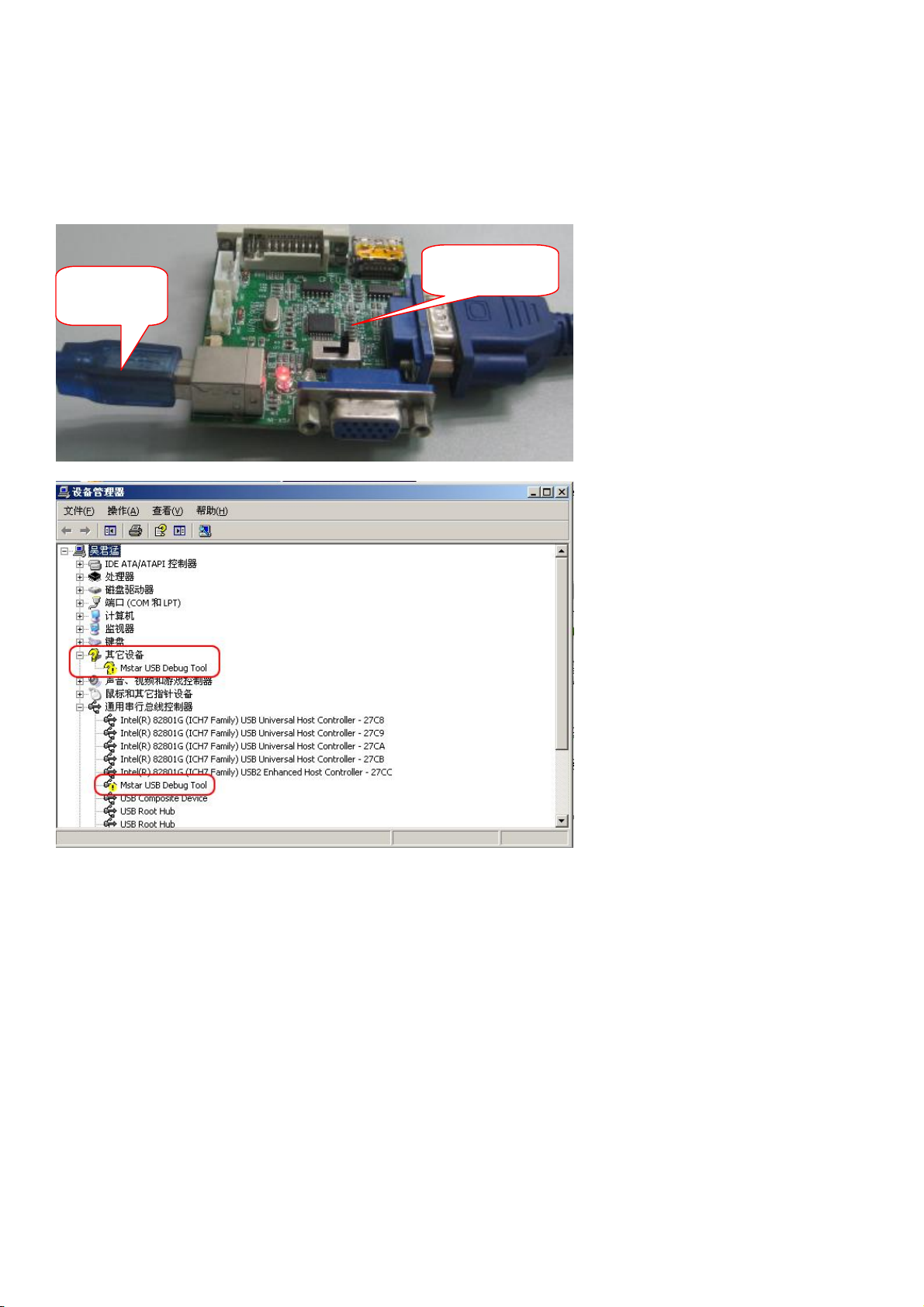
Use programming board online upgrade, programming board driver program has to be installed to PC, see the following
operation instructions.
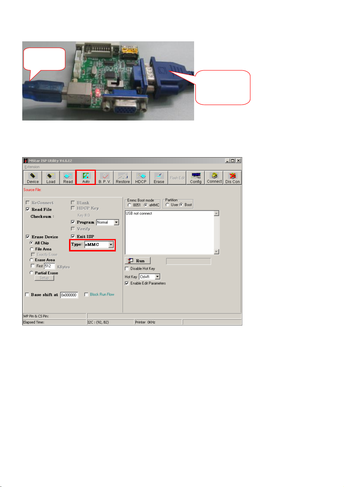
1.use USB connecting wire to connect programming board and personal PC.
ISP programming
To personal
board
PC
2. PC identify new device, choose to install from list or specified location and appoint driver file position as figure.
64
Page 66
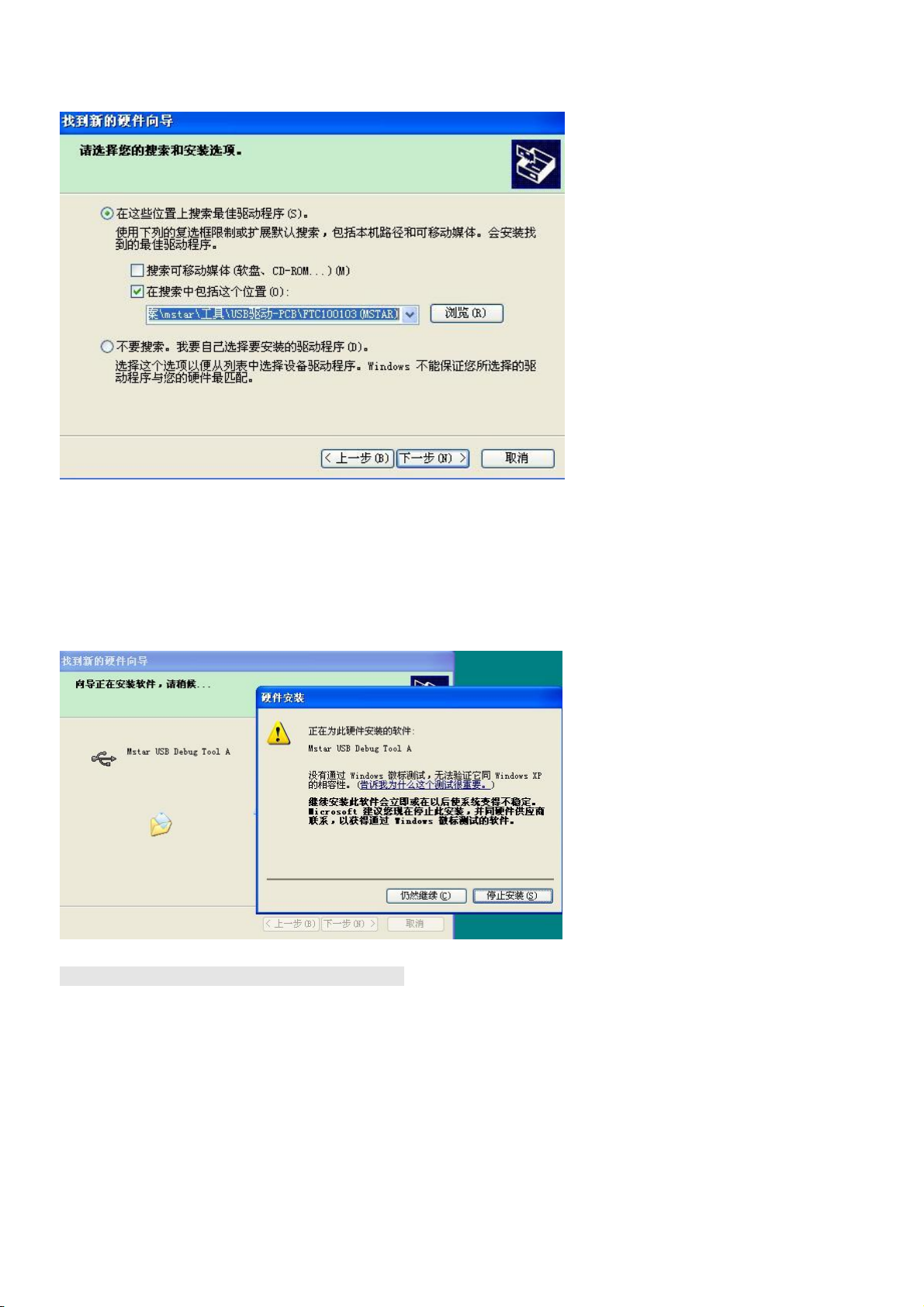
3. after PC finds driver file, below information will be prompted during installation, click on , remains can be installed, the
system will install the driver process three times , namely : Mstar USB Debug Tool A; Mstar USB Debug Tool B; Mstar
USB SerialPort , install the three drives in order !
6. use programming board online upgrade boot file.
1. Use a USB cable and VGA cable to connect the programming board and TV main board , computer main bard and
then powering on main board.
65
Page 67
To personal PC
USB interface
To TV main
board VGA
socket
2. Double-click to run MStar ISP Utility v4.6.t2.exe, click the "Auto" icon on the main toolbar under the type selected for
eMMC.
3. Click the "Read" button in the main toolbar under load in EISP Loader File1 munim_EISP_boot _ ** _ **. Bin, in EISP
Read File1 load rom_emmc_boot.bin, in EISP Loader File2 load munim_EISP_user _ ** _ **. Bin, load mboot.bin
( Figure 2 ) in EISP Read File2.
66
Page 68
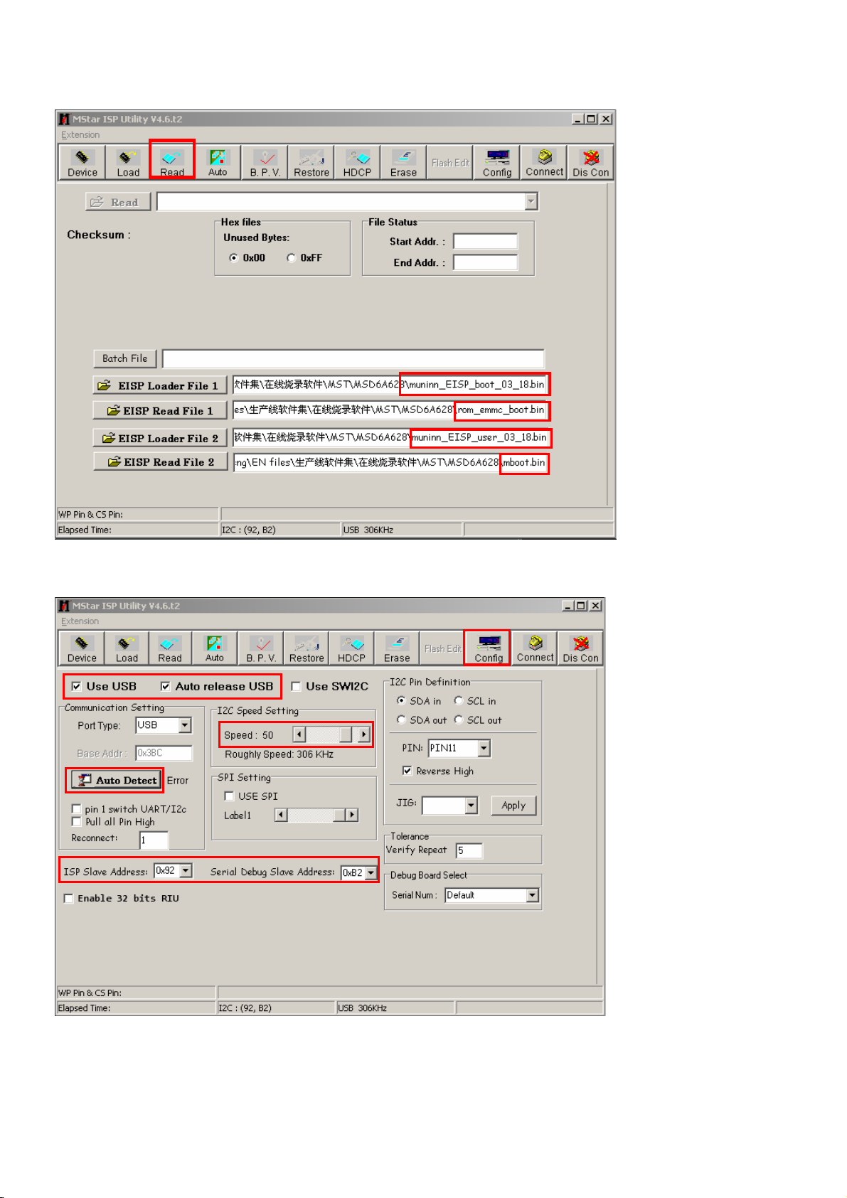
4. Click on the main toolbar "Config" button , the interface is set up according to the pictures of their respective settings.
5. Click on the main toolbar "Connet" button at the top of the tab bar to run the program will display [ Device Type
eMMC ] .
67
Page 69
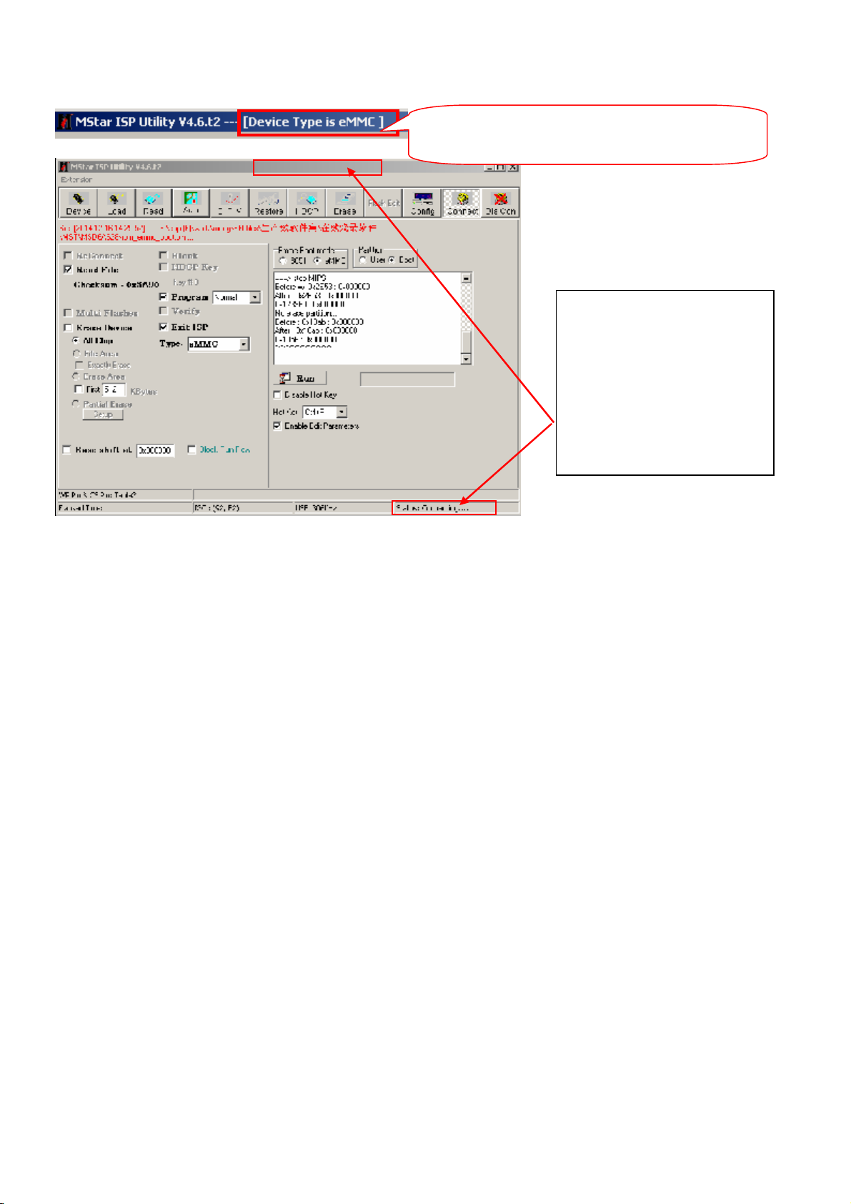
Click “Connet” button under tool bar, running
program top part will show【Device Type eMMC】
After click“Stop/Run”button,
if interface lower right corner
shows “Connecting.....” and tab
bar shows as “【 Device Type
eMMC】 “ means connecting is
failed or current main board can
only us U disk to upgrade.
If there is no showing of [ Device Type eMMC ] upgrade cannot be conducted , please check the programming board is
properly connected and if main board can boot (main board can boot normally not display [ Device Type eMMC ,] need to
upgrade the software, copying it into U disk, press and hold the button panel VOL + button first and powering on main
board, wait for LED indicator on the machine flashes for about five seconds and then unplug the U disk and re- power
main board to display ) .
7. Check "Auto" icon in the menu settings are consistent with the figure below, and then click "Run" button to boot file to
program.
68
Page 70
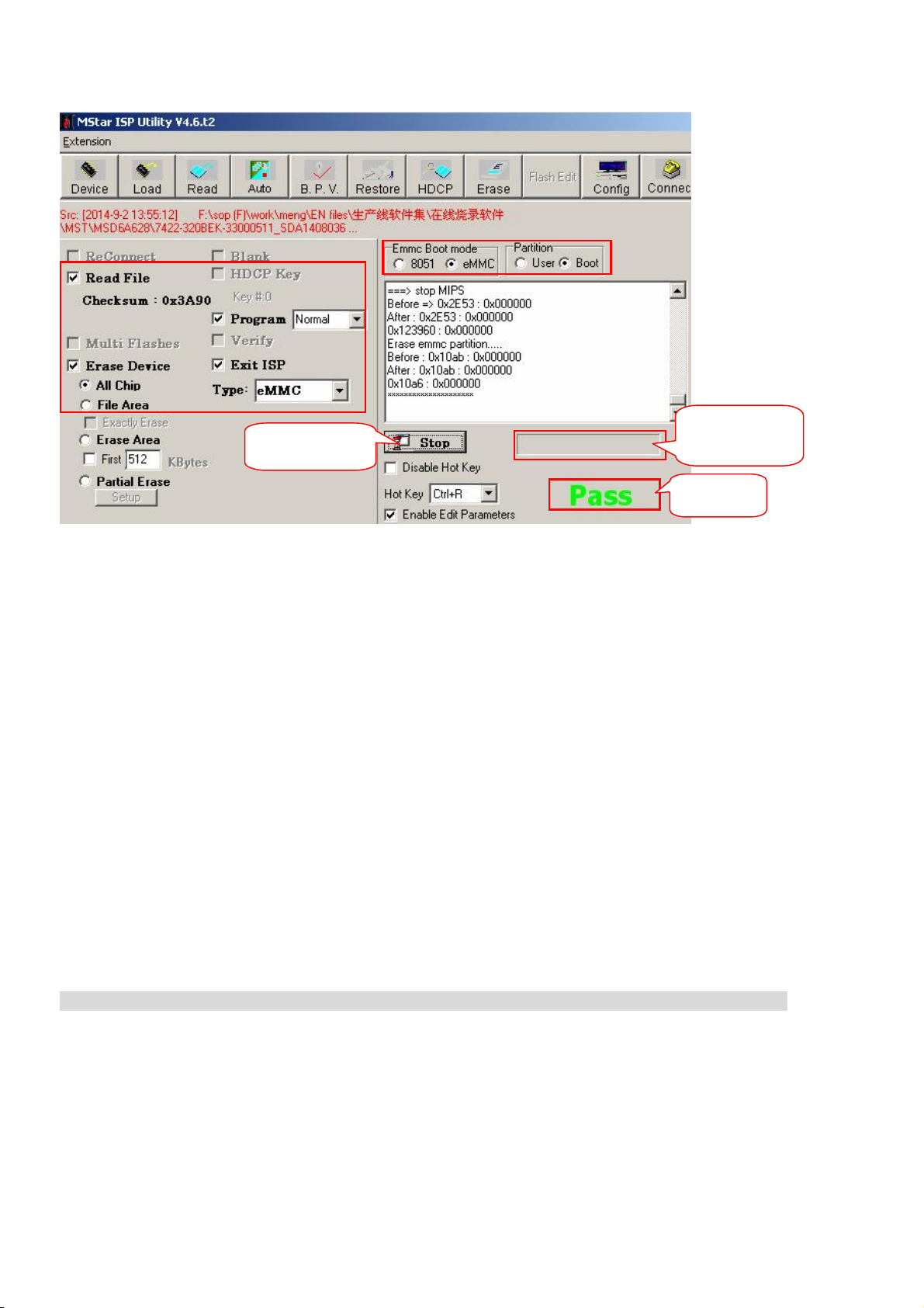
Programming
prog
Execute button
ress
result
Programming progress bar will scroll now, after programming is finished, it will show “Pass”。
7, Main board driver upgrade.
1. U disk formatted as FAT32 format, and then upgrade the software ( software name is MstarUpgrade, suffix is bin) put in
U disk .
2. Insert U disk into main board or programming TV fixture USB port , press VOL + key, then power on TV ( main board)
after about five seconds the TV ( remote control panel ) indicator flashes rapidly , indicating the TV is being upgraded ,
when the light stops blinking and goes out ( this process time-consuming is depending on the size of the main board
software , the greater the file the longer the software upgrade time , when the board is 270M, upgrade software takes
roughly three minutes ,when 500M , it is about four minutes ) , indicating that the upgrade is complete .
3. Notes:
a. the file name and case cannot be wrong , otherwise it will not be upgraded .
b. When using U disk to upgrade, sometimes after light does not flat after a TV remote control panel lights flickering
flashes ten seconds, this is upgrade failure. Normal upgrade remote panel lights flashing more than two minutes , place the
board in case of power failure in this case re- board software upgrade.
c.main board cannot be upgraded after powering on , please programming boot file again (Mboot.bin or
MbootUprade.bin).
8, after the upgrade is complete, install machine cover, before delivery, factory adjustment must be carried out :
1. powering on machine, press the MENU button on the remote control to the main menu pops up, then press 8202
followed by the number key to enter the factory menu , press the up / down keys to move the cursor to the "Other Options"
option Press the Up / Down keys move the cursor to the "Restore To Default" option by right the reset command , a black
screen for about 8 seconds and the machine automatically re- power on reset operation is completed .
Page 71
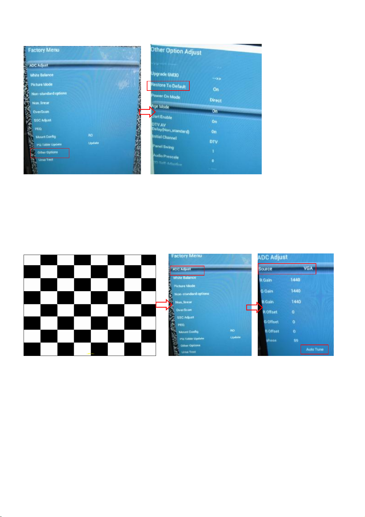
2. Completed initialization within three minutes after inserting VGA signal wire and powering on machine (automatically
initializes started after factory menu reset is ) switch to VGA signal source . Press the MENU key to pop up the main menu, and
then followed by 8202 the number keys to enter the factory menu, press the Shift key to "ADC ADJUST" and press the OK
button to enter the next menu, press the left / right keys to move the cursor to select VGA item, then press shift keys to move the
cursor to the AUTO TUNE key and press the OK button to execute the self-adjusting command. There is a corresponding entry in
the AUTO TUNE Tip: SUCCESS, means self-adjusting qualified, FAILS, means self-tuning failure, need to self adjusting again.
3. under YPbPb source ,input 480i 100% color bar signal to machine . after press NEMU poping-up main menu , then
followed by 8202 the number keys to enter the factory menu , select ADC ADJUST item , press the OK button to enter the
next menu , press the left / right keys to move the cursor to select YPbPr (SD) item , press down keys to move the cursor to
the AUTO TUNE key and press the OK button to execute the self-adjusting color commands. There is a corresponding
entry in the AUTO TUNE Tip : SUCCESS , means self-adjusting qualified , FAIL , means self-adjusting is filed, needed to
adjust again.
70
Page 72
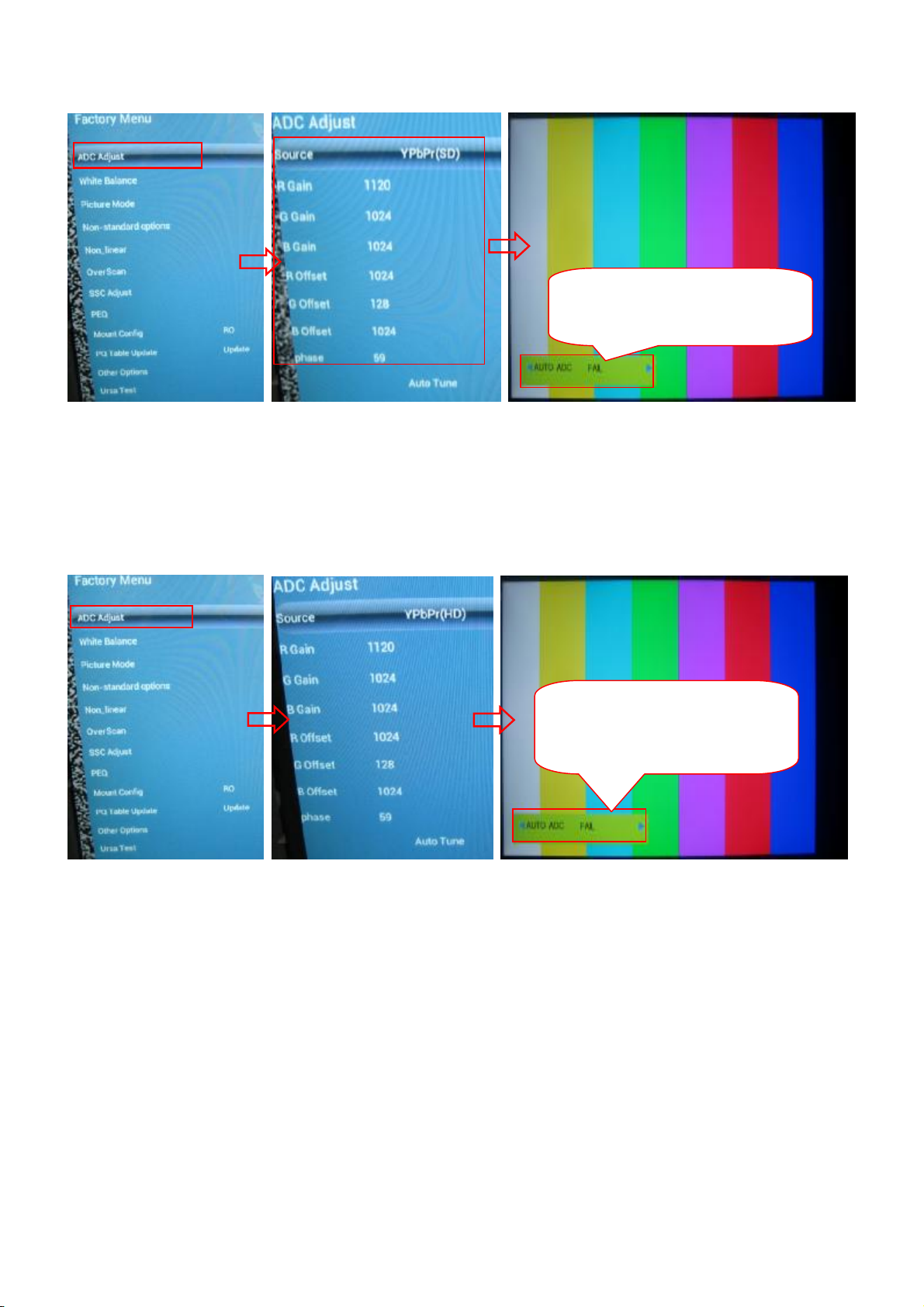
Press right and left key to execute se
lf
lf
L
adjusting order , SUCCESS is OK ,FAIL
is failure ( need to re adjusting)
4. Under YPbPb signal source , input 720P 100% color bar signal to machine. Afater pressing NEMU pop-up main menu,
then followed by 8202 the number keys to enter the factory menu , select ADC ADJUST item , press the OK button to
enter the next menu , press the left / right keys to move the cursor to select YPbPr (HD) key, then press down keys to move
the cursor to the AUTO TUNE key and press the OK button to execute the self-adjusting color commands. There is a
corresponding entry in the AUTO TUNE Tip : SUCCESS , means self-adjusting qualified , FAIL , means self adjusting is
failed, need to adjust again.
Press right and left key to execute se
adjusting order , SUCCESS is OK ,FAI
is failure ( need to re adjusting)
5. about white balance adjustment:
* need to input standard graphics to TV during auto white balance self adjusting, recommended instrument is
CHROMA222293.
* In case not plugging signal line, in the factory menu of ADC Adjust, change the source value of VGA, YPBPR (HD),
R-GAIN YPBPR (SD) for each mode / G-GAIN / B -GAIN value and R-OFFSET / G-OFFSET / B-OFFSET to the
original value before upgrade.
9 , MAC address programming refers to "MSD6A628 Msd6a608 MSD6A818 smart network TV MAC address code
programming Guide" , in general, just use U disk to upgrade ( do not use programming board burn boot files MAC in
machine, will not erased , if using programming board to re- burn the boot files , MAC address programming is
needed ) .
10, after ADC ADJUST debugging finished, press the MENU button several times to exit the factory menu to save the
data , turn the machine off and then restore the original packaging.
71
Page 73
5
4
3
2
1
MSD6A628
PAGE
D D
1 Index&History Rev
2
3
4
方案
--T8E
Block Diagram
System Power
MSD6A628
大板原理图
Content
VER:A1.0 2014-8-12
MSD6A628 POWER5
6
7
8
C C
LVDS &Tuner &NAND page
Video&VGA&USB&Amplify page
HDMI&Ethernet page
History Rev
Author
ZHQINGFirst Version Release
Ver:A1.06/25/2014
Rev
DescriptionDATE
B B
A A
本文档仅限中国深圳市康冠技术有限公司和被呈送方内部使用,未经书面许可请勿扩散到第三方。
This document for ShenZhen KTC Technology CO., Ltd and presented party internal use only,
Do not spread to third party without the written permission.
版权所有@深圳市康冠技术有限公司
5
4
Copyright@ ShenZhen KTC Technology Co., LTD
3
文件名称:
文件名称:
文件名称:
文件编号:
文件编号:
文件编号:
设计:
设计:
设计:
发行部门: 生效日期:
发行部门: 生效日期:
发行部门: 生效日期:
2
KTC ISO9001.ISO14001体系文件
KTC ISO9001.ISO14001体系文件
KTC ISO9001.ISO14001体系文件
MSD6A628方案T8大板DTMB数模一体智能电视原理图
MSD6A628方案T8大板DTMB数模一体智能电视原理图
MSD6A628方案T8大板DTMB数模一体智能电视原理图
T4251
张志清
张志清
张志清
研发处
研发处
研发处
版本:3.0
版本:3.0
版本:3.0
审核:
审核:
审核:
页数:
页数:
页数:
批准:
批准:
批准:
Friday, August 15, 2014
Friday, August 15, 2014
Friday, August 15, 2014
1
18
18
18
of
of
of
72
Page 74
5
4
3
2
1
3.3V_NORMAL
GPIO
AS1117
1.28V
DC-DC
1.15V
DC-DC
TUNER_3.3V
TUNER PWR
AS1117
DDR PWR
DC-DC
3.3V_STANDBY
AS1117
32Gbit
EMMC FLASH
HDMI1
(ARC)
HDMI2
HDMI3
(MHL)
VDDC_CPU PWR
VDDC PWR
DDR PWR 1.5V
3.3V_Standby
HDMI1
HDMI2
LAN
屏电压
12V_NORMAL
MOS
MSD6A628
LAN
Y/Pb/Pr
管控制
Y/Pb/Pr
40P LVDS
AV-IN
VGA
COAXIAL
VGA
RESET
D D
12V_NORMAL
5V_NORMAL
5V_STANDBY
PWR_ON/OFF
三极管控制
C C
USB
AV-OUT
COAXIAL
12V_NORMAL
Audio AMP
TPA3110LD2
IF
TUNER_3.3V
IR&KEY
VEDIO-OUT
SPK-L
SPK-R
SILICON TUNER
TDA18275HN
IR&KEY
TUNER CONN
USBAV-IN
RF
B B
A A
文件名称:
文件名称:
文件名称:
文件编号:
文件编号:
本文档仅限中国深圳市康冠技术有限公司和被呈送方内部使用,未经书面许可请勿扩散到第三方。
This document for ShenZhen KTC Technology CO., Ltd and presented party internal use only,
Do not spread to third party without the written permission.
5
4
3
版权所有@深圳市康冠技术有限公司
Copyright@ ShenZhen KTC Technology Co., LTD
文件编号:
设计:
设计:
设计:
发行部门: 生效日期:
发行部门: 生效日期:
发行部门: 生效日期:
2
KTC ISO9001.ISO14001体系文件
KTC ISO9001.ISO14001体系文件
KTC ISO9001.ISO14001体系文件
MSD6A628方案T8大板DTMB数模一体智能电视原理图
MSD6A628方案T8大板DTMB数模一体智能电视原理图
MSD6A628方案T8大板DTMB数模一体智能电视原理图
T4251
张志清
张志清
张志清
研发处
研发处
研发处
版本:3.0
版本:3.0
版本:3.0
审核:
审核:
审核:
页数:
页数:
页数:
批准:
批准:
批准:
Friday, August 15, 2014
Friday, August 15, 2014
Friday, August 15, 2014
1
28
28
28
of
of
of
73
Page 75
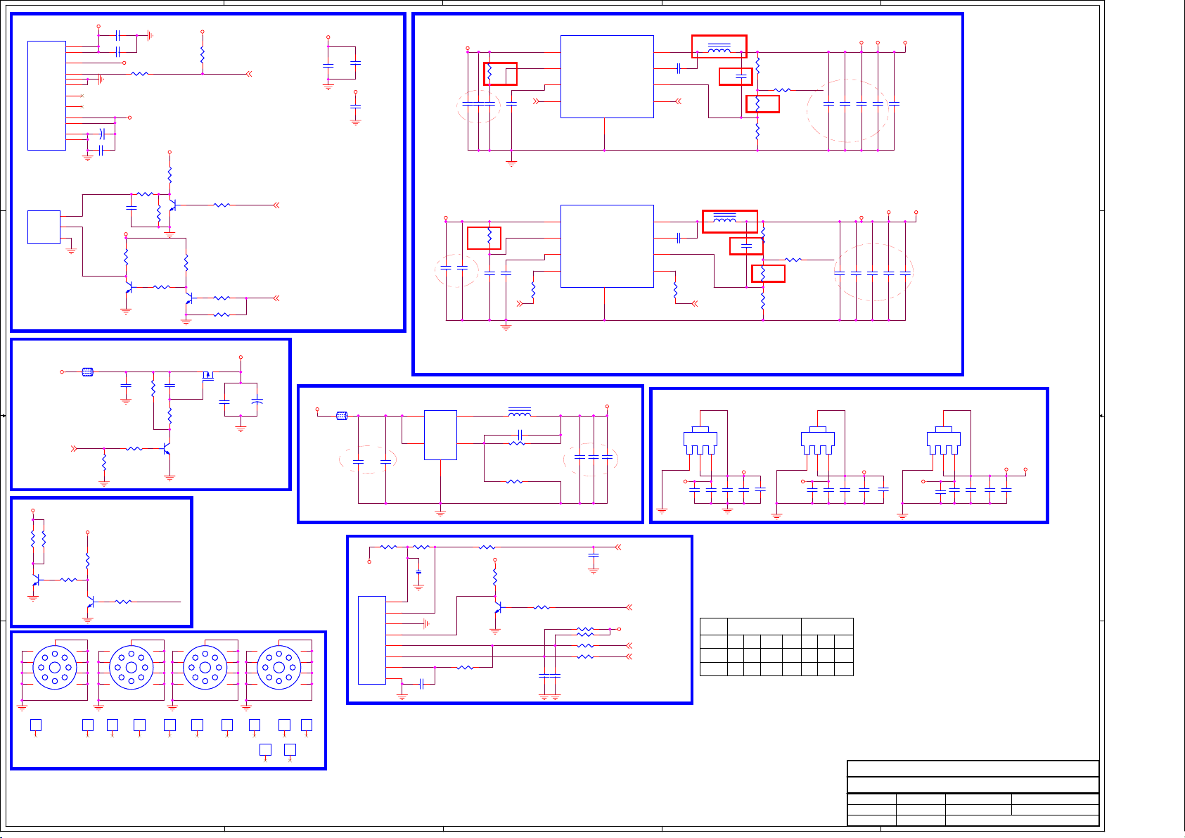
5
PM5V
PM5V
5VSB
standby
GND
GND
12V
12V
GND
GND
+5V_Normal
1
2
3
STANDBY
4
5
6
7
8
9
10
C138 470uF/16VC138 470uF/16V
11
12
C139 0.1uFC139 0.1uF
C143 10uFC143 10uF
C140 0.1uFC140 0.1uF
+5V_Standby
R14 100RR14 100R
+12V_NORMAL
Connetor
CN101 12pin/2.0MMCN101 12pin/2.0MM
BL_ON/OFF
BL_PWM
D D
Inverter controler
BL-ADJUST
1
BL_ADJUST
2
BL_ON/OFF
3
GND
CN102
CN102
3Pin/2.0MM
3Pin/2.0MM
BL-ON/OFF
C C
C53
C53
2.2uF/DC
2.2uF/DC
+5V_Normal
R52
R52
4.7K
4.7K
R511K R511K
R49
R49
NC/10K
NC/10K
Q10
Q10
R57 4.7KR57 4.7K
1
3904
3904
2 3
Power for panel
+12V_NORMAL
+12V_Normal
B B
Q208
Q208
3904
3904
PANEL_ON/OFF4
2 3
5
4
3
2
R3200R R3200R
R15200R R15200R
R13 10KR13 10K
1
H12NCH12
NC
1
L111
L111
PANEL_ON/OFF
Q207
Q207
3904
3904
9
8
7
6
0805_BEAD/12V
0805_BEAD/12V
+3.3V_Standby
R9
10KR910K
R12 10KR12 10K
1
2 3
屏
屏
R42 4.7KR42 4.7K
R40
R40
10K
10K
H11NCH11
5
4
3
2
C37
C37
0.1uF
0.1uF
NC
R41
R41
10K
10K
STANDBY
12V
1
9
8
7
6
+5V_Standby
H:ON
L:OFF
+5V_Normal
R61KR6
1K
Q1
1
3904Q13904
2 3
SAMSUNG panel 0~3.3V R34=10K
LG/CMO/AU panel 0~5V,R34 NC
R43
R43
10K
10K
Q11
Q11
3904
3904
2 3
VCC_P
C67
C67
1uF
1uF
PANEL_ON
R58
R58
100K
100K
Q9
1
3904Q93904
2 3
放电电路
H21NCH21
5
4
3
2
NC
R46
R46
4.7K
4.7K
PWR-ON/OFF
R54 4.7KR54 4.7K
1
R53 10KR53 10K
Q12
Q12
ME2325
ME2325
1
R504.7K R504.7K
Panel_VCC
C47
C47
0.1uF
0.1uF
9
8
7
6
PWR-ON/OFF 4
BRI_ADJ 4,6
VBL_CTRL 4
"VBL_CTRL" IO
"VBL_CTRL" IO
CA8
CA8
+
+
100uF/16V
100uF/16V
H22NCH22
1
5
4
3
2
NC
+5V_Standby
口为高电平时,背光开。
口为低电平时,背光关。
+5V_Standby
靠近
9
8
7
6
4
C141
C141
C137
C137
10uF
10uF
0.1uF
0.1uF
+5V_Normal
L112 0805_BEADL112 0805_BEAD
C114
C114
10uF
10uF
DC-DC
+5V_Standby
8pin/2.0MM
8pin/2.0MM
CN103
CN103
C144
C144
10uF
10uF
+5V_IN
R168 10RR168 10R
IR_IN
GND
LED
KEY0
KEY1
PWR
GND
VDDC DC/DC
+5V_Normal
C128
C128
10uF
10uF
靠近
电阻靠近
U12
U12
SY8088
SY8088
4
SW3VIN
1
EN
R157
R157
10K
10K
0.1uF
0.1uF
C181
C181
IR_5V
IR-in
LED+
KEY0-in
KEY1-in
C174 0.1uFC174 0.1uF
FB
GND
2
IR-in
R194 1KR194 1K
C106
C106
0.1uF
0.1uF
1
2
3
4
5
6
7
8
KEY_POWER
3
+5V_Normal
R123
R123
100K
100K
C103
C103
C113
C113
C134
C134
C111
C111
M_SDA4 M_SCL 4
1uF
1uF
0.1uF
0.1uF
10uF
10uF
10uF
10uF
靠近
DC-DC
!!!
R121
R121
100K
100K
C122
C122
C130
C130
C131
C131
10uF
10uF
0.1uF
0.1uF
1uF
1uF
R122
DC-DC
DCDC,
敏感线,远离干扰源
至少需使用
5
Vout=0.6V*(1+R1/R2)
R167 100RR167 100R
+5V_Standby
Q112
Q112
3904
3904
R122
100R
100R
!!!
L12
L12
SWPA3015S2R2NT/1.5A
SWPA3015S2R2NT/1.5A
C110 33pFC110 33pF
R103 3KR103 3K
R1
R111 2KR111 2K
R2
R1822KR182
2K
R126 4.7KR126 4.7K
1
2 3
C179
C179
0.1uF
0.1uF
500mA DC/DC!!
12
U15
U15
8
PVDD
1
EN
3
5V
4
SDA
PowerPAD
9
至少需使用
U14
U14
8
PVDD
1
EN
3
5V
4
SDA
PowerPAD
9
Addr 0xC0
至少需使用
+1.5V_DDR
1A Max
C117
C117
C118
C118
C105
C105
0.1uF
0.1uF
22uF
22uF
10uF
10uF
靠近
DC-DC
IRIN
C148
C148
33pF
33pF
LED
R159 4.7KR159 4.7K
R155 4.7KR155 4.7K
R171 1KR171 1K
R142 1KR142 1K
C150
C150
0.1uF
0.1uF
IR&KEY Connector
6
LX
C125 0.1uFC125 0.1uF
7
BST
2
FB
5
SCL
MSH6000A1
MSH6000A1
Addr 0xC2
Vout=1.1V*(1+R1/R2)
5A的 DC/DC
6
LX
C121 0.1uFC121 0.1uF
7
BST
2
FB
5
SCL
R124
R124
100R
MSH6000A
MSH6000A
2A的 DC/DC
100R
Vout=1.1V*(1+R1/R2)
LDO
IRIN 4
LED 4
+3.3V_Standby
KEY_SAR0 4
KEY_SAR1 4
L11
L11
SWPA8040S2R2NT/5A
SWPA8040S2R2NT/5A
FB1
3R3/2A
3R3/2A
FB2
M_SCL 4M_SDA4
4
U11
U11
ADJ
OUT
ADJ
OUT
IN
IN
321
C109
C109
C135
C135
2.2uF
2.2uF
0.1uF
0.1uF
所用IO口
按键功能
电阻值
电压值
R1
R2
L13
L13
AMS1117L-3.3
AMS1117L-3.3
C101
C101
0.1uF
0.1uF
12
C120
C120
18nF
18nF
12
C126
C126
18nF
18nF
R104
R104
47K_1%
47K_1%
500mA
+3.3V_Standby
C102
C102
2.2uF
2.2uF
欧
0.98V0V 1.95V
2
R116
R116
NC/0R
NC/0R
VDDC_VSENSE
R117 0RR117 0R
R101
R101
2.7K_1%
2.7K_1%
R114
R114
47K_1%
47K_1%
开机初始电压保证到
R115
R115
NC/0R
NC/0R
R113 0RR113 0R
R102
R102
6.2K_1%
6.2K_1%
R1
R2
开机初始电压保证到
ADJ
ADJ
+5V_Normal+5V_Standby
C115
C115
10uF
10uF
SOURCECH-CH+
POWER
1K6.8K2K0
0.58V
C119
C119
22uF
22uF
22uF
22uF
靠近
VDDC_CPU_1.15V
VDDC_CPU_VSENSE
C133
C133
22uF
22uF
靠近
4
U13
U13
OUT
OUT
IN
IN
321
C123
C123
C107
C107
2.2uF
2.2uF
0.1uF
0.1uF
SAR1SAR0
MENUV0L+V0L-
6.8K2K0
欧
1.95V0.98V0V
VDDC
C124
C124
C127
C127
C132
C132
0.1uF
0.1uF
22uF
22uF
22uF/nc
22uF/nc
DC-DC
IC pin 为1.15V
VDDC_CPU
C104
C104
C145
C145
C129
C129
0.1uF
0.1uF
22uF
22uF
22uF
22uF
DC-DC
IC pin 为1.24V
AMS1117L-3.3
AMS1117L-3.3
400mA Max
+3.3V_Normal
C116
C116
C108
C108
C112
C112
0.1uF
0.1uF
2.2uF
2.2uF
10uF
10uF
VDDC_VSENSEVDDC_1.15V
C136
C136
!
VDDC_CPU_VSENSE
C146
C146
22uF/nc
22uF/nc
!
ADJ
OUT
ADJ
OUT
+5V_Normal
C78
C78
2.2uF
2.2uF
TUNER POWER
4
U16
U16
IN
IN
321
C48
C48
0.1uF
0.1uF
1
AMS1117L-3.3
AMS1117L-3.3
310mA Max
+3.3V_TU
C15
C15
C49
C49
0.1uF
0.1uF
2.2uF
2.2uF
V_TU
C50
C50
22uF
22uF
A A
1
H26NCH26
NC
1
1
H23NCH23
H24NCH24
NC
NC
1
1
1
H29NCH29
H20NCH20
NC
NC
1
H17NCH17
H19NCH19
NC
NC
Test Point & MARK
5
1
1
NC
1
H27NCH27
H28NCH28
1
NC
H30NCH30
NC
NC
1
SNNCSN
SN2NCSN2
NC
本文档仅限中国深圳市康冠技术有限公司和被呈送方内部使用,未经书面许可请勿扩散到第三方。
This document for ShenZhen KTC Technology CO., Ltd and presented party internal use only,
Do not spread to third party without the written permission.
4
3
版权所有
@
深圳市康冠技术有限公司
Copyright@ ShenZhen KTC Technology Co., LTD
2
文件名称:
文件名称:
文件名称:
文件编号:
文件编号:
文件编号:
设计:
设计:
设计:
发行部门: 生效日期:
发行部门: 生效日期:
发行部门: 生效日期:
KTC ISO9001.ISO14001体系文件
KTC ISO9001.ISO14001体系文件
KTC ISO9001.ISO14001体系文件
MSD6A628方案T8大板DTMB数模一体智能电视原理图
MSD6A628方案T8大板DTMB数模一体智能电视原理图
MSD6A628方案T8大板DTMB数模一体智能电视原理图
T4251
张志清
张志清
张志清
研发处
研发处
研发处
版本:3.0
版本:3.0
版本:3.0
审核:
审核:
审核:
页数:
页数:
页数:
批准:
批准:
批准:
Friday, August 15, 2014
Friday, August 15, 2014
Friday, August 15, 2014
1
of
of
of
38
38
38
74
Page 76
5
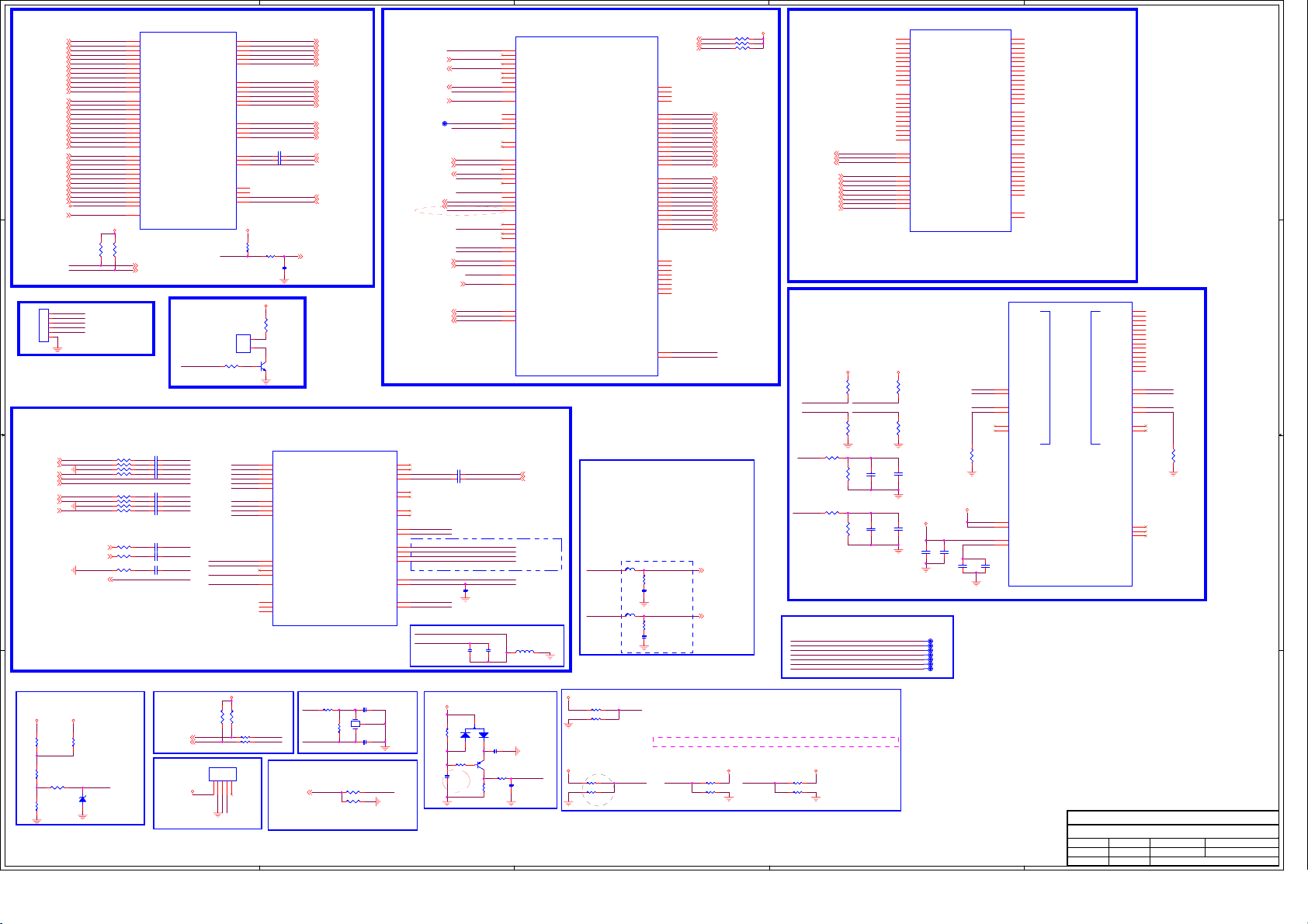
HDMI
HDMI Interface
HDMI1-RX0N
HDMI1-RX0N8
HDMI1-RX0P
HDMI1-RX0P8
HDMI1-RX1N
HDMI1-RX1N8
HDMI1-RX1P
HDMI1-RX1P8
HDMI1-RX2N
HDMI1-RX2N8
HDMI1-RX2P
HDMI1-RX2P8
HDMI1-CLKN
HDMI1-CLKN8
HDMI1-CLKP
HDMI1-CLKP8
HDMI1-SCL
HDMI1-SCL8
HDMI1-SDA
HDMI1-SDA8
HDMI1-HPDIN
HDMI1-HPDIN8
HDMI1-ARC
HDMI1-ARC8
HDMI2-RX0N
HDMI2-RX0N8
HDMI2-RX0P
HDMI2-RX0P8
HDMI2-RX1N
HDMI2-RX1N8
HDMI2-RX1P8
HDMI2-RX2N8
HDMI2-RX2P8
HDMI2-CLKN8
HDMI2-CLKP8
HDMI2-SCL8
HDMI2-SDA8
HDMI2-HPDIN8
HDMI3-RX0N8
HDMI3-RX0P8
HDMI3-RX1N8
HDMI3-RX1P8
HDMI3-RX2N8
HDMI3-RX2P8
HDMI3-CLKN8
HDMI3-CLKP8
HDMI3-SCL8
HDMI3-SDA8
HDMI3-HPDIN8
AVDD5V_MHL
J109
J109
1
2
3
4
5
6
NC/CON6-2.0
NC/CON6-2.0
HDMI-CEC8
3D_L/R_FLAG
3D_SYNC_IN
3D_EN
M_SDA
M_SCL
HDMI2-RX1P
HDMI2-RX2N
HDMI2-RX2P
HDMI2-CLKN
HDMI2-CLKP
HDMI2-SCL
HDMI2-SDA
HDMI2-HPDIN
HDMI3-RX0N
HDMI3-RX0P
HDMI3-RX1N
HDMI3-RX1P
HDMI3-RX2N
HDMI3-RX2P
HDMI3-CLKN
HDMI3-CLKP
HDMI3-SCL
HDMI3-SDA
HDMI3-HPDIN
AVDD5V_MHL
HDMI-CEC
T_SCL
T_SDA
R161
R161
4.7K
4.7K
D D
C C
AD7
AC8
AD8
AC9
AD9
AE9
AC7
AE7
AA6
AB6
AE6
AB5
R164
R164
4.7K
4.7K
3D interface
G2
H3
H2
J3
J2
J1
G3
G1
K5
K4
K6
C1
D2
E3
E2
F3
F2
F1
D3
D1
D6
D5
D4
L5
MSD6A628
MSD6A628
T_SCL 6
T_SDA 6
U201D
U201D
RX0N
RX0P
RX1N
RX1P
RX2N
RX2P
RXCN
RXCP
DDCDA_CK
DDCDA_DA
HOTPLUGA
ARC0
D_RX0N
D_RX0P
D_RX1N
D_RX1P
D_RX2N
D_RX2P
D_RXCN
D_RXCP
DDCDD_CK
DDCDD_DA
HOTPLUGD
C_RX0N
C_RX0P
C_RX1N
C_RX1P
C_RX2N
C_RX2P
C_RXCN
C_RXCP
DDCDC_CK
DDCDC_DA
HOTPLUGC
AVDD5V_HDMI_C
CEC
DM_P0
DP_P0
DM_P1
DP_P1
DM_P2
DP_P2
SSRXN
SSRXP
DM
DP
SSTXN
SSTXP
RN
RP
TN
TP
VIFM
VIFP
IFAGC
TGPIO0
TGPIO1
TGPIO2 / (SCKM1)
TGPIO3 / (SDAM1)
IF_AGC
3D glasses launch
CN202
CN202
2Pin/2.0mm/NC
2Pin/2.0mm/NC
R105 1kR105 1k
3D_Glasses_PWM
USB0_D-
B9
USB0_D+
A8
USB1_D-
C9
USB1_D+
A9
USB2_D-
B10
A10
USB3_SSRXN
AC5
USB3_SSRXP
AD5
AE4
AD4
AE3
AD3
B7
C7
B6
A6
C237 0.1uFC237 0.1uF
AA2
C238 0.1uFC238 0.1uF
AA3
AB2
Y1
Y2
AB3
AD2
+3.3V_TU+3.3V_TU
R206
R206
10K
10K
R205 0RR205 0R
+5V_NORMAL
R106
R106
75R
75R
1
2
32
1
Q101
Q101
3904
3904
USB2_D+
USB3_DUSB3_D+
USB3_SSTXN
USB3_SSTXP
MDI_RN
MDI_RP
MDI_TN
MDI_TP
T_SCLT_SCL
T_SDAT_SDA
IF_AGC
TUNER I2C
IF_AGC_T 6
C216
C216
22nF
22nF
改用
47NF
USB0_D- 7
USB0_D+ 7
USB1_D- 7
USB1_D+ 7
USB2_D- 7
USB2_D+ 7
USB3_SSRXN 7
USB3_SSRXP 7
USB3_D- 7
USB3_D+ 7
USB3_SSTXN 7
USB3_SSTXP 7
MDI_RN 8
MDI_RP 8
MDI_TN 8
MDI_TP 8
DIF2 6
DIF1 6
T_SCL 6
T_SDA 6
SOURCE INPUT
Close to MST IC
VGA-Rin7
VGA-Gin7
VGA-Bin7
VGA_HSYNC7
VGA_VSYNC7
YPbPr_PR7
YPbPr_Y7
YPbPr_PB7
B B
改用
75R
改用
75R
AV2_IN7
AV1_IN7
改用
75R
CVBS1_OUT7
EMMC POWER DETECT
detect EMMC/NAND Flash Power
when detect source is from 5V,
with wide trace
R235 = 200K, R236 = 51K, R233 = NC
R225
100K
100K
A A
R2271MR227
1M
R228
R228
100K
100K
+5V_Standby+12V_Normal
R226
R226
NC/0R
NC/0R
设计电路要求:
SAR5
正常时电压因为1V。
Power_Detect
R2291K R2291K R626 200RR626 200R
D203
D203
NC/ZMM5232B(5.6V)
NC/ZMM5232B(5.6V)
R23433R R23433R
R24233R R24233R
R23968R R23968R
R23033R R23033R
R24333R R24333R
R23133R R23133R
R24468R R24468R
R23333R R23333R
R23533R R23533R
R23233R R23233R
R24568R R24568R
RIN0
C20647nF C20647nF
GIN0
C20747nF C20747nF
GIN0N
C21047nF C21047nF
BIN0
C20347nF C20347nF
VGA_HSYNC
VGA_VSYNC
RIN1
C21147nF C21147nF
GIN1
C20547nF C20547nF
GIN1N
C21247nF C21247nF
BIN1
C20947nF C20947nF
CVBS2
C21447nF C21447nF
CVBS0
C21347nF C21347nF
VCOM0
C21547nF C21547nF
CVBS_OUT
DEBUG_UART
UART_TX7
UART_RX7
+3.3V_Normal
UART_TX
UART_RX
R247
R247
4.7K
4.7K
12345
M_SCL
CVBS0
CVBS2
VCOM0
CVBS_OUT
M_SDA
EEPROM R/W Port
5
RIN0
GIN0
GIN0N
BIN0
VGA_HSYNC
VGA_VSYNC
RIN1
GIN1
GIN1N
BIN1
+5V_Standby
R246
R246
4.7K
4.7K
R214 100RR214 100R
R215 100RR215 100RR225
CON5-2.0/NC
CON5-2.0/NC
J104
J104
U201B
U201B
L3
RIN0P
K1
GIN0P
K2
GIN0M
K3
BIN0P
M5
HSYNC0
M4
VSYNC0
M1
RIN1P
L2
GIN1P
M3
GIN1M
M2
BIN1P
P5
CVBS0
N4
CVBS2
N5
CVBS3
P6
VCOM
N6
CVBS_OUT1
G12
NC / I2S_IN_WS
F13
NC / I2S_IN_SD
E13
NC / I2S_IN_BCK
MSD6A628
MSD6A628
Crystal RESET
R2040RR204
XTALO
0R
R207
R207
NC/1M
UART-TX
UART-RX
NC/1M
XTALI
NOTE:
晶体频偏需要小于
SPDIFOUT7
SPDIF_IN/3D_FLAG
Y100
Y100
1 2
24.000MHz
24.000MHz
R627 75RR627 75R
LINEIN_L0
LINEIN_R0
LINEIN_L1
LINEIN_R1
LINEIN_L3
LINEIN_R3
LINEOUT_L0
LINEOUT_R0
EARPHONE_OUTL
EARPHONE_OUTR
I2S_OUT_MCK
I2S_OUT_BCK
I2S_OUT_WS
I2S_OUT_SD
SPDIF_OUT
AU_VAG
AU_AVSS_VRM
C1=C2=2*CL-5
C204
C204
C1
33pF
33pF
3
C2
C208
C208
33pF
33pF
30PPM
SPDIF_OUTSPDIFOUT
4
GPIO Pull Up/Down
GPIO_PM0
MHL_CABLE_DET
MHL_CABLE_DET8
PWR-ON/OFF3
AMP-MUTE
AMP-MUTE7
3D_SYNC_IN
LED_R
LED3
3D Sync Modulation in
UART-TX1
TP47TP47
1
UART-RX1
KEY0-in
KEY_SAR03
KEY1-in
KEY_SAR13
VBL_CTRL
VBL_CTRL3
Power_Detect
PWM_PM
BRI_ADJ
BRI_ADJ3,6
PANEL_ON/OFF
PANEL_ON/OFF3
3D_Glasses_PWM
3D Sync Modulation OUT
3.3V tolerance only
T3
R3
LINE_IN_1L
T2
T1
V3
W2
U3
V2
W1
W3
F7
F8
E8
F9
E7
E9
U1
U2
4
SPI_SDI
UART-RX
UART-TX
I2C-SCL
M_SCL3
I2C-SDA
M_SDA3
SYSTEM I2C
SYSTEM-RST
IRIN
IRIN3
USB3_EN
USB3_EN7
WIFI_EN7
3D_EN
3D_EN
AV1-Lin
C229 2.2uFC229 2.2uF
AV1-RinLINE_IN_1R
C228 2.2uFC228 2.2uF
EARPHONE_OUTL
EARPHONE_OUTR
I2S-MCK
I2S-BCK
I2S-WS
I2S-SDO
All I2S trace need to shield GND
SPDIF_IN 3D_L/R_FLAG
SPDIF_OUT
C230
C230
33pF
33pF
AUVAG
AUVRM
AUVRM
AUVAG
C231
C231
10uF/X7R
10uF/X7R
+5V_Standby
3
R209
R209
100K
100K
1
R210
R210
47K
47K
1
C224
C224
2.2uF
2.2uF
根据实际电源
上电时序调整
U201A
U201A
H6
GPIO_PM[0] / (TCON[8])
B4
PM_UART_TX
J4
GPIO_PM[2] / (MHL_CDS)
M6
GPIO_PM[3] / (MHL_VBUS_EN)
F6
PWR-ON/OFF
C4
PM_UART_RX
A2
GPIO_PM[6] / (SPI_CS)
C6
GPIO_PM[7] / (SD_CDZ)
H5
GPIO_PM[8] / (TCON[10]/WOL)
J6
GPIO_PM[10] / (TCON[9])
G6
PM_LED
B5
LAN_LED[0]
C5
LAN_LED[1]
AB19
GPIO3/(TX1)
AB18
GPIO4 / (RX1)
F5
VID0
E6
VID1
E5
SAR0
F4
SAR1
G4
SAR2
J5
VBL_CTRL
C8
Power_Detect
C3
SAR4
G5
PWM_PM
AA17
PWM0 / (SDIO_D[3])
AA19
BRI_ADJ
AC21
PANEL_ON/OFF
Y19
PWM3
B2
PM_SPI_CK
A3
PM_SPI_DI / (HW STRAPPING)
B3
PM_SPI_DO
F12
PM_SPI_CZ / (NC)
B1
DDCA_CK
C2
DDCA_DA
AA20
DDCR_CK
Y20
DDCR_DA
B8
RESET
A5
IRIN
AD21
PWM5
AC22
PWM4
AD20
GPIO16
MSD6A628
MSD6A628
SPDIF_IN
固定做
Close to MSTAR IC
with width trace
L201
L201
C236
C236
0.1uF
0.1uF
FB(1000ohm,200mA)
FB(1000ohm,200mA)
D201
D201
BAV99
BAV99
2
C223
C223
2.2uF
2.2uF
Q201
Q201
3906
3906
R212
R212
3 2
System-RST
100R
100R
R213
R213
C227
C227
100K
100K
1nF
1nF
AV1-Lin 7
AV1-Rin 7
3D_LR_Flag
PAD_R_ODD[7]/LVB0PAD_R_ODD[6]/LVB0+
PAD_R_ODD[5]/LVB1PAD_R_ODD[4]/LVB1+
PAD_R_ODD[3]/Vx1_0-/LVB2-
PAD_R_ODD[2]/Vx1_0+/LVB2+
PAD_R_ODD[1]/Vx1_1-/LVBCLK-
PAD_R_ODD[0]/Vx1_1+/LVBCLK+
PAD_G_ODD[7]/Vx1_2-/LVB3-
PAD_G_ODD[6]/Vx1_2+/LVB3+
PAD_G_ODD[5]/Vx1_3-/LVB4-
PAD_G_ODD[4]/Vx1_3+/LVB4+
PAD_G_ODD[3]/LVA0PAD_G_ODD[2]/LVA0+
PAD_G_ODD[1]/LVA1PAD_G_ODD[0]/LVA1+
PAD_B_ODD[7]/LVA2PAD_B_ODD[6]/LVA2+
PAD_B_ODD[5]/LVACLK-
PAD_B_ODD[4]/LVACLK+
PAD_B_ODD[3]/LOCKn/LVA3-
PAD_B_ODD[2]/HTPDn/LVA3+
PAD_B_ODD[1]/LVA4PAD_B_ODD[0]/LVA4+
TCON[3]/PWM2
TCON[2]/3D_FLAG
Audio Line Out
L202
L202
10uH
10uH
EARPHONE_OUTL
输出给
6M30
L203
L203
10uH
10uH
EARPHONE_OUTR
Mode Selection
+3.3V_Standby
+3.3V_Standby
R208 NC/4.7KR208 NC/4.7K
R222 4.7KR222 4.7K
reserve for the fourth
HW strapping pin
R223 NC/4.7KR223 NC/4.7K
R224 NC/4.7KR224 NC/4.7K
SPI_SDI
GPIO_PM0
3
PCMCIA & TS
+3.3V_Normal
M_SCL
R189 4.7KR189 4.7K
M_SDA
R191 4.7KR191 4.7K
3D_EN
R195 4.7KR195 4.7K
B0M
B0M 6
B0P
B0P 6
B1M
B1M 6
B1P
B1P 6
B2M
B2M 6
B2P
B2P 6
BCKM
BCKM 6
BCKP
BCKP 6
B3M
B3M 6
B3P
B3P 6
B4M
B4M 6
B4P
B4P 6
A0M
A0M 6
A0P
A0P 6
A1M
A1M 6
A1P
A1P 6
A2M
A2M 6
A2P
A2P 6
ACKM
ACKM 6
ACKP
ACKP 6
A3M
A3M 6
A3P
A3P 6
A4M
A4M 6
A4P
A4P 6
EMMC_CLK
EMMC_CLK6
EMMC_CMD
EMMC_CMD6
EMMC_RSTZ
EMMC_RSTZ6
NAND_ALE6
NAND_CEZ6
NAND_CE1Z6
NAND_CLE6
NAND_RBZ6
NAND_REZ6
NAND_WEZ6
NAND_WPZ6
LVSYNC
LHSYNC
TCON[7]
TCON[6]
TCON[5]
TCON[4]
TCON[1]
TCON[0]
M_SCL3
M_SDA3
3D_EN
P24
P23
R24
LDE
R23
LCK
T24
T25
T23
U25
U23
V24
W24
W25
Y25
Y24
AA24
AA23
AB25
AB23
AC25
AC24
AD25
AD24
AE24
AC23
AE23
AD23
AE22
AD22
W22
Y22
AA22
AB22
W21
AB21
AA21
Y21
MIU INTERFACE
XTALO
AC1
XTAL_OUT
XTAL_IN
XTALI
AD1
LED_R
EARPHONE-OUTL 7
EARPHONE-OUTR 7
+3.3V_Standby +3.3V_Standby
R220 4.7KR220 4.7K
R218 4.7K/NCR218 4.7K/NC
PWM_PM
R170
R170
200R
200R
C234
C234
10uF
10uF
R173
R173
200R
200R
C235
C235
10uF
10uF
CHIP_CONFIG[2:0]
{PAD_PM_SPI_DI, PAD_LED_R, PAD_PWM_PM}
Value Mode Description
3'b000 SB51_ExtSPI 51 boot from SPI
3'b001 HEMCU_ExtSPI ARM boot from SPI
3'b010 HEMCU_ROM_EMMC ARM boot from ROM; outer storage is eMMC
3'b011 HEMCU_ROM_NAND ARM boot from ROM; outer storage is NAND
3'b100 DBUS for test only
3
AVDD_DDR
RESET0
CKE0
AVDD_DDR_0 Vref0
MR1
MR1
1K/1%
1K/1%
AVDD_DDR_1
MR332
MR332
1K/1%
1K/1%
E-JTAG
R221 4.7K/NCR221 4.7K/NC
R219 4.7KR219 4.7K
2
AB12
AA12
AB13
AA13
AA11
AE11
AC11
AD11
AD12
AC12
AE13
AC13
AD13
AE14
AC14
AD14
AC15
AD15
AC20
AE19
EJ_TRST_NI2S-MCK
EJ_TDISPDIF_OUT
EJ_TDOI2S-WS
EJ_TMSSPDIF_IN
EJ_TCKI2S-BCK
EJ_RSTZUART-RX1
EJ_DINTI2S-SDO
MR2
MR2
1K/1%
1K/1%
MR331
MR331
1K/1%
1K/1%
MR328
MR328
10K
10K
MR329
MR329
10K
10K
RESET1
CKE1
STR
Vref1
C280
C280
0.1uF
0.1uF
C285
C285
0.1uF
0.1uF
AVDD_DDR
AD19
AD17
AD18
AC18
AD16
AC17
AE16
AC16
AC19
2
NAND_ALE EMMC_D1
NAND_CEZ EMMC_D6
NAND_CE1Z EMMC_D7
NAND_CLE EMMC_D5
NAND_RBZ EMMC_D0
NAND_REZ EMMC_D4
NAND_WEZ EMMC_D3
NAND_WPZ EMMC_D2
1
U201C
U201C
Y12
TS0_D[0]
Y11
TS0_D[1]
TS0_D[2]
TS0_D[3]
TS0_D[4]
Y13
TS0_D[5]
Y14
TS0_D[6]
TS0_D[7]
TS0_CLK
TS0_SYNC
TS0_VLD
TS1_D[0]
TS1_D[1]
TS1_D[2]
TS1_D[3]
TS1_D[4]
TS1_D[5]
TS1_D[6]
TS1_D[7]
TS1_CLK
TS1_SYNC
TS1_VLD
EMMC_CLK / (NAND_DQS)
EMMC_CMD
EMMC_RSTN
NAND_ALE/SPI_CK-NONPM
NAND_CEZ
NAND_CEZ1
NAND_CLE
NAND_RBZ/SPI_DO-NONPM
NAND_REZ/SPI_DI-NONPM
NAND_WEZ
NAND_WPZ
MSD6A628
MSD6A628
MR334
MR334
10K
10K
MR333
MR333
10K
10K
C201
C201
1nF
1nF
AVDD_DDR
C202
C202
1nF
1nF
C281
C281
本文档仅限中国深圳市康冠技术有限公司和被呈送方内部使用,未经书面许可请勿扩散到第三方。
This document for ShenZhen KTC Technology CO., Ltd and presented party internal use only,
Do not spread to third party without the written permission.
PCM2_RESET/SD_CLK
PCM2_WAIT_N/SD_CMD
AVDD_DDR
AVDD_DDR_0
AVDD_DDR_1
C282
C282
0.1uF
0.1uF
0.1uF
0.1uF
1
TP38TP38
1
TP39TP39
1
TP40TP40
1
TP42TP42
1
TP44TP44
1
TP45TP45
1
TP46TP46
RESET0
CKE0
Vref0
C283
C283
0.1uF
0.1uF
PCM_A[0]
PCM_A[1]
PCM_A[2]
PCM_A[3]
PCM_A[4]
PCM_A[5]
PCM_A[6]
PCM_A[7]
PCM_A[8]
PCM_A[9]
PCM_A[10]
PCM_A[11]
PCM_A[12]
PCM_A[13]
PCM_A[14]
PCM_D[0]
PCM_D[1]
PCM_D[2]
PCM_D[3]
PCM_D[4]
PCM_D[5]
PCM_D[6]
PCM_D[7]
PCM_CD_N
PCM_CE_N
PCM_IORD_N
PCM_IOWR_N
PCM_IRQA_N
PCM_OE_N
PCM_REG_N
PCM_RESET
PCM_WAIT_N
PCM_WE_N
MR335
MR335
240R_1%
240R_1%
A15
B15
B19
B20
A24
C25
J15
P15
A19
F25
C284
C284
0.1uF
0.1uF
MSD6A628
MSD6A628
Y17
Y15
AB16
Y16
AB15
AA15
AA16
AA14
Y9
Y4
W5
W6
AD10
AB9
AA9
W7
AB4
T5
T6
U6
V5
V6
U5
AA5
Y7
Y6
AA8
AE10
Y5
Y8
AA7
AB7
AB8
AA18
Y18
U201E
U201E
MIU0
MIU0
PAD_IO[0]/RESET0
PAD_IO[22]/CKE0
VREF0
ZQ0
PAD_IO[26]/TEST
PAD_IO[27]/TEST
AVDD_DRAM_A
AVDD_DRAM_B
AVDD_DRAM_A/DECAP
AVDD_DRAM_B/DECAP
版权所有@深圳市康冠技术有限公司
Copyright@ ShenZhen KTC Technology Co., LTD
PAD_IO[53]
PAD_IO[56]
PAD_IO[57]
PAD_IO[58]
PAD_IO[59]
PAD_IO[64]
PAD_IO[65]
PAD_IO[66]
PAD_IO[67]
PAD_IO[68]
PAD_IO[69]
PAD_IO[70]
PAD_IO[71]
PAD_IO[72]
MIU1
MIU1
PAD_IO[52]/RESET1
PAD_IO[74]/CKE1
VREF1
PAD_IO[78]/TEST
PAD_IO[79]/TEST
MSD6A628方案T8大板DTMB数模一体智能电视原理图
文件名称:
MSD6A628方案T8大板DTMB数模一体智能电视原理图
文件名称:
MSD6A628方案T8大板DTMB数模一体智能电视原理图
文件名称:
文件编号:
文件编号:
文件编号:
T4251
设计:
设计:
设计:
张志清
张志清
张志清
发行部门: 生效日期:
发行部门: 生效日期:
发行部门: 生效日期:
研发处
研发处
研发处
D22
F23
F22
G21
F21
E22
G23
E23
H22
H21
G22
K23
J21
J23
RESET1
E21
CKE1
H23
Vref1
F24
C24
ZQ1
B24
B25
MR330
MR330
240R_1%
240R_1%
1K
1K
2T
2T
3C
3C
KTC ISO9001.ISO14001体系文件
KTC ISO9001.ISO14001体系文件
KTC ISO9001.ISO14001体系文件
版本:3.0
版本:3.0
版本:3.0
审核:
审核:
审核:
1
页数:
页数:
页数:
批准:
批准:
批准:
Friday, August 15, 2014
Friday, August 15, 2014
Friday, August 15, 2014
of
of
of
48
48
48
75
Page 77
5
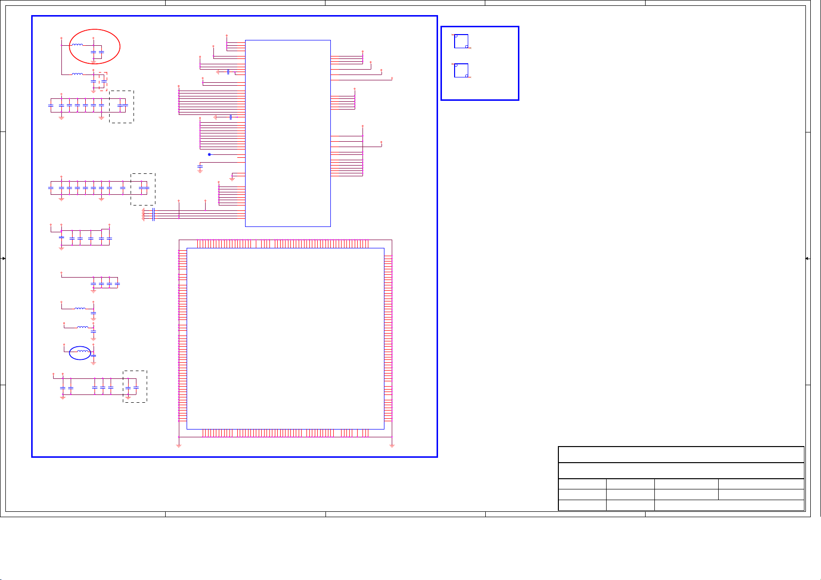
此
Bead
一定要靠近
DC-DC
输出端!电容靠近IC端!
AVDDL_MODVDDC
C241
C241
0.1uF
0.1uF
C267
C267
0.1uF
0.1uF
C252
C252
C260
C260
0.1uF
0.1uF
0.1uF
0.1uF
L205 FBL205 FB
L209
L209
DDR3 POWER
Close to MTS IC
C251
C251
0.1uF
0.1uF
DVDD_DDR
C250
C250
0.1uF
0.1uF
C265
C265
C242
C242
0.1uF
0.1uF
0.1uF
0.1uF
C266
C266
C269
C269
0.1uF
0.1uF
0.1uF
0.1uF
C264
C264
0.1uF
0.1uF
C245
C245
2.2uF
2.2uF
AVDD3P3_MPLL
C262
C262
0.1uF
0.1uF
AVDD_AU33
C261
C261
0.1uF
0.1uF
AVDD3P3_DMPLL
C248
C248
0.1uF
0.1uF
C255
C255
0.1uF
0.1uF
DMPLL
电源隔离!
FOR VB1
C288
C288
1uF
1uF
C295
C295
NC/0.1uF
NC/0.1uF
C243
C243
2.2uF
2.2uF
C273
C273
0.1uF
0.1uF
VDDP_3318
C258
C258
0.1uF
0.1uF
C244
C244
0.1uF
0.1uF
供电,请用
C257
C257
0.1uF
0.1uF
放到IC背部,预留
放到
C290
C290
C291
C291
10uF/X7R
10uF/X7R
0.1uF
0.1uF
C275
C275
C272
C272
0.1uF
0.1uF
0.1uF
0.1uF
C263
C263
0.1uF
0.1uF
C247
C247
C246
C246
0.1uF
0.1uF
0.1uF
0.1uF
Bead FB (10000hm/200mA)
改善ATV
水波纹干扰!
放到IC背部,减小纹波,一定要上件!
C254
C254
C293
C293
0.1uF
0.1uF
10uF/X7R
10uF/X7R
IC
背部,减小纹波,一定要上件!
放到IC背部,减小纹波,一定要上件!
C292
C292
C289
C289
0.1uF
0.1uF
10uF/X7R
10uF/X7R
C277 0.1uFC277 0.1uF
C276 0.1uFC276 0.1uF
C278 0.1uFC278 0.1uF
C279 0.1uFC279 0.1uF
规格和
C294
C294
0.1uF
0.1uF
VDDC
L207 0RL207 0R
D D
C C
B B
C286
C286
10uF/X7R
10uF/X7R
C287
C287
10uF/X7R
10uF/X7R
+1.5V_DDR
10uF/X7R
10uF/X7R
10uF/X7R
10uF/X7R
+3.3V_Normal
VDDC
C239
C239
VDDC_CPU
C249
C249
+3.3V_Standby
+3.3V_Standby
L208 0RL208 0R
C240
C240
0.1uF
0.1uF
Close to MTS IC
C274
C274
0.1uF
0.1uF
AVDD3.3V
C259
C259
2.2uF
2.2uF
Close to MTS IC
Standby Power 3.3V
L206 FBL206 FB
+3.3V_Standby
+3.3V_Standby
FB(1000ohm,200mA)
FB(1000ohm,200mA)
AVDD_DDR
C256
C256
C253
C253
2.2uF
2.2uF
2.2uF
2.2uF
一定要放
D23
AE17
AE2
AB10
AC6
A11
A14
A18
A22
A23
B11
AB24
B14
B18
AA10
B21
B22
B23
C10
C11
C12
C13
C14
C15
C18
C19
C20
C21
C23
D24
D10
D11
D14
D15
D18
D19
D20
D21
AC3
E10
E11
E14
E15
AC4
E18
E19
E20
E24
AE20
C22
AD6
F10
F11
F14
F15
F18
F19
AVDDL_MOD
DVDD_DDR
AVDDL_MOD
VDDC_CPU
TP209TP209
Test pin
!
1
C271
C271
1uF
1uF
AVDD_DDR
AVDD_DDRAVDDL_MOD
U201G
U201G
L10
L11
L12
L13
L15
L16
L20
GND
GND
GNDL9GND
GND
GND
GND
GND
GND
GND
GND
GND
GND
GND
GND
GND
GND
GND
GND
GND
GND
GND
GND
GND
GND
GND
GND
GND
GND
GND
GND
GND
GND
GND
GND
GND
GND
GND
GND
GND
GND
GND
GND
P4
GND
GND
GND
GND
P7
GND
GND
GND
GND
GND
GND
GND
GND
GND
GND
GND
GND
D7
GND
GND
GND
GND
GND
GND
GND
GND
Y3
GND
GNDR7GNDR8GNDR9GND
GND
R10
R11
MSD6A628
MSD6A628
R12
A A
AVDDL_MOD
C268 0.1uFC268 0.1uF
C270 0.1uFC270 0.1uF
DVDD_NODIE
L21
L22
L23
GND
GND
GND
GND
GND
GND
R13
R15
R16
L24
GND
GND
GND
GND
P17
L25
GND
GND
R21
GNDD9GNDM7GNDM8GNDM9GND
GND
R22
4
U201F
U201F
R17
AVDDL_PREDRV
R18
AVDDL_PREDRV
P18
AVDDL_MOD
P19
AVDDL_MOD
P20
AVDDL_RX_USB3
P21
AVDDL_TX_USB3
N18
DVDD_DDR
N19
DVDD_RX_1
N17
DVDD_RX_2
H24
DVDD_DDR_DECAP
H25
DVDD_RX2_DECAP
R20
AVDDL_DVI_PC
R19
AVDDL_DVI_PC
L17
VDDC
L18
VDDC
L19
VDDC
J17
VDDC
M17
VDDC
M18
VDDC
M19
VDDC
K17
VDDC
K19
VDDC
K18
VDDC
P1
VDDC/DECAP
W16
VDDC_CPU
W17
VDDC_CPU
U15
VDDC_CPU
U16
VDDC_CPU
U17
VDDC_CPU
V15
VDDC_CPU
V16
VDDC_CPU
V17
VDDC_CPU
W15
VDDC_CPU
N25
VDDC_CPU/DECAP
P25
VDDC_CPU/DECAP
U12
VSENSE_MIPS
V12
VSENSE_VSS / (TEST POINT)
J24
DVDD_NODIE
L6
GND_EFUSE
H11
TESTPIN / (TEST POINT)
N13
AVDD_DDR0_D
M13
AVDD_DDR0_C
M14
AVDD_DDR0_D
N14
AVDD_DDR0_D
R14
AVDD_DDR1_D
M15
AVDD_DDR1_C
N15
AVDD_DDR1_D
P14
AVDD_DDR1_D
A21
AVDD_DDR0_D/DECAP
D25
AVDD_DDR1_D/DECAP
K25
AVDDL_MOD/DECAP
K24
AVDDL_PREDRV/DECAP
MSD6A628
MSD6A628
M10
M11
M12
M16
M20
GND
GND
GND
GNDT7GNDT8GNDT9GND
GND
GND
GND
T10
T11
T12
T13
T14
3
S1
S1
Heat Sink
1
AVDD33_LAN
A13
AVDD3P3_DADC
B12
AVDD_EAR33
B13
AVDD_NODIE
E12
AVDD_AU33
D12
AVDD3P3_DMPLL
D13
AVDD3P3_MPLL
U13
VDDC_CPU
U14
VDDC_CPU
V13
VDDC_CPU
V14
VDDC_CPU
W13
VDDC_CPU
W14
VDDC_CPU
F17
AVDD3P3_USB
F16
AVDD3P3_DVI
AVDD_MOD (3.3V)
AVDD_MOD (3.3V)
N12
N16
N20
GND
GND
GND
GND
GND
U18
U19
A17
A16
B16
C16
VDDP
D16
VDDP
E16
VDDP
D17
AVDD_PLL
C17
AVDD_PLL
E17
AVDD_PLL
B17
AVDD_PLL
N21
N22
N23
N24
H12
GND
GND
GND
GND
GNDP2GNDP3GND
GNDN1GNDU4GNDV4GNDP8GNDP9GND
GND
GND
GND
GND
GNDV7GNDV8GNDV9GND
GND
V10
V11
V18
U20
U21
U22
U24
VDDP_3318 (3.3V/1.8V)
M21
M22
M23
M24
M25
N10
GND
GNDN2GNDN3GNDR4GNDR5GNDR6GNDN7GNDN8GNDN9GND
GND
GND
GND
GNDU7GNDU8GNDU9GND
T21
T22
N11
GND
GND
GND
GND
GND
GND
T4
U10
U11
W18
W20
W23
GND
GND
GND
GND
GND
GND
GND
GND
GND
GND
GND
T15
T16
T17
T18
T19
T20
GND
P10
GND
V19
VDDC_CPU
P11
P12
GND
GND
GND
GND
V20
V21
AVDD_AU33
AVDD3P3_DMPLL
AVDD3P3_MPLL
AVDD3.3V
VDDP_3318
P13
P16
P22
Y10
W11
W12
GND
GND
GND
GNDW4GND
GND
GND
F20
GND
G7
GND
G8
GND
G9
GND
G10
GND
G11
GND
G13
GND
G14
GND
G15
GND
G16
GND
G17
GND
G18
GND
G19
GND
G20
GND
G24
GND
G25
GND
H7
GND
H8
GND
H9
GND
H10
GND
H13
GND
H14
GND
H15
GND
H16
GND
H17
GND
H18
GND
H19
GND
H20
GND
J7
GND
J8
GND
J9
GND
J10
GND
J11
GND
J12
GND
J13
GND
J14
GND
L14
GND
J16
GND
W19
GND
J18
GND
J19
GND
J20
GND
J22
GND
K7
GND
K8
GND
K9
GND
K10
GND
K11
GND
K12
GND
K13
GND
K14
GND
K15
GND
K16
GND
Y23
GND
AB1
GND
K20
GND
K21
GND
K22
GND
D8
GND
L7
GND
L8
GND
GND
GND
GNDW8GNDW9GND
V22
V23
W10
+3.3V_Standby
A12
Heat-sink58X58mm
Heat-sink58X58mm
S2
S2
Heat-sink35X35mm
Heat-sink35X35mm
2
1
2
2
本文档仅限中国深圳市康冠技术有限公司和被呈送方内部使用,未经书面许可请勿扩散到第三方。
This document for ShenZhen KTC Technology CO., Ltd and presented party internal use only,
Do not spread to third party without the written permission.
版权所有@深圳市康冠技术有限公司
Copyright@ ShenZhen KTC Technology Co., LTD
KTC ISO9001.ISO14001体系文件
KTC ISO9001.ISO14001体系文件
KTC ISO9001.ISO14001体系文件
1
文件名称:
文件名称:
文件名称:
文件编号:
文件编号:
文件编号:
设计:
设计:
设计:
发行部门: 生效日期:
发行部门: 生效日期:
5
4
3
发行部门: 生效日期:
2
MSD6A628方案T8大板DTMB数模一体智能电视原理图
MSD6A628方案T8大板DTMB数模一体智能电视原理图
MSD6A628方案T8大板DTMB数模一体智能电视原理图
T4251
张志清
张志清
张志清
研发处
研发处
研发处
版本:3.0
版本:3.0
版本:3.0
审核:
审核:
审核:
页数:
页数:
页数:
批准:
批准:
批准:
Friday, August 15, 2014
Friday, August 15, 2014
Friday, August 15, 2014
1
58
58
58
of
of
of
76
Page 78
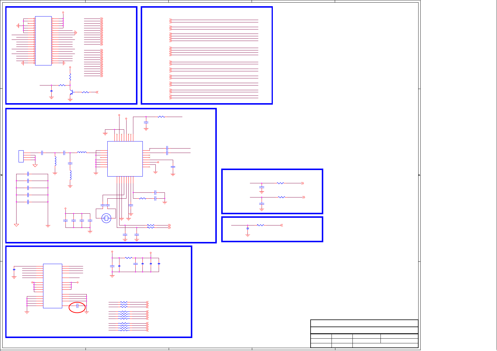
5
VCC
VCC
VCC
P_PWM
GND
E4+
E3+
EC+
E2+
E1+
E0+
O4+
O3+
OC+
O2+
O1+
O0+
GND
接到
12PIN
LVDS_CTL_O
Panel_VCC
2
4
6
8
10
12
14
16
18
20
22
24
26
28
30
32
34
36
38
40
RA3 1KRA3 1K
CC1
CC1
2.2uF/NC
2.2uF/NC
LVDS_CTL_O
B2_RXE3+
B4_RXEC+
B6_RXE2+
G0_RXE1+
G2_RXE0+
G6_RXO4+G7_RXO4G6_RXO3+
R2_RXO2+
R4_RXO1+
R6_RXO0+
RA21KRA2
CN401
CN401
40PIN/2.0mm
40PIN/2.0mm
GND1VCC
GND3VCC
5
NC
7
GND
9
GND
11
GND
13
B3_RXE4- B2_RXE4+
B3_RXE3-
B5_RXEC-
B7_RXE2G1_RXE1G3_RXE0-
D D
G7_RXO3-
R1_RXOC- R0_RXOC+
R3_RXO2R5_RXO1R7_RXO0-
GND
15
E4-
17
E3-
19
EC-
21
E2-
23
E1-
25
E0-
27
O4-
29
O3-
31
OC-
33
O2-
35
O1-
37
O0-
39
GND
LVDS
Net to other page
R7_RXO0R6_RXO0+
R5_RXO1R4_RXO1+
R3_RXO2R2_RXO2+
R1_RXOCR0_RXOC+
G7_RXO3G6_RXO3+
G7_RXO4G6_RXO4+
G3_RXE0G2_RXE0+
G1_RXE1G0_RXE1+
B7_RXE2B6_RXE2+
B5_RXEC-
+3.3V_Normal
1K
B4_RXEC+
B3_RXE3B2_RXE3+
B3_RXE4B2_RXE4+
QA2
QA2
4.7K
4.7K
RA1
RA1
1
3904
3904
2 3
RXO0- 4
RXO0+ 4
RXO1- 4
RXO1+ 4
RXO2- 4
RXO2+ 4
RXOC- 4
RXOC+ 4
RXO3- 4
RXO3+ 4
RXO4- 4
RXO4+ 4
RXE0- 4
RXE0+ 4
RXE1- 4
RXE1+ 4
RXE2- 4
RXE2+ 4
RXEC- 4
RXEC+ 4
RXE3- 4
RXE3+ 4
RXE4- 4
RXE4+ 4
BRI_ADJ 3,4
4
3
2
1
Net
B0M4
B0P4
B1M4
B1P4
B2M4
B2P4
BCKM4
BCKP4
B3M4
B3P4
B4M4
B4P4
A0M4
A0P4
A1M4
A1P4
A2M4
A2P4
ACKM4
ACKP4
A3M4
A3P4
A4M4
A4P4
RXO0RXO0+
RXO1RXO1+
RXE0RXE0+
RXE1RXE1+
RXE2RXE2+
RXECRXEC+
RXE3RXE3+
RXE4RXE4+
VBY0NRXO2VBY0PRXO2+
VBY1NRXOCVBY1PRXOC+
VBY2NRXO3VBY2PRXO3+
VBY3NRXO4VBY3PRXO4+
TDA18275HN
C C
RF SIGNAL INPUT
TUNER_CONNECTOR
TUNER_CONNECTOR
CON1
CON1
RF
1
2
3
4
TC23 10NF/1KVTC23 10NF/1KV
TC24 10NF/1KVTC24 10NF/1KV
TC25 4.7NF/1KVTC25 4.7NF/1KV
TC26 4.7NF/1KVTC26 4.7NF/1KV
TC27 1NF/2KVTC27 1NF/2KV
B B
RF-IN
470nH
TC17 220PFTC17 220PF
TL2
TL2
330nH 140mA 5%
330nH 140mA 5%
+3.3V_TU
TC18
TC18
47NF
47NF
TL3 6.8nHTL3 6.8nHTC29 1NF/2KVTC29 1NF/2KV
TC4
TC4
150pF/NC
150pF/NC
TL1
TL1
220nH 120mA/NC
220nH 120mA/NC
TC19
TC19
47NF
47NF
TC20
TC20
0.1uF
0.1uF
RF_IN#
TC21
TC21
0.1uF
0.1uF
TC9
TC9
33pF
33pF
iNAND FLASH
U1101
NF_CLK
NF_CMD
C1109
C1109
NC/33pF
NC/33pF
NF_D0
NF_D1
NF_D2
NF_D3
A A
U1101
W6
CLK
W5
CMD
H3
D0
H4
D1
H5
D2
J2
D3
RESET
K6
VDD_IF
W4
VDD_IF
Y4
VDD_IF
AA3
VDD_IF
AA5
VDD_IF
K4
iNAND
iNAND
VSS
Y2
VSS
Y5
VSS
AA4
VSS
AA6
CREG/VDDi
VSS
iNAND
iNAND
5
NF_D4
J3
D4
NF_D5
J4
D5
NF_D6
J5
D6
NF_D7
J6
D7
NF_RSTZ
U5
M6
N5
T10
U9
M7
P5
R10
U8
K2
NF_POWERNF_POWER
C1108 2.2uFC1108 2.2uF
VDD
VDD
VDD
VDD
VSS
VSS
VSS
VSS
+3.3V_TU
33
32
GND
GPO1
1
RFG
2
RFIN
3
RFG
4
TESTO1
5
XTSEL
6
TESTO2
7
GNDDIG
8
AS
SCL9SDA10TESTI111XTALP12XTALN13TESTI214VT15CP
XTAL_P
XTAL_N
TC8
TC8
33pF
33pF
TY1 16MHzTY1 16MHz
+3.3V_Normal
C1101
C1101
2.2uF
2.2uF
NF_CLK EMMC_CLK
R1101 10RR1101 10R
NF_CMD
R1102 0RR1102 0R
R1103 0RR1103 0R
RP1101 0RX4
RP1101 0RX4
NF_D4
NF_D6
NF_D7
NF_D5
NF_D1
NF_D3 EMMC_D3
NF_D2
RP1102 0RX4
RP1102 0RX4
+3.3V_TU
30
31
VCCRF
C1102
C1102
0.1uF
0.1uF
7531
7531
7531
7531
28
29
GPO2
VCCIF
GNDIF
R1104 0RR1104 0R
4
25
27
26
AGCD
TESTI3
CAPVCO
16
TC7
TC7
6.8NF
6.8NF
SDA-T
SCL-T
TC12
TC12
33pF
33pF
EMMC_CMD
EMMC_RSTZNF_RSTZ
EMMC_D0NF_D0
EMMC_D4
8642
8642
EMMC_D6
EMMC_D7
EMMC_D5
EMMC_D1
8642
8642
EMMC_D2
AGCA
VCCPL
GNDPL
XTOUT
TC16
TC16
6.8NF
6.8NF
TU3
TU3
TDA18275HN/N1
TDA18275HN/N1
24
IFOAN
23
IFOAP
22
IFODN
21
IFODP
20
19
18
17
TR5 220RTR5 220R
TR1 100RTR1 100R
TR2 100RTR2 100R
TC13
TC13
33pF
33pF
NF_POWER
C1106
C1106
C1105
C1105
0.1uF
0.1uF
2.2uF
2.2uF
TR6 1KTR6 1K
+3.3V_TU
TC10 6.8NFTC10 6.8NF
TC11 150NFTC11 150NF
C1110
C1110
C1107
C1107
0.1uF
0.1uF
0.1uF
0.1uF
EMMC_CLK 4
EMMC_CMD 4
EMMC_RSTZ 4
NAND_RBZ 4
NAND_REZ 4
NAND_CEZ 4
NAND_CE1Z 4
NAND_CLE 4
NAND_ALE 4
NAND_WEZ 4
NAND_WPZ 4
TC14 0.1uFTC14 0.1uF
TC15 0.1uFTC15 0.1uF
IF-AGC
TC6
TC6
0.1uF
0.1uF
T_SDA 4
T_SCL 4
IF-INIF-IN+
DIF IN&OUT
IF-AGC
IF-IN- VIFM
IF-IN+
R1015 100RR1015 100R
C1021
C1021
0.1uF
0.1uF
C821
C821
47pF
47pF
C822
C822
47pF
47pF
Close Tuner
R841 220nHR841 220nH
R840 220nHR840 220nH
VIFP
IF_AGC_T 4
DIF2 4
DIF1 4
AGC RC Filter
本文档仅限中国深圳市康冠技术有限公司和被呈送方内部使用,未经书面许可请勿扩散到第三方。
This document for ShenZhen KTC Technology CO., Ltd and presented party internal use only,
Do not spread to third party without the written permission.
3
2
版权所有
@
深圳市康冠技术有限公司
Copyright@ ShenZhen KTC Technology Co., LTD
KTC ISO9001.ISO14001体系文件
KTC ISO9001.ISO14001体系文件
KTC ISO9001.ISO14001体系文件
文件名称:
文件名称:
文件名称:
MSD6A628方案T8大板DTMB数模一体智能电视原理图
MSD6A628方案T8大板DTMB数模一体智能电视原理图
MSD6A628方案T8大板DTMB数模一体智能电视原理图
文件编号:
文件编号:
文件编号:
设计:
设计:
设计:
发行部门: 生效日期:
发行部门: 生效日期:
发行部门: 生效日期:
T4251
张志清
张志清
张志清
研发处
研发处
研发处
版本:3.0
版本:3.0
版本:3.0
审核:
审核:
审核:
Friday, August 15, 2014
Friday, August 15, 2014
Friday, August 15, 2014
1
页数:
页数:
页数:
批准:
批准:
批准:
of
of
of
68
68
68
77
Page 79
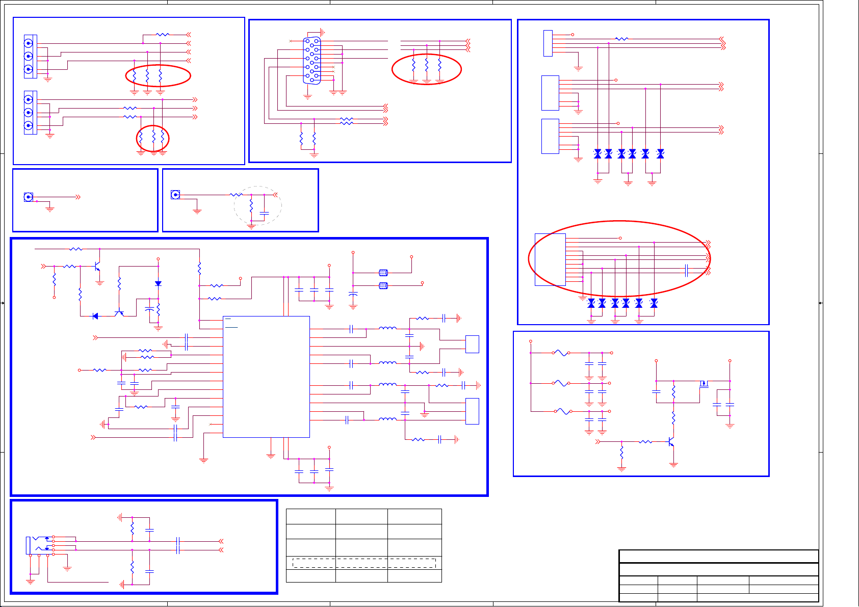
5
4
3
2
1
USB INTERFACE
USB ESD
分布电容要求
5V_USB1
5V_USB2
D630NCD630
1 2
NC
D631NCD631
1 2
NC
D628NCD628
1 2
NC
<2pF
D629NCD629
1 2
NC
USB0_DUSB0_D+
USB1_DUSB1_D+
USB2_DUSB2_D+
WIFI_EN 4
USB0_D- 4
USB0_D+ 4
USB1_D- 4
USB1_D+ 4
USB2_D- 4
USB2_D+ 4
YPBPR&AV2
CN311
CN311
YPBPR_IN
YPBPR_IN
D D
AV1
AV1-AuLin
R534 10KR534 10K
AV1-AuRin
AV1_IN
AV1_IN
CN307
CN307
AV1-IN
R535 10KR535 10K
AV1、AV2、YPbPr
R506
R506
75R
75R
R511 0RR511 0R
R510
R510
75R
75R
R536
R536
R537
R537
12K
12K
12K
12K
AV2_IN 4
YPbPr_Y 4
YPbPr_PB 4
YPbPr_PR 4
R509
R509
75R
75R
AV1_IN 4
AV1-Lin 4
AV1-Rin 4
R538
R538
75R
75R
Close to Mstar IC
四者共用音频输入接口
VGA
CON601
CON601
11
12
13
14
15
R615
R615
10K
10K
CN207
1617
1
6
2
7
3
8
4
9
5
10
VGA
VGA
R618
R618
10K
10K
DDC_SCL_D
DDC_SDA_D
R622100R R622100R
R617100R R617100R
VGA-Rin
VGA-Gin
VGA-Bin
VGA-Bin
VGA-Gin
VGA-Rin
R616
R616
R620
R620
R621
R621
75R
75R
75R
75R
75R
75R
Close to Mstar IC
UART_RX 4
UART_TX 4
VGA_VSYNC 4
VGA_HSYNC 4
VGA-Bin 4
VGA-Gin 4
VGA-Rin 4
CN207
1
2
3
4
5
CON5-2.0mm
CON5-2.0mm
VCC
D-
D+
GND
SHIELD
SHIELD
CN317
CN317
VCC
D-
D+
GND
SHIELD
SHIELD
CN318
CN318
1
2
3
4
5
6
USB_4P
USB_4P
1
2
3
4
5
6
USB_4P
USB_4P
5V_USB_WIFI
R17 100R/NCR17 100R/NC
D625NCD625
D627NCD627
1 2
1 2
NC
NC
1
2
3
4
5
6
7
8
9
10
11
12
13
14
R415 0RR415 0R
U202
U202
SD
FAULT
LINP
LINN
GAIN0
GAIN1
AVCC
AGND
GVDD
PLIMIT
RINN
RINP
NC
PBTL
TPA3110LD2
TPA3110LD2
Close to Mstar IC
R410
R410
75R
75R
+5V_Normal
C401
C401
100pF
100pF
29
TAB
CVBS1_OUT 4
C169
C169
1nF
1nF
28
BSPL
PVCCL27PVCCL
OUTPL
PGND
OUTNL
BSNL
BSNR
OUTNR
PGND
OUTPR
BSPR
PVCCR15PVCCR
16
C175
C175
1nF
1nF
26
25
24
23
22
21
20
19
18
17
C321
C321
100nF
100nF
C222
C222
100nF
100nF
AMP_12V
C317
C317
10uF/16V
10uF/16V
OUTPL
OUTNL
OUTNR
OUTPR
AMP_12V1
C1
10uF/16VC110uF/16V
+12V_NORMAL
C221
C221
470uF
470uF
C322 0.22UFC322 0.22UF
C297
C297
C299
C299
C300 0.22UFC300 0.22UF
0.22UF
0.22UF
0.22UF
0.22UF
L204
L204
0805_BEAD
0805_BEAD
L210
L210
0805_BEAD
0805_BEAD
22UH/600
22UH/600
22UH/600
22UH/600
22UH/600
22UH/600
22UH/600
22UH/600
CON602
CON602
USB3-A/USB3.0
USB3-A/USB3.0
AMP_12V
AMP_12V1
R4 10R/NCR4 10R/NC
C4 330PF/NCC4 330PF/NC
L5
L5
欧磁珠
4A
欧磁珠
4A
C316
C316
0.47UF
0.47UF
C318
欧磁珠
欧磁珠
欧磁珠
欧磁珠
欧磁珠
欧磁珠
4A
4A
4A
4A
4A
4A
C318
0.47UF
0.47UF
R1 10R/NCR1 10R/NC
C315
C315
0.47UF
0.47UF
C314
C314
0.47UF
0.47UF
R5 10R/NCR5 10R/NC
R2 10R/NCR2 10R/NC
ROUT-
C5 330PF/NCC5 330PF/NC
L10
L10
L14
L14
L23
L23
LOUT+
LOUT-
C2 330PF/NCC2 330PF/NC
ROUT+
CN203CN203
2
1
C3 330PF/NCC3 330PF/NC
CN201
CN201
1
-
2
GND
3
+
3Pin/2.0mm
3Pin/2.0mm
+5V_Normal
STDA_SSRX-
STDA_SSRX+
STDA_SSTX-
STDA_SSTX+
VBUS
GND
GND_DRAIN
SHELL
SHELL
1
2
D-
3
D+
4
5
6
7
8
9
10
11
1 2
L4036V/1.1A L4036V/1.1A
C619
C619
0.1uF
0.1uF
L4046V/1.1A L4046V/1.1A
C618
C618
0.1uF
0.1uF
L4056V/1.1A L4056V/1.1A
C617
C617
0.1uF
0.1uF
USB3_EN4
H :Power on
L :Power off
D626NCD626
NC
D636NCD636
1 2
NC
C603
C603
10uF
10uF
C604
C604
10uF
10uF
C605
C605
10uF
10uF
5V_USB3
D634NCD634
1 2
NC
5V_USB_WIFI
5V_USB1
5V_USB2
D635NCD635
1 2
NC
R47 4.7KR47 4.7K
R44
R44
10K
10K
D632NCD632
1 2
NC
+5V_Normal
D633NCD633
1 2
NC
USB3.0
USB3_D- 4
USB3_D+ 4
USB3_SSRXN 4
Q14 AO3401Q14 AO3401
电容靠近
USB3_SSRXP 4
USB3_SSTXN 4
USB3_SSTXP 4
5V_USB3
C51
C51
C61
C61
0.1uF
0.1uF
10uF
10uF
USB)端子,提供usb
读写稳定性
C616 0.1uFC616 0.1uF
C615 0.1uFC615 0.1uF
R59
R59
C68
C68
100K
100K
1uF
1uF
USB3_ON
R45
R45
10K
10K
Note:
Q13
Q13
1
2 3
3904
3904
USB POWER
VIDEO-OUT/YELLOW
AMP_12V
D205
D205
1N4148
1N4148
R236
R236
100k
100k
C226 0.47uFC226 0.47uF
AV-OUT
C225 0.47uFC225 0.47uF
VIDEO-OUT/YELLOW
CN315
CN315
AVOUT-V
1
2
R2611KR261
1K
R268 100k/ncR268 100k/nc
R267 100kR267 100k
L:SHUTDOWN
SD
C319 0.47uFC319 0.47uF
LIN_P
LIN_N
C320 0.47uFC320 0.47uF
GAIN0
GAIN1
AVCC
GVDD
PLMIT
C298
C298
RIN_N
1uF
1uF
RIN_P
Coaxial
Coaxial
CN314
CN314
1
2
Coaxial OUT
C C
AMP-MUTE4
L:ON
H:MUTE
+3.3V_Standby
B B
R274 0RR274 0R
R273 10kR273 10k
R275
R275
4.7k
4.7k
EARPHONE-OUTL4
AMP_12V
EARPHONE-OUTR4
SPDIFOUT 4
1
R248
R248
10K
10K
D204 1N4148D204 1N4148
R255 10RR255 10R
SHUTDOWNHP_MUTE
Q26
Q26
3904
3904
2 3
R238
R238
10K
10K
1
C296
C296
Q206
Q206
100uF/16V
100uF/16V
23
3906
3906
R258 10k/NCR258 10k/NC
R249 10kR249 10k
R250 10kR250 10k
C142
C142
C165
C165
100nF
100nF
10uF/16V
10uF/16V
R240 10kR240 10k
C323
C323
1uF
1uF
AUDIO AMP
功放放大倍数调节
EARPHONE OUT
HP/BLUE
HP/BLUE
A A
CN22
CN22
678
5
4
2
1
3
E_AMP-L
E_AMP-R
HP_MUTE
5
R271
R271
47k
47k
R272
R272
47k
47k
C327
C327
1nF
1nF
C328
C328
1nF
1nF
C326 10ufC326 10uf
C329 10ufC329 10uf
EARPHONE-OUTL 4
EARPHONE-OUTR 4
4
GAIN1(PIN6) GAIN0(PIN5)
0
0
01
1
0
1
AMP GAIN(db)
20
26
32
361
3
本文档仅限中国深圳市康冠技术有限公司和被呈送方内部使用,未经书面许可请勿扩散到第三方。
This document for ShenZhen KTC Technology CO., Ltd and presented party internal use only,
Do not spread to third party without the written permission.
2
版权所有@深圳市康冠技术有限公司
Copyright@ ShenZhen KTC Technology Co., LTD
KTC ISO9001.ISO14001体系文件
KTC ISO9001.ISO14001体系文件
KTC ISO9001.ISO14001体系文件
MSD6A628方案T8大板DTMB数模一体智能电视原理图
文件名称:
MSD6A628方案T8大板DTMB数模一体智能电视原理图
文件名称:
MSD6A628方案T8大板DTMB数模一体智能电视原理图
文件名称:
文件编号:
文件编号:
文件编号:
设计:
设计:
设计:
发行部门: 生效日期:
发行部门: 生效日期:
发行部门: 生效日期:
T4251
张志清
张志清
张志清
研发处
研发处
研发处
版本:3.0
版本:3.0
版本:3.0
审核:
审核:
审核:
Friday, August 15, 2014
Friday, August 15, 2014
Friday, August 15, 2014
1
页数:
页数:
页数:
批准:
批准:
批准:
of
of
of
78
78
78
78
Page 80
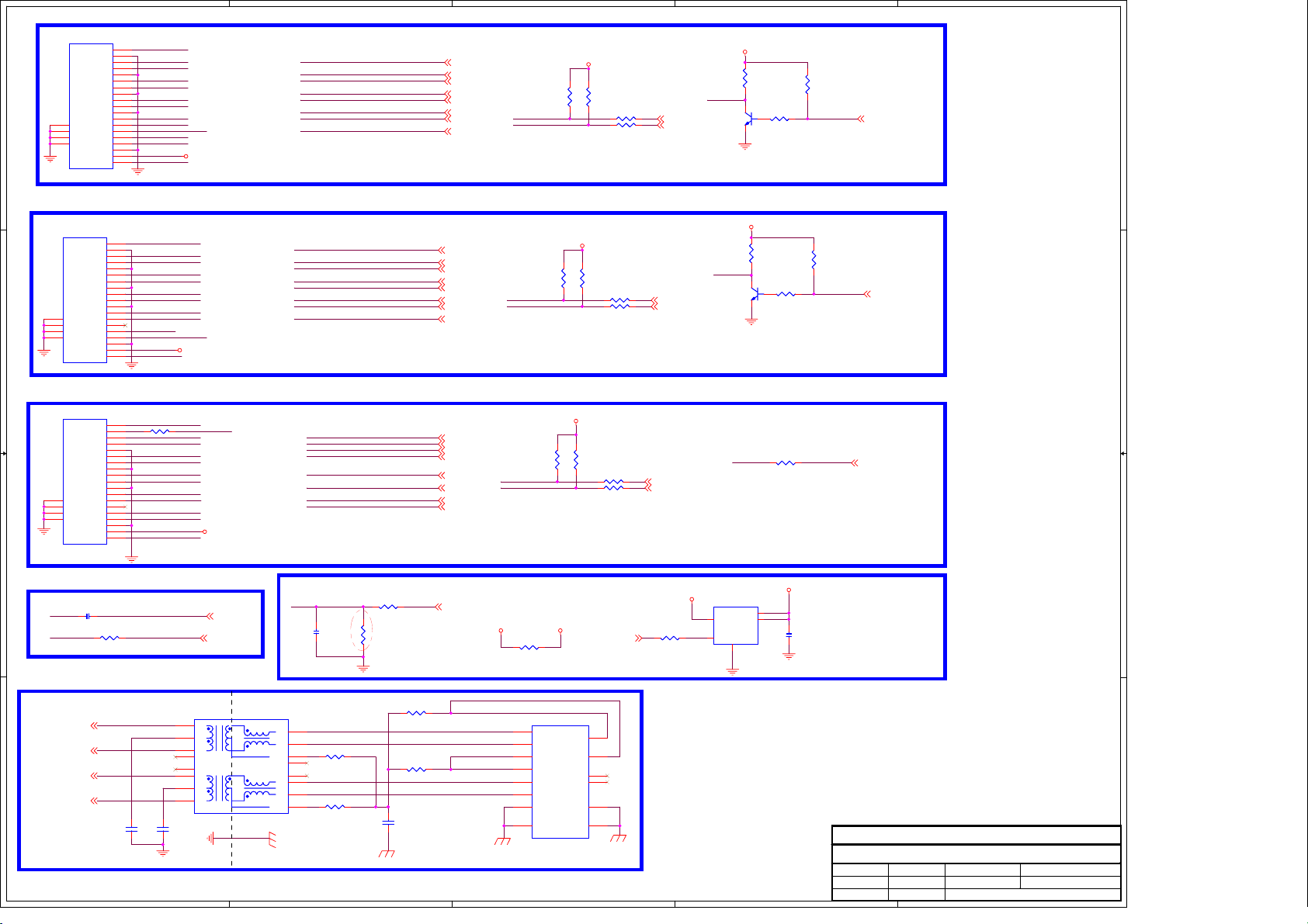
5
4
3
2
1
HDMI1(ARC)
CON801
CON801
DATA2+
DATA2 SHIELD
DATA2-
DATA1+
DATA1 SHIELD
DAT1A-
DATA0+
DATA0 SHIELD
DATA0-
CLK+
CLK SHIELD
D D
20
GND1
21
GND2
22
GND3
23
GND3
DDC/CEC GND
CLKCEC
+5V POWER
HOT PLUG
HDMI/90D
HDMI/90D
SCL
SDA
HDMI1_RX2P
1
2
HDMI1_RX2N
3
HDMI1_RX1P
4
5
HDMI1_RX1N
6
HDMI1_RX0P
7
8
HDMI1_RX0N
9
HDMI1_CLKP
10
11
HDMI1_CLKN
12
CEC
13
HDMI1_ARC
14
NC
HDMI1-DDC-SCL
15
HDMI1-DDC-SDA
16
17
18
19
HDMI1-HPD
HDMI1/5V
HDMI1-RX2PHDMI1_RX2P
HDMI1-RX2NHDMI1_RX2N
HDMI1-RX1PHDMI1_RX1P
HDMI1-RX1NHDMI1_RX1N
HDMI1-RX0PHDMI1_RX0P
HDMI1-RX0NHDMI1_RX0N
HDMI1-CLKPHDMI1_CLKP
HDMI1-CLKNHDMI1_CLKN
HDMI1-RX2P 4
HDMI1-RX2N 4
HDMI1-RX1P 4
HDMI1-RX1N 4
HDMI1-RX0P 4
HDMI1-RX0N 4
HDMI1-CLKP 4
HDMI1-CLKN 4
HDMI1-DDC-SCL
HDMI1-DDC-SDA
HDMI1/5V
R803
R803
10K
10K
R804
R804
10K
10K
R801 33RR801 33R
R806 33RR806 33R
HDMI1-SDA 4
HDMI1-HPD
HDMI1/5V
R8021KR802
1K
3904
3904
2 3
Q801
Q801
R807 10KR807 10K
1
R805
R805
10K
10K
HDMI1-HPDIN
HDMI1-HPDIN 4HDMI1-SCL 4
HDMI2
HDMI2-HPD
HDMI2/5V
R8081KR808
1K
3904
3904
2 3
Q802
Q802
1
R814 10KR814 10K
R809
R809
10K
10K
HDMI2-HPDIN
HDMI2-HPDIN 4
CON802
CON802
DATA2+
DATA2 SHIELD
DATA2-
DATA1+
DATA1 SHIELD
DAT1A-
DATA0+
DATA0 SHIELD
DATA0-
CLK+
CLK SHIELD
CLK-
20
CEC
GND1
21
GND2
22
SCL
GND3
23
SDA
C C
GND3
DDC/CEC GND
+5V POWER
HOT PLUG
HDMI/90D
HDMI/90D
HDMI2_RX2P
1
2
HDMI2_RX2N
3
HDMI2_RX1P
4
5
HDMI2_RX1N
6
HDMI2_RX0P
7
8
HDMI2_RX0N
9
HDMI2_CLKP
10
11
HDMI2_CLKN
12
CEC
13
14
NC
HDMI2-DDC-SCL
15
HDMI2-DDC-SDA
16
17
18
19
HDMI2-HPD
HDMI2/5V
HDMI2-RX2PHDMI2_RX2P
HDMI2-RX2NHDMI2_RX2N
HDMI2-RX1PHDMI2_RX1P
HDMI2-RX1NHDMI2_RX1N
HDMI2-RX0PHDMI2_RX0P
HDMI2-RX0NHDMI2_RX0N
HDMI2-CLKPHDMI2_CLKP
HDMI2-CLKNHDMI2_CLKN
HDMI2-RX2P 4
HDMI2-RX2N 4
HDMI2-RX1P 4
HDMI2-RX1N 4
HDMI2-RX0P 4
HDMI2-RX0N 4
HDMI2-CLKP 4
HDMI2-CLKN 4
HDMI2-DDC-SCL
HDMI2-DDC-SDA
R810
R810
10K
10K
HDMI2/5V
R811
R811
10K
10K
R812 33RR812 33R
R813 33RR813 33R
HDMI2-SCL 4
HDMI2-SDA 4
HDMI3(MHL)
CON803
CON803
DATA2+
DATA2 SHIELD
DATA2-
DATA1+
DATA1 SHIELD
DAT1A-
DATA0+
DATA0 SHIELD
DATA0-
CLK+
CLK SHIELD
CLK-
20
CEC
GND1
21
GND2
22
SCL
GND3
23
SDA
GND3
DDC/CEC GND
+5V POWER
HOT PLUG
HDMI/90D
HDMI/90D
B B
CEC & ARC
HDMI1_ARC HDMI-ARC
C801
C801
2.2uF
2.2uF
CEC
R822 200RR822 200R
HDMI3_RX2P
1
R850 0RR850 0R
HDMI3_RX2N
HDMI3_RX1P
HDMI3_RX1N
HDMI3_RX0P
HDMI3_RX0N
HDMI3_CLKP
HDMI3_CLKN
CEC
HDMI3-DDC-SCL
HDMI3-DDC-SDA
HDMI3-HPD
MHL_CD_SENSE
HDMI3/5V
HDMI1-ARC 4
MHL_CD_SENSE
C802
C802
47nF
47nF
R848
R848
300K
300K
HDMI3-RX2PHDMI3_RX2P
HDMI3-RX2NHDMI3_RX2N
HDMI3-RX1PHDMI3_RX1P
HDMI3-RX1NHDMI3_RX1N
HDMI3-RX0PHDMI3_RX0P
HDMI3-RX0NHDMI3_RX0N
HDMI3-CLKPHDMI3_CLKP
HDMI3-CLKNHDMI3_CLKN
R849 100RR849 100R
HDMI3-RX2P 4
HDMI3-RX2N 4
HDMI3-RX1P 4
HDMI3-RX1N 4
HDMI3-RX0P 4
HDMI3-RX0N 4
HDMI3-CLKP 4
HDMI3-CLKN 4
MHL_Cable_DET 4
HDMI3-DDC-SCL
HDMI3-DDC-SDA
HDMI3/5V
R851 10RR851 10R
2
3
4
5
6
7
8
9
10
11
12
13
14
NC
15
16
17
18
19
+5V_Standby
R816
R816
R817
R817
10K
10K
10K
10K
AVDD5V_MHL
R819 33RR819 33R
R820 33RR820 33R
MHL_Cable_DET4HDMI-CEC 4
HDMI3-SCL 4
HDMI3-SDA 4
+5V_Normal
R854 0RR854 0R
HDMI3-HPD HDMI3-HPDIN
QA801
QA801
VOUT
3
VOUT
IN
4
EN
GND
2
SGM2554A
SGM2554A
R852 33RR852 33R
5
1
HDMI3/5V
C803
C803
0.1uF
0.1uF
HDMI3-HPDIN 4
MHL
HST-0041
HST-0041
U651
C654
C654
0.1uF
0.1uF
U651
1
TD+
2
TCT
3
TD-
4
NC1
5
NC2
6
RD+
7
RCT
8
RD-
SMDTR16P
SMDTR16P
TCM-
16
TX+
14
TX-
R660 75R/1%R660 75R/1%
15
TCM
13
NC4
12
NC3
11
RX+
9
RX-
R664 75R/1%R664 75R/1%
10
MDI_TP
MDI_TP4
MDI_TN
MDI_TN4
MDI_RP
A A
MDI_RP4
MDI_RN
MDI_RN4
C653
C653
0.1uF
0.1uF
LAN
5
4
R657 75R/1%R657 75R/1%
R662 75R/1%R662 75R/1%
CB652
CB652
1nF/2KV
1nF/2KV
CN309
CN309
1
TD+
2
TD-
4
TDCT
5
RDCT
3
RD+
6
RDGND112GND2
10
GND3
RJ45-W
RJ45-W
CH_GND
GND4
3
7
NC
8
13
NC1
14
NC2
11
9
本文档仅限中国深圳市康冠技术有限公司和被呈送方内部使用,未经书面许可请勿扩散到第三方。
This document for ShenZhen KTC Technology CO., Ltd and presented party internal use only,
Do not spread to third party without the written permission.
2
版权所有
@
深圳市康冠技术有限公司
Copyright@ ShenZhen KTC Technology Co., LTD
KTC ISO9001.ISO14001体系文件
KTC ISO9001.ISO14001体系文件
KTC ISO9001.ISO14001体系文件
MSD6A628方案T8大板DTMB数模一体智能电视原理图
MSD6A628方案T8大板DTMB数模一体智能电视原理图
MSD6A628方案T8大板DTMB数模一体智能电视原理图
文件名称:
文件名称:
文件名称:
文件编号:
文件编号:
文件编号:
设计:
设计:
设计:
发行部门: 生效日期:
发行部门: 生效日期:
发行部门: 生效日期:
T4251
张志清
张志清
张志清
研发处
研发处
研发处
版本:3.0
版本:3.0
版本:3.0
审核:
审核:
审核:
Friday, August 15, 2014
Friday, August 15, 2014
Friday, August 15, 2014
1
页数:
页数:
页数:
批准:
批准:
批准:
of
of
of
88
88
88
79
 Loading...