

Philips 32PFL9432/98, 42PFL9532/9x_1, 47PFL9532/9x_1, 47PFL9532/9x_2, 42PFL9532/9x_2 Service Manual
...
Colour Television Chassis
AUREA
ME7
Q528.1A
LA
AUREA
ME7
Contents Page Contents Page
1. Technical Specifications, Connections, and Chassis
Overview 2
2. Safety Instructions, Warnings, and Notes 6
3. Directions for Use 7
4. Mechanical Instructions 8
5. Service Modes, Error Codes, and Fault Finding 25
6. Block Diagrams, Test Point Overview, and
Waveforms
Wiring Diagram 32” LCD 49
Wiring Diagram 42” LCD 50
Wiring Diagram 47” 51
Wiring Diagram 42” (AUREA) 52
Block Diagram Supply 32” 53
Block Diagram Supply 37” - 42” 54
Block Diagram Supply 47” 55
Block Diagram Supply Audio & AmbiLight 56
Block Diagram Video 57
Block Diagram Audio 58
Block Diagram Control & Clock Signals 59
Testpoint Overview Small Signal Board 60-65
I2C IC Overview 66
Supply Lines Overview 67
7. Circuit Diagrams and PWB Layouts Drawing PWB
Display Supply (32”): Part 1 (A1) 68 70-71
Display Supply (32”): Part 2 (A2) 69 70-71
Display Supply (42”): Mains Filter & Standby(A1)72 75-76
Display Supply (42”): Supply (A2) 73 75-76
Display Supply (42”): DC - DC (A3) 74 75-76
DFI Panel: DC - DC (AB1) 77 87-88
DFI Panel: Video Flow (AB2) 78 87-88
DFI Panel: Clock (AB3) 79 87-88
DFI Panel: Supply (AB4) 80 87-88
DFI Panel: FPGA: Power & Control (AB5) 81 87-88
DFI Panel: FPGA: DFI (AB6) 82 87-88
©
Copyright 2007 Philips Consumer Electronics B.V. Eindhoven, The Netherlands.
All rights reserved. No part of this publication may be reproduced, stored in a
retrieval system or transmitted, in any form or by any means, electronic,
mechanical, photocopying, or otherwise without the prior permission of Philips.
DFI Panel: DDR A (AB7) 83 87-88
DFI Panel: DDR B (AB8) 84 87-88
DFI Panel: Display Interfacing (AB9) 85 87-88
DFI Panel: FPGA Ambilight (AB10) 86 87-88
AmbiLight Panel (5 LED) (AL1) 89 91
AmbiLight Panel (5 LED) (AL2) 90 91
AmbiLight Panel (3 Side 4 LED) (AL1) 92 94
AmbiLight Panel (3 Side 4 LED) (AL2) 93 94
Audio & AL Supply Panel: Supply (AP1) 95 100-101
Audio & AL Supply Panel: Audio (AP2A) 96 100-101
Audio & AL Supply Panel: Protection (AP2B) 97 100-101
Audio & AL Supply Panel: Subwoofer (AP2C) 98 100-101
Audio & AL Supply Panel: Centre Input (AP2D) 99 100-101
Small Signal Board (B1-B11) 102-143 147-152
SSB: SRP List 144-146
Side I/O Panel (D) 153 154
Keyboard Control Panel (E) 155 156
Front IR / LED Panel (J) 158 159
8. Alignments 161
9. Circuit Descriptions, Abbreviation List, and IC Data
Sheets 164
Abbreviation List 185
IC Data Sheets 188
10. Spare Parts and Diversity List 197
11. Revision List 215
H_16790_000.eps
101007
Published by EL 0770 BU CD Customer Service Printed in the Netherlands Subject to modification EN 3122 785 16791

EN 2 Q528.1A LA1.
Technical Specifications, Connections, and Chassis Overview
1. Technical Specifications, Connections, and Chassis Overview
Index of this chapter:
1.1 Technical Specifications
1.2 Connections
1.3 Chassis Overview
Notes:
• Figures can deviate due to the different set executions.
• Specifications are indicative (subject to change).
1.1 Technical Specifications
1.1.1 Vision
Display type : LCD
Screen size : 32" (82 cm), 16:9
: 42" (107 cm), 16:9
: 47" (120 cm), 16:9
Resolution (H × V pixels) : 1366 × 768p (32")
: 1920 × 1080p (42")
Light output (cd/m
Viewing angle (H × V degrees) : 176 × 176
Tuning system : PLL
Colour systems : PAL B/G
Video playback : NTSC
Tuner bands : UHF, VHF, S, Hyper
Supported video formats : 480i @ 60 Hz
Supported computer formats (60 Hz) : 640 × 480
2
) : 550
: 1920 × 1080p (47")
: PAL I
: SECAM B/G
: SECAM D/K
: PAL
: SECAM
: 480p @ 60 Hz
: 576i @ 50 Hz
: 576p @ 50 Hz
: 720p @ 50/60 Hz
: 1080i @ 50/60 Hz
: 1080p @ 24/25/30/
50/60 Hz
: 800 × 600
: 1024 × 768
: 1280 × 1024
: 1360 × 768
: 1920 × 1080i
: 1920 × 1080p
1.1.3 Multimedia
Supported file formats : JPEG
USB input : USB2.0
1.1.4 Miscellaneous
Power supply:
- Mains voltage (V
- Mains frequency (Hz) : 50 / 60
Ambient conditions:
- Temperature range (°C) : +5 to +35
Power consumption (values are indicative)
- Normal operation (W) : 132 (32")
- Standby (W) : 0.8
Dimensions (W × H × D in mm) : 805 × 547 × 115 (32")
Weight (kg) : 14.3 (32")
) : 220 - 240 ±10%
AC
:MP3
: Slideshow (.alb)
: 232 (42")
: 275 (47")
: 1046 × 686 × 116
(42")
: 1121 × 715 × 129
(42PFL9900)
: 1157 × 752 × 117
(47")
: 26.1 (42")
: 36.8 (42PFL9900)
: 32.0 (47")
1.1.2 Sound
Maximum power (W
):2 × 8
RMS
:2 × 12 (42PFL9900)

Technical Specifications, Connections, and Chassis Overview
1.2 Connections
EN 3Q528.1A LA 1.
Rear connectors
MONITOR
OUT
R
VIDEO
L
DISPLAY SYNCHRONIZED
AUDIO
DIGITAL AUDIO
DISPLAY
SYNC.
Note: The following connector colour abbreviations are used
(acc. to DIN/IEC 757): Bk= Black, Bu= Blue, Gn= Green,
Gy= Grey, Rd= Red, Wh= White, Ye= Yellow.
1.2.1 Side Connections
USB2.0
1234
Figure 1-2 USB (type A)
1-+5V k
2 -Data (-) jk
3 -Data (+) jk
4 -Ground Gnd H
Headphone (Output)
Bk - Headphone 32 - 600 ohm / 10 mW ot
Cinch: Video CVBS - In, Audio - In
Rd - Audio R 0.5 V
Wh - Audio L 0.5 V
Ye - Video CVBS 1 V
ANALOG AUDIO IN
VGA / HDMI 1 / HDMI 2
IN
OUT
R
L
E_06532_022.eps
300904
/ 10 kohm jq
RMS
/ 10 kohm jq
RMS
/ 75 ohm jq
PP
SERVICE
UART
Figure 1-1 Connection overview
HDMI 1, 2 & 3: Digital Video, Digital Audio - In
1 - D2+ Data channel j
2 - Shield Gnd H
3 - D2- Data channel j
4 - D1+ Data channel j
5 - Shield Gnd H
6 - D1- Data channel j
7 - D0+ Data channel j
8 - Shield Gnd H
9 - D0- Data channel j
10 - CLK+ Data channel j
11 - Shield Gnd H
12 - CLK- Data channel j
13 - n.c.
14 - n.c.
15 - DDC_SCL DDC clock j
16 - DDC_SDA DDC data jk
17 - Ground Gnd H
18 - +5V j
19 - HPD Hot Plug Detect j
20 - Ground Gnd H
AV 3
L
AUDIO
R
S VIDEO
AV 1
YPbPr
VIDEO L RAUDIO
AV 2
VIDEO
Y
Pb Pr
19
18 2
E_06532_017.eps
AUDIOLR
1
250505
Figure 1-3 HDMI (type A) connector
Side
H_16790_054.eps
220807
S-Video (Hosiden): Video Y/C - In
1 -Ground Y Gnd H
2 -Ground C Gnd H
3 - Video Y 1 V
4 - Video C 0.3 V
/ 75 ohm j
PP
/ 75 ohm j
PP
1.2.2 Rear Connections
Monitor Out: Cinch: Video CVBS - Out, Audio - Out
Ye - Video CVBS 1 V
Rd - Audio R 0.5 V
Wh - Audio L 0.5 V
/ 75 ohm kq
PP
/ 10 kohm kq
RMS
/ 10 kohm kq
RMS
Digital Audio In: Cinch: S/PDIF - In
Bk - Coaxial 0.2 - 0.6V
/ 75 ohm jq
PP
Digital Audio Out: Cinch: S/PDIF - Out
Bk - Coaxial 0.4 - 0.6V
/ 75 ohm kq
PP
Cinch: Audio - In
Rd - Audio - R 0.5 V
Wh - Audio - L 0.5 V
/ 10 kohm kq
RMS
/ 10 kohm kq
RMS
Service Connector (UART): Jack 3.5 mm
1 - Ground Gnd H
2 - UART_TX Transmit k
3 - UART_RX Receive j
Aerial - In
- - F-type (US) Coax, 75 ohm D
AV3: Cinch: Audio - In
Rd - Audio - R 0.5 V
Wh - Audio - L 0.5 V
/ 10 kohm kq
RMS
/ 10 kohm kq
RMS
AV3: Cinch: Video YPbPr - In
Gn -Video Y 1 V
Bu - Video Pb 0.7 V
Rd - Video Pr 0.7 V
/ 75 ohm jq
PP
/ 75 ohm jq
PP
/ 75 ohm jq
PP
AV2: Cinch: Video CVBS - In, Audio - In
Rd - Audio R 0.5 V
Wh - Audio L 0.5 V
Ye - Video CVBS 1 V
/ 10 kohm jq
RMS
/ 10 kohm jq
RMS
/ 75 ohm jq
PP
EN 4 Q528.1A LA1.
Technical Specifications, Connections, and Chassis Overview
AV1: S-Video (Hosiden): Video Y/C - In
1 - Ground Y Gnd H
2 - Ground C Gnd H
3 - Video Y 1 V
4 - Video C 0.3 V
AV1: Cinch: Video CVBS - In, Audio - In
Rd - Audio R 0.5 V
/ 75 ohm j
PP
/ 75 ohm j
PP
/ 10 kohm jq
RMS
1.3 Chassis Overview
DISPLAY
A
SUPPLY PANEL
Wh - Audio L 0.5 V
Ye - Video CVBS 1 V
AV1: Cinch: Video YPbPr - In
Gn - Video Y 1 V
Bu - Video Pb 0.7 V
Rd - Video Pr 0.7 V
PP
PP
/ 10 kohm jq
RMS
/ 75 ohm jq
/ 75 ohm jq
/ 75 ohm jq
PP
/ 75 ohm jq
PP
SIDE I/O PANEL
KEYBOARD CONTROL
PA NE L
D
E
SMALL SIGNAL
B
BOARD
DISPLAY
A
SUPPLY PANEL
SMALL SIGNAL
B
BOARD
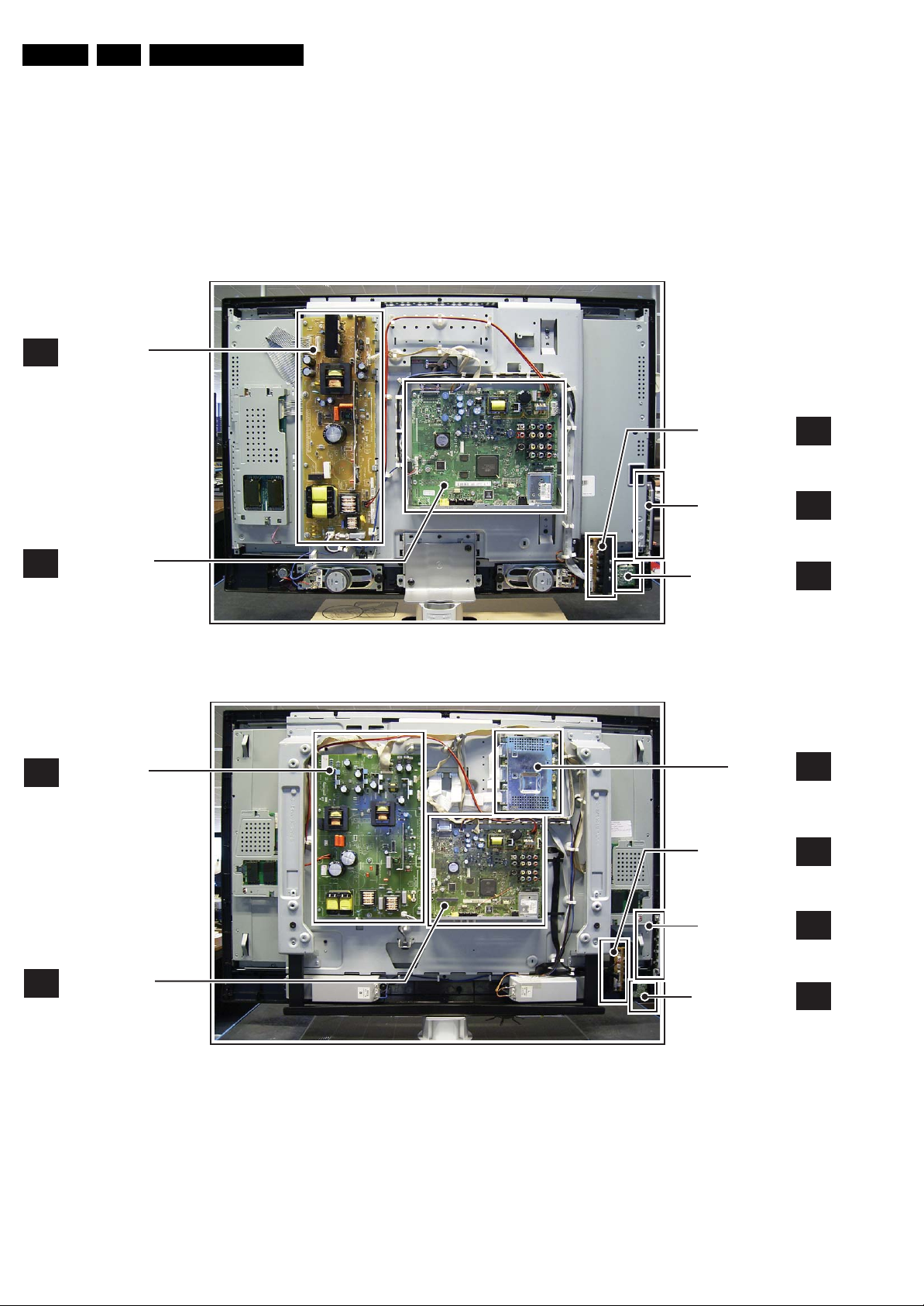
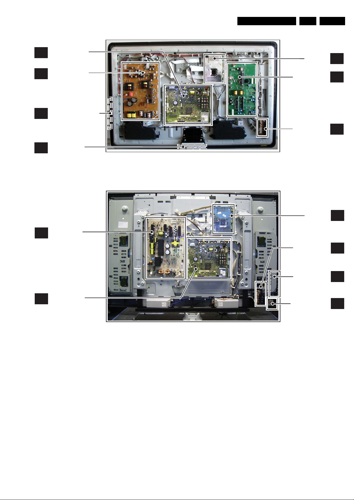
Figure 1-4 PWB/CBA locations 32" sets
IR & LED PANEL
H_16790_055.eps
DFI PANEL
SIDE I/O PANEL
KEYBOARD CONTROL
PANEL
IR & LED PANEL
J
230807
AB
D
E
J
Figure 1-5 PWB/CBA locations 42" ME7 styling sets
H_16790_056.eps
230807
SMALL SIGNAL
B
BOARD
Technical Specifications, Connections, and Chassis Overview
DFI PANEL
EN 5Q528.1A LA 1.
AB
DISPLAY SUPPLY
A
PANEL
KEYBOARD CONTROL
E
PANEL
IR & LED PANEL
J
DISPLAY
A
SUPPLY PANEL
Figure 1-6 PWB/CBA locations 42" Aurea styling sets
STANDBY/AUDIO
PANEL
SIDE I/O PANEL
H_16790_075.eps
DFI PANEL
AP
D
111007
AB
SMALL SIGNAL
B
BOARD
Figure 1-7 PWB/CBA locations 47" sets
SIDE I/O PANEL
KEYBOARD CONTROL
PANEL
IR & LED PANEL
H_16790_057.eps
D
E
J
230807

EN 6 Q528.1A LA2.
Safety Instructions, Warnings, and Notes
2. Safety Instructions, Warnings, and Notes
Index of this chapter:
2.1 Safety Instructions
2.2 Warnings
2.3 Notes
2.1 Safety Instructions
Safety regulations require the following during a repair:
• Connect the set to the Mains/AC Power via an isolation
transformer (> 800 VA).
• Replace safety components, indicated by the symbol h,
only by components identical to the original ones. Any
other component substitution (other than original type) may
increase risk of fire or electrical shock hazard.
Safety regulations require that after a repair, the set must be
returned in its original condition. Pay in particular attention to
the following points:
• Route the wire trees correctly and fix them with the
mounted cable clamps.
• Check the insulation of the Mains/AC Power lead for
external damage.
• Check the strain relief of the Mains/AC Power cord for
proper function.
• Check the electrical DC resistance between the Mains/AC
Power plug and the secondary side (only for sets that have
a Mains/AC Power isolated power supply):
1. Unplug the Mains/AC Power cord and connect a wire
between the two pins of the Mains/AC Power plug.
2. Set the Mains/AC Power switch to the “on” position
(keep the Mains/AC Power cord unplugged!).
3. Measure the resistance value between the pins of the
Mains/AC Power plug and the metal shielding of the
tuner or the aerial connection on the set. The reading
should be between 4.5 Mohm and 12 Mohm.
4. Switch “off” the set, and remove the wire between the
two pins of the Mains/AC Power plug.
• Check the cabinet for defects, to prevent touching of any
inner parts by the customer.
2.2 Warnings
• All ICs and many other semiconductors are susceptible to
electrostatic discharges (ESD w). Careless handling
during repair can reduce life drastically. Make sure that,
during repair, you are connected with the same potential as
the mass of the set by a wristband with resistance. Keep
components and tools also at this same potential.
• Be careful during measurements in the high voltage
section.
• Never replace modules or other components while the unit
is switched “on”.
• When you align the set, use plastic rather than metal tools.
This will prevent any short circuits and the danger of a
circuit becoming unstable.
2.3 Notes
2.3.1 General
• Measure the voltages and waveforms with regard to the
chassis (= tuner) ground (H), or hot ground (I), depending
on the tested area of circuitry. The voltages and waveforms
shown in the diagrams are indicative. Measure them in the
Service Default Mode (see chapter 5) with a colour bar
signal and stereo sound (L: 3 kHz, R: 1 kHz unless stated
otherwise) and picture carrier at 475.25 MHz for PAL, or
61.25 MHz for NTSC (channel 3).
• Where necessary, measure the waveforms and voltages
with (D) and without (E) aerial signal. Measure the
voltages in the power supply section both in normal
operation (G) and in stand-by (F). These values are
indicated by means of the appropriate symbols.
• Manufactured under license from Dolby Laboratories.
“Dolby”, “Pro Logic” and the “double-D symbol”, are
trademarks of Dolby Laboratories.
2.3.2 Schematic Notes
• All resistor values are in ohms, and the value multiplier is
often used to indicate the decimal point location (e.g. 2K2
indicates 2.2 kohm).
• Resistor values with no multiplier may be indicated with
either an “E” or an “R” (e.g. 220E or 220R indicates 220
ohm).
• All capacitor values are given in micro-farads (μ= × 10
nano-farads (n= × 10
• Capacitor values may also use the value multiplier as the
decimal point indication (e.g. 2p2 indicates 2.2 pF).
• An “asterisk” (*) indicates component usage varies. Refer
to the diversity tables for the correct values.
• The correct component values are listed in the Spare Parts
List. Therefore, always check this list when there is any
doubt.
2.3.3 BGA (Ball Grid Array) ICs
Introduction
For more information on how to handle BGA devices, visit this
URL: www.atyourservice.ce.philips.com (needs subscription,
not available for all regions). After log-in, select “Magazine”,
then go to “Repair downloads”. Here you will find Information
on how to deal with BGA-ICs.
BGA Temperature Profiles
For BGA-ICs, you must use the correct temperature-profile,
which is coupled to the 12NC. For an overview of these profiles,
visit the website www.atyourservice.ce.philips.com (needs
subscription, but is not available for all regions)
You will find this and more technical information within the
“Magazine”, chapter “Repair downloads”.
For additional questions please contact your local repair help
desk.
2.3.4 Lead-free Soldering
Due to lead-free technology some rules have to be respected
by the workshop during a repair:
• Use only lead-free soldering tin Philips SAC305 with order
code 0622 149 00106. If lead-free solder paste is required,
please contact the manufacturer of your soldering
equipment. In general, use of solder paste within
workshops should be avoided because paste is not easy to
store and to handle.
• Use only adequate solder tools applicable for lead-free
soldering tin. The solder tool must be able:
– To reach a solder-tip temperature of at least 400°C.
– To stabilize the adjusted temperature at the solder-tip.
– To exchange solder-tips for different applications.
• Adjust your solder tool so that a temperature of around
360°C - 380°C is reached and stabilized at the solder joint.
Heating time of the solder-joint should not exceed ~ 4 sec.
Avoid temperatures above 400°C, otherwise wear-out of
tips will increase drastically and flux-fluid will be destroyed.
To avoid wear-out of tips, switch “off” unused equipment or
reduce heat.
• Mix of lead-free soldering tin/parts with leaded soldering
tin/parts is possible but PHILIPS recommends strongly to
-9
), or pico-farads (p= × 10
-12
-6
),
).

avoid mixed regimes. If this cannot be avoided, carefully
clear the solder-joint from old tin and re-solder with new tin.
2.3.5 Alternative BOM identification
The third digit in the serial number (example:
AG2B0335000001) indicates the number of the alternative
B.O.M. (Bill Of Materials) that has been used for producing the
specific TV set. In general, it is possible that the same TV
model on the market is produced with e.g. two different types
of displays, coming from two different suppliers. This will then
result in sets which have the same CTN (Commercial Type
Number; e.g. 28PW9515/12) but which have a different B.O.M.
number.
By looking at the third digit of the serial number, one can
identify which B.O.M. is used for the TV set he is working with.
If the third digit of the serial number contains the number “1”
(example: AG1B033500001), then the TV set has been
manufactured according to B.O.M. number 1. If the third digit is
a “2” (example: AG2B0335000001), then the set has been
produced according to B.O.M. no. 2. This is important for
ordering the correct spare parts!
For the third digit, the numbers 1...9 and the characters A...Z
can be used, so in total: 9 plus 26= 35 different B.O.M.s can be
indicated by the third digit of the serial number.
Identification: The bottom line of a type plate gives a 14-digit
serial number. Digits 1 and 2 refer to the production centre (e.g.
AG is Bruges), digit 3 refers to the B.O.M. code, digit 4 refers
to the Service version change code, digits 5 and 6 refer to the
production year, and digits 7 and 8 refer to production week (in
example below it is 2006 week 17). The 6 last digits contain the
serial number.
Directions for Use
MODEL :
PROD.NO:
32PF9968/10
AG 1A0617 000001
220-240V 50/60Hz
VHF+S+H+UHF
S
Figure 2-1 Serial number (example)
2.3.6 Board Level Repair (BLR) or Component Level Repair
(CLR)
If a board is defective, consult your repair procedure to decide
if the board has to be exchanged or if it should be repaired on
component level.
If your repair procedure says the board should be exchanged
completely, do not solder on the defective board. Otherwise, it
cannot be returned to the O.E.M. supplier for back charging!
2.3.7 Practical Service Precautions
• It makes sense to avoid exposure to electrical shock.
While some sources are expected to have a possible
dangerous impact, others of quite high potential are of
limited current and are sometimes held in less regard.
• Always respect voltages. While some may not be
dangerous in themselves, they can cause unexpected
reactions that are best avoided. Before reaching into a
powered TV set, it is best to test the high voltage insulation.
It is easy to do, and is a good service precaution.
EN 7Q528.1A LA 3.
MADE IN BELGIUM
~
128W
BJ3.0E LA
E_06532_024.eps
130606
3. Directions for Use
You can download this information from the following websites:
http://www.philips.com/support
http://www.p4c.philips.com
EN 8 Q528.1A LA4.
Mechanical Instructions
4. Mechanical Instructions
Index of this chapter:
4.1 Cable Dressing
4.2 Service Positions
4.3 Assy/Panel Removal ME7 styling
4.5 Set Re-assembly
Notes:
4.1 Cable Dressing
• Figures below can deviate slightly from the actual situation,
due to the different set executions.
• Follow the disassemble instructions in described order.
They apply to the 47" sets. The disassemble instructions
for the Aurea sets (42PFL9900/98) is described in section
“Assy/Panel Removal Aurea Styling”.
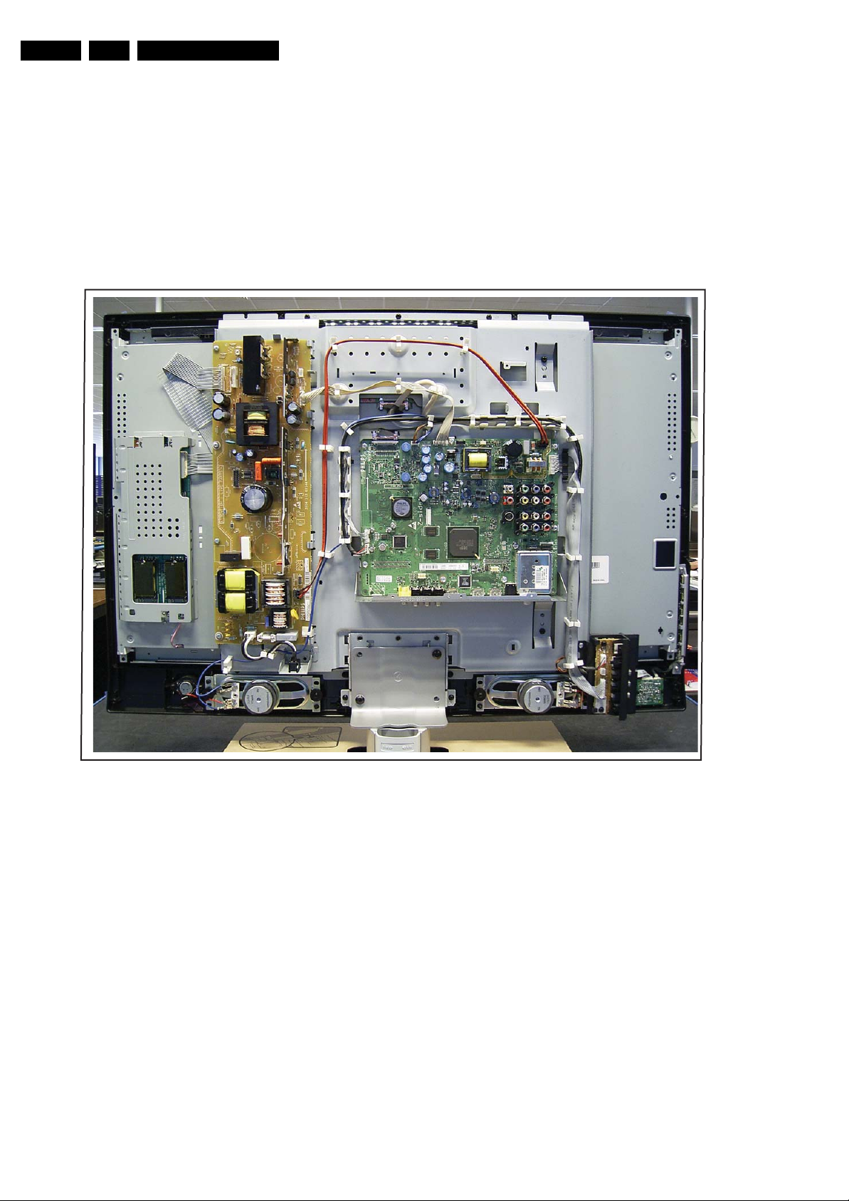
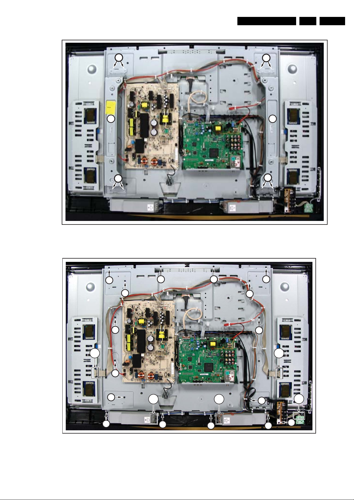
Figure 4-1 Cable dressing 32" sets
H_16790_058.eps
220807

Mechanical Instructions
EN 9Q528.1A LA 4.
Figure 4-2 Cable dressing 42” ME7 styling sets
H_16790_058.eps
220807
Figure 4-3 Cable dressing 42" Aurea styling sets
H_16790_076.eps
111007

EN 10 Q528.1A LA4.
Mechanical Instructions
4.2 Service Positions
For easy servicing of this set, there are a few possibilities
created:
• The buffers from the packaging (see figure “Rear cover”).
• Foam bars (created for Service).
• Aluminium service stands (created for Service).
4.2.1 Foam Bars
1
Required for sets
1
42"
Figure 4-4 Cable dressing 47" sets
The foam bars (order code 3122 785 90580 for two pieces) can
be used for all types and sizes of Flat TVs. See figure “Foam
bars” for details. Sets with a display of 42" and larger, require
four foam bars [1]. Ensure that the foam bars are always
supporting the cabinet and never only the display.
Caution: Failure to follow these guidelines can seriously
damage the display!
By laying the TV face down on the (ESD protective) foam bars,
a stable situation is created to perform measurements and
alignments. By placing a mirror under the TV, you can monitor
the screen.
4.2.2 Aluminium Stands
H_16790_060.eps
220807
E_06532_018.eps
Figure 4-5 Foam bars
171106
E_06532_039.eps
290507
Figure 4-6 Aluminium stands
The MkII aluminium stands with order code 3122 785 90690,
can also be used to do measurements, alignments, and
duration tests. The stands can be (dis)mounted quick and easy
by means of sliding them in/out the “mushrooms”. The stands
are backwards compatible with the earlier models.

Mechanical Instructions
EN 11Q528.1A LA 4.
Important: For (older) FTV sets without these “mushrooms”, it
is obligatory to use the provided screws, otherwise it is possible
to damage the monitor inside!
4.3 Assy/Panel Removal ME7 styling
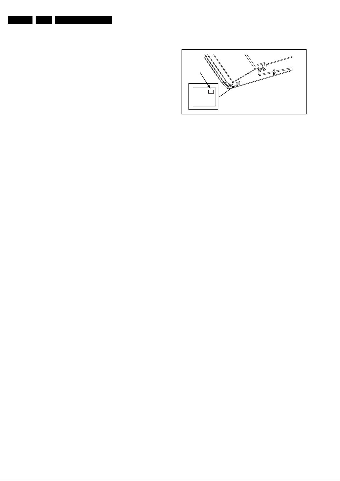
4.3.1 Rear Cover
Warning: Disconnect the mains power cord before you remove
the rear cover.
2
2 2 2
2
2
2
2
Warning: Most sets have additional doors located in the rear
cover. These are meant for disconnecting the flat cables to the
AmbiLight units in the rear cover, before the rear cover is
lifted from the set. The additional doors are not always
located at the same place for all sets, therefore the figures
below are only meant as indication.
It is mandatory to locate these additional doors first, open them,
and unplug connectors behind. Lifting the rear cover without
having done this, will result in damaging connectors inside!
Refer to next figures for details.
2
2
3
2
1
2
2
3
2
2 2
2
2
2
2
1. Remove the stand.
2. Remove the mushrooms [1].
3. Remove the screws [2].
4. Open the doors [3] on the back cover.
Refer to figures “Door Removal” for details.
4
Figure 4-7 Rear Cover Removal
1. Unplug connectors necessary for removing the backcover.
2
H_16770_081.eps
130707
Figure 4-9 Door Removal -2-
H_16770_084.eps
220307
Figure 4-8 Door Removal -1-
1. Unplug connector [4].
H_16770_082.eps
130707

EN 12 Q528.1A LA4.
4.3.2 Side I/O Board
Refer to figure “Side I/O Board” for details.
1. Unplug connectors [1].
2. Remove screw [2].
3. Push brackets [3], lift the PWB and slide it to the left out of
its casing.
When defective, replace the whole unit.
Mechanical Instructions
2
3
1
Figure 4-10 Side I/O Board
4.3.3 Keyboard Control Board
Refer to figures “Keyboard Control Board -1-” and “Keyboard
Control Board -2-” for details.
1. Remove the screws [1].
2. Lift the clamps [2].
3. Take the PWB out of its casing.
4. Unplug the connector [3] and remove the board.
When defective, replace the whole unit.
2
H_16770_085.eps
220307
Figure 4-12 Keyboard Control Board -2-
4.3.4 IR & LED Board
Refer to figure “IR & LED Board” for details.
1. Release clip [1], lift the board and take it out.
2. Unplug connector [2].
When defective, replace the whole unit.
3
H_16770_087.eps
220307
2
1
1
Figure 4-11 Keyboard Control Board -1-
H_16770_086.eps
220307
Figure 4-13 IR & LED Board
4.3.5 Speakers
Refer to figure “Speakers” for details.
1. Unplug connectors [1].
2. Remove screws [2].
H_16770_088.eps
220307

Mechanical Instructions
During re-assembly, refer to figure “Cable dressing 47" sets”
earlier in this chapter for the correct cable dressing!
EN 13Q528.1A LA 4.
1
1
2
1
Figure 4-14 Speakers
4.3.6 Display Supply Panel - 42" sets
Refer to figure “Display Supply Panel - 42" sets” for details.
1. Remove the fixation screws [1].
2. Unplug connectors [2].
3. Take the board out.
During re-assembly, refer to figure “Cable dressing 42" sets”
earlier in this chapter for the correct cable dressing!
1
H_16770_089.eps
130707
1
1
1
2
1
2
2
1
1
2
1
H_16770_090.eps
220307
1
1
1
1
Figure 4-15 Display Supply Panel - 42" sets
2
1
2
1
1
2
2
H_16770_091.eps
220307
Figure 4-16 Display Supply Panel - 47"sets
4.3.8 Dynamic Frame Insertion panel (DFI)
Refer to next figures for details.
1. Unplug the LVDS connectors [1].
Caution: be careful, as these are very fragile connectors!
2. Unplug the other connectors [2].
3. Remove the screws [3].
The DFI panel can now be taken out of the set.
3
2
1
3
3
3
3
3
4.3.7 Display Supply Panel - 47" and 52" sets
Refer to figure “Display Supply Panel - 47" sets” for details.
1. Remove the fixation screws [1].
2. Unplug connectors [2].
3. Take the board out.
Figure 4-17 DFI panel removal
H_16801_128.eps
310807

EN 14 Q528.1A LA4.
Mechanical Instructions
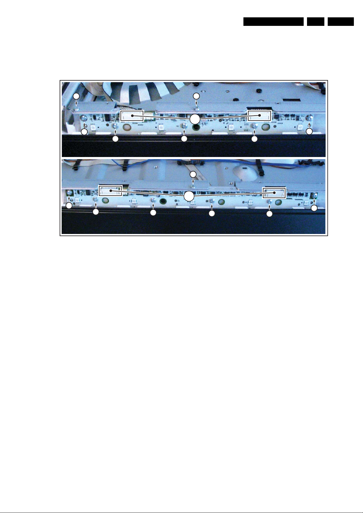
4.3.9 Small Signal Board (SSB)
Caution: it is mandatory to remount all different screws at their
original position during re-assembly. Failure to do so may result
in damaging the SSB.
Refer to figures “Small Signal Board -1-” and “Small Signal
Board -2-” for details.
1. Remove the tapping screws [1].
2. Unplug the connectors [2].
3. Unplug the LVDS connector [3]. Caution: be careful, as
this is a very fragile connector!
4. Remove the parker screws [4].
5. Remove the tapping screws [5].
6. Carefully lift the SSB at the top and take it out of the set.
1
1
3
2
1
2
1
1
4.3.10 AmbiLight Unit
The AmbiLight Units are located in the back cover. Refer to
figure “AmbiLight Unit” for details.
1. Remove the screws [1].
2. Unplug the connectors [2].
3. Slide the unit sideways and take it out of the backcover.
When defective, replace the whole unit.
1
1
2
1
2
3
1
1
Figure 4-18 Small Signal Board -1-
4 4 4 5 5
Figure 4-19 Small Signal Board -2-
H_16770_092.eps
220307
H_16770_093.eps
130707
1
Figure 4-20 AmbiLight Unit
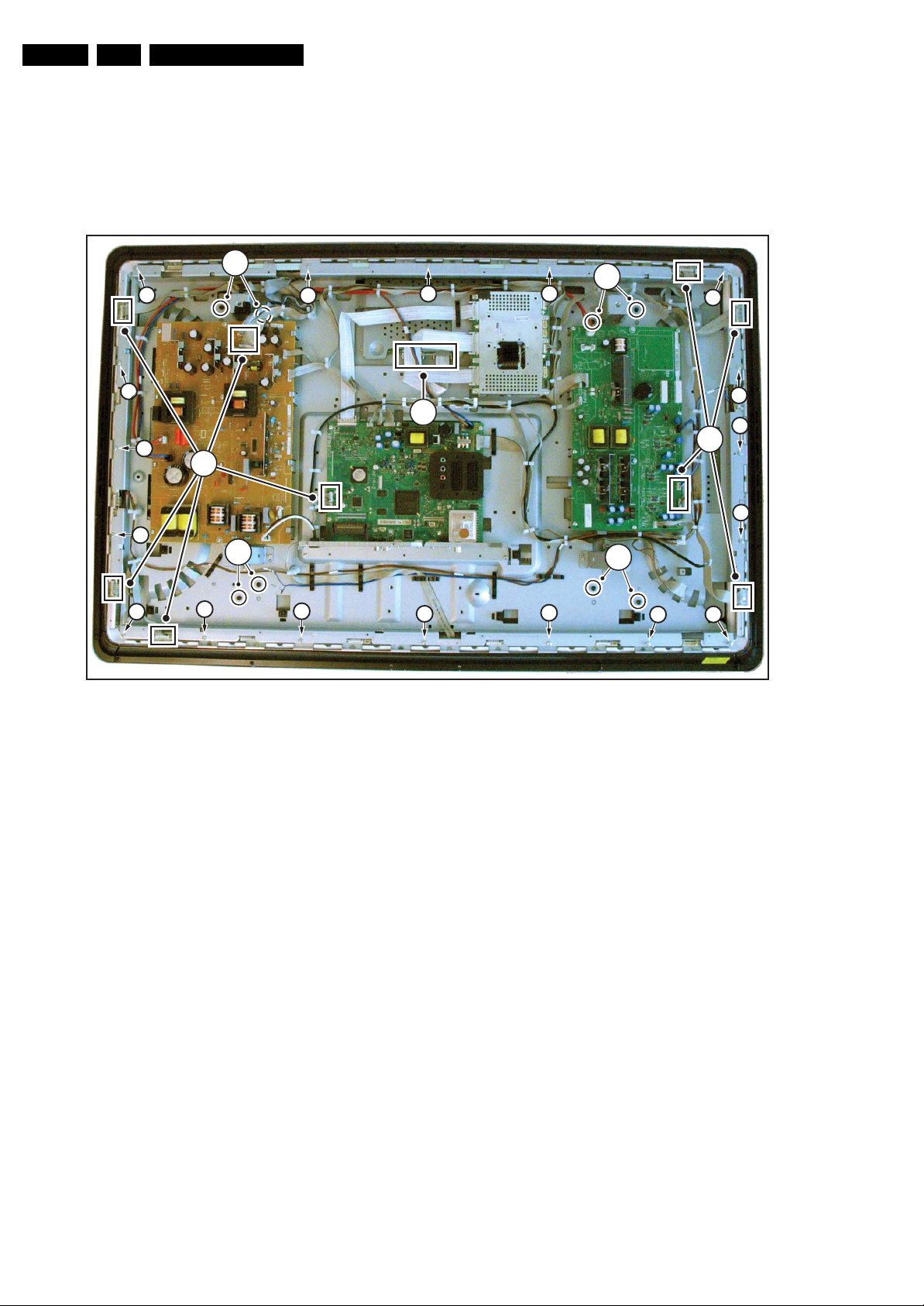
4.3.11 LCD Panel
Refer to figures “LCD Panel -1-” and “LCD Panel -2-” for details.
1. Remove the vertical brackets [1] by removing the screws
[2].
1. Unplug the connectors [3].
2. Unplug the LVDS connector [4] from the LCD panel.
Important: Be careful, as this is a very fragile connector!
3. Unplug the connectors [5] from the speakers.
4. Remove fixation screw [6] from the side I/O panel.
5. Unplug connector from LED I/R panel as earlier described
[7].
6. Remove fixation screws [8] and lift the complete central
sub-frame [6] from the set.
7. Lift the central sub-frame from the set. Refer to figure
Central Sub-frame lift for details.
8. Lift the LCD panel from the front cabinet.
H_16770_094.eps
240707
Mechanical Instructions
EN 15Q528.1A LA 4.
2
2
11
2
2
H_16770_095.eps
130707
Figure 4-21 LCD Panel -1-
8
8
8
3 3
8 8 8
8
8
8
8
5
5
8
7
8
8
Figure 4-22 LCD Panel -2-
88
6
H_16770_096.eps
120707

EN 16 Q528.1A LA4.
Mechanical Instructions
Figure 4-23 Central Sub-frame
H_16770_097.eps
130707

Mechanical Instructions
EN 17Q528.1A LA 4.
4.4 Assy/Panel Removal Aurea Styling
Note: Pictures in this section are taken from European chassis
(only difference: use of another Small Signal Board).
4.4.1 Rear Cover
Warning: Disconnect the mains power cord before you remove
the rear cover.
Note: it is not necessary to remove the stand while removing
the rear cover.
2
2
1
2
2
2
2
Refer to next figures for details.
2 22
2
2
1
2
2
2
2
2
2
2 2
2
2
2
2
2
2
2
1. Place the TV set upside down on a table top, using the
foam bars (see part “Foam Bars”).
Caution: do not put pressure on the display, but let the
monitor lean on the cabinet!
2. Remove the mushrooms [1].
3. Remove the screws [2].
4. Lift the rear cover from the TV.
4.4.2 Side I/O Board
Refer to next figure for details.
1. Unplug both connectors [1] and remove the screw [2].
2. Lift out the whole unit.
When defective, replace the whole unit.
Figure 4-24 Rear Cover Removal
H_16801_103.eps
2
270807
1
Figure 4-25 Side I/O Board
H_16801_104.eps
270807

EN 18 Q528.1A LA4.
4.4.3 Stand Removal
Refer to next figures for details.
1. Place the set in the service position.
2. Remove the screws [1] and pull the stand downwards out
of its support.
3. Remove the screws [2] and lift out the support.
Mechanical Instructions
2
H_16801_106.eps
270807
1
Figure 4-26 Stand removal [1/2]
1
H_16801_105.eps
270807
Figure 4-27 Stand removal [1/2]
4.4.4 Ambilight Reflector and Low-range Speaker removal
Caution: The speakers should never be connected or
disconnected when the set is playing! This can damage the
amplifiers on the SSB.
Refer to next figure for details.
1. Remove the screws[1].
2. Lift the whole reflector from the set.
3. Remove the connectors [2] from the low-range speakers.
4. Remove the screws [3] from the low-range speakers and
lift them from the sub-frame. When defective, replace the
whole unit.
1
1
1
3
Figure 4-28 Ambilight Reflector and Low-range Speaker removal
2 2
3
H_16801_107.eps
280807
Mechanical Instructions
EN 19Q528.1A LA 4.
4.4.5 Ambilight LED Panel Removal
The set contains two different Ambilight LED panels. A four
LED and a five LED version. Removal is similar for both types.
Refer to next figure for details.
2
3
3
3
3
1. Unplug the connectors [1].
2. Remove the screws [2] and [3].
3. Pull the panel forward and lift them from the sub-frame.
When defective, replace the whole unit.
2
1
3
3
3
2
1
3
3
3
3
Figure 4-29 Ambilight LED panel removal
H_16801_108.eps
280807
EN 20 Q528.1A LA4.
Mechanical Instructions
4.4.6 Subframe Removal
Before the Subframe can be removed, please remove the
Ambilight Reflector and Low-range Speaker as described
earlier.
For replacing the Keyboard Control Board, the IR & LED board,
the Tweeters, and the LCD panel, the Subframe and Rim have
to be removed first.
4
3
3
3
3
2
3
4
Refer to next figure for details.
1. Do NOT forget to unplug the LVDS connector [1] from the
SSB. Important: Be careful, as this is a very fragile
connector!
2. Unplug the connectors[2].
3. Remove the screws [3] and [4].
4. Now lift the subframe from the set.
3 3
1
4
3
3
3
2
3
4
3
3
3
Figure 4-30 Subframe removal
3
3
3
3
H_16801_109.eps
280807

Mechanical Instructions
EN 21Q528.1A LA 4.
4.4.7 Rim removal
For replacing the Keyboard Control Board, the IR & LED board,
the Tweeters and the LCD panel, the Subframe and Rim have
to be removed first.
Refer to next figure for details.
1. Remove the screws [1].
2. Lift the rim from the set.
1
4.4.8 IR & LED Board
For replacing the IR & LED Board, the Subframe and the Rim
have to be removed first. Please refer to the sections Subframe
removal and Rim removal.
Refer to next figure for details.
1. Unplug connectors [1].
2. Remove the screws [2].
3. Lift the board and take it out of the set.
When defective, replace the whole unit.
1
2
H_16801_111.eps
300807
Figure 4-31 Rim removal
H_16801_112.eps
300807
Figure 4-32 IR & LED Board
4.4.9 Keyboard Control Board
For replacing the Keyboard Control Board, the Subframe and
the Rim have to be removed first. Please refer to the sections
Subframe removal and Rim removal.
Refer to next figure for details.
1. Remove the screws [1].
2. Lift the unit from the set in the shown direction.
3. Unplug the connector and remove the board.
4. Lift the clamps [2].
2
1
Figure 4-33 Keyboard Control Board
H_16801_110.eps
300807

EN 22 Q528.1A LA4.
4.4.10 Tweeters removal
Caution: The tweeters should never be connected or
disconnected when the set is playing! This can damage the
amplifiers on the Audio/Standby Board.
For replacing the IR & LED Board, the Subframe and the Rim
have to be removed first. Please refer to the sections Subframe
removal and Rim removal.
Refer to next figure for details.
1. Unplug connector [1].
2. Remove screws [2].
3. Take the tweeters out together with their casing.
When defective, replace the whole unit.
Mechanical Instructions
2
1
4.4.11 LCD Panel
For replacing the LCD Panel, the Subframe has to be removed
first. Please refer to the section Subframe removal.
Refer to next figure for details.
1
Figure 4-34 Tweeters removal
1. Lift the LCD panel from the front cabinet.
When defective, replace the whole unit.
1
H_16801_113.eps
300807
1
4.4.12 Small Signal Board (SSB)
Caution: it is mandatory to remount all different screws at their
Figure 4-35 LCD Panel
1
H_16801_114.eps
300807
original position during re-assembly. Failure to do so may result
in damaging the SSB.
Refer to next figures for details.

1. Unplug the LVDS connector [1].
Caution: be careful, as this is a very fragile connector!
2. Unplug the connectors [2].
3. Remove the screws [3].
4. Remove the parker screws [4].
5. Remove the tapping screws [5].
The SSB can now be taken out of the set.
3
1 2
3
Mechanical Instructions
3
2
EN 23Q528.1A LA 4.
2
2
2
1
2
2
3
3
Figure 4-36 Small Signal Board removal [1/2]
Figure 4-37 Small Signal Board removal [2/2]
4.4.13 Power Supply Unit (PSU)
Refer to next figure for details.
1. Unplug the connectors [1].
2. Remove the screws [2].
The PSU can now be taken out of the set.
3
3
1
2
2
H_16801_126.eps
030907
2
1
2
44
555
H_16800_120.eps
240707
Figure 4-38 PSU panel removal
4.4.14 Dynamic Frame Insertion panel (DFI)
Refer to next figures for details.
1. Unplug the LVDS connectors [1].
Caution: be careful, as these are very fragile connectors!
2. Unplug the other connectors [2].
3. Remove the screws [3].
The DFI panel can now be taken out of the set.
H_16801_127.eps
310807
3
1
3
3
Figure 4-39 DFI panel removal
3
2
3
3
H_16801_128.eps
310807

EN 24 Q528.1A LA4.
4.4.15 Audio and Ambilight supply panel
Refer to next figures for details.
1. Unplug the connectors [1].
2. Remove the screws [2].
The Audio and Ambilight supply panel can now be taken out of
the set.
Mechanical Instructions
2
2
1
2
2
1
2
2
Figure 4-40 Audio and Ambilight supply panel removal
4.5 Set Re-assembly
2
2
2
H_16801_129.eps
310807
To re-assemble the whole set, execute all processes in reverse
order.
Notes:
• While re-assembling, make sure that all cables are placed
and connected in their original position. Only refer to
figures “Cable dressing” at the beginning of this
chapter!
• Pay special attention not to damage the EMC foams on the
SSB shields. Ensure that EMC foams are mounted
correctly.
Service Modes, Error Codes, and Fault Finding
5. Service Modes, Error Codes, and Fault Finding
EN 25Q528.1A LA 5.
Index of this chapter:
5.1 Test Points
5.2 Service Modes
5.3 Stepwise Start-up
5.4 Service Tools
5.5 Error Codes
5.6 The Blinking LED Procedure
5.7 Protections
5.8 Fault Finding and Repair Tips
5.9 Software Upgrading
5.1 Test Points
As most signals are digital, it will be difficult to measure
waveforms with a standard oscilloscope. However, several key
ICs are capable of generating test patterns, which can be
controlled via ComPair. In this way it is possible to determine
which part is defective.
Perform measurements under the following conditions:
• Service Default Mode.
• Video: Colour bar signal.
• Audio: 3 kHz left, 1 kHz right.
5.2 Service Modes
Service Default mode (SDM) and Service Alignment Mode
(SAM) offers several features for the service technician, while
the Customer Service Mode (CSM) is used for communication
between the call centre and the customer.
This chassis also offers the option of using ComPair, a
hardware interface between a computer and the TV chassis. It
offers the abilities of structured troubleshooting, error code
reading, and software version read-out for all chassis.
(see also paragraph “ComPair”).
– Picture mute (blue mute or black mute).
– Automatic volume levelling (AVL).
– Skip/blank of non-favourite pre-sets.
How to Activate SDM
For this chassis there are two kinds of SDM: an analogue SDM
and a digital SDM. Tuning will happen according table “SDM
Default Settings”.
• Analogue SDM: use the standard RC-transmitter and key
in the code “062596”, directly followed by the “MENU”
button.
Note: It is possible that, together with the SDM, the main
menu will appear. To switch it “off”, push the “MENU”
button again.
• Digital SDM: use the standard RC-transmitter and key in
the code “062593”, directly followed by the “MENU” button.
Note: It is possible that, together with the SDM, the main
menu will appear. To switch it “off”, push the “MENU”
button again.
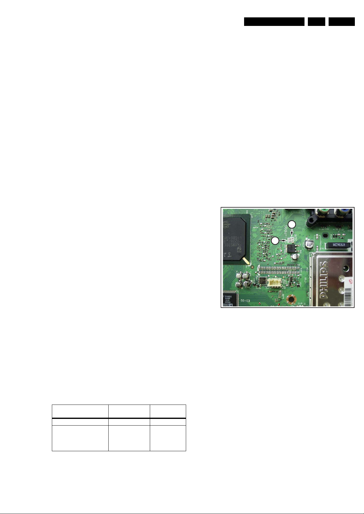
• Analogue SDM can also be activated by shorting for a
moment the two solder pads [1] (see figure “Service mode
pads”) on the SSB, with the indication “SDM”. Activation
can be performed in all modes, except when the set has a
problem with the Stand-by Processor.
1
2
5.2.1 Service Default Mode (SDM)
Purpose
• To create a pre-defined setting, to get the same
measurement results as given in this manual.
• To override SW protections detected by stand-by
processor and make the TV start up to the step just before
protection (a sort of automatic stepwise start up). See
paragraph “Stepwise Start Up”.
• To override SW protections detected by MIPS. See also
paragraph “Error codes”.
• To start the blinking LED procedure (not valid for
protections detected by standby software).
Specifications
Table 5-1 SDM default settings
Region Freq. (MHz)
Europe, AP(PAL/Multi) 475.25 PAL B/G
Europe, AP DVB-T 546.00 PID
Video: 0B 06 PID
PCR: 0B 06 PID
Audio: 0B 07
• All picture settings at 50% (brightness, colour, contrast).
• All sound settings at 50%, except volume at 25%.
• All service-unfriendly modes (if present) are disabled, like:
– (Sleep) timer.
– Child/parental lock.
Default
system
DVB-T
Figure 5-1 Service mode pads
After activating this mode, “SDM” will appear in the upper right
corner of the screen (if you have picture).
How to Navigate
When you press the “MENU” button on the RC transmitter, the
set will toggle between the SDM and the normal user menu
(with the SDM mode still active in the background).
How to Exit SDM
Use one of the following methods:
• Switch the set to STAND-BY via the RC-transmitter.
• Via a standard customer RC-transmitter: key in “00”sequence.
5.2.2 Service Alignment Mode (SAM)
Purpose
• To perform (software) alignments.
• To change option settings.
• To easily identify the used software version.
• To view operation hours.
• To display (or clear) the error code buffer.
H_16770_100.eps
130707
EN 26 Q528.1A LA5.
Service Modes, Error Codes, and Fault Finding
How to Activate SAM
Via a standard RC transmitter: key in the code “062596”
directly followed by the “INFO” button. After activating SAM
with this method a service warning will appear on the screen,
you can continue by pressing the red button on the RC.
Contents of SAM:
• Hardware Info.
– A. SW Version. Displays the software version of the
main software (example: Q581E-1.2.3.4 =
AAAAB_X.Y.W.Z).
• AAAA= the chassis name.
• B= the region: A= AP, E= EU, L= LatAm, U = US.
For AP sets it is possible that the Europe software
version is used.
• X.Y.W.Z= the software version, where X is the
main version number (different numbers are not
compatible with one another) and Y.W.Z is the sub
version number (a higher number is always
compatible with a lower number).
– B. SBY PROC Version. Displays the software version
of the stand-by processor.
– C. Production Code. Displays the production code of
the TV, this is the serial number as printed on the back
of the TV set. Note that if an NVM is replaced or is
initialized after corruption, this production code has to
be re-written to NVM. ComPair will foresee in a
possibility to do this.
• Operation Hours. Displays the accumulated total of
operation hours (not the stand-by hours). Every time the
TV is switched “on/off”, 0.5 hours is added to this number.
• Errors (followed by maximal 10 errors). The most recent
error is displayed at the upper left (for an error explanation
see paragraph “Error Codes”).
• Reset Error Buffer. When you press “cursor right” (or the
“OK button) and then the “OK” button, the error buffer is
reset.
• Alignments. This will activate the “ALIGNMENTS” submenu.
• Dealer Options. Extra features for the dealers.
• Options. Extra features for Service. For more info
regarding option codes, see chapter 8 “Alignments”.
Note that if you change the option code numbers, you have
to confirm your changes with the “OK” button before you
store the options. Otherwise you will loose your changes.
• Initialize NVM. The moment the processor recognizes a
corrupted NVM, the “initialize NVM” line will be highlighted.
Now, you can do two things (dependent of the service
instructions at that moment):
– Save the content of the NVM via ComPair for
development analysis, before initializing. This will give
the Service department an extra possibility for
diagnosis (e.g. when Development asks for this).
– Initialize the NVM.
Note: When you have a corrupted NVM, or you have replaced
the NVM, there is a high possibility that you will not have picture
anymore because your display code is not correct. So, before
you can initialize your NVM via the SAM, you need to have a
picture and therefore you need the correct display option. Refer
to chapter 8 for details. To adapt this option, you can use
ComPair (the correct HEX values for the options can be found
in chapter 8 “Alignments”) or a method via a standard RC
(described below).
Changing the display option via a standard RC: Key in the
code “062598” directly followed by the “MENU” button and
“XXX”, where XXX is the 3 digit decimal display code (see table
“Option code overview” in chapter 8 “Alignments”, or sticker on
the side/bottom of the cabinet). Make sure to key in all three
digits, also the leading zero’s. If the above action is successful,
the front LED will go out as an indication that the RC sequence
was correct. After the display option is changed in the NVM, the
TV will go to the Stand-by mode. If the NVM was corrupted or
empty before this action, it will be initialized first (loaded with
default values). This initializing can take up to 20 seconds.
Display Option
Code
39mm
040
PHILIPS
MODEL:
32PF9968/10
27mm
PROD.SERIAL NO:
AG 1A0620 000001
(CTN Sticker)
E_06532_038.eps
290107
Figure 5-2 Location of Display Option Code sticker
Restore the correct Lava/Lounge mode (only for Aurea):
These settings are done automatically when the NVM is
initialized (and loaded with default values).
• Store. All options and alignments are stored when
pressing “cursor right” (or the “OK” button) and then the
“OK”-button.
• SW Maintenance.
– SW Events. Not useful for Service purposes. In case
of specific software problems, the development
department can ask for this info.
– HW Events. Not useful for Service purposes. In case
of specific software problems, the development
department can ask for this info.
• Test settings. For development purposes only.
• Upload to USB. To upload several settings from the TV to
a USB stick, which is connected to the Side I/O. The items
are “Channel list”, “Personal settings”, “Option codes”,
“Display-related alignments” and “History list”. First you
have to create a directory “repair” in the root of the USB
stick.To upload the settings you have to select each item
separately, press “cursor right” (or the “OK button), confirm
with “OK” and wait until “Done” appears. In case the
download to the USB stick was not successful “Failure” will
appear. In this case, check if the USB stick is connected
properly and if the directory “repair” is present in the root of
the USB stick. Now the settings are stored onto your USB
stick and can be used to download onto another TV or
other SSB. Uploading is of course only possible if the
software is running and if you have a picture. This method
is created to be able to save the customer’s TV settings
and to store them into another SSB.
• Download from USB. To download several settings from
the USB stick to the TV. Same way of working as with
uploading. To make sure that the download of the channel
list from USB to the TV is executed properly, it is necessary
to restart the TV and tune to a valid preset if necessary.
Note: The “History list item” can not be downloaded from
USB to the TV. This is a “read-only” item. In case of specific
problems, the development department can ask for this
info.
How to Navigate
• In SAM, you can select the menu items with the “CURSOR
UP/DOWN” key on the RC-transmitter. The selected item
will be highlighted. When not all menu items fit on the
screen, move the “CURSOR UP/DOWN” key to display the
next/previous menu items.
• With the “CURSOR LEFT/RIGHT” keys, it is possible to:
– (De) activate the selected menu item.
– (De) activate the selected sub menu.
• With the “OK” key, it is possible to activate the selected
action.
How to Exit SAM
Use one of the following methods:
• Press the “MENU” button on the RC-transmitter.

Service Modes, Error Codes, and Fault Finding
EN 27Q528.1A LA 5.
• Switch the set to STAND-BY via the RC-transmitter.
5.2.3 Customer Service Mode (CSM)
Purpose
When a customer is having problems with his TV-set, he can
call his dealer or the Customer Helpdesk. The service
technician can then ask the customer to activate the CSM, in
order to identify the status of the set. Now, the service
technician can judge the severity of the complaint. In many
cases, he can advise the customer how to solve the problem,
or he can decide if it is necessary to visit the customer.
The CSM is a read only mode; therefore, modifications in this
mode are not possible.
When in this chassis CSM is activated, a colour bar test pattern
will be visible for 5 seconds. This test pattern is generated by
the Pacific3. So if you see this test pattern you can determine
that the back end video chain (Pacific3, LVDS, and display) of
the SSB is working. In case of a set with DFI panel, an extra
test picture is generated. So you will see the Pacific3 test
picture for 3 seconds and then the DFI EPLD test picture for
another 3 seconds. With this extra test picture you can
determine if the DFI board is working properly.
Also new in this chassis: when you activate CSM and there is
a USB stick connected to the TV, the software will dump the
complete CSM content to the USB stick. The file (Csm.txt) will
be saved in the root of your USB stick. This info can be handy
if you do not have picture.
Another new item in this chassis is when CSM is activated, the
complete error-buffer content will be shown via the blinking
LED procedure.
How to Activate CSM
Key in the code “123654” via the standard RC transmitter.
Note: Activation of the CSM is only possible if there is no (user)
menu on the screen!
How to Navigate
By means of the “CURSOR-DOWN/UP” knob on the RCtransmitter, you can navigate through the menus.
Contents of CSM
• Set Type. This information is very helpful for a helpdesk/
workshop as reference for further diagnosis. In this way, it
is not necessary for the customer to look at the rear of the
TV-set. Note that if an NVM is replaced or is initialized after
corruption, this set type has to be re-written to NVM.
ComPair will foresee in a possibility to do this.
• Production Code. Displays the production code (the serial
number) of the TV. Note that if an NVM is replaced or is
initialized after corruption, this production code has to be
re-written to NVM. ComPair will foresee a in possibility to
do this.
• Code 1. Gives the last five errors of the error buffer. As
soon as the built-in diagnose software has detected an
error, the buffer is adapted. The last occurred error is
displayed on the leftmost position. Each error code is
displayed as a 2-digit number. When less than 10 errors
occur, the rest of the buffer is empty (00). See also
paragraph “Error Codes” for a description.
• Code 2. Gives the first five errors of the error buffer. See
also paragraph “Error Codes” for a description.
• Options 1. Gives the option codes of option group 1 as set
in SAM (Service Alignment Mode).
• Options 2. Gives the option codes of option group 2 as set
in SAM (Service Alignment Mode).
• 12NC SSB. Gives an identification of the SSB as stored in
NVM. Note that if an NVM is replaced or is initialized after
corruption, this identification number has to be re-written to
NVM. ComPair will foresee in a possibility to do this. This
identification number consists of 14 characters and is built
up as follows:
- Seven last characters of the 12NC of the SSB itself.
- the serial number of the SSB, which consists of seven
digits. Both can be found on a sticker on the PWB of the
SSB itself. The format of the identification number is then
as follows: <last seven characters of 12NC of SSB><serial
number of SSB> (total fourteen characters).
• Installed date. Indicates the date of the first installation of
the TV. This date is acquired via time extraction.
• Digital Natural Motion. Gives the status of the Digital
Natural Motion setting as set by the customer. Remark: a
customer can choose between “OFF”, “MINIMUM” and
“MAXIMUM”, but in CSM this item will only show “OFF” or
“ON” (“ON” in case the customer has chosen “MINIMUM”
or “MAXIMUM”)
• Pixel Plus. Gives the last status of the Perfect Pixel HD
setting, as set by the customer. Possible values are “ON”
and “OFF”. See DFU on how to change this item.
• DNR. Gives the last status of the Noise reduction setting,
as set by the customer. Possible values are “OFF”,
“MINIMUM”, “MEDIUM” and “MAXIMUM”. See DFU on
how to change this item.
• Noise Figure. Gives an indication of the signal quality for
the selected transmitter. Possible values are “BAD”,
“AVERAGE”, “GOOD” and “DIGITAL”. In case of a digital
channel, this item will never indicate: “BAD”, “GOOD” or
“AVERAGE” but only displays “DIGITAL”.
• 12NC Display. Shows the 12NC of the display.
• Headphone Volume. Gives the last status of the
headphone volume, as set by the customer. The value can
vary from 0 (volume is minimum) to 100 (volume is
maximum). See DFU on how to change this item.
• Surround Mode. Indicates the by the customer selected
sound mode (or automatically chosen mode). Possible
values are “STEREO” and “VIRTUAL DOLBY
SURROUND”. It can also have been selected
automatically by signalling bits (internal software). See
DFU on how to change this item.
• AVL. Indicates the last status of AVL (Automatic Volume
Level) as set by the customer: See DFU on how to change
this item.
• Delta Volume. Indicates the last status of the delta volume
for the selected preset as set by the customer: from “-12”
to “+12”. See DFU on how to change this item.
• Volume. Indicates the last status of the volume for the
selected preset as set by the customer: from “0” to “100”.
See DFU on how to change this item.
• Balance. Indicates the last status of the balance for the
selected preset as set by the customer: from “-10” to “+10”.
See DFU on how to change this item.
• Preset Lock. Indicates if the selected preset has a child
lock: “LOCKED” or “UNLOCKED”. See DFU on how to
change this item.
• Lock after. Indicates at what time the channel lock is set:
“OFF” or e.g. “18:45” (lock time). See DFU on how to
change this item.
• Parental rating lock. Indicates the “Parental rating” as set
by the customer. See DFU on how to change this item.
• Parental rating status. Indicates the “Parental rating” as
transmitted by the broadcaster (if applicable). If the
parental rating status is indicating a higher age then the
parental rating lock as set by the customer, you will need to
enter the child lock code.
• TV ratings lock. Only applicable for US.
• Movie ratings lock. Only applicable for US.
•
On timer. Indicates if the “On timer” is set “ON” or “OFF”
and when it is set to “ON”, also start time, start day and
program number is displayed. See DFU on how to change
this item.
• Location. Gives the last status of the location setting as
set via the installation menu. Possible values are “SHOP”
and “HOME”. If the location is set to “SHOP”, several
settings are fixed. So for a customer location must be set
to “HOME”. Can be changed via the installation menu (see
also DFU).

EN 28 Q528.1A LA5.
• HDMI key validity. Indicates if the HDMI keys (or HDCP
keys) are valid or not. In case these keys are not valid and
the customer wants to make use of the HDMI functionality,
the SSB has to be replaced.
• Tuner frequency. Indicates the frequency the transmitter
is tuned to.
• TV System. Gives information about the video system of
the selected transmitter. In case a DVBT signal is received
this item will also show ATSC.
– BG: PAL BG signal received
– DK: PAL DK signal received
– L/La: SECAM L/La signal received
– I: PAL I signal received
– M: NTSC M signal received
– ATSC: ATSC signal received
– DVB: DVBT signal received
• 12NC one zip SW. Displays the 12NC number of the onezip file as it is used for programming software in production.
In this one-zip file all below software versions can be found.
• Initial main SW. Displays the main software version which
was initially loaded by the factory.
• Current main SW. Displays the built-in main software
version. In case of field problems related to software,
software can be upgraded. As this software is consumer
upgradeable, it will also be published on the Internet.
Example: Q581E_1.2.3.4.
• Flash utilities SW. Displays the software version of the
software which contains all necessary components of the
download application. To program this software, EJTAG
tooling is needed. Example: Q581E_1.2.3.4.
• Standby SW. Displays the built-in stand-by processor
software version. Upgrading this software will be possible
via ComPair or via USB (see chapter Software upgrade).
Example: STDBY_3.0.1.2.
• MOP SW. Only applicable for US. At the time of release of
this manual, there was still a problem with this item, and
some rubbish was displayed. Ignore this.
• Pacific 3 Flash SW. Displays the Pacific 3 software
version.
• NVM version. Displays the NVM version as programmed
by factory.
• Display parameters. for development purposes only.
• Private PQ parameters. for development purposes only.
• Public PQ parameters. for development purposes only.
• Ambilight parameters. for development purposes only.
• Acoustics parameters. for development purposes only.
• DFI software (if applicable). Displays the DFI EPLD
software.
• DFI ambilight software (if applicable). Displays the DFI
ambilight EPLD software.
Service Modes, Error Codes, and Fault Finding
How to Exit CSM
Press “MENU” on the RC-transmitter.

Service Modes, Error Codes, and Fault Finding
EN 29Q528.1A LA 5.
5.3 Stepwise Start-up
There are two possible situations: one for protections detected
by the stand-by software and one for protections detected by
the main software.
When the TV is in a protection state due to an error detected by
stand-by software (and thus blinking an error) and SDM is
activated via short-circuiting the pins on the SSB, the TV starts
up until it reaches the situation just before protection. So, this
is a kind of automatic stepwise start-up. In combination with the
start-up diagrams below, you can see which supplies are
present at a certain moment. Important to know is, that if e.g.
the 3V3 detection fails (and thus error 8 is blinking) and the TV
is restarted via SDM, the Stand-by Processor will enable the
3V3, but will not go to protection now. The TV will stay in this
situation until it is reset (Mains/AC Power supply interrupted).
Caution: in case the start up in this mode with a faulty FET
7U01 is done, you can destroy all IC’s supplied by the +3V3,
Mains
off
Off
Mains
on
due to overvoltage. It is recommended to measure first the FET
7U01 on short-circuit before activating SDM via the service
pads.
When the TV is in protection state due to an error detected by
main software (MIPS protection) and SDM is activated via
short-cutting the service pads on the SSB, the TV starts up and
ignores the error.
In this chassis, only error “63” (power-ok) is a MIPS protection
and already displays the failure via blinking LED.
The abbreviations “SP” and “MP” in the figures stand for:
• SP: protection or error detected by the Stand-by
Processor.
• MP: protection or error detected by the MIPS Main
Processor.
- WakeUp requested
- Acquisition needed
- No data Acquisition
required
- tact SW pushed
- last status is hibernate
after mains ON
Tact switch
pushed
- Tact switch Pushed
- last status is hibernate
after mains ON
St by
Hibernate
On
In US region, hibernate state and tact switch are not available.
Here the local keyboard tact switch acts as standby button.
Figure 5-3 Transition diagram
Semi
St by
GoToProtection
WakeUp
requested
- St by requested
- tact SW pushed
WakeUp
requested
(SDM)
Protection
Active
GoToProtection
H_16770_116.eps
270307
EN 30 Q528.1A LA5.
Service Modes, Error Codes, and Fault Finding
Off/Stby to Semi
action holder: MIPS
action holder: St-by
autonomous action
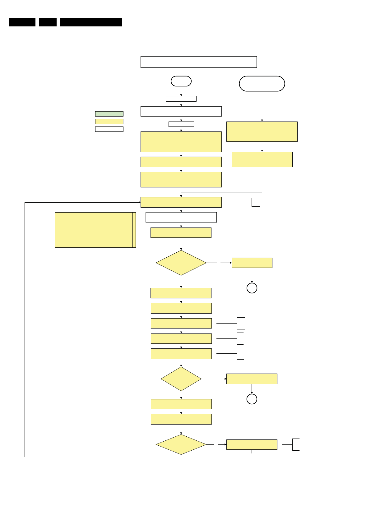
The a vailability of the supplies is checked through detect
signals going to the st-by µP. These signals are available
for +12V and +5V (combined as AND function, called
detect-5V-12V) and for +1V2 and +3V3 (combined as
AND function, called detect-1V2-2V5-3V). A low to high
transition of the signals should occur within a certain time
after toggling the standby line. If an observer is detected
before the time-out elapses, of course, the process
should continue in order to minimize start up time.
Off
Mains is app lied
Standby Supply starts running.
All standby supply voltages become available .
st-b y µP resets
All I/O lines have a High default state:
- Switch PNX85xx in reset (active LOW).
- NVM power line is high, no NVM communication possible.
Initialise I/O pins of the st-by µP, start keyboard scanning, RC
because o f the stby µP r eset in an FH P set) which w ill start the
Switch ON Platform and display supply by switching LOW the
- Keep the Audio-reset high.
detection. Wake up reasons are off.
PDPGO line is high (either HW wise in a non FHP set or
FHP PDP.
POD- MODE and t he ON-MODE I /O lines.
+5V, and +12V are switched on
Wait 50ms and the n start pollin g the detect -
5V-12V every 40ms.
detect-5V-12V received within
2900 ms after POD-mode I/O
line toggle?
Stand by or
Protection
If the protection state was left by short circuiting the
SDM pins, detection of a protection condition during
startup will stall the startup. Protection conditions in a
playing set will be ignor ed. Th e protect ion mode will
No
not be entered.
- Switch Audio-Reset high.
It is low in the standby mode if the standby
mode lasted longer than 10s.
Display su pply is switched on
through the ON-mode I/O line
“5V 12V supply” er ror
Yes
activat e +5V/+ 12V supply
detection algorithm. See CHS protections.
Enable the +1V2 supply (ENABLE-1V2 )
Wait 100ms
Enable the supply for
+1.8V and +3. 3V (ENABLE-3V3)
Start polling the detect-1V2-2V5-3V3
every 40ms
Detection
received within
250 ms after enable-3V3
toggle?
Yes
Activate supply detection algorithms for DC-
DC outputs
Wait 20ms
SUPPLY-F AULT I/O line
is High ?
SP
50ms is used in the Jaguar platform.
100ms is recommended by the
PNX85xx spec.
No separate enable is present
for the +1V8 supply in the
TV520.
Only one detect line is present
in the TV520: it detects +1V2
and +3V3
No
1V2 2V5 3V3 DCDC error
SP
No
Supply fault error
The supply fault line is an OR
function of DCDC, DCDC5050
and POD /CI supply sw itch.
H_16770_109a.eps
230707
Figure 5-4 “Off” to “Semi Stand-by” flowchart (part 1)

Service Modes, Error Codes, and Fault Finding
EN 31Q528.1A LA 5.
SUPPLY-F AULT I/O line
is High ?
No
Switch LOW the RESET-NVM_WP-NANDFLASH line. Add a 2ms delay before
trying to address the NVM to allow correct NVM initialization.
(pulling pin of the probe interface to
ground by inserting EJTAG probe)
No
No
Relea se AVC system r eset
Feed warm boot script
Yes
Enable the supply fault detection
algorithm
Set I²C slave address
of Standby µP to (A0h)
Detect EJTAG debug probe
EJTAG probe
connected ?
No
Cold boot?
Yes
Relea se AVC system r eset
Feed cold boot script
No
Supply fault error
SP
This will a llow access to NVM and
NAND FLASH and can not be done
earlier because the FLASH needs to
be in Write Protect as long as the
supplies are not available.
An EJTAG probe (e.g. WindPower ICE probe) can
be connected for Linux Kernel debugging purposes.
Yes
Relea se AVC system r eset
Feed initializing boot script
disable alive mechanism
The supply fault line is an OR
function of DCDC, DCDC5050
and POD/CI supply switch.
No
Code = 5
Switch AVC PNX8 5xx
in re set (act ive low)
Wait 10ms
Switch the NVM r eset
line HIGH .
Disable all supply related protections and
switch off the +2V5, +3V3 DC/DC converter.
Wait 5ms
Boot process of the PNX5050 also starts at this point. For full details,
see PNX5050 System Design document of Peter Deckmyn.
Bootscript ready
in 1250 ms?
Yes
Set I²C slave address
of Standby µP to (60h)
RPC start (comm. protocol)
No
Code = 53
Flash to Ram image
transfer succeeded
within 30s?
Yes
No
SW initializat ion
succeeded
within 20s?
Yes
Enable Alive check mechanism
MIPS reads the wake up reason
from standby µP.
In case of an LCD set, check t he
Power- OK display line
Wait until AVC starts to
commun icate
3-th try?
switch off the remaining DC/DC
converters
Switch POD-MODE and ON-MODE
I/O line high.
Power-ok display high ?
Yes
Reset t he Pacific by pulling LOW the Pacific
hardware reset line during 100ms.
No
Figure 5-5 “Off” to “Semi Stand-by” flowchart (part 2)
Log power-ok error and enter
protection
No
MP
H_16770_109b.eps
230707

EN 32 Q528.1A LA5.
Service Modes, Error Codes, and Fault Finding
switch off the remaining DC/DC
3-th try?
Yes
Blink Code as
error code
Switch POD -MODE and ON- MODE
SP
- Channeldecoder type TDA10060
cannot be reloaded without reset
of the channeldecoder.
- Channeldecoder type TDA10048
can be reloaded without reset.
conver ters
I/O line high.
Channel decoder
TDA 10048?
No
Third try? No
Power-ok display high ? No
Yes
Reset t he Pacific by pulling LOW the Pacific
hardware reset line during 100ms.
Relea se Pacific rese t
and wait 200ms
Ping the Pacific through I²C
Pacific acknowledges?
Yes
Init Pacific according use case:
- lvds or CMOS input and output
- panel config…
to be d iscussed with Stef an / SW if we w ill put this her e or in
the display excel overview of Stefan or in …..
Enable the Pacific output by sending the PanelConfig.PanelOn
to the Pacific in case of a DFI set
Start 4 seconds preheating timer in case of
an LPL scanning backlight LCD set.
Initialize audio accor ding FMS info rmation :
YesNo
Download firmware into the channel
decoder
Downloaded
successfu lly?
Log power-ok error and enter
protection
No
MP
Third Pacific boot retry?No
Yes
Log Pacific error
This is needed here because the Pacific has to
deliver an output clock towards the DFI. Otherwise
the DFI cannot deliver ambilight functionality in the
lampadaire mode. The presence of the DFI can be
determined via the display option.
Yes
Log channel decoder error
Yes
initialize tuner , Master IF and channel
decoder according FMS information
Initialize source selection according FMS
and CHS information
Wait until Cpipe delivers a stable output
Initialize video processing IC 's according FMS information:
- PNX5050 in /82
-scaler EPLD
initialize AutoTV by triggering CHS AutoTV Init interface
See appropriate CHS documents for further details.
Initialize Pacific or EPLD r elated Amb ilight
Do not enter semi-standby state in case of an LPL
scanning backlight LCD set before 4s preheating timer has
elapsed.
clock
Reset EPLD
Wait 100ms
Reset Pacific clock
settings (if applicable)
Initialize Ambilight with Lights off .
EPLD
and
Pacific
should
be reset
when a
stable
input
clock
become
s
available
at their
input.
Semi-Standby
Figure 5-6 “Off” to “Semi Stand-by” flowchart (part 3)
H_16770_109c.eps
110507

Service Modes, Error Codes, and Fault Finding
Semi Standby
Wait until previous on - state is left mor e than 2
seconds ago. (to prevent LCD display problems)
Assert RGB video blanking
and audio mute
EN 33Q528.1A LA 5.
action holder: AVC
action holder: St-by
autonomous action
Rewrite Pacific register 0x03 (output format) :
this command is sometimes not processed properly by the
Pacific at initialisation time , resending it here solves the issue .
Switch on the display by sending the
PanelConfig.PanelOn (I²C) command to the Pacific
wait 250ms (min. = 200ms)
Switch off the dimming backlight feature and
make sure PWM output is set to 100%
Switch on LCD backlight
The higher level requirement is that
audio and video should be demuted
without transient effects and that the
audio should be demuted maximum 1s
before or at the same time as the
unblanking of the video.
Initialize audio and video
processing IC's and functions
according needed use case.
Wait until valid and stable audio and video , corresponding to
the requested output is delivered by the AVC AND the
backlight PWM has been on for 1second.
Switch Audio-Reset low and wait 5ms
Release audio mute and wait 100ms before any other audio
handling is done (e.g. volume change)
Restore dimming backlight feature, PWM output and unblank
the video.
Active
Figure 5-7 “Semi Stand-by” to “Active” flowchart non DFI
H_16770_110.eps
290307

EN 34 Q528.1A LA5.
Service Modes, Error Codes, and Fault Finding
action holder: AVC
action holder: St-by
autonomous action
Semi Standby
Wait until previous on-state is left more than 2
seconds ago. (to prevent LCD display problems)
Assert RGB video blanking
and audio mute
Setting the display related timings of the DFI is not needed: The
display related timings are hardcoded in the DFI
Rewrite Pacific register 0x03 (output format) with TcuUpdate: this
command is sometimes not processed properly by the Pacific at
initialisation time, resending it here solves the issue.
Switch on the display panel and the lvds via
the OutputEnable DF I command
wait 250ms (min. = 200ms)
Switch off the dimming backlight feature and
make sure PWM output is set to 100%
Switch on LCD backlight
The higher level requirement is that
audio and video should be demuted
without transient effects and that the
audio should be demuted maximum 1s
before or at the same time as the
unblanking of the video.
Initialize audio and video
processing IC's and functions
accor ding neede d use case .
Wait until valid and stable audio and video, corr esponding to
the requested output is delivered by the AVC AND the
backlight PWM has been on for 1second.
Switch Audio-Reset low and wait 5ms
Release audio mute and wait 100ms before any other audio
handling is done (e.g. volume change)
Restore dimming backlight feature, PWM output and unblank
the video.
Active
Figure 5-8 “Semi Stand-by” to “Active” flowchart DFI
H_16770_111.eps
290307
Service Modes, Error Codes, and Fault Finding
EN 35Q528.1A LA 5.
Active
Mute all sound outputs via softmute
Wait 100ms
Set main amplifier mute (I/O: audio -mute)
Force ext audio outputs to ground
(I/O: audio reset)
And wait 5ms
switch off LCD backlight
action holder: AVC
action holder: St-by
autonomous action
Mute all video outputs
Wait 250ms (min. = 200ms)
Switch off the display by sending the
PanelConfig.PanelOff (I²C) command to the Pacific
switch off ambient light
Semi Standby
Figure 5-9 “Active” to “Semi Stand-by” flowchart (non-DFI)
H_16770_112.eps
260307
EN 36 Q528.1A LA5.
Service Modes, Error Codes, and Fault Finding
Active
Mute all sound outputs via softmute
Wait 100ms
Set main amplifier mute (I/O: audio-mute)
Force ext audio outputs to ground
(I/O: audio reset)
And wait 5ms
switch off LCD backlight
action holder: MIPS
action holder: St-by
autonomous action
Mute all video outputs
Wait 250ms (min. = 200ms)
Switch off the display by clearing the OutputEnable
control register in the DFI
switch off ambient light
Semi Standby
Figure 5-10 “Active” to “Semi Stand-by” flowchart (DFI)
H_16770_113.eps
260307

Service Modes, Error Codes, and Fault Finding
EN 37Q528.1A LA 5.
Semi Stand by
If ambientlight functionality was used in semi -standby
(lampadaire mode), switch off ambient light
Delay transition until ramping down of ambient light is
finished. *)
transfer Wake up reasons to the Stand by µP.
Switch Memories to self-refresh (this cr eates a more
stable condition when switching off the power).
Switch AVC system in reset state
action holder: MIPS
action holder: St-by
autonomous action
*) If this is not performed and the set is
switched to standby when the switch off of
the ambilights is still ongoing , the lights will
switch off abruptly when the supply is cut.
Import ant remark:
release reset audio 10 sec after
entering standby to save power
Wait 10ms
Switch the NVM reset line HIGH.
Disable all supply related protections and switch off
the +1V8 and the +3V3 DC/DC converter
Wait 5ms
switch off the +1V2 DC/DC converters
Switch OFF all supplies by switching HIGH the POD -
MODE and the ON-MODE I/O lines.
Stand by
For PDP this means
CPUGO becomes low.
H_16770_114.eps
260307
Figure 5-11 “Semi Stand-by” to “Stand-by” flowchart

EN 38 Q528.1A LA5.
Service Modes, Error Codes, and Fault Finding
action holder: MIPS
action holder: St-by
autonomous action
MP
Log the appropriate err or and
set stand-by flag in NVM
Redefine wake up reasons for protection
state and transfer to stand-by µP.
Switch off LCD lamp supply
Wait 250ms (min. = 200ms)
Switch off LVDS signal
Switch off 12V LCD supply within a time frame of
min. 0.5ms to max. 50ms after LVDS switch off.
Ask stand-by µP to enter protection state
SP
Switch AVC in r eset st ate
Wait 10ms
Switch the NVM reset line HI GH.
Disable all supply related protections and switch off
the +1V8 and the +3V3 DC/DC converter.
Wait 5ms
switch off the +1V2 D C/ DC conver ter
Switch OFF all supplies by switching HIGH the POD -
MODE and the ON-MODE I/O lines.
Flash the Protection-LED in order to indicate
protection state*.
(*): This can be the standby LED or the ON LED
depending on the availability in the set under
discussion .
Protection
Figure 5-12 “Protection” flowchart
H_16770_115.eps
290307
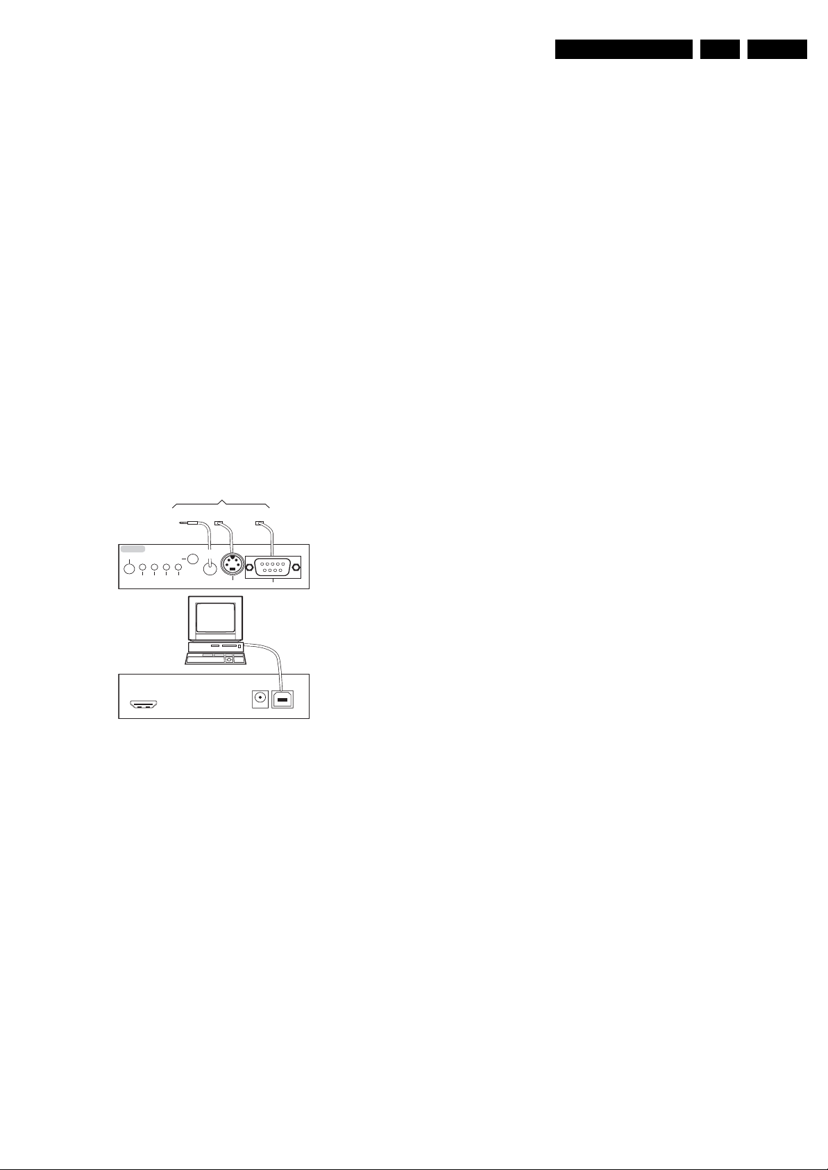
Service Modes, Error Codes, and Fault Finding
EN 39Q528.1A LA 5.
5.4 Service Tools
5.4.1 ComPair
Introduction
ComPair (Computer Aided Repair) is a Service tool for Philips
Consumer Electronics products. and offers the following:
1. ComPair helps you to quickly get an understanding on how
to repair the chassis in a short and effective way.
2. ComPair allows very detailed diagnostics and is therefore
capable of accurately indicating problem areas. You do not
have to know anything about I
yourself, because ComPair takes care of this.
3. ComPair speeds up the repair time since it can
automatically communicate with the chassis (when the uP
is working) and all repair information is directly available.
4. ComPair features TV software up possibilities.
Specifications
ComPair consists of a Windows based fault finding program
and an interface box between PC and the (defective) product.
The (new) ComPair II interface box is connected to the PC via
an USB cable. For the TV chassis, the ComPair interface box
and the TV communicate via a bi-directional cable via the
service connector(s).
How to Connect
This is described in the ComPair chassis fault finding database.
TO TV
TO
TO
I2C SERVICE
CONNECTOR
Multi
function
2
C
I
PC
ComPair II Developed by Philips Brugge
Optional power
UART SERVICE
CONNECTOR
5V DC
ComPair II
RC in
Optional
Switch
Power ModeLink/
Activity
HDMI
I
2
C only
RC out
UART SERVICE
CONNECTOR
Figure 5-13 ComPair II interface connection
Caution: It is compulsory to connect the TV to the PC as
shown in the picture above (with the ComPair interface in
between), as the ComPair interface acts as a level shifter. If
one connects the TV directly to the PC (via UART), ICs will be
blown!
How to Order
ComPair II order codes:
• ComPair II interface: 3122 785 91020.
• ComPair32 CD (update): 3122 785 60160.
•ComPair I
with chassis L01, A02, A10, EMX, ...).
•ComPair I
2
C interface cable: 3122 785 90004 (to be used
2
C interface extension cable: 3139 131 03791 (to
be used with chassis L01, A02, A10, L04, LC4, LC7.1,
LC7.2).
• ComPair UART interface cable: 3122 785 90630 (to be
used with chassis LC4, EJ3, BJ2, BL2, BP2, ...).
• ComPair RS232 cable: 3104 311 12742 (to be used with
chassis Q52x).
•ComPair I
with chassis TPM1.xA).
•ComPair I
2
C adapter cable: 3122 785 90004 (to be used
2
C interface cable: 9965 100 07325 (to be used
with chassis LC7.5).
2
C or UART commands
TO
RS232 /UART
G_06532_036.eps
240807
• ComPair UART interface cable: 3138 188 75051 (to be
used with chassis LC7.5).
Note: If you encounter any problems, contact your local
support desk.
5.4.2 LVDS Tool
Support of the LVDS Tool has been discontinued.
5.5 Error Codes
5.5.1 Introduction
The error code buffer contains all detected errors since the last
time the buffer was erased. The buffer is written from left to
right, new errors are logged at the left side, and all other errors
shift one position to the right.
When an error occurs, it is added to the list of errors, provided
the list is not full. When an error occurs and the error buffer is
full, then the new error is not added, and the error buffer stays
intact (history is maintained).
To prevent that an occasional error stays in the list forever, the
error is removed from the list after more than 50 hrs. of
operation.
When multiple errors occur (errors occurred within a short time
span), there is a high probability that there is some relation
between them.
Basically there are three kinds of errors:
• Errors detected by the Stand-by software. These errors
will always lead to protection and an automatic start of the
blinking LED for the concerned error (see paragraph “The
Blinking LED Procedure”). In these cases SDM can be
used to start up (see chapter “Stepwise Start-up”). Note
that it can take up to 90 seconds before the TV goes to
protection and starts blinking the error (e.g. error 53)
• Errors detected by main software that lead to
protection. In this case the TV will go to protection and the
front LED should also blink the concerned error. See also
paragraph “Error Codes” -> “Error Buffer” -> “Extra Info”.
For this chassis only error 63 is a protection error detected
by main software.
• Errors detected by main software that do not lead to
protection. In this case the error will be logged into the
error buffer and can be read out via ComPair, via blinking
LED method, or in case you have picture, via SAM.
5.5.2 How to Read the Error Buffer
Use one of the following methods:
• On screen via the SAM (only if you have a picture). E.g.:
– 00 00 00 00 00: No errors detected
– 06 00 00 00 00: Error code 6 is the last and only
detected error
– 09 06 00 00 00: Error code 6 was first detected and
error code 9 is the last detected error
• Via the blinking LED procedure (when you have no
picture). See next paragraph.
•Via ComPair.
• Via CSM. when CSM is activated the blinking LED
procedure will start and the CSM content will be written to
a USB stick (if present).
5.5.3 How to Clear the Error Buffer
Use one of the following methods:
• By activation of the “RESET ERROR BUFFER” command
in the SAM menu.
• With a normal RC, key in sequence “MUTE” followed by
“062599” and “OK”.
• If the content of the error buffer has not changed for 50+
hours, it resets automatically.
EN 40 Q528.1A LA5.
Service Modes, Error Codes, and Fault Finding
5.5.4 Error Buffer
In case of non-intermittent faults, clear the error buffer before
you begin the repair (before clearing the buffer, write down the
content, as this history can give you significant information).
This to ensure that old error codes are no longer present.
If possible, check the entire contents of the error buffer. In
some situations, an error code is only the result of another error
code and not the actual cause (e.g., a fault in the protection
detection circuitry can also lead to a protection).
There are several mechanisms of error detection:
• Via error bits in the status registers of ICs.
• Via polling on I/O pins going to the stand-by processor.
• Via sensing of analogue values on the stand-by processor
or the PNX85xx.
• Via a “not acknowledge” of an I
2
C communication.
Take notice that some errors need more than 90 seconds
before they start blinking or before they will be logged. So in
case of problems wait 2 minutes from start-up onwards, and
then check if the front LED is blinking or if an error is logged.
Table 5-2 Error code overview
Error Description Error/
2
C3 E MIPS PNX85xx Error logged.
3I
5 PNX85xx does
not boot (HW
cause)
6 5V, 12V supply P Stby P / Protection + Error
8 1V2, 1V4, 2V5,
3V3 supply
9 Supply fault P Stby P / Protection + Error
2
11 I
C-MUX1 E MIPS PCA9540 Error logged.
2
C-MUX2 E MIPS PCA9540 Error logged.
12 I
22 PNX5050 E MIPS PNX5050 Error logged.
23 HDMI multiplexer E MIPS AD8190/
2
24 I
C switch E MIPS PCA9540 Error logged.
26 Master IF E MIPS TDA9898/
28 MOP (Ambilight
MOP on DFI
1)
panel)
34 Tuner E MIPS TD1716 Error logged.
37 Channel decoder E MIPS TDA10060/
46 Pacific3 E MIPS T6TF4 Error blinking + Error
53 PNX85xx does
not boot (SW
cause)
63 Power OK E/P MIPS / Error logged in case of
65 DFI (EPLD on
DFI panel)
1)
Detected
Prot
by
E Stby P PNX85xx Error blinking.
P Stby P / Protection + Error
E MIPS EP2CXXF4
E Stby P PNX85xx Error blinking.
E MIPS / Error blinking + Error
Device Result
AD8191
9897/9890
84C7N
TDA10048
Note
1). Where applicable.
Extra Info
• Rebooting. When a TV is constantly rebooting due to
internal problems, most of the time no errors will be logged
or blinked. This rebooting can be recognized via a ComPair
interface and Hyperterminal (for Hyperterminal settings,
see paragraph “Stand-by software upgrade). You will see
that the loggings which are generated by the main software
keep continuing. In this case (rebooting) diagnose has to
be done via ComPair.
• Error 3 (I
2
C bus 3 blocked). At the time of release of this
manual, this error was not working as expected (error 3 is
logged and can be read out). Current situation: when this
error occurs, the TV will constantly reboot due to the
blinking.
blinking.
blinking.
Error logged.
Error logged.
Error logged.
Error logged.
logged.
a PDP set. Protection
in case of an LCD set.
logged.
blocked bus. The best way for further diagnosis here, is to
use ComPair (e.g. read out the NVM content). Instead of
error “3” it is possible you will see error “2” in the error
buffer.
• Error 5 (PNX85xx doesn’t boot). Indicates that the main
processor was not able to read his bootscript. This error will
point to a hardware problem around the PNX85xx (supplies
not OK, PNX 8535 completely dead, I
and Stand-by Processor broken, etc...). When error 5
occurs it is also possible that I
2
I
C2 can be indicated in the schematics as follows: SCL-
2
C link between PNX
2
C2 bus is blocked (NVM).
UP-MIPS, SDA-UP-MIPS, SCL-SLAVE, SDA-SLAVE,
SCL-2 or SDA-2.
• Error 11 (I
2
I
C-MUX1 bus. At the time of release of this manual, this
2
C MUX1). Indicates a blocked (short circuited)
error was not working as expected. Current situation: when
this error occurs the TV will constantly reboot due to the
blocked bus. The best way for further diagnosis, is to use
ComPair (e.g. read out the NVM content).
• Error 12 (I
2
I
C-MUX2 bus. At the time of release of this manual, this
2
C MUX2). Indicates a blocked (short circuited)
error was not working as expected. Current situation: when
this error occurs the TV will constantly reboot due to the
blocked bus. The best way for further diagnosis, is to use
ComPair (e.g. read out the NVM content).
• Error 24 (I
2
C switch). As a side effect of error 24 it is
possible that error 47(no existing error) will also be logged.
• Error 28 (DFI Ambilight MOP). It can take up to 2 minutes
or more before this error is logged. So if you suspect that
this MOP is defective: clear the error buffer, restart the TV
and wait for about 2 minutes before checking the error
buffer.
• Error 37 (Channel decoder). When this error occurs,
there probably will be no picture and sound from tuner
input. As a side effect of error 37 it is possible that error 4
(no existing error) is also logged.
• Error 46 (Pacific 3). When there is an actual problem with
or around the Pacific during start-up, you will have no
picture and error 46 will be blinked via the blinking LED
procedure. For further diagnosis you can always dump the
CSM content on USB stick (see CSM) or use ComPair.
• Error 53. This error will indicate that the PNX85xx has read
his bootscript (if this would have failed, error 5 would blink)
but initialization was never completed because of hardware
problems (NAND flash, ...) or software initialization
problems. Possible cause could be that there is no valid
software loaded (try to upgrade to the latest main software
version). Note that it can take up to 2 minutes before the TV
starts blinking error 53.
• Error 63 (POWER OK). When this error occurs, it means
that the POWER-OK line did not became “high”. This error
is only applicable for TV’s with an LCD display. For PDP
displays there will be no protection during a POWER-OK
line failure, but error 63 will be logged in the error buffer.
Caution: in case a PDP TV ends up into power-ok
protection, it can indicate that the display option code is set
to “LCD”. To change the display option code to “PDP” you
need to activate SDM via the service pads (see figure
“Service mode pads”). Then change the display option
code blindly via a standard RC: key in the code “062598”
directly followed by the “MENU” button and “XXX” (where
XXX is the 3 digit decimal display option code as
mentioned in figure “Display option code overview”).
• Error 65 (DFI EPLD error). When this error occurs it
means that there is a problem with the I
2
C communication
towards the EPLD (picture processing EPLD, not the
Ambilight EPLD) on the DFI panel.

Service Modes, Error Codes, and Fault Finding
EN 41Q528.1A LA 5.
5.6 The Blinking LED Procedure
5.6.1 Introduction
The blinking LED procedure can be split up into two situations:
• Blinking LED procedure in case of a protection. In this case
the error is automatically blinked. This will be only one
error, namely the one that is causing the protection.
Therefore, you do not have to do anything special, just read
out the blinks. A long blink indicates the decimal digit, a
short blink indicates the units.
• Blinking LED procedure in the “on” state. Via this
procedure, you can make the contents of the error buffer
visible via the front LED. This is especially useful for fault
finding, when there is no picture.
When the blinking LED procedure is activated in the “on” state,
the front LED will show (blink) the contents of the error-buffer.
Error-codes > 10 are shown as follows:
1. “n” long blinks (where “n” = 1 - 9) indicating decimal digit,
2. A pause of 1.5 s,
3. “n” short blinks (where “n”= 1 - 9),
4. A pause of approx. 3 s,
5. When all the error-codes are displayed, the sequence
finishes with a LED blink of 3 s,
6. The sequence starts again.
Example: Error 12 8 6 0 0.
After activation of the SDM, the front LED will show:
1. 1 long blink of 750 ms (which is an indication of the decimal
digit) followed by a pause of 1.5 s,
2. 2 short blinks of 250 ms followed by a pause of 3 s,
3. 8 short blinks followed by a pause of 3 s,
4. 6 short blinks followed by a pause of 3 s,
5. 1 long blink of 3 s to finish the sequence,
6. The sequence starts again.
5.6.2 How to Activate
Use one of the following methods:
• Activate the SDM or CSM. The blinking front LED will
show the entire contents of the error buffer (this works in
“normal operation” mode).
• Transmit the commands “MUTE” - “062500” - “OK”
with a normal RC. The complete error buffer is shown.
Take notice that it takes some seconds before the blinking
LED starts.
• Transmit the commands “MUTE” - “06250x” - “OK”
with a normal RC (where “x” is a number between 1 and
5). When x= 1 the last detected error is shown, x= 2 the
second last error, etc.... Take notice that it takes some
seconds before the blinking LED starts.
5.7 Protections
5.7.1 Software Protections
Most of the protections and errors use either the stand-by
microprocessor or the MIPS controller as detection device.
Since in these cases, checking of observers, polling of ADCs,
and filtering of input values are all heavily software based,
these protections are referred to as software protections.
There are several types of software related protections, solving
a variety of fault conditions:
• Protections related to supplies: check of the 12V, +5V,
+1V2, +1V4, 2V5 and +3V3.
• Protections related to breakdown of the safety check
mechanism. E.g. since the protection detections are done
by means of software, failing of the software will have to
initiate a protection mode since safety cannot be
guaranteed any more.
Remark on the Supply Errors
The detection of a supply dip or supply loss during the normal
playing of the set does not lead to a protection, but to a cold
reboot of the set. If the supply is still missing after the reboot,
the TV will go to protection.
Protections during Start-up
During TV start-up, some voltages and IC observers are
actively monitored to be able to optimise the start-up speed,
and to assure good operation of all components. If these
monitors do not respond in a defined way, this indicates a
malfunction of the system and leads to a protection. As the
observers are only used during start-up, they are described in
the start-up flow in detail (see paragraph “Stepwise Start-up”).
5.7.2 Hardware Protections
The only real hardware protection in this chassis is (in case of
an audio problem) the audio protection circuit that will switch
“off” immediately the supply of the SSB. The supply will buzz
during the protection and +12VS drops to approx. 5V5 and +5V
Stand-by to approx. to 1V9. Other indication of the audio
protection is that the red LED lights up with an intensity of 50%.
Repair Tips
• It is also possible that you have an audio DC protection
because of an interruption in one or both speakers (the DC
voltage that is still on the circuit cannot disappear through
the speakers). Caution: (dis)connecting the speaker wires
during the ON state of the TV at high volume can damage
the audio amplifier.
5.8 Fault Finding and Repair Tips
Read also paragraph “Error Codes” -> “Error Buffer” -> “Extra
Info”.
5.8.1 Ambilight
Due to a degeneration process of the AmbiLight, it is
recommended to change both ambilight units in case one unit
needs to be repaired.
5.8.2 Audio Amplifier
It is recommended to replace all components at once (7D06,
7D09, 3D01, 3D25) when a defective FET 7D10 needs to be
fixed. For the left channel (defective FET 7D35) of the audio
amplifier replace all components like 7D31, 7D34, 3D11, 3D28.

EN 42 Q528.1A LA5.
Service Modes, Error Codes, and Fault Finding
5.8.3 CSM
When you activate CSM and there is a USB stick connected to
the TV, the software will dump the complete CSM content to the
USB stick. The file (Csm.txt) will be saved in the root of your
USB stick. If this mechanism works you can conclude that a
large part of the operating system is already working (MIPS,
USB...)
5.8.4 DC/DC Converter
Introduction
• The best way to find a failure in the DC-DC converters is to
check their starting-up sequence at “power-on via the
mains cord”, presuming that the standby microprocessor is
operational.
• If the input voltage of DC-DC converters is around 12.7V
(measured on decoupling capacitors 2U03/2U93/2U6S
and 2U6R) and the enable signals are “low” (active) then
the output voltages should have their normal values. +12V
and +5V-POD supplies start-up first (enabled by PODMODE signal from the standby microprocessor). There is a
supplementary condition for +12V to start-up: if +5V-POD
does not start up due to a local defect, then +12V will not
be available as well. +5V-ON supply is enabled by the ONMODE signal (coming also from the standby
microprocessor) and is coming up a little bit later (20 ms)
due to the slower rise time needed to charge the USB
decoupling capacitor 2N31. +1V2 supply starts-up when
+12V appears, then at least 100 ms later, +1V8, +2V5 and
+3V3 will be activated via the ENABLE-3V3 signal from the
standby microprocessor. If +12V value is less than 10 V
then the last enumerated voltages will not show-up due to
the under-voltage detection circuit 6U10 + 7U10 and
surrounding components. Furthermore, if +12V is less than
8V then also +1V2 will not be available. The third DC-DC
convertor that delivers +1V4 out of +12V is started up when
the ENABLE-1V2 becomes active (low) and +12V is
present. The +Vtun generator (present only for the
analogue version of China platforms) will generate +33V
for the analogue tuner as soon as the 12V/3.3V DC-DC
converter will start to operate.
• The consumption of controller IC 7U00 is around 19 mA
(that means almost 200 mV drop voltage across resistor
3U01) and the consumption of controller IC 7U64 is around
12 mA.
• The current capability of DC-DC converters is quite high
(short-circuit current is 7 to 10 A), therefore if there is a
linear integrated stabiliser that, for example, delivers 1.8V
from +3V3 with its output overloaded, the +3V3 stays
usually at its normal value even though the consumption
from +3V3 increases significantly.
• The +1V8 and +2V5 supply voltages are obtained via linear
stabilizer made with discrete components that can deliver
a lot of current, therefore in case +1V8 or +2V5 are shortcircuited to GND then +3V3 will not have the normal value
but much less.
• The SUPPLY-FAULT signal (active low) is an internal
protection (error 9) of the DC-DC convertor and will occur
if the output voltage of any DC-DC convertor is out of limits
(10% of the normal value).
Fault Finding
• Symptom: +1V2 not present (even for a short while
~10 ms)
1. Check 12 V availability (resistor 3U01, MOS-FETs
7U03 and 7U08), value of +12 V, +12 V switch (7U14
+ 7U16 and surrounding components) and +5V-POD.
2. Check the voltage on pin 9 (1.5 V),
3. Check for +1V2 output voltage short-circuit to GND that
can generate pulsed over-currents 7...10 A through coil
5U02.
4. Check the over-current detection circuit (2U20 or 3U40
interrupted).
• Symptom: +1V4 not present (even for a short while
~10ms) while +12V is okay (also across input capacitors
2U6S and 2U6R).
1. Check resistor 3U7B and power MOS-FETs 7U61-1/2
2. Check the voltage on pin 4 (4 V)
3. Check enable signal ENABLE-1V2 (active “low”)
4. Check for +1V4 output voltage short-circuit to GND that
can generate pulsed over-currents 7...10 A through coil
5U60
5. Check the over-current detection reference(2U65 +
3U7C) and the boot components (2U66 + 6U60).
•
Symptom: +1V2 present for about 100ms, +1V8, +2V5
and +3V3 not rising.
1. Check the ENABLE-3V3 signal (active “low”),
2. Check the voltage on pin 8 (1.5 V),
3. Check the under-voltage detection circuit (the voltage
on collector of transistor 7U10-1 should be less than
0.8 V),
4. Check for output voltages short-circuits to GND (+3V3,
+2V5 and +1V8) that can generate pulsed overcurrents 7...10 A through coil 5U01,
5. Check the over-current detection circuit (2U18 or 3U31
interrupted).
• Symptom: +1V2 OK, +2V5 and +3V3 present for about
100 ms. Possible cause: SUPPLY-FAULT line stays “low”
even though the +3V3 and +1V2 is available - the standby
microprocessor is detecting that and switching “off” all
supply voltages.
1. Check the drop voltage across resistor 3U01 or 3U7B
(they could be too high, meaning a defective controller
IC or MOS-FETs),
2. Check if the boost voltage on pin 4 of controller IC
7U00 is less than 14 V (should be 19 V),
3. Check if +1V2 or +3V3 are higher than their normal
values - that can be due to defective DC feedback of
the respective DC-DC convertor (ex. 3U47, 3U77,
3U7L, 3U7J or 3U70).
• Symptom: +1V2, +1V4, +1V8, +2V5 or +3V3 shows a high
level of ripple voltage (audible noise can come from the
filtering coils 5U01, 5U02 or 5U60). Possible cause:
instability of the frequency and/or duty cycle of a DC-DC
converter or stabilizer.
1. Check the resistor 3U32 and 3U7D, capacitors 2U17
and 2U19, input and output decoupling capacitors.
2. Check a.c. feedback circuits
(2U23+2U24+3U55+3U63 for +1V2,
2U6D+2U6E+2U6G+3U6A+3U7E for +1V4 and
2U07+2U08+3U17+3U24 for +3V3), compensation
capacitors 2U25, 2U34, 2U36, 2U37, 2U40, 2U43,
2U68 and 2U6B.
• Symptom: +1V2, +1V4, +2V5 and +3V3 ok, no +Vtun
(analogue sets only). Possible cause: the “+VTUN
GENERATOR” circuit (7U24+7U26+surroundings
components) is defective: check transistor 7U24 (it has to
have gate voltage pulses of about 10 V amplitude and drain
voltage pulses of about 35 V amplitude) and surroundings
components. A high consumption (more than 6 mA) from
+Vtun voltage can cause also +Vtun voltage to be too low
or zero.
Note: when a pair of power MOSFETs(7U01+7U06,
7U03+7U08 or 7U61-1/2) becomes defective the controller IC
7U00 or 7U64 should be replaced as well.

Service Modes, Error Codes, and Fault Finding
5.8.5 Exit “Factory Mode”
When an “F” is displayed in the screen's right corner, this
means that the set is in “Factory” mode, and it normally
happens after a new SSB has been mounted.
To exit this mode, push the “VOLUME minus” button on the
TV’s keyboard control for 5 seconds and restart the set.
5.8.6 Sanken display supply
The 47" sets in this chassis come with a Sanken buy-in supply.
The result of a failing Sanken display supply, e.g. one of the
following voltages is missing: +400V, +12V or +24V, will lead to
protection (blinking error 63). The set is switched off.
When the primary circuit of the on-board platform supply fails,
there is a high possibility that the main fuse of the Sanken
display supply will break. In this case the Sanken display
supply must not be replaced completely, just replace the
Sanken main value fuse and repair the on-board platform
supply. For safety reasons, make sure to use the correct fuse
type.
5.8.7 SSB service supply connector
Connector 1B40 can be used to apply external supply (+12V
and +5V). In this way you do not need mains supply for
troubleshooting on the SSB. e.g. component level repair.
EN 43Q528.1A LA 5.
5.8.8 Tuner
For access to the components located under the tuner itself,
you need to desolder the ground connections and bend the
tuner up. To maintain a good performing tuner you must make
a new ground connection to the SSB, for instance by use of a
wire.
Caution: In case you replace the tuner, always check the tuner
option!
5.8.9 UI over PCI bus
The UI is not integrated in the RGB signal but is sent from
PNX85xx to PNX5050 via the PCI bus. TXT and MHEG are
integrated in the RGB signal. So if you have TXT signal but no
UI, check the PCI bus.

EN 44 Q528.1A LA5.
5.8.10 SSB Replacement
Follow the instructions in the flowchart in case you have to
exchange the SSB. See figure “SSB replacement flowchart”.
Service Modes, Error Codes, and Fault Finding
START
Set is still
operating?
Set is starting up but no display
Upgrade main TV SW to the latest version via
USB stick (#)
Program “Display Option” code via 062598
MENU, followed by 3 digits code (this code
can be found on a sticker inside the set or in
the Service Manual)
After entering “Display Option” code, set is
going to Standby (= validation of code)
Restart the set
Yes
No
Activate SAM and save the TV settings
via “Upload to USB”
- Replace SSB board by a Service SSB.
- Make the SSB fit mechanically to the set.
Start-up set
If necessary, adapt the connector plate and/or
the shielding to make the assy fit
mechanically.
Set behaviour?
Set is starting up & display is OK
Set goes into protection
Activate SDM via shorting the Service pins on
the SSB
- Program Display Option code via 062598 MENU followed by the 3 digit code
(see sticker inside set or in the Service Manual)
- Or program “Display Option” code in SAM via “062596 i+”, Options, Display, Screen
Method 1; In some sets it is possible to
program “Display Option” code before set is
going into protection.
If set is starting-up in Factory mode “F”, push
the “Volume minus” button on the local
keyboard for 5 seconds and restart the set
Method 2; First bring set in SDM and
program “Display Option” code.
Method 3; Bring the PDP power supply in
stand-alone mode and program the “Display
Option” code.
No
Connect ComPair, load JETT software and
program set type- and serial number
Update main and Standby software via USB
(#) Some new “Display Option” codes are not recognised
by SSB’s with old(er) SW, resulting in “no display”.
Therefore it is advised to ALWAYS update the main TV
SW (autorun.upg) via a USB stick to the latest version,
before setting the “Display Option” code
.
Figure 5-14 SSB replacement flowchart
Saved settings
on USB stick?
Yes
Activate SAM and reload settings
via “Download from USB”
Check latest software on Service website.
Check and perform alignments in SAM
according to the Service Manual
Check changes in CSM
END
In case of settings reloaded from USB, the set type- and
set serial number are automatically stored when entering
display options.
- Check if correct “Display Option” code is programmed.
- Verify “Option Codes” according sticker inside the set.
- Default settings for White drive ...see Service Manual
Instruction note SSB replacement
3122 785 00982
05-FEB-2007
H_16771_007.eps
130707

Service Modes, Error Codes, and Fault Finding
5.8.11 Display option code
Caution: In case you have replaced the SSB, always check the
display option code in SAM, even if you have picture. With a
wrong display option code it is possible that you have picture,
but that in certain conditions you have unwanted side-effects.
5.8.12 Upgrade EDID NVM
To upgrade the EDID NVM you must short circuit pin 7 of the
EDID NVM to ground. Therefore some test points (EDID1,
EDID2 and EDID3) are foreseen (figure “EDID-NVM pins”).
See ComPair for further instructions.
EN 45Q528.1A LA 5.
Figure 5-15 EDID-NVM pins
5.9 Software Upgrading
5.9.1 Introduction
The set software and security keys are stored in a NANDFlash, which is connected to the PNX85xx via the PCI bus.
It is possible for the user to upgrade the main software via the
USB port. This allows replacement of a software image in a
stand alone set, without the need of an E-JTAG debugger. A
description on how to upgrade the main software can be found
in the DFU.
Important: When the NAND-Flash must be replaced, a new
SSB must be ordered, due to the presence of the security
keys!!! (copy protection keys, MAC address, ...).
Perform the following actions after SSB replacement:
1. Set the correct option codes (see sticker inside the TV).
2. Update the TV software (see the DFU for instructions).
3. Perform the alignments as described in chapter 8 (section
“Reset of Repaired SSB”).
4. Check in CSM if the HDMI keys are valid.
H_16800_122.eps
240707
5.9.2 Main Software Upgrade
The software image resides in the NAND-Flash, and is
formatted in the following way (refer to figure “NAND-flash
content”):

EN 46 Q528.1A LA5.
Service Modes, Error Codes, and Fault Finding
Nand Flash content
JFFS2 partition 1
(application read write data)
JFFS2 partition 0
(Application read only once data)
JFFS2 partition 0
(Application read only upgradable data)
SQUASHFS partition
BFFS partition 2 (DVD OK)
BFFS partition 1 (DVD cursor down)
BFFS partition 0
Block 0
hC
d pu kcab ,syek IMDH
wizard pictures, display file, cabinet file,
upgrade assistant, …
Main software (Mips)
Linux structure (root file system)
Default software upgrade application
TriMedia software
boot batch file 2
Back up software upgrade application
boot batch file 1
Linux kernel
JETT : needed for ComPair
Jaguar Boot loader
boot batch file 0
µBTM
partition table
Figure 5-16 NAND-Flash content
• The above overview of the NAND Flash shows the content
of the different partitions. It also shows which part of the
one-zip file erases and programs which part of the NAND
Flash.
• Remark: the above does not mean that you can reprogram
your HDMI keys with the “UpgradeAll.upg” file from the one
zip file. This can only be done in a secure environment (e.g.
the factory).
• The “UpgradeAll.upg” file is only used in the factory.
• The “FlashUtils.upg” file is only used by service centra
which are allowed to do component level repair on the
SSB.
Automatic Software Upgrade
In “normal” conditions, so when there is no major problem with
the TV, the main software and the default software upgrade
application can be upgraded with the “AUTORUN.UPG” (FUS
part of the one-zip file: e.g. 3104 337 03801 _FUS _Q581E_
0.37.0.0_commercial.zip). This can also be done by the
consumers themselves, but they will have to get their software
from the commercial Philips website or via the Software Update
Assistant in the user menu (see DFU). The “autorun.upg” file
must be placed in the root of your USB stick.
How to upgrade:
1. Copy “AUTORUN.UPG” to the root of your USB stick.
2. Insert USB stick in the side I/O while the set is in ON
MODE. The set will restart and the upgrading will start
automatically. As soon as the programming is finished, you
will get the message that you can remove your USB stick
and restart the set.
ONE ZIP
FUS UPG UpgradeAll UPG
XXX
XXXX
XXXX
XXXX
XXX… ,atad GPE ,elbat lenna
XX… ,elif yalpsi
FlashUtils UPG
margorpesaremargorpesaremargorpesaretnetnoCnoititraP
XX
X
H_16770_099.eps
220307
Attention!
In case that you have started the download application
manually, the “autorun.upg” will maybe not be recognized.
What to do in this case:
1. Create a directory “UPGRADES” on your USB stick.
2. Rename the “autorun.upg” to something else, e.g. to
“software.upg”. Do not use long or complicated names,
keep it simple. Make sure that “AUTORUN.UPG” is no
longer present in the root of your USB stick.
3. Copy the renamed “upg” file into this directory.
4. Insert USB stick in the side I/O.
5. The renamed “upg” file will be visible and selectable in the
upgrade application.
Back-up Software Upgrade Application
If the default software upgrade application does not start (could
be due to a corrupted boot 2 sector) via the above described
method, you can try to activate the “back-up software upgrade
application”.
How to start the “back-up software upgrade application”
manually:
1. Disconnect the TV from the Mains/AC Power.
2. Press the “CURSOR DOWN” button on a Philips DVD RC6 remote control (it is also possible to use the TV remote in
“DVD” mode). Keep the “cursor down” button pressed
while reconnecting the TV to the Mains/AC Power.
3. The software upgrade application will start.
Manual Software Upgrade
In case that the software upgrade application does not start
automatically, you can also start it manually.
How to start the software upgrade application manually:
1. Disconnect the TV from the Mains/AC Power.
2. Press the “OK” button on a Philips DVD RC-6 remote
control (it is also possible to use the TV remote in “DVD”
mode). Keep the “OK” button pressed while reconnecting
the TV to the Mains/AC Power.
3. The software upgrade application will start.

Service Modes, Error Codes, and Fault Finding
EN 47Q528.1A LA 5.
5.9.3 Stand-by Software Upgrade
There are two methods now to upgrade stand-by software:
Upgrade via USB
In this chassis it is possible to upgrade the Stand-by software
via a USB stick. The method is similar to upgrading the main
software via USB.
Use the following steps:
1. Create a directory “UPGRADES” on your USB stick.
2. Copy the Stand-by software (part of the one-zip file, e.g.
StandbySW_CFT01_9.0.0.0.upg) into this directory.
3. Insert the USB stick into the TV.
4. Start the download application manually (see paragraph
“Manual start of the Software Upgrade Application”.
5. Select the appropriate file and press the “red” button to
upgrade.
Upgrade via PC and ComPair interface
It will be possible to upgrade the Stand-by software via a PC
and the ComPair interface. Check paragraph “ComPair” on
how to connect the interface. To upgrade the Stand-by
software, use the following steps:
1. Disconnect the TV from the Mains/AC Power.
2. Short circuit the SPI pins [2] on the SSB (see figure
“Service mode pads” earlier in this chapter).
3. Keep the SPI pins shortened while connecting the TV to
the Mains/AC Power.
4. Release the short circuit after approx. two seconds.
5. Start up HyperTerminal (can be found in every Windows
application via Programs -> Accessories ->
Communications -> HyperTerminal). Use the following
settings:
–COM1
– Bits per second = 38400 (9600)*
– Data bits = 8
– Parity = none
– Stop bits = 1
– Flow control = None
6. Press “Shift U” on your PC keyboard. You should now see
the following info:
– PNX2015 Loader V1.0
– 19-09-2003
– DEVID=0x05
–Erasing
– MCSUM=0x0000
–=
7. If you do not see the above info, restart the above
procedure, and check your HyperTerminal settings and the
connections between PC and TV.
8. Via “Transfer” -> “Send text file ...”, you can send the
proper upgrade file to the TV (e.g. *.hex).
9. After successful programming, you must see the following
info (this can take several minutes!):
– DCSUM=0xC67E
–:Ok
– MCSUM=0xC67E
– Programming
– PCSUM=0xC67E
– Finished
10. If you do not see this info, restart the complete procedure.
11. Close HyperTerminal.
12. Disconnect and connect Mains/AC Power again.
(*) When having problems with upgrading, use the values
between brackets.
5.9.4 Content and Usage of the One-Zip Software File
Below you find a content explanation of the One-Zip file, and
instructions on how and when to use it.
• 1.1 Ambilight_PRFAM_x.x.x.x.zip. Not to be used by
Service technicians.
• 1.2 Cabinet_ACOUS_x.x.x.x.zip. Not to be used by
Service technicians.
• 1.3 Ceisp2padll_P2PAD_x.x.x.x.zip. Not to be used by
Service technicians. For ComPair development only.
• 1.4 Display_DISPT_x.x.x.x.zip. Not to be used by Service
technicians.
• 1.5 EDID_Q581X_x.x.x.x.zip. Contains the EDID content
of the different EDID NVM’s. See ComPair for further
instructions.
For sets with three HDMI connectors.
- For HDMI 1 NVM, use “*port 1*.bin
- For HDMI 2 NVM, use “*port 2*.bin
- For HDMI 3 NVM, use “*port 3*.bin
• 1.6 EJTAGDownload_Q581X_x.x.x.x.zip. Only used by
service centra which are allowed to do component level
repair.
• 1.7 Factory_Q581X_x.x.x.x_commercial.zip. Only for
production purposes, not to be used by Service
technicians.
• 1.8 FlashUtils_Q581X_x.x.x.x_commercial.zip. Not to
be used by Service technicians.
• 1.9 FUS_Q581X_x.x.x.x_commercial.zip. Contains the
“autorun.upg” which is needed to upgrade the TV main
software and the software download application.
• 2.0 MOP_IACXX_x.x.x.x.zip. Not to be used by Service
technicians. A programmed MOP device can be ordered
via your regional Service organization.
• 2.1 OpenSourceFile_Q581X_x.x.x.x.zip. Not to be used
by Service technicians.
• 2.2 Pacific3_P3FW0_x.x.x.x.zip. Not to be used by
Service technicians. A programmed PACIFIC device can
be ordered via your regional Service organization.
• 2.3 PQPrivate_U5207_x.x.x.x.zip. Not to be used by
Service technicians.
• 2.4 PQPublic_U5207_x.x.x.x.zip. Not to be used by
Service technicians.
• 2.5 ProcessNVM_Q531X_x.x.x.x.zip. Default NVM
content. Must be programmed via ComPair.
• 2.6 StandbySW_CFTxx_x.x.x.x_commercial.zip.
Contains the Stand-by software in “upg” and “hex” format.
- The “StandbySW_xxxxx_prod.upg” file can be used to
upgrade the Stand-by software via USB.
- The “StandbySW_xxxxx.hex” file can be used to upgrade
the Stand-by software via ComPair.
-The files “StandbySW_xxxxx_exhex.hex” and
“StandbySW_xxxxx_dev.upg” may not be used by Service
technicians (only for development purposes).
• 2.7 UpgradeAll_Q531X_x.x.x.x_commercial.zip. Only
for production purposes, not to be used by Service
technicians.
Caution: Never use this file, because it will overwrite
the HDCP keys! ! !

EN 48 Q528.1A LA5.
Personal Notes:
Service Modes, Error Codes, and Fault Finding
E_06532_012.eps
131004
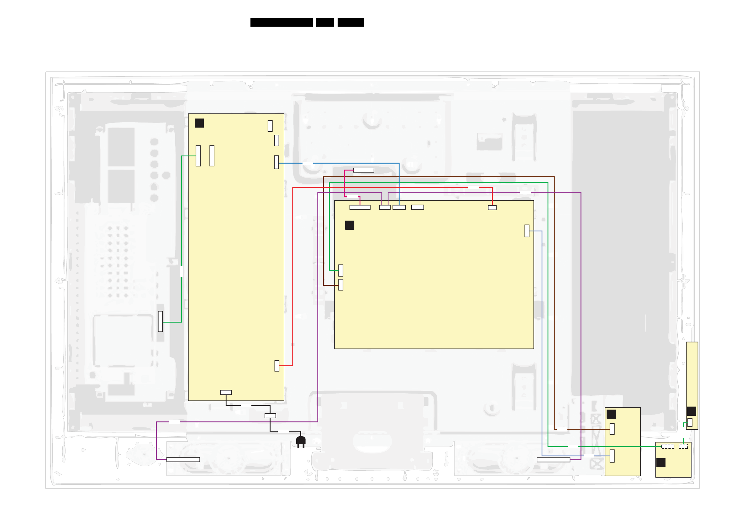
Block Diagrams, Test Point Overview, and Waveforms
6. Block Diagrams, Test Point Overview, and Waveforms
Wiring Diagram 32” LCD
WIRING 32” LCD
(STYLING ME7)
DISPLAY SUPPLY
A
(1050)
12P
14P
1317
1320
1M12
4P
1M09
1P11
4P
8P
8411
49Q528.1A LA 6.
CONNECTOR
LCD DISPLAY
(1004)
lLVDS
51P
INVERTER
8402
8150
41P
1G50
SSB
B
(1011)
7P
8319
14P
1320
2P3
1P02
1M20
4P
1H01
17354P1P11
5P
8P
1M59
2P3
1P02
8738
1M36
11P
8738
RIGHT SPEAKER
(5214)
(5216)
1308
2P3
8408
INLET
8194
LEFT SPEAKER
(5213)
(5215)
8201
8120
8136
D
4P
11P
SIDE I/O
(1015)
1309
1304
7P
1M20
IR/LED/LIGHT
J
SENSOR
(1012)
KEYBOARD CONTROL
3P
8101
3P
1M01
H_16790_063.eps
300807
(1010)
E
1M01

Block Diagrams, Test Point Overview, and Waveforms
Wiring Diagram 42” LCD
WIRING 42” LCD + DFI + AMBI LIGHT (STYLING ME7)
50Q528.1A LA 6.
AMBI-LIGHT UNIT (IN BACK COVER)
1M09
1M59
1M82
(1175)
4P
5P
7P
INVERTER
LCD DISPLAY
8682
8319
DISPLAY SUPPLY
A
14P
1319
2P3
1P02
14P
1319
12P
1317
4P
1M09
1M90
6P
8P
1P11
LVD S
51P
8411
LVD S
41P
8250
41P
1G50
SSB
B
7P
1M20
4P
1H01
17354P1P11
5P
8P
1M59
(1004)
8252
8738
8402
8251
8316
2P3
1P02
AB
41P
51P
41P
8590
DFI PANEL
1F50
1F51
1F52
11P
1M36
8509
1M90
1M09
1M12
1M59
6P
4P
8609
4P
7P
8659
5P
12P
1317
INVERTER
1M82
5P
1M59
4P
1M09
RIGHT SPEAKER
1308
2P3
INLET
(1176)
AMBI-LIGHT UNIT (IN BACK COVER)
8408
(1010)
KEYBOARD CONTROL
E
3P
1M01
8101
3P
1M01
H_16790_064.eps
260907
LEFT SPEAKER
8136
8201
8120
D
SIDE I/O
(1015)
4P
1309
11P
1304
7P
1M20
IR/LED/LIGHT
J
SENSOR
(1012)

Block Diagrams, Test Point Overview, and Waveforms
Wiring Diagram 47”
WIRING 47” LCD + DFI + AMBI LIGHT
51Q528.1A LA 6.
(STYLING ME7)
(IN BACK COVER)
(1175)
AMBI-LIGHT UNIT
4P
1M09
5P
1M59
7P
1M82
LCD DISPLAY
8682
8319
4P
1M90
6P
1M12
1M09
LVD S
4P
8P
1P11
51P
8411
LVD S
41P
8250
17354P1P11
8P
1M59
41P
1G50
SSB
B
12P
1317/1321
13P14
1316/1319
DISPLAY SUPPLY
(1050)
(1004)
8316
8402
8252
8251
8738
5P
2P3
1P02
AB
41P
51P
41P
8590
DFI PANEL
1F50
1F51
1F52
11P
1M36
8509
1M90
1M09
1M12
1M59
6P
4P
8609
4P
7P
8659
5P
1M82
5P
1M59
4P
1M09
(IN BACK COVER)
7P
1M20
4P
1H01
INVERTER INVERTER
1319
13P14
2P3
1P02
RIGHT SPEAKER
1308
2P3
INLET
8408
8201
LEFT SPEAKER
8136
8120
12P
1317
SIDE I/O
D
(1015)
4P
1309
11P
1304
7P
1M20
IR/LED/LIGHT
J
SENSOR
(1012)
(1176)
AMBI-LIGHT UNIT
(1010)
KEYBOARD CONTROL
E
3P
1M01
8101
3P
1M01
H_16790_065.eps
260907

Block Diagrams, Test Point Overview, and Waveforms
Wiring Diagram 42” (AUREA)
WIRING 42” LCD + DFI + AMBI LIGHT
52Q528.1A LA 6.
Styling AUREA
1M81
10P
10P
(1045)
DISPLAY SUPPLY
A
(1050)
AMBILIGHT MODULE
10P
(5215)
AMBILIGHT MODULE
14P
1319
12P
1317
(1045)
4P
1M09
1M80
10P
1M90
1M81
10P
8000
6P
8250
1P11
8P
8411
AMBILIGHT MODULE
LCD DISPLAY
8236
LVD S
51P
LVD S
41P
(1004)
8402
8252
8251
8235
(1046)
1M80
10P
8590
AB
41P
51P
41P
8000
DFI PANEL
(1130)
1F50
1F51
1F52
8681
1M81
10P
1M90
1M09
1M12
1M59
AMBILIGHT MODULE
8422
8680
6P
4P
4P
10P
2P
1P22
AUDIO AND AMBILIGHT
AP
SUPPLY
(1055)
10P
1M81
1M80
5P
8659
(1045)
1M80
10P
8580
10P
1M81
(1045)
AMBILIGHT MODULEAMBILIGHT MODULE
10P
1M80
(5216)
8000
10P
(1045)
5P
14P
1319
AMBILIGHT MODULE
8581
10P
(1010)
KEYBOARD CONTROL
E
3P
1M01
10P
1M80
2P3
1P22
2P3
1P02
AMBILIGHT MODULE
41P
4P
17354P1P11
8319
B
8316
7P
1M20
8191
8192 UK
4P
1H01
RIGHT SUBWOOFER
(5213)
(1045)
10P
1M81
1308
2P3
8120
8408
INLET
8000
1G50
SSB
(1011)
10P
1M80
1738
8101
5P
8P
1M59
3P
1M01
1M22
LED PANEL
7P
J
(1012)
AMBILIGHT MODULE
(1046)
2P3
1P02
10P
1M81
1317
8741
SIDE I/O
(1115)
1309
1304
8000
10P
1M81
(1045)
5P
8536
10P
1M80
5P
1M59
11P
1M36
4P
1741
12P
5P
1736
5P
1735
4P
1737
4P
1738
8535
D
8201
4P
LEFT SUBWOOFER
(5214)
8000
10P
1M80
AMBILIGHT MODULE
8136
(1045)
10P
1M81
11P
H_16801_115.eps
101007

Block Diagrams, Test Point Overview, and Waveforms
Block Diagram Supply 32”
DISPLAY SUPPLY + PLATFORM SUPPLY 32"
MAINS FILTER + STANDBY
A1
1308
5401
5403
5405
1400
2
T5AH
1
MAINS
FILTER
1450
7801
7802
ON/OFF
STANDBY
COLD GROUND
HOT GROUND
STANDBY
53Q528.1A LA 6.
SUPPLY
A2
14
7002
BIAS SUPPLY
6077
7007
7008
5009
HIGH
SIDE
DRIVE
LOW
SIDE
DRIVE
3033
2003
STP15NK50
STP15NK50
60786079
400V_HOT
7005
7006
VCC
3000
5017
5001
15
5015
14
OA
5016
12
OB
10
FI
6
7
4
2
10
9
3810
6807
TS6B
+
-
A2
5007
5008
25V_HOT
400V_HOT
7017
7018
SOFT
STAR T
CURRENT
PROTECTION
3021
7001
MC34067PG
11
OSCC
3007
CONTROL
7
ERROR
11
SOST
5
2014
VREF
7004
7009
OVER
VOLTAGE
PROTECTION
+
3100
5010
2017
5040
2011
TCET1102
2
3
5002
8
7
5
3
5028
9
10
5027
11
13
12
5025
14
15
5026
16
6044
6044
6044
3057
2020
3022
2022
3024
7010
TS2431
K
R
A
3030
3025
VS Voltage
Adj.
3026
MAINS FILTER + STANDBY
A1
+12Vd
+24V
+12Vd
6024
7013
3052
+5V2
Power-Good = 5V
if +12V >10V
30773078
A1
N.C
1M09
5406
+12Vd
+5V2
A1
STANDBY
BOOST
ON-OFF
POWER-GOOD
DIM-CONTROL
1320
1317
1P11
1
2
1
2
3
4
5
11
12
1
2
3
4
5
11
12
8
7
6
5
4
3
2
1
TO
AMBI-LIGHT
TO
DISPLAY
TO
DISPLAY
TO 1P11
A2
SSB
1P02
22
11
B01A
1P02
SUPPLY
1B32
T1.6A
5B00
6B04
SS36
HOT GROUND COLD GROUND
3B61
2B48
6B07
2B51
6B08
6B06
2B46
6B05
2B45
7B50
CONTROL
1B33
2.5AT
AUDIO-PROT
B11C
7B06
+AUDIO-POWER
-AUDIO-POWER
+12VS
3B72
3B73
6B15
K
A
3B29
R
+5V-STANDBY
1B40
1
FOR SERVICE
2
TO PROVIDE
3
EXTERNAL
SUPPLY
4
H_16800_099.eps
110507
+
7B00
-
7B01
3B60
7B02
7B05
CONTROL
3B50
3B51
HOT GROUND COLD GROUND
5B01
5
3
2
1
7
8
9
10
11
12
14
7B04
TCET1102
2
3
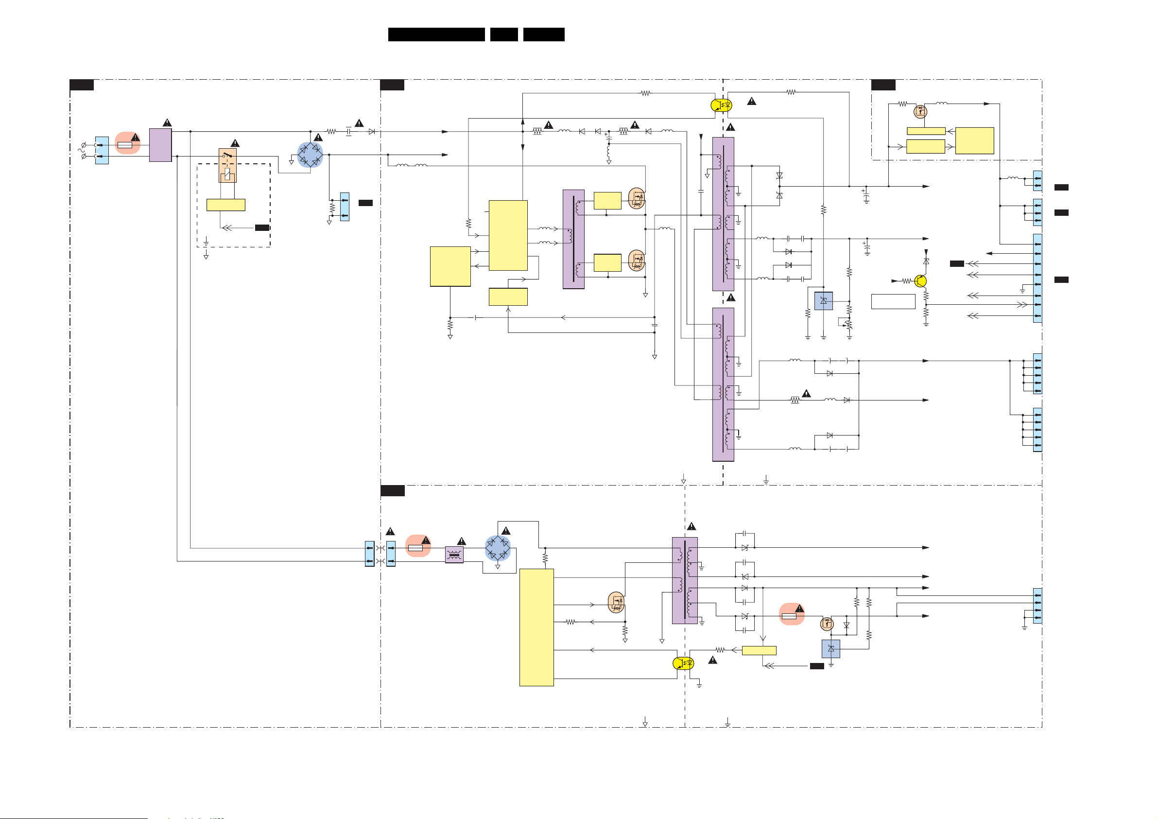
Block Diagrams, Test Point Overview, and Waveforms
Block Diagram Supply 37” - 42”
SUPPLY 37”- 42"
MAINS FILTER + STANDBY
A1
5305
1308
1314
2
T5AH
1
5306
MAINS
FILTER
7308
7309
COLD GROUND
HOT GROUND
1350
3
4
ON/OFF
STANDBY
2
1
Standby
54Q528.1A LA 6.
SUPPLY
A2
BIAS SUPPLY
2327
3318
6307
GBJ6J
+
-
3330
A2
1P22
1
2
6304
TO 1P22
AP1
AUDIO AMBI
SUPPLY
5007
5008
25V_HOT
400V_HOT
7011
7012
SOFT
STAR T
CURRENT
PROTECTION
3021
7001
MC34067PG
11
OSCC
3007
CONTROL
7
ERROR
11
SOST
5
2014
VREF
7004
7009
OVER
VOLTAGE
PROTECTION
+
VCC
3000
5017
5001
15
5015
14
OA
12
OB
10
FI
5016
4
2
6033
5009
7007
HIGH
6
SIDE
DRIVE
7
7008
LOW
10
SIDE
DRIVE
9
3075
2003
STP15NK50
STP15NK50
7005
7006
3065
14
7002
TCET1102
2
3
60246032
5010
400V_HOT
5012
2060
5011
2059
5002
5025
5026
6074
6075
3057
2029
6021
6041
2045
2034
2039
3022
3024
7010
TS2431
K
R
A
3030
3025
VS Voltage
Adj.
3026
A3
2020
2022
+5V2
Power-Good = 5V
if +12V >10V
DC-DC
3407
7402
GATE DRIVER
UNDERVOLTAGE
LOCKOUT
+18V OR +12V
+24VA OR +295V
7015
3052
+12V
6076
30963097
5401
7401
CONTROLLER
A1
A1
N.C
TO
DISPLAY
TO
DISPLAY
+12V
+5V2
Standby
Boost
Light_on_of
Power-Good
DIM-control
5028
1M09
1M90
1P11
1
2
1
2
3
8
7
6
5
4
3
2
1
TO AMBI-LIGHT
MODULE
OR 1M09
AB
DFI PANEL
TO 1M90
AB
DFI PANEL
TO 1P11
A2
SSB
1P02
22
11
B01A
1P02
SUPPLY
1B32
T1.6A
5B00
6B04
SS36
2009
B11C
7B06
2042
6031
5030
6040
2049
6045
2018
3B72
3B73
6B15
K
A
3B29
R
5021
3076
5022
HOT GROUND COLD GROUND
3B61
2B48
6B07
2B51
6B08
6B06
2B46
6B05
2B45
7B50
1B33
2.5AT
CONTROL
AUDIO-PROT
+
7B00
-
7B01
3B60
7B02
7B05
CONTROL
3B50
3B51
5B01
5
3
2
1
7
8
9
10
11
12
14
7B04
TCET1102
2
3
+24VB
+30V
+AUDIO-POWER
-AUDIO-POWER
+12VS
+5V-STANDBY
1319
1317
1B40
1
2
3
DISPLAY
4
5
1
2
3
DISPLAY
4
5
1
FOR SERVICE
2
TO PROVIDE
3
EXTERNAL
SUPPLY
4
TO
TO
HOT GROUND COLD GROUND
H_16770_069.eps
101007
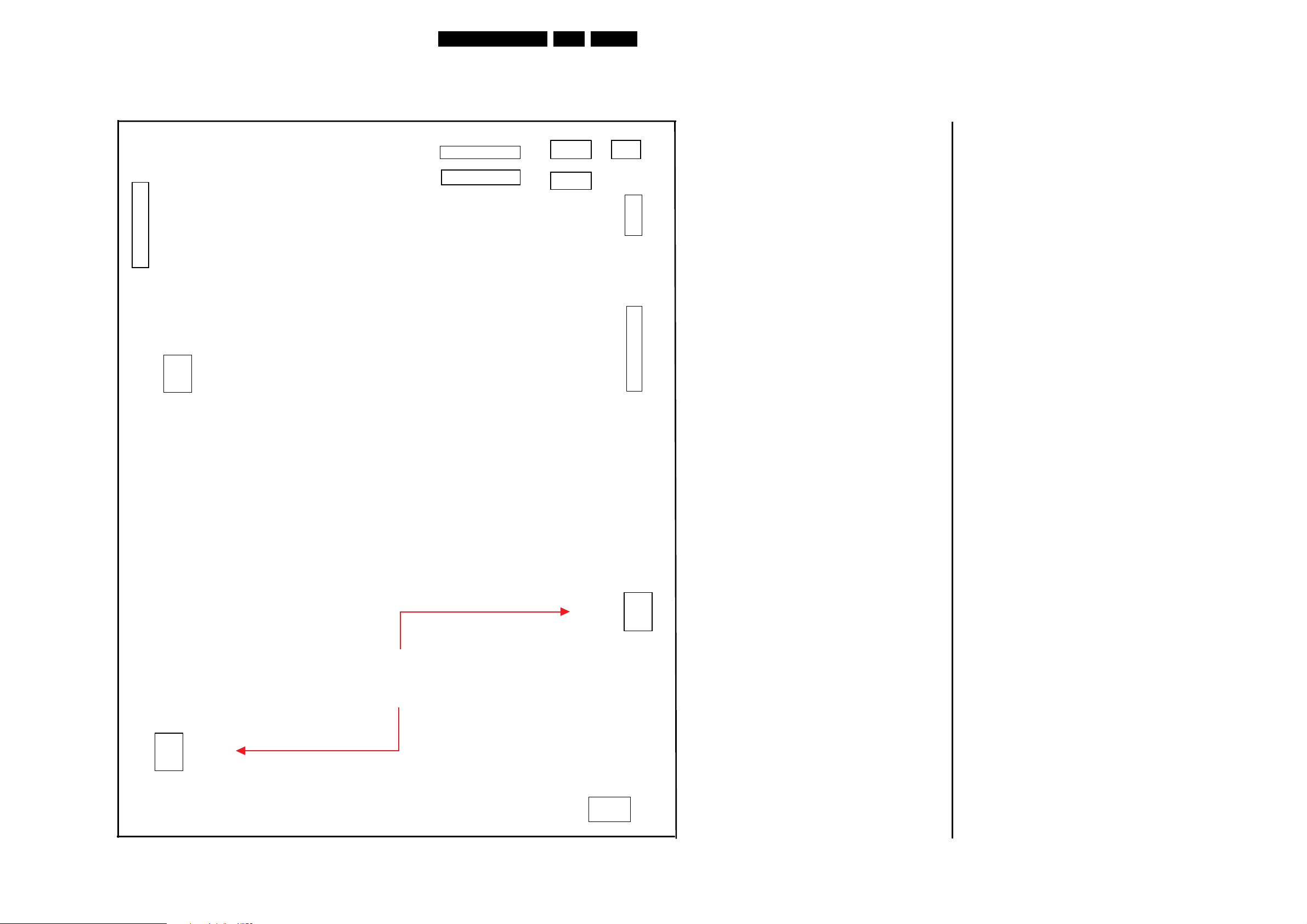
Block Diagrams, Test Point Overview, and Waveforms
1308 Mains connected. 1P10 Mains separated
1 VAC_Neutral 1 DIM-control
2 VAC_Live 2 Power Good
1M09: Mains separated
3 ON/OFF
1 +12Va 4GND
2 +12Va 5Boost (not used)
3 Gnd 6 nc.
4Gnd 7Standby
1M12: Mains separated
8 nc.
1 +12Va 9+5V2
2 +12Va 10 nc.
3 Gnd
1316/1319 Mains separated
4 Gnd 1 +24V
1P15: Mains separated
2 +24V
1 +12Va3+24V
2 NC 4 +24V
3 Gnd 5 +24V
6Gnd
7Gnd
8 Gnd
9Gnd
10 Gnd
11 Boost
12 ON/OFF
1 VAC_F_N 14 Gnd
2 VAC_F_L
1317/1321 Mains separated
1P22 Mains connected
1 +24V
2 GNDHOT 3 +24V
1 DIM-control 5 +24V
2 Power Good 6 Gnd
3 ON/OFF 7 Gnd
4Gnd 8 Gnd
5Boost (not used) 9 Gnd
6 Standby10Gnd
7 +5V2 11 Boost
8 +12Va 12 ON/OFF
Block Diagram Supply 47”
SUPPLY 47"- 52” SANKEN
55Q528.1A LA 6.
1P10
1
1P22
1
1317/1321
1316/1319
1
1
1M12
1M90
1M09
1P02
11
1P15
1
1
1P11
1
1M90 Mains separated
1 +12Va
2 +12Va
3 +12Va
4Gnd
5Gnd
6Gnd
1P02 Mains connected
1
+400V 2 +24V
13 DIM-control
1P02 and 1P02’ permit optima l cable routing
in different sets. They are connected in parallel
1
1P02
1308
1
1
1P11 Mains separated
4 +24V
H_16770_070.eps
230707

Block Diagrams, Test Point Overview, and Waveforms
Block Diagram Supply Audio & AmbiLight
AUDIO AND AMBIENT SUPPLY
AUDIO AND AMBIENTLIGHT SUPPLY
AP1
TO 1735
B11A
SSB
1P22
1P03
1
T2AH
2
DC INPUT
FROM
42” DISPLAY SUPPLY
AUDIO
AP2A
AP2B
1737
1
2
3
4
(ONLY FOR AUREA SET)
AUDIO: LEFT / RIGHT
AUDIO: PROTECTION MUTE / CONTROL
AUDIO-L
AUDIO-R
5P16
AUDIO-L
AUDIO-R
5P06
(ONLY FOR AUREA SET)
7P27
TEA1533AT
DRAIN
CONTROL
6
CTRL
2
VCC
DRIVER
9
ISENSE
DEM
7D38
7D00-3
14
11
7
6P16
2D19
2D17
3P40
3P33
IN-L
IN-R
3P73
3P27
5P25
STP6NK60ZFP
3P07
3P04
3P48
3P68
3P50
7P26
7D00-1
7D00-3
MUTE
AP2A
AP2A
AP2D
AP2D
5P07
7P02
5P03
3P78
CONTROL
LEFT-SPEAKER
RIGHT-SPEAKER
+SUB-SPEAKER
-SUB-SPEAKER
5P07
5P05
5P04
56Q528.1A LA 6.
AUDIO: LEFT / RIGHT
5P40
5P10
3
3
+12-15V
-12-15V
+12-15V
-12-15V
7D38
7D38
8
9
10
11
12
14
7P11
TCET1102
2
14
7P12
TCET1102
2
CONTROL
5P09
5P11
5P12
3P61
7P10
7D12
7D37
7DF3
5
3
2
1
7D10-1
7D10-2
CONTROL
7D35-1
7D35-2
CONTROL
6P10
6P13
6P12
K
A
R
CONTROL
5D00
5D25
CPROT
CPROT-SW
1P06
T5A
1P07
T5A
3P49
7P09
AUDIO-PROT
FEEDBACK-L
3D16
CPROT
5D03
LEFT-SPEAKER
FEEDBACK-R
3D16
CPROT
5D08
RIGHT-SPEAKER
3D19
AUDIO-PROT
3DH1
+3V3-STANDBY
5P20
5P19
2P12
3P05
AP2B
AP2B
AP2B
2D16
2D18
TO 1M59
AB09
DFI
+12-15V
-12-15V
+9VAL
1M59
1
SCL
2
3
SDA
4
SEL_0
5
SEL_1
NOT CONNECTED
FOR 1M80
SOUND-ENABLE
+3V3-STANDBY
5D04
5D07
1M80
1M81
1736
1735
1738
1
2
3
4
5
6
7
8
9
10
1
2
3
4
5
1
2
3
4
5
3
4
2
1
TO 1738
TO
AMBILIGHT
MODULE
SPEAKER L
SPEAKER R
B11A
SSB
AP2b,c,d
AP2b,c,d
AP2b
AP1
AP1
AP1
AP1
TO 1G50
B06A
SSB
AP2b
AP1
AP1
AP1
AP1
AP2A
VP1
+12-15V
AP2B
-12-15V
1738
1
AP2C
VP1
+12-15V
AP2D
-12-15V
5D05
5D06
AUDIO: PROTECTION / MUTE CONTROL
3DD0
AUDIO: SUBWOOFER
5D10
5D13
AUDIO: CENTRE INPUT / SW FILTER
VP1
VP
+12-15V
-12-15V-12-15V
VN
+12-15V+12-15V
VP1
-12-15V
+3V3-STANDBY
VP1
VP2
+12-15V
-12-15V-12-15V
VN2
+12-15V+12-15V
-12-15V
AP2a,c
AUDIO: CENTRE INPUT / SW FILTER
AP2D
AUDIO-L
AUDIO-R
7D40-1
7D40-2
AP2C
2D88
AUDIO:
SUBWOOFER
OUT-L
IN+SW
OUT-R
2D87
IN-SW
MUTE
7DK1-1
7DK1-2
+12-15V
7DK0-1
7DK0-2
CONTROL
-12-15V
+12-15V
7DL0-1
7DL0-2
CONTROL
-12-15V
7DK3
7DL2
3DK8
5D14
3DK9
5D15
FEEDBACK+SW
CPROT-SW
+SUB-SPEAKER
FEEDBACK-SW
CPROT-SW
-SUB-SPEAKER
AP2B
AP2B
2D86
2D84
1741
1
2
3
4
SUBWOOFER L
SUBWOOFER R
H_16801_118.eps
101007
Block Diagrams, Test Point Overview, and Waveforms
Block Diagram Video
VIDEO
MAIN TUNER
B03B
1T04
TD1716F/IHXP
MAIN HYBRID
TUNER
11
IF-OUT2
10
IF-OUT1
3
RF-GAIN
8
XTAL_OUT
VTU
9
+5V-ON
B08D
HDMI
1B01
1
ARX2+
3
ARX2-
4
ARX1+
6
ARX1-
7
ARX0+
9
ARX0-
10
ARXC+
12
ARXC-
13
18 2
15
16
19
ARX-HOTPLUG
1B02
1
BRX2+
3
BRX2-
4
BRX1+
6
BRX1-
7
BRX0+
9
BRX0-
10
BRXC+
12
BRXC-
13
18 2
15
16
19
BRX-HOTPLUG
1B03
1
CRX2+
3
CRX2-
4
CRX1+
6
CRX1-
7
CRX0+
9
CRX0-
10
CRXC+
12
CRXC-
13
18 2
15
16
19
CRX-HOTPLUG
HDMI SWITCH
ARX2+
ARX2-
ARX1+
ARX1-
ARX0+
ARX0-
ARXC+
ARXCBRX2+
BRX2-
BRX1+
BRX1-
BRX0+
BRX0-
BRXC+
BRXCCRX2+
CRX2-
CRX1+
CRX1-
CRX0+
CRX0-
CRXC+
CRXC-
ARX-DCC-SCL
ARX-DCC-SDA
7JE3
BRX-DCC-SCL
BRX-DCC-SDA
7JA3
CRX-DCC-SCL
CRX-DCC-SDA
7J28
7J27
AD8191ASTZ
74
73
71
70
68
67
65
64
12
11
9
8
6
5
3
2
24
23
21
20
18
17
15
14
HDMI 1
CONNECTOR
19
HDMI 2
CONNECTOR
HDMI 3
CONNECTOR
B08E
1
19
1
1
19
TUN-AGC
4-MHz
PCEC-HDMI
HOT-PLUG
PCEC-HDMI
HOT-PLUG
PCEC-HDMI
HOT-PLUG
HDMI
SWITCH
5T61
B04A
B04H
B04A
B04H
B04A
B04H
OP0
ON0
OP1
ON1
OP2
ON2
OP3
ON3
1T65
1
2
SAW 38MHz9 Audio AP
1T55
1
2
SAW 37MHz67 Analogue video
1T70
1
2
SAW 38MHz Audio + Dig.
B09A
AV1
AV2
AV3
D
34
33
37
36
40
39
43
42
RESET-SYS-DETECT
44
IF-FILTN3
4
5
IF-FILTP3
IF-FILTN1
4
5
IF-FILTP1
IF-FILTN2
4
IF-FILTP2
5
ANALOGUE EXTERNALS
1008
PR
PB
Y
1006
VIDEO
1007
1
3
5
S VIDEO
VIDEO
PR
PB
Y
1011
1009
4
2
SIDE I/O MS7
1302
VIDEO
1301
1
3
5
S VIDEO
2
4
B04E
7T57
TDA9898HL
4
IF3-B
3
IF3-A
7
IF1-B
6
IF1-A
PROCESSING
10
IF2-B
9
IF2-A
47
TAG C
46
FREF
AGC-DIN
FRONT_Y_CVBS_IN
CVBS
IF
OUT1-A
OUT1-B
MPP-2
AV1_PR
AV1_PB
AV1_Y
AV1_Y-CVBS
AV1_C
AV2_Y-CVBS
AV3_PR
AV3_PB
AV3_Y
FRONT_C_IN
RXC+
RXC-
RX0+
RX0-
RX1+
RX1-
RX2+
RX2-
57Q528.1A LA 6.
PNX85xx
B04
7T55
EF
33
TDA-IF-IN-N
26
TDA-IF-IN-P
27
CVBS4
3T59
3T58
IF-N
IF-P
7H00
PNX8537E/M2A
B04K
J3
M1
M2
K2
ADC/MUX/SRC
P5
F2
H2
N4
J1
K3
R1
G1
ANALOGUE AV
SWITCH/
PNX85xx
CONTROLLER
MSP
VMPG
MPEG
DEMUX
AND
DECODING
VIDEC, 3D COMB AND VBI
CAPTURING
MAIN
VIDEO OUT
VIDEO
LAYER
GFX LAYER
STILL
MPEG/PC
CPIPE-TV
GFX OSD
LAYER
MBVP-TV
SNR/TNR
EDDI
HV SCALER
MEMORY
DIGITAL
B04O
VIDEO OUT
LVDS
VIDEO
OUTPUT
CONFIG
LVDS
TRANSMITTER
CONTROL
B04F
PCI XIO
SDRAM
B04G
DDR
AG15
AH15
PCI --> NAND
B09B
1304
1M36
2
2
4
4
FRONT_Y-CVBS
FRONT_C
B08D
HOT-PLUG
J2
P2
B04H
D10
A10
A9
B7
HDMI-DVI RX/RX2DTL
B6
DETECTION
MATRICING
A8
A7
B9
B8
DIGITAL VIDEO
IN
RECEIVER
PNX5050: VIDEO
B05C
10-bit YUV 10-bit RGB
DV-Y(0-9)
DV-UV(0-9)
DV-HS
DV-VS
PNX85xx: FLASH
B04Q
7HA0
NAND512W3A2BN6E
AC14
AF12
7C00
PNX5050EH/M1
PNX5050
NAND
FLASH
128Mx8
PNX 85xx: SDRAM
B04G
DDR2-D(0-15)
DDR2-A(0-12)
(0-12)
(16-31)
7HG0
EDE2516ABSE
7HG1
EDE2516ABSE
AB02
1F50
1
2
3
4
10
11
12
13
14
15
17
18
20
21
22
23
25
26
27
28
39
30
32
33
35
36
37
38
40
41
AB07
DDR2
SDRAM
4Mx16x4
DDR2
SDRAM
4Mx16x4
VIDEO FLOW
+12V-SSB
SCL-I2C4-SSB
SDA-I2C4-SSB
DDR A
RXEA-
RXEA+
RXEB-
RXEB+
RXEC-
RXEC+
RXECLKRXECLK+
RXED-
RXED+
RXEE-
RXEE+
RXOA-
RXOA+
RXOB-
RXOB+
RXOC-
RXOC+
RXOCLK-
RXOCLK+
RXOD-
RXOD+
RXOE-
RXOE+
7CA2
EDD1216AJTA
DDR
SDRAM
2Mx16
7CA3
EDD1216AJTA
DDR
SDRAM
2Mx16
(0-11)
DQ1(0-15)
MM1-A(0-11)
(16-31)
AB06
C2
C1
D4
D3
D2
D1
E2
E1
E4
E3
F2
F1
G5
G6
H4
G3
H2
H1
L2
L1
J2
J1
H6
H5
RxP3_R(0-9)
RxP3_G(0-9)
RxP3_B(0-9)
RxP3R(0-5)
PNX5050: SDRAM
B05B
(0-12)
MM_DATA(0-15)
MM-A(0-12)
(16-31)
FPGA DFI
7F18
EP2C35F484C7N
CYCLONE II
FPGA
DFI
7CA0
EDD1216AJTA
DDR
SDRAM
16Mx16
7CA1
EDD1216AJTA
DDR
SDRAM
16Mx16
AB02
AB05
nSCO
C3
L6
C4
ASDO
AB03
W4
B12
AB08
DQ2(0-15)
MM2-A(0-11)
DCLK
SS-OFF
CLK-SYSTEM-SS
(0-12)
(16-31)
PACIFIC 3
B06C
7GE2
T6TF4HFG
PACIFIC3
ENHANCEMENT
VIDEO FLOW
FPGA: POWER +
CONTROL
7F30
EPCS16SI16N
7
SCD
16
15
CLOCK
7F51
1
EOH
3
OUT
50M
DDR B
7CA0
EDD1216AJTA
DDR
SDRAM 1
2Mx16
7CA1
EDD1216AJTA
DDR
SDRAM 2
2Mx16
PICTURE
75
74
78
77
81
80
84
83
87
86
90
89
93
92
96
95
99
98
101
100
103
102
107
106
SDA-I2C4-DISP
SCL-I2C4-DISP
VDISP
B06A
DUAL LVDS ONLY
TXEA-
TXEA+
TXEB-
TXEB+
TXEC-
TXEC+
TXECLK-
TXECLK+
TXED-
TXED+
TXEE-
TXEE+
TXOA-
TCOA+
TCOB-
TCOB+
TCOC-
TCOC+
TCOCLK-
TCOCLK+
TCOD-_
TCOD+
TCOE-
TCOE+
7GE1
M25P05
512K
FLASH
1F52
32
1
1F51
49
50
40
9
5
4
3
2
1
PACIFIC 3: LVDS
VDISP
5G00
5G01
5G02
5G03
5G04
5G05
5G06
5G07
5G08
5G09
5G10
5G11
LVD S
CONNECTOR
TO DISPLAY
LVD S
CONNECTOR
TO DISPLAY
1G50
41
40
39
38
32
31
30
29
28
27
25
24
22
21
20
19
17
16
15
14
13
12
10
CONNECTOR
9
7
6
5
4
LVDS
TO DISPLAY
OR
Only for 100Hz Dynamic Frame Insertion
H_16790_066.eps
220807

Block Diagrams, Test Point Overview, and Waveforms
Block Diagram Audio
AUDIO
MAIN TUNER
B03B
1T04
TD1716F/IHXP
MAIN HYBRID
TUNER
11
IF-OUT2
10
IF-OUT1
3
RF-GAIN
8
XTAL_OUT
VTU
9
+5V-ON
B08D
HDMI
1B01
1
ARX2+
3
ARX2-
4
1
19
HDMI 1
CONNECTOR
1
19
HDMI 2
CONNECTOR
1
19
HDMI 3
CONNECTOR
ARX1+
6
ARX1-
7
ARX0+
9
ARX0-
10
ARXC+
12
ARXC-
18 2
13
15
ARX-DCC-SCL
16
ARX-DCC-SDA
19
ARX-HOTPLUG
1B02
1
BRX2+
3
BRX2-
4
BRX1+
6
BRX1-
7
BRX0+
9
BRX0-
10
BRXC+
12
BRXC-
18 2
13
15
16
19
BRX-HOTPLUG
1B03
1
CRX2+
3
CRX2-
4
CRX1+
6
CRX1-
7
CRX0+
9
CRX0-
10
CRXC+
12
CRXC-
18 2
13
15
16
19
CRX-HOTPLUG
7JE3
BRX-DCC-SCL
BRX-DCC-SDA
7JA3
CRX-DCC-SCL
CRX-DCC-SDA
7J28
TUN-AGC
4-MHz
PCEC-HDMI
HOT-PLUG
PCEC-HDMI
HOT-PLUG
PCEC-HDMI
HOT-PLUG
5T61
B04A
B04H
B04A
B04H
B04A
B04H
1
2
1
2
1
2
1T65
SAW 38MHz9 Audio AP
1T55
SAW 37MHz67 Analogue video
1T70
SAW 38MHz Audio + Dig.
B09A
AV1
AV2
AV3
B08C
D
B08F
IF-FILTN3
4
5
IF-FILTP3
IF-FILTN1
4
5
IF-FILTP1
IF-FILTN2
4
IF-FILTP2
5
USA EXTERNALS
1006
AUDIO IN
L+R
1011
AUDIO IN
L+R
1060
AUDIO IN
1061
L+R
EXTERNALS
1C00
AUDIO OUT
L+R
1C01
AUDIO IN
L+R
1C03
DIGITAL
AUDIO
SIDE FACING SIDE AV
1302
AUDIO IN
L+R
HDMI SWITCH
ARX2+
ARX2-
ARX1+
ARX1-
ARX0+
ARX0-
ARXC+
ARXCBRX2+
BRX2-
BRX1+
BRX1-
BRX0+
BRX0-
BRXC+
BRXCCRX2+
CRX2-
CRX1+
CRX1-
CRX0+
CRX0-
CRXC+
CRXC-
(BACK)
(BOTTOM)
7J42
CONTROL
7T57
TDA9898HL
4
IF3-B
3
IF3-A
7
IF1-B
6
IF1-A
PROCESSING
10
IF2-B
9
IF2-A
47
TAG C
46
FREF
AGC-DIN
CVBS
IF
OUT1-A
OUT1-B
MPP-2
AUDIO-IN1-L
AUDIO-IN1-R
AUDIO-IN2-L
AUDIO-IN2-R
AUDIO-IN3-L
AUDIO-IN3-R
AUDIO-OUT-L
AUDIO-OUT-R
A-PLOP
AUDIO-IN4-L
AUDIO-IN4-R
SPI-OUT
L_FRONT_IN
R_FRONT_IN
7J27
AD8191ASTZ
74
73
71
70
68
67
65
64
12
11
9
8
6
5
3
2
24
23
21
20
18
17
15
14
33
26
27
B04M
SPI
HDMI
SWITCH
TDA-IF-IN-N
TDA-IF-IN-P
1304
34
OP0
33
ON0
37
OP1
36
ON1
40
OP2
39
ON2
43
OP3
42
ON3
44
7T55
EF
B04I
B08B
1
12
B09B
1M36
6
6
8
8
RESET-SYS-DETECT
14
8
7J30
7HM1
CVBS4
AUDI O
SPDIF
1
3T59
3T58
58Q528.1A LA 6.
PNX85xx
B04
IF-N
IF-P
11
ADAC(5)
ADAC(6)
12
SPDIF-IN1
4
SPDIF-OUT
11
AUDIO-IN5-L
AUDIO-IN5-R
RXC+
RXC-
RX0+
RX0-
RX1+
RX1-
RX2+
RX2-
B04E
7J00
PNX8537E
B04K
J3
M1
M2
B04L
AJ6
AK6
AF5
AG5
AH5
AJ5
AJ10
AK9
AK5
AH4
AK15
AJ15
AJ4
AK4
B04H
A10
A9
B7
HDMI-DVI RX/RX2DTL
B6
A8
A7
B9
B8
ANALOGUE AV
AUDIO
DIGITAL VIDEO
IN
RECEIVER
DETECTION
MATRICING
PNX85xx
ADC
DEMDEC
Delayed
SPDIF DECODING,
MULTICHANNEL,
DOWNMIX AND SRC
SPDIF OUT
DELAYED
Main
Main
CONTROL
B04F
PCI XIO
SDRAM
B04G
DDR
AUDIO
B04L
AJ13
DAC
AK12
I²C
MEMORY
CONTROL
B04O
B04A
EPICS
DAC
DIGITAL VIDEO
OUT / LVDS
STANDBY
CONTROLLER
DAC
AH16
V3
AH11
AH10
B04Q
PCI --> NAND
B04G
DDR2-D(0-15)
DDR2-A(0-12)
(16-31)
B04I
ADAC(1)
ADAC(2)
P0.7
ADAC(3)
ADAC(4)
PNX85xx: FLASH
7HA0
NAND512W3A2BN6E
NAND
FLASH
128Mx8
PNX 85xx: SDRAM
7HG0
K4D551638F
(0-12)
7HG1
K4D551638F
PNX 85xx:
AUDIO
9HM1
9HM2
B08C
DDR
SDRAM 1
8Mx16x4
DDR
SDRAM 2
8Mx16x4
AUDIO LEFT / RIGHT
B11A
MUTE
7D00-2
7D00-3
MUTE
AUDIO-RESET
7HV0
TPA4411RTJ
18
HEADPHONE
13
15
DRIVER
+AUDIO-L
FEEDBACK
-AUDIO-R
FEEDBACK
AUDIO: PROTECTION/MUTE CONTROL
B11C
PNX85xx: STANDBY CONTROLLER
B04A
PNX85xx: DEBUG
B04B
B04M
9H27
PNX 85xx: AUDIO
7HVA
A-PLOP
7HV1
A-PLOP-HDPH
+AUDIO-POWER
7D10-1
7D10-2
CONTROL
-AUDIO-POWER
+AUDIO-POWER
7D35-1
7D35-2
CONTROL
-AUDIO-POWER
7D63÷7D64
CONTROL
DV-B3_AUDIO-MUTE
AUDIO-RESET
ANALOGUE EXTERNALS
B09B
AUDIO-HDPH-L-AP
9
11
AUDIO-HDPH-R-AP
5D00 5D10
5DO7
5D11
DC-SENCE
AUDIO-MUTE
N.C.
1M36
10
11
7
LEFT-SPEAKER
LEFT-SPEAKER
RIGHT-SPEAKER
RIGHT-SPEAKER
7D70
7D00-1
7D00-4
SIDE FACING SIDE AV
D
1304
HEAD_PH_L
10
11
HEAD_PH_R
7
DETECT
CONTROL
AUDIO-PROT
B01A
1303
2
3
4
1735
1
2
3
4
H_16790_067.eps
Speaker L
Speaker R
Headphone
Out 3.5mm
220807
Block Diagrams, Test Point Overview, and Waveforms
Block Diagram Control & Clock Signals
CONTROL + CLOCK SIGNALS
B05B
PNX5050: SDRAM
B05A
PNX5050: CONTROL
E
KEYBOARD CONTROL
ON / OFF
CHANNEL +
CHANNEL -
VOLUME +
VOLUME -
J
LED PANEL
+5V2_STANDBY
+5V2_STANDBY
+5V2_STANDBY
+5V2_STANDBY
MENU
CONNECTOR
POWER SUPPLY
1016 (1706)
1011 (1703)
1012 (1704)
1015 (1702)
1014 (1701)
1013 (1705)
6010
(6051)
6011
(6052)
7010
(1040)
7013
(7070)
LIGHT
SENSOR
4 3 21
USB 2.0
TO
LED1
BLUE
LED2
RED
IR
SENSOR
7CA0
K4D551638F
7CA1
K4D551638F
DDR
SDRAM 1/2
16Mx16
EN_PCI_ARb
0 : DISABLES
1 : ENABLES
MEM_SIZE
1 0 0 : 32MB Product SW
1 0 1 : 64MB Assert SW
1 1 0 : 128MB Assert SW
CAS_LATENCY
0:2.5 CLKS
1:3 CLKS
ROM_WIDTH
HC_FASTMODE
0:8-Bit ROM /100kHz
1:16-Bit ROM/400kHz
BOOTMODE
1 0 : HOST ASSISTED
1 1 : EEPROM
B10B
USB 2.0
7N30
RYC8620
8
1H01
1
2
USB20-1-DM
3
4
B01B
1P11
7012
(7051)
1
2
3
5
6
USB20-1-DP
SUPPLY
BACKLIGHT-OUT
POWER-OK-DISPLAY
LAMP-ON-OUT
BACKLIGHT-BOOST
STANDBY
7011
(7061)
+5V2_STANDBY
7014
(7070)
OUTA
MM_DATA(0-31)
MM_A(0-12)
46
MM_CLK_N
MM_CLK_P
45
BOOTMODE7
BOOTMODE6
BOOTMODE5
BOOTMODE4
BOOTMODE3
BOOTMODE2
BOOTMODE1
BOOTMODE0
1
ENA_
2
FLGA
3
FLGB
4
ENB_
KEYBOARD
LED1
LED2
LIGHT_SENSOR
RC
7C00
PNX5050EH/M1
M1
M2
AC18
AD23
AF26
AF25
A4
A3
B3
B4
USB20-PWE1
USB20-PWE2
B06B
B06B
N.C.
B05B
B05A
B05C
1M01
1M01
1M20
(1M22)
SDRAM
PNX5050
CONTROL
VIDEO
B10A
B04E
B04D
2
2
B10C
7
6
4
3
1
D11
27M
1C05
D9
PCI-CLK-PNX5050_CLK-MOP
E23
D18
A11
RESET-SYS-DETECT
C7
F23
D24
H23
D26
H16
PCI-REQ-PNX5050
PCI-GNT-PNX5050
PCI-REQ-USB20
PCI-GNT-USB20
DV-CLK
USB 2.0
USB20-OC1
USB20-OC2
PCI-CLK-USB20
RESET-USB20
RESET-SYS-DETECT
PNX 85xx: MISCELLANEOUS
POD-MODE
B04A
ON-MODE
B04A
+3V3-STANDBY
3HD3
LED PANEL CONNECTOR
1M20
7
6
4
3
1
LED1
LED2
RxP3CLK
7N00
ISP1564HL
79
78
PCI
HOST
87
CONTROLLER
88
7
83
85
5
B04E
B01A
SUPPLY
CONTROL
7HD0
NCP303LSN
RST
2
IN
3
GND
KEYBOARD
LIGHT-SENSOR
B04E
B06C
B04E
STANDBY
1
RC
59Q528.1A LA 6.
B04
PNX 85xx:
7H00
PNX8537E
SDRAM
B04G
VIDEO STREAMS
B04N
PNX8535
CONTROL
B04F
CONTROL
PCI-AD(0-31)
ALE
AK17
B04O
B04F
D21
E21
E22
E20
B04A
Y1
EA
RC
AA4
AC1
AE2
AB4
AB2
AA3
AC3
AC2
AF2
AF1
AF4
AA1
AA2
AF3
Y2
Y3
W1
W4
U5
DC-VLK
B04F
PNX85xx: CONTROL
PCI-AD(0-31)
PCI-REQ-PNX8535
9H01
9H02
SDM
9H03
9H08
SPI-PROG
DETECT-1V2-2V5-3V3
DETECT-5V-12V (P2.5)
PCI-GNT-PNX8535
PCI-REQ-USB20
PCI-GNT-USB20
PSEN
SDM
SPI-PROG
CEC-HDMI
RESET-STBY
RESET-SYS-DETECT
AV1-BLK (P2.2)
AV2-BLK
AV1-STATU S
AV2-STATU S
KEYBOARD
LED1-3V3 (P0.0)
LED2-3V3
LIGHT-SENSOR
9
8
B04A
STANDBY CONTROLLER
B04B
B04B
B04B
7H22
7H21
CTRL3-STBY_POWER-OK-DISP (P2.7)
B08D
B04A
B04A
B04E
B09A
B09A
B09A
B09A
9H05
9H06
B04E
DIGITAL VIDEO
OUT / LVDS
CONTROL
STANDBY CONTROLLER
B04G
PNX 85xx SDRAM
7HG0
EDE2516ABSE
DDR2-D(0-15)
DDR2-A(0-12)
N28
DDR2-CLK_P
DDR2-CLK_N
N29
B04F
PNX 85xx: CONTROL
A21
AK26
AJ26
T2
U4
AG1
AG2
Y4
V5
AD1
AE4
AE3
AD4
AE1
AD3
U3
U2
U1
V4
V3
W3
W2
PCI-CLK-PNX8535
B04E
PNX 85xx: CONTROL
PCI-CLK-OUT
+3V3-PER
RESET-NVM_WP-NANDFLASH (P0.1)
27M
1HF0
CTRL4-STBY_SELECT-PWM-ANA (P2.6)
CTRL1-STBY_LAMP-ON (P0.5)
CTRL2-STBY_BACKLIGHT-CTRL_RESET-P3
REGIMBEAU_CVBS-SWITCH (P0.3)
7HG1
EDE2516ABSE
P2
P3
PCI-CLK-PNX5050-CLK-MOP
CTRL1-MIPS_LCD-PWR-ON
SPI-CLK
SPI-WP
SPI-CSB
SPI-SDO
SPI-SDI
ENABLE-1V2 (P0.2)
ENABLE-3V3 (P0.4)
AUDIO-RESET (P0.6)
UART-SWITCH (P0.7)
ON_MODE (P2.3)
POD-MODE (P2.4)
DDR
SDRAM 1/2
4Mx16x4
PCI-AD(24-31) --> NAND-AD(0-7)
PCI-CLK-DEBUG
PCI-CLK-PNX8535
PCI-CLK-USB20
RESET-SYS-DETECT
6HF0
7H02
M25P05-AVMN6P
6
512K
3
FLASH
1
5
2
B08A
B05A
B10A
B03A
B04B
B04B
B04B
BACKLIGHT-CONTROL
B02A B02C B04B
B09B
B04B
B04B
B02A
B04M
B04B
B04B B04C B08C
B02B B04B B04D
B05B B11A
B02A B02B B04B
B10A
B04A
B04D
B08F
B08F
HDMI SWITCH
RESET-SYS-DETECT
B04E
B04Q
PNX 85xx: FLASH
7HA3
RESET-NVM_WP-NANDFLASH-INV
B04C
PNX 85xx: NVM / UART SWITCH
7HC3
B06B
PACIFIC 3: DISPLAY
INTERFACING
CTRL-DISP1
CTRL-DISP4
LAMP-ON-OUT
BACKLIGHT-OUT
CTRL4-P3
7
7GE0
P87LPC761BDH
7GE1
M25P05-AVMN6P
6
3
1
5
2
1GE1
164
60M
165
B06C
178
168
172
7G53
CONTROL
PACIFIC 3
7GE2
T6TF4HFG
PACIFIC 3
7J27
AD8191ASTZ
HDMI
SWITCH
44
7HA0
NAND512W3A2BN6E
NAND
FLASH
(128Mx8)
7HC3
M24C64-WDW6P
8
EEPROM
(8Kx8)
RxP3CLK
7
MICRO
CONTROLLER
(AMBI LIGHT)
512K
FLASH
H_16790_068.eps
6
19
B06A
B06A
B01B
B01B
B06B
B05C
1GE0
10M
101007

Block Diagrams, Test Point Overview, and Waveforms
SSB: Test Points (Overview Top Side)
Part 1
H_16800_081a.eps
Part 2
H_16800_081b.eps
60Q528.1A LA 6.
I60 A5
I65 A5
I66 A5
I67 A5
I68 A5
I69 A5
I133 D4
I148 D3
I238 G2
I240 G2
I737 D4
I738 E2
I739 E3
I740 E2
I741 E2
I742 E3
I743 E1
I744 F2
I745 E2
I746 A5
I747 A5
I748 E2
I749 E2
I750 E2
IC50 B4
IC50 B4
IG64 A5
IG64 A5
IG69 A5
IG69 A5
IGB1 B5
IGB1 B5
IGB2 B5
IGB2 B5
IGE8 A5
IGE8 A5
IGF4 A5
IGF7 A5
IGF7 A5
IGF8 A5
IGF9 A5
IGH2 A5
IGH3 A5
IGH4 A5
IGH5 A5
IGH6 A5
IGH6 A5
IGH9 A5
IH06 E3
IH06 E3
IH09 E2
IH09 E2
IHD0 E2
IHDA F2
IHF4 E2
IHF4 E2
IHF8 E2
IHF8 E2
IHF9 E1
IHR0 E3
IHR3 E3
IHR3 E3
IHR4 E2
IHR4 E2
IHR5 E2
IHR5 E2
IHR6 E2
IHR9 E2
IHR9 E2
IHRA E2
IHRB E2
IHRC E2
IHRD E3
IHRF E3
IHRF E3
IHRG E2
IHS4 E2
IHS4 E2
IHS5 E2
IHS6 E2
IHS6 E2
IHVA E1
IHVA E1
IHW7 F1
IHW7 F1
IJ44 E1
IJ44 E1
IJ45 D1
IJ45 D1
IJ49 E1
IJ49 E1
IU69 D4
IU8E D4
IU91 D4
IU91 D4
3104 313 6194.3
H_16800_081.eps
030507

Block Diagrams, Test Point Overview, and Waveforms
SSB: Test Points (Part 1 Top Side)
61Q528.1A LA 6.
Part 1
H_16800_081a.eps
070507

Block Diagrams, Test Point Overview, and Waveforms
SSB: Test Points (Part 2 Top Side)
62Q528.1A LA 6.
Part 2
H_16800_081b.eps
030507
Block Diagrams, Test Point Overview, and Waveforms
63Q528.1A LA 6.
SSB: Test Points (Overview Bottom Side)
F50 G2
F41 E5
F32 E5
F23 C1
A1 E3
F5 A4
A2 G3
F6 A5
A3 G5
F7 A4
A4 G4
F8 A4
A5 G3
F9 A4
F1 A5
I1 A5
F2 A4
I2 A4
F3 B5
I3 A4
I4 A4
F4 A4
3104 313 6194.3
I5 B4
I6 A5
I7 A5
I8 A4
I9 B5
F10 A4
F11 A4
F12 A3
F13 A3
F14 A4
F15 A3
F16 A4
F17 D1
F18 D1
F19 C1
F20 C1
F21 C1
F22 C1
F24 C1
F25 C1
F26 C1
F27 E5
F28 D5
F29 D5
F30 D5
F31 C5
F33 C5
F34 F5
F35 F5
F36 C5
F37 E5
F38 E5
F39 E5
F40 E5
F51 G2
F42 E5
F52 F2
F43 E5
F53 G2
F44 C5
F54 G2
F45 E5
F55 G2
F46 F5
F56 E5
F47 G3
F57 C2
F48 G3
F58 C1
F49 G2
H_16800_082a.eps
Part 2
H_16800_082b.eps
F59 C1
F60 E2
F61 E2
F62 D1
F63 C1
F64 C2
F65 D2
F66 C2
F67 C2
Part 1
F68 C2
F69 C2
F70 D2
F71 E2
F72 E1
F73 E2
F74 E2
F75 E2
F76 E1
F77 D1
F78 E1
F79 D2
F80 E2
F81 E2
F82 D2
F83 E2
F84 E2
F85 E2
F86 E2
F87 E2
F88 E2
F89 E1
F90 D2
F91 F4
F92 F4
F93 F4
F94 F3
F95 F4
F96 F4
F97 F4
F98 F3
F99 F4
I10 A4
I11 B4
I12 A5
I13 A5
I14 A5
I15 A5
I16 A4
I17 A4
I18 A5
I19 B4
I20 B4
I21 A5
I22 A4
I23 A5
I24 A4
I25 B5
I26 A4
I27 E1
I28 F1
I29 F1
I30 E1
I31 E1
I32 D1
I33 D1
I34 D1
I35 E1
I36 F1
I37 F1
I38 E1
I39 F1
I40 E1
I41 D1
I42 C1
I43 D1
I44 D1
I45 D1
I46 E1
I47 E1
I48 C1
I49 E1
I59 E2
I50 C1
I61 D2
I51 E1
I62 E1
I52 C1
I63 E2
I53 G1
I64 E2
I54 B5
I70 E1
I55 C5
I71 D2
I56 C5
I72 C2
I57 E1
I73 C2
I58 E2
H_16800_082.eps
070507
I74 C2
I75 C2
I76 D2
I77 D2
I78 D2
I79 E1
I80 E2
I81 C2
I82 C2
I83 C2
I84 C2
I85 C2
I86 D2
I87 C2
I88 C2
I89 C2
I90 C2
I91 D2
I92 D2
I93 D2
I94 D2
I95 C2
I96 C2
I97 C2
I98 C2
I99 C2
AHF0 E3
AT6 2 G 3
AT6 3 G 3
AT6 4 G 4
AT6 5 G 5
F100 F4
F101 F4
F102 G4
F103 G4
F104 F4
F105 G4
F106 G4
F107 G5
F108 F5
F109 F5
F110 F5
F111 G5
F112 G5
F113 F5
F114 G5
F115 F3
F116 G5
F117 A3
F118 A3
F119 A4
F120 A4
F121 A4
F122 A4
F123 F5
F124 C5
F125 C5
F126 E5
F127 F5
F128 E5
F129 E5
F130 D5
F131 D5
F132 D5
F133 E5
F134 D5
F135 E5
F136 D5
F137 E5
F138 E5
F139 E5
F140 D5
F141 D5
F142 D5
F143 D5
F144 D5
F145 C5
F146 D5
F147 D5
F148 F4
F149 E3
F150 E3
F151 E3
F152 E4
F153 E4
F154 D4
F155 E4
F156 E4
F157 E4
F158 E4
F159 E3
F160 F3
F161 F3
F162 F4
F163 F3
F164 E4
F165 E4
F166 E4
F167 E2
F168 D3
F169 E3
F170 E3
F171 E4
F172 B3
F173 E3
F174 E4
F175 F4
F176 F4
F177 C3
F178 C3
F179 E4
F180 E5
F181 E5
F182 C3
F183 C3
F184 D3
F185 C3
F186 C3
F187 D3
F188 E3
F189 E3
F190 A1
F191 A1
F192 A1
F193 A1
F194 A1
F195 A1
F196 A1
F197 A1
F198 A1
F199 A1
F200 A1
F201 A1
F202 A1
F203 A1
F204 B1
F205 A1
F206 A1
F207 A1
F208 A1
F209 A1
F210 A1
F211 A1
F212 A1
F213 A1
F214 B1
F215 B1
F216 A1
F217 G2
F218 G3
F219 G3
F220 E3
F221 E3
F222 E3
F223 F2
F224 F2
F225 G1
F226 G1
F227 G1
F228 G1
F229 G1
F230 G1
F231 G3
F232 G3
F233 F3
F234 G3
F235 F3
F236 G3
F237 G1
F238 G3
F239 G2
F240 G2
F241 G2
F242 G2
F243 F2
F244 G2
F245 F2
F246 G2
F247 G2
F248 G3
F249 G3
F250 G3
F251 G3
F252 F1
F253 G3
F254 F2
F255 F2
F256 G3
F257 G2
F258 F3
F259 G3
F260 F3
F261 G2
F262 F2
F263 C1
F264 B1
F265 B1
F266 B1
F267 B1
F268 B1
F269 B1
F270 B1
F271 C1
F272 C1
F273 C1
F274 B1
F275 B1
F276 B1
F277 A2
F278 B2
F279 B2
F280 B2
F281 A2
F282 A2
F283 A2
F284 A2
F285 B2
F286 B2
F287 D1
F288 D1
F289 D1
F290 G1
F291 G1
F292 F1
F293 F1
F294 D1
F295 E1
F296 D1
F297 D1
F298 C1
F299 C1
F300 G1
F301 G1
F302 C1
F303 B1
F304 B1
F305 B1
F306 B1
F307 A1
F308 A1
F309 A1
F310 A1
F311 A1
F312 A1
F313 A1
F314 A1
F315 A1
F316 A1
F317 A1
F318 A1
F319 A1
F320 A1
F321 A1
F322 A1
F323 A1
F324 A1
F325 A1
F326 A1
FB20 C1
FB21 C1
FB22 C1
FB23 C1
FB24 C1
FB25 C1
FB26 C1
FB27 C1
FB28 C1
FB30 G1
FB31 G1
FB32 C1
FB33 C1
FB34 D1
FB35 D1
FB36 E1
FB37 D1
FB38 F1
FB39 F1
FB40 D1
FB41 D1
FB42 D1
FB43 D1
FB44 D1
FB45 G1
FB46 G1
FC00 B2
FC01 B2
FC10 A2
FC11 A2
FC12 A2
FC13 A2
FC14 B2
FC16 B2
FCA2 B2
FCA3 A2
FD00 B1
FD01 B1
FD02 B1
FD03 C1
FD04 C1
FD05 C1
FD19 B1
FD25 B1
FD26 B1
FD27 B1
FD28 B1
FD49 B1
FD64 B1
FD65 C1
FE57 F2
FE58 G2
FE60 F3
FE61 G3
FE62 F3
FE63 G2
FE64 G3
FE65 G2
FE66 F2
FE67 F2
FE68 G3
FE69 F1
FE70 G3
FE71 G3
FE72 G3
FE73 G3
FE74 G2
FE75 G2
FE76 G2
FE77 F2
FE78 G2
FE79 F2
FE80 G2
FE81 G2
FE82 G2
FE83 G2
FE84 G2
FE85 G3
FE86 F1
FE88 G3
FE89 F3
FE90 G3
FE91 F3
FEA0 G3
FEA1 G3
FEA2 G1
FEA3 G1
FEA4 G1
FEA5 G1
FEA6 G1
FEA7 G1
FEA8 F2
FEA9 F2
FEB0 E3
FEB1 E3
FEB2 E3
FEB3 F2
FEC1 G2
FEC2 G2
FEC3 G2
FEC4 G3
FEC5 G3
FEC6 G3
FEC7 G3
FEC9 G2
FG00 A1
FG01 A1
FG02 A1
FG03 A1
FG04 A1
FG05 A1
FG06 A1
FG07 A1
FG08 A1
FG09 A1
FG10 A1
FG11 A1
FG12 A1
FG13 A1
FG14 A1
FG15 A1
FG16 A1
FG17 A1
FG18 A1
FG19 A1
FG20 A1
FG21 A1
FG22 A1
FG23 B1
FG24 B1
FG25 B1
FG26 B1
FG50 A1
FG51 A1
FG52 A1
FG53 A1
FG54 A1
FG55 A1
FG56 A1
FG57 A1
FG58 A1
FG59 B1
FG60 A1
FGE0 A1
FGE1 A1
FGE2 A1
FGE3 A1
FGE4 A1
FGE5 A1
FGE8 A1
FGF2 A1
FGF3 A1
FGG0 A1
FGG1 A1
FGG2 A1
FGG3 A1
FH00 E3
FH01 E3
FH02 D3
FH10 C3
FH11 C3
FH12 D3
FHC1 C3
FHC2 C3
FHC3 E5
FHC4 E5
FHC5 E4
FHC6 C3
FHC7 C3
FHD0 F4
FHD1 E4
FHD2 E4
FHD4 E3
FHG0 B3
FHK0 E4
FHM0 E3
FHM1 E3
FHM2 D3
FHM3 E2
FHP0 E4
FHP1 E4
FHP2 E4
FHP3 E3
FHP4 F4
FHPA F3
FHPB F3
FHPE E3
FHR0 E4
FHR1 E4
FHR2 E4
FHR3 D4
FHR4 D4
FHR5 E4
FHR6 E4
FHV1 E3
FHV2 E3
FHV3 E3
FHV4 F4
FJ11 F5
FJ12 F5
FJ13 F5
FJ14 D5
FJ30 E5
FJ31 C5
FJ32 E5
FJ33 E5
FJ34 E5
FJ35 E5
FJ36 E5
FJ37 E5
FJ38 E5
FJ39 E5
FJ40 C5
FJ41 C5
FJ42 C5
FJ43 E5
FJ52 D5
FJA0 D5
FJA1 D5
FJA2 C5
FJA3 C5
FJA4 E5
FJA5 C5
FJA6 D5
FJA7 D5
FJB0 D5
FJB1 D5
FJB3 E5
FJB4 E5
FJB5 E5
FJB6 E5
FJB7 E5
FJB8 D5
FJB9 E5
FJC1 D5
FJC2 D5
FJC3 D5
FJC4 E5
FJC5 E5
FJEA F5
FJEB E5
FJEC C5
FJED C5
FJEE F5
FN00 A3
FN30 A4
FN31 A3
FN32 A4
FN33 A3
FN34 A4
FN35 A4
FN36 A4
FN37 A4
FN53 A4
FN54 A4
FN55 A4
FN56 A4
FN57 A4
FN58 A3
FN59 A3
FP00 A5
FP01 A4
FP02 A4
FP03 B5
FP04 A4
FP05 A5
FT11 G5
FT15 F3
FT17 G5
FT36 F5
FT37 F5
FT38 F5
FT39 F5
FT40 F5
FT41 F5
FT42 F5
FT50 G4
FT51 G4
FT56 F4
FT57 F4
FT58 G4
FT59 F4
FT60 F4
FT61 F4
FT62 F4
FT63 F4
FT64 F4
FT65 F4
FT66 F3
FT67 F4
FT68 F4
FT76 F4
FU00 D2
FU01 E1
FU02 E2
FU03 E2
FU04 E2
FU05 E2
FU06 E2
FU07 E2
FU08 D2
FU11 E2
FU12 E2
FU20 D2
FU21 E1
FU22 D1
FU23 E1
FU24 E2
FU25 E2
FU26 E2
FU27 E1
FU28 E2
FU29 D2
FU60 C2
FU61 C2
FU65 C2
FU66 C2
FU6S D2
FU80 C2
FU81 C1
FU82 D1
FU83 E2
FU84 E2
FU87 C1
FU88 C1
FU8A C2
I100 D2
I101 C2
I102 C2
I103 C2
I104 C2
I105 C2
I106 C2
I107 C2
I108 D2
I109 D2
I110 C2
I111 C2
I112 C2
I113 C2
I114 D2
I115 C2
I116 E2
I117 E2
I118 E2
I119 C2
I120 C2
I121 D2
I122 D2
I123 D1
I124 E1
I125 E2
I126 E2
I127 E1
I128 E2
I129 D2
I130 E1
I131 C2
I132 E2
I134 E4
I135 E3
I136 E4
I137 E3
I138 E3
I139 C3
I140 E3
I141 E3
I142 E3
I143 E3
I144 E3
I145 E3
I146 E3
I147 E3
I148 D3
I149 E3
I150 E3
I151 E3
I152 D3
I153 E3
I154 E3
I155 E3
I156 E3
I157 E3
I158 E3
I159 D2
I160 E2
I161 D2
I162 E2
I163 E2
I164 D2
I165 D2
I166 D2
I167 D2
I168 E2
I169 E2
I170 E2
I171 E1
I172 E1
I173 D1
I174 E1
I175 E1
I176 E2
I177 E2
I178 E2
I179 D1
I180 D1
I181 D2
I182 D2
I183 D2
I184 D2
I185 E2
I186 D2
I187 E2
I188 D1
I189 E2
I190 E2
I191 E1
I192 E1
I193 E2
I194 E2
I195 E2
I196 E2
I197 E2
I198 D2
I199 E2
I200 D2
I201 E2
I202 D2
I203 D1
I204 E2
I205 E2
I206 E2
I207 D1
I208 D2
I209 D2
I210 D2
I211 E2
I212 D1
I213 E2
I214 E2
I215 D2
I216 E1
I217 D2
I218 E2
I219 E2
I220 E2
I221 G4
I222 G4
I223 G4
I224 F4
I225 G4
I226 F4
I227 G5
I228 G5
I229 G4
I230 F4
I231 F4
I232 F4
I233 F4
I234 G4
I235 G3
I236 F4
I237 G4
I238 G4
I239 F4
I240 G4
I241 G4
I242 F4
I243 F4
I244 F4
I245 G5
I246 G5
I247 G5
I248 G5
I249 G5
I250 G5
I251 G5
I252 G5
I253 G5
I254 G5
I255 G5
I256 F4
I257 F3
I258 G5
I259 G5
I260 G5
I261 G5
I262 F5
I263 F5
I264 F4
I265 F4
I266 F5
I267 F5
I268 F5
I269 F5
I270 F5
I271 F5
I272 G5
I273 G5
I274 G5
I275 F5
I276 F5
I277 F4
I278 A3
I279 A3
I280 B4
I281 B4
I282 B4
I283 A4
I284 A3
I285 A4
I286 B4
I287 B3
I288 B3
I289 B4
I290 A3
I291 B3
I292 B4
I293 B3
I294 B4
I295 A4
I296 A4
I297 B4
I298 A3
I299 B4
I300 B3
I301 B4
I302 A4
I303 B4
I304 E5
I305 E5
I306 C5
I307 C5
I308 C5
I309 D5
I310 E5
I311 E5
I312 D5
I313 D5
I314 D5
I315 D5
I316 E5
I317 D5
I318 C5
I319 C5
I320 C5
I321 C5
I322 C5
I323 C5
I324 C5
I325 C5
I326 B5
I327 C5
I328 F5
I329 C5
I330 E5
I331 C5
I332 E5
I333 C5
I334 E5
I335 C5
I336 C5
I337 E5
I338 E5
I339 E5
I340 D5
I341 E5
I342 D5
I343 D5
I344 E5
I345 D5
I346 C5
I347 E5
I348 C5
I349 C5
I350 C5
I351 B5
I352 E5
I353 E5
I354 E5
I355 E5
I356 E5
I357 D2
I358 F4
I359 D3
I360 D3
I361 D4
I362 D4
I363 C4
I364 D3
I365 D3
I366 D3
I367 D3
I368 D3
I369 D3
I370 D3
I371 D3
I372 F4
I373 D4
I374 D4
I375 D3
I376 C2
I377 F5
I378 F5
I379 F4
I380 E4
I381 E5
I382 E4
I383 D2
I384 D3
I385 E3
I386 E3
I387 D3
I388 D3
I389 D3
I390 D5
I391 D4
I392 C4
I393 D4
I394 D4
I395 D4
I396 D4
I397 D4
I398 E4
I399 D4
I400 E3
I401 E4
I402 D4
I403 E4
I404 E4
I405 D4
I406 E4
I407 D4
I408 D3
I409 E4
I410 E4
I411 E3
I412 E3
I413 E3
I414 E3
I415 E3
I416 E3
I417 E3
I418 E3
I419 D4
I420 E4
I421 D3
I422 E3
I423 E3
I424 E4
I425 E4
I426 E4
I427 D3
I428 F3
I429 D3
I430 C3
I431 C3
I432 C3
I433 C3
I434 C3
I435 C2
I436 C2
I437 C3
I438 C3
I439 C3
I440 C3
I441 C3
I442 D3
I443 D3
I444 D3
I445 D3
I446 D3
I447 C3
I448 E3
I449 C3
I450 D3
I451 C3
I452 D3
I453 E3
I454 D3
I455 E3
I456 C2
I457 D3
I458 D3
I459 D3
I460 E2
I461 E3
I462 C3
I463 D4
I464 D4
I465 D5
I466 D4
I467 D5
I468 C3
I469 C4
I470 D3
I471 C4
I472 D5
I473 C3
I474 D4
I475 D4
I476 D4
I477 C3
I478 E3
I479 E3
I480 E3
I481 E3
I482 E3
I483 E3
I484 C3
I485 C3
I486 C3
I487 C4
I488 C4
I489 E4
I490 E3
I491 E3
I492 E3
I493 E3
I494 A1
I495 A1
I496 B1
I497 A1
I498 B1
I499 B1
I500 B1
I501 B1
I502 B1
I503 A1
I504 A1
I505 A1
I506 B1
I507 B1
I508 A1
I509 B1
I510 A1
I511 B1
I512 B1
I513 B1
I514 B1
I515 B1
I516 B1
I517 A1
I518 A1
I519 A1
I520 A1
I521 A1
I522 A1
I523 A1
I524 A1
I525 A1
I526 B1
I527 B1
I528 A1
I529 B1
I530 B1
I531 B1
I532 A1
I533 B1
I534 B1
I535 B1
I536 B1
I537 B1
I538 B1
I539 A1
I540 A1
I541 A1
I542 A1
I543 A1
I544 A1
I545 A1
I546 A1
I547 A1
I548 A1
I549 A1
I550 A1
I551 A1
I552 A1
I553 A1
I554 A1
I555 A1
I556 B1
I557 B1
I558 B1
I559 B1
I560 B1
I561 G1
I562 G2
I563 G2
I564 F2
I565 F3
I566 F3
I567 F3
I568 F3
I569 F3
I570 E3
I571 E3
I572 F2
I573 E2
I574 F2
I575 F2
I576 G1
I577 G1
I578 G1
I579 G1
I580 F3
I581 F3
I582 F3
I583 F3
I584 G3
I585 G2
I586 G3
I587 G3
I588 G3
I589 G2
I590 G2
I591 G1
I592 F2
I593 F2
I594 G1
I595 G1
I596 G1
I597 G1
I598 G2
I599 G2
I600 G3
I601 G2
I602 G2
I603 G2
I604 G2
I605 G2
I606 G2
I607 G1
I608 G1
I609 G2
I610 G1
I611 F3
I612 G2
I613 G3
I614 G3
I615 F3
I616 F3
I617 G3
I618 G2
I619 B1
I620 B1
I621 B1
I622 B1
I623 B1
I624 B1
I625 B1
I626 B1
I627 B1
I628 B1
I629 B1
I630 B1
I631 B1
I632 B1
I633 B1
I634 B1
I635 B1
I636 B1
I637 B1
I638 B1
I639 B1
I640 B1
I641 B1
I642 B1
I643 B1
I644 B1
I645 B1
I646 B1
I647 B1
I648 B1
I649 B1
I650 C1
I651 B1
I652 B1
I653 B1
I654 B1
I655 B1
I656 B1
I657 B1
I658 C1
I659 B1
I660 B1
I661 C1
I662 B1
I663 B1
I664 B1
I665 B1
I666 B1
I667 C1
I668 B1
I669 B1
I670 B1
I671 B1
I672 B1
I673 B1
I674 B1
I675 B1
I676 B1
I677 B1
I678 B1
I679 B1
I680 B2
I681 B2
I682 B2
I683 B2
I684 B3
I685 B3
I686 B3
I687 B3
I688 B3
I689 B3
I690 B2
I691 B2
I692 B2
I693 A2
I694 B3
I695 B3
I696 B3
I697 B2
I698 B2
I699 B2
I700 B2
I701 B1
I702 A1
I703 D1
I704 E1
I705 D1
I706 E1
I707 E1
I708 D1
I709 E1
I710 E1
I711 E1
I712 D1
I713 E1
I714 E1
I715 E1
I716 D1
I717 E1
I718 E1
I719 E1
I720 E1
I721 E1
I722 E1
I723 E1
I724 E1
I725 E1
I726 E1
I727 E1
I728 E1
I729 F3
I730 G3
I731 G3
I732 G3
I733 G3
I734 G1
I735 G2
I736 G3
I751 F3
I752 G3
I753 F3
I754 G2
I755 G3
I756 G3
I757 G3
I758 G1
I759 G2
I760 G2
I761 B3
I762 B3
IB10 G1
IB11 C1
IB12 E1
IB13 C1
IB14 E1
IB15 C1
IB16 D1
IB17 D1
IB30 F1
IB31 E1
IB32 F1
IB33 F1
IB34 E1
IB35 E1
IB36 D1
IB37 D1
IB38 D1
IB39 D1
IB40 E1
IB41 D1
IB42 E1
IB43 F1
IB44 F1
IB45 E1
IB46 E1
IB47 E1
IB48 E1
IB49 E1
IB50 E1
IB51 E1
IB52 E1
IB53 E1
IB54 E1
IB55 E1
IB56 E1
IB60 D1
IB61 D1
IB63 E1
IB64 E1
IB65 E1
IB66 D1
IB67 D1
IB68 D1
IB69 E1
IB70 E1
IB71 E1
IB72 D1
IB73 E1
IB74 E1
IB75 D1
IB76 E1
IB77 D1
IB90 C1
IC00 A2
IC01 B2
IC04 B2
IC07 B2
IC43 B3
IC44 B3
IC47 B3
IC52 A2
IC53 B2
IC54 B2
IC55 B2
IC56 B3
IC57 B3
IC58 B3
IC59 B3
IC60 B3
IC61 B3
IC62 B3
IC70 A3
IC71 B2
IC72 B2
ICA0 B2
ICA1 B2
ID01 B1
ID02 B1
ID03 B1
ID04 B1
ID05 B1
ID06 B1
ID07 B1
ID08 B1
ID09 B1
ID10 B1
ID11 B1
ID12 B1
ID13 B1
ID14 B1
ID15 B1
ID16 B1
ID17 B1
ID18 B1
ID20 B1
ID21 B1
ID22 B1
ID23 B1
ID24 B1
ID25 B1
ID26 B1
ID27 B1
ID28 B1
ID29 B1
ID30 B1
ID31 C1
ID32 B1
ID33 B1
ID35 B1
ID36 B1
ID37 B1
ID38 B1
ID39 B1
ID40 B1
ID41 B1
ID42 B1
ID45 B1
ID46 B1
ID47 B1
ID57 B1
ID58 B1
ID59 B1
ID60 B1
ID61 B1
ID70 B1
ID72 B1
ID73 B1
ID75 B1
ID77 B1
ID78 B1
ID79 B1
ID80 B1
ID82 B1
ID84 B1
ID86 B1
ID87 B1
ID88 B1
IE01 F2
IE02 G2
IE03 G1
IE04 G3
IE05 G3
IE06 G3
IE07 G2
IE08 G2
IE09 G3
IE10 F3
IE11 G3
IE12 F3
IE13 G3
IE14 G2
IE15 G1
IE16 F3
IE17 F3
IE18 G3
IE19 G3
IE20 G3
IE21 G3
IE22 G3
IE23 G3
IE24 G2
IE25 F3
IE26 G1
IE27 G2
IE28 G1
IE29 G1
IE30 G2
IE31 G2
IE32 G2
IE33 G2
IE34 G2
IE35 G2
IE36 G3
IE37 G2
IE38 G2
IE39 G1
IE40 G1
IE41 G1
IE42 G1
IE43 F2
IE44 F2
IE45 G1
IE46 G2
IE47 G2
IE48 G3
IE49 G3
IE50 G3
IE51 F2
IE52 G3
IEA0 F3
IEA1 F3
IEA2 F3
IEA3 F3
IEA4 F3
IEA5 G1
IEA6 G1
IEA7 G1
IEA8 G1
IEA9 F2
IEB0 F2
IEB1 E2
IEB2 E2
IEB3 E3
IEB4 E3
IEB5 F3
IEB6 F3
IEB7 F3
IEB8 F3
IEB9 F3
IEC0 F2
IEC1 G2
IEC2 G2
IEC3 G1
IG50 B1
IG51 B1
IG52 B1
IG53 B1
IG54 B1
IG55 A1
IG58 A1
IG59 A1
IG60 A1
IG61 A1
IG62 A1
IG65 A1
IG66 A1
IG67 B1
IG68 A1
IG70 A1
IG71 A1
IG72 A1
IG73 A1
IG74 A1
IG75 A1
IG77 A1
IG78 A1
IG79 B1
IG80 B1
IG81 B1
IG82 B1
IG83 B1
IG84 B1
IG85 B1
IG86 B1
IG87 B1
IG88 B1
IG89 A1
IG90 B1
IG91 B1
IG92 A1
IG93 A1
IG94 A1
IG95 A1
IG96 A1
IG97 A1
IGA2 A1
IGA3 A1
IGA4 A1
IGA5 B1
IGA6 B1
IGA7 B1
IGA8 B1
IGA9 B1
IGB0 B1
IGB3 B1
IGE0 B1
IGE1 B1
IGE2 B1
IGE3 B1
IGE4 B1
IGE6 A1
IGE7 A1
IGE9 A1
IGF0 B1
IGF1 B1
IGF2 B1
IGF3 B1
IGF5 B1
IGF6 A1
IGH0 B1
IGH7 A1
IGH8 A1
IH00 D3
IH01 E3
IH02 E3
IH03 E3
IH04 E3
IH05 E3
IH07 D3
IH08 E3
IH10 E3
IH11 E3
IH12 E3
IH13 E3
IH14 E3
IH15 E3
IH16 E3
IH17 E3
IH18 E3
IH19 E3
IH20 E3
IH21 C3
IH25 E3
IH26 E3
IH30 E4
IH31 E3
IH32 E4
IH90 E3
IH91 E3
IH92 E3
IH93 E4
IHA0 C4
IHA1 B4
IHC0 C3
IHC1 C3
IHC2 C3
IHD2 E3
IHD4 E3
IHD5 E3
IHD6 E3
IHD7 E3
IHDE E3
IHF0 C3
IHF1 D4
IHF2 D4
IHF3 D4
IHF5 C3
IHF6 D5
IHF7 C4
IHG0 D3
IHG1 C4
IHG2 C3
IHK0 D5
IHK1 D4
IHK2 D5
IHK3 D4
IHK4 D4
IHM1 C3
IHM6 E3
IHM9 E2
IHMA D3
IHMB D3
IHMC D3
IHMG C2
IHMV D3
IHMW D3
IHMY E3
IHMZ D3
IHN0 C3
IHN3 D3
IHN4 C3
IHN6 D3
IHN8 C3
IHN9 D3
IHNA D3
IHNB D3
IHND D3
IHNE D3
IHNF C3
IHNG C3
IHNH C3
IHNJ C3
IHNK C3
IHP5 C2
IHP6 C2
IHP7 C3
IHP8 C3
IHP9 C3
IHPA C3
IHPB C3
IHPD D3
IHPF F3
IHPG D3
IHR1 E4
IHR8 E4
IHRE E4
IHRH E3
IHRJ E3
IHRK D3
IHRL E4
IHRM D4
IHRT E3
IHRU E3
IHRV E3
IHRW E3
IHRY E3
IHRZ E3
IHS0 E3
IHS1 E3
IHS2 E4
IHS3 E4
IHS7 D3
IHS8 C4
IHS9 E4
IHSA D4
IHSB D4
IHSC E4
IHSD D4
IHSE E4
IHSF E3
IHSG D4
IHSH D4
IHSK D4
IHSL C4
IHSM D4
IHSN D4
IHSP D4
IHSR C4
IHSS D4
IHST D5
IHSU D3
IHSV D3
IHSW D3
IHSX E3
IHSY E3
IHV0 C3
IHV1 D2
IHV3 D4
IHV5 E5
IHV6 E4
IHV7 F4
IHV9 F5
IHVB F5
IHVC C2
IHVD D3
IHVE D4
IHW0 D4
IHW8 F4
IHWA D3
IHWE D3
IHWJ D3
IHWL D3
IHWZ D3
IHY0 D3
IHY1 D3
IHY2 D3
IHY3 C4
IHY4 D4
IHY5 D4
IHY6 D3
IHY7 D3
IHY8 D3
IHY9 F4
IHYA D2
IJ30 E5
IJ31 E5
IJ32 E5
IJ33 E5
IJ34 E5
IJ35 B5
IJ36 C5
IJ37 C5
IJ38 C5
IJ39 E5
IJ40 C5
IJ41 D5
IJ42 E5
IJ43 D5
IJ46 C5
IJ47 E5
IJ48 D5
IJ50 E5
IJ51 E5
IJ52 E5
IJ53 C5
IJ54 C5
IJ55 E5
IJ56 C5
IJ57 E5
IJ58 C5
IJ59 C5
IJ60 E5
IJ61 C5
IJ62 F5
IJ63 B5
IJ64 B5
IJ65 C5
IJ66 B5
IJ67 C5
IJ68 C5
IJ69 C5
IJ70 C5
IJ71 C5
IJ72 C5
IJ73 C5
IJ74 C5
IJA0 D5
IJA2 E5
IJA4 E5
IJA5 D5
IJA6 C5
IJA7 C5
IJA8 E5
IJA9 E5
IJB3 E5
IJE1 C5
IJE3 B5
IJE4 C5
IJE6 E5
IJE9 E5
IN00 B4
IN01 A4
IN02 B4
IN03 B3
IN04 B4
IN05 A3
IN06 B4
IN07 A4
IN08 A4
IN09 B4
IN10 B3
IN11 B4
IN12 B3
IN13 A3
IN14 B4
IN15 B3
IN16 B3
IN17 B4
IN19 A4
IN30 A3
IN35 A4
IN50 B4
IN51 B4
IN52 B4
IN53 A3
IN54 A3
IP00 A4
IP01 A4
IP02 A4
IP03 A5
IP04 B4
IP05 B4
IP06 A5
IP07 A4
IP08 A4
IP09 A4
IP10 A5
IP11 A5
IP13 A5
IP14 A5
IP15 A5
IP18 B4
IP20 A4
IP50 B5
IP51 A4
IP52 A5
IP53 B5
IP54 A5
IP55 A5
IP56 B4
IP57 A4
IP58 A4
IT03 F4
IT05 F5
IT07 F5
IT08 G5
IT10 G5
IT11 G5
IT12 F5
IT14 F5
IT15 F5
IT16 F5
IT18 F5
IT22 F5
IT24 F4
IT25 F4
IT26 F5
IT27 F5
IT31 G5
IT32 G5
IT33 G5
IT36 F5
IT41 F3
IT42 F4
IT50 G5
IT51 G5
IT52 G5
IT53 G5
IT54 G5
IT55 G5
IT56 G5
IT66 G5
IT67 G5
IT68 G5
IT69 G5
IT70 F4
IT71 F4
IT72 F4
IT73 G4
IT74 G4
IT75 F4
IT76 F4
IT77 F4
IT78 F4
IT79 G3
IT81 G4
IT85 F4
IT86 F4
IT87 F4
IT88 F4
IT89 G4
IT90 G5
IT91 G5
IT92 F4
IT93 G4
IT94 F4
IT95 G4
IT96 G4
IT97 G4
IU00 E1
IU02 D2
IU03 E2
IU04 E2
IU05 E2
IU06 E2
IU07 E2
IU08 E1
IU09 D2
IU10 D2
IU11 E2
IU12 E2
IU13 E1
IU14 E1
IU15 C2
IU16 D2
IU17 E2
IU18 E2
IU19 D1
IU20 D2
IU21 D2
IU22 C2
IU23 D2
IU24 D2
IU25 D1
IU26 E2
IU27 E2
IU28 E2
IU29 D1
IU30 D2
IU31 E2
IU32 D2
IU33 D2
IU34 D2
IU35 E2
IU36 E2
IU37 D2
IU38 E2
IU39 E2
IU40 E2
IU41 E1
IU42 E1
IU43 D2
IU44 E1
IU45 E2
IU46 E2
IU47 D1
IU48 E2
IU49 D2
IU50 D2
IU51 E2
IU52 D2
IU53 D2
IU54 D2
IU55 D2
IU56 D1
IU57 C1
IU58 E2
IU59 E2
IU60 E2
IU61 E1
IU62 E1
IU63 D1
IU64 C2
IU65 E1
IU66 E1
IU67 E2
IU68 E2
IU6A C2
IU6E D2
IU6F D2
IU6J C2
IU6K C2
IU6L C2
IU6M C2
IU6N C2
IU6P C2
IU6R C2
IU6T C2
IU70 C2
IU71 C2
IU72 C2
IU73 E2
IU74 E1
IU75 E2
IU76 E2
IU77 E1
IU78 D1
IU79 D2
IU7B C2
IU7C C2
IU7E C2
IU7F D2
IU7H D2
IU7J D2
IU7K C2
IU7L C2
IU7M C2
IU7N C2
IU7P D2
IU7Q C2
IU7R C2
IU7T C2
IU7V C2
IU80 D2
IU81 C2
IU82 C2
IU83 E2
IU84 E2
IU85 E2
IU86 C2
IU87 D2
IU88 C2
IU89 C2
IU8A D2
IU8B D2
IU8C D2
IU8D C2
IU8F D2
IU8G C2
IU8H E2
IU8I E1
IU8J E2
IU90 D2
IU92 D2
IU93 D2
IU94 D2
IU95 E2
IU96 E2
IU97 D2
IU98 E2
IU99 D2

Block Diagrams, Test Point Overview, and Waveforms
0
SSB: Test Points (Part 1 Bottom Side)
64Q528.1A LA 6.
Part 1
H_1680
Block Diagrams, Test Point Overview, and Waveforms
SSB: Test Points (Part 2 Bottom Side)
65Q528.1A LA 6.
Part 2
H_16800_082b.eps
070507

I2C IC Overview
I²C
PNX8535: CONTROL
B04E
Block Diagrams, Test Point Overview, and Waveforms
HDMI SWITCH
B08F
+3V3-PER
B08D
HDMI
66Q528.1A LA 6.
B06C
PACIFIC 3
CHANNEL DECODER
B03A
B03B
MAIN TUNER
I2C3-SDA
I2C3-SCL
B04H
DDC-SDA
DDC-SCL
7H00
PNX8537E
PNX8535
ERR
05
B04F
PCI XIO
B04G
SDRAM
I2C2-SDA
I2C2-SCL
B04A
I2C uP-SDA
I2C uP-SCL
STANDBY
CONTROL
I2C1-SCL
B04O
VID_OUT
B0_UART
B1_UART
HDMI
ERR
53
RXD
TXD
I2C1SDA
RXD
TXD
TTL
AJ27
AJ28
E10
C9
AK28
AK29
AH3
AG4
U4
V3
AB1
AC5
AH27
AK27
E27
D28
AF15
AK16
SDA3
SCL3
ERR
03
PNX8535: DIGITAL VIDEO IN
B04H
PNX8535: FLASH
B04Q
7HA0
NAND512W3A
NAND
PCI-AD
B04G
DDR2-D
DDR2-A
FLASH
(128x8)
PNX8535: SDRAM
7HG0
EDE2516ABSE
7HG1
EDE2516ABSE
DDR2
SDRAM
4Mx16x4
SDA2
SCL2
PNX8535: STANDBY CONTROLLER
B04A
7H02
M25P05
512K
FLASH
P0.1
P0.7
SDA1
SCL1
PNX8535: DIGITAL VIDEO OUT / LVDS
B04O
3HPJ
3HPH
3HPG
3HPF
3H41
3H38
3H59
3H61
3HPE
3HPD
9HWH
9HWG
3HPK
3HPM
SDA-2
SCL-2
+3V3-STANDBY
3H02
3H03
SDA-SLAVE
SCL-SLAVE
SDA-SSB
SCL-SSB
DDC-SDA
DDC-SCL
9HP8
9HP6
9HP7
9HP5
3J29
50 49
7J27
AD8191ASTZ
HDMI
89
SWITCH
90
ERR
7HP5
PCA9540BDP
2 CHANNEL
I2C
MULTIPLEXER
3HPQ
2
3HPT
PNX5050: CONTROL
B05A
SDA-SSB
SCL-SSB
PNX8535: NVM / UART SWITCH
B04C
RESET-NVM_WP-NANDFLASH
ERR
1
SDA-UP-MIPS
SCL-UP-MIPS
UART-SWITCH
RXD-UP
TXD-UP
RXD-MIPS
TXD-MIPS
DV-B0_UART2-RX
DV-B1_UART2-TX
9T21
9T22
BIN-5V
3JA5
3JB5
3JA7
3JC0
56
M24C02
EEPROM
PNX5050: SDRAM
7CA0
EDD1216AJTA
7CA1
EDD1216AJTA
DDR
SDRAM
16Mx16
3JE3
13
R1-IN
3JE2
14
R2-IN
3JE5
8
3JE4
7
7JA1
3JB4
3JB6
RXD2
TXD2
CIN-5V
3JG3
3JG5
56
7J29
M24C02
EEPROM
PACIFIC 3: LVDS
B06A
SDA-I2C4-DISP
SCL-I2C4-DISP
MAIN TUNER
B03B
9T85
9T86
3JG2
ARX-DDC-SDA
ARX-DDC-SCL
BRX-DDC-SDA
BRX-DDC-SCL
CRX-DDC-SDA
CRX-DDC-SCL
3JH6
SDA-MUX2-BUF
SCL-MUX2-BUF
1HE2
3
UART2
2
FOR
FACTORY
1
USE ONLY
9J06
9J07
3G52
3G53
9T51
9T52
1B01
1B02
1B03
1G50
16
15
16
15
16
15
1
2
3x HDMI
CONNECTOR
LVD S
COONECTOR
TO DISPLAY
OR
3T77
76
1T04
TD1716F/IHXP
MAIN
TUNER
ERR
34
RXD-SERV
TXD-SERV
3T53
1
18 2
19
3GG2
198 200
7GE2
T6TF4HFG
PACIFIC 3
ERR
VIDEO-FLOW
AB02
1F50
41
SDA-I2C4-SSB
40
SCL-I2C4-SSB
Only for 100Hz
Dynamic Frame Insertion
UART
B08A
1M15
3J11
3
3J12
2
3GG3
62
61
68
69
AB09
7GE1
M25P05
FLASH
PWM-3
PWM-OR
DISPLAY
INTERFACING
3F19
3F20
UART
SERVICE
CONNECTOR
512K
7GE0
P87LPC764BDH
1
8
AB06
Dynamic Frame Insertion
MICRO
CONTROLER
FPGA DFI
3FA0
P2 P1
7F18
EP2C35F484C7N
CYCLONE II
(FPGA)
ERR
65
Only for 100Hz
3F49
PACIFIC 3: DISPLAY-INTERFACING
B06B
SDA-AMBI-3V3
18
SCL-AMBI-3V3
17
FPGA AMBILIGHT
AB10
3F9G
XC3S250E
4FTG256C(XILI)R
SPARTAN
Dynamic Frame Insertion
With AMBI-LIGHT
SDA-I2C4
SCL-I2C4
P11 R11
FPGA
Only for 100Hz
46
3JA1
3JC5
3JG7
3C51
AIN-5V
3JA6
3JA0
3JB0
3JG6
3JA8
56
7JA0
M24C02
EEPROM
B05B
MM_DATA
MM_A
7JE2
ST3232C
9
R2-OUT
T1-OUT
10
T2-IN
RS232
INTERFACE
T2-OUT
12
R1-OUT
11
T1-IN
UART
LEVEL ADAPTER
3J09
PARX-DDC-SDA
85
PARX-DDC-SCL
86
PBRX-DDC-SDA
93
94
98
99
4
5
7
8
ERR
ERR
7HC4
7HC1
PBRX-DDC-SCL
PCRX-DDC-SDA
PCRX-DDC-SCL
3HPS
3HPR
11
3HPU
3HPW
12
SDA-PNX5050
SCL-PNX5050
8
7HC0
74HC4066PW
2
9
3
10
+3V3-STANDBY
3HPY
+3V3-STANDBY
3HPC
56
7HC3
M24C64
EEPROM
(MAIN NVM)
5
4
1
8
11
3HPX
3HPZ
3HC3
3HC6
PACIFIC 3: DISPLAY-INTERFACING
B06B
SDA-SSB-MUX1
SCL-SSB-MUX1
SDA-SSB-MUX2
SCL-SSB-MUX2
PNX5050: VIDEO
B05C
3C50
C8 D8
7C00
PNX5050EH/M1
PNX5050
ERR
22
EXTERNALS
B08C
RXD
TXD
3JE1
3JE0
23
24
9C08
9C07
7F65
3FPH
SDA-SSB1
SCL-SSB1
7G61-2
+3V3
B4
A5
7G61-1
3F6J
3F9E
+5V-ON
3GA0
3GA3
DISPLAY INTERFACING
AB09
SDA-AMBI-3V3
SCL-AMBI-3V3
SUPPLY
B01B
SDA-AMBI
SCL-AMBI
7F09-2
Dynamic Frame Insertion
3T57
23 24
7T57
TDA9898HL
IF
PROCESSING
ERR
26
3B59
3B58
3F37
7F09-1
+3V3
Only for 100Hz
With AMBI-LIGHT
3T56
5B10
5B12
+5V
3F38
H_16790_069.eps
3F45
3B44
1M59
1M59
220807
3
1
3
1
TO
AMBI-LIGHT
MODULE
TO
AMBI-LIGHT
MODULE

Block Diagrams, Test Point Overview, and Waveforms
Supply Lines Overview
SUPPLY LINES OVERVIEW
SUPPLY
B01A
1P02
2
1
A
A
CONTROL
5
3
2
1
DISPLAY
SUPPLY
1P11
1M09
1M90
SEE ALSO BLOCK
DIAGRAM SUPPLY
2B48
5B01
6B07
7
2B51
8
6B08
9
6B06
10
2B46
11
6B05
12
2B51
7B50
3128
7B04
TCET1102
2143
1 1
2
3
4
5
6
7
8
1
TO 1M09
2
AMBI-LIGHT UNIT
3
OR DFI PANEL
4
1
2
3
TO 1M90
4
DFI PANEL
5
6
B01a
B02b
B02b
CONTROL
B01B
1P11
2
3
4
5
6
7
8
B02A
+12VS
+5V-POD
1V2-STANDBY
7U00
NCP5422
Out-of-Phase
Synchronous
Buck Controller
1B33
7B06
2.5AT
K
R
A
AUDIO-PROT
B11C
STANDBY
B04D
SEE ALSO BLOCK DIAGRAM SUPPLY
SUPPLY
BACKLIGHT-OUT
POWER-OK-DISPLAY
LAMP-ON-OUT
BACKLIGHT-BOOST
STANDBY
9B06
1B50
T3A
DC/DC
7U16
7U14
POD-MODE
5U00
7U01
3U01
15
1
Dual
7U06
2
7U03
16
7U08
15
6B15
3B72
12V/3V3
COVERTER
5U03
7U28
COVERTER
5U02
+AUDIO-POWER
-AUDIO-POWER
+12VS
3B73
+5V-STANDBY
3B29
B06B
B04A
B06B
N.C.
B04D
+5V-STANDBY
+12V-DISP
+12VS
+12V
+12VF
+3V3
+3V3F
+1V8
12V/1V2
+1V2
+5V-POD
1V2-STANDBY
7U27
STAB.
67Q528.1A LA 6.
PACIFIC 3: LVDS
B04p
B04e,f,k,n
B04h
B04o
B05d
B05a
B06A
VDISP
PACIFIC 3: DISPLAY-INTERFACING
B06B
+12V-DISP
7G54
+3V3-STANDBY
+3V3
+5V-ON
+12V
3GC4
PACIFIC 3
B06C
5GE2
7GE3
IN OUT
COM
7GE5
IN OUT
COM
UART
B08A
+3V3-STANDBY
SPDIF
B08B
+3V3
EXTERNALS
B08C
+3V3-STANDBY
7J50
7J51
UART-SWITCH
+3V3
+12V
HDMI
B08D
1B01
HDMI
18
CONNECTOR
1B02
HDMI
CONNECTOR
HDMI
CONNECTOR
+5VS
B08F
+5V-CON
+3V3
B09A
+5VS
+12V
3JC8
18
1B03
18
HDMI SWITCH
5JA5
5JA3
5JA4
ANALOGUE EXTERNALS
5G55
3JC7
3JH3
5GE0
5GE1
5GE3
5GE4
5GE5
5GE6
VDISP
+12V-DISP
VDISP
+3V3-STANDBY
+3V3
+5V-ON
+5V-STANDBY+5V-STANDBY
+12V
+8V2-PAS
+3V3+3V3
+3V3-P3
+2V5-PF
+2V5-P3
+2V5-PLL
+1V5
+1V5-P3
+1V5-PLL
+1V5-TX
+1V5-RX
+3V3-STANDBY
+3V3
+3V3-STANDBY
+3V3-UART
+3V3
+12V
AIN-5V
BIN-5V
CIN-5V
+5V-CON
+5VS
+5V-CON
+5V-MUX
+3V3
+3V3-DIG
+3V3-ANA
+5VS
+12V
1G50
B02a
41
TO 1F50
AB02
DIF
B02b
B06a
B02b
B01a
B01a
B02b
B02b
B11a
B11a
B11a
B11a
TO 1M20
B10C
SSB
TO 1M90
SUPPLY
TO 1G50
B06A
SSB
B08f
AB09
AB01
AB01
AB01
AB01
DC / DC
B02B
B01a,b
B11a
B11a
B02a,b,
B02b,B06b
B01a
B11a
B11a
B02a
B02a
B02a
B02a
B02a
B02b
B06b,B04o
B02a
B02a
B02b
B02b,c,
B04a,B06b,
B09a,b,B08c
B02a
B02b
B02b,c
B02b
B02b,c,B3a,b,
B04a,e,l,m,p,q
B05a,b,c,d,B06b,
c,B08b,c,f,B10a
1V8
B04p
B02b
B02a
B02a
B02b
B02b
B02b
B02b
B02b
B02b
B02b
B02a
B02a
B02c
B03a,B04e
+5V-STANDBY +5V-STANDBY
7U04-1
3U86
7U17
VOLT.
REG.
+12VS +12VS
VP VP
VN VN
+12V
+12VF
3UB3
VSW
DC / DC
B02C
+3V3F +3V3F
7U8B
VOLT.
REG.
+12V
+12VF
5U68
7U64
L6910
CHANNEL DECODER
B03A
+3V3
+1V2
+5V-ON
MAIN TUNER
B03B
+3V3
+5V-ON
VTUN
PNX85xx: STANDBY CONTROLLER
B04A
+3V3-STANDBY
+3V3
+2V5
+12V
+5V-ON
PNX85xx: DEBUG
B04B
+3V3-STANDBY
PNX85xx: NVM / UART SWITCH
B04C
+3V3-STANDBY
+5VS
PNX85xx: MISCELANEOUS
B04D
+3V3-STANDBY
+5VS
PNX85xx: CONTROL
B04E
+3V3-STANDBY
+3V3-PER
+3V3
+1V2
7U02-1
POD-MODE
7U19
5U09
7U24
7U8C
STEP
DOWN
CONTR
3U94
7U02-2
7U04-2
ON-MODE
7U20
7U18
VOLT.
REG.
6U63
7U61-1
15
11
7U61-2
14
5T08
5T08
5T53
3T66
3T67
7T50
3UB4
9U8A
5U60
5T52
+5VS
+5V-POD
+5V-ON
+3V3-STANDBY
+1V2-STANDBY
+12V
+12VF
+VTUN
(RESERVED)
+2V5
+12V
+12VF
+1V4
Only for Europe
+3V3
+3V3DVB
+1V2
+1V2DVB
+5V-ON
+3V3
+5V-ON
V1
VTUN
33VTUN
ANTENNA-SUPPLY
(RESERVED)
+3V3-STANDBY
+3V3
+2V5
+12V
+5V-ON
+3V3-STANDBY
+3V3-STANDBY
+5VS
+3V3-STANDBY
+5VS
+3V3-STANDBY
+3V3-PER
+3V3
+1V2
B04p
B04c,d,l,m
B09a,B10c
B02a
B02a
B03a,B04a,b,
B06b,B10b
B04a,b,c,d,e,m,p,
B06b,B08a,c,B11a,c
B02a,B04p
B04p
B11a
B11a
B04p
B02b
B02a
B04a,B05b
B02b
B02a
B02b
B04p
B01b
B04p
B02a
B02a
B02b
B02b
B02a
B04l
B02a
B02a
B05d
B02c
B02a
B02a
B02b
RES
B05b
PNX85xx: CONTROL
B04F
+3V3-PER
PNX85xx: SDRAM
B04G
+1V8
3HJ1
3HJ3
PNX85xx: DIGITAL VIDEO IN
B04H
RREF-PNX8535
PNX85xx: AUDIO
B04I
VP
5HM0
VN
5HM1
PNX85xx: ANALOGUE AV
B04K
+3V3-PER
PNX85xx: AUDIO
B04L
+5VS
B04M
+3V3-STANDBY
+3V3
+5VS
B04N
+3V3-PER
B04O
+12V-DISP
VDDA-LVDS
B04P
+1V2
+1V8
+3V3-STANDBY
+1V2-STANDBY
+3V3
VDDA-AUDIO
B04Q
+3V3
B05A
+3V3
+3V3-D
B05B
+2V5
B05C
+3V3
B05D
+3V3
+1V4
+2V5-DDR
7HP0
5HP1
IN OUT
COM
PNX85xx: AUDIO
PNX85xx: VIDEO STREAMS
PNX85xx: DIGITAL VIDEO OUT / LVDS
PNX85xx: POWER
5HYA
5HY4
5HY7
PNX85xx: FLASH
5HA0
PNX5050: CONTROL
PNX5050: SDRAM
5CA1
PNX5050: VIDEO
PNX5050: SUPPLY
5CD1
7HK0
IN OUT
COM
5HK2
5HY1
3CA1
3CA3
+3V3-PER
+1V8
DDR2-VREF-CTRL
DDR2-VREF-DDR
RREF-PNX8535
VP
AUDIO-VDD
VP
AUDIO-VEE
+3V3-PER
+5VS
VDDA-AUDIO
+3V3+3V3
+3V3-STANDBY
+3V3
+5VS
+3V3-PER
+12V-DISP
VDDA-LVDS
+1V2
+1V8
+3V3-STANDBY
+1V2-STANDBY
+3V3
+1V8-PNX
+3V3-PER
RREF-PNX8535
VDDA-LVDS
VDDA-AUDIO
VDDA-DAC
AUDIO-ADC
+3V3
+3V3-NAND
+3V3
+3V3-D
+2V5
+2V5-DDR
VREF-DDR
+2V5-STAB
+3V3
+3V3
+3V3-D
+1V4
+2V5-DDR
B06b
B01b
B02b
B02a
B02b
B02b
B02a
B02a
B02b
B02a
B02B
B02a
B02a
B02b
B08d
B02a
B02b
B02a
USB 2.0
B10A
+3V3
USB 2.0
B10B
+5V-ON
LED PANEL CONNECTOR
B10C
+5VS
AUDIO LEFT / RIGHT
B11A
+AUDIO-POWER
3D04
3D04
7D55
7D55
7D58
ON-MODE
7U08
IN OUT
COM
5F23
5F24
5F25
3U01
1U01
3.0AT
1U02
3.0AT
14
5F53
15
16
1
2
7D61
7U03-1
7U03-2
7U01-1
7U01-2
7U09
IN OUT
COM
ON-MODE
12V/1V2
COVERTER
5U02
12V/3V3
COVERTER
5U01
-AUDIO-POWER
3D39
+3V3-STANDBY
AUDIO: PROTECTION/MUTE CONTROL
B11C
+3V3-STANDBY
VP
VN
VPP
VNN
LED PANEL
J
1M20
+5V_STANDBY +5V_STANDBY
5
DC/DC
AB01
1M90
1
5U04
5U05
5U06
5U07
7U00
NCP5422
Dual
Out-of-Phase
Synchronous
Buck Controller
VIDEO-FLOW
AB02
1F50
1
+VDISP
PNX8535: CONTROL
AB03
+3V3
FPGA: POWER + CONTROL
AB05
+1V2
5F54
5F55
+2V5
+3V3
+3V3
+5V-ON
+5VS
+AUDIO-POWER
VPP
VP
VP
-AUDIO-POWER
VNN
VN
+3V3-STANDBY
+3V3-STANDBY
VP
VN
VPP
VNN
+12VS
+12V
+12V-DC
+1V2
+2V5
+3V3
+12V-SSB
+VDISP
+3V3
+1V2
+1V2-FPGA
+1V2-PLL
+2V5
+Vin-FPGA
+2V5out-FPGA
+2V5in-FPGA
+3V3
1M20
1F51
5
1
TO
DISPLAY
AB08
AB05
AB05
AB05
AB05
AB06
AB05
AB07
AB08
AB01
AB01
AB01
AB01
AB01
AB01
AB01
AB01
AB06
2V5-DDR2
+2V5out-FPGA
+Vin-FPGA
+1V2-FPGA
+1V2-PLL
2V5-DDR1
+2V5in-FPGA
VREF-FPGA2
TO 1M22
J
LED
+3V3
AB07
B11C
+2V5
B02b,B04i,
B11c
B11c
B02b,B04i,
B11c
AB08
+2V5
AB09
AB10
+3V3
AB09
+2V5
+1V2
AB05,AB10
AB05,AB07,AB08,AB10
AB03,AB05,AB06,AB09,AB10
AB06
AB06
AB06
AB06
AB06
FPGA DFI
DDR A
5F27
3F4B
5F28
3F4D
DDR B
5V01
3CD6
5V02
3CD8
DISPLAY-INTERFACING
7F07
5F0M
3F48
FPGA AMBILIGHT
5F31
5F34
9F52
5F33
5F0K
5F0L
2V5-DDR2
+2V5out-FPGA
+Vin-FPGA
+1V2-FPGA
+1V2-PLL
2V5-DDR1
+2V5in-FPGA
VREF-FPGA1VREF-FPGA1
VREF-FPGA2
+3V3
+2V5
+2V5-DDR1
VREF-DDR1
VREF-FPGA1
+2V5
+2V5-DDR2
VREF-DDR2
VREF-FPGA2
+12V+12V
+VDISP
+5V
+3V3+3V3
+3V3
+3V3M
+2V5
+2V5M
+1V2
+1V2-PF
+1V2M
H_16790_070.eps
220807
AB06
AB06
AB06
AB06
AB02

Circuit Diagrams and PWB Layouts
68Q528.1A LA 7.
7. Circuit Diagrams and PWB Layouts
Display Supply (32”): Part 1
123456
A1 A1
DISPLAY SUPPLY: PART1
A
1011
HEATSINK
123
B
MAINS FILTER
5403
1
4
2
MAINS INPUT
95-264Vac
C
1308
2
1
F410
F411
F415
F412
3401
F418
F413
F414
T5AH 250V
4M7
F416
F419
D
4M7
3402
I419
E
HOT GROUND
3403
4M7
COLD GROUND
GND_COLD
F
1317
1
2
3
G
4
5
6
7
8
9
10
11
12
H
+12Vd
3430
10K
I
1400
F417
2410
GND_COLD
6055
GND_COLD
I410
2400
2411
100p
GND_COLD
1320
1
2
3
4
5
6
7
8
9
10
11
12
13
14
3431
BZX384-C3V3
GND_COLD
470n
100p
GND_COLD
10R
3400
V
F401
F402
F427
6057
GND_COLD
9015
2
5405
1
9046
1403
500V
1404
V_NOM
1402
500V
1405
V_NOM
GND screw
I457
BZX384-C3V3
3
4
1006
DMF2405H60
I429
1
1319
9070
9071
3459
10K
I443
5401
23
14
22n
2403
DMF3547HB60
2404
9042
3405
I431
220R
1
2
3
4
5
6
7
8
9
10
11
12
13
14
9072
+12Vd
47p
+24V
9039
F404
F406
GND_COLD
F431
2401
9062
2407
GND_COLD
9040
I446
I430
470n
220p
9073
I411
I416
I455
6056
GND_COLD
3404
220R
I459
3433
BZX384-C3V3
GND_COLD
3
I440
I442
5402
2406
9003
3432
I412
4
47p
I414
I432
F429
F430
10K
+12Vd
23
1
DMF3547HB60
1K5
3450
1R0
9005
9001
3451
1R0
+5V2
ON-OFF
DIM-CONTROL
BOOST
3422
3423
GND_COLD
+12Vd
+15V
GND_COLD
DIM-CONTROL
POWER-GOOD
ON-OFF
BOOST
STANDBY
3101 313 6154.4
123456789101112
7 8 9 1011121314
I445
2408
10K
I436
10K
BC847BW
GND_COLD
100n
I437
7802
F420
3424
GND_COLD
9006
9007
5408
3u3
220R
+12Vd
I820
+12Vd
GND_COLD
3413
+5V2
F403
+12Vd
5409
80R
5410
80R
7801
BC817-25W
I438
15K
2402
5406
GND_COLD
GND_COLD
F425
F426
G5PA-1-5VDC
6461
BAS316
3425
2n2
GND_COLD
3u3
1P22
1
2
1P02
1450
I424
6460
BAS316
I439
10K
BZX384-C2V7
1P11
F405
1M09
1M12
1P15
9816
6469
400V_HOT
2804
VDD
VSS
4
OSOUT
1
F423F422
6807
TS6B
56n
6
NC
5
VG
3
2806
47u
50V
2
1
I814
1M0
3800
6809
1N5062
F421
I830
3806
6808
470R
1N5062
I828
I815
20K
22K
3804
3807
I816
9806
AVS1ACP08
I426
I427
47n
2805
I456
47n
2807
3810
9810
7
8
2
12K
7805
2802
MODE
VM
OSIN
I428
100p
I423
I425
3802
25V_HOT
400V_HOT
I812
I811
I810
56n
2803
I817
3803
390R
91K
I421
2808
9812
2816
2815
I418
330u
I420
AVS10CB
I824
2810
2809
9808
9811
100n
I825
100n
I826
4R7
3805
9814
I417
9813
330u
7806
47n
I422
33u
5804
HOT GROUND
COLD GROUND
F428
1
2
3
4
5
6
7
8
1
2
3
4
1
2
3
4
1
2
3
TO
SSB
1M90
1
2
3
4
5
6
B6B-PH-K
STANDBY
+12Vd
GND_COLD
+5V2
POWER-GOOD
2811
GND_COLD
50V10u
RES
I408
I407
BC857BW
7013
I409
F407
GND_COLD
+12Vd
3076
6024
3077
3078
470R
BZX384-C4V7
220R
2K2
13 14
H_16800_001.eps
170407
1006 F3
9811 D12
1011 A6
9812 F12
1308 C1
9813 D12
1317 G2
9814 D12
1319 G3
9816 G8
1320 G3
F401 G3
1400 C2
F402 G3
1402 D3
F403 H7
1403 D3
F404 G4
1404 D3
1405 E3
1450 E8
1M09 H8
1M12 H8
1M90 H8
1P02 C8
1P11 G8
1P15 I8
1P22 B8
2400 C2
2401 C4
2402 G7
2403 C3
2404 D4
2406 D5
2407 E4
2408 D7
2410 E2
2411 E3
2802 F10
2803 C11
2804 D10
2805 F10
2806 F11
2807 F10
2808 F12
2809 E12
2810 E12
2811 I10
2815 C12
2816 D12
3076 G10
3077 H10
3078 I10
3400 C3
3401 C2
3402 D2
3403 E2
3404 D5
3405 D4
3413 G7
3422 F6
3423 F6
3424 F7
3425 G8
3430 H2
3431 I2
3432 I5
3433 I5
3450 C6
3451 D6
3459 I3
3800 E9
3802 F11
3803 E11
3804 F9
3805 F12
3806 F9
3807 F9
3810 C10
5401 C4
5402 C5
5403 B5
5405 C3
5406 H8
5408 H7
5409 C7
5410 C7
5804 F12
6024 H10
6055 I2
6056 I5
6057 I3
6460 F8
6461 F8
6469 G8
6807 C11
6808 F9
6809 E9
7013 H10
7801 F7
7802 G7
7805 E10
7806 E12
9001 D6
9003 D5
9005 C6
9006 H7
9007 H7
9015 C3
9039 F4
9040 F4
9042 D4
9046 D3
9062 D4
9070 H3
9071 H3
9072 H4
9073 I5
9806 F10
9808 D13
9810 E10
F405 H8
F406 G4
F407 I10
F410 C1
F411 C1
F412 C1
F413 C2
F414 C2
F415 D1
F416 D2
F417 D2
F418 D2
F419 D2
F420 F7
F421 E8
F422 C11
F423 C11
F425 C8
F426 C8
F427 H3
F428 G8
F429 H5
F430 H5
F431 H4
I407 H10
I408 G10
I409 H10
I410 C3
I411 C5
I412 C6
I414 D6
I416 C5
I417 D12
I418 C12
I419 E2
I420 E12
I421 E12
I422 F12
I423 E11
I424 E8
I425 E11
I426 E10
I427 E10
I428 F10
I429 D3
I430 E5
I431 D4
I432 D6
I436 F7
I437 G7
I438 G7
I439 G8
I440 C5
I442 C6
I443 C4
I445 C7
I446 D5
I455 D5
I456 F10
I457 H3
I459 H5
I810 C11
I811 C11
I812 C11
I814 E9
I815 F9
I816 F9
I817 D11
I820 H7
I824 F12
I825 E12
I826 F12
I828 F9
I830 E9
A
B
C
D
E
F
G
H
I
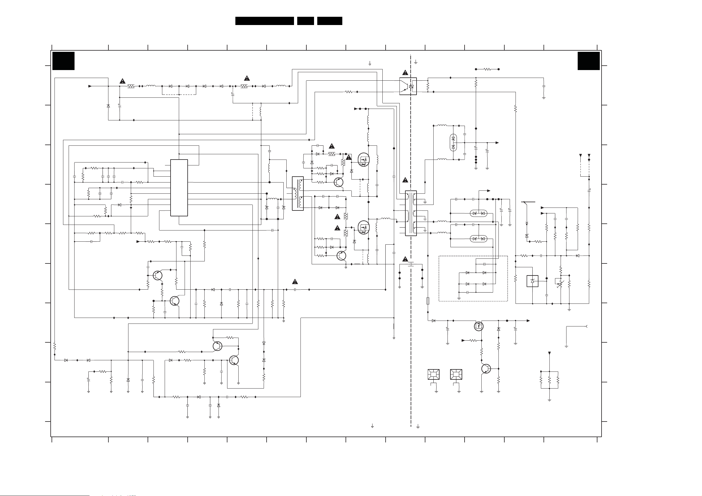
Circuit Diagrams and PWB Layouts
69Q528.1A LA 7.
Display Supply (32”): Part 2
1 23456789
A2 A2
DISPLAY SUPPLY: PART2
HOT GROUND
BIAS SUPPLY
5005
2000V
1n5
80R
2000V
1n5
5040
4
3
TCET1102(G)
F029
1600V
15n
2017
8
7
6
5
3
80R
I114
2
1
15n
2011
1600V
F023
F300
I084
c001
A
25V_HOT
6081
B
VS-CONTROLLER
3002
39K
100K
3004
100p
2034
27K
2009
100p
100p
2035
2005
2040
560p
I103
3003
C
D
2K7
3048
3043
I104
10R
3009
3008
I021
3K3
330R
2007
E
470n
16V
F
2002
BZX384-C22
200p
2006
2004
I009
100p
630V
RES
6001
BAS316
3007
I028
1n0
10K
630V
470u
25V
I029
3000
4R7
I006
I007
I008
3006
I010
400V_HOT
I096
I048
I027
3005
33K
10K
3058
5M6
RES
I022
I025
5017
50R
3050
820K
SOFTSTART
CONTROL
I018
2027
3066
I047
CONTROL
MC34067P
I105
50V
15n
BC857BW
7017
10K
I023
3064
F007
3027
100K
2026
BAS316
7001
9
1
2
3
16
6
8
7
11
3053
680K
10K
RES
6082
9009
I020
50V
2n2
EN|UA
OSCC
OSCR
OSCCC
OS
EAO
Ip
In
SOST
3012
I097
15
4
6080
BYG22D
VCC
VREF
OA
OB
PGND
FI
GND
2050
15K
7018
BC847BW
I044
6079
BYG22D
RES9008
5
14
12
13
10
I012
3065
68K
1n0
3061
CURRENT
PROTECTION
I024
16V
2008
3013
470n
I095
100K
6011
BAS316
10K
6077
BYG22D
I033
6010
2003
2015
10n
BAS316
I099
80R
5016
80R
BAT54 COL
2016
100n16V
470p
2064
470p
5010
1m0
I108
F009
6004
4
2
I100
I101
I107
3
BAT54 COL
5001
S13932-04
2060
I043
3100
10R
F299
400V_HOT
F018
80R
5007
I001
I064
2061
2n2
I003
6007
BAS316
2n2
6003
3035
BAS316
I045
3016
3K3
6
3029
3K3
7
I039
9
6008
10
BAS316
3028
3K3
3020
3K3
3019
3K3
3K3
2062
2n2
I042
6027
BAS316
I109
I052
6028
BAS316
I145
100R
3014
2072
1n0
2065
2n2
6002
BAS316
2071
1n0
HIGH SIDE
DRIVE
I038
F002
STP15NK50ZFP
1
47R
3015
I046
6013
I037
BC857BW
7007
I004
LOW SIDE
DRIVE
100R
3017
STP15NK50ZFP
I057
47R
3018
6012
I059
I051
BC857BW
7008
I055
BZG05C15
I294
9024
7006
1
BZG05C15
9025
c002
7005
80R
5008
I002
2
80R
3
I111
2013
50R
5004
I110
F005
2
5013
3
I113
I112
2012
50R
5041
3033
I098
I049
1R0
1m0
6078
I053
I050
BYG22D
80R
9004
5009
2063
5015
F003
F004
6005
F008
I106
GND3
I036
50V
RES2018
15R
100n
3001
100R
3045
3046
I034
15R
15R
3021
2014
I081
2n2
2000V
G
I139
6020
OVERVOLTAGE
PROTECTION
6009
I142
PDZ18-B
I141
2010
100u
470R
3010
3011
470R
6022
2019
BZX384-C4V7
BAS316
6051
3056
220R
3068
2K2
I136
I135
47R
10n
3047
431I
3067
100R
I143
BAS316
H
I
3070
1K0
2046
BC857BW
7009
I137
10K
3071
6006
3
31I
BAS316
47n
2048
3075
1K0
I140
I138
2077
I132
1n0
6017
2n2
2047
10n
BAS316
I011
7004
BC847BW
3055
470R
6015
BAS316
I296
6014
BZX384-C22
I295
10K
3089
I131
HOT GROUND
7002
5002
BS51
2000
470p
COLD GROUND
1
2
I117
9
10
11
GND_COLD
12
13
14
GND_COLD
15
16
GND_COLD
F033
F032
1005
COLD GROUND
3101 313 6154.4
1 23456789101112
10 11 12 13
2K2
3069
I063
I116
I073
I076
I154
3.15A T
I155
6016
BYW29EX-200
1009
HEATSINK
GND_COLD
F021
I062
5027
5028
5025
5026
50R
50R
50R
50R
I070
3
6044
STPS20L45CT
1
I072
2029
50V
1n0
I074
2045
1n0
50V
I077
2025
2
2028
I056
3
I054
3
50V
1n0
2020
50V
1n0
GND_COLD
2001
1n0
6021
STPS20H100CT
2049
50V
1n0
6025
STPS20H100CT
ONLY 295V VERSION
6033
BYV27-600
6031
BYV27-600
2067
100p
2033
GND_COLD
HEATSINK
I156
25V2m2
+24V
1004
GND_COLD
STP16NF06FP
7012
2
3031
22K
BC847BW
3057
F016
F028
F017
F027
50V
BYV27-600
BYV27-600
7014
GND_COLD
3999
1K0
220R
2m2 25V
2021
GND_COLD
F012
2
2
2066
100p
6034
6032
3
1
I158
4K7
3032
I161
F022
2m2 25V
+24V
F025
F024
1
I151
1
6018
GND_COLD
+12Vd
35V1m8
2022
GND_COLD
PDZ15-B
I159
1K0
3044
I160
5K6
3036
3022
35V1m8
2039
I085
3030
F006
2052
GND_COLD
680R
18K
25V220u
3023
15K
7010
TS2431
ON-OFF
BAT54 COL
I082
+12Vd
6083
I089
1
3
+15V
+24V
3081
56K
K
A
2023
GND_COLD
3052
2024
220n
16V
R
2
2030
I153
1K2
3080
GND_COLD
470n
3082
F014
33K
16V
100n
I094
+24V
2031
3037
3026
Vs
Voltage
Adj.
1K2
10n
I119
15K
3025
GND_COLD
3083
RES
2032
I121
RES
3038
1%
1K8
I093
470R
3034
GND_COLD
1K2
13
+12Vd
+24V
F030
9060
9061
I152
2041
I088
22n
15KMRS25 1%
3024
3040
8K2
I092
6023
BAS316
2K2
3041
1%
1002
GND screw
H_16800_002.eps
170407
1002 G13
3064 F3
F299 B8
3065 E4
3066 F2
3067 H1
3068 H3
3069 A10
3070 H4
3071 H4
3075 G5
3080 H12
3081 E12
3082 H13
3083 H13
3089 H5
3100 A8
3999 A11
5001 C6
5002 D9
5004 D8
5005 C8
5007 B8
5008 B8
5009 B5
5010 A6
5013 E8
5015 C6
5016 D6
5017 A3
5025 D10
5026 E10
5027 B10
5028 C10
5040 D8
5041 E8
6001 D2
6002 D7
6003 C7
6004 D6
6005 D5
6006 I4
6007 C7
6008 D7
6009 H1
6010 G4
6011 F4
6012 E8
6013 C8
6014 H5
6015 H5
6016 G10
6017 I4
6018 G11
6020 H1
6021 D11
6022 H2
6023 E13
6025 E11
6027 C7
6028 E7
6031 F11
6032 F11
6033 F11
6034 F11
6044 B10
6051 H3
6077 A4
6078 A5
6079 A4
6080 A3
6081 B1
6082 A3
6083 E12
7001 C3
7002 A9
7004 H5
7005 C8
7006 D8
7007 C7
7008 E8
7009 H4
7010 F12
7012 G11
7014 H11
7017 F3
7018 F3
9004 B5
9008 A3
9009 A3
9024 D8
9025 E8
9060 C13
9061 C13
F002 C8
F003 D6
F004 D6
F005 D8
F006 G12
F007 F3
F008 D5
F009 D6
F012 D11
F014 F13
F016 B11
F017 C11
F018 B8
F021 A11
F022 A11
F023 F9
F024 D11
F025 D11
F027 C11
F028 C11
F029 C9
F030 C13
F032 F9
F033 F9
F300 F9
I001 B8
I002 C8
I003 C7
I004 D7
I006 B2
I007 C2
I008 C2
I009 D2
I010 D2
I011 I5
I012 E4
I018 E3
I020 F3
I021 E1
I022 F2
I023 F3
I024 F4
I025 F2
I027 C2
I028 G2
I029 G2
I033 F4
I034 F6
I036 F5
I037 C8
I038 C7
I039 D7
I042 C7
I043 A8
I044 A4
I045 C7
I046 C7
I047 A3
I048 A2
I049 A5
I050 A5
I051 E7
I052 D7
I053 A5
I054 E10
I055 E8
I056 D10
I057 E8
I059 E8
I062 A10
I063 A10
I064 B7
I070 B10
I072 C10
I073 D10
I074 D10
I076 E10
I077 E10
I081 F7
I082 E12
I084 F9
I085 E12
I088 D13
I089 E12
I092 E13
I093 F13
I094 F13
I095 A4
I096 A2
I097 A3
I098 A5
I099 A6
I100 A6
I101 A6
I103 C1
I104 D2
I105 E3
I106 E5
I107 C6
I108 D6
I109 C7
I110 D8
I111 C8
I112 E8
I113 E8
I114 E9
I116 B10
I117 C9
I119 E13
I121 E13
I131 I5
I132 I4
I133 I3
I134 I3
I135 H2
I136 H3
I137 H4
I138 H4
I139 G4
I140 H5
I141 H1
I142 H1
I143 H1
I145 E7
I151 D11
I152 C13
I153 H12
I154 E10
I155 G10
I156 G10
I158 G11
I159 G11
I160 H11
I161 H11
I294 C8
I295 H6
I296 H6
c001 G9
c002 F8
1004 H10
1005 F9
1009 H10
2000 E9
2001 D11
2002 B2
2003 A5
2004 C2
2005 D1
2006 C2
2007 E1
A
2008 G4
2009 D1
2010 H1
2011 E9
2012 E8
2013 D8
2014 F6
2015 F5
2016 E6
2017 C9
2018 G5
B
2019 H2
2020 C11
2021 C11
2022 D11
2023 A12
2024 E12
2025 B10
2026 G3
2027 F2
2028 C10
2029 D10
2030 F13
C
2031 D13
2032 D13
2033 G10
2034 C1
2035 C1
D
E
F
G
H
I
2039 D12
2040 C1
2041 D13
2045 E10
2046 I3
2047 I4
2048 I4
2049 E11
2050 E3
2052 G12
2060 C6
2061 B7
2062 D7
2063 C6
2064 D6
2065 D7
2066 E11
2067 F11
2071 E7
2072 C7
2077 H4
3000 A2
3001 G5
3002 C1
3003 C1
3004 D1
3005 C2
3006 D2
3007 E2
3008 E2
3009 E1
3010 H1
3011 H2
3012 F3
3013 G4
3014 C7
3015 C7
3016 C7
3017 D7
3018 E7
3019 E7
3020 E7
3021 G6
3022 B12
3023 E12
3024 E13
3025 F13
3026 F13
3027 G3
3028 E7
3029 C7
3030 F12
3031 G11
3032 H11
3033 A5
3034 F13
3035 C7
3036 H11
3037 E13
3038 E13
3040 E13
3041 F13
3043 D1
3044 H11
3045 G5
3046 G6
3047 H3
3048 D1
3050 E3
3052 E13
3053 E3
3055 I5
3056 I3
3057 A11
3058 E2
3061 E4
50V
2u2
8K2
33K

Circuit Diagrams and PWB Layouts
Layout Display Supply Panel (32”) (Top Side)
1002 A7
1004 C11
1005 B10
1006 A1
1009 B10
1011 C3
1308 A1
1317 A10
1319 A10
1320 A10
1400 B1
1402 A1
1403 A2
1404 B2
1405 A2
1450 A4
1M09 C10
1M12 C11
1M90 C10
1P02 C3
1P11 C9
1P15 C10
1P22 C3
2000 A8
2002 A7
2003 A7
2004 A6
2005 A7
2010 A8
2011 B7
2012 C8
2013 C7
2014 A8
2017 A7
2020 C9
2021 C9
2022 A9
2033 B10
2039 A9
2041 A11
2052 B11
2066 B11
2067 B11
2400 C1
2401 B2
2403 B1
2404 B1
2406 A3
2407 A1
2408 B3
2410 A1
2411 A1
2803 B4
2804 B5
2806 B5
2809 C5
2810 C5
2811 A11
2815 A4
2816 A6
3000 A5
3014 B6
3015 C6
3017 C7
3018 C7
3024 A10
3026 A11
3033 A7
3050 A5
3053 A5
3058 A5
3080 A10
3082 A9
3083 A9
3400 C1
3401 A1
3402 A1
3403 A1
3404 A3
3405 A2
3450 B3
3451 A3
3800 A5
3805 C5
3807 B5
3810 A4
5001 B7
5002 B9
5004 C7
5005 C7
5007 B6
5008 C6
5009 B8
5010 B7
5013 C8
5015 A7
5016 A6
5017 A5
5025 B10
70Q528.1A LA 7.
5026 A10
5027 B9
5028 B9
5040 B7
5041 B7
5401 B3
5402 A2
5403 A3
5405 B2
5406 C10
5408 C10
5409 C3
5410 C2
5804 B5
6016 B10
6021 B10
6025 B11
6031 A11
6032 B11
6033 A11
6034 B10
6044 C9
6807 C3
6808 B5
6809 A5
7001 A7
7002 A8
7005 C6
7006 C8
7012 C11
7805 B5
7806 C5
9001 A3
9002 C11
9003 A2
9004 A8
9005 B3
9006 C10
9007 C11
9015 B2
9016 A7
9017 A6
9018 A11
9019 A7
9020 B8
9021 A7
9024 C7
9025 B8
9030 C9
9031 A10
9032 A10
9033 A9
9035 B9
9036 B10
9037 B9
9039 A10
9040 A10
9042 A1
9043 A9
9044 C11
9046 B1
9047 B5
9048 A11
9049 A11
9052 A11
9054 A11
9056 C9
9061 A10
9062 A1
9080 B8
9083 A11
9092 A8
9093 A7
9098 B4
9101 A4
9102 A8
9808 B5
9809 C4
9811 B5
9812 C5
9813 B5
9814 A5
3101 313 6154.4
H_16800_003.eps
170407
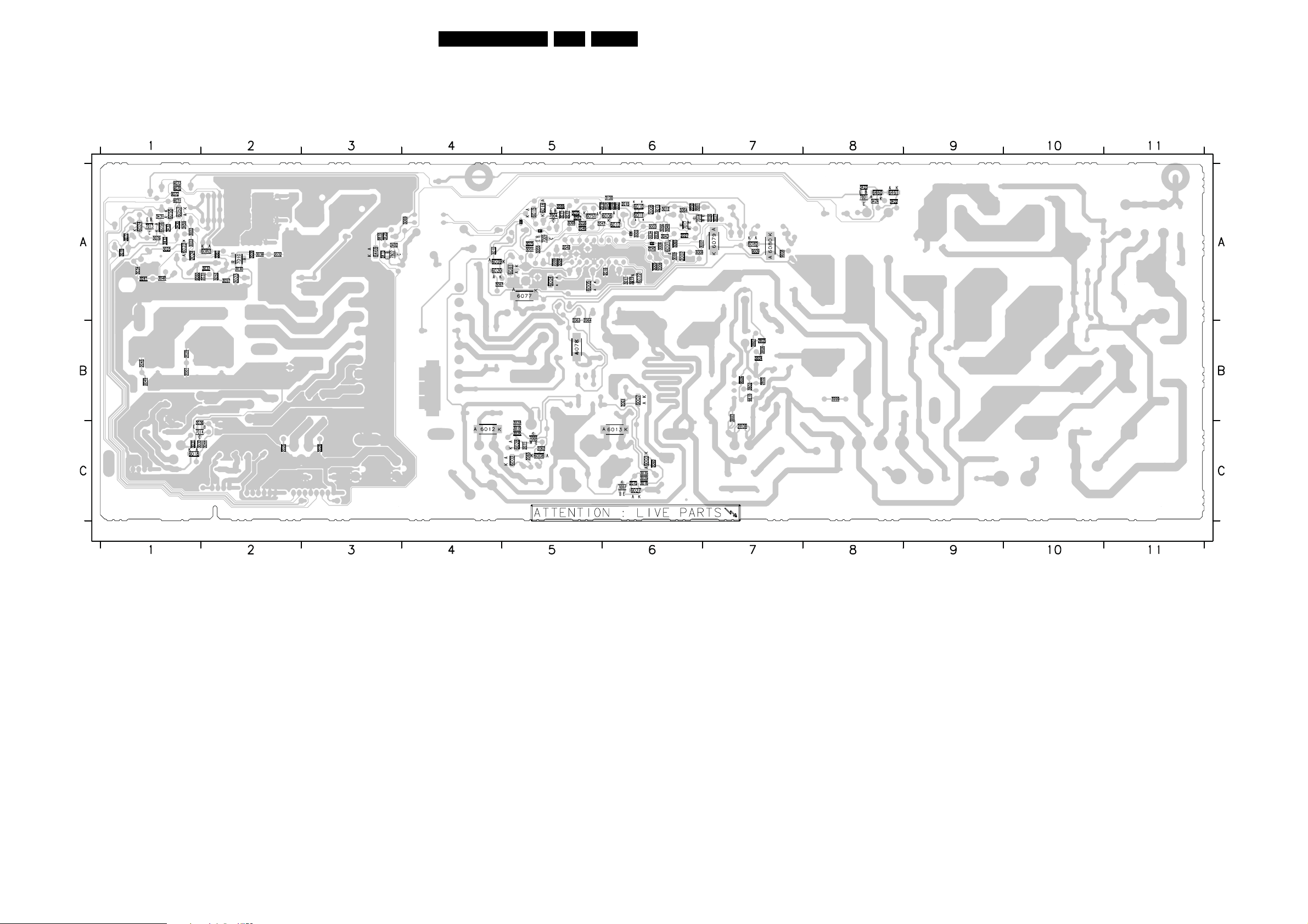
Circuit Diagrams and PWB Layouts
Layout Display Supply Panel (32”) (Bottom Side)
2001 B1
2006 A6
2007 A6
2008 A6
2009 A5
2015 A6
2016 A6
2018 A5
2019 A6
2023 A2
2024 A1
2025 C2
2026 A7
2027 A6
2028 C3
2029 B1
2030 A2
2031 A2
2032 A2
2034 A6
2035 A6
2040 A6
2045 B1
2046 A5
2047 A5
2048 A5
2049 B1
2050 A6
2060 C6
2061 B6
2062 C5
2063 A5
2064 A5
2065 C5
2071 C5
2072 C6
2077 A5
2402 A3
2802 B7
2805 B7
2807 B7
2808 C7
3001 A5
3002 A6
3003 A6
3004 A5
3005 A6
3006 A6
3007 A6
3008 A6
3009 A6
3010 A4
3011 A6
3012 A6
3013 A6
3016 C6
3019 C5
3020 C5
3021 A6
3022 A1
3023 A1
3025 A1
3027 A7
3028 C5
3029 C6
3030 A2
3031 C1
3032 C1
3034 A1
3035 C6
3036 C1
3037 A2
3038 A2
3040 A1
3041 A1
3043 A6
3044 C2
3045 A6
3046 A6
3047 A5
3048 A6
3052 A2
3055 A5
3056 A5
3057 A2
3061 A6
3064 A6
3065 A6
3066 A6
3067 A4
3068 A5
3069 A4
3070 A5
3071 A5
3075 A5
3076 A1
71Q528.1A LA 7.
3077 A1
3078 A1
3081 A2
3089 A5
3100 A6
3413 A3
3422 A8
3423 A8
3424 A8
3425 A3
3430 A1
3431 A1
3432 A1
3433 A1
3459 A1
3802 B7
3803 B7
3804 B7
3806 B7
3999 B8
6001 A6
6002 C5
6003 C6
6004 A5
6005 A5
6006 A6
6007 B6
6008 C5
6009 A4
6010 A6
6011 A6
6012 C4
6013 C6
6014 A5
6015 A5
6017 A6
6018 C1
6020 A4
6022 A6
6023 A1
6024 A1
6027 C6
6028 C5
6051 A5
6055 A1
6056 A1
6057 A1
6077 A5
6078 B5
6079 A7
6080 A7
6081 A5
6082 A7
6083 A2
6460 A8
6461 A8
6469 A3
7004 A5
7007 C6
7008 C5
7009 A5
7010 A2
7013 A1
7014 C1
7017 A6
7018 A6
7801 A8
7802 A3
9008 A7
9009 A7
9060 A1
9070 A1
9071 A1
9072 A1
9073 A1
9104 A6
9105 A5
9106 A5
9107 A6
9806 B7
9810 B7
9816 A3
3101 313 6154.4
H_16800_004.eps
170407

Circuit Diagrams and PWB Layouts
72Q528.1A LA 7.
Display Supply (42”): Mains Filter & Standby
3305 C4
1003 B4
1005 B4
1300 E3
1301 E4
1302 B4
1303 C4
1308 C1
1311 E6
1312 E7
1314 C2
1350 C9
1P02 B7
1P03 B7
1P22 B11
2300 C3
2301 C4
2302 C5
2304 D11
2305 F11
2307 D4
2309 E13
2310 C11
2311 C11
2313 F11
2314 E13
2315 C12
2316 D12
2317 C12
2318 D5
2319 B10
2320 D12
2321 C13
2323 C3
2324 C4
2325 C5
2327 B10
2330 E10
2331 F10
2332 H9
2333 G10
3300 C3
3301 C2
3302 D2
3303 E2
3304 B5
12345
A1 A1
MAINS FILTER + STANDBY
A
MAINS FILTER
B
120V for US
230V for EUR
4M7
F416
F419
1314
T5AH 250V(EUR/AP)
T6.3AH 250V(US)
4M7
3302
I419
4M7
3303
F413
F412
C
2
1
1308
F410
F411
3301
F415
F418
D
2300
470n
2323
I410
470n
3300
E
COLD GROUND
V_NOM
V_NOM
2
14
DMF3547HB60
V
2
5307
1
9315
1
1005
1302
500V
1003
1303
500V
5305
1300
I844
3
3
4
DMF2405H60
3305
220R
2324
F
3306 A14
3307 F10
3308 C14
3309 E10
I821
I846
470n
I416
2307
1301
1
GND screw
2301
220p
3310 B13
3311 F11
3312 E11
3313 F10
3314 F13
2
14
470n
9309
I411
5306
DMF3547HB60
9303
I299
3316 D6
3317 D5
3318 C10
3319 D6
3320 D7
3304
220R
3
2318
2302
I297
470p
9317
9316
470n
3321 E10
3322 E12
3323 E12
3324 E12
3325 G8
2325
3317
1R0
3326 H9
3327 G9
3328 G9
3329 G9
3330 B12
5303 D6
5304 F13
5305 C4
5307 D3
5308 D12
6304 B10
6307 C11
6308 E10
6309 E10
6314 C14
6315 A12
6316 A13
6317 B13
6318 B13
6354 C14
6355 B13
6360 E9
6361 E9
7305 E11
7306 E13
7307 B14
7308 G9
7309 G10
9301 D14
9302 C12
9303 D5
9304 E10
9308 D12
9309 C5
9310 E11
9311 B13
9312 F135306 C5
9315 E3
9316 D5
9317 D5
9318 D76305 B11
9319 D7
F410 C1
F411 C1
F412 C2
F413 C2
F415 D2
F416 D2
F418 D2
F419 D2
F422 F9
F423 F8
F430 C7
F431 D8
F432 G8
F524 C14
I297 D5 I419 D2
I299 E5
I410 C3
I411 C5
I416 D4
I424 E9
6 7 8 9 10 11 12
25V_HOT
6304
BAS316
1N5062
1N5062
I816
22K
3309
3321
3313
I820
2327
I842
I836
1u0
2319
470n
I861
1M0
2K7
9304
I860
18K
I835
3318
470R
AVS1ACP08
2330
2331
BAS316
4
TS6B
56n
2310
9310
7305
MODE
8
VM
2
OSIN
47n
I841
47n
100p
2305
6305
VDD
VSS
6307
4
OSOUT
1
1P22
1
2
23
2311
1
2304
67
NC
5
VG
I839
3
3311
100K
2313
50V
47u
470n
3319
DTH40383H65
1
1R0
2
HEATSINK
5303
1311
GND4
1P03
1
2
B2P-VA-BF-BK
1P02
1
2
B2P-VA-BF-BK
F430
F431
4
1R0
1R0
3320
9318
1312
9319
COLD GROUND
F423
3316
3
I827
HEATSINK
1350
3
4
G5PA-1-5VDC
I424
RELAY +
6361
6360
BAS316
BAS316
2
1
6309
I814
6308
I815
RELAY -
F422
3307
I814 E10
I815 F10
I816 E10
I817 D11
I820 F10
I821 B4
I822 E12
I823 E12
I824 E12
I825 E13
I826 F13
I827 D7
I828 B13
I829 A14
I830 A13
I831 C13
I832 C12
I833 B13
I834 C13
I835 B10
I836 B10
I837 E13
I838 E13
I839 E11
I840 E11
I841 F11 I861 D10
I842 F10
I844 C4
I846 C4
I860 F10
13 14
7307
I833
9311
BZX384-C33
I834
I825
56n
4R7
25V_HOT
TCET1102(G)
3308
22K
3306
1K0
I829
I864
6354
9301
2315
I862
80R
330u
I830
6316
BZX384-C33
I828
6355
BYG10
47K
3310
6318
BAS316
6317
330u
2321
330u
I831
I832
7306
I837
2314
AVS10CB
5304
100u
9312
2309
I826
3314
47n
I838
400V_HOT
2M2
2316
I823
2317
9308
3323
100R
6315
BZG03-C200
272V(30V)
10n
9302
5308
330u
2320
I824
3324
100R
400V_HOT
399V_HOT
3330
56n
400V_HOT
56n
I817
3312
I822
100R
3322
I840
100R
I862 D12
I864 B14
I865 G9
I866 G9
F524
6314
BYG10
LATCH
A2
BZG03-C200
I870 G9
A
B
C
D
E
F
G
H
3101 313 6171.4
123456
+5V2
A2
Standby
F432
3325
10K
I866
15K
2332
3326
78
3327
6K8
I865
3K9
3328
3329
2333
220R
I870
7308
BC847BW
2n2
7309
BC817-25W
2n2
G
H
H_16800_005.eps
180407
9
10 11
12 13 14

Circuit Diagrams and PWB Layouts
73Q528.1A LA 7.
Display Supply (42”): Supply
1 2345678
A2 A2
SUPPLY
9009 9003
3000
A
25V_HOT
6025
BYG22D
BC847BW
7013
B
I849
VS-CONTROLLER
I011
2040
3009
560p
3K3
2007
470n
3003
3004
16V
100K
3059
5K6
27K
3043
10R
I009
2062
3048
3008
I021
330R
C
D
E
I096
5017
50R
4R7
I047
1K0
3092
3093
3002
15K
3098
56K
100p
2K7
2061
100p
2058
100p
1n0
I010
6038
I847
3058
3007
5M6
10K
400V_HOT
I025
3044
10K
F
I028
I029
G
3010
I141
470R
H
2010
100u
3011
470R
6022
2019
BZX384-C4V7
I
I097
6032
BYG22D
BC857BW
7014
2K2
I049
I027
2006
25V
I008
10K
3006
BAS316
3050
1M5
SOFTSTART
CONTROL
I018
50V
15n
2027
I022
F007
3027
100K
3047
47R
10n
I005
3005
33K
I023
3051
2026
I134
BC857BW
7011
10K
50V
2n2
6026
BAT54 COL
6033
BYG22D
I048
2K2
I020
I135
3094
3012
3056
220R
I006
1m0
2003
CONTROL
3049
100K
PROTECTION
10K
7012
BC847BW
3042
I137
2K2
I136
A1
I133
2046
BIAS SUPPLY
1116
3.0A T
1114
T3.0A
I098
I007
9
1
2
3
16
6
8
7
11
I012
CURRENT
I024
6011
BAS316
16V
10K
2008
470n
3013
6029
PDZ18-B
3039
1K0
10K
3060
LATCH
6006
BAS316
47n
2048
6024
BYG22D
2050
I139
I138
3036
1n0
7001
EN|UA
OSCC
OSCR
OSCCC
OS
MC34067P
EAO
Ip
In
SOST
I033
6010
10K
2037
I132
6017
I099
I101
1n0
3054
BAS316
7009
BC857BW
BAS316
15
VCC
GND
4
2047
10n
5010
80R
VREF
OA
OB
PGND
FI
BAS316
470K
3028
1K0
47n
I100
9008
680u
2002
5
14
12
13
10
I295
6020
9017
F425
PDZ18-B
6018
3035
100R
I296
I036
2015
50V
10n
22n
2063
I140
7004
BC847BW
I850
3055
I131
220R
HOT GROUND
5009
3001
80R
F030
F008
100R
3045
BAT54 COL
6005
2016
100n 16V
100R
I040
I041
3046
F003
5016
80R
I108
2053
I034
100R
3021
6015
6014
3089
HOT
2054
80R
5015
4
2
470p
6004
F009
100R
BAS316
BZX384-C33
10K
470p
I107
3
BAT54 COL
2014
470p
2000V
I851
2057
5001
S13932-04
+5V2
COLD
400V_HOT
2055
2n2
I042
BAS316
I109
I052
6028
BAS316
I145
6027
3014
100R
2036
1n0
2035
1n0
I055
2052
2n2
6002
BAS316
I014
HIGH SIDE
DRIVE
I038
3015
I046
I037
BC857BW
7007
I855
3017
3018
I059
I051
3065
1K0
2056
2n2
6007
BAS316
2n2
6003
3062
BAS316
3K3
3016
I045
3K3
6
3029
3K3
7
I039
9
6008
10
BAS316
3061
3K3
3020
3K3
3019
3K3
I081
F018
F002
7005
47R
STP15NK50ZFP
6013
BZG05C15
I294
LOW SIDE
DRIVE
7006
100R
STP15NK50ZFP
I057
47R
6012
BZG05C15
BC857BW
7008
c002
GND3
9013
F299
I064
9001
5007
5008
5004
I112
5027
80R
I013
80R
I852
I111
2013
50R
F005
FLM 1/6W
5013
I113
2012
50R
5005
I110
399V_HOT
50R
9014
2000V
1n5
9011
5012
80R
80R
9012
2000V
1n5
2011
c003
c001
F029
2060
2017
1600V
22n
22n
15n2080
2059 15n
I114
1600V
15n
GND4
2001
6076
BZX384-C3V3
7015
BC857BW
1K0
1K5
2071
F034
F035
F036
F037
100n
F145
2072
F032
F031
Power-Good
4u7
F033
1M90
1
2
3
4
5
6
B6B-PH-K
+12V
F045
6045
5030
80R
BYG22D
2075
+12V
F142
I019
3095
4K7
3096
3097
COLD GROUND
3101 313 6171.4
234
9101112 13
400V_HOT
I084
10u 50V
+24VB
4
7002
3
TCET1102(G)
400V_HOT
I845
470p
+30V
B8B-PH-K-S
2000
470p
5011
BS51
5002
1M09
1
2
3
4
B4B-PH-K
1P11
1
2
3
4
5
6
7
8
9031
4K7
4K7
4K7
3082
3080
3081
3083
I062
1
I063
2
6070
STPS8H100FP
50V
5021
80R
5022
80R
1P15
B3B-PH-K
Boost
Standby
9033
2028
1n0
6074
STPS8H100FP
6075
STPS8H100FP
I072
BYV28-600
2029
50V
1n0
6021
STPS8H100FP
2045
1n0
2021
100p
6072
BYV28-600
6073
BYV28-600
I074
STPS8H100FP
I077
+12V
1
2
3
DIM-control
Boost
Light_on_off
A1
GND screw
50V
2044
F027
F017
6071
2070
100p
2034
1n0
50V
6041
2039
50V
1n0
2022
2042
50V
1n0
6031
STPS8H100FP
6040
2049
1n0
1310
1
2
I856
1
1322
1n0
50V
2020
35V1m8
50V
50V
OR +295V
I857
35V
1m8
F028
2038
2009
1n0
2018
1n0
+24VA
5003
I116
80R
I070
9016
I117
5006
80R
I001
9015
BYV28-600
I002
5025
80R
9029
I004
5026
9030
I003
80R
I015
I016
I017
I073
I076
I032
1115
I031
T3.0A
1M12
I868
1
5028 3u3
2
3
5029
I869
+12V
OR +295V
F046
B4B-PH-K
+24VA
4
10
B10B-EH-A
3u3
1P10
+5V2
DIM-control
Power-Good
Light_on_off
1
2
3
4
5
6
7
8
9
4K7
3084
OR +12V
35V1m8
2066
+24VA
OR +295V
35V
1m8
9019
9020
9021
9022
4K7
4K7
3087
3088
3022
680R
+18V
I085
2064
3n3
K
A
31
18K
3030
1109
HEATSINK
1m835V
2041
F075
+3V3
9024
9023
I858
I859
9026
9027
2043
9028
R
+24VB
9025
4K7
3023
I094
I867
+24VA
OR +295V
F021
F140
3068
220R
2023
470n
3057
220R
F016
2031
10K
15K
3063
3052
3037
F012
3024
I089
2024
10K
I030
7010
2
1m8 35V
F040
F041
F042
F043
F044
TS2431
2030
3091
1R0
F014
50V
15n
1113
HEATSINK
+24VB
B12P-PH-K
100n
3025
MRS25 1%
3026
+12V
1316
F146
15K
1
2
3
4
5
6
7
8
9
10
11
12
10n
I853
15K
BAS316
1K8
470R
HEATSINK
B12P-PH-K
2033
6023
I093
3034
1110
1317
OR +12V
OR +12V
F024
1u0
I088
I092
1K0
3069
1K5
1
2
3
4
5
6
7
8
9
10
11
12
+18V
+18V
2025
3040
3041
F025
16V
2032
1u0
8K2
3038
7016
BC857BW
3071
100R
33K
9002
6069
BZX384-C3V3
1319
B14B-PH-K
F022
3999
1K0
F147
3n3
I121
4K7
6044
F141
2069
1
2
3
4
5
6
7
8
9
10
11
12
13
14
H_16800_006.eps
3
1211101987651
2076
9032
+12V
3070
BAS316
100n
1321
B14B-PH-K
OR +295V
33n
1K0
6042
6043
3072
+3V3
1
2
3
4
5
6
7
8
9
10
11
12
13
14
180407
+24VA
F023
PDZ3.3-B
I090
PDZ10-B
I091
100R
2081
100n
A
B
C
D
E
F
G
H
I
1109 F12
1110 F13
1113 F12
1114 A3
1115 H9
1116 A3
1310 H11
1316 H12
1317 H13
1319 H13
1321 H13
1322 I11
1M09 H9
1M12 H10
1M90 I8
1P10 H10
1P11 H9
1P15 H10
2000 A9
2001 G8
2002 B4
2003 A3
2006 C2
2007 E1
2008 G3
2009 G11
2010 H1
2011 E8
2012 E8
2013 D8
2014 F6
2015 F4
2016 D5
2017 C8
2018 G11
2019 H2
2020 D11
2021 F10
2022 F11
2023 B12
2024 D12
2025 D13
2026 G2
2027 F2
2028 C11
2029 E10
2030 E12
2031 C12
2032 D13
2033 D12
2034 E11
2035 E7
2036 C7
2037 H4
2038 F11
2039 E11
2040 C1
2041 G11
2042 G11
2043 G12
2044 D11
2045 E10
2046 I3
2047 I4
2048 I4
2049 G11
2050 F4
2052 D7
2053 D5
2054 C5
2055 D7
2056 B6
2057 C6
2058 C2
2059 D8
2060 F8
2061 C2
2062 D1
2063 G5
2064 D12
2066 D11
2069 G13
2070 E11
2071 I7
2072 I7
2075 I8
2076 D13
2080 C8
2081 D13
3000 A1
3001 F5
3002 C1
3003 C1
3004 D1
3005 C2
3006 D2
3007 E1
3008 E1
3009 E1
3010 H1
3011 H1
3012 F3
3013 G3
3014 C7
3015 C7
3016 C6
3017 D7
3018 E7
3019 E6
3020 E6
3021 G5
3022 C11
3023 D12
3024 D12
3025 E12
3026 E12
3027 G2
3028 G4
3029 C6
3030 E11
3034 E12
3035 E5
3036 H4
3037 C12
3038 D13
3039 H3
3040 D13
3041 E13
3042 G3
3043 D1
3044 F2
3045 G5
3046 F5
3047 H2
3048 D1
3049 E3
3050 E2
3051 F2
3052 C12
3054 F4
3055 I5
3056 I3
3057 B12
3058 E2
3059 C1
3060 H3
3061 E6
3062 C6
3063 C12
3065 B6
3068 B12
3069 G13
3070 D13
3071 E13
3072 F13
3080 A10
3081 A10
3082 A11
3083 A11
3084 A11
3087 A11
3088 A12
3089 H5
3091 D12
3092 B1
3093 B2
3094 B3
3095 H6
3096 H7
3097 I7
3098 C1
3999 A13
5001 C6
5002 F9
5003 C10
5004 D8
5005 C8
5006 D10
5007 B8
5008 B8
5009 B5
5010 A4
5011 D9
5012 D8
5013 E8
5015 C5
5016 D5
5017 A2
5021 G10
5022 G10
5025 E10
5026 E10
5027 E8
5028 H10
5029 H10
5030 H8
6002 D7
6003 C6
6004 D5
6005 D5
6006 I3
6007 C6
6008 D6
6010 G4
6011 F4
6012 E7
6013 C7
6014 H5
6015 G5
6017 I4
6018 E4
6020 E4
6021 E10
6022 H1
6023 E13
6024 A4
6025 A1
6026 H3
6027 C7
6028 E7
6029 G3
6031 G11
6032 A2
6033 A3
6038 D2
6040 G11
6041 E11
6042 E13
6043 F13
6044 E13
6045 H8
6069 G13
6070 D10
6071 D11
6072 F10
6073 F10
6074 D10
6075 D10
6076 H7
7001 C4
7002 B9
7004 H4
7005 C8
7006 D8
7007 C7
7008 E7
7009 G4
7010 E12
7011 F2
7012 F3
7013 B1
7014 B2
7015 H7
7016 E13
9001 E8
9002 F13
9003 A3
9008 B5
9009 A2
9011 D8
9012 E8
9013 D8
9014 C8
9015 D10
9016 D10
9017 E4
9019 I11
9020 I11
9021 I11
9022 I11
9023 H11
9024 H11
9025 H12
9026 I11
9027 I11
9028 I12
9029 E9
9030 F9
9031 I9
9032 D13
9033 I10
F002 C7
F003 C5
F005 D8
F007 F2
F008 D5
F009 D6
F012 C12
F014 E12
F016 C12
F017 D11
F018 A7
F021 A13
F022 A13
F023 E13
F024 C13
F025 C13
F027 D11
F028 D11
F029 A8
F030 D5
F031 H8
F032 H8
F033 H8
F034 I7
F035 I7
F036 I7
F037 I7
F040 H12
F041 H12
F042 I12
F043 I12
F044 I12
F045 H8
F046 I9
F075 G11
F140 B12
F141 G13
F142 H6
F145 H7
F146 C12
F147 C13
F299 A8
F425 E5
I001 D9
I002 E10
I003 F10
I004 E10
I005 A2
I006 A3
I007 C3
I008 D2
I009 C1
I010 D2
I011 C1
I012 E4
I013 B8
I014 B7
I015 F10
I016 F10
I017 G10
I018 E2
I019 H7
I020 F3
I021 E1
I022 F2
I023 F2
I024 F3
I025 F1
I027 C2
I028 G1
I029 G2
I030 D12
I031 H9
I032 H10
I033 F4
I034 F5
I036 F5
I037 C7
I038 C7
I039 D6
I040 H5
I041 H5
I042 C7
I045 C6
I046 C7
I047 B2
I048 B3
I049 B2
I051 E7
I052 D7
I055 E7
I057 E7
I059 E7
I062 B10
I063 B10
I064 B8
I070 D10
I072 D10
I073 G10
I074 G10
I076 G10
I077 G10
I081 F6
I084 F9
I085 D12
I088 D13
I089 D12
I090 E13
I091 F13
I092 E13
I093 E13
I094 F12
I096 A2
I097 A2
I098 A4
I099 A4
I100 A5
I101 A4
I107 C6
I108 D5
I109 D7
I110 D8
I111 C8
I112 E8
I113 E8
I114 D8
I116 C10
I117 D10
I121 D13
I131 I5
I132 I4
I133 I3
I134 H2
I135 G3
I136 H3
I137 G3
I138 H4
I139 G4
I140 G5
I141 H1
I145 E7
I294 C8
I295 E5
I296 E4
I845 D9
I847 D1
I849 C1
I850 I4
I851 C6
I852 B8
I853 C12
I855 D7
I856 I11
I857 I11
I858 I11
I859 I11
I867 I12
I868 H9
I869 H9
c001 F8
c002 F7
c003 F8

Circuit Diagrams and PWB Layouts
74Q528.1A LA 7.
Display Supply (42”): DC - DC
123456
7891011
DC-DC
A3 A3
A
B
+18V
OR +12V
C
D
E
F
3101 313 6171.4
3407
0R1
3408
0R1
3419
0R1
10K
BZX384-C15
10K
3422
I618
3423
7406
BC847BW
3421
I617
6404
I620
3424
12345
1K5
1K5
I600
9401
9402
7402
STP55NF06FP
2
1
I619
1
470p
470p
3406
3401
2403
3
1K5
10K
I606
100n
I601
3
6403
I614
BAS316
I622
6402
BZX384-C18
6401
5402
STPS745FP
50R
9405
2409
6405
BAS316
2411
9406
BC15605-00
+12V
4
3403
1K0
2402
82K
3404
1m8 35V
3405
2404
2401
10K
100n
35V1m8
47R
3418
2410
3430
+12V
OR +12V
68n
I621
220R
+18V
I613
I624
2407
8 DCOL
7IS
10n
6
5 CIN_NEG
VCC
MC34063AD
IPK
OSC
7401
SRQ
REFERENCE
REGULATOR
2408
4u7
SWC
SWE
GND
HEATSINK
1400
+30V
3409
1
I607
10K
I610
2
2405
3TIMC
I612
220p
4
3410
3411
1K0
I623
7407
BC857BW
1K0
2406
I602
220p
3427
3412
678
I611
15K
470R
3425
470R
BC807-25W
7403
I615
+18V
3402
100K
3426
15K
10K
3413
I609
7404
BC847BW
9403
3414
22R
3420
6406
BAS316
OR +12V
I616
7405
BC817-25W
9404
I603
6407
BAS316
3415
22R
47R
BAS316
6409
I604
I608
3416
100R
3417
9407
100R
91011
2
5401
H_16800_007.eps
180407
A
B
C
D
E
F
1400 E7
2401 B4
2402 B4
2403 D3
2404 E4
2405 C7
2406 B8
2407 C5
2408 D6
2409 D3
2410 D4
2411 B3
3401 C3
3402 E8
3403 D4
3404 E4
3405 D4
3406 B3
3407 B2
3408 B2
3409 C7
3410 B7
3411 C8
3412 D8
3413 C8
3414 B10
3415 B9
3416 C10
3417 C10
3418 C5
3419 B2
3420 B10
3421 C1
3422 C2
3423 D2
3424 E1
3425 B8
3426 B9
3427 C8
3430 D4
5401 B4
5402 C3
6401 B3
6402 C3
6403 B3
6404 D1
6405 D3
6406 B9
6407 C9
6409 C10
7401 C6
7402 B2
7403 B8
7404 C9
7405 C9
7406 D2
7407 B8
9401 A2
9402 A2
9403 D9
9404 D9
9405 C3
9406 C3
9407 C10
I600 B2
I601 B3
I602 B8
I603 B9
I604 B10
I606 C4
I607 C7
I608 C10
I609 C9
I610 C7
I611 C8
I612 D7
I613 D5
I614 B3
I615 C8
I616 C9
I617 D1
I618 D2
I619 D2
I620 D1
I621 D5
I622 B3
I623 E7
I624 C5

Circuit Diagrams and PWB Layouts
Layout Display Supply (42”) (Top Side)
1003 E2
1005 E2
1109 A10
1110 D9
1113 C10
1300 C7
1301 C1
1302 E2
1303 E2
1308 E1
1310 D10
1311 E4
1312 D3
1314 F2
1316 D10
1317 D10
1319 D10
1321 D10
1322 C10
1350 A6
1400 E9
1M09 E10
1M12 F10
1M90 F9
1P02 A4
1P03 F3
1P10 A9
1P11 F8
1P15 F10
1P22 A5
2000 B7
2001 E7
2002 D5
2003 F7
2010 D6
2011 A5
2012 F6
2013 F5
2014 C6
2017 A5
2020 F8
2021 A10
2022 A9
2032 B10
2038 B10
2041 C9
2043 B8
2059 A5
2060 B5
2066 C9
2070 A9
2075 E9
2080 A6
2300 E2
2301 D2
2302 B2
2304 C3
2307 D1
2309 C5
2310 C4
2311 D3
2313 C6
2314 C5
2315 A2
2316 A3
2317 B3
2318 B1
2319 D4
2320 B5
2321 B3
2323 E2
2324 D2
2325 B2
2327 E4
2401 F10
2402 E10
3000 E7
3014 F4
3015 F4
3017 F5
3018 F5
3024 B10
3026 B9
3038 B10
3050 D6
3058 E6
3080 A10
3081 A10
3082 A10
3083 A10
3084 A10
3087 A10
3088 A10
3300 F2
3301 E1
3302 E1
3303 D1
3304 D2
3305 E2
3307 C5
3308 F3
3309 B5
3314 C5
3316 A1
3317 B1
3318 D3
3319 B2
3320 A1
3330 A5
3420 E8
5001 E4
5002 D8
5003 D8
5004 E5
5005 F4
5006 D8
5007 F5
5008 F5
5009 E6
5010 E7
75Q528.1A LA 7.
5011 A7
5012 F5
5013 F6
5015 D5
5016 D5
5017 E7
5021 C8
5022 C9
5025 A8
5026 A8
5027 E6
5028 F10
5029 E10
5030 E8
5303 A1
5304 C5
5305 E1
5306 C2
5307 D1
5308 B4
5401 E9
5402 E9
6021 A9
6031 C9
6040 C10
6041 A10
6070 A8
6071 A9
6072 A9
6073 B9
6074 D9
6075 D9
6307 D4
6308 B5
6309 B5
6401 F9
7001 E5
7002 C7
7005 F4
7006 F6
7305 B5
7306 D5
7307 F4
7402 F8
9001 F6
9008 D6
9011 F6
9012 F6
9013 F5
9014 F4
9015 D8
9016 D8
9029 B8
9030 B8
9031 D10
9033 C10
9301 B4
9302 A3
9303 C1
9308 B4
9309 C2
9312 C5
9315 C7
9316 B1
9317 B1
9318 A2
9319 A2
9349 D4
9401 D9
9402 D9
9405 E9
9406 E9
9500 B3
9501 A3
9502 A5
9503 B5
9504 C4
9505 C4
9506 D6
9507 B6
9508 B10
9509 A8
9510 E7
9511 E5
9512 D6
9513 D5
9514 E6
9515 C10
9516 E5
9519 B6
9520 C6
9521 B6
9525 A4
9526 C4
9531 A3
9532 D10
9533 D10
9535 A9
9537 A9
9539 F10
9540 F9
9543 D10
9546 A9
9547 E10
9548 E9
9550 E10
9551 A10
9552 E10
9553 E10
9554 E9
9555 B9
9558 C8
9559 C8
9560 B8
9561 B8
9562 B8
9563 B9
9564 B9
9565 B7
9566 E8
9567 E8
9568 D3
9569 F9
9570 C8
9571 C10
9572 E10
3101 313 6171.4
H_16800_008.eps
180407

Circuit Diagrams and PWB Layouts
Layout Display Supply (42”) (Bottom Side)
1114 F4
1115 E4
1116 F5
2006 E6
2007 E6
2008 C5
2009 C2
2015 C6
2016 D6
2018 C2
2019 E5
2023 B3
2024 B2
2025 B2
2026 D5
2027 D6
2028 D2
2029 A2
2030 B2
2031 B2
2033 B2
2034 A2
2035 E6
2036 E7
2037 D5
2039 A1
2040 E6
2042 C2
2044 D2
2045 A1
2046 E5
2047 E5
2048 E5
2049 C1
2050 C5
2052 E6
2053 D6
2054 D6
2055 E6
2056 E7
2057 E7
2058 E6
2061 E6
2062 E6
2063 C6
2064 B2
2069 A2
2071 F2
2072 F2
2076 B1
2081 B2
2305 C6
2330 B6
2331 B6
9538
2332 A3
2333 A3
2403 E1
2404 E1
2405 E2
2406 E2
2407 E2
2408 E1
2409 E1
2410 E1
2411 F2
3001 D6
3002 E6
3003 E7
3004 E6
3005 E6
3006 E6
3007 E6
3008 E6
3009 E6
3010 D5
3011 E5
3012 D5
3013 C5
3016 E7
3019 E7
3020 E7
3021 C6
3022 B2
3023 B2
3025 B2
3027 D6
3028 D6
3029 E7
3030 B2
3034 B2
3035 D6
3036 E5
3037 B2
3039 E5
3040 B2
3041 B2
3042 E6
3043 E6
3044 D6
3045 D6
3046 C6
3047 E6
3048 E6
3049 D6
3051 D5
3052 B2
3054 C5
3055 E5
3056 E5
3057 B3
3059 E6
3060 E5
3061 E6
3062 E7
3063 B2
3065 C4
3068 B2
3069 E1
3070 B2
3071 B1
3072 B1
3089 D5
3091 B2
3092 E7
3093 E6
3094 E6
76Q528.1A LA 7.
3095 F1
3096 F2
3097 F2
3098 E6
3306 E7
3310 F7
3311 C5
3312 B5
3313 C6
3321 C6
3322 B5
3323 B5
3324 B5
3325 A3
3326 A3
3327 A3
3328 A3
3329 A3
3401 E1
3402 E2
3403 E1
3404 E1
3405 E1
3406 E2
3407 F3
3408 F3
3409 E2
3410 E2
3411 E2
3412 E2
3413 E3
3414 E3
3415 E3
3416 E3
3417 E3
3418 F2
3419 F3
3421 F2
3422 E2
3423 F2
3424 F1
3425 E2
3426 E2
3427 E2
3430 E1
3999 A2
6002 E6
6003 E7
6004 D6
6005 E6
6006 E5
6007 E7
6008 E6
6010 C5
6011 C6
6012 E5
6013 E7
6014 C5
6015 C6
6017 E5
6018 D6
6020 D6
6022 E5
6023 B2
6024 F4
6025 E4
6026 E5
6027 E7
6028 E6
6029 D6
6032 F4
6033 F4
6038 E6
6042 B2
6043 B1
6044 B1
6045 D3
6069 A2
6076 F1
6304 D7
6305 E7
6314 F8
6315 F8
6316 F7
6317 F8
6318 F7
6354 F8
6355 F8
6360 A4
6361 A4
6402 F3
6403 F3
6404 F2
6405 E1
6406 E2
6407 E2
6409 E2
7004 D6
7007 E7
7008 E7
7009 D6
7010 B2
7011 D5
7012 D6
7013 E7
7014 E6
7015 F2
7016 B2
7308 A3
7309 A3
7401 E2
7403 E2
7404 E2
7405 E2
7406 F1
7407 E2
9002 B2
9003 F4
9009 F4
9017 E6
9019 D1
9020 D1
9021 D1
9022 D1
9023 D1
9024 D1
9025 D1
9026 E1
9027 D1
9028 D1
9032 B1
9304 B6
9310 B5
9311 F8
9403 E2
9404 E2
9407 E2
9534 E1
9538 A2
9541 F1
9534
3101 313 6171.4
9541
H_16800_008.eps
180407

Circuit Diagrams and PWB Layouts
77Q528.1A LA 7.
DFI Panel: DC - DC
IU06
2U13 C7
2U14 D10
2U15 C6
2U16 C7
2U17 D3
2U18 D6
2U19 D4
2U20 D5
2U21 D9
2U22 D11
2U23 E8
2U24 E8
2U25 B9
2U26 E7
2U27 E8
2U28 F8
2U29 F6
2U30 F10
2U31 D3
2U32 H10
2U33 F11
2U34 G2
2U35 H11
2U36 H2
2U37 H2
2U38 H13
2U39 C12
2U40 E9
34567
10K
100n
2U00
3U00
IU05
IU11
6
7U13-1
BC847BPN
1
3U30
6U00
BAS316
3U07
100R
10K
IU07
SCL-I2C4
22K
10K
3U13
3U14
IU38
1u0
100n
2U31
2U17
5
2
3U05
3U12
BC847BPN
7U13-2
10K
IU12
10K
4
3
*
GND-SIG
GND-SIG
10K
IU70
3U04
100R
7U05
*
BC847BW
10K
SDA-I2C4
*
GND-SIG
NCP5422ADR2G
FU03
IU28
IU31
IU09
IU39
100n
2U19
GND-SIG
2U05
GND-SIG
4
7
10
8
9
3U32
2U41 A8
3U00 B3
3U01 B4
3U03 A5
3U04 D2
3U05 B2
3U06 B5
1u0
7U00
BST
1
2
1
2
ROSC
39K
3U01
VFB
COMP
IU03
14
VCC
GND-SIG
3U07 B3
3U08 B7
3U09 B5
3U10 C6
3U11 B7
3U12 C2
3U13 C3
3U14 C3
3U15 B5
3U16 E8
3U17 B7
3U18 E7
3U19 C6
3U20 C5
3U21 B5
3U22 C6
3U23 C6
3U24 C7
3U25 F10
3U26 D6
3U27 D7
3U28 F11
3U30 B3
3U31 D6
3U32 D4
3U33 D5
3U34 D1
3U35 E1
3U36 D6 7U05 E2
3U37 D6
3U40 D6
3U41 E10
3U43 E5
3U44 E10
3U45 E7
3U46 E8
3U47 E9
3U48 E7
3U50 E10
3U55 E8
3U58 E9
3U59 E10
3U62 F7
3U63 F8
3U64 F10
3U68 F8
3U69 F9
3U70 F10
3U72 D9
3U73 G10
3U74 H1
3U75 H1
5U00 A10
5U01 B8
5U02 E8
5U04 C12
5U05 C12
5U06 C12
5U07 C12
6U00 B3
6U01 F11
6U02 F11
6U04 E7
6U06 E7
6U08 F7
7U00 C4
7U01-1 A5
7U01-2 B6
7U03-1 C6
7U03-2 B6
7U07 F7
7U08 G11
7U09 G12
7U13-1 C3
7U13-2 B2
7U15-1 E10
7U15-2 E10
9U01 F13
9U02 F14
9U03 H9
FU00 A12
FU01 B7
FU02 C12
FU03 C4
FU04 D13
FU05 D6
FU06 D9
FU07 E11
FU10 D14
FU11 G13
FU12 C11
IU00 A10
IU01 A7
IU02 A5
IU03 B4
IU04 E9
IU05 B3
IU06 B2
IU07 B3
IU08 B6
IU09 D4
IU11 B3
IU12 B2
IU13 B5
IU16 B6
IU17 C7
IU18 C7
IU20 C6
IU21 C5
IU26 C5
IU27 C7
8 9 10 11 12
2U14
6
1
IU59
3U64
IU00
2U11
+12V
+12V-DC
FU00
1u0
5U04
220R
3.0A T
1U01
1U02
IU35
T3.0A
5U05
220R
5U06
220R
5U07
220R
FU12
FU02
2U39
+12V-DC
+12VS
1u0
TO
SUPPLY
1M90
1
2
3
+1V2
2U33
2U22
330u 6.3V
*
6.3V330u
6U01
6U02
BZG05C3V3
*
+2V5
BZG05C3V3
47u
100R
3U41
2
IU51
1K0
3U50
FU07
3U59
2K7
2K2
2U30
1%
1u0
3U25
220R
4
5
6
7
B6B-PH-SM4-TBT(LF)
TO
SUPPLY
1M09
1
2
3
4
56
B4B-PH-SM4-TBT(LF)
*
3U70
470R
3U73
100R
3U28
IU65
1%
220R
1%
1%
SENSE+2V5
SENSE+1V2-FPGA
IU01
7U01-1
8
3U03
10R
IU30
IU40
IU46
4R7
IU33
2
3U20
3U21
3U33
6K8
2U20
IU08
22R
3U22
4R7
IU16
3U23
4R7
100n
4
3U10
3U36
7
SI4936ADY
1
2U04
3n3
7U01-2
3U19
10R
22R
4R7
IU36
2U18
3K3
IU34
6
5
SI4936ADY
3
IU20
SI4936ADY
2
3U26
3K3
100n
IU43
3U40
7U03-1
2U41
12V/3V3 CONVERSION
FU01
22R
3U11
22R
6U06
IU63
BAS316
BAS316
6U04
3U45
3U48
2U26
100n
3U08
IU17
1n0
2U13
1n0
2U16
IU50
68R
68R
3U18
470R
3U62
470R
IU64
6U08
BZX384-C18
7U03-2
56
SI4936ADY
4
3
2U15
3n3
78
1
3U27
IU37
6K8
6K8
3U31
3U37
6K8
FU05
6K8
IU54
1u0
2U29
7U07
BC817-25W
BOOSTER
5U01
10u
2U08
6K8
3U17
IU18
100n
2U07
IU27
1K0
3U24
12V/1V2 CONVERSION
5U02
3U46
2U27
2U28
IU52
10u
6K8
22R
3U55
2U24
IU53
1n0
100n
2U23
IU60
1n0
1K0
3U63
4K7
3U68
3U16
22R
*
GND-SIG
IU02
22u
2U01
10R
Φ
3
GATE
GATE
GND
22R
22R
3U09
3U06
IU13
3U15
1
H1
IU21
2
L1
IU26
16
H2
15
L2
5
+1
6
-1
IS
1213
+2
11
-2
3U43
IU48
3K3
35V22u
3n3
*
2U03
2U09
3n3
2U40
3U47
3U69
GND-SIG
IU04
22u
47u
1u0
100R
1%
1K0
1%
2U21
*
22u
2U02
2U06
*
22u
2U25
FU06
47u
3U72
100R
*
3U58
10K
BC847BS
22u
*
2U10
IU57
7U15-2
3U44
10K
5U00
10u
*
22u
22u
2U12
IU47
7U15-1
BC847BS
3
5
4
1M09 E13
1M12 E14
1M90 D13
1U01 C11
1U02 C11
1U11 D13
1U12 D14
1U13 D14
2U00 B2
2U01 A5
2U02 A9
2U03 A9
2U04 A6
2U05 B4
2U06 A9
2U07 C7
2U08 B8
2U09 B9
2U10 D9
2U11 A11
2U12 D10
12
AB01 AB01
DC / DC
A
B
C
D
*
3U34
IU69
*
3U35
E
F
IU28 C4
IU30 C5
IU31 C4
IU33 C5
IU34 C6
IU35 C12
IU36 D6
IU37 D6
IU38 D4
IU39 D4
IU40 D5
IU43 D6
IU46 D5
IU47 E10
IU48 E5
IU50 E7
IU51 E10
IU52 E8
IU53 E8
IU54 E7
IU57 E10
13 14 15
+12VS
1U13
1U12
IU62
IU61
+12VAL
+12VAL
GNDAL
GNDAL
9U01
1U11
9U02
FU10FU04
TO
AMBILIGHT
1M12
1
2
3
4
56
B4B-PH-SM4-TBT(LF)
8
IU59 E10
IU60 E8
IU61 E13
IU62 E13
IU63 F7
IU64 F7
IU65 F11
IU68 H2
IU69 E1
IU70 D2
A
B
C
D
E
F
G
H
GND-SIG GND-SIG GND-SIG
3139 123 6188.2
12345678910111213
3U74
470R
1%
3U75
G
7U08
100p
2U34
2U36
IU68
100p
6K8
2U37
100n
+12V-DC
L78M08CDT
13
OUTIN
COM
2U32
2
22u 35V
2U35
35V22u
7U09
LD1117DT33C
32
COM
FU11
OUTIN
1
2U38
22u 35V
+3V3
H
9U03
GND-SIG
H_16800_010.eps
180407
14 15

Circuit Diagrams and PWB Layouts
78Q528.1A LA 7.
DFI Panel: Video Flow
FF48 F1
2F1J F12
2F0F C6
2F0P B12
1F50 C1
2F06 F6
1F51 F15
1F52 F9
2F00 E6
2F01 E6
2F02 E6
2F03 E6
2F04 F6
2F05 F6
AB02 AB02
2F0G C6
2F07 F6
2F0H C6
2F08 G6
2F0I D6
2F09 G6
2F0J D6
2F0A G6
2F0K D6
2F0B G6
2F0L D6
2F0C B6
2F0D B6
2F0M B6
2F0E C6
2F0N B6
12345678
VIDEO-FLOW
2F0Q B12
2F0R B12
2F0S B12
2F0T C12
2F0U C12
2F0V C12
2F0W C12
2F0Y D12
2F0Z D12
2F1A D12
2F1B D12
2F1C E12
2F1D E12
2F1E E12
2F1F E12
2F1G F12
2F1H F12
2F1K F12
2F1L G12
2F1M G12
2F1N G12
2F1P G12
2F1Q H12
2F1R H12
2F1S H12
2F1T H12
2F47 F3
2F48 G3
2F49 G3
2F4A G3
2F4B G3
2F79 H6
2F80 H6
2F81 H6
2F82 H6
2F83 E3
2F84 E3
2F85 E3
2F86 E3
2F87 F3
2F88 F3
2F89 F3
2F9A B3
2F9B B3
2F9C B3
2F9D B3
2F9E C3
2F9F C3
2F9G C3
2F9H C3
2F9I D3
2F9J D3
2FGK D3
2FGL D3
3F50 D5
3F51 E5
3F52 E5
3F53 E5
3F54 E5
3F55 E5
3F56 F5
3F57 F5
3F58 F5
3F59 F5
3F5U A5
3F5V B5
3F5W B5
3F5Y B5
3F5Z B5
3F60 B5
3F61 B5
3F62 C5
3F63 G5
3F64 G5
3F65 C5
3F66 C5
3F67 C5
3F68 D5
3F69 D5
3F6A D5
3F6B D5
3F6C D5
3F70 C5
3F71 C5
3F7J G11
3F7K G11
3F7L H11
3F7M H11
3F7N H11
3F8C B11 3F9U F11
3F7P H11
3F8D B11
3F7Q H11
3F8E B11
3F7R H11
3F8F B11
3F87 C3
3F8G B11
3F88 E3
3F8H C11
3F89 E3
3F8J C11
3F8A A11
3F8K C11
3F8B B11
3F8L C11
3F8M C11
3F8N C11
3F8P D11
3F8Q D11
3F8R D11
3F8S D11
3F8T D11
3F8U D11
3F8V E11
3F8W E11
3F8Y E11
3F8Z E11
3F91 D3
3F92 F5
3F93 G5
3F94 F5
3F95 G5
3F96 D3
3F97 F3
3F98 F3
3F9N E11
3F9P F11
3F9Q F11
3F9R F11
3F9T F11
3F9V G11
3F9W G11
3F9Y G11
3F9Z G11
3FH7 B3
3FH8 B3
3FH9 C3
3FHI G3
3FHJ G5
3FHK G5
3FHL H5
3FHM H5
3FHN H5
3FHP H5
3FHR H5
3FHS H5
5F00 E6
5F01 E6
5F0A D6
5F02 F6
5F0B B6
5F03 F6
5F59 B11
5F04 G63F90 G3
5F60 B11
5F05 G6
5F61 C11
5F06 B6
5F62 C11
5F07 C6
5F63 D11
5F08 C6
5F64 D113F9S F11
5F09 D6
5F65 E11
9 101112131415
5F66 E11
5F67 F11
5F68 F11
5F69 G11
5F70 G11
5F71 H11
5F72 H11
5F78 H6
5F79 H6
FF00 D8
FF01 E8
FF02 E8
FF03 E8
FF04 E8
FF05 E9
FF0A E9
FF0B E9
FF0C E9
FF0D E9
FF0E E9
FF0F E8
FF0G C9
FF0H D8
FF0I D8
FF0J D9
FF0K D8
FF0L D9
FF0M D8
FF0N D9
FF0P D8
FF0Q D9
FF0R D8
FF0S D9
FF0T C14
FF0U C14
FF10 D1
FF11 D1
FF14 F1
FF15 F14
FF16 C1
FF1C C14
FF1D D14
FF1E D14
FF1F D14
FF1Q D14
FF1R D14
FF1S D14
FF1T D14
FF1U D14
FF1V D14
FF1W D14
FF1Y D14
FF1Z D14
FF20 D1
FF21 D2
FF22 D1
FF23 D2
FF24 D1
FF25 D2
FF26 E2
FF27 E2
FF28 E2
FF29 F2
FF2R F8
FF2A E14
FF2B E14
FF2S F8
FF2C E14
FF2T E8
FF2D E14
FF2U F8
FF2E E14
FF30 E2
FF31 E2
FF2F E14
FF32 E1 FF44 E2
FF2G E14
FF2H E14
FF33 E2
FF2Q E14
FF34 E3
A
B
C
D
E
F
G
H
+12V-SSB
1F50
FF16
1
2
3
4
FF49
5
FF20
6
FF10
7
FF11
8
9
10
11
12
13
14
15
16
17
18
19
20
21
22
23
24
25
26
27
28
29
30
31
32
33
34
35
36
37
38
39
40
41
FI-RE41S-HF
FF22
FF24
FF42
FF32
FF14
FF47
FF48
425143
4445
47
46
4849
50
FROM SSB
CTRL-SSB2
CTRL-SSB1
CTRL-SSB3
CTRL-SSB4
FF23
FF30
SCL-I2C4-SSB
SDA-I2C4-SSB
FF21
FF26
FF28
FF27
FF25
FF29
FF39
FF40
FF44
FF43
FF38
FF35
FF33
FF41
FF31
FF37
FF34
FF36
RES
10p
10p 2F9B
RES
RES
10p
RES
RES
10p
10p
RES
RES
10p
RES
RES
10p
10p
RES
RES
10p
10p
RES
RES
10p
RES
RES
10p
RES
RES
10p
10p 2F88
RES
RES
10p
RES
RES
10p
10p 2F49
RES
RES
10p
10p 2F4B
RES
2F9A
2F9C
2F9D10p
2F9E
2F9F
2F9G
2F9H10p
2F9I
2F9J
2FGK
2FGL
2F83
2F8410p
2F85
2F8610p
2F87
2F89
2F4710p
2F48
2F4A
100R
100R
100R
100R
100R
100R
100R
100R
100R
100R
100R
100R
3FH7
3FH8
3FH9
3F87
3F91
3F96
3F88
3F89
3F97
3F98
3F90
3FHI
RXEA-
RXEA+
RXEB-
RXEB+
RXEC-
RXEC+
RXECLK-
RXECLK+
RXED-
RXED+
RXEE-
RXEE+
RXOA-
RXOA+
RXOB-
RXOB+
RXOC-
RXOC+
RXOCLK-
RXOCLK+
RXOD-
RXOD+
RXOE-
RXOE+
TX1A-
TX1A+
TX1B-
TX1B+
TX1C-
TX1C+
TX1CLK-
TX1CLK+
TX1D-
TX1D+
TX1E-
TX1E+
TX1F-
TX1F+
TX2A-
TX2A+
TX2B-
TX2B+
TX2C-
TX2C+
TX2CLK-
TX2CLK+
TX2D-
TX2D+
TX2E-
TX2E+
TX2F-
TX2F+
3F5U
120R
3F5V
120R
3F5Y
120R
3F5Z
120R
3F61
120R
3F62
120R
3F65
120R
3F71
120R
3F67
120R
3F68
120R
3F6A
120R
3F6B
120R
3F50
120R
3F52
120R
3F53
120R
3F55
120R
3F56
120R
3F58
120R
3F92
120R
3F59
120R
3F93
120R
3F63
120R
3F95
120R
3FHJ
120R
3FHL
120R
3FHM
120R
3FHP
120R
3FHR
120R
3F5W
3F60
3F70
3F66
3F69
3F6C
3F51
3F54
3F57
3F94
3F64
3FHK
3FHN
3FHS
180R
180R
180R
180R
180R
180R
180R
180R
180R
180R
180R
180R
180R
180R
4
5F06
1
4
5F0B1
4
5F07
1
4
5F08
1
4
5F09
1
4
5F0A
1
4
5F00
1
4
5F01
1
4
5F02
1
4
5F031
4
5F04
1
4
5F051
4
5F78
1
4
5F79
1
3
RES
2F0C
10p
10p2F0D
DLW21S
RES
2
3
RES
2F0M
10p
10p2F0N
DLW21S
RES
2
3
RES
2F0E
10p
2F0F
10p
DLW21S
RES
2
3
RES
2F0G
10p
10p2F0H
DLW21S
RES
2
3
RES
2F0I
10p
10p2F0J
DLW21S
RES
2
3
RES
2F0K
10p
2F0L
10p
DLW21S
RES
2
3
RES
2F00
10p
10p
2F01
DLW21S
RES
2
3
RES
2F02
10p
10p2F03
DLW21S
RES
2
3
RES
2F04
10p
2F05
10p
DLW21S
RES
2
3
RES
2F06
10p
2F07 10p
DLW21S
RES
2
3
RES
2F08
10p
2F09
10p
DLW21S
RES
2
3
RES
2F0A
10p
2F0B
10p
DLW21S
RES
2
3
RES
2F79
10p
10p
2F80
DLW21S
RES
2
3
RES
2F81
10p
2F82 10p
DLW21S
RES
2
TXPAN1A-
TXPAN1A+
TXPAN1B-
TXPAN1B+
TXPAN1C-
TXPAN1C+
TXPAN1CLK-
TXPAN1CLK+
TXPAN1D-
TXPAN1D+
TXPAN1E-
TXPAN1E+
TXPAN1F-
TXPAN1F+
TXPAN2A-
TXPAN2A+
TXPAN2B-
TXPAN2B+
TXPAN2C-
TXPAN2C+
TXPAN2CLK-
TXPAN2CLK+
TXPAN2D-
TXPAN2D+
TXPAN2E-
TXPAN2E+
TXPAN2F-
TXPAN2F+
TXPAN1ATXPAN1A+
TXPAN1BTXPAN1B+
TXPAN1CTXPAN1C+
TXPAN1CLKTXPAN1CLK+
TXPAN1DTXPAN1D+
TXPAN1ETXPAN1E+
TXPAN1FTXPAN1F+
TXPAN2ATXPAN2A+
TXPAN2BTXPAN2B+
TXPAN2CTXPAN2C+
TXPAN2CLKTXPAN2CLK+
TXPAN2DTXPAN2D+
TXPAN2ETXPAN2E+
TXPAN2FTXPAN2F+
FF02
FF04
FF0F
FF2R
FF2S
FF00
FF0H
FF0R
FF0I
FF0K
FF2T
FF2U
FF01
FF03
FF0M
FF0P
FF0C
FF0E
FF05
FF0G
FF0J
FF0L
FF0N
FF0Q
FF0S
FF0A
FI-RE41S-HF
50
48 49
46 47
44 45
425143
41
FF46
40
39
38
37
36
35
34
33
32
31
30
29
28
27
26
25
24
23
22
21
20
19
18
17
16
15
14
13
12
FF0B
11
10
1F52
9
8
7
6
5
4
3
2
1
FF0D
TO DISPLAY
TX3A-
TX3A+
TX3B-
TX3B+
TX3C-
TX3C+
TX3CLK-
TX3CLK+
TX3D-
TX3D+
TX3E-
TX3E+
TX3F-
TX3F+
TX4A-
TX4A+
TX4B-
TX4B+
TX4C-
TX4C+
TX4CLK-
TX4CLK+
TX4D-
TX4D+
TX4E-
TX4E+
TX4F-
TX4F+
3F8A
120R
3F8B
120R
3F8D
120R
3F8E
120R
3F8G
120R
3F8H
120R
3F8K
120R
3F8M
120R
3F8N
120R
3F8P
120R
3F8R
120R
3F8S
120R
3F8U
120R
3F8V
120R
3F8Y
120R
3F8Z
120R
3F9P
120R
3F9Q
120R
3F9S
120R
3F9T
120R
3F9V
120R
3F9W
120R
3F9Z
120R
3F7J
120R
3F7L
120R
3F7M
120R
3F7P
120R
3F7R
120R
4
3
RES
2F0P
10p
10p
5F59
180R
3F8C
4
5F60
3F8F
180R
1
4
3F8J
5F6111
180R
4
3F8L
5F62
180R
1
4
5F63
180R
3F8Q
1
4
5F641
3F8T
4
5F65
180R
3F8W
1
4
5F66
180R
3F9N
1
4
5F67
180R
3F9R
1
4
5F68
180R 180R
3F9U
1
4
5F691
180R
3F9Y
4
5F70
3F7K
180R
1
4
5F71
180R
3F7N
1
4
5F72
180R
3F7Q
1
2F0Q
DLW21S
RES
2
3
RES
2F0R
10p
10p
2F0S
DLW21S
RES
2
3
RES
2F0T
10p
10p
2F0U
DLW21S
RES
2
3
RES
2F0V
10p
2F0W 10p
DLW21S
RES
2
3
RES
2F0Y
10p
10p
2F0Z
DLW21S
RES
2
3
RES
2F1A
10p
2F1B
10p
DLW21S
RES
2
3
RES
2F1C
10p
2F1D 10p
DLW21S
RES
2
3
RES
2F1E
10p
2F1F 10p
DLW21S
RES
2
3
RES
2F1G
10p
10p
2F1H
DLW21S
RES
2
3
RES
2F1J
10p
10p2F1K
DLW21S
RES
2
3
RES
2F1L
10p
10p
2F1M
DLW21S
RES
2
3
RES
2F1N
10p
2F1P 10p
DLW21S
RES
2
3
RES
2F1Q
10p
2F1R
10p
DLW21S
RES
2
3
RES
2F1S
10p
2F1T
10p
DLW21S
RES
2
TXPAN3A-
TXPAN3A+
TXPAN3B-
TXPAN3B+
TXPAN3C-
TXPAN3C+
TXPAN3CLK-
TXPAN3CLK+
TXPAN3D-
TXPAN3D+
TXPAN3E-
TXPAN3E+
TXPAN3F-
TXPAN3F+
TXPAN4A-
TXPAN4A+
TXPAN4B-
TXPAN4B+
TXPAN4C-
TXPAN4C+
TXPAN4CLK-
TXPAN4CLK+
TXPAN4D-
TXPAN4D+
TXPAN4E-
TXPAN4E+
TXPAN4F-
TXPAN4F+
TXPAN3ATXPAN3A+
TXPAN3BTXPAN3B+
TXPAN3CTXPAN3C+
TXPAN3CLKTXPAN3CLK+
TXPAN3DTXPAN3D+
TXPAN3ETXPAN3E+
TXPAN3FTXPAN3F+
TXPAN4ATXPAN4A+
TXPAN4BTXPAN4B+
TXPAN4CTXPAN4C+
TXPAN4CLKTXPAN4CLK+
TXPAN4DTXPAN4D+
TXPAN4ETXPAN4E+
TXPAN4FTXPAN4F+
SDA-I2C4-DISP
SCL-I2C4-DISP
CTRL-DISP4
CTRL-DISP3
CTRL-DISP2
CTRL-DISP1
FF3B
FF3D
FF3F
3139 123 6188.2
1
234567891011
12 13 14 15
FF35 F2
FF36 F3
FF37 F2
FF38 F2
FF39 F2
FF3A E14
FF3B E14
FF3C E14
FF3D F14
FF1C
FF1Z
FF2B
FF1Q
FF1S
FF2D
FF3C
FF3E
FF1E
FF1W
FF2F
FF1U
FF2H
+VDISP
FF3E F14
FF3F F14
FF40 F2
FF41 F2
FF42 E1
FF43 E2
FF46 C9
FF47 F1
FF0U
FF0T
FF1D
FF1F
FF1R
FF1T
FF1V
FF1Y
FF2A
FF2C
FF2E
FF2G
FF3A
FF15
FF49 D1
FI-RE51S-HF
60
58 59
56 57
54 55
526153
51
50
49
48
47
46
45
44
43
42
41
40
39
38
37
36
35
34
33
32
31
30
29
28
27
26
25
24
23
22
21
20
19
18
1F51
17
16
15
14
13
12
11
10
9
8
7
6
5
4
3
2
1
FF2Q
TO DISPLAY
H_16800_011.eps
A
B
C
D
E
F
G
H
180407

Circuit Diagrams and PWB Layouts
79Q528.1A LA 7.
DFI Panel: Clock
1234567891011
12
CLOCK
AB03 AB03
A
Video-clock RESERVED
B
C
2FD1
IF29
7F85
DSO751SV
1
100n
27M0
+3V3
5F80
30R
4
IFC0
3FH0
3
100R
IFC1
2
3FH1
100R
3F26
100R
3FA9
100R
RES
IFC2
IFD8
CLK-OSC1A
CLK-OSC1B
CLK-OSC1C
CLK-OSC1D
2FD2
IFC3
7F86
DSO751SV
1
100n
27M0
+3V3
5F20
30R
4
IFC5
3FHV
3
2
100R
3FHY
100R
RES
RES
IFC6
CLK-OSC2B
CLK-OSC2C
A
B
C
2FD1 C3
2FD2 C6
2FD3 F3
2FD4 G5
3F26 C4
3FA9 D4
3FH0 C4
3FH1 C4
3FHV C7
3FHY C7
3FJA F2
3FJB G3
3FJC F6
5F20 B6
5F21 E3
5F22 F6
5F80 B3
7F50 G3
7F51 G6
7F85 C3
7F86 C6
9F08 G3
9F09 G3
IF13 F3
IF14 F2
IF29 B3
IFC0 C4
IFC1 C4
IFC2 C4
IFC3 B6
IFC5 C7
IFC6 C7
IFC7 G3
IFC8 G3
IFC9 F3
IFD1 G6
IFD8 D4
D
G
D
+3V3
E
30R
5F21
3FJA
IF14
F
IF13
1K0
IFC9
6
5
1
EPCS4SI8
CS_
ASDI
DCLK
4
GND
DATA
SCD
2
Φ
VCC
RESERVED
2FD3
100n
7F50
8
3FJB
7
33R
3
IFC7
9F09
IFC8
RES9F08
SS-OFF
CLK-VIDEO-SS
CLK-OSC1C
CLK-VIDEO
+3V3
30R
2FD4
5F22
100n
IFD1
3FJC
33R
E
4
OUT
VDD
GND
EOH
2
7F51
1
CLK-SYSTEM-SS
SS-OFF
F
50M
3
G
H
3139 123 6188.2
1F30
1F31
1F32
1F33
1F34
1F35
1F40
1F41
1F42
1F43
1F44
1F45
1F46
1F47
1F48
1F49
H
H_16800_012.eps
180407
1
234567
8 9 10 11 12
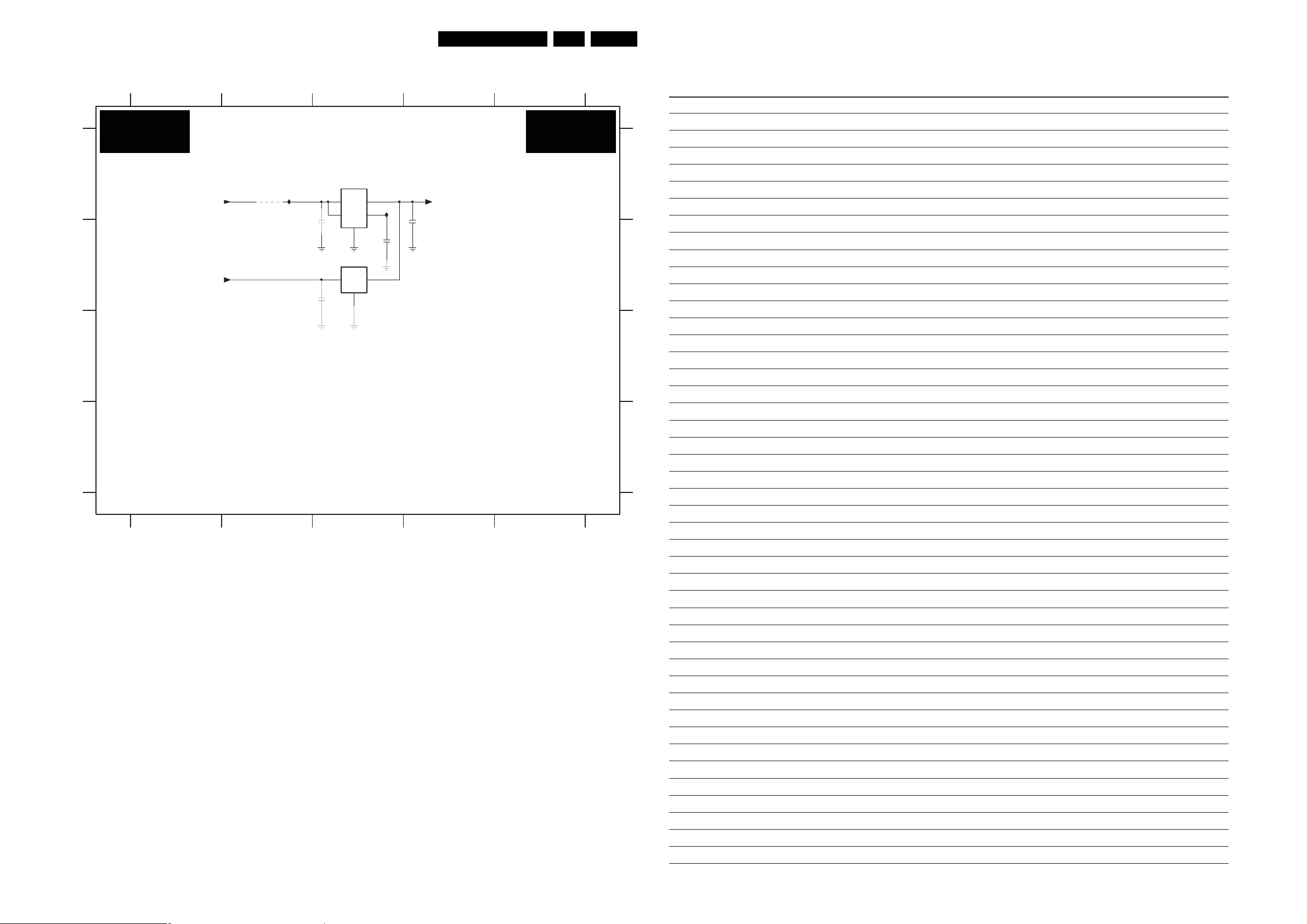
Circuit Diagrams and PWB Layouts
DFI Panel: Supply
2F17 B3 2F18 B4 2F19 B3 2F21 B3 7F35 A3 7F36 B3 9F13 A2 IF10 A2 IF1U A3
1234
80Q528.1A LA 7.
5
Personal Notes:
AB04 AB04
SUPPLY
A
B
C
+3V3
+12V
9F13
RES
IF10
1
RES
3
100n
2F17
32
RES
100n
2F21
7F35
LD3985M25
OUTIN
INH BP
COM
2
7F36
LD1117DT25
OUTIN
COM
1
RES
RES
5
IF1U
4
RES2F19
100n
2F18
RES
+2V5-STAB
1u0
A
B
C
D
3139 123 6188.2
D
H_16800_013.eps
1
2345
180407
E_06532_012.eps
131004
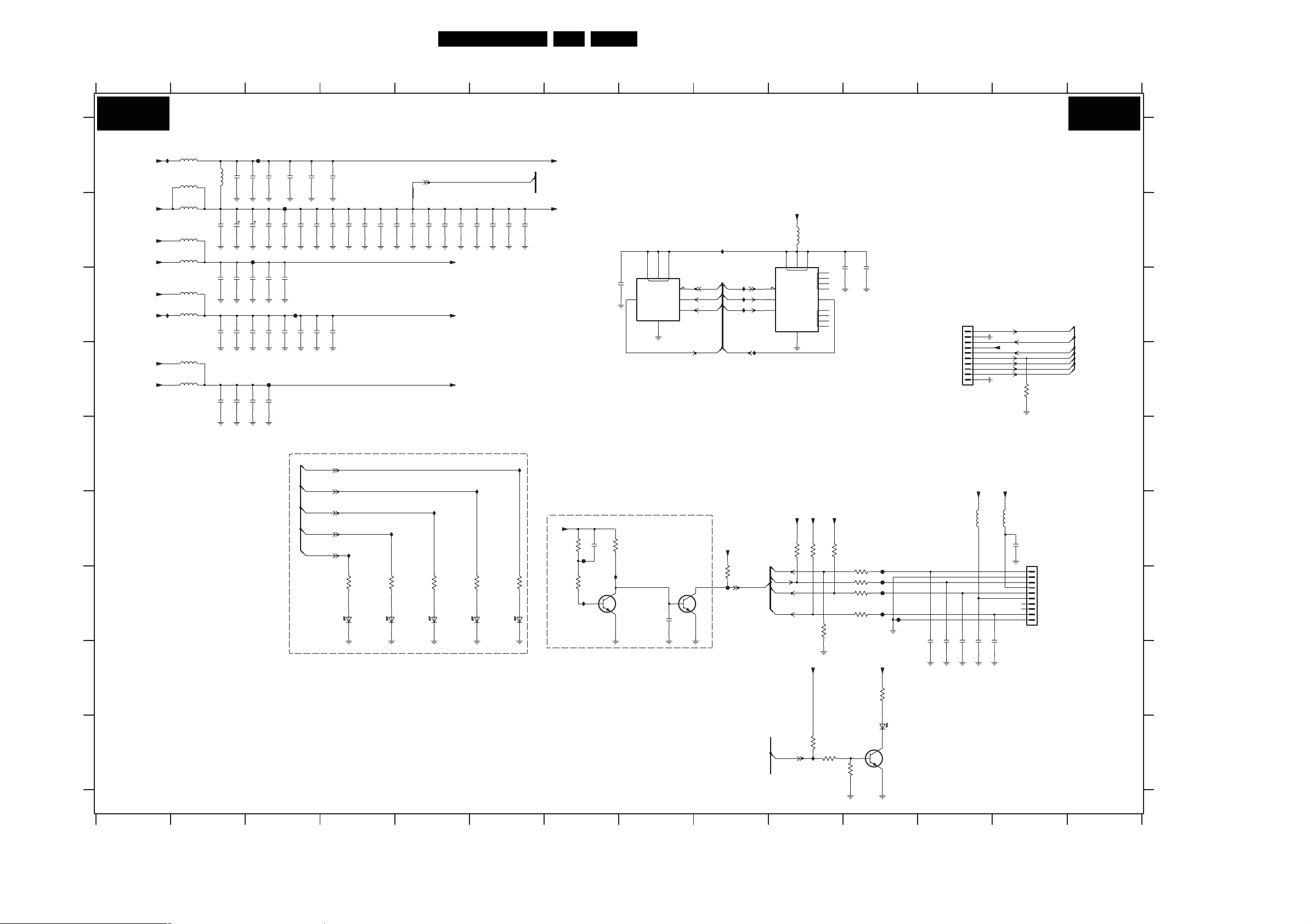
Circuit Diagrams and PWB Layouts
81Q528.1A LA 7.
DFI Panel: FPGA: Power & Control
12345678910
11 12 13 14
FPGA: POWER + CONTROL
AB05 AB05
RES
5F51
A
B
C
+2V5-STAB
D
+2V5-STAB
E
F
G
H
I
3139 123 6188.2
123
+1V2
+1V2
+2V5
+3V3
+2V5
+2V5
IFA1
30R
30R
30R
RES
5F23
30R
5F57
30R
5F24
30R
RES
30R
5F25
30R
RES
30R
30R
47u
1u0
2FJ8
2FLC
5F55
5F54
IFA5
5F58
5F26
5F53
2FHM
2FHN
4u7
4u7
1u0
100u 4V
10n
2FJ9
2FLD
2FH1
2FHL
2FHP
10n
10n
FF3J
2FLE
4u7
330u 6.3V
10n
2FJA
FF3G
2FHA
2FHT
2FHQ
10n
10n
10n
4u7
10n
2FJB
FF58
2FLF
2FH2
2FJP
2FHR
10n
10n
FF3H
1u0
10n
2FJC
+1V2-PLL
10n
2FH3
10n
2FJD
2FHC
10n
10n
2FJE
2FH4
2FHD
10n
10n
10n
2FJF
2FH5
2FHE
10n
SENSE+1V2-FPGA
cF01
+1V2-FPGA
10n
10n
2FHF
2FHG
10n
10n
2FHH
10n
2FHJ
2FHK
2FGF
10n
10n
10n
10n
2FGG
2FGJ
2FGH
+Vin-FPGA
+2V5out-FPGA
+2V5in-FPGA
2FGN
10n
10n
10n
2FGP
2FGM
IFA2
RES
RES
7F31
EPCS4SI8
3
7
8
10n
VCC
2FJJ
2
SCD
DATA
GND
1
CS_
Φ
DCLK
ASDI
4
nCSO
6
DCLK
5
ASDO
DATA0
nCSO
DCLK
ASDO
DATA0
EPCS16SI16N
IFA3
IFB1
IFB2
IFA4
+3V3
30R
5F52
7F30
7
15
CS
DCLK
ASDI
1
2
9
VCC
Φ
SCD
DATA
GND
10
10n
2FJK
10n
2FJL
ACTIVE SERIAL DEBUG-CONNECTOR
1F05
1
2
3
4
5
6
7
8
9
10
5-147279-2
+2V5
3F14
CONF-DONE
nCONFIG
DATA0
10K
DCLK
nCE
nCSO
ASDO
3
4
NC
5
6
816
11
12
13
NC
14
10n
2FHB
2FHS
FF3K
10n
RESERVED
MP-LED5
MP-LED4
MP-LED3
MP-LED2
MP-LED1
IFB6
IFB5
IFB4
IFB3
470R
SML-310
6F33
3F06
470R
SML-310
3F08
6F34
6F31
3F02
470R
SML-310
3F04
6F32
4567
470R
SML-310
IFB7
6F35
3F10
470R
SML-310
+3V3
3F11
3F83
+2V5 +2V5
+2V5 +2V5
RESERVED
6
7F34-1
1
+3V3
FF3P
3F81
10K
nCONFIG
1u0
10K
3F76
100K
2FJM
FF59
33K
IFA9
IFA7
3
5
7F34-2
BC847BS
4
2FJN
BC847BS
2
1u0
+2V5
1K0
RES
3F05
3F79
TCK
TDO
TMS
TDI
+3V3 +3V3
CONF-DONE
10K
IFA6
1K0
1K0
3F73
3F74
100K
3F78
3F86
1K0
3F82 100R
3F84
3F85
100R
3F75
100K
100R3F80
100R
FF3L
FF3M
FF3N
FF3Q
3K3
SML-310
7F32
BC847BW
3F72
6F30
FF69
2FLG
100p
2FLH
8 9 10 11 12
100p
2FLJ
100p
RES
5F49
2FLK
30R
30R
5F50
10n
2FJ7
1F00
1
2
FOR
3
4
5
DEBUG
6
7
8
9
10
5-147279-2
10n
100p
2FLL
13 14
H_16800_014.eps
180407
1F00 F13
1F05 C12
2FGF B5
2FGG B5
2FGH B5
2FGJ B6
2FGM B6
2FGN B6
2FGP B6
2FH1 A2
2FH2 A3
A
2FH3 A3
2FH4 A3
2FH5 A4
2FHA A3
2FHB B3
2FHC B3
2FHD B4
2FHE B4
2FHF B4
2FHG B4
2FHH B4
B
2FHJ B5
2FHK B5
2FHL B2
2FHM B2
2FHN C2
2FHP C2
2FHQ C3
2FHR C3
2FHS C3
2FHT B3
2FJ7 F13
2FJ8 C2
C
2FJ9 C2
2FJA C3
2FJB C3
2FJC C3
2FJD C3
2FJE C3
2FJF C4
2FJJ C8
2FJK C11
2FJL C11
2FJM F7
2FJN G8
D
2FJP B3
2FLC D2
2FLD D2
2FLE D2
2FLF D3
2FLG H12
2FLH H12
2FLJ H12
2FLK H12
2FLL H12
3F02 G4
E
3F04 G4
3F05 F10
3F06 G5
3F08 G6
3F10 G6
3F11 F7
3F14 D13
3F72 H11
3F73 I10
3F74 I10
3F75 I11
3F76 F7
F
3F78 F10
3F79 F10
3F80 G11
3F81 G9
3F82 G11
3F83 G7
3F84 G11
3F85 G11
3F86 G10
5F23 B2
5F24 C2
5F25 D2
G
5F26 D2
5F49 F12
5F50 F13
5F51 A2
5F52 B10
5F53 A2
5F54 B2
5F55 A2
5F57 B2
5F58 C2
6F30 I11
H
6F31 G4
6F32 G4
6F33 G5
6F34 G6
6F35 G6
7F30 B10
7F31 C8
7F32 I11
7F34-1 G9
7F34-2 G7
FF3G A3
FF3H B3
I
FF3J B3
FF3K C3
FF3L G11
FF3M G11
FF3N G11
FF3P G9
FF3Q G11
FF58 D3
FF59 G7
FF69 G11
IFA1 A1
IFA2 B9
IFA3 C9
IFA4 D9
IFA5 C1
IFA6 I10
IFA7 G8
IFA9 G7
IFB1 C9
IFB2 C9
IFB3 F4
IFB4 F4
IFB5 F5
IFB6 E6
IFB7 E6
cF01 B5

Circuit Diagrams and PWB Layouts
82Q528.1A LA 7.
DFI Panel: FPGA: DFI
1234567891011121314
AB06 AB06
A
B
C
D
CLK-OSC1B
E
F
CLK-OSC2B
MP-LED1
MM1-CKE
CTRL1-IN
CTRL2-IN
SCL-I2C4
SDA-I2C4
MP-LED4
MP-LED2
MP-LED3
COLOR-CLK
MP-LED5
COLOR6
COLOR7
COLOR2
COLOR3
FPGA DFI
1K0
RES
EP2C35F484C7N
3F40
3F49 47R
47R3FA0
7F18-3
M1
M2
M5
M6
N1
N2
P1
P2
N6
N5
N3
N4
P3
P5
P6
R1
R2
T1
T2
P4
R4
CLK2|LVDSCLK1p
CLK3|LVDSCLK1n
IO1|LVDS25p
IO2|LVDS25n
IO3|LVDS24p
IO4|LVDS24n
IO5|LVDS23p
IO6|LVDS23n
IO7|LVDS22p
IO8|LVDS22n
IO9|LVDS20p
IO10|LVDS20n
IO11|VREFB1N0
IO12|LVDS18p
IO13|LVDS18n
IO14|LVDS17p
IO15|LVDS17n
IO16|LVDS14p
IO17|LVDS14n
IO18|LVDS13p
IO19|LVDS13n
BANK1
IO39|PLL1_OUTp
IO40|PLL1_OUTn
IO20|LVDS12p
IO21|LVDS12n
IO22|LVDS10p
IO23|LVDS10n
IO24|LVDS8p
IO25|LVDS8n
IO26|LVDS7p
IO27|LVDS7n
IO28
IO29|VREFB1N1
IO30|LVDS6p
IO31|LVDS6n
IO32|LVDS5p
IO33|LVDS5n
IO34|LVDS2p
IO35|LVDS2n
IO36|LVDS0p
IO37|LVDS0n
IO38
+1V2-FPGA
U1
U2
R5
R6
V1
V2
3FA2 100R
T5
T6
T3
U3
W1
100R
W2
100R 3FA5
Y1
Y2
W3
W4
3FA4 100R
Y3
Y4
W5
U4
V4
IF06
IF01
+2V5-DDR2
+1V2-PLL
7F18-1
EP2C35F484C7N
G7
G8
G12
G16
H7
H8
H12
H13
H16
J10
J11
J12
J13
K8
K9
K14
L7
L8
L9
L14
L16
1K0
RES
3FA8
100R3FA1
3FA6
3FAA
33R
VCCINT1
VCCINT2
VCCINT3
VCCINT4
VCCINT5
VCCINT6
VCCINT7
VCCINT8
VCCINT9
VCCINT10
VCCINT11
VCCINT12
VCCINT13
VCCINT14
VCCINT15
VCCINT16
VCCINT17
VCCINT18
VCCINT19
VCCINT20
VCCINT21
+1V2-FPGA
IF15
IF16
SCL-AMBI-3V3
SDA-AMBI-3V3
LCD-PWR-ON
CLK-VIDEO-PLL
E5
U17
VCCD_PLL4
VCCINT22
M9
M14
COLOR0
COLOR1
COLOR8
COLOR9
SS-S0
SS-S1
COLOR5
MM2-CKE
COLOR4
CTRL1-FPGA
CTRL2-FPGA
SS-OFF
CTRL3-FPGA
CTRL4-FPGA
CLK-VIDEO
U6
F17
U16
VCCD_PLL1
VCCD_PLL2
VCCD_PLL3
VCCINT24N9VCCINT25
VCCINT23
M15
N14
E6
U7
F16
VCCA_PLL2
VCCA_PLL3
VCCA_PLL4
VCCINT26
VCCINT27
VCCINT28
N15
P10
P11
W6
V10
Y11
VCCIO8_4
VCCIO8_5
VCCA_PLL1
VCC
VCCINT30
VCCINT31
VCCINT29
P12
P13
P14
ASDO
nCSO
RXEB+
RXEB-
RXED+
RXEDRXEA+
RXEA-
RXOA+
RXOA-
RXEC+
RXECRXOB+
RXOBRXOE+
RXOERXECLK+
RXECLK-
T9
Y12
AB2
VCCIO8_2
VCCIO8_3
VCCIO7_5
VCCIO8_1
VCCINT32
VCCINT33
VCCINT34
VCCINT35
R7
R8
R10
EP2C35F484C7N
IF02
V13
W17
VCCIO7_3
VCCIO7_4
VCCINT36
VCCINT37
R12
R15
T14
T19
AB21
VCCIO7_1
VCCIO7_2
VCCINT38T7VCCINT39
R16
T8
7F18-4
C4
C3
D3
D4
D5
D6
E3
E4
C1
C2
F4
G6
G5
F3
D1
D2
G3
H4
H5
H6
E1
E2
P16
M20
VCCIO6_2
VCCIO6_3
VCCIO6_4
VCCIO6_1
VCCIO5_4
VCCIO5_3
VCCIO5_2
VCCIO5_1
VCCIO4_5
VCCIO4_4
VCCIO4_3
VCCIO4_2
VCCIO4_1
VCCIO3_5
VCCIO3_4
VCCIO3_3
VCCIO3_2
VCCIO3_1
VCCIO2_3
VCCIO2_2
VCCIO2_1
VCCIO1_4
VCCIO1_3
VCCIO1_2
VCCIO1_1
VCCINT41
VCCINT42
VCCINT40
T12
T15
IO1|ASDO
IO2|nCSO
IO3|LVDS48p
IO4|LVDS48n
IO5|PLL3_OUTp
IO6|PLL3_OUTn
IO7|LVDS47p
IO8|LVDS47n
IO9|LVDS46p
IO10|LVDS46n
IO11|VREFB2N0
IO12|LVDS43p
IO13|LVDS43n
IO14
IO15|LVDS39p
IO16|LVDS39n
IO17|LVDS38p
IO18|LVDS38n
IO19|LVDS37p
IO20|LVDS37n
IO21|LVDS36p
IO22|LVDS36n
+2V5-DDR2
+2V5out-FPGA
AA22
L20
J16
G19
B22
G14
E13
D17
C12
A21
G9
E10
C11
C6
A2
L3
B1
T4
P7
M3
AA1
BANK2
IO25|VREFB2N1
CLK0|LVDSCLK0p
CLK1|LVDSCLK0n
J7
IO23|LVDS35p
IO24|LVDS35n
IO26|LVDS30p
IO27|LVDS30n
IO28|LVDS29p
IO29|LVDS29n
IO30|LVDS28p
IO31|LVDS28n
IO32|LVDS27p
IO33|LVDS27n
IO34|LVDS26p
IO35|LVDS26n
DCLK|DCLK
DATA0|DATA0
nCONFIG
TMS
TDO
F6
G11
GND1
G15
GND2
H9
GND3
H10
GND4
H11
GND5
H14
GND6
H15
GND7
J8
GND8
J9
GND9
J14
GND10
J15
GND11
K10
GND12
K11
GND13
K12
GND14
K13
GND15
K15
GND16
L10
GND17
L11
GND18
L12
GND19
L13
GND20
L15
GND21
M7
GND22
M8
GND23
D12
CLK10|LVDSCLK5n
E12
CLK11|LVDSCLK5p
B11
IO1|LVDS70n
A11
IO2|LVDS70p
E11
IO3|LVDS69n
D11
IO4|LVDS69p
B10
IO5|LVDS68n
A10
IO6|LVDS68p
F11
IO7|LVDS67n
F10
IO8|LVDS67p
C10
IO9|VREFB3N0
B9
IO10|LVDS65n
A9
IO11|LVDS65p
E9
IO12|LVDS62n
D9
IO13|LVDS62p
B8
IO14|LVDS60n
A8
IO15|LVDS60p
V7
GNDA_PLL1
GND24
M10
V16
M11
T17
V18
GNDA_PLL4
GNDD_PLL4
GNDG_PLL4
GND26
GND27
GND25
M12
M13
BANK3
F18
E16
E17
GNDA_PLL2F7GNDA_PLL3
GNDD_PLL2
GNDG_PLL2F5GNDG_PLL3
GND28N8GND29
GND30
M16
N10
IO16|LVDS59n
IO17|LVDS59p
IO18|LVDS58n
IO19|LVDS58p
IO20|LVDS57n
IO21|LVDS57p
IO22|LVDS56p
IO24|LVDS54p
IO25|VREFB3N1
IO26|LVDS52n
IO27|LVDS52p
IO28|LVDS51n
IO29|LVDS51p
IO30|LVDS50n
IO31|LVDS50p
IO32|LVDS49p
IO33|LVDS49n
7F18-2
EP2C35F484C7N
+2V5out-FPGA
+2V5-DDR1
+2V5in-FPGA
+Vin-FPGA
7F18-5
VREF-FPGA1
EP2C35F484C7N
9F02
1n0
2F36
F1
RXEE+
F2
RXEEH3
G1
G2
J6
J5
H1
RXOC+
H2
RXOC-
J3
J4
J1
RXOD+
J2
RXOD-
K5
TDI
K2
TCK
K6
L5
L6
K4
K1
nCE
L1
L2
L4
TDI
TCK
TMS
TDO
DCLK
DATA0
RXOCLK+
RXOCLKnCONFIG
nCE
PLL2-OUT
MM1-A4
MM1-DQS3
MM1-D29
MM1-D27 MM1-D20
MM1-D28
MM1-D25
MM1-D26
MM1-D24
MM1-D31
MM1-D30
MM1-A3
MM1-A2
MM1-A1
MM1-DQS2
GNDD_PLL3
GND31
GND32
N11
N12
IO23
V5
U5
GNDG_PLL1
GND
GND33P8GND34P9GND35
N13
B7
A7
F9
E8
D8
C9
D7
F8
E7
C7
B6
A6
B5
A5
B4
A4
A3
B3
Y8
Y15
W19
GND80
GND81
GND79
GNDD_PLL1
GND37
GND38
GND36
R9
R11
P15
2F37
W10
W13
GND77
GND78
GND39
GND40
R13
R14
VREF-FPGA1
IF41
1n0
V17
GND76
GND41
T11
T16
V3
GND74V6GND75
GND43
GND42
A1
T13
T20
GND73
GND44
A22
AA2
MM1-D17
MM1-D18
MM1-D23
MM1-D21
MM1-D19
MM1-D22
MM1-D16
MM1-A0
MM1-BA1
MM1-A10
MM1-BA0
MM1-RAS
MM1-CS0
MM1-CAS
MM1-WE
T10
GND72
GND71
GND45
GND46
AA21
GND70
GND69
GND68
GND67
GND66
GND65
GND64
GND63
GND62
GND61
GND60
GND59
GND58
GND57
GND56
GND55
GND54
GND53
GND52
GND51
GND50
GND49
GND48
GND47
AB22
R3
N19
N16
N7
M4
K19
K16
K7
K3
H20
G13
G10
G4
F19
D18
D13
D10
C15
C8
C5
B21
B2
AB1
7F18-6
MM1-CLK-
MM1-CLK+
MM1-D13
MM1-D14
MM1-D15
MM1-D12
MM1-A11
MM1-A12
VREF-FPGA1
MM1-D11
MM1-D10
MM1-D9
MM1-D8
MM1-A8
MM1-A9
MM1-DQS1
EP2C35F484C7N
C18
C17
B20
A20
B19
A19
B18
A18
C16
D16
E15
D15
C14
F15
B17
A17
1n0
2F38
IO1|LVDS94n
IO2|LVDS94p
IO3|LVDS93n
IO4|LVDS93p
IO5|LVDS92n
IO6|LVDS92p
IO7|LVDS91n
IO8|LVDS91p
IO9|VREFB4N0
IO10|LVDS89n
IO11|LVDS89p
IO12|LVDS85n
IO13|LVDS85p
IO14|LVDS84p
IO15|LVDS82n
IO16|LVDS82p
BANK4
IO25|VREFB4N1
CLK8|LVDSCLK4n
CLK9|LVDSCLK4p
IO17|LVDS80n
IO18|LVDS80p
IO19|LVDS79n
IO20|LVDS79p
IO21|LVDS78n
IO22|LVDS78p
IO23|LVDS77n
IO24|LVDS77p
IO26|LVDS75n
IO27|LVDS73n
IO28|LVDS73p
IO29|LVDS71n
IO30|LVDS71p
E14
D14
F14
F13
B16
A16
B15
A15
C13
F12
B14
A14
B13
A13
B12
A12
2F39
IF03
1n0
IF38
VREF-FPGA1
CLK-SYSTEM-SS
MM1-D4
MM1-D5
MM1-D6
MM1-D0
MM1-D1
MM1-D2
MM1-D3
MM1-D7
MM1-A6
MM1-A7
MM1-A5
MM1-DQS0
CLK-OSC1A
A
B
C
D
E
F
2F36 F8
2F37 F10
2F38 F12
2F39 F13
2F40 I8
2F41 I10
2F42 I12
2F43 I13
3F40 E1
3F49 E1
3FA0 E1
3FA1 E3
3FA2 E3
3FA4 F3
3FA5 F3
3FA6 F3
3FA7 H7
3FA8 E3
3FAA F4
7F18-1 A4
7F18-10 G12
7F18-2 A8
7F18-3 E2
7F18-4 E5
7F18-5 E8
7F18-6 E12
7F18-7 G2
7F18-8 G5
7F18-9 G8
9F00 H14
9F01 G1
9F02 E8
9F03 G1
9F04 H7
9F05 I7
9F06 I7
9F07 H14
IF01 F3
IF02 E5
IF03 F13
IF04 I3
IF05 H5
IF06 F3
IF15 E4
IF16 E4
IF26 H5
IF27 I5
IF31 I7
IF36 G8
IF38 E14
IF39 G14
IF40 H8
IF41 F10
G
PLL2-OUT
CLK-VIDEO-SS
TX3F+
TX2DTX2D+ TX1CLK+
TX2CLK-
TX2CLK+
H
TX2F+
TX2ETX2E+
TX2CTX2C+
I
3139 123 6188.2
7F18-7
TX3F-
TX2F-
EP2C35F484C7N
L21
9F03
L22
9F01
RES
L19
L18
K21
K22
J21
J22
L17
K17
H21
H22
K18
J20
H19
K20
J19
J18
J17
G21
G22
BANK5
CLK5|LVDSCLK2n
CLK4|LVDSCLK2p
IO1|LVDS120n
IO2|LVDS120p
IO3|LVDS119n
IO4|LVDS119p
IO5|LVDS118n
IO6|LVDS118p
IO7|LVDS117n
IO8|LVDS117p
IO9|LVDS116n
IO10|LVDS116p
IO11
IO12|LVDS114n
IO13|LVDS114p
IO14|VREFB5N1
IO15|LVDS111n
IO16|LVDS111p
IO17
IO18|LVDS109n
IO19|LVDS109p
IO20|LVDS107n
IO21|LVDS107p
IO22|LVDS106n
IO23|LVDS106p
IO24|LVDS104n
IO25|LVDS104p
IO26|LVDS103n
IO27|LVDS103p
IO28|LVDS102n
IO29|LVDS102p
IO30|VREFB5N0
IO31|LVDS100n
IO32|LVDS100p
IO33|LVDS99n
IO34|LVDS99p
IO35|LVDS96n
IO36|LVDS96p
IO37|LVDS95n
IO38|LVDS95p
IO39|PLL2_OUTp
IO40|PLL2_OUTn
F21
F22
H18
H17
E21
E22
D21
D22
G17
G18
G20
E20
F20
C21
C22
C19
C20
D19
D20
E19
E18
TX2B-
TX2B+
TX1F-
TX1F+
TX1CLK-
TX1CTX1C+
TX1E-
TX1E+
TX2A-
TX2A+
TX1A-
TX1A+
TX1BTX1B+
TX1DTX1D+
PLL2-OUT
IF04
TX4FTX4F+
TX4ETX4E+
TX4BTX4B+
TX4CLKTX4CLK+
TX4DTX4D+
TX4CTX4C+
TX4A-
TX4A+
TX3E-
1234
7F18-10
EP2C35F484C7N
IF05
IF26
IF27
7F18-8
Y18
V19
W20
Y19
Y20
W18
U18
T18
U19
V20
U20
W21
W22
R17
Y21
Y22
V21
V22
U21
U22
R18
M22
BANK6
IO1
IO2|LVDS142n
IO3|LVDS142p
IO4|LVDS141n
IO5|LVDS141p
IO6
IO7|PLL4_OUTn
IO8|PLL4_OUTp
IO9|LVDS140n
IO10|LVDS140p
IO11|VREFB6N1
IO12|LVDS137n
IO13|LVDS137p
IO14|LVDS135p
IO15|LVDS133n
IO16|LVDS133p
IO17|LVDS132n
IO18|LVDS132p
IO19|LVDS131n
IO20|LVDS131p
IO21|LVDS130n
CLK6|LVDSCLK3p
IO22|LVDS130p
IO23|LVDS129n
IO24|LVDS129p
IO25|LVDS127n
IO26|LVDS127p
IO27|LVDS126n
IO28|LVDS126p
IO29|VREFB6N0
IO30|LVDS124n
IO31|LVDS124p
IO32|LVDS123n
IO33|LVDS123p
nSTATUS
CONF_DONE
MSEL1
MSEL0
IO34|LVDS122n
IO35|LVDS122p
IO36|LVDS121n
IO37|LVDS121p
CLK7|LVDSCLK3n
7F18-9
MM2-DQS3
MM2-A1
MM2-A0
MM2-D26
VREF-FPGA2
MM2-D24
MM2-D27
MM2-D25
MM2-D28
MM2-D30
MM2-D31
MM2-D29
MM2-A10
EP2C35F484C7N
IF36
IF40
2F40
100n
W12
V12
AB12
AA12
AB13
AA13
U13
Y13
AB14
AA14
AB15
AA15
AB16
AA16
W14
V14
BANK7
CLK13|LVDSCLK6p
CLK12|LVDSCLK6n
IO1|LVDS166p
IO2|LVDS166n
IO3|LVDS164p
IO4|LVDS164n
IO5|LVDS162n
IO6|VREFB7N1
IO7|LVDS160p
IO8|LVDS160n
IO9|LVDS159p
IO10|LVDS159n
IO11|LVDS158p
IO12|LVDS158n
IO13|LVDS157p
IO14|LVDS157n
IO15|LVDS155p
IO16|LVDS155n
IO17|LVDS153p
IO18|LVDS152p
IO19|LVDS152n
IO20|LVDS148p
IO21|LVDS148n
IO22|VREFB7N0
IO23|LVDS146p
IO24|LVDS146n
IO25|LVDS145p
IO26|LVDS145n
IO27|LVDS144p
IO28|LVDS144n
IO29|LVDS143p
IO30|LVDS143n
AB17
AA17
AB18
AA18
AB19
AA19
AB20
AA20
MM2-DQS2
2F41
MM2-RAS
MM2-BA1
MM2-D23
MM2-D22
MM2-D19
MM2-D18
VREF-FPGA2
MM2-CS0
MM2-BA0
MM2-D21
MM2-D20
MM2-D16
MM2-CAS
MM2-WE
100n
U14
Y14
W15
Y16
U15
V15
Y17
W16
R19
P17
P18
T21
T22
R21
R22
R20
P20
P19
P21
P22
N20
N18
N17
M17
9F04
N21
N22
M19
M18
M21
IF31
3FA7
10K
TX3E+
TX3D-
TX3D+
TX3CLK-
TX3CLK+
TX3C-
TX3C+
nSTATUS
CONF-DONE
MSEL1
TX3B-
TX3B+
TX3A-
TX3A+
RES
9F05
9F06
+3V3
+3V3
MM2-A11
MM2-CLK+
MM2-CLK-
MM2-A7
MM2-A6
MM2-A8
MM2-A9
VREF-FPGA2
MM2-A5
MM2-D14
MM2-D13
MM2-D10
MM2-D11
MM2-D9MM2-D17
MM2-D8
MM2-D12
MM2-D15
EP2C35F484C7N
AA3
AB3
AB4
AA4
Y5
Y6
AB5
AA5
Y7
U8
AB6
AA6
V8
W7
W8
V9
AB7
AA7
100n
2F42
IO1|LVDS188n
IO2|LVDS188p
IO3|LVDS187p
IO4|LVDS187n
IO5|LVDS186p
IO6|LVDS186n
IO7|LVDS185p
IO8|LVDS185n
IO9|VREFB8N1
IO10|LVDS183p
IO11|LVDS181p
IO12|LVDS181n
IO13|LVDS180p
IO14|LVDS180n
IO15|LVDS179p
IO16|LVDS179n
IO17|LVDS178p
IO18|LVDS178n
BANK8
IO19|LVDS177p
IO20|LVDS177n
IO21|LVDS175p
IO22|LVDS175n
IO23|LVDS172p
IO24|LVDS172n
IO25|VREFB8N0
IO26|LVDS170p
IO27|LVDS170n
IO28|LVDS169p
IO29|LVDS169n
IO30|LVDS168p
IO31|LVDS168n
IO32|LVDS167p
IO33|LVDS167n
CLK15|LVDSCLK7p
CLK14|LVDSCLK7n
W11
AB10
AA10
AB11
AA11
Y9
W9
U9
2F43
IF39
VREF-FPGA2
9F07
9F00
100n
U10
AB8
AA8
Y10
AB9
AA9
V11
U11
U12
MM2-DQS1MM2-A12
MM2-A4
MM2-A3
MM2-D1
MM2-D0
MM2-D3
MM2-D2
MM2-D6
MM2-D7
MM2-D4
MM2-D5
MM2-DQS0
MM2-A2
CLK-VIDEO-PLL
CLK-VIDEO-SS
H_16800_015.eps
180407
5 6 7 8 9 1011121314
G
H
I
Circuit Diagrams and PWB Layouts
83Q528.1A LA 7.
DFI Panel: DDR A
123
456789101112
DDR A
AB07 AB07
A
B
C
D
G
H
10n
2F5A
MM1-A0
MM1-A1
MM1-A2
MM1-A3
MM1-A4
MM1-A5
MM1-A6
MM1-A7
MM1-A8
MM1-A9
MM1-A10
MM1-A11
MM1-BA0
MM1-BA1
VREF-DDR1
MM1-CLK-
MM1-CLK+
MM1-CKE
MM1-CS0
MM1-RAS
MM1-CAS
MM1-WE
2F5B
10n
2F5P
3F4A
220R
7CA2
EDD1216AATA-5B-E
29
30
31
32
35
36
37
38
39
40
28
41
26
27
47
100n
49
46
45
44
24
23
22
21
+2V5-DDR1
11833391555
VDD
0
1
2
3
4
5
6
A
7
8
9
10
11
AP
0
BA
L
DM
U
VREF
CLK
CLK
CKE
CS
RAS
CAS
WE
VSS
344866612
Φ
DDR
SDRAM
2Mx16
+2V5-DDR1
VDDQ
VSSQ
52
+2V5-DDR1
10n
10n
10n
2F5H
10n
61
14
17
19
25
NC
43
50
53
42
2
0
4
1
5
2
7
3
8
4
10
5
11
6
13
D
71
54
8
5620
9
57
10
59
11
60
12
62
13
63
14
65
15
16
L
51
DQS
U
58
64
10n
2F5D
2F5C
DQ1(0)
DQ1(1)
DQ1(2)
DQ1(3)
DQ1(4)
DQ1(5)
DQ1(6)
DQ1(7)
DQ1(8)
DQ1(9)
DQ1(10)
DQ1(11)
DQ1(12)
DQ1(13)
DQ1(14)
DQ1(15)
DQS10 DQS10
DQS11
2F5E
10n
DQ1(0)
DQ1(1)
DQ1(2)
DQ1(3)
DQ1(4)
DQ1(5)
DQ1(6)
DQ1(7)
DQ1(8)
DQ1(9)
DQ1(10)
DQ1(11)
DQ1(12)
DQ1(13)
DQ1(14)
DQ1(15)
DQS11
2F5F
10u
3F4G
22R
3F4H
22R
3F4J
22R
3F4K
22R
3F4L
22R
3F4M
22R
3F4N
22R
3F4P
22R
3F4Q
22R
3F4R
22R
3F4S
22R
3F4T
3F4U
3F4V
3F4W
3F4Y
3F4Z
3F5A
MM1-D10
22R 22R
MM1-D11
22R
MM1-D12
22R
MM1-D13
22R
MM1-D14
22R
MM1-D15
22R
MM1-DQS0
22R
MM1-DQS1
MM1-D3
MM1-D2
MM1-D1
MM1-D0
MM1-D4
MM1-D5
MM1-D6
MM1-D7
MM1-D8
MM1-D9
MM1-A12MM1-A12
MM1-D17
MM1-D20
MM1-D23
MM1-D26
MM1-D29
2F5G
3F5B
3F5C
3F5D
3F5E
3F5F
3F5G
3F5H
3F5J
3F5K
3F5L
3F5M
3F5N
3F5P
3F5Q
3F5R
3F5S
3F6D 22R
22R
22R
22R
22R
22R
22R
22R
22R
22R
22R
22R
22R
22R
22R
22R
22R3F5T
2F5J
2F5K
DQ1(16)MM1-D16
DQ1(17)
DQ1(18)MM1-D18
DQ1(19)MM1-D19
DQ1(20)
DQ1(21)MM1-D21
DQ1(22)MM1-D22
DQ1(23)
DQ1(24)MM1-D24
DQ1(25)MM1-D25
DQ1(26)
DQ1(27)MM1-D27
DQ1(28)MM1-D28
DQ1(29)
DQ1(30)MM1-D31
DQ1(31)MM1-D30
DQS12MM1-DQS2
DQS13MM1-DQS3
10u
55
61
DQ1(16)
DQ1(17)
DQ1(18)
DQ1(19)
DQ1(20)
DQ1(21)
DQ1(22)
DQ1(23)
DQ1(24)
DQ1(25)
DQ1(26)
DQ1(27)
DQ1(28)
DQ1(29)
DQ1(30)
DQ1(31)
DQS12
DQS13
14
17
19
25
43
50
53
42
2
4
5
7
8
10
11
13
54
56 20
57
59
60
62
63
65
16
51
VDDQ
NC
0
1
2
3
4
5
6
D
71
8
9
10
11
12
13
14
15
L
DQS
U
VSSQ
58
64
E
F
+2V5-DDR1
3F4B
+2V5
SENSE+2V5
cF02
2F5T
6.3V330u
3F4C
2F5U
560R560R
100n
2F5Q
RES
100p
5F27
220R
5F28
220R
2F5R
100n
2F5S
IFD5
2F5W
IFD4
1u0
10n
2F5Y
VREF-DDR1
2F5Z
10n
16V22u
2F6A
+2V5-DDR1
560R
3F4D
FF56
1u0
2F6E
2F6C
10n
10n
2F6D
10n
10n
2F6B
2F6F
100n
2F6G
2FLM
100p
3F4E
10n
2FLN
560R
10n
VREF-FPGA1
10n
2FLP
2FLR
10n
2FLS
2FLT
2FLU
2FLV
10n
10n
10n
10n
9
15
Φ
DDR
SDRAM
2Mx16
12
52
+2V5-DDR1
+2V5-DDR1
33
3
VDD
VSS
6
66
7CA3
EDD1216AATA-5B-E
1
18
0
1
2
3
4
5
6
A
7
8
9
10
11
AP
0
BA
L
DM
U
VREF
CLK
CLK
CKE
CS
RAS
CAS
WE
34
48
10n
10n
2F5L
2F5M
29
30
31
32
35
36
37
38
39
40
28
41
26
27
47
49
46
45
44
24
23
22
21
100n2F5N
VREF-DDR1
3F4F
220R
MM1-CLK+
MM1-A0
MM1-A1
MM1-A2
MM1-A3
MM1-A4
MM1-A5
MM1-A6
MM1-A7
MM1-A8
MM1-A9
MM1-A10
MM1-A11
MM1-BA0
MM1-BA1
MM1-CLK-
MM1-CKE
MM1-CS0
MM1-RAS
MM1-CAS
MM1-WE
A
B
C
D
G
H
E
F
2F5A B2
2F5B B2
2F5C B5
2F5D B5
2F5E B5
2F5F B5
2F5G B7
2F5H B7
2F5J B7
2F5K B8
2F5L B10
2F5M B11
2F5N C10
2F5P C2
2F5Q G4
2F5R G4
2F5S G4
2F5T H3
2F5U H3
2F5W H4
2F5Y H4
2F5Z H5
2F6A H5
2F6B H5
2F6C H6
2F6D H6
2F6E G6
2F6F G6
2F6G G6
2FLM H6
2FLN H7
2FLP H7
2FLR H7
2FLS H8
2FLT H8
2FLU H8
2FLV H8
3F4A D2
3F4B F3
3F4C G3
3F4D F7
3F4E G7
3F4F D10
3F4G C5
3F4H C5
3F4J C5
3F4K C5
3F4L C5
3F4M C5
3F4N C5
3F4P C5
3F4Q C5
3F4R C5
3F4S C5
3F4T C5
3F4U D5
3F4V D5
3F4W D5
3F4Y D5
3F4Z D5
3F5A D5
3F5B C7
3F5C C7
3F5D C7
3F5E C7
3F5F C7
3F5G C7
3F5H C7
3F5J C7
3F5K C7
3F5L C7
3F5M C7
3F5N C7
3F5P D7
3F5Q D7
3F5R D7
3F5S D7
3F5T D7
3F6D D7
5F27 H4
5F28 H4
7CA2 B3
7CA3 B10
FF56 F6
IFD4 F4
IFD5 H4
cF02 H2
I
3139 123 6188.2
12
345678910
11 12
H_16800_016.eps
180407
I
Circuit Diagrams and PWB Layouts
84Q528.1A LA 7.
DFI Panel: DDR B
123456
AB08 AB08
DDR B
A
7CA0
29
30
31
32
35
36
37
38
39
40
28
41
26
27
47
49
46
45
44
24
23
22
21
0
1
2
3
4
5
6
7
8
9
10
11
AP
0
L
U
VREF
CLK
CLK
CKE
CS
RAS
CAS
WE
BA
DM
+2V5-DDR2
1183339
VDD
A
VSS
344866
10n
10n
2V39
2V42
EDD1216AATA-5B-E
B
C
D
MM2-A0
MM2-A1
MM2-A2
MM2-A3
MM2-A4
MM2-A5
MM2-A6
MM2-A7
MM2-A9
MM2-A10
MM2-A11
MM2-BA0
MM2-BA1
VREF-DDR2
MM2-CLK-
MM2-CLK+
MM2-CKE
MM2-CS0
MM2-RAS
MM2-CAS
MM2-WE
2V00 100n
3CE2
220R
Φ
DDR
SDRAM
2Mx16
6
+2V5-DDR2
15
VDDQ
VSSQ
125258
2V41
10n
10n
2CBD
2CBC
DQ2(0)
DQ2(1)
DQ2(2)
DQ2(3)
DQ2(4)
DQ2(5)
DQ2(6)
DQ2(7)
DQ2(8)
DQ2(9)
DQ2(10)
DQ2(11)
DQ2(12)
DQ2(13)
DQ2(14)
DQ2(15)
DQS20
DQS21
3CA0
3CA1
3CA2
3CA3
3CA4
3CA5
3CA6
3CA7
3CA8
3CA9
3CB0
3CB1
3CB2
3CB3
3CB4
3CB5
3CB6
3CB7
22R
22R
22R
22R
22R
22R
22R
22R
22R
22R
22R
22R
22R
22R
22R
22R
22R
22R
MM2-A12 MM2-A12
MM2-D3
MM2-D16
MM2-D2
MM2-D17
MM2-D1
MM2-D18
MM2-D0
MM2-D19
MM2-D4
MM2-D20
MM2-D5
MM2-D21
MM2-D6
MM2-D22
MM2-D7
MM2-D23
MM2-D8
MM2-D24
MM2-D9
MM2-D10
MM2-D11
MM2-D12
MM2-D13
MM2-D14
MM2-D15
MM2-DQS1
MM2-D25
MM2-D26
MM2-D27
MM2-D28
MM2-D29
MM2-D31
MM2-D30
MM2-DQS2MM2-DQS0
MM2-DQS3
55
61
14
17
19
25
NC
43
50
53
42
2
0
4
1
5
2
7
3
8
4
10
5
11
6
13
D
71
54
8
5620
9
57
10
59
11
60
12
62
13
63
14
65
15
16
L
51
DQS
U
64
2V40
10n
DQ2(0)
DQ2(1)
DQ2(2)
DQ2(3)
DQ2(4)
DQ2(5)
DQ2(6)
DQ2(7)
DQ2(8)
DQ2(9)
DQ2(10)
DQ2(11)
DQ2(12)
DQ2(13)
DQ2(14)
DQ2(15)
DQS20
DQS21
10u
E
+2V5-DDR2
F
560R
3CD6
3CD7
560R
2V45
100p
2V33
100n
2V46
FF91
1u0
VREF-DDR2
G
ICA0
100n
RES
5V01
220R
5V02
220R
2V04
16V22u
2V34
1n0
100p
2V05
2V52
10n
10n
2V53
2V54
10n
10n
2V55
10n
2FLY
2FLW
+2V5
6.3V
2V03
2V35
H
330u
7 8 9 10 11 12
9
15
Φ
DDR
SDRAM
2Mx16
12
52
+2V5-DDR2
3
33
VDD
VSS
6
66
+2V5-DDR2
7CA1
EDD1216AATA-5B-E
1
18
0
1
2
3
4
5
A
6
7
8
9
10
11
AP
0
BA
L
DM
U
VREF
CLK
CLK
CKE
CS
RAS
CAS
WE
34
48
10n
10n
2V50
2V51
29
30
31
32
35
36
37
38
39
40
28
41
26
27
47
49
46
45
44
24
23
22
21
3CD8
100n2V01
VREF-DDR2
3CE1
560R
FF92
MM2-A0
MM2-A1
MM2-A2
MM2-A3
MM2-A4
MM2-A5
MM2-A6
MM2-A7
MM2-A8
MM2-A9
MM2-A10
MM2-A11
MM2-BA0
MM2-BA1
MM2-CLK-
220R
MM2-CLK+
MM2-CKE
MM2-CS0
MM2-RAS
MM2-CAS
MM2-WE
VREF-FPGA2
+2V5-DDR2
2V44
22R3CD4
22R3CD5
10n
2CBH
2FGB
2CBK
DQ2(16)MM2-A8
DQ2(17)
DQ2(18)
DQ2(19)
DQ2(20)
DQ2(21)
DQ2(22)
DQ2(23)
DQ2(24)
DQ2(25)
DQ2(26)
DQ2(27)
DQ2(28)
DQ2(29)
DQ2(30)
DQ2(31)
DQS22
DQS23
10n
2FGC
10u
DQ2(16)
DQ2(17)
DQ2(18)
DQ2(19)
DQ2(20)
DQ2(21)
DQ2(22)
DQ2(23)
DQ2(24)
DQ2(25)
DQ2(26)
DQ2(27)
DQ2(28)
DQ2(29)
DQ2(30)
DQ2(31)
DQS22
DQS23
10n
14
17
19
25
43
50
53
42
2
4
5
7
8
10
11
13
54
56 20
57
59
60
62
63
65
16
51
10n
2FGE
2FGD
VDDQ
NC
0
1
2
3
4
5
6
D
71
8
9
10
11
12
13
14
15
L
DQS
U
VSSQ
58
64
+2V5-DDR2
10n
55
61
10n
22R
22R
22R
22R
22R
22R
22R
22R
22R
22R
22R
22R
22R
22R
22R
22R
10n
10n
2V43
3CB8
3CB9
3CC0
3CC1
3CC2
3CC3
3CC4
3CC5
3CC6
3CC7
3CC8
3CC9
3CD0
3CD1
3CD2
3CD3
10n
10n
2FLZ
2FGA
A
B
C
D
E
F
G
H
2CBC B5
2CBD B5
2CBH B7
2CBK B7
2FGA H7
2FGB H7
2FGC H8
2FGD H8
2FGE H8
2FLW H6
2FLY H6
2FLZ H7
2V00 C2
2V01 C10
2V03 H3
2V04 H4
2V05 H4
2V33 G4
2V34 H4
2V35 H3
2V39 B2
2V40 B4
2V41 B5
2V42 B2
2V43 B7
2V44 B7
2V45 G3
2V46 G4
2V50 B10
2V51 B10
2V52 H5
2V53 H5
2V54 H6
2V55 H6
3CA0 C5
3CA1 C5
3CA2 C5
3CA3 C5
3CA4 C5
3CA5 C5
3CA6 C5
3CA7 C5
3CA8 C5
3CA9 C5
3CB0 C5
3CB1 C5
3CB2 C5
3CB3 D5
3CB4 D5
3CB5 D5
3CB6 D5
3CB7 D5
3CB8 C7
3CB9 C7
3CC0 C7
3CC1 C7
3CC2 C7
3CC3 C7
3CC4 C7
3CC5 C7
3CC6 C7
3CC7 C7
3CC8 C7
3CC9 C7
3CD0 C7
3CD1 D7
3CD2 D7
3CD3 D7
3CD4 D7
3CD5 D7
3CD6 F3
3CD7 G3
3CD8 H10
3CD9 H10
3CE1 D10
3CE2 D2
5V01 G4
5V02 H4
7CA0 B3
7CA1 B10
FF91 F4
FF92 H10
ICA0 G4
I
3139 123 6188.2
560R
3CD9
1 34567891011
2
H_16800_017.eps
12
I
180407

Circuit Diagrams and PWB Layouts
85Q528.1A LA 7.
DFI Panel: Display Interfacing
1F04 D11
1F80 G13
1F81 G14
1F82 G14
1F83 G14
1M59 F15
2F2A D5
2F2B D3
2F2C B11
2F2D A12
2F2E F5
2F2F F6
2F2G F6
2F2H F5
2F2I B6
2F2K C13
2F2L C14
2F2P E11
2F2Q F11
2F30 G12
2F32 H9
2F33 F9
2F34 B8
2F35 C8
2F45 F12
2F46 D2
2F53 G2
2F78 F2
2F95 B1
3F13 G10
3F15 H12
3F16 H12
3F17 F10
3F18 B2
3F19 B8
3F1W C3
3F1Y D4
3F1Z D6
3F20 C8
3F21 D5
3F22 D3
3F23 B12
3F24 B11
3F25 E6
3F27 F5
3F28 F5
3F29 F5
3F2A E5
3F2B E5
3F2C E6
3F2D B6
3F2F E5
3F2S B13
3F2T B13
123456789101112131415
AB09 AB09
DISPLAY-INTERFACING
A
+12V
+12V-SSB
B
C
+5V
D
100n
2F95
6F09
BZX384-C4V7
LCD-PWR-ON
5F10
220R
5F11 RES
220R
5F12
220R
1u0
FF2P
2F46
RES
RES
9F2I
7F07
RES
3F48
330R
6F10
3F18
4K7
SML-310
SI4835BDY
*
7F05
*
3F1W
47K
6F02
*
BZX384-C5V6
*
IF0H
SI3441BDV
*
2F2B
*
IF07
1u0
IF93
3F22
47R
VDISP-SWITCH
*
3F31
47R
3F1Y
47K
IF08
7F08
*
IF0F
2
3
BC847BW
IF0A
1
*
IF0G
E
2F78
RES
2F53
RES
IF0K
IF0L
IF0M
IF0N
IFD7
RES
3FJD
47R
100p
3FLB
RES
47R
100p
IF0P
9F2R
9F2S
9F24
*
9F2T
*
*
CTRL1-FPGA
CTRL2-FPGA
CTRL3-FPGA
F
G
H
CTRL4-FPGA
CTRL-SSB1
CTRL-SSB2
CTRL2-IN
CTRL1-IN
SCL-AMBI-3V3
SDA-AMBI-3V3
3F2F
47R
3F27
47R
3F28
47R
3F29
47R
*
*
*
*
3139 123 6188.2
12345
3F2V
10K
3F21
3F2V E5
3F31 E3
3F37 G11
3F38 F11
3F39 F11
3F3A G11
5F0K
220R
5F0L
220R
5F0M
220R
3F2D
2K2
IF09
*
10K
100n
2F2A
*
3F3B F11
3F3C G11
3F44 F12
3F45 G12
3F48 D2
3FH4 D10
3FH5 D11
3FJD F2
3FLB G2
5F0I B10
5F0J A10
5F0K B6
5F0L B6
5F0M B6
5F10 B2
5F11 B2
5F12 B2
5F13 F13
5F14 F13
5F15 F13
5F16 G13
5F17 G13
6F02 C3
6F04 B13
6F05 B12
6F07 B6
6F09 D1
6F10 B2
7F05 C4
7F07 B4
7F08 C5
7F09-1 F11 FF08 F13
7F09-2 G11
7F10 B10
9F16 H12
9F24 H3
*
*
3F1Z
FF1B
2F2I
*
100n
6F07
SML-310
*
10K
+VDISP
+3V3
SDA-I2C4-SSB
SCL-I2C4-SSB
*
2F34
2F35
3F19
SDA-I2C4
47R
10p
3F20
SCL-I2C4
47R
10p
*
+3V3
+3V3
SDA-I2C4
SCL-I2C4
9F26 H12
9F27 E13
9F28 F13
9F29 F13
9F2F C11
9F2G D11
+3V3
+5V
9F2H B11
9F2I B4
9F2N F11
9F2P G11
9F2R F3
9F2S G3
IF0S
RES
RES
IF0T
5F0J
120R
5F0I
120R
7F10
PCA9515ADP
RES
3SDA0 6SDA1
2SCL0 7SCL1
5EN
3FH4
9F2T H3
9F2U D11
9F2V E11
9F30 G13
9F31 G13
FF06 F12
RES
47R
+3V3
+5V
IF0B
VCC
GND
9F2F
9F2G
3FH5
47R
8
NC
4
RES
FF07 F12
FF09 H12
FF13 H13
FF17 E6
FF18 F6
FF19 F6
FF1A F6
FF1B B6
FF2P C2
IF07 D4
IF08 B4
I2C-BUFFER
9F2H
RES
100n
3F24
2F2C
RES
RES
1
IF0C
1F04
9F2U
9F2V
RES
56
RES
2F2D
RES
4K7
4K7
3F23
RES
1
FOR
2
3
DEBUG
4
*
100n
IF09 D5
IF0A D5
IF0B B11
IF0C C11
IF0D B12
IF0E B13
6F05
BAV99 COL
IF0D
IF0F C4
IF0G E4
IF0H D3
IF0K E2
IF0L F2
IF0M F2
RES
IF0E
3F2T
47R
IF0N F2
IF0P G2
IF0S B10
IF0T B10
IF18 F11
IF19 F11
BAV99 COL
2F2K
6F04
IF1A F11
IF1B G11
IF1C G11
IF1D G11
IF93 C3
IFD7 F2
RES
3F2S
47R
10p
2F2L
SDA-I2C4-DISP
SCL-I2C4-DISP
10p
AMBI-LIGHT BUFFER *
3F2A
2F2E
47R
3F2B
*
*
100p
2F2H
*
*
4K7
47R
47R
3F25
100p
3F2C
2F2G
FF17
*
*
FF18
FF19
FF1A
100p
100p
2F2F
*
*
6
CTRL-DISP1
CTRL-DISP2
CTRL-DISP3
CTRL-DISP4
7
2F2P
470p
3F39
10K
7F09-1
BC847BS
4K7
3F3B
IF19
2F2Q
470p
3F3A
10K
7F09-2
BC847BS
4K7
3F3C
IF1C
CTRL-SSB3
SCL-AMBI-3V3
CTRL-SSB4
SDA-AMBI-3V3
2F33
2F32
+3V3
3F17
47R
RES
100p
RES
3F13
RES
100p
RES
+3V3
47R
8 9 10 11
1
4
9F2N
9F2P
9F27
+5V
IF18
2
2K2
3F38
6
12
RES
IF1B
5
3
RES
IF1A
+5V
IF1D
3F44
FF06
2F45
100p
3F15
100R
9F16
3F16
100R
9F26
FF07
FF08
100p
2F30
RES
FF09
RES
FF13
100R
2K2
3F37
3F45
100R
+5V
+5V
5F13
120R
9F28
5F14
120R
9F29
5F15
120R
9F30
5F16
120R
9F31
5F17
120R
1F80
1F81
1F82
1F83
1M59
1
2
3
4
5
7
6
B5B-PH-SM4-TBT(LF)
12 13 14 15
TO
AMBI
LIGHT
H_16800_018.eps
180407
A
B
C
D
E
F
G
H

Circuit Diagrams and PWB Layouts
86Q528.1A LA 7.
DFI Panel: FPGA Ambilight
1234567
7F65-2
A7
A12
B4
D9
A14
B14
A13
B13
E11
D11
B11
C11
E10
D10
F9
E9
A9
A10
D8
C8
F8
E8
D7
E7
D6
C6
XC3S250E-4FTG256C
BANK0
IO
IO
VREF_0
IO_L01N_0
IO_L01P_0
IO_L03N_0
VREF_0
IO_L03P_0
IO_L04N_0
IO_L04P_0
IO_L05N_0
VREF_0
IO_L05P_0
IO_L06N_0
IO_L06P_0
IO_L08N_0
GCLK5
IO_L08P_0
GCLK4
IO_L09N_0
GCLK7
IO_L09P_0
GCLK6
IO_L11N_0
GCLK11
IO_L11P_0
GCLK10
IO_L12N_0
IO_L12P_0
IO_L14N_0
VREF0
IO_L14P_0
IO_L15N_0
IO_L15P_0
Φ
IO_L17N_0
VREF_0
IO_L17P_0
IO_L18N_0
IO_L18P_0
IO_L19N_0
HSWAP
IO_L19P_0
IP_L02N_0
IP_L02P_0
IP_L07N_0
IP_L07P_0
IP_L10N_0
GCLK9
IP_L10P_0
GCLK8
IP_L16N_0
IP_L16P_0
V CCO_0
A4
*
A5
C4
C5
B3
C3
C12
D12
C9
C10
B8
A8
E6
D5
A3
B6
B10
IP
C13
B7
C7
NC
B5
B12
F7
F10
AB10 AB10
A
B
C
FPGA AMBILIGHT
+2V5
5F31
120R
10n
100n
2F61
2F60
5F34
120R
5F32
RES
120R
100n
2F74
2F75
5F33
120R
100n
2F31
2F29
9F52
IF12
9F53
9F54
RES
RES
LD1117DT12
32
10n
RES
2F22
10n
2F20
2F62
7F01
COM
2F25
RES
2F63
10n
10n
2F26
10n
4u7
2F72
2F55
OUTIN
2F23
1
4u7
4u7
4V47u
+3V3
+2V5-STAB
+1V2-PF
+1V2
+3V3
+2V5
FF62
2F73
FF60
FF61
IF61
10n
2F27
10n
2F64
10n
2F54
10n
2F77
10n
2F65
2F28
10n
2F16
+1V2-PF
4u7
IF52
SDA-AMBI-3V3 SCL-AMBI-3V3
+3V3M
10n
10n
10n
10n
2F66
10n
2F93
10n
2F10
2F67
10n
10n
2F11
2F94
2F69
10n
10n
2F12
2F90
2F96
10n
2F13
10n
10n
10n
2F92
2F91
+2V5M
10n
10n
2F97
+1V2M
10n
3F6J
*
100R
IF74
D
XCF flash- RESERVED
+3V3M
3F6T
2F68
100R
3F6R
10K
3F6Q
3F6S
47R
100R
2F59
10p
E
MISO
CCLK
INIT
F
6F62
3F6U
+3V3M
470R
SML-310
G
FPGA-TDI
FPGA-TDO
H
I
FPGA-TMS
FPGA-TCK
LED1B
LED2B
LED3B
LED4B
LED5B
IF53
3F32
1K0
IF54
3F33
1K0
IF55
3F34
1K0
IF56
3F35
1K0
IF57
3F36
1K0
3F7D
RES
100R
6F63
SML-310
6F64
SML-310
6F65
SML-310
6F66
SML-310
6F67
SML-310
7F62
BC847BW
100R
100R
3F6V
3F6W
100K
100K
RES3F7C
3F7E RES
100R
3F7F
FF55
RES
FF52
330R
3F9A
3F9B
330R
FF51
3F6Z
100R
1
8
10
5
6
4
17
9F55
+3V3M
10n
47R
3FKV
100R
INT
D0
CLK
RESET
OE
CE
TMS
TCK
TDI
TDO
182019
FF54
100R
3FKW
2F76
+3V3M
+2V5M
OJ
VCC
GND
11
3F7A
10K
100R
3FKY
10n
7F60
XCF02SVOG20C
73
CF
13
CEO
2
9
12
14
NC
15
16
+2V5M
+2V5M
3F7B
IF69
3FKZ
2F57
1F03
9
10n
3F9J
47R
+2V5M
10K
3F9C
IF48
RES
nCONFIG DONE
9F40
10n
RES
2F70
10K
3F7G
DONE
47R
FF53
330R
3F7H
1
FOR
2
DEBUG
3
4
5
6
7
8
+2V5M
+2V5M
+2V5M
+2V5M
+2V5M
+2V5M
+2V5M
+2V5M
+1V2M
+1V2M
+1V2M
+1V2M
+1V2M
+1V2M
+1V2M
+1V2M
PROG-B
T15
D3
A15
A2
C14
B15
A6
A11
F1
F16
L1
L16
T6
T11
D4
D13
E5
E12
M5
M12
N4
N13
7F65-1
XC3S250E-4FTG256C
MAIN
DONE
PROG_B
TCK
TDI
TDO
TMS
VCCAUX
VCCINT
Φ
GND
3139 123 6188.2
1234
56789
8 9 10 11 12 13 14
3F9E
100R
9F41
COLOR7
COLOR9
COLOR-CLK
COLOR6
COLOR9
COLOR4
COLOR5
COLOR3
+3V3M
+3V3M
+3V3M
+3V3M
LED5B
INIT
CSO-B
MOSI
A1
A16
B9
F6
F11
G7
G8
G9
G10
H2
H7
H8
H9
H10
J7
J8
J9
J10
J15
K7
K8
K9
K10
L6
L11
R8
T1
T16
LED2B
LED1B
CLK-OSC2C
CLK-OSC1D
MISO
HIGH=SPI flash
LOW=XCF flash
+3V3
LED3B
LED4B
SDA-I2C4
SCL-I2C4
COLOR2 COLOR8
COLOR1
COLOR0
9F42
3F30
10R
33p
2F14
3F9F
3F03
100R
3F9M
RES
9F43
47R
47R
M14
D16
R15
IF77
R16
P15
IF78
P16
IF79
M16
N16
L15
L14
K12
K13
K14
K15
J16
K16
J13
J14
H14
H15
H11
H12
G16
G15
G14
G13
T8
IO
D5
T10
IO
M1
P13
IO
VREF_2
R4
IO
VREF_2
P4
IO_L01N_2
INIT_B
P3
IO_L01P_2
CSO_B
N5
IO_L03N_2
MOSI
CSI_B
P5
IF71
IO_L03P_2
DOUT
BUSY
T5
IO_L04N_2
T4
IO_L04P_2
N6
IO_L05N_2
M6
IO_L05P_2
P6
IO_L06N_2
R6
IO_L06P_2
L8
IO_L09N_2
D6
GCLK13
M8
IF72
IO_L09P_2
D7
GCLK12
P8
IF73
IO_L10N_2
D3
GCLK15
N8
IO_L10P_2
D4
GCLK14
N9
IO_L12N_2
10R
D1
GCLK3
P9
IO_L12P_2
D2
GCLK2
M9
IO_L13N_2
DIN
1K0
IF49
D0
L9
IO_L13P_2
M0
M10
IO_L15N_2
N10
IO_L15P_2
3F9G
P11
IO_L16N_2
A22
3F9H
R11
IO_L16P_2
A23
7F65-3
XC3S250E-4FTG256C
Φ
BANK1
IO
IO
VREF_1
IO_L01N_1
A15
IO_L01P_1
A16
IO_L02N_1
A13
IO_L02P_1
A14
IO_L04N_1
VREF_1
IO_L04P_1
IO_L06N_1
IO_L06P_1
IO_L07N_1
A11
IO_L07P_1
A12
IO_L08N_1
VREF_1
IO_L08P_1
IO_L09N_1
A9
RHCLK1
IO_L09P_1
A10
RHCLK0
IO_L10N_1
A7
|RHCLK3
TRDY1
IO_L10P_1
A8
RHCLK2
IO_L11N_1
A5
RHCLK5
IO_L11P_1
A6
RHCLK4
IRDY1
IO_L12N_1
A3
RHCLK7
IO_L12P_1
A4
RHCLK6
IO_L13N_1
A1
IO_L13P_1
A2
IO_L14N_1
A0
IO_L14P_1
7F65-4
XC3S250E-4FTG256C
Φ
BANK2
IO_L18N_2
IO_L18P_2
IO_L19N_2
IO_L19P_2
IO_L20N_2
IO_L20P_2
IP_L02N_2
IP_L02P_2
IP_L08N_2
IP_L08P_2
IP_L11N_2
IP_L11P_2
RDWR_B
IP_L17N_2
IP_L17P_2
VCCO_2
CCLK
VREF_2
GCLK1
GCLK0
IO_L15N_1
IO_L15P_1
IO_L16N_1
IO_L16P_1
IO_L18N_1
IO_L18P_1
IO_L19N_1
IO_L19P_1
VREF_1
VCCO_1
A20
A21
VS1
A18
VS2
A19
VS0
A17
M2
IP
NC
LDC0
LDC2
LDC1
HDC
F15
F14
F12
F13
D14
D15
C15
C16
H13
IP
B16
E14
G12
H16
IP
J11
J12
M13
E13
E16
L12
NC
L13
N14
N15
E15
G11
K11
M15
+3V3M
+3V3M
+3V3M
+3V3M
FACTORY
N12
P12
R13
3F07
3F09
T13
R14
9F44
P14
1K0
R3
3F12
T3
T7
R7
9F51
R9
T9
IF75
M11
N11
M7
T2
T12
T14
N7
P7
P10
R10
L7
+3V3M
L10
+3V3M
R5
+3V3M
R12
+3V3M
10p
2F58
RES
9F46
RES1K0
RES1K0
9F45
3F7S
10R
+3V3
CSO-B
WRITE
HOLD
MOSI
CCLK
CSO-B
WRITE
HOLD
CCLK
+3V3
+3V3
1
2
3
4
5
6
7
FF63
FF64
FF65
FF66
FF67
1F02
8
3F9K
4K7
9F36
9F37
FOR
USE
F5
N2
B2
B1
C2
C1
E4
E3
E1
D1
G4
G5
G2
G3
H6
H5
H4
H3
J3
J2
J4
J5
K1
J1
K3
K2
100R
FF85
9
2F71
M25P20-VMN
3F6K
100R
3F6L
100R
3F99
100R
3F41
FF80
30R 5F29
10n
7F61
5
6
1
3
7
IO
IO
VREF_3
IO_L01N_3
IO_L01P_3
IO_L02N_3
VREF_3
IO_L02P_3
IO_L03N_3
IO_L03P_3
IO_L05N_3
IO_L05P_3
IO_L06N_3
IO_L06P_3
IO_L07N_3
IO_L07P_3
IO_L08N_3
LHCLK1
IO_L08P_3
LHCLK0
IO_L09N_3
LHCLK3
IRDY2
IO_L09P_3
LHCLK2
IO_L10N_3
LHCLK5
IO_L10P_3
LHCLK4
TRDY2
IO_L11N_3
LHCLK7
IO_L11P_3
LHCLK6
IO_L12N_3
IO_L12P_3
IO_L13N_3
IO_L13P_3
100R
3F42
D
C
S
W
HOLD
7F65-5
XC3S250E-4FTG256C
Φ
BANK3
IO_L15N_3
IO_L15P_3
IO_L16N_3
IO_L16P_3
IO_L18N_3
IO_L18P_3
IO_L19N_3
IO_L19P_3
CSO-B
MOSI
MISO
CCLK
100R
100R
3F46
3F43
FPGA-TMS
FPGA-TDI
FPGA-TDO
FPGA-TCK
+3V3M
+3V3
30R
5F30
IF76
84
VCC
Φ
Q
2M
FLASH
VSS
2
10 11 12 13
VREF_3
VCCO
2F24
IP
IP
NC
FPGA-TDI
FPGA-TDO
FPGA-TMS
FPGA-TCK
PROG-B
100n
2F15
L5
K5
N1
M1
P1
P2
R1
R2
G1
D2
F2
H1
J6
K4
M3
N3
F3
F4
L2
L3
L4
M4
E2
G6
K6
M2
FF81
FF82
FF83
FF84
3F47
100R
FF50
3F6M
10R
FF68
33p
H_16800_019.eps
14
+3V3M
+3V3M
+3V3M
+3V3M
2F44
10p
2F50
10p
2F51
10p
2F52
10p
100p
MISO
2F56
180407
1F02 E12
7F01 C2
1F03 I5
7F60 E5
2F10 B3
7F61 H13
2F11 B4
7F62 G3
2F12 B4
7F65-1 F7
2F13 B4
7F65-2 A7
2F14 G9
7F65-3 A10
2F15 I13
7F65-4 E10
2F16 B3
7F65-5 A13
2F20 A2
9F36 H12
2F22 D2
2F23 D3
2F24 H13
2F25 B2
2F26 B3
2F27 B3
2F28 B3
2F29 B2
2F31 B2
2F44 E14
2F50 F14
2F51 F14
2F52 F14
2F54 D3
2F55 B2
2F56 F14
2F57 E5
2F58 F11
2F59 F3
2F60 A2
2F61 A2
2F62 A3
2F63 A3
2F64 A3
2F65 A3
2F66 A3
2F67 A4
2F68 E4
2F69 A4
2F70 G5
2F71 F12
2F72 B3
2F73 B3
2F74 B2
2F75 B2
2F76 I4
2F77 B3
2F90 A4
2F91 A4
2F92 A4
2F93 B3
2F94 B4
2F96 B4
2F97 B4
3F03 H9
3F07 F11
3F09 F11
3F12 G11
3F30 F8
3F32 H2
3F33 I2
3F34 I2
3F35 I2
3F36 I2
3F41 E12
3F42 E13
3F43 E13
3F46 E13
3F47 F14
3F6J A6
3F6K H12
3F6L I12
3F6M H14
3F6Q E2
3F6R E2
3F6S E3
3F6T E3
3F6U G2
3F6V G3
3F6W G3
3F6Z F4
3F7A F4
3F7B G4
3F7C H3
3F7D H2
3F7E H3
3F7F H3
3F7G H5
3F7H H5
3F7S F11
3F99 I12
3F9A I3
3F9B I3
3F9C F5
3F9E A8
3F9F H9
3F9G I9
3F9H I9
3F9J F5
3F9K H12
3F9M I9
3FKV H4
3FKW H4
3FKY H4
3FKZ H4
5F29 F13
5F30 H13
5F31 A2
5F32 B2
5F33 B2
5F34 A2
6F62 G2
6F63 H2
6F64 I2
6F65 I2
6F66 I2
6F67 I2
9F37 H12
9F40 G5
9F41 B8
9F42 F9
9F43 I9
9F44 F11
9F45 F11
9F46 F11
9F51 G11
9F52 C2
9F53 C2
9F54 C2
9F55 G4
FF50 F14
FF51 I3
FF52 H3
FF53 H5
FF54 H4
FF55 H4
FF60 A3
FF61 B3
FF62 B3
FF63 H12
FF64 I12
FF65 I12
FF66 I12
FF67 I12
FF68 I14
FF80 F13
FF81 E14
FF82 F14
FF83 F14
FF84 F14
FF85 F12
IF12 C2
IF48 F5
IF49 I9
IF52 A6
IF53 H2
IF54 I2
IF55 I2
IF56 I2
IF57 I2
IF61 C3
IF69 H4
IF71 G9
IF72 G9
IF73 H9
IF74 B6
IF75 G11
IF76 H13
IF77 A9
IF78 A9
IF79 B9
A
B
C
D
E
F
G
H
I

Circuit Diagrams and PWB Layouts
Layout DFI Panel (Top Side)
87Q528.1A LA 7.
3101 313 6188.2
H_16800_020.eps
180407
1F00 C1
1F02 C2
1F03 A1
1F04 A4
1F05 C3
1F13 C4
1F50 A4
1F51 A3
1F52 A1
1M09 C4
1M12 C3
1M59 C3
1M90 C4
2F15 C1
2F22 C4
2F23 C4
2F24 C1
2F29 C2
2F2B A4
2F2C A4
2F2D A4
2F2E A2
2F2F A2
2F2G A2
2F2H A2
2F2I A3
2F2K A2
2F2L A2
2F30 C3
2F34 A4
2F35 A4
2F45 C2
2F46 A4
2F54 C4
2F57 C1
2F59 C1
2F5P A1
2F5Z B1
2F68 C1
2F76 A1
2F95 A4
2FD1 C2
2FD2 C2
2FHL C4
2FJ7 C1
2FJJ C3
2FJK C3
2FJL C3
2FLG C1
2FLH C1
2FLJ C1
2FLK C1
2FLL C1
2U01 B4
2U02 C4
2U03 B4
2U06 B4
2U09 C4
2U10 B4
2U12 B4
2U13 C4
2U14 B4
2U16 C4
2U21 B4
2U22 B4
2U25 C4
2U32 B4
2U35 B4
2U38 A4
2U41 B4
2V34 B3
3CA0 B3
3CA1 B3
3CA2 B3
3CA3 B3
3CA4 B3
3CA5 B3
3CA6 B3
3CA7 B3
3CA8 B3
3CA9 B3
3CB0 B3
3CB1 B3
3CB2 B3
3CB3 B3
3CB4 B3
3CB5 B3
3CB6 B3
3CB7 B3
3CB8 A3
3CB9 A3
3CC0 A3
3CC1 A3
3CC2 A3
3CC3 A3
3CC4 A3
3CC5 A3
3CC6 A3
3CC7 A3
3CC8 A3
3CC9 A3
3CD0 A3
3CD1 A3
3CD2 A3
3CD3 A3
3CD4 A3
3CD5 A3
3CE1 A3
3CE2 B3
3F05 C1
3F14 C3
3F15 C3
3F16 C3
3F18 A4
3F19 A4
3F1W A4
3F20 A4
3F22 A4
3F23 A4
3F24 A4
3F25 A2
3F26 C2
3F27 A2
3F28 A2
3F29 A2
3F2A A2
3F2B A2
3F2C A2
3F2D A4
3F2F A2
3F2S A2
3F2T A2
3F44 C2
3F45 C3
3F48 A4
3F4A A1
3F4F B1
3F4G A2
3F4H A1
3F4J A1
3F4K A1
3F4L A1
3F4M A1
3F4N A1
3F4P A1
3F4Q A1
3F4R A1
3F4S A1
3F4T A1
3F4U A1
3F4V A1
3F4W A1
3F4Y A1
3F4Z A1
3F50 A2
3F51 A2
3F52 A2
3F53 A2
3F54 A2
3F55 A2
3F56 A2
3F57 A2
3F58 A2
3F59 A2
3F5A A1
3F5B B2
3F5C B1
3F5D B1
3F5E B1
3F5F B1
3F5G B1
3F5H B1
3F5J B1
3F5K B1
3F5L B1
3F5M B1
3F5N B1
3F5P B1
3F5Q B1
3F5R B1
3F5S B2
3F5T B1
3F5U A2
3F5V A2
3F5W A2
3F5Y A2
3F5Z A2
3F60 A2
3F61 A2
3F62 A2
3F63 A2
3F64 A2
3F65 A2
3F66 A2
3F67 A2
3F68 A2
3F69 A2
3F6A A2
3F6B A2
3F6C A2
3F6D B1
3F6K C1
3F6L C1
3F6M C1
3F6Q B1
3F6R B1
3F6S C1
3F6T C1
3F6U C1
3F6V C1
3F6W C1
3F6Z B1
3F70 A2
3F71 A2
3F78 C1
3F79 C1
3F7A B1
3F7B C1
3F7G C1
3F7H C1
3F7J A3
3F7K A3
3F7L A3
3F7M A3
3F7N A3
3F7P A3
3F7Q A3
3F7R A3
3F80 C1
3F82 C1
3F84 C1
3F85 C1
3F86 C1
3F87 B2
3F88 B2
3F89 B2
3F8A A2
3F8B A2
3F8C A2
3F8D A2
3F8E A2
3F8F A2
3F8G A2
3F8H A2
3F8J A2
3F8K A2
3F8L A2
3F8M A2
3F8N A2
3F8P A2
3F8Q A2
3F8R A2
3F8S A2
3F8T A2
3F8U A2
3F8V A3
3F8W A2
3F8Y A3
3F8Z A3
3F90 B2
3F91 B2
3F92 A2
3F93 A2
3F94 A2
3F95 A2
3F96 B2
3F97 B2
3F98 B2
3F99 C1
3F9A C1
3F9B B1
3F9J C1
3F9K C1
3F9N A3
3F9P A3
3F9Q A3
3F9R A3
3F9S A3
3F9T A3
3F9U A3
3F9V A3
3F9W A3
3F9Y A3
3F9Z A3
3FA9 C2
3FH0 C2
3FH1 C2
3FH4 A4
3FH5 A4
3FH7 B2
3FH8 B2
3FH9 B2
3FHI B2
3FHJ A2
3FHK A2
3FHL A2
3FHM A2
3FHN A2
3FHP A2
3FHR A2
3FHS A2
3FHV C2
3FHY C2
3FKV B1
3FKW B1
3FKY B1
3FKZ B1
3U08 C4
3U11 C4
3U17 C4
3U27 C4
5F00 A1
5F01 A1
5F02 A2
5F03 A2
5F04 A2
5F05 A2
5F06 A1
5F07 A1
5F08 A1
5F09 A1
5F0A A1
5F0B A1
5F0I A4
5F0J A4
5F0K A3
5F0L A3
5F0M A3
5F10 A4
5F11 A4
5F12 A4
5F13 C3
5F14 C3
5F15 C3
5F16 C3
5F17 C3
5F20 C3
5F30 C1
5F49 C1
5F50 C1
5F52 C3
5F59 A2
5F60 A3
5F61 A3
5F62 A3
5F63 A3
5F64 A3
5F65 A3
5F66 A3
5F67 A3
5F68 A3
5F69 A3
5F70 A3
5F71 A3
5F72 A3
5F78 A2
5F79 A2
5F80 C2
5U00 B4
5U01 C4
5U02 B4
6F02 A4
6F04 A3
6F05 A4
6F07 A4
6F09 A4
6F10 A4
6F62 C1
7F01 C4
7F05 A4
7F07 A4
7F10 A4
7F18 A2
7F30 C3
7F31 C3
7F60 C1
7F61 C1
7F62 C1
7F65 B2
7F85 C2
7F86 C3
7U01 B4
7U03 B4
9F16 C3
9F24 A2
9F26 C3
9F27 C2
9F28 C3
9F29 C3
9F2F A4
9F2G A4
9F2H A4
9F2I A4
9F2R A2
9F2S A2
9F2T A2
9F2U A3
9F2V A4
9F30 C3
9F31 C3
9F36 C1
9F37 C1
9F52 C4
9F53 C4
9F54 C4
9F55 B1

Circuit Diagrams and PWB Layouts
Layout DFI Panel (Bottom Side)
88Q528.1A LA 7.
3101 313 6188.2
H_16800_021.eps
180407
1U01 C1
1U02 C1
2CBC B2
2CBD B2
2CBH A2
2CBK A2
2F00 A4
2F01 A4
2F02 A4
2F03 A4
2F04 A4
2F05 A3
2F06 A3
2F07 A3
2F08 A3
2F09 A3
2F0A A3
2F0B A3
2F0C A4
2F0D A4
2F0E A4
2F0F A4
2F0G A4
2F0H A4
2F0I A4
2F0J A4
2F0K A4
2F0L A4
2F0M A4
2F0N A4
2F0P A3
2F0Q A2
2F0R A2
2F0S A2
2F0T A2
2F0U A2
2F0V A2
2F0W A2
2F0Y A2
2F0Z A2
2F10 C3
2F11 C3
2F12 C3
2F13 C3
2F14 C3
2F16 C3
2F17 A1
2F18 A1
2F19 A1
2F1A A2
2F1B A2
2F1C A2
2F1D A2
2F1E A2
2F1F A2
2F1G A2
2F1H A2
2F1J A2
2F1K A2
2F1L A2
2F1M A2
2F1N A2
2F1P A2
2F1Q A2
2F1R A2
2F1S A2
2F1T A2
2F20 B3
2F21 A1
2F25 B3
2F26 C3
2F27 C3
2F28 C3
2F2A A1
2F2P A1
2F2Q A1
2F31 C3
2F32 A1
2F33 A1
2F36 B3
2F37 B3
2F38 B3
2F39 B3
2F40 B2
2F41 B2
2F42 B2
2F43 B3
2F44 C4
2F47 A1
2F48 A1
2F49 A1
2F4A A1
2F4B A1
2F50 C3
2F51 C4
2F52 C3
2F53 A1
2F55 C3
2F56 C3
2F58 B3
2F5A A4
2F5B A4
2F5C A4
2F5D A4
2F5E A4
2F5F A4
2F5G B4
2F5H B4
2F5J B4
2F5K B4
2F5L B4
2F5M B3
2F5N B4
2F5Q A4
2F5R A4
2F5S A4
2F5T A4
2F5U B4
2F5W A4
2F5Y B4
2F60 C3
2F61 C3
2F62 C3
2F63 C3
2F64 C3
2F65 B3
2F66 C3
2F67 C3
2F69 C3
2F6A A3
2F6B A4
2F6C A4
2F6D B4
2F6E B3
2F6F B3
2F6G B3
2F70 C4
2F71 C3
2F72 C3
2F73 C3
2F74 B3
2F75 B3
2F77 C3
2F78 A1
2F79 A3
2F80 A3
2F81 A3
2F82 A3
2F83 A1
2F84 A1
2F85 A1
2F86 A1
2F87 A1
2F88 A1
2F89 A1
2F90 C3
2F91 C3
2F92 C3
2F93 C3
2F94 C3
2F96 C3
2F97 C3
2F9A A1
2F9B A1
2F9C A1
2F9D A1
2F9E A1
2F9F A1
2F9G A1
2F9H A1
2F9I A1
2F9J A1
2FD3 C2
2FD4 C3
2FGA B3
2FGB B3
2FGC B2
2FGD B3
2FGE A2
2FGF B3
2FGG B3
2FGH B3
2FGJ B3
2FGK A1
2FGL A1
2FGM B3
2FGN B3
2FGP B3
2FH1 B2
2FH2 B3
2FH3 B3
2FH4 B3
2FH5 B3
2FHA B2
2FHB B2
2FHC B3
2FHD B3
2FHE B3
2FHF B3
2FHG B3
2FHH B3
2FHJ B3
2FHK B3
2FHM B2
2FHN B3
2FHP B3
2FHQ B3
2FHR B3
2FHS B2
2FHT B3
2FJ8 A2
2FJ9 B3
2FJA A3
2FJB B3
2FJC A3
2FJD A3
2FJE A2
2FJF A3
2FJM C4
2FJN C4
2FJP B3
2FLC B3
2FLD B3
2FLE B3
2FLF B3
2FLM B3
2FLN B3
2FLP B3
2FLR B3
2FLS A3
2FLT B3
2FLU B3
2FLV B3
2FLW B3
2FLY B3
2FLZ B3
2U00 C1
2U04 B1
2U05 B1
2U07 C1
2U08 C1
2U11 B1
2U15 B1
2U17 C1
2U18 B1
2U19 C1
2U20 B1
2U23 C1
2U24 C1
2U26 B1
2U27 B1
2U28 B1
2U29 B1
2U30 C1
2U31 C1
2U33 B1
2U34 C1
2U36 C1
2U37 C1
2U39 C1
2U40 C1
2V00 B2
2V01 A2
2V03 B1
2V04 B1
2V05 B1
2V33 A2
2V35 B1
2V39 B2
2V40 B2
2V41 B2
2V42 B2
2V43 A2
2V44 A2
2V45 B2
2V46 B2
2V50 A1
2V51 A2
2V52 B1
2V53 B2
2V54 B2
2V55 A2
3CD6 A2
3CD7 A2
3CD8 B3
3CD9 B2
3F02 B3
3F03 C3
3F04 B3
3F06 B3
3F07 C3
3F08 B3
3F09 C3
3F10 B3
3F11 C4
3F12 B3
3F13 A1
3F17 A1
3F1Y A1
3F1Z A1
3F21 A1
3F2V A1
3F30 C3
3F31 A1
3F32 C3
3F33 C3
3F34 C3
3F35 C3
3F36 C3
3F37 A1
3F38 A1
3F39 A1
3F3A A1
3F3B A1
3F3C A1
3F40 B3
3F41 C4
3F42 C4
3F43 C3
3F46 C3
3F47 C3
3F49 B3
3F4B A4
3F4C A4
3F4D B3
3F4E B3
3F6J C3
3F72 A3
3F73 A3
3F74 A3
3F75 A3
3F76 C4
3F7C C4
3F7D C4
3F7E C4
3F7F C3
3F7S B3
3F81 C4
3F83 C4
3F9C C4
3F9E C3
3F9F C3
3F9G B3
3F9H B3
3F9M C3
3FA0 B3
3FA1 B3
3FA2 B3
3FA4 B2
3FA5 B3
3FA6 B3
3FA7 A3
3FA8 B2
3FAA B3
3FJA C2
3FJB C2
3FJC C3
3FJD A1
3FLB A1
3U00 C1
3U01 B1
3U03 B1
3U04 C1
3U05 C1
3U06 B1
3U07 C1
3U09 B1
3U10 B1
3U12 C1
3U13 C1
3U14 C1
3U15 B1
3U16 B1
3U18 B1
3U19 B1
3U20 B1
3U21 B1
3U22 B1
3U23 B1
3U24 C1
3U25 C1
3U26 B1
3U28 C1
3U30 C1
3U31 B1
3U32 B1
3U33 B1
3U34 C1
3U35 C1
3U36 B1
3U37 B1
3U40 B1
3U41 C1
3U43 B1
3U44 C1
3U45 B1
3U46 B1
3U47 C1
3U48 B1
3U50 C1
3U55 B1
3U58 C1
3U59 C1
3U62 B1
3U63 C1
3U64 C1
3U68 B1
3U69 C1
3U70 C1
3U72 C1
3U73 C1
3U74 C1
3U75 C1
5F21 B2
5F22 C3
5F23 B3
5F24 A2
5F25 B3
5F26 B3
5F27 B4
5F28 B4
5F29 C3
5F31 C3
5F32 B3
5F33 C3
5F34 B3
5F51 B2
5F53 B2
5F54 B2
5F55 B2
5F57 B3
5F58 A2
5U04 C1
5U05 C1
5U06 C1
5U07 C1
5V01 B1
5V02 B1
6F30 A3
6F31 B3
6F32 B3
6F33 B3
6F34 B3
6F35 B3
6F63 C3
6F64 C3
6F65 C3
6F66 C3
6F67 C3
6U00 C1
6U01 C1
6U02 C1
6U04 B1
6U06 B1
6U08 B1
7CA0 B2
7CA1 A2
7CA2 A4
7CA3 B4
7F08 A1
7F09 A1
7F32 A3
7F34 C4
7F35 A1
7F36 A1
7F50 C2
7F51 C3
7U00 B1
7U05 C1
7U07 B1
7U08 A1
7U09 A1
7U13 C1
7U15 C1
9F00 B3
9F01 B3
9F02 B3
9F03 A3
9F04 B3
9F05 A3
9F06 A3
9F07 B3
9F08 B2
9F09 B2
9F13 A1
9F2N A1
9F2P A1
9F40 C4
9F41 C3
9F42 C3
9F43 C3
9F44 B3
9F45 B3
9F46 C3
9F51 C3
9U01 C1
9U02 C1
9U03 B1

Circuit Diagrams and PWB Layouts
89Q528.1A LA 7.
AmbiLight Panel (5 LED)
1234567
AL1 AL1
A
B
C
D
E
F
G
H
I
3104 313 6224.2
AMBILIGHT 5 LED
+9VF
VIA-RAP
26927
VIA-RAP
272829
26
2050
100p
3041
8K2
2054
100p
3044
8K2
2057
100p
3045
8K2
411
+9VF
+9VF
+9VF
7067-4
LM324
4
5
4142434445
28
29
4142434445
411
7067-1
LM324
411
7067-2
LM324
411
7067-3
LM324
7002-1
UE-HP660XAB-16T
GREEN
RED
BLUE
RAP
30
31
32
33
34
35
36
37
8361
39
40
30
31
32
33
34
35
36
37
38
39
40
2036
100n
3042
1
1K0
I021
F078
3141
3140
6R81
I027
3046
7
1K0
F079
3143
3142
4R99
I033 I034
3047
8
1K0
F080
3145
3144
6R81
12345
I022
6R81
4R99
6R81
EMC HOLE
I029
0101
3
2
16
F050
120R
3129
120R
3130
120R
3131
120R
3132
120R
3133
120R
3134
120R
F056
7064
BCP56
120R
120R
120R
7065
BCP56
7066
BCP56
3135
3136
3137
3138
F052
0100
EMC HOLE
12345
+9VF
F054
PWM2_R
PWM2_G
PWM2_B
7001-1
UE-HP660XAB-16T
4
+9VF
PWM1_R
PWM1_G
PWM1_B
+3V3
+3V3
+3V3
+3V3
3114
51136113
GREEN
RED
5
BLUE
RAP-LED1
RAP-LED2
8
10
11
12
13
14
15
17
18
RAP-LED1
8
9
10
11
12
13
14
15
16
17
18
RAP-LED2
3030
56K
3033
10K
10K
10K
3040
3043
3039
3036
100n
2001
I023
6004
10K
BAS316
100p
2007
I030
6006
10K
BAS316
2010
100p
I035
6008
10K
BAS316
100p
2013
RAP
4748495051
VIA-RAP
7001-2
VIA-RAP
UE-HP660XAB-16T
VIA-RAP
19202122232425
4748495051
VIA-RAP
7002-2
VIA-RAP
UE-HP660XAB-16T
VIA-RAP
19202122232425
1R0
I020
10K
I024
I031
I036
12
13 14
3
2
16
46
46
3
2
5
6
10
9
12345
+3V3
4243444546114748495051
42
41
41
7068-1
LM324
7068-2
LM324
7068-3
LM324
2037
30
31
32
33
34
35
36
37
38
39
40
30
31
32
33
34
35
36
37
38
39
40
1
3180
7
3182
8
3184
7004-1
UE-HP660XAB-16T
4
GREEN
RED
5
BLUE
100n
I041
3122
F081
3181
6R81
I076
3110
F082
3183
4R99
I049
3113
F083
3185
6R81
1K0
6R81
1K0
4R99
1K0
6R81
3120
10K
3123
10K
3111
10K
4
5
6
RAP-LED3
RAP-LED4
RAP-LED3
RAP-LED4
7003-1
UE-HP660XAB-16T
GREEN
RED
BLUE
8
9
10
12
13
14
15
16
17
18
8
9
10
12
13
14
15
16
17
18
3031
56K
2002
100n
I043
6010
BAS316
100p
2008
I046
6012
BAS316
100p
2011
I051
6014
BAS316
2004
100p
RAP
VIA-RAP
UE-HP660XAB-16T
192021
VIA-RAP
UE-HP660XAB-16T
1920212223
1R0
3034
I040
10K
3037
3
2
1
VIA-RAP
7003-2
VIA-RAP
2223242526
46114748495051
VIA-RAP
7004-2
VIA-RAP
242526
3
2
2051
100p
3121
8K2
I045
5
6
2055
100p
3124
8K2
I048
10
9
2058
100p
3112
8K2
I053
+9VF
411
12
13 14
VIA-RAP
272829
434445
VIA-RAP
272829
+9VF
411
+9VF
411
+9VF
411
7068-4
LM324
678910111213
8 9 10 11 12 13 14
7005-1
UE-HP660XAB-16T
RAP-LED5
RAP-LED5
3032
I063
2009
I068
2012
3151
10K
56K
2003
6016
BAS316
100p
6018
BAS316
100p
4
5
6
I073
2005
100n
8
9
10
12
13
15
16
17
18
3035
3038
100p
GREEN
RED
BLUE
VIA-RAP
UE-HP660XAB-16T
19202122232425
1R0
I060
10K
I065
I070
6020
BAS316
RAP
46114748495051
VIA-RAP
7005-2
VIA-RAP
+9VF
3
2
2052
100p
3161
8K2
+9VF
5
6
2056
100p
3164
8K2
10
9
2059
100p
3152
8K2
I075
+9VF
12
13 14
3
2
16
RAP
F060
120R
3170
120R
3171
120R
3172
120R
3173
120R
3174
120R
3175
120R
3176
120R
3177
120R
3178
120R
3179
F066
I042
7069
BCP56
I077
7070
BCP56
I050
7071
BCP56
F062
F064
PWM2_R
PWM2_G
PWM2_B
+3V3
+3V3
+3V3
31173118
3119
+9VF
+3V3
10K
3160
10K
10K10K
3163
10K
3
2
1
VIA-RAP
26
272829
411
411
+9VF
411
411
7075-1
LM324
7075-2
LM324
7075-4
LM324
2038
7075-3
LM324
3060
6R8
3061
15R
3062
12R
F076
7072
BCP56
7073
BCP56
150R
3050
150R
3051
150R
3052
150R
3053
150R
3054
150R
3055
150R
3056
150R
3057
150R
3058
150R
3059
7074
BCP56
F070
F072
4142434445
30
31
32
33
34
35
6341
37
38
39
40
100n
I062
3148
1
1K0
I061
F084
3192
3191
6R81
6R81
I067
I066
3150
7
1K0
F085
3193
3194
4R99
4R99
I072
I071
3153
8
1K0
F086
3195
3196
6R81
6R81
3001
220R
3002
220R
3003
220R
3004
220R
3005
220R
3006
220R
3007
220R
3008
220R
3017
220R
3018
220R
3019
220R
3020
220R
3021
220R
3022
220R
3023
220R
3024
220R
3025
220R
3026
220R
3027
220R
3028
220R
F071
F073
3009
100R
3010
100R
3011
100R
3012
100R
3013
100R
3014
100R
3015
100R
3016
100R
F074
H_16801_134.eps
14
310807
0100 I4
0101 I3
2001 E1
2002 E6
2003 E11
2004 H6
2005 I11
2007 F1
2008 F6
2009 F10
2010 G1
2011 G6
A
2012 G10
2013 H1
2036 E3
2037 E7
2038 E12
2050 F2
2051 F7
2052 F11
2054 G2
2055 G7
2056 G11
2057 H2
2058 H7
2059 H12
B
3001 B13
3002 B13
3003 B13
3004 C13
3005 C13
3006 C13
3007 C13
3008 C13
3009 B14
3010 B14
3011 B14
C
3012 C14
3013 C14
3014 C14
3015 C14
3016 C14
3017 D13
3018 D13
3019 D13
3020 D13
3021 E13
3022 E13
3023 E13
D
3024 E13
3025 E13
3026 F13
3027 F13
3028 F13
3030 E1
3031 E6
3032 E11
3033 E2
3034 E6
3035 E11
3036 E2
E
3037 E6
3038 E11
3039 H1
3040 F1
3041 F2
3042 E3
3043 G1
3044 G2
3045 H2
3046 F3
3047 H3
F
3050 B13
3051 B13
3052 B13
3053 C13
3054 C13
3055 C13
3056 C13
3057 D13
3058 D13
3059 D13
3060 A12
3061 A12
G
3062 A12
3110 F7
3111 H6
3112 H7
3113 H7
3114 E1
3115 G1
3116 H1
3117 E10
3118 G10
3119 H10
3120 F6
H
3121 F7
3122 E7
3123 G6
3124 G7
3129 B4
3130 B4
3131 B4
3132 C4
3133 C4
3134 C4
3135 C4
I
3136 D4
3137 D4
3138 D4
3140 F3
3141 F3
3142 G3
3143 G3
3144 H3
3145 H3
3148 E12
3150 G12
3151 H10
3152 H12
3153 H12
3160 F10
3161 F11
3163 G10
3164 G11
3170 B8
3171 B8
3172 B8
3173 C8
3174 C8
3175 C8
3176 C8
3177 D8
3178 D8
3179 D8
3180 F7
3181 F7
3182 G7
3183 G7
3184 H7
3185 H7
3191 F12
3192 F12
3193 G12
3194 G12
3195 I12
3196 I12
6004 F2
6006 G2
6008 H2
6010 F6
6012 G6
6014 H6
6016 F11
6018 G11
6020 H11
7001-1 A2
7001-2 B2
7002-1 A3
7002-2 D2
7003-1 A6
7003-2 B7
7004-1 A8
7004-2 D7
7005-1 A11
7005-2 B11
7064 E4
7065 F4
7066 H4
7067-1 E3
7067-2 F3
7067-3 H3
7067-4 I2
7068-1 E7
7068-2 F7
7068-3 H7
7068-4 I7
7069 E8
7070 F8
7071 H8
7072 E13
7073 G13
7074 H13
7075-1 E12
7075-2 F12
7075-3 H12
7075-4 I12
F050 B4
F052 C4
F054 D5
F056 D4
F060 B9
F062 C9
F064 D9
F066 D8
F070 B13
F071 B14
F072 E13
F073 B14
F074 F14
F076 D13
F078 F3
F079 G3
F080 H3
F081 F7
F082 G7
F083 H7
F084 F12
F085 G12
F086 H12
I020 E2
I021 F3
I022 E3
I023 F2
I024 F2
I027 F3
I029 F3
I030 G2
I031 G2
I033 H3
I034 H3
I035 H2
I036 H2
I040 E6
I041 E7
I042 E8
I043 F6
I045 F7
I046 G6
I048 G7
I049 H7
I050 H8
I051 H6
I053 H7
I060 E11
I061 F12
I062 E12
I063 F10
I065 F11
I066 F12
I067 F12
I068 G10
I070 G11
I071 H12
I072 H12
I073 H11
I075 H11
I076 F7
I077 F8
Circuit Diagrams and PWB Layouts
90Q528.1A LA 7.
AmbiLight Panel (5 LED)
123456789
AL2 AL2
AMBILIGHT 5 LED
A
B
C
D
E
1M80
1
2
3
4
5
6
7
8
9
10
11 12
1M81
F029
1
2
3
4
5
6
7
8
9
10
11
12
UC_CONTR_OUT
F019
9100
F020
F021
9101
+3V3
3108
I013
10K
F022
F023
F025
F026
F027
F028
F030
3107
100R
+9V
F024
9102
F031
+3V3
CONTROL_1
CONTROL_2
TEMP_SENSOR_U
TEMP_SENSOR_L
SCL
SDA
9103
CONTROL_1
CONTROL_2
3082
2020
18p
1004
16M9
2021
18p
10K
3
1
CONTROL_1
10K
3083
2
7062
P89LPC935F
3
P0.0|CMP2|KBI0|AD01
26
P0.1|CIN2B|KBI1|AD10
25
P0.2|CIN2A|KBI2|AD11
24
P0.3|CIN1B|KBI3|AD12
23
P0.4|CIN1A|KBI4|DAC1
22
P0.5|CMPREF|KBI5
20
P0.6|CMP1|KBI6
19
P0.7|T1|KBI7
9
P3.0|XTAL2|CLKOUT
8
P3.1|XTAL1
3200
100R
3201
100R
2041
8-BIT uCTRL
2040
100p
UC_CONTR_OUT
100p
FOR
DEBUG
2024
100n
217
VDD
Φ
P1.3|INT0|SDA
P1.7|OCC|AD00
P2.0|ICB|DAC0|AD03
P2.1|OCD|AD02
VSS
UC_CONTR_IN
1M00
1
2
3
45
P1.0|TXD
P1.1|RXD
P1.2|T0|SCL
P1.4|INT1
P1.5|RST
P1.6|OCB
P2.2|MOSI
P2.3|MISO
P2.4|SS
P2.5|SPICLK
P2.6|OCA
P2.7|ICA
F034
NTC_U+
3204
NTC_U-
+9VF
F033
3203
100R
2042
100p
18
17
12
11
10
6
5
4
1
2
13
14
15
16
27
28
3098
3202
100R
+3V3
100R
3209
2043
3102
+3V3
8K2
3084
I001
10K
10n
2025
-T
100R
3085
I002
7061
LD1117DT33
32
COM
100n
2019
10K
100p
3103
3100
100R
3104
100R
10K
OUTIN
1
100R
3086
3105
I003
47K
3101
100R
5
6
2022
100R
3106
3087
47K
2027
10n
F035
100R
100n
+3V3
84
2028
100n
2023
7063-2
LM393PT
7
35V4u7
TEMP_SENSOR_U
F036
+3V3
+3V3
3206
F038
2K2
I007
I008
3081
100R
I011
2026
10n
2
3
5
NTC_L+
NTC_L-
+9V
+3V3
10K
3109
I012
I009
BAS316
7510
NCP303LSN10T1
IN
RST
GND
NC
CD
2.0A
2029
6019
3088
10K
3205
1010
1
4
T
100p
I004
10K
-T
I006
3089
100R
I010
2031
+3V3
+3V3
3208
10n
+3V3
3091
3092
5010
10u
10K
9104
8K2
10K
3093
2030
I005
47K
F032
100p
7500
PDTC114EU
3
2
3090
100R
3094
47K
2032
10n
2060
+3V3
84
1
220u 16V
7063-1
LM393PT
2035
SCL
SDA
TEMP_SENSOR_L
F037
100n
UC_CONTR_IN
F
1K2
2044
100n
PWM1_R
PWM2_B
PWM2_G
PWM2_R
PWM1_B
3207
PWM1_G
3104 313 6224.2
123456789
+9VF
H_16801_135.eps
310807
A
B
C
D
E
F
1004 E2
1010 B7
1M00 C4
1M80 A1
1M81 B1
2019 B5
2020 E2
2021 E2
2022 B6
2023 B6
2024 C4
2025 A5
2026 E7
2027 B6
2028 A6
2029 D7
2030 D8
2031 A7
2032 B8
2035 B8
2040 B3
2041 B3
2042 D4
2043 D5
2044 F7
2060 B8
3081 D7
3082 D2
3083 D3
3084 A5
3085 A5
3086 B5
3087 A6
3088 E7
3089 D7
3090 C8
3091 A8
3092 A8
3093 B8
3094 A8
3098 F4
3100 E5
3101 E5
3102 F5
3103 E5
3104 F5
3105 F5
3106 F6
3107 E2
3108 D1
3109 D7
3200 A3
3201 B3
3202 C4
3203 C4
3204 A5
3205 A7
3206 E6
3207 F6
3208 E8
3209 C5
5010 B8
6019 E7
7061 B5
7062 D3
7063-1 A8
7063-2 A6
7500 F8
7510 E7
9100 B1
9101 B1
9102 B2
9103 B2
9104 F8
F019 A1
F020 A1
F021 A1
F022 A2
F023 A2
F024 A2
F025 B2
F026 B2
F027 B2
F028 B2
F029 B1
F030 C2
F031 C2
F032 B8
F033 C4
F034 C4
F035 B6
F036 A6
F037 A9
F038 F6
I001 A5
I002 B5
I003 A5
I004 A7
I005 A8
I006 B7
I007 C6
I008 D6
I009 E7
I010 F7
I011 F7
I012 D7
I013 E1
Circuit Diagrams and PWB Layouts
Layout AmbiLight Panel (5 LED) (Overview Top Side)
1004 -1010 -1M00 -1M80 -1M81 -2001 -2002 -2003 -2004 -2005 --
2007 -2008 -2009 -2010 -2011 -2012 -2013 -2019 -2020 -2021 --
2022 -2023 -2024 -2025 -2026 -2027 -2028 -2029 -2030 -2031 --
2032 -2035 -2036 -2037 -2038 -2040 -2041 -2042 -2043 -2044 --
2050 -2051 -2052 -2054 -2055 -2056 -2057 -2058 -2059 -2060 --
3001 -3002 -3003 -3004 -3005 -3006 -3007 -3008 -3009 -3010 --
3011 -3012 -3013 -3014 -3015 -3016 -3017 -3018 -3019 -3020 --
3021 -3022 -3023 -3024 -3025 -3026 -3027 -3028 -3030 -3031 --
3032 -3033 -3034 -3035 -3036 -3037 -3038 -3039 -3040 -3041 --
3042 -3043 -3044 -3045 -3046 -3047 -3050 -3051 -3052 -3053 --
3054 -3055 -3056 -3057 -3058 -3059 -3060 -3061 -3062 -3081 --
3082 -3083 -3084 -3085 -3086 -3087 -3088 -3089 -3090 -3091 --
3092 -3093 -3094 -3098 -3100 -3101 -3102 -3103 -3104 -3105 --
3106 -3107 -3108 -3109 -3110 -3111 -3112 -3113 -3114 -3115 --
91Q528.1A LA 7.
3116 -3117 -3118 -3119 -3120 -3121 -3122 -3123 -3124 -3129 --
3130 -3131 -3132 -3133 -3134 -3135 -3136 -3137 -3138 -3140 --
3141 -3142 -3143 -3144 -3145 -3148 -3150 -3151 -3152 -3153 --
3160 -3161 -3163 -3164 -3170 -3171 -3172 -3173 -3174 -3175 --
3176 -3177 -3178 -3179 -3180 -3181 -3182 -3183 -3184 -3185 --
3191 -3192 -3193 -3194 -3195 -3196 -3200 -3201 -3202 -3203 --
3204 -3205 -3206 -3207 -3208 -3209 -5010 -6004 -6006 -6008 --
6010 -6012 -6014 -6016 -6018 -6019 -6020 -7001 -7002 -7003 --
7004 -7005 -7061 -7062 -7063 -7064 -7065 -7066 -7067 -7068 --
7069 -7070 -7071 -7072 -7073 -7074 -7075 -7500 -7510 -9100 --
9101 -9102 -9103 -9104 --
Part 1
H_16801_136a.eps
3104 313 6224.2
Layout AmbiLight Panel (5 LED) (Part 1 Top Side)
Part 1
Part 2
H_16801_136b.eps
H_16801_136.eps
030907
H_16801_136a.eps
030907
Layout AmbiLight Panel (5 LED) (Part 2 Top Side)
Part 2
H_16801_136b.eps
030907

Circuit Diagrams and PWB Layouts
92Q528.1A LA 7.
AmbiLight Panel (3 Side 4 LED)
1234567
AL1 AL1
+12VF
A
7001-1
UE-HP660XAB-16T
4
+12VF
B
RAP-LED1
RAP-LED2
GREEN
RED
5
6
BLUE
RAP
3
3013
33R
33R
33R
3001
2
1
47R
3007
3014
3003
3002
68R
47R
3008
3015
3004
68R
68R
3010
3009
47R
47R
3016
33R
3017
68R
3005
47R
3011
33R
3018
68R
3006
33R
3186
68R
3188
3012
47R
C
D
+3V3
+3V3
3030
56K
1R0
3033
I020
10K
2001
100n
3036
10K
3114
I023
3040
I060
10K
3115
3043
I061
6004
10K
BAS316
2007
100p
I030
6006
10K
BAS316
100p
2010
+3V3
E
PWM1_R
F
PWM1_G
G
+3V3
10K
3116
PWM1_B
H
I035
3039
I062
6008
10K
BAS316
2013
100p
3
2
2050
100p
3041
8K2
I024
5
6
2054
100p
3044
8K2
I031
10
9
2057
100p
3045
8K2
I036
12
13 14
+12VF
+12VF
+12VF
+12VF
411
411
411
411
2036
7067-1
LM2902P
1
7067-2
LM2902P
7
3142
7067-3
LM2902P
8
7067-4
LM2902P
3140
3144
100n
I021
I027
I033
6R81
4R99
6R81
F058
3141
F059
3143
F061
3145
3042
3046
3047
I022
1K0
6R81
I029
1K0
4R99
I034
1K0
6R81
18R
9020
27R
3190
7064
BC868
7065
BC868
7066
BC868
7002-1
UE-HP660XAB-16T
4
GREEN
RED
5
BLUE
33R
9021
RAP
F050
9040
9001
F070
3
F071
2
F072
16
9005
F052
9006
F054
9007
9002
9003
9004
9008
9009
9010
PWM2_R
PWM2_G
PWM2_B
9011
9012
+3V3
+3V3
I063
+3V3
I065
3117
3118
I064
3119
+3V3
10K
3120
10K
10K
3123
10K
10K
3111
10K
RAP-LED3
3031
56K
I043
2008
I046
2011
I051
2004
4
5
RAP-LED5
4
5
6
2002
100p
100p
100p
AMBILIGHT 3 SIDE 4 LED
UE-HP660XAB-16T
GREEN
RED
BLUE
UE-HP660XAB-16T
GREEN
RED
BLUE
I054
I055
I056
1R0
3034
I040
10K
3037
100n
6010
BAS316
6012
BAS316
6014
BAS316
7005-1
RAP
7003-1
RAP
+12VF
3
2
2051
100p
3121
8K2
I045
+12VF
5
6
2055
100p
3124
8K2
I048
+12VF
10
9
2058
100p
3112
8K2
I053
+12VF
411
12
13 14
3
16
3
1
411
411
4
11
I
3104 313 6248.1
12345
6789
8 9 10 11 12 13
2
F073
F074
3194
9022
3192
18R
F075
33R
UE-HP660XAB-16T
RAP-LED1
UE-HP660XAB-16T
RAP-LED2
UE-HP660XAB-16T
RAP-LED3
UE-HP660XAB-16T
RAP-LED4
UE-HP660XAB-16T
RAP-LED5
7003-2
8
9
10
12
14
15
16
17
18
7004-2
8
9
10
12
13
14
15
16
17
18
7005-2
8
9
10
11
12
13
14
15
16
17
18
2
7068-4
LM2902P
2037
7068-1
LM2902P
1
7068-2
LM2902P
7
7068-3
LM2902P
8
3180
3182
3184
100n
I041
I028
I049
6R81
6R81
6R81
GND-IC
F055
3181
F056
3183
F057
3185
3122
1K0
3110
1K0
3113
1K0
3073
6R81
6R81
6R81
47R
3067
7004-1
UE-HP660XAB-16T
3077
68R
3064
33R
3078
68R
3065
33R
3066
4
GREEN
RED
5
6
BLUE
68R
3072
47R
RAP-LED4
F060
F062
3050
180R
3051
180R
3052
180R
3053
180R
3054
180R
3055
180R
3056
180R
3057
180R
3058
180R
3059
180R
F064
12345
1
PWM2_B
PWM2_G
PWM2_R
PWM1_B
PWM1_G
PWM1_R
RAP
0100
EMC HOLE
0101
EMC HOLE
2
3
2
1
9023
345
9032
9031
9030
33R
3071
47R
33R
33R
33R
3063
3062
3061
68R
68R
3074
I042
I025
I050
3068
47R
GND-IC
3075
c100
68R
3070
3069
47R
47R
3076
7069
BC868
7070
BC868
7071
BC868
10 11 12 13
7001-2
8
9
10
12
13
14
15
16
17
18
7002-2
8
10
12
13
14
15
16
17
18
31
VIA-RAP
19202122232425
VIA-RAP
19202122232425
VIA-RAP
192021
VIA-RAP
VIA-RAP
VIA-RAP
19202122232425
495051
48
VIA-RAP
VIA-RAP
VIA-RAP
2122232425
19
20
46114748495051
VIA-RAP
VIA-RAP
46114748495051
VIA-RAP
VIA-RAP
4748495051
VIA-RAP
VIA-RAP
232425
22
46114748495051
VIA-RAP
272829
26
461147
VIA-RAP
269272829
45
4426
VIA-RAP
272829
VIA-RAP
272829
26
4243444546
VIA-RAP
26
272829
H_16801_138.eps
0100 F10
6014 H7
7001-1 A2
0101 G10
7001-2 B12
2001 E2
2002 E7
7002-1 A4
2004 H6
7002-2 C12
2007 F2
7003-1 A7
2008 F6
7003-2 E12
2010 G2
7004-1 A10
2011 G6
2013 H2
2036 D3
2037 D8
2050 E3
2051 E7
2054 F3
2055 F7
2057 H3
2058 H7
3001 A2
3002 A2
3003 A3
3004 A3
3005 A3
3006 A3
3007 B2
3008 B3
3009 B3
3010 B3
3011 B3
3012 B3
3013 B2
3014 B2
3015 B3
3016 B3
3017 B3
3018 B3
3030 D2
3031 D7
3033 E2
3034 E7
3036 E2
3037 E7
3039 H1
3040 E1
3041 E3
3042 E3
3043 G1
3044 G3
3045 H3
3046 F3
3047 G3
3050 D10
3051 D10
3052 D10
3053 E10
3054 E10
3055 E10
3056 E10
3057 E10
3058 F10
3059 F10
3061 A8
3062 A9
3063 A9
3064 A9
3065 A9
3066 A9
3067 B8
3068 B8
3069 B9
3070 B9
3071 B9
3072 B9
3073 B8
3074 B8
3075 B9
3076 B9
3077 B9
3078 B9
3110 F8
3111 H6
3112 H7
3113 G8
3114 E1
3115 F1
3116 H1
3117 E6
3118 F6
3119 H6
3120 E6
3121 E7
3122 E8
3123 G6
3124 G7
3140 F3
3141 F3
3142 G3
3143 G3
3144 H3
3145 H3
3180 F8
3181 F8
3182 G8
3183 G8
3184 H8
3185 H8
3186 A4
3188 B4
3190 B4
3192 B11
3194 B11
6004 E2
6006 G2
6008 H2
6010 E7
6012 G7
7004-2 F12
7005-1 A7
7005-2 H12
7064 E4
7065 F4
7066 G4
7067-1 E3
7067-2 F3
7067-3 G3
7067-4 I3
7068-1 E8
7068-2 F8
7068-3 G8
7068-4 H8
7069 E9
7070 F9
7071 G9
9001 A6
9002 B5
9003 B5
9004 B5
9005 B5
9006 B5
9007 B5
9008 C6
9009 C6
9010 C6
9011 B6
9012 B6
9020 A4
9021 B4
9022 A11
9023 B10
9030 I10
9031 I10
9032 I10
9040 A6
F050 C5
F052 C5
F054 C5
F055 E8
F056 F8
F057 G8
F058 E3
F059 F3
F060 C9
F061 G3
F062 D10
F064 F9
F070 A5
F071 B5
F072 B5
F073 A11
F074 B11
F075 B11
I020 E2
I021 E3
I023 E2
I024 E2
I026 E3
I027 F3
I028 F8
I030 G2
I031 G2
I032 G3
I033 G3
I035 H2
I036 H2
I037 H3
I040 E7
I041 E8
I043 E7
I044 E8
I045 E7
I046 G7
I047 G8
I048 G7
I049 G8
I051 H7
I052 H8
I053 H7
I054 C7
I055 C7
I056 C7
I060 E1
I061 G1
I062 H1
I063 E6
I064 G6
I065 H6
c100 H9
A
4142434445
30
31
32
33
34
35
36
37
38
39
40
4142434445
30
31
32
33
34
35
36
37
38
39
40
B
C
D
414243
30
31
32
33
34
53
36
37
38
39
40
4142434445
30
31
32
33
34
35
36
37
38
39
40
E
F
G
41
30
31
32
33
34
35
36
37
38
39
40
H
I
310807

Circuit Diagrams and PWB Layouts
93Q528.1A LA 7.
AmbiLight Panel (3 Side 4 LED)
123456789
AMBILIGHT 3 SIDE 4 LED
AL2 AL2
A
B
C
D
E
1M80
1
2
3
4
5
6
7
8
9
10
11 12
1M81
1
2
3
4
5
6
7
8
9
10
11 12
F020
F019
9101
9100
F029
UC_CONTR_OUT
F021
F026
F027
F028
F030
F022
F023
F025
+3V3
3108
+12V
F024
F031
10K
9102
SCL
SDA
9103
3107
100R
CONTROL_1
CONTROL_2
+3V3
CONTROL_1
CONTROL_2
TEMP_SENSOR_U
TEMP_SENSOR_L
2020
18p
2021
18p
3082
1004
16M9
10K
3083
3
1
CONTROL_1
10K
P89LPC935F
3
26
25
24
23
22
20
19
9
8
2
3200
100R
2040
3201
100R
2041
FOR
DEBUG
7062
VDD
Φ
P0.0|CMP2|KBI0|AD01
P0.1|CIN2B|KBI1|AD10
P0.2|CIN2A|KBI2|AD11
P0.3|CIN1B|KBI3|AD12
P0.4|CIN1A|KBI4|DAC1
P0.5|CMPREF|KBI5
P0.6|CMP1|KBI6
P0.7|T1|KBI7
P3.0|XTAL2|CLKOUT
P3.1|XTAL1
8-BIT uCTRL
VSS
UC_CONTR_IN
100p
UC_CONTR_OUT
100p
1M00
1
2
3
45
2024
100n
217
P1.0|TXD
P1.1|RXD
P1.2|T0|SCL
P1.3|INT0|SDA
P1.4|INT1
P1.5|RST
P1.6|OCB
P1.7|OCC|AD00
P2.0|ICB|DAC0|AD03
P2.1|OCD|AD02
P2.2|MOSI
P2.3|MISO
P2.4|SS
P2.5|SPICLK
P2.6|OCA
P2.7|ICA
F034
NTC_U+
3204
NTC_U-
+12VF
2019
F033
3203
2042
18
17
12
11
10
6
5
4
1
2
13
14
15
16
27
28
100R
100p
3098
3202
100R
+3V3
100R
3209
2043
+3V3
8K2
3084
I001
10K
10n
10K
3085
2025
-T
I002
LD1117DT33
32
100n
10K
100p
3103
3102
100R
I003
47K
3086
7061
OUT
IN
COM
1
I007
I008
3100
100R
3105
100R
3104
100R
F
PWM2_G
PWM2_R
PWM2_B
3104 313 6248.1
12
PWM1_R
3456789
5
6
2022
3101
100R
PWM1_B
3087
47K
2027
10n
F035
100n
+3V3
2023
100R
3106
PWM1_G
84
100R
2028
100n
7063-2
LM393PT
7
4u7 35V
+3V3
F038
3206
3207
F036
+3V3
2029
3081
100R
2K2
1K2
TEMP_SENSOR_U
3089
100R
2030
100p
+3V3
10K
3109
I009
2026
10n
NCP303LSN10T1
2
3
I011
5
CD
100n
2044
100p
6019
BAS316
3088
10K
7510
IN
RST
GND
3090
100R
NC
NTC_L+
NTC_L-
+3V3
+3V3
3208
1
I010
4
3205
+12V
SCL
SDA
10K
9104
+3V3
I004
10K
10n
2031
-T
I006
1010
1.5A T
UC_CONTR_IN
7500
PDTC114EU
3091
3092
8K2
10K
3093
I005
47K
5010
10u
+3V3
84
3
2
3094
47K
2032
10n
2060
1
LM393PT
16V220u
7063-1
F037
F032
2035
TEMP_SENSOR_L
100n
+12VF
H_16801_139.eps
310807
A
B
C
D
E
F
1004 E2
1010 B8
1M00 C4
1M80 A1
1M81 B1
2019 B5
2020 E2
2021 E2
2022 B5
2023 B6
2024 C4
2025 A5
2026 E6
2027 B6
2028 A6
2029 C6
2030 C7
2031 A7
2032 B8
2035 B9
2040 B3
2041 B3
2042 D4
2043 D5
2044 F6
2060 B8
3081 D6
3082 D2
3083 D3
3084 A5
3085 A5
3086 B5
3087 A6
3088 E7
3089 C6
3090 C7
3091 A8
3092 A8
3093 B8
3094 A8
3098 F4
3100 E5
3101 E6
3102 F5
3103 E5
3104 F5
3105 E5
3106 F6
3107 E2
3108 D1
3109 D6
3200 A3
3201 B3
3202 C4
3203 C4
3204 A5
3205 A7
3206 E6
3207 F6
3208 F7
3209 C5
5010 B8
6019 E7
7061 B5
7062 D3
7063-1 A8
7063-2 A6
7500 F7
7510 F7
9100 B1
9101 B1
9102 B2
9103 B2
9104 F7
F019 A1
F020 A1
F021 A1
F022 A2
F023 A2
F024 A2
F025 B2
F026 B2
F027 B2
F028 B2
F029 B1
F030 C2
F031 C2
F032 B9
F033 C4
F034 C4
F035 B6
F036 B6
F037 B9
F038 F6
I001 A5
I002 B5
I003 A5
I004 A7
I005 A8
I006 B7
I007 C5
I008 C5
I009 E6
I010 F7
I011 F6

Circuit Diagrams and PWB Layouts
1010
2010
2025
2036
2054
3005
3014
3036
3046
3057
3067
3076
3087
3100
3109
3118
3142
3185
3203
6006
7004
7068
9004
9020
9101
s
7
Layout AmbiLight Panel (3 x 4 LED) (Overview Top Side)
1M00 -1M80 -1M81 -2001 -2002 -2004 -2007 --
2011 -2013 -2019 -2020 -2021 -2022 -2023 --
2026 -2027 -2028 -2029 -2030 -2031 -2032 --
2037 -2040 -2041 -2042 -2043 -2044 -2050 --
2055 -2057 -2058 -2060 -3001 -3002 -3003 --
3006 -3007 -3008 -3009 -3010 -3011 -3012 --
3015 -3016 -3017 -3018 -3030 -3031 -3033 --
3037 -3039 -3040 -3041 -3042 -3043 -3044 --
3047 -3050 -3051 -3052 -3053 -3054 -3055 --
94Q528.1A LA 7.
3058 -3059 -3061 -3062 -3063 -3064 -3065 --
3068 -3069 -3070 -3071 -3072 -3073 -3074 --
3077 -3078 -3081 -3082 -3083 -3084 -3085 --
3088 -3089 -3090 -3091 -3092 -3093 -3094 --
3101 -3102 -3103 -3104 -3105 -3106 -3107 --
3110 -3111 -3112 -3113 -3114 -3115 -3116 --
3119 -3120 -3121 -3122 -3123 -3124 -3140 --
3143 -3144 -3145 -3180 -3181 -3182 -3183 --
3186 -3188 -3190 -3192 -3194 -3200 -3201 --
3204 -3205 -3206 -3207 -3208 -3209 -5010 --
6008 -6010 -6012 -6014 -6019 -7001 -7002 --
7005 -7061 -7062 -7063 -7064 -7065 -7066 --
7069 -7070 -7071 -7500 -7510 -9001 -9002 --
9005 -9006 -9007 -9008 -9009 -9010 -9011 --
9021 -9022 -9023 -9030 -9031 -9032 -9040 --
9102 -9103 -9104 --
Part 1
H_16801_140a.eps
3104 313 6248.1
Layout AmbiLight Panel (3 x 4 LED) (Part 1 Top Side)
Part 1
Part 2
H_16801_140b.eps
H_16801_140.eps
030907
Layout AmbiLight Panel (3 x 4 LED) (Part 2 Top Side)
Part 2
H_16801_140a.ep
H_16801_140b.eps
030907
03090

Circuit Diagrams and PWB Layouts
Audio & AL Supply Panel: Supply
2P06 E10
0P01 G15
0P02 G15
1302 A1
1308 A1
1M18 F15
1M59 H11
1M80 H12
1M81 H14
1P00 G4
1P01 G4
1P03 B1
1P04 B3
1P05 H7
1P06 B12
1P07 B12
1P15 A2
1P16 A2
1P17 B2
1P22 B1
1P30 E11
1P31 D13
2P00 B5
2P01 G7
2P02 H15
2P03 E8
2P04 G5
2P05 G7
1
2P07 E8
2P08 G5
2P09 B3
2P10 B3
2P11 G6
2P12 F14
2P13 B14
2P14 B6
2P15 C2
2P16 B5
2P17 B4
2P18 D15
2P19 B4
2P20 B8
2P21 A15
2P22 B15
2P23 C15
23
2P24 D15
2P25 B12
2P26 C13
2P27 B13
2P28 B13
2P29 B13
2P30 B13
2P31 C13
2P32 C13
2P33 H6
2P34 C14
2P35 A13
2P36 C13
2P37 C14
2P38 C14
2P39 F11
2P40 F13
2P41 B7
2P42 C12
2P43 C12
2P44 C12
2P45 D3
2P46 H14
2P47 C13
2P48 D13
2P49 H14
2P50 H14
2P51 H14
2P52 B5
2P54 B5
2P56 F13
2P57 F12
2P64 B12
3999 H15
3P00 B13
3P01 B13
3P02 B13
3P03 B13
3P04 C7
3P05 G14
3P06 H15
3P07 C7
3P08 C8
3P10 B2
3P12 B3
3P14 D2
3P16 D8
3P27 E8
3P28 B6
3P29 C8
3P30 C9
3P31 C9
3P33 E8
3P35 B6
3P36 B6
3P37 B6
3P39 D3
3P40 F6
3P42 C3
3P43 D4
3P45 C15
3P48 C7
3P49 D13
3P50 C8
3P51 F14
3P52 F14
3P53 F15
3P54 F15
3P55 F15
3P60 C8
3P61 F11
3P62 F11
3P63 F12
3P64 G12
3P65 F13
3P66 G13
3P67 F13
3P68 F7
3P72 F6
3P73 F6
3P74 F6
3P75 F9
3P77 G7
3P78 G6
3P92 H6
5P00 A10
5P01 C10
5P02 A4
5P03 F9
5P04 B8
5P05 D9
5P06 B5
5P07 B8
5P08 C9
5P09 B11
5P10 B11
5P11 B11
5P12 C11
5P13 C11
5P14 C11
5P15 C11
5P16 B3
5P17 B7
5P18 B14
5P19 B15
5P20 A14
5P21 B12
5P22 B12
4567
95Q528.1A LA 7.
5P23 C13
5P24 C12
5P25 B7
5P26 B7
5P27 B7
5P28 C14
5P29 D14
5P30 C14
5P31 D14
5P32 A3
5P33 B3
5P40 A10
5P41 D10
6P01 B7
6P02 B7
6P03 C14
6P04 A13
6P05 B5
6P09 C8
6P10 B12
6P11 C12
6P12 C12
6P13 B12
6P15 F6
6P16 F5
6P17 C14
6P18 A13
6P20 F12
6P27 F7
6P31 G6
6P34 A2
6P47 C9
7P02 C8
7P09 F13
7P10 D3
7P11 F10
7P12 C5
7P16 F12
7P26 G6
7P27 D6
9P02 B2
9P03 B4
9P04 B4
9P05 B2
9P06 B5
9P07 E12
9P08 D14
9P09 D14
9P10 H12
9P11 B3
9P12 B3
9P13 D14
9P14 D14
9P42 B3
FP00 B1
FP01 A15
FP02 B15
FP03 B15
FP04 B3
FP05 A2
FP06 A2
FP07 B5
FP08 C5
FP09 C14
FP10 B3
FP11 B4
FP12 B5
FP13 B5
FP14 D1
FP15 D2
FP16 F15
FP17 G15
FP18 A15
FP19 B15
FP20 B15
FP21 H13
FP22 H13
FP23 H13
FP24 H13
FP26 H13
FP27 H13
FP28 H13
FP29 B1
FP30 H15
FP31 H15
IP01 H11
IP02 A5
IP03 F7
IP04 A4
IP05 C8
IP06 H11
IP07 B2
IP08 F14
IP09 E8
IP10 B4
IP11 B3
IP13 H11
IP14 F13
8 9 10 11 12
IP15 C7
IP16 B6
IP17 B8
IP18 D4
IP19 C8
IP20 E7
IP24 D8
IP25 G15
IP26 C3
IP27 F9
IP28 C9
IP29 F9
IP30 H11
IP31 B13
IP32 F6
IP33 H11
IP34 A2
IP35 G7
IP37 F6
IP38 F5
IP39 B2
IP41 G5
IP46 F10
IP47 E10
IP48 B9FP25 H13
IP49 B11
IP51 C12
IP52 B12
IP53 A12
IP58 B8
IP59 E8
IP60 B12
IP61 C11
IP62 C12
IP65 C4
IP66 F11
IP67 F11
IP68 F11
IP69 F12
IP70 F13
IP72 F13
IP78 B7
IP63 C12
IP50 B11
IP36 F6
13 14 15
IP79 C7
IP80 C13
IP81 H15
IP82 C14
IP83 A12
IP84 C11
IP85 B12
IP86 B12
IP87 C12
IP88 C12
IP89 B13
IP92 C9
IP94 C3
AP1 AP1
AC
OUTPUT
1302
RES
1
2
B2P-VA-BF
AC
INPUT
1308
RES
1
2
B2P-VA-BF
DC
INPUT
1P22
1
2
B2P-VA-BF
FP00
FP29
1P03
T2AH-250V
HOT
IP34
RES
3P10
2R2
IP39
9P02
HOT GROUND
COLD GROUND
C
FP14
AUDIO-PROT
D
{AUDIO-PROT}
3P14
47K
G
H
COLD
FP05
1
1P16
RES
123
1P15
6P34
BAS316
G5PA-1-5VDC
1P17
9P05
2
GNDscrew
FP15
3
RES
RES
RES
FP06
B3B-PH-K
B3B-PH-K
IP07
RES
2P15
2P10
2P45
220p
RES
1P04
500V
450V
10u
9P42
RES
100n
3P39
GND+3V3
IP11
FP10
47K
FP04
RES
2P09
RES
3P12
220R
+3V3-STANDBY
RES5P32
90R
RES
9P11
5P16
470n
RES
9P12
5P33
90R
RES
RES
IP26
3P42
330R
IP94
7P10
BC847BW
GND-SSP
COLD GROUND
DMF2405H60
9P03
2P17
56n
IP65
3P43
IP18
6P10
6P11
1P01
HEATSINK
DTH40383H65
5P02
RES
IP04
RES
2P16
9P04
56n
9P06
RES
6P05
GBL06
14
2
GNDHA
6P12
6P13
1P00
RES
2K2
2P19
FP11
470n
IP10
HEATSINK
GND-SSP
5P06
80R
FP12
450V100u
2P00
GNDHA
FP13
GNDHA
7P12
FP08
TCET1102(G)
3
BAS316
1u0
2P08
2P04
22u 50V
GNDHA
HOT GROUND
IP02
RES
56n
2P54
2P52
FP07
GNDHA
TEA1533AT/N1
6
7
9
14
IP38
6P16
BC817-25W
GNDHA
RES
56n
100K
3P35
3P36
7P27
2
VCC
Φ
SPMS
CTRL
CTRL
DEM
ISENSE DRIVER
DRAIN
GND
3
GNDHA
3P40
68K
IP36
3P74
IP37
GNDHA
7P26
3P78
IP41
RES
2P11
6P31
BZX384-C15
GNDHA
2P33
GNDHA
RES
10n
10n
2P14
3P37
3P73
1K0
BAS316
1K0
100K
27K
2P41
BYV27-600
BYV27-600
IP03
3P68
27K
2P01
GNDHA
HEATSINK
GNDHA
100K
100K
3P28
IP16
1
4
5
NC
8
10
11
12
13
HVS
3P72
IP32
22K
6P15
GNDHA
4K7
1u0
100n
3P92
GNDHA
6P01
6P02
7P02
1P05
IP79
220n
3P07
6P27
2P05
GNDHA
IP78
47R
BYG22D
IP35
22u 25V
3P04
5P26
30R
5P17
30R
5P27
30R
5P25
30R
IP15
47R
IP20
3P77
GNDHA
6P09
BZX384-C15
47R
3P48
IP24
IP09
IP59
3K3
IP17
IP58
3P50
3P27
3P33
5P07 80R
7P02
STP6NK60Z
IP19
15R
3P60
10R
3P16
GNDHA
12K
2P03
470R
RES
2P07
GNDHA
1u0
220p
5P04
IP48
80R
RES
220p
2P20
3P29
RES
5P08
IP92
3P31
3P30
6P47
5R6
5R6
5R6
5P03
IP27
22u
IP05
0R47
3P08
0R47
GNDHA
AUDIO AND AMBIENTLIGHT SUPPLY
50R
BZG05C6V8
5P05
GNDHA
3P75
4K7
IP29
HOT GROUND
BS28704-00
BS25405-00
IP28
50R
IP46
TCET1102(G)
BS25405-00
IP47
BS28704-00
7P11
HOT GROUND
5
3
2
1
56
3
2
110
56
3
2
110
5
3
2
1
4
3
5P40
10
11
12
RES
GND-SSP
5P00
GND-SSP
RES
5P01
GND-SSP
5P41
10
11
12
GND-SSP
2P06
220p
GND-SSP
COLD GROUND
COLD GROUND
7
8
9
IP49
7
8
9
7
8
9
7
8
9
IP50
IP61
1P30
1
3P61
470R
1
2
3P62
IP67
1M59
1
2
3
4
5
IP06
B5B-PH-K
GND GND-AL
IP84
1K0
IP01
IP13
RES
2P39
IP30
5P10
5P09
5P11
5P12
5P15
5P13
5P14
FP01
FP18
5P20
IP82
GND-SSP
100n
IP08
100K
2P46
6P17
GND-S
RES
1u0
2P49
GND-AL
RES
5P30
RES
5P28
9P08
9P13
9P14
9P09
RES
5P29
RES
5P31
2P13
3u3
3u3
3u3
3u3
3P51
33u
5P18
33u
10n
6P03
BZG05C15
GND-S
GND-AL
RES
470R
1u0
2P50
RES
2P34
BZG05C15
GND-S
FP09
3P52
+9VAL
1u0
2P51
GND-SSP
FP03
68R
3P45
470R
RES
220n
2P24
RES
1u0
RES
2P21
GND-SSP
FP19
2P22
100n
5P19
33u
GND-SSP
100n
3P53
FP17
0P02
0P01
FP30
RES
470R
GND-AL
RES
RES
100n
FP02
GND-SSP
2P18
GND-AL
3P54
GND screw
1
GND screw
1
3P06
10K
2P02
10n
3999
1K0
220n
2P35
6P04
6P18
BZG05C15
BZG05C15
RES
GND-S
25V1m0
25V1m0
IP31
2P47
1P31
GND-SSP
1%
4K7
1%
1K8
FP21
2P28
2P30
16V
2P26
2m2
GND-SSP
2P40
RES
IP72
FP22
FP26
25V
1m0
1m0 25V
16V2m2
2P31
16V
2m2
GND-SSP
*
1u0
2P56
RES
*
FP23
FP27 FP28
GND-S GND-S
RES
10K
3P00
RES
10K
3P01
22u 2P32 RES
2m2 16V
2P48
220n
IP70
10K
3P67
7P09
RES
BC847BW
FP24
10K
3P02 RES
RES
10K
3P03
RES
RES
2P3622u
22u 2P37
3P49
100R
1M81
B10B-PH-K-K
BLACK
GND-S
RES
2P3822u
2P12
3P05
GND-SSP
1
2
3
4
5
6
7
8
9
10
IP83
90R
90R
IP51
90R
IP62
45R
45R
IP63
45R
45R
IP66
IP68
7P16
TS2431
R
2
2n2
SCL
SDA
SEL_0
IP33
SEL_1
6P10
BYW29FP-200
2P64
220p
2P25
220p
6P13
BYW29FP-200
6P11
STPS8H100FP
2P42
470p
6P12
STPS8H100FP
2P43
220p
9P07
6P20
BZX384-C12
3P63
1K0
3
A1K
GND-SSP
+9VAL
SCL
SDA
SEL_0
SEL_1
9P10
IP86
IP85
IP87
RES
IP53
220R
5P21
IP60
5P22
220R
IP52
2P44
470p
IP88
IP69
2P57
3P64
B10P-PH-K-S
1P06
T5A
1P07
T5A
5P24
220n
56K
GND-SSP
1M80
250V
250V
IP80
220R
1
2
3
4
5
6
7
8
9
10
5P23
IP89
2P27
2P29
220R
1
IP14
3P65
3P66
FP25
3104 313 6193.3
123456
7 8 9 10 11 12 13 14
15
+12-15V
GND-L
GND-SSP
GND-SSP
FP20
-12-15V
RES
100n
2P23
+9VAL
1m0 16V
+12-15V
3P55
330R
330R
-12-15V
RES
1M18
FP16
1
2
3
4
B4B-PH-K
IP25
GNDscrew
IP81
GND-SSP
GND-S
FP31
H_16801_119.eps
A
B
C
D
E
F
G
H
300807
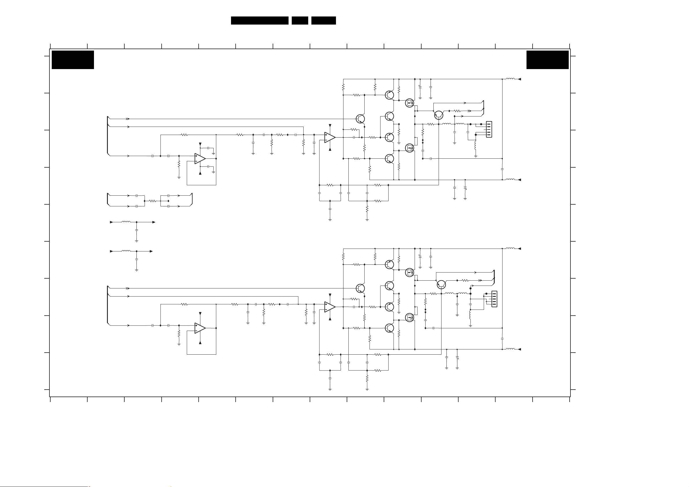
Circuit Diagrams and PWB Layouts
96Q528.1A LA 7.
Audio & AL Supply Panel: Audio
12345678910111213
AP2A AP2A
A
B
C
D
E
F
G
H
I
3104 313 6193.3
1234 13 14
AUDIO: LEFT / RIGHT
MUTE
IN-L
3D29
8K2
+12-15V
7D38-1
LM358P
-12-15V
AUDIO-L
FEEDBACK-L
FEEDBACK-R
MUTE
IN-R
AUDIO-R
5D05
5D06
ID44
2D40
2D24
22n
22n
ID28
3D20
GND-SA
3D19
33K
2D42
22n
2D19
10p
ID02
2D17
10p
VPVP1
VN
2D43
ID30
ID32
22n
3D23
GND-SA
2D16
10p
ID14
2D18
10p
ID27
80R
1u0
2D20
GND-L
ID29
80R
1u0
2D21
GND-L
3D44
8
3
2
4
15K
-12-15V
IN-L
IN-R
8K2
+12-15V
8
5
6
4
15K
-12-15V
ID17
3
5
IDB4
ID19
7
1
ID47
3
5
IDB5
ID49
7
1
25V1m0
2D07
2D06
GND-LL GND-LL
6
7D12
BC857BW
3D17
0R1
4R7
3D18
ID21
ID22
8
1n5
2D08
2D09
1n5
ID23
ID12
2D31
2D32
1m0 25V
GND-LR GND-LR
6
7D37
BC857BW
4R7
3D43
ID51
ID52
8
1n5
2D33
ID53
ID42
3D42
2D34
100n
3D16
2D10
2D12
GND-LL
ID63
GND-LR
2D38
22K
ID48
2D35
5D03
220R
470n
100n
GND-LL
5D08
220R
470n
25V 1m0
GND-LR
FEEDBACK-L
LEFT-SPEAKER
FD27
10n
2D36
FD01
1m025V
2D13
3D41
22K
FD26
FD28
2D41
5D07
CPROT
FD00
5D04
220R
GND-LL
FEEDBACK-R
RIGHT-SPEAKER
10n
220R
GND-LR
ID18
ID62
5D00
ID61
22u
GND-LL
100n
5D25
ID60
0R1
22u
1n5
100n
2D37
GND-LR
7D38-2
LM358P
2DA0
100n
GND-SA
1
2DA1
100n
GND-SA
ID05
3D07
ID16
GND-SA
ID35
3D32
ID46
GND-SA
7D05
BC847BW
ID06
3D08
22K
680R
ID11
3D10
68n
2D05
3D14
560R
7D30
BC847BW
ID36
3D33
22K
680R
ID41
3D35
68n
2D30
560R
3D39
1K2
3D06
7D06
BC807-25W
7D07
BC847BW
ID09
7D08
BC857BW
7D09
BC817-25W
1K2
3D12
100K
3D13
10K
1K2
3D31
7D31
BC807-25W
7D32
BC847BW
ID39
7D33
BC857BW
7D34
BC817-25W
1K2
3D37
100K
3D38
10K
22K
3D69
SI4532ADY
7D10-1
4
ID07
ID08
3D15
330R
GND-LL
ID10
2
7D10-2
SI4532ADY
22K
3D46
ID13
3D70
SI4532ADY
7D35-1
4
ID37
ID38
330R
3D40
GND-LR
ID40
2
7D35-2
SI4532ADY
22K 22K
3D48
ID43
3K3
3D03
3D05
22K
VP
ID01
8
2D03
2D28
680p
680p
7D00-1
3
LM393PT
2
4
VN
3D11
3K9
1n5
ID64
2D44
GND-SA
VP
7D00-2
8
LM393PT
5
6
4
VN
3D36
3K9
1n5
ID65
100n 100n
2D45
GND-SA
2D15
22n
1n0
GND-SA
2D11
ID58
22n
3D22
GND-SA
22K
3D26
ID57
ID20
2D00
3D01
22K
22n
22K
3D21
ID50
2D25
22K
22n
6K8
3D02
GND-SA
3D27
GND-SA GND-SA
2D01
GND-SA
ID31
6K8
2D26
ID15
ID45
ID25
3D71
10K
2DA2
3D72
GND-SA
ID54
10K
1n0
2DA3
GND-SA
ID55
7
ID56
3D24
1M0
ID04
2D02
1
10n
3D09
ID03
22K
ID24
22p
1n5
2D04
2D22
3K3
3D28
3D30
22K
3D25
1M0
ID34
2D27
7
10n
3D34
ID33
22K
ID26
22p
1n5
2D23
2D29
56789101112
1736
B5B-PH-K
CPROT
FD25
1
2
3
4
5
1735
B5B-PH-K-K
5D01
+12-15V
80R
100n
2D14
5D02
-12-15V
80R
5D26
+12-15V
80R
1
2
3
4
5
100n
2D39
5D27
-12-15V
80R
14
H_16801_120.eps
300807
1735 G12
5D27 H13
1736 B12
7D00-1 C8
2D00 C7
7D00-2 G8
2D01 C8
7D05 B9
2D02 C9
7D06 B9
2D03 D8
7D07 B9
2D04 D8
7D08 C9
2D05 D9
7D09 C9
2D06 A10
2D07 A11
2D08 C10
2D09 C11
2D10 C11
2D11 C6
2D12 D11
2D13 D12
2D14 D13
2D15 G6
2D16 D3
2D17 E4
2D18 E3
2D19 D4
2D20 E3
2D21 F3
2D22 D8
2D23 I8
2D24 C3
2D25 G7
2D26 G8
2D27 G9
2D28 I8
2D29 I8
2D30 I9
2D31 F10
2D32 F11
2D33 H10
2D34 H11
2D35 G11
2D36 C12
2D37 I11
2D38 I11
2D39 H13
2D40 C4
2D41 G12
2D42 H3
2D43 H4
2D44 E8
2D45 I8
2DA0 C5
2DA1 C5
2DA2 C6
2DA3 G6
3D01 C7
3D02 C7
3D03 A8
3D05 B9
3D06 A9
3D07 C9
3D08 C9
3D09 C9
3D10 D9
3D11 D8
3D12 D9
3D13 D9
3D14 E9
3D15 C10
3D16 B11
3D17 B11
3D18 C10
3D19 D3
3D20 C4
3D21 C6
3D22 G6
3D23 H4
3D24 B9
3D25 G9
3D26 G6
3D27 G7
3D28 F8
3D29 C4
3D30 F9
3D31 F9
3D32 H9
3D33 G9
3D34 H9
3D35 H9
3D36 I8
3D37 I9
3D38 I9
3D39 I9
3D40 G10
3D41 G12
3D42 G11
3D43 G11
3D44 G4
3D46 C10
3D48 H10
3D69 A10
3D70 F10
3D71 C6
3D72 G5
5D00 B11
5D01 A13
5D02 D13
5D03 B12
5D04 C12
5D05 E3
5D06 F3
5D07 G12
5D08 G12
5D25 G11
5D26 F13
7D10-1 B10
7D10-2 C10
7D12 B11
7D30 G9
7D31 F9
7D32 G9
7D33 G9
7D34 H9
7D35-1 F10
7D35-2 H10
7D37 G11
7D38-1 C4
7D38-2 H5
FD00 B12
FD01 C12
FD25 G12
FD26 G12
FD27 B12
FD28 G12
ID01 C8
ID02 D4
ID03 C8
ID04 C9
ID05 A9
ID06 B9
ID07 B10
ID08 B10
ID09 C9
ID10 C10
ID11 C9
ID12 D10
ID13 D10
ID14 D3
ID15 D8
ID16 D9
ID17 A10
ID18 B11
ID19 B10
ID20 C7
ID21 C11
ID22 C10
ID23 C11
ID24 D8
ID25 C6
ID26 H8
ID27 E3
ID28 C3
ID29 F3
ID30 H3
ID31 G8
ID32 H4
ID33 H8
ID34 G9
ID35 F9
ID36 G9
ID37 F10
ID38 G10
ID39 G9
ID40 H10
ID41 H9
ID42 H10
ID43 I10
ID44 C4
ID45 I8
ID46 I9
ID47 F10
ID48 F11
ID49 G10
ID50 G7
ID51 G11
ID52 G11
ID53 H11
ID54 G6
ID55 C5
ID56 H5
ID57 C6
ID58 G6
ID60 G11
ID61 B11
ID62 B11
ID63 G11
ID64 D8
ID65 I8
IDB4 B10
IDB5 G10
A
B
C
D
E
F
G
H
I
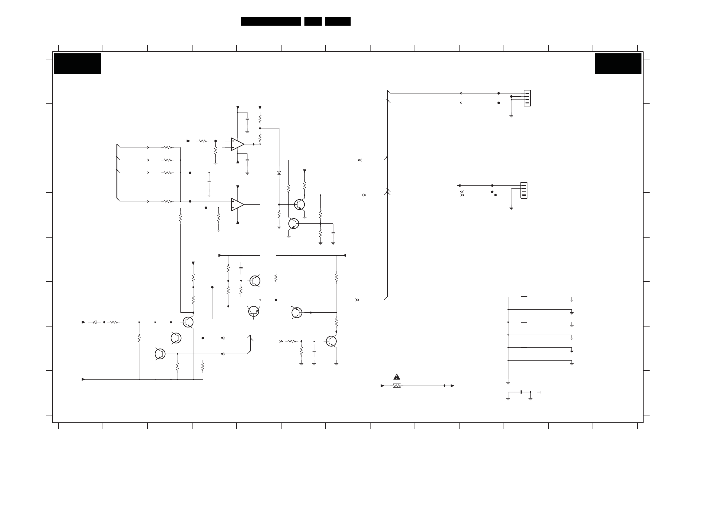
Circuit Diagrams and PWB Layouts
97Q528.1A LA 7.
Audio & AL Supply Panel: Protection
1234567
8 9 10 11 12 13
AUDIO: PROTECTION / MUTE CONTROL
AP2B AP2B
A
B
C
D
G
H
AUDIO-L
MUTE
AUDIO-R
SOUND-ENABLE
AUDIO-PROT
3DD0
10R
+3V3-STANDBY
IDE2
VP1
VP1
+3V3-STANDBY
5K6
100n
2DF2
3DF6
GND-L
2DF3
GND-L
7DF8
100p
BC847BW
100K
3DD3
1
IDF2
100n
7
SOUND-ENABLE
IDE3
22K
SOUND-ENABLE
+3V3-STANDBY
6DF0
BAS316
2K2
3DH1
47K
IDF4
3DG3
3DF9
GND-L
FDG3
3DH0
7DF3
BC847BW
IDF9
2DD4
GND-L
3DG9
3DG8
GND-L
1n5
IDF7
22K
10n
10K
2DD2
GND-L
+12-15V
47K
3DH5
47K
3DG7
IDG0
7DF5
BC847BW
GND-L
47K
GND-L
7DF4
BC847BW
GND-L
47K
BC857BW
7DF6
IDG1
3DG5
47K
47K
3DG6
GND-L
AUDIO-PROT
+12-15V
7DF7-1
LM393PT
3DF8
2K7
IDF8
IDF5
3
2
7DF7-2
LM393PT
5
6
2K7
3DH4
3DH2
8
4
-12-15V
VP1
8
4
-12-15V
33K
2DD7
47K
BC857BW
7DF2
CPROT
CPROT-SW
3DH7
FDH7
47K
FD08
FD14
+12-15V
3DH6
3DG2
7DF1
BC847BW
2K2
47K
IDG7
3DF4
47K
FD09
FDG2
3DG4
2DF0
GND-L
2K2
3DF5
GND-L
1u0
GND-L
-12-15V
FDG4
+12-15V
+SUB-SPEAKER
-SUB-SPEAKER
LEFT-SPEAKER
RIGHT-SPEAKER
3DH3
220K
3DH8
220K
3DF2
220K
3DF3
220K
3DF7
E
F
+12-15V
-12-15V
6DF1
BZX384-C18
IDG6
3DG0
4K7
3DG1
10K
7DH1
BC847BW
IDG5
7DF0
BC847BW
3DH9
2K2
FD04
FD05
FD03
FD02
FD06
FD07
GND+3V3
GND-L
GND-L
GND-SA
B4B-PH-K-K
1738
B4B-PH-K
c006
c002
c001
c003
c005
c004
2DF9
10n
1737
1
2
3
4
1
2
3
4
GND screw
TO
1735 SSB
TO
1738 SSB
GND-LSW
GND-SA
GND-SA
GND-LL
GND-LR
GND+3V3
1
0002
A
B
C
D
G
H
0002 H12
1737 A11
1738 C11
2DD2 D7
2DD4 G6
2DD7 E5
2DF0 C4
2DF2 B5
2DF3 C5
2DF9 H11
3DD0 H8
3DD3 B5
3DF2 C3
3DF3 D3
3DF4 B4
3DF5 C4
3DF6 B5
3DF7 D3
3DF8 D4
3DF9 D5
3DG0 F2
3DG1 G2
3DG2 F3
3DG3 E5
3DG4 G4
3DG5 G6
3DG6 G6
3DG7 F7
3DG8 D6
3DG9 D6
3DH0 C6
3DH1 C6
3DH2 F4
3DH3 B3
3DH4 E4
3DH5 E7
3DH6 E3
3DH7 F5
3DH8 C3
3DH9 G3
6DF0 C5
6DF1 F1
7DF0 G3
7DF1 F4
7DF2 F5
7DF3 D6
7DF4 D6
7DF5 G7
7DF6 F6
7DF7-1 B4
7DF7-2 C4
7DF8 E5
7DH1 G3
FD02 C10
FD03 C10
FD04 A10
E
FD05 A10
FD06 A11
FD07 D10
FD08 C3
FD09 G4
FD14 D3
FDG2 D4
FDG3 F5
FDG4 F4
FDH7 B4
IDE2 H9
F
IDE3 B5
IDF2 B5
IDF4 D5
IDF5 F4
IDF7 D6
IDF8 E4
IDF9 F6
IDG0 G7
IDG1 G6
IDG5 F3
IDG6 F2
IDG7 F4
c001 F11
c002 F11
c003 G11
c004 G11
c005 G11
c006 F11
3104 313 6193.3
12
345678910
H_16801_121.eps
11 12 13
300807

Circuit Diagrams and PWB Layouts
Audio & AL Supply Panel: Subwoofer
1741 B10
2D46 F3
2D47 F10
2D48 F3
2D49 F10
2D50 C2
2D52 C2
2D53 B9
2D54 C5
2D55 C5
2D56 C12
2D57 C13
2D58 D1
2D59 D6
2D60 D2
2D61 D13
2D62 D9
2D63 D10
2D64 D2
2D65 E9
2D66 E8
2D71 D7
2D72 D15
2D73 F6
2D74 F6
2D75 F13
2D76 F13
2D77 F2
2D78 F3
2D79 F4
1234
2D80 F9
2D81 F10
2D82 F11
2D83 D3
2D84 F7
2D86 G7
2D87 F8
2D88 G8
3DK0 C3
3DK1 C4
3DK2 C4
3DK3 C10
3DK4 C11
3DK5 C12
3DK6 C3
3DK7 C11
3DK8 D6
3DK9 D14
98Q528.1A LA 7.
3DL0 D6
3DL1 D13
3DL2 D4
3DL4 D1
3DL5 D12
3DL8 D9
3DL9 D11
3DM0 D2
3DM1 E9
3DM2 E3
3DM4 E11
3DM6 E3
3DM8 E4
3DM9 E12
3DN0 E4
3DN1 E11
3DN2 F3
3DN3 F4
3DN4 F10
3DN5 F11
3DN6 F4
3DN7 F11
3DN8 F4
3DN9 F11
3DP2 D1
3DP3 D8
5D10 B1
5D11 C83DL7 D4
5D12 C15
5D13 C1
5D14 D6
5D15 D13
5D16 E8
5D17 F15
5D18 B9
5D19 B9
7DK0-1 C5
7DK0-2 E5
7DK1-1 D3
7DK1-2 D10
7DK2 C4
7DK3 D5
7DK4 D4
7DK5 D4
7DK6 E4
7DK7 D4
7DL0-1 C12
7DL0-2 E123DM7 E11
7DL1 C11
7DL2 D13
7DL3 D11
7DL4 D11
7DL5 E11
7DL6 E11
FD10 C10
FD11 B9
FD12 B9
FD13 B10
FDM1 B9
FDM2 B9
FDM3 D6
IDK0 B2
IDK1 C5
IDK2 C12
IDK3 C2
IDK4 C4
IDK5 C4
IDK6 D6
IDK7 D5
IDK8 D4
IDK9 D13
IDL0 D5
IDL1 D6
IDL2 D4
IDL3 D2
IDL4 D2
IDL5 D3
IDL6 D4
IDL7 D11
IDL8 E12
IDL9 E4
IDM0 E4
IDM1 E3
IDM2 E10
IDM3 E5
IDM4 F2
IDM5 F4
IDM6 F3
IDM7 D1
IDM8 D6
IDM9 D8
IDN0 C12
IDN1 D13
IDN2 D12
IDN3 E11
IDN4 D12
IDN5 D13
IDN6 D11
IDN7 D9
IDN8 D9
IDN9 D11
IDP0 F11
IDP1 F11
IDP2 D12
IDP3 C11
IDP4 F7
IDP5 F9
IDP6 F3
IDP7 F10
IDP8 F10
IDP9 F3
IDR0 F12
56789101112131415
AP2C AP2C
AUDIO: SUBWOOFER
A
+SUB-SPEAKER
5D18
220R
B
3DP3
10K
GND-SA
IDM9
2D66
2D87
2D88
5D19
220R
IDN7
3DL8
12K
10n
10p
10p
5D10
3DL4
IDK0
80R
2D50
GND-LSW
5D13
IDK3
80R
2D52
GND-LSW
IDL4
2D60
12K
100n
GND-SA
VP1
C
D
MUTE
IN+SW
OUT-L
-12-15V
3DP2
10K
GND-SA
IDM7
2D58
10n
E
F
VP2
1u0
IDK4
3DM2
GND-SA
7DK4
BC847BW
IDL2
3DL7
680R
IDM0
3DN0
2D79
560R
3DN8
1K2
3DK1
7DK2
BC807-25W
7DK7
BC847BW
IDL6
22K
7DK5
BC857BW
7DK6
BC817-25W
1K2
3DN3
IDM5
100K
1u0
3DN6
10K
3K3
VP2
8
4
VN2
3DN2
3K9
IDP9
2D46
GND-SA
7DK1-1
LM393PT
IDM1
100n
2D78
IDP6
3DK0
3DK6
22K
IDL5
2D83
1
10n
3DM6
22K
1n0
22p
2D48
IDM6
VN2
1u0
IDL3
3
2
1n0
6K8
2D64
3DM0
GND-SA
IDM4
1n0
2D77
3DK2
IDK5
IDK8
3DL2
IDL9
3DM8
22K
SI4532ADY
7DK0-1
4
330R
GND-LSW
2
7DK0-2
SI4532ADY
22K
IDK1
IDK7
IDL0
2D54
3
GND-LSW GND-LSW
5
6
7
8
1
IDM3
25V1m0
2D55
7DK3
BC857BW
3DL0
0R1
100n
IDL1
2D73
GND-LSW
IDK6
5D14
22u
100n
GND-LSW
3DK8
22K
IDM8
2D59
GND-LSW
2D74
FDM3
470n
1m025V
FEEDBACK-SW
FEEDBACK+SW
FEEDBACK+SW
CPROT-SW
+SUB-SPEAKER
2D84
10p
2D86
10p
2D71
IDP4
-SUB-SPEAKER
5D11
80R
100n
MUTE
IN-SW
OUT-R
5D16
80R
+12-15V
-12-15V
2D53
2D62
100n
IN-SW
IN+SW
FDM1
10n
FDM2
FD12
IDN8
6K8
2D65
3DM1
GND-SA GND-SA
FD11
IDP5
2D80
1n0
GND-LSW
5
6
1n0
FD13
FD10
VP2
8
4
VN2
3DN4
3K9
IDP8
2D47
GND-SA
7DK1-2
LM393PT
IDM2
100n
2D81
IDP7
1741
1
2
3
4
B4B-EH-A
IDK2
IDP3
3DM4
IDP1
GND-SA
7DL3
BC847BW
IDN6
3DL9
680R
IDN3
3DN1
2D82
3DN9
22K
1u0
560R
1K2
3DK4
3DN5
100K
3DN7
10K
1K2
7DL1
BC807-25W
7DL4
BC847BW
IDL7
7DL5
BC857BW
7DL6
BC817-25W
IDP0
3DK5
IDN0
IDP2
3DL5
IDL8
3DM9
22K
SI4532ADY
7DL0-1
4
GND-LSW
2
7DL0-2
SI4532ADY
22K 330R
3
5
IDN2
IDN4
7
1
2D56
1m0 25V
GND-LSW GND-LSW
6
8
IDR0
2D57
7DL2
BC857BW
3DL1
0R1
100n
GND-LSW
IDN5
2D75
IDN1
5D15
22u
GND-LSW
100n
IDK9
2D61
2D76
3DK9
22K
470n
25V 1m0
GND-LSW
FEEDBACK-SW
CPROT-SW
-SUB-SPEAKER
3K3
3DK3
3DK7
22K
IDN9
2D63
7
10n
3DM7
22K
1n0
22p
2D49
2D72
5D12
80R
100n
5D17
80R
G
+12-15V
-12-15V
A
B
C
D
E
F
G
3104 313 6193.3
12345
678
H_16801_122.eps
300807
9 101112131415
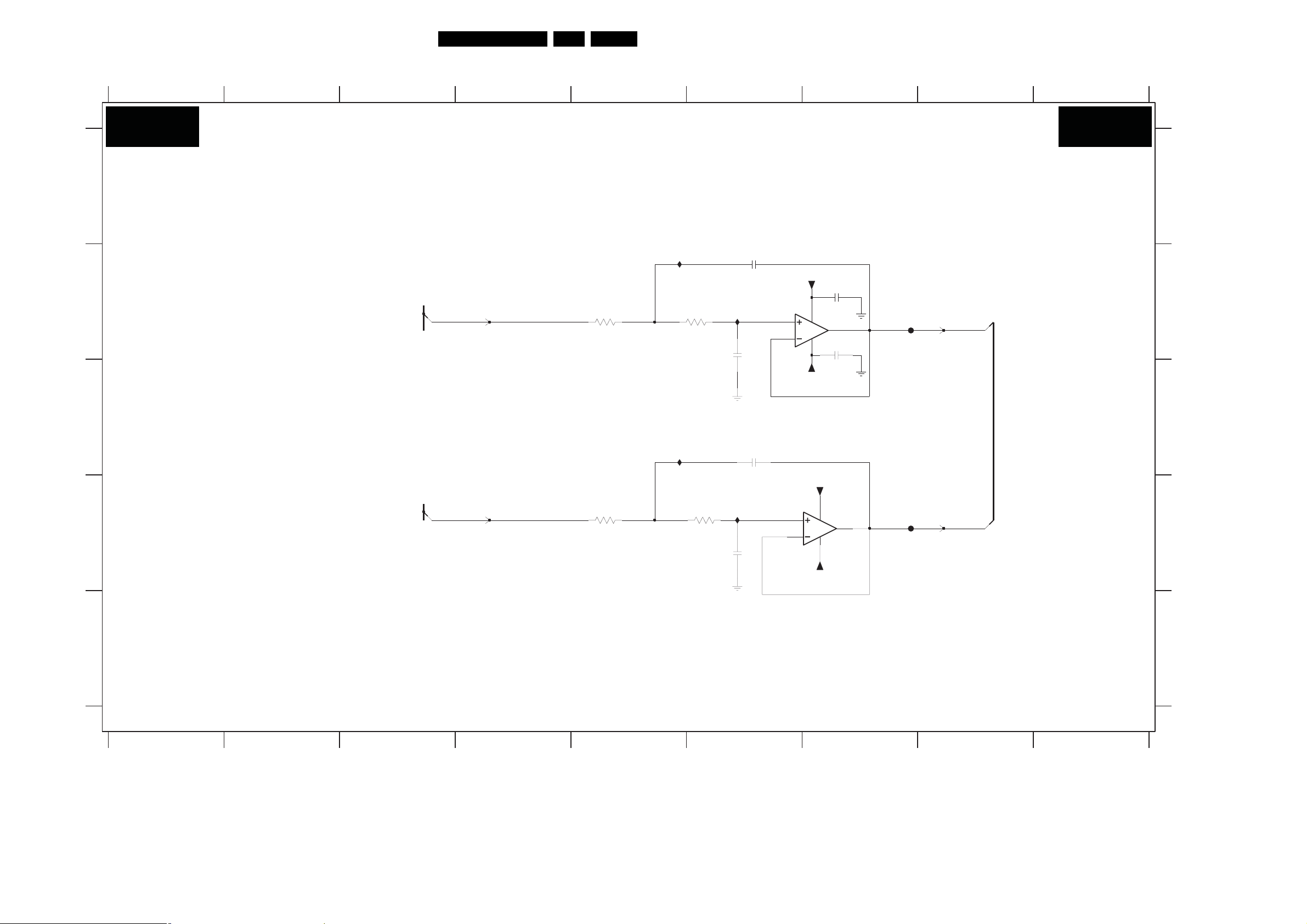
Circuit Diagrams and PWB Layouts
99Q528.1A LA 7.
Audio & AL Supply Panel: Centre Input
123456789
AUDIO: CENTRE INPUT / SW FILTER
AP2D AP2D
A
B
AUDIO-L
3D81
22K
ID87
3D82
22K
ID85
2D95
2D90
4n7
4n7
7D40-1
LM358P
3
2
+12-15V
84
-12-15V
2DC0
100n
1
2DC1
100n
GND-SA
GND-SA
FD84
OUT-L
A
B
2D89 D6
2D90 B6
2D95 B6
2D98 C6
2DC0 B7
2DC1 B7
3D51 D5
3D52 D6
3D81 B5
3D82 B6
7D40-1 B6
7D40-2 D7
FD83 D7
FD84 B7
ID85 B6
ID87 B5
ID89 C5
ID90 D6
C
D
E
3104 313 6193.3
AUDIO-R
3D51
22K
ID89
3D52
22K
GND-SA
ID90
2D89
GND-SA
2D98
4n7
4n7
7D40-2
LM358P
5
6
+12-15V
84
-12-15V
C
7
FD83
OUT-R
D
E
H_16801_123.eps
300807
123456789

Circuit Diagrams and PWB Layouts
Layout Audio & AmbiLight Supply Panel (Top Side)
0002 A9
0P01 C7
0P02 C1
1302 D1
1308 D1
1735 A9
1736 A8
1737 B9
1738 A9
1741 A5
1M18 E4
1M59 E4
1M80 E3
1M81 E3
1P00 C7
1P01 D6
1P03 E1
1P04 C1
1P05 C2
1P06 D9
1P07 C9
1P15 E2
1P16 E3
1P17 E3
1P22 E1
1P30 C6
1P31 E7
2D06 A7
2D13 A7
2D31 A9
2D38 A9
2D54 A7
2D56 B5
2D74 A7
2D76 B5
2P00 B4
2P04 C3
2P05 D3
2P06 C6
2P09 D1
2P10 D2
2P14 C5
2P15 C1
2P16 B3
2P17 B3
2P18 E5
2P19 B1
2P20 D5
2P26 E7
2P27 D9
2P28 C9
2P29 D9
2P30 C9
2P31 E8
2P41 C5
2P47 E7
2P48 E8
2P52 C4
2P54 C4
3D03 A7
3D15 B8
3D28 A9
3D40 A9
3DK0 A6
3DK3 A5
3DL2 A6
3DL5 B5
3P08 C3
3P10 D2
3P12 C1
3P28 C4
3P35 C5
3P36 C5
3P37 C5
3P45 E9
3P51 A4
3P52 A4
3P53 A4
3P54 A3
3P55 A3
3P60 C4
3P77 D3
5D00 A7
5D01 B7
5D02 B7
5D05 B9
5D06 B8
5D10 A6
5D11 B6
5D12 B5
5D13 B6
5D14 A6
5D15 A5
5D16 B6
5D17 B5
5D25 A9
5D26 B9
5D27 A9
5P00 D5
5P01 C5
5P02 A3
5P03 D4
5P04 D5
5P05 D5
5P06 C4
5P07 D4
5P08 C3
5P09 E7
5P10 D7
5P11 C8
5P12 D7
5P13 D7
5P14 D7
5P15 D7
5P16 C2
5P18 C9
5P19 C9
5P20 C9
5P28 E4
5P29 E6
100Q528.1A LA 7.
5P30 E5
5P31 E5
5P32 C2
5P33 C1
5P40 D5
5P41 C5
6P01 D4
6P02 D5
6P05 B3
6P10 E8
6P11 E7
6P12 D7
6P13 D8
7P02 D4
7P11 D4
7P12 D3
9D01 B7
9D02 B7
9D03 B7
9D06 B6
9D07 B8
9D08 B7
9D09 B8
9D10 B7
9D16 B8
9D17 A8
9D18 A8
9D20 B9
9D22 B8
9D23 A8
9D24 B7
9D25 B7
9D26 B9
9D27 B9
9D54 B6
9D55 A8
9D56 A5
9D57 A5
9D58 B6
9D59 B5
9D60 B6
9D61 B7
9D63 B5
9D64 B6
9D65 A5
9D66 A5
9D68 A5
9D70 A7
9D71 A7
9D76 A6
9D77 A6
9D78 B7
9DD5 A9
9DD6 B9
9DD7 B9
9DD8 B9
9DD9 A5
9DE1 B7
9DE2 B9
9DE4 B9
9P02 D2
9P03 B3
9P04 B2
9P05 D2
9P06 B3
9P08 E4
9P09 E5
9P10 E4
9P11 C2
9P12 C1
9P13 E5
9P14 E6
9P22 D4
9P42 D1
9P45 D3
9P47 D4
9P49 D3
9P50 D3
9P51 C7
9P52 C7
9P53 C7
9P54 C7
9P55 D6
9P57 E5
9P58 E6
9P59 D7
9P60 D7
9P61 E8
9P62 E8
9P63 E8
9P64 D8
9P65 D8
9P66 E3
9P67 E4
9P68 E4
9P69 E4
9P70 E5
9P71 E6
9P72 E6
9P73 E6
9P76 D5
9P77 E8
9P78 E8
9P79 D7
9P80 D7
9P81 D8
9P82 D8
9P83 D8
9P84 D8
9P85 D8
9P86 D9
9P87 C7
9P88 C7
9P89 C7
9P90 C7
9P91 C6
9P92 C8
9P93 C8
9P94 C9
9P95 C8
9P96 E7
9P97 E7
9P98 E7
3104 313 6193.3
H_16801_124.eps
310807
 Loading...