

Page 1

Colour Television Chassis
ME8
ME8+
Q528.2E
LA
ME8
Contents Page Contents Page
1. Technical Specifications, Connections, and Chassis
Overview 2
2. Safety Instructions, Warnings, and Notes 6
3. Directions for Use 7
4. Mechanical Instructions 8
5. Service Modes, Error Codes, and Fault Finding 16
6. Block Diagrams, Test Point Overview, and
Waveforms
Wiring Diagram 32" (ME8) 37
Wiring Diagram 42" (ME8) 38
Block Diagram Video 39
Block Diagram Audio 40
Block Diagram Control & Clock Signals 41
SSB: Test Points (Top Side) 42
SSB: Test Points (Bottom Side) 43
I2C IC Overview 44
Supply Lines Overview 45
7. Circuit Diagrams and PWB Layouts Drawing PWB
LCD Supply (37 & 42"): Part 1(A1) 46 48-49
LCD Supply (37 & 42"): Part 2 (A2) 47 48-49
Small Signal Board (B02-B10) 50 98-107
SSB: SRP List Explanation 95
SSB: SRP List Part 1 96
SSB: SRP List Part 2 97
Keyboard Control Panel (E) 108 108
IR & LED Panel (J) 109 110
Light Guide Panel (32") (LG) 111 112
Light Guide Panel (47 & 52") (LG) 113 114
8. Alignments 115
9. IC Data Sheets 123
10. Spare Parts List & CTN Overview 135
11. Revision List 135
ME8+
H_17650_000.eps
160108
©
Copyright 2008 Koninklijke Philips Electronics N.V.
All rights reserved. No part of this publication may be reproduced, stored in a
retrieval system or transmitted, in any form or by any means, electronic,
mechanical, photocopying, or otherwise without the prior permission of Philips.
Published by JY 0866 BU TV Consumer Care Printed in the Netherlands Subject to modification EN 3122 785 17651
Page 2

EN 2 Q528.2E LA1.
Technical Specifications, Connections, and Chassis Overview
1. Technical Specifications, Connections, and Chassis Overview
Index of this chapter:
1.1 Technical Specifications
1.2 Connections
1.3 Chassis Overview
Notes:
• Figures can deviate due to the different set executions.
• Specifications are indicative (subject to change).
1.1 Technical Specifications
1.1.1 Vision
Display type : LCD
Screen size : 32" (82 cm), 16:9
Resolution (H × V pixels) : 1366 × 768p (32")
Light output (cd/m
Contrast ratio : 40000:1 (32")
Viewing angle (H × V degrees) : 176 × 176
Tuning system : PLL
Colour systems : PAL B/G, D/K, I
Video playback : NTSC
Tuner bands : UHF, VHF, S, Hyper
Supported video formats : 480i @ 60 Hz
Supported computer formats:
- 60, 70, 75, 85 Hz : 1024 × 768
- 60, 72, 75, 85 Hz : 800 × 600
- 60, 70, 75, 85 Hz : 640 × 480
2
) : 500 (32")
: 42" (107 cm), 16:9
: 1920 × 1080p (42")
: 550 (42")
: 30000:1 (42")
: SECAM B/G, D/K, L/L’
: DVB-T
: DVB-C (in some sets)
: DVB-T MPEG4
(42PFL5603H/10)
: PAL
: SECAM
: 480p @ 60 Hz
: 576i @ 50 Hz
: 576p @ 50 Hz
: 720p @ 50/60 Hz
: 1080i @ 50/60 Hz
: 1080p @ 24/25/30/
50/60 Hz
1.1.3 Multimedia
Supported file formats : JPEG
USB input : USB2.0
1.1.4 Miscellaneous
Power supply:
- Mains voltage (V
- Mains frequency (Hz) : 50 / 60
Ambient conditions:
- Temperature range (°C) : +5 to +35
Power consumption (values are indicative)
- Normal operation (W) : 140 (32")
- Standby (W) : < 0.15
Dimensions (W × H × D in cm) : 81.9 × 51.8 × 9.5 (32")
Weight (kg) : 19 (32")
) : 220 - 240 ±10%
AC
:MP3
: Slideshow (.alb)
: 200 (42")
: 210
(42PFL7603D/12)
: 104.6 × 64.4 × 8.8
(42")
: 104.6 × 64.4 × 11.1
(42PFL7603D/12)
: 21 (42")
: 22.5
(42PFL7603D/12)
1.1.2 Sound
Maximum power (W
):2× 15
RMS
Page 3
Technical Specifications, Connections, and Chassis Overview
1.2 Connections
EN 3Q528.2E LA 1.
SERV. U
AUDIO OUT
OPTIONAL
L
R
SPDIF
OUT
AUDIO IN
HDMI 2HDMI 3
EXT 3
Y
Pb
Pr
L
R
HDMI 1
EXT 2
(RGB/CVBS)
75X
TV ANTENNA
AUDIO IN :
LEFT / RIGHT
HDMI 1 / DVI
HDMI 2 / DVI
HDMI 3 / DVI
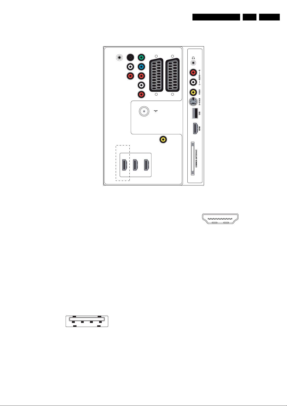
Figure 1-1 Connection overview
EXT 1
(RGB/CVBS)
H_17650_083.eps
160108
Note: The following connector colour abbreviations are used
(acc. to DIN/IEC 757): Bk= Black, Bu= Blue, Gn= Green,
Gy= Grey, Rd= Red, Wh= White, Ye= Yellow.
1.2.1 Side Connections
Headphone (Output)
Bk - Headphone 32 - 600 ohm / 10 mW ot
Cinch: Video CVBS - In, Audio - In
Rd - Audio R 0.5 V
Wh - Audio L 0.5 V
Ye - Video CVBS 1 V
/ 10 kohm jq
RMS
/ 10 kohm jq
RMS
/ 75 ohm jq
PP
S-Video (Hosiden): Video Y/C - In
1 -Ground Y Gnd H
2 -Ground C Gnd H
3 - Video Y 1 V
4 - Video C 0.3 V
/ 75 ohm j
PP
/ 75 ohm j
PP
USB2.0
1 2 3 4
E_06532_022.eps
300904
Figure 1-2 USB (type A)
1-+5V k
2 - Data (-) jk
3 - Data (+) jk
4 - Ground Gnd H
HDMI: Digital Video, Digital Audio - In
19
18 2
1
E_06532_017.eps
250505
Figure 1-3 HDMI (type A) connector
1 - D2+ Data channel j
2 - Shield Gnd H
3 - D2- Data channel j
4 - D1+ Data channel j
5 - Shield Gnd H
6 - D1- Data channel j
7 - D0+ Data channel j
8 - Shield Gnd H
9 - D0- Data channel j
10 - CLK+ Data channel j
11 - Shield Gnd H
12 - CLK- Data channel j
13 - n.c.
14 - n.c.
15 - DDC_SCL DDC clock j
16 - DDC_SDA DDC data jk
17 - Ground Gnd H
18 - +5V j
19 - HPD Hot Plug Detect j
20 - Ground Gnd H
Common Interface
68p - See diagram B09A jk
Page 4
EN 4 Q528.2E LA1.
Technical Specifications, Connections, and Chassis Overview
1.2.2 Rear Connections
Service Connector (UART)
1 - Ground Gnd H
2 - UART_TX Transmit k
3 - UART_RX Receive j
Cinch: S/PDIF - Out
Bk - Coaxial 0.4 - 0.6V
/ 75 ohm kq
PP
Cinch: Audio - Out
Rd - Audio - R 0.5 V
Wh - Audio - L 0.5 V
/ 10 kohm kq
RMS
/ 10 kohm kq
RMS
EXT3: Cinch: Video YPbPr - In
Gn - Video Y 1 V
Bu - Video Pb 0.7 V
Rd - Video Pr 0.7 V
/ 75 ohm jq
PP
/ 75 ohm jq
PP
/ 75 ohm jq
PP
EXT3: Cinch: Audio - In
Rd - Audio - R 0.5 V
Wh - Audio - L 0.5 V
/ 10 kohm jq
RMS
/ 10 kohm jq
RMS
EXT2, EXT1: Video RGB - In, CVBS - In/Out, Audio - In/Out
20
2
3 - D2- Data channel j
4 - D1+ Data channel j
5 - Shield Gnd H
6 - D1- Data channel j
7 - D0+ Data channel j
8 - Shield Gnd H
9 - D0- Data channel j
10 - CLK+ Data channel j
11 - Shield Gnd H
12 - CLK- Data channel j
13 - n.c.
14 - n.c.
15 - DDC_SCL DDC clock j
16 - DDC_SDA DDC data jk
17 - Ground Gnd H
18 - +5V j
19 - HPD Hot Plug Detect j
20 - Ground Gnd H
Mini Jack: HDMI/DVI Audio - In
Rd - Audio - R 0.5 V
Wh - Audio - L 0.5 V
/ 10 kohm jq
RMS
/ 10 kohm jq
RMS
21
E_06532_001.eps
1
050404
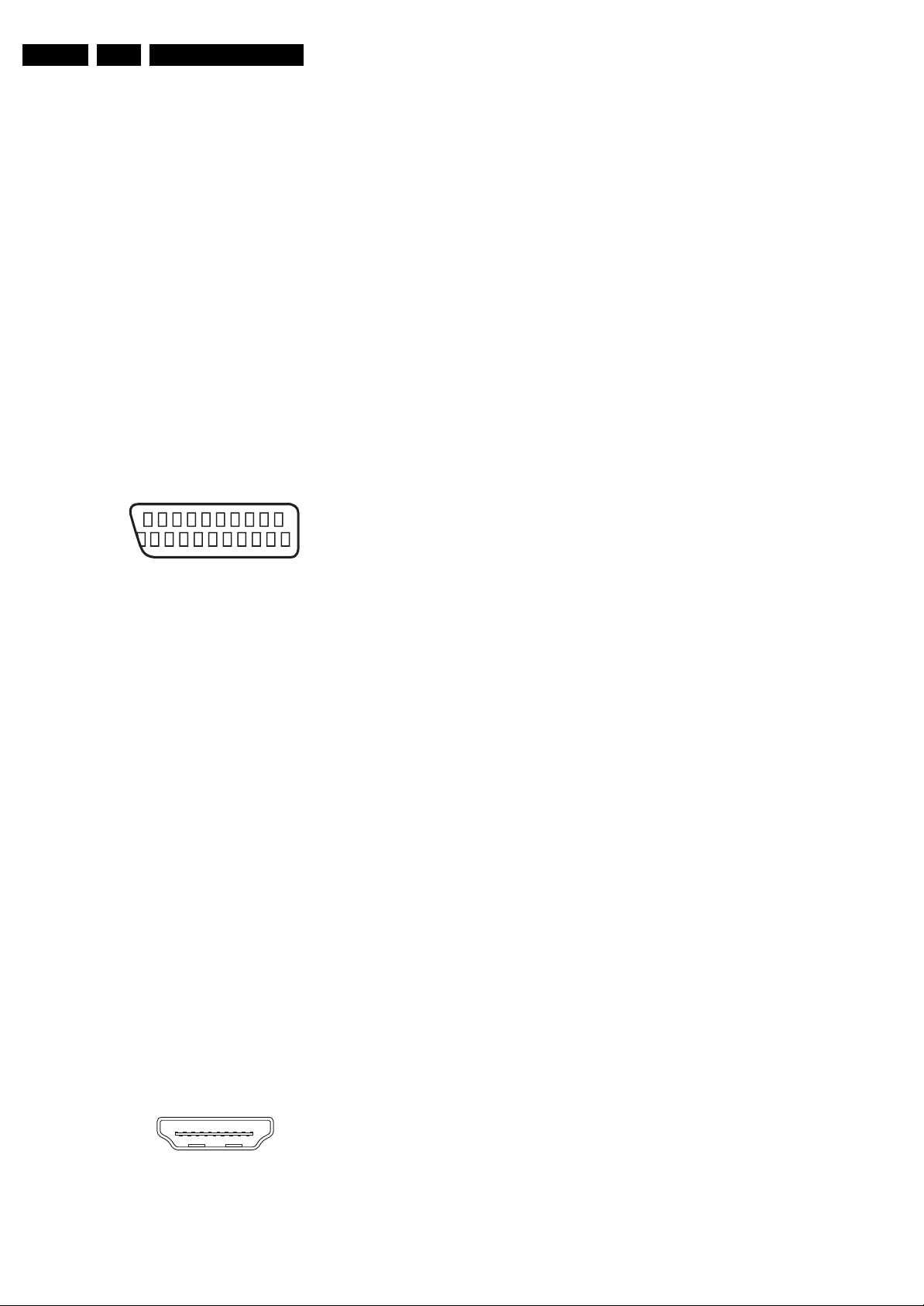
Figure 1-4 SCART connector
1 - Audio R 0.5 V
2 - Audio R 0.5 V
3 - Audio L 0.5 V
4 - Ground Audio Gnd H
/ 1 kohm k
RMS
/ 10 kohm j
RMS
/ 1 kohm k
RMS
5 - Ground Blue Gnd H
6 - Audio L 0.5 V
7 - Video Blue 0.7 V
/ 10 kohm j
RMS
/ 75 ohm jk
PP
8 - Function Select 0 - 2 V: INT
4.5 - 7 V: EXT 16:9
9.5 - 12 V: EXT 4:3 j
9 - Ground Green Gnd H
10 - Easylink P50 0 - 5 V / 4.7 kohm jk
11 - Video Green 0.7 V
/ 75 ohm j
PP
12 - n.c.
13 - Ground Red Gnd H
14 - Ground P50 Gnd H
15 - Video Red 0.7 V
16 - Status/FBL 0 - 0.4 V: INT
/ 75 ohm j
PP
1 - 3 V: EXT / 75 ohm j
17 - Ground Video Gnd H
18 - Ground FBL Gnd H
19 - Video CVBS 1 V
20 - Video CVBS 1 V
/ 75 ohm k
PP
/ 75 ohm j
PP
21 - Shield Gnd H
Aerial - In
- - IEC-type (EU) Coax, 75 ohm D
HDMI 1, 2 (& 3: optional): Digital Video, Digital Audio - In
19
18 2
1
E_06532_017.eps
250505
Figure 1-5 HDMI (type A) connector
1 - D2+ Data channel j
2 - Shield Gnd H
Page 5
Technical Specifications, Connections, and Chassis Overview
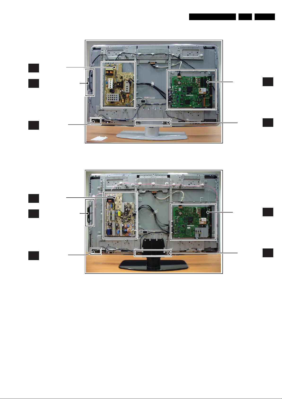
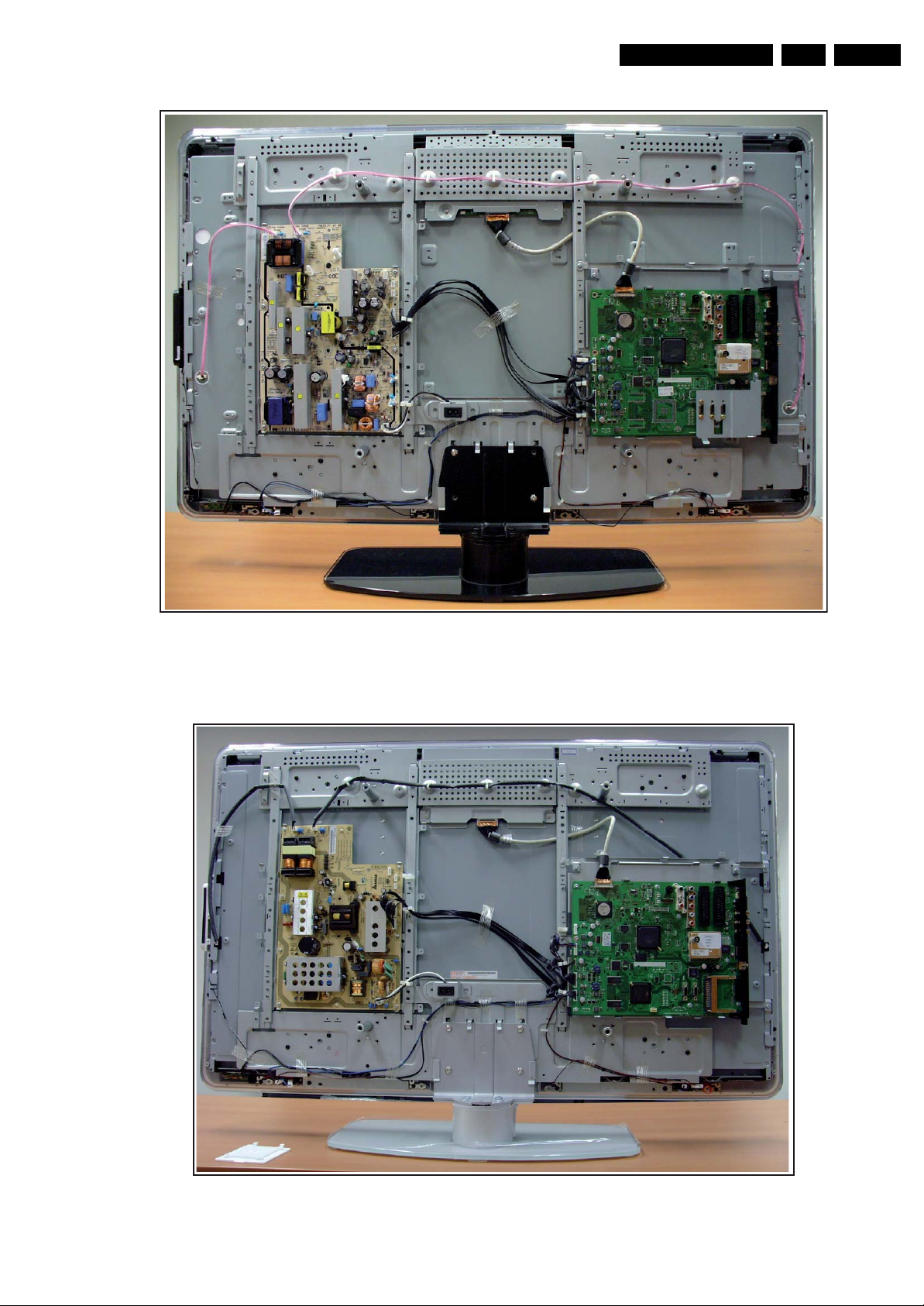
1.3 Chassis Overview
MAIN
A
SUPPLY PANEL
EN 5Q528.2E LA 1.
KEYBOARD CONTROL
E
PA NE L
IR & LED PANEL
J
MAIN
A
SUPPLY PANEL
KEYBOARD CONTROL
E
PA NE L
H_17650_083.eps
Figure 1-6 PWB/CBA locations sets with AmbiLight
160108
SMALL SIGNAL
BOARD
LIGHT GUIDE
PA NE L
H_17650_086.eps
SMALL SIGNAL
BOARD
B
LG
230508
B
IR & LED PANEL
J
H_17650_083.eps
Figure 1-7 PWB/CBA locations sets without AmbiLight
160108
LIGHT GUIDE
PA NE L
H_17650_084.eps
LG
230508
Page 6

EN 6 Q528.2E LA2.
Safety Instructions, Warnings, and Notes
2. Safety Instructions, Warnings, and Notes
Index of this chapter:
2.1 Safety Instructions
2.2 Warnings
2.3 Notes
2.1 Safety Instructions
Safety regulations require the following during a repair:
• Connect the set to the Mains/AC Power via an isolation
transformer (> 800 VA).
• Replace safety components, indicated by the symbol h,
only by components identical to the original ones. Any
other component substitution (other than original type) may
increase risk of fire or electrical shock hazard.
Safety regulations require that after a repair, the set must be
returned in its original condition. Pay in particular attention to
the following points:
• Route the wire trees correctly and fix them with the
mounted cable clamps.
• Check the insulation of the Mains/AC Power lead for
external damage.
• Check the strain relief of the Mains/AC Power cord for
proper function.
• Check the electrical DC resistance between the Mains/AC
Power plug and the secondary side (only for sets that have
a Mains/AC Power isolated power supply):
1. Unplug the Mains/AC Power cord and connect a wire
between the two pins of the Mains/AC Power plug.
2. Set the Mains/AC Power switch to the “on” position
(keep the Mains/AC Power cord unplugged!).
3. Measure the resistance value between the pins of the
Mains/AC Power plug and the metal shielding of the
tuner or the aerial connection on the set. The reading
should be between 4.5 MΩ and 12 MΩ.
4. Switch “off” the set, and remove the wire between the
two pins of the Mains/AC Power plug.
• Check the cabinet for defects, to prevent touching of any
inner parts by the customer.
2.2 Warnings
• All ICs and many other semiconductors are susceptible to
electrostatic discharges (ESD w). Careless handling
during repair can reduce life drastically. Make sure that,
during repair, you are connected with the same potential as
the mass of the set by a wristband with resistance. Keep
components and tools also at this same potential.
• Be careful during measurements in the high voltage
section.
• Never replace modules or other components while the unit
is switched “on”.
• When you align the set, use plastic rather than metal tools.
This will prevent any short circuits and the danger of a
circuit becoming unstable.
2.3 Notes
2.3.1 General
• Measure the voltages and waveforms with regard to the
chassis (= tuner) ground (H), or hot ground (I), depending
on the tested area of circuitry. The voltages and waveforms
shown in the diagrams are indicative. Measure them in the
Service Default Mode (see chapter 5) with a colour bar
signal and stereo sound (L: 3 kHz, R: 1 kHz unless stated
otherwise) and picture carrier at 475.25 MHz for PAL, or
61.25 MHz for NTSC (channel 3).
• Where necessary, measure the waveforms and voltages
with (D) and without (E) aerial signal. Measure the
voltages in the power supply section both in normal
operation (G) and in stand-by (F). These values are
indicated by means of the appropriate symbols.
2.3.2 Schematic Notes
• All resistor values are in ohms, and the value multiplier is
often used to indicate the decimal point location (e.g. 2K2
indicates 2.2 kΩ).
• Resistor values with no multiplier may be indicated with
either an “E” or an “R” (e.g. 220E or 220R indicates 220 Ω).
• All capacitor values are given in micro-farads (μ=× 10
nano-farads (n =× 10
• Capacitor values may also use the value multiplier as the
decimal point indication (e.g. 2p2 indicates 2.2 pF).
• An “asterisk” (*) indicates component usage varies. Refer
to the diversity tables for the correct values.
• The correct component values are listed in the Spare Parts
List. Therefore, always check this list when there is any
doubt.
2.3.3 BGA (Ball Grid Array) ICs
Introduction
For more information on how to handle BGA devices, visit this
URL: www.atyourservice.ce.philips.com (needs subscription,
not available for all regions). After login, select “Magazine”,
then go to “Repair downloads”. Here you will find Information
on how to deal with BGA-ICs.
BGA Temperature Profiles
For BGA-ICs, you must use the correct temperature-profile,
which is coupled to the 12NC. For an overview of these profiles,
visit the website www.atyourservice.ce.philips.com (needs
subscription, but is not available for all regions)
You will find this and more technical information within the
“Magazine”, chapter “Repair downloads”.
For additional questions please contact your local repair help
desk.
2.3.4 Lead-free Soldering
Due to lead-free technology some rules have to be respected
by the workshop during a repair:
• Use only lead-free soldering tin Philips SAC305 with order
code 0622 149 00106. If lead-free solder paste is required,
please contact the manufacturer of your soldering
equipment. In general, use of solder paste within
workshops should be avoided because paste is not easy to
store and to handle.
• Use only adequate solder tools applicable for lead-free
soldering tin. The solder tool must be able:
– To reach a solder-tip temperature of at least 400°C.
– To stabilize the adjusted temperature at the solder-tip.
– To exchange solder-tips for different applications.
• Adjust your solder tool so that a temperature of around
360°C - 380°C is reached and stabilized at the solder joint.
Heating time of the solder-joint should not exceed ~ 4 sec.
Avoid temperatures above 400°C, otherwise wear-out of
tips will increase drastically and flux-fluid will be destroyed.
To avoid wear-out of tips, switch “off” unused equipment or
reduce heat.
• Mix of lead-free soldering tin/parts with leaded soldering
tin/parts is possible but PHILIPS recommends strongly to
avoid mixed regimes. If this cannot be avoided, carefully
clear the solder-joint from old tin and re-solder with new tin.
-9
), or pico-farads (p =× 10
-12
-6
),
).
Page 7

2.3.5 Alternative BOM identification
Note: on European Service website, “Alternative BOM” is
referred to as “Design variant”.
The third digit in the serial number (example:
AG2B0335000001) indicates the number of the alternative
B.O.M. (Bill Of Materials) that has been used for producing the
specific TV set. In general, it is possible that the same TV
model on the market is produced with e.g. two different types
of displays, coming from two different suppliers. This will then
result in sets which have the same CTN (Commercial Type
Number; e.g. 28PW9515/12) but which have a different B.O.M.
number.
By looking at the third digit of the serial number, one can
identify which B.O.M. is used for the TV set he is working with.
If the third digit of the serial number contains the number “1”
(example: AG1B033500001), then the TV set has been
manufactured according to B.O.M. number 1. If the third digit is
a “2” (example: AG2B0335000001), then the set has been
produced according to B.O.M. no. 2. This is important for
ordering the correct spare parts!
For the third digit, the numbers 1...9 and the characters A...Z
can be used, so in total: 9 plus 26= 35 different B.O.M.s can be
indicated by the third digit of the serial number.
Identification: The bottom line of a type plate gives a 14-digit
serial number. Digits 1 and 2 refer to the production centre (e.g.
AG is Bruges), digit 3 refers to the B.O.M. code, digit 4 refers
to the Service version change code, digits 5 and 6 refer to the
production year, and digits 7 and 8 refer to production week (in
example below it is 2006 week 17). The 6 last digits contain the
serial number.
Directions for Use
MODEL :
PROD.NO:
32PF9968/10
AG 1A0617 000001
220-240V 50/60Hz
VHF+S+H+UHF
S
Figure 2-1 Serial number (example)
2.3.6 Board Level Repair (BLR) or Component Level Repair
(CLR)
If a board is defective, consult your repair procedure to decide
if the board has to be exchanged or if it should be repaired on
component level.
If your repair procedure says the board should be exchanged
completely, do not solder on the defective board. Otherwise, it
cannot be returned to the O.E.M. supplier for back charging!
2.3.7 Practical Service Precautions
• It makes sense to avoid exposure to electrical shock.
While some sources are expected to have a possible
dangerous impact, others of quite high potential are of
limited current and are sometimes held in less regard.
• Always respect voltages. While some may not be
dangerous in themselves, they can cause unexpected
reactions that are best avoided. Before reaching into a
powered TV set, it is best to test the high voltage insulation.
It is easy to do, and is a good service precaution.
EN 7Q528.2E LA 3.
MADE IN BELGIUM
~
128W
BJ3.0E LA
E_06532_024.eps
260308
3. Directions for Use
You can download this information from the following websites:
http://www.philips.com/support
http://www.p4c.philips.com
Page 8
EN 8 Q528.2E LA4.
Mechanical Instructions
4. Mechanical Instructions
Index of this chapter:
4.1 Cable Dressing
4.2 Service Positions
4.3 Assy/Panel Removal ME8(+) Styling
4.4 Set Re-assembly
4.1 Cable Dressing
Notes:
• Figures below can deviate slightly from the actual situation,
due to the different set executions.
Figure 4-1 Cable dressing 32" sets without AmbiLight
I_17651_001.eps
110608
Page 9
Mechanical Instructions
EN 9Q528.2E LA 4.
Figure 4-2 Cable dressing 42" sets with AmbiLight
H_17650_085.eps
170108
Figure 4-3 Cable dressing 42" sets without AmbiLight
H_17650_087.eps
160108
Page 10
EN 10 Q528.2E LA4.
Mechanical Instructions
4.2 Service Positions
For easy servicing of this set, there are a few possibilities
created:
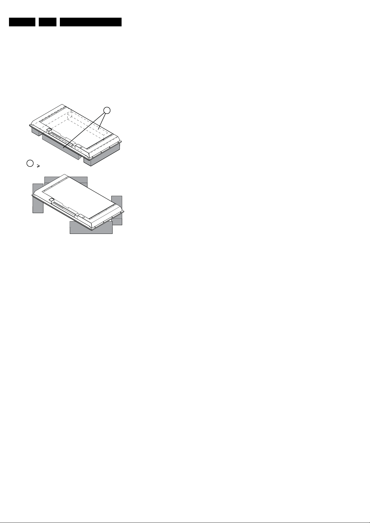
• The buffers from the packaging (see figure “Rear cover”).
• Foam bars (created for Service).
• Aluminium service stands (created for Service).
4.2.1 Foam Bars
1
Required for sets
1
42"
3. Remove the screws [2], gently lift the back cover from the
set and unplug the Ambilight power connector [4].
4. Lift the back cover from the TV. Make sure that wires and
flat coils are not damaged while lifting the rear cover from
the set.
E_06532_018.eps
171106
Figure 4-4 Foam bars
The foam bars (order code 3122 785 90580 for two pieces) can
be used for all types and sizes of Flat TVs. See figure “Foam
bars” for details. Sets with a display of 42" and larger, require
four foam bars [1]. Ensure that the foam bars are always
supporting the cabinet and never only the display.
Caution: Failure to follow these guidelines can seriously
damage the display!
By laying the TV face down on the (ESD protective) foam bars,
a stable situation is created to perform measurements and
alignments. By placing a mirror under the TV, you can monitor
the screen.
4.3 Assy/Panel Removal ME8(+) Styling
4.3.1 Rear Cover
Warning: Disconnect the mains power cord before you remove
the rear cover.
Note: it is not necessary to remove the stand while removing
the rear cover.
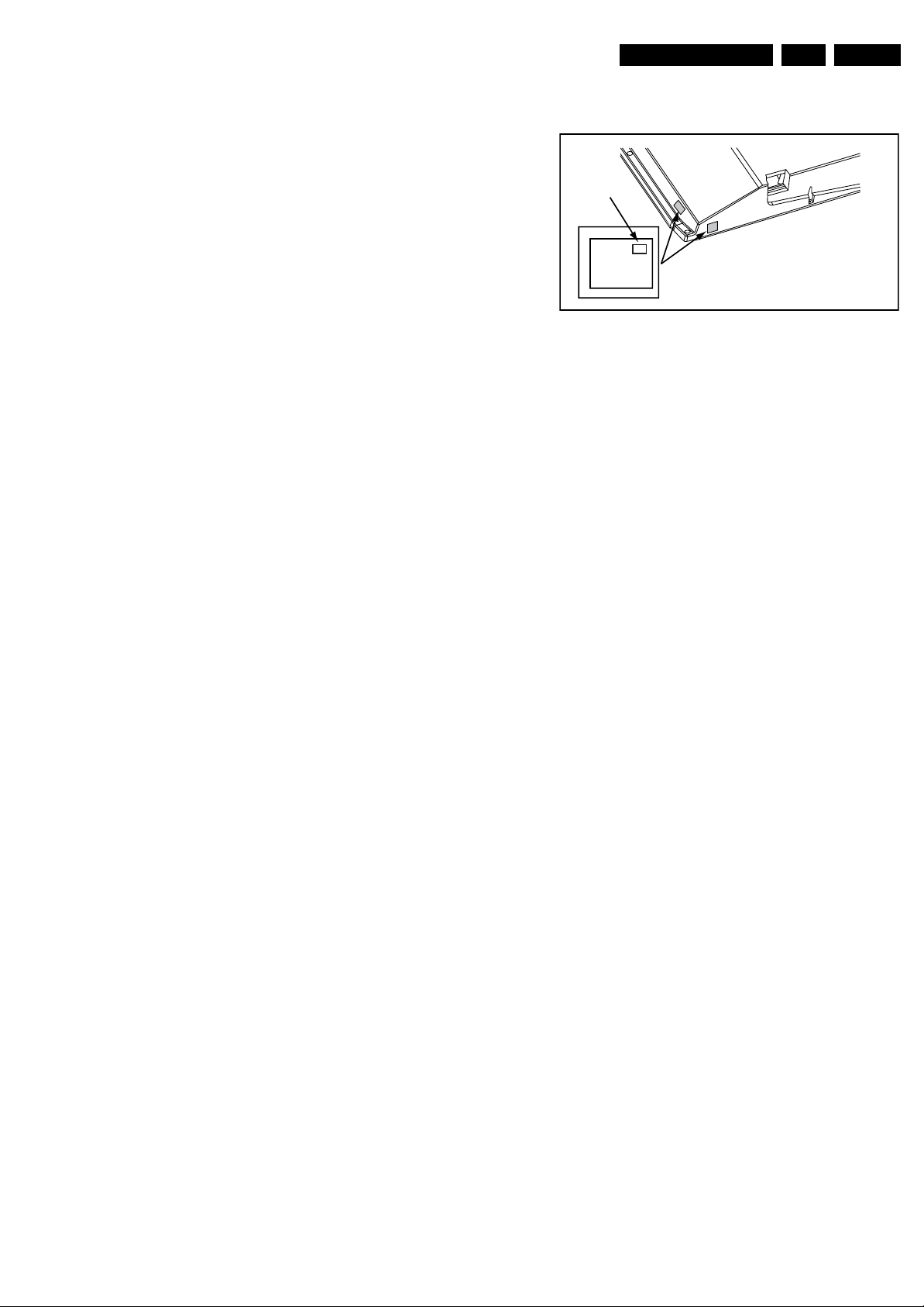
Warning: Most sets have an additional hatch located in the
rear cover. These are meant for disconnecting the flat cables to
the AmbiLight units in the rear cover, before the rear cover is
lifted from the set. The hatches are not always located at the
same place for all sets, therefore the figures below are only
meant as indication.
It is mandatory to locate these hatches first, open them, and
unplug connectors behind. Lifting the back cover without
having done so, could result in damaging the connectors
inside!
Refer to next figures for details.
1. First remove the screws [1] from the back cover hatch and
remove the hatch.
2. Then unplug connector [3].
Page 11
Mechanical Instructions
EN 11Q528.2E LA 4.
2
2 2
222
H_17650_100.eps
2
2
2
2
2
180108
2
2
2
2
2
2
2 2
1
1
2
2
2
Figure 4-5 Back Cover Removal [1/3]
Figure 4-6 Back Cover Removal [2/3]
3
H_17650_099.eps
180108
4
Figure 4-7 Back Cover Removal [3/3]
H_17650_101.eps
180108
Page 12
EN 12 Q528.2E LA4.
4.3.2 Ambilight
Mechanical Instructions
Refer to next figure for details.
1. Unplug the connectors [1].
2. Remove the screws [2].
3. Pull the unit sidewards from the back cover.
When defective, replace the whole unit.
2
1
H_17650_097.eps
180108
1
2
Figure 4-10 Tweeter
4.3.5 IR & LED Board
Refer to next figure for details.
1. Unplug connectors [1].
2. Use a flat screw driver to release the clip by pushing it in
the indicated direction [2].
3. Lift the board and take it out of the set.
When defective, replace the whole unit.
1
H_17650_095.eps
180108
Figure 4-8 Ambilight Unit
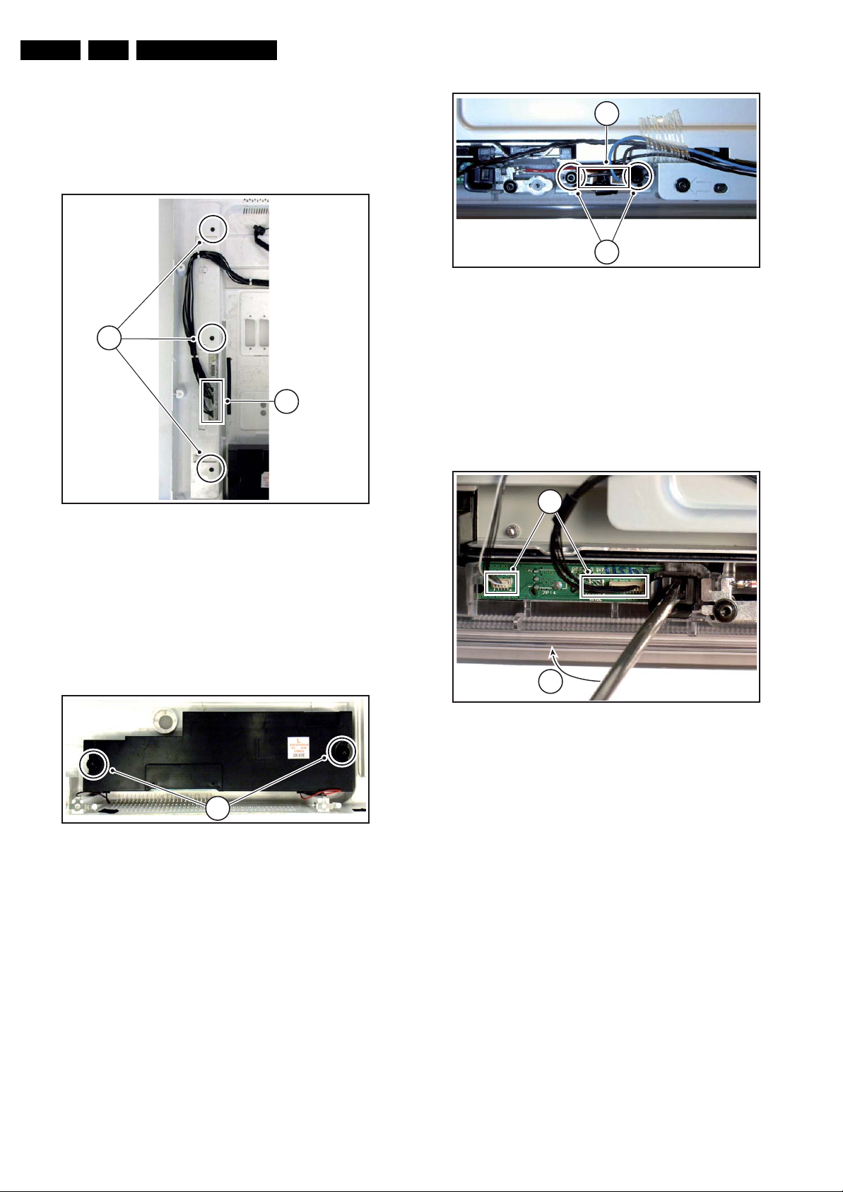
4.3.3 Woofers
Refer to next figure for details.
1. Remove the screws [1] and lift the whole unit from the back
cover.
Take the speakers out together with their casing. When
defective, replace the whole unit.
1
Figure 4-9 Woofer
4.3.4 Tweeters
Refer to next figure for details.
Warning: The speakers should never be connected or
disconnected when the set is playing! This can damage the
amplifiers on the SSB.
1. Remove the screws [1] lift the whole unit from the back
cover.
When defective, replace the whole unit.
H_17650_096.eps
180108
2
Figure 4-11 IR & LED Board
H_17650_098.eps
180108
Page 13
Mechanical Instructions
EN 13Q528.2E LA 4.
4.3.6 Key Board
Refer to next figure for details.
1. Unplug the key board connector from the IR & LED board.
2. Remove the screws [1].
3. Lift the unit and take it out of the set.
When defective, replace the whole unit.
1
Figure 4-12 Key Board
H_17650_094.eps
180108
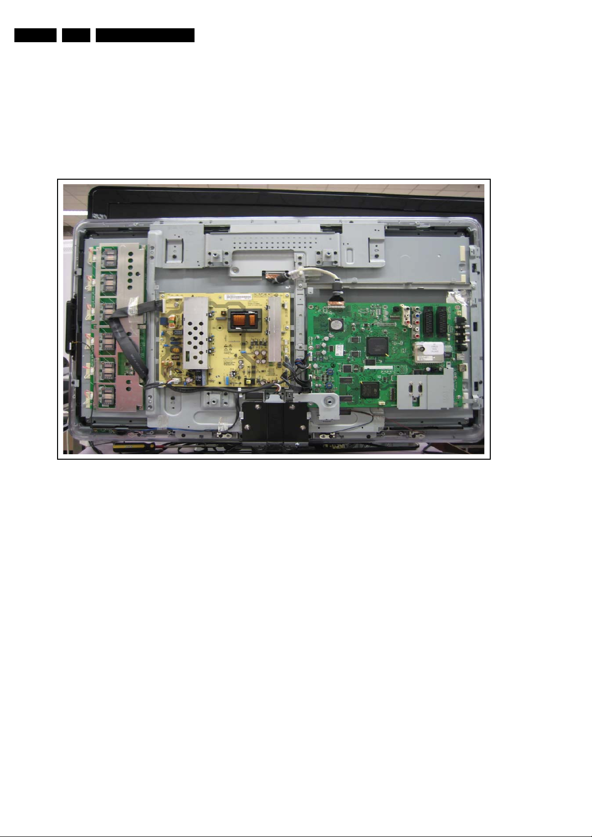
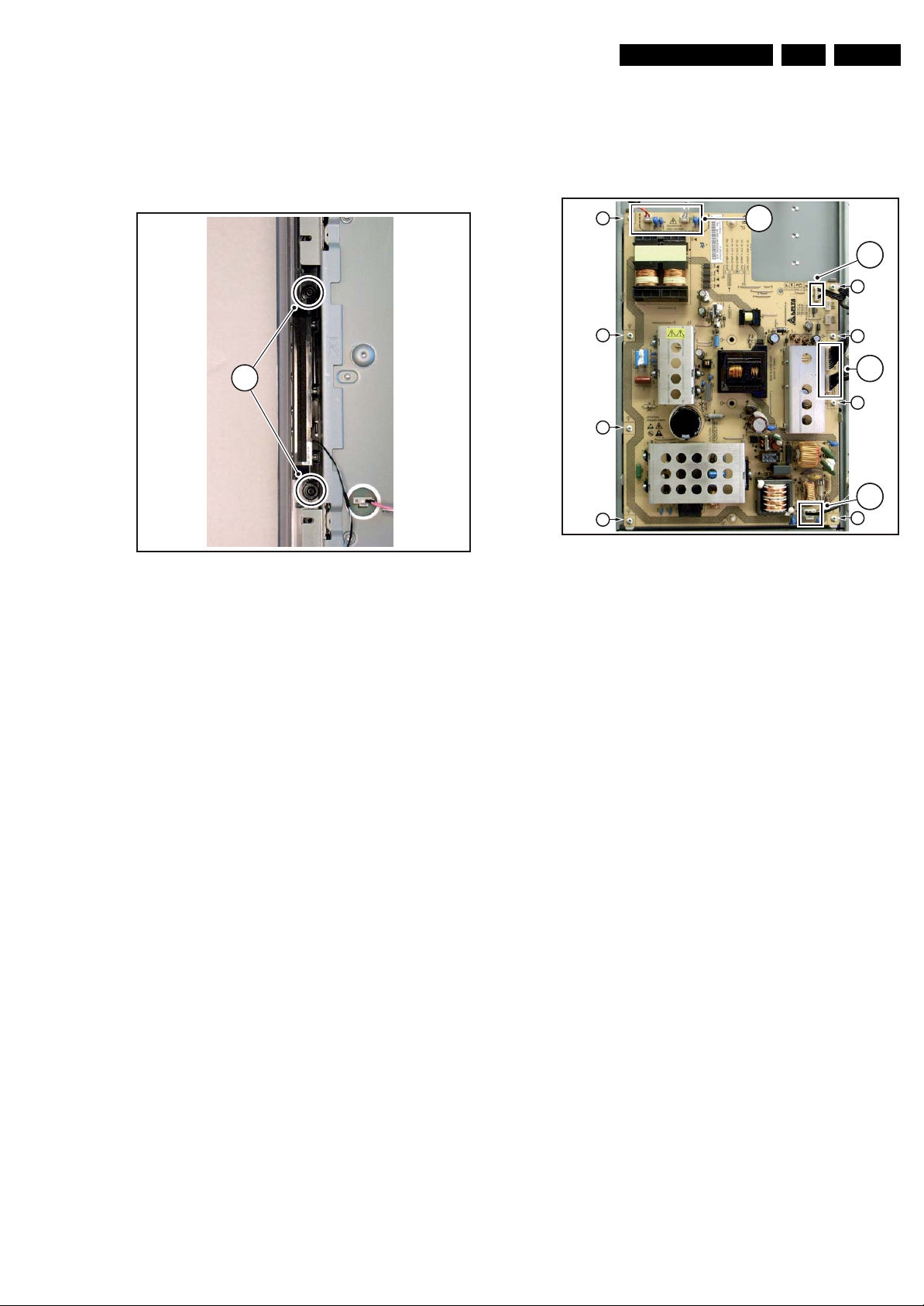
4.3.7 Display Supply Panel
Refer to next figure for details.
1. Unplug connectors [1].
2. Remove the fixation screws [2].
3. Take the board out.
2
2
2
2
Figure 4-13 Display Supply Panel
1
1
2
2
1
2
1
2
H_17650_102.eps
180108
Page 14
EN 14 Q528.2E LA4.
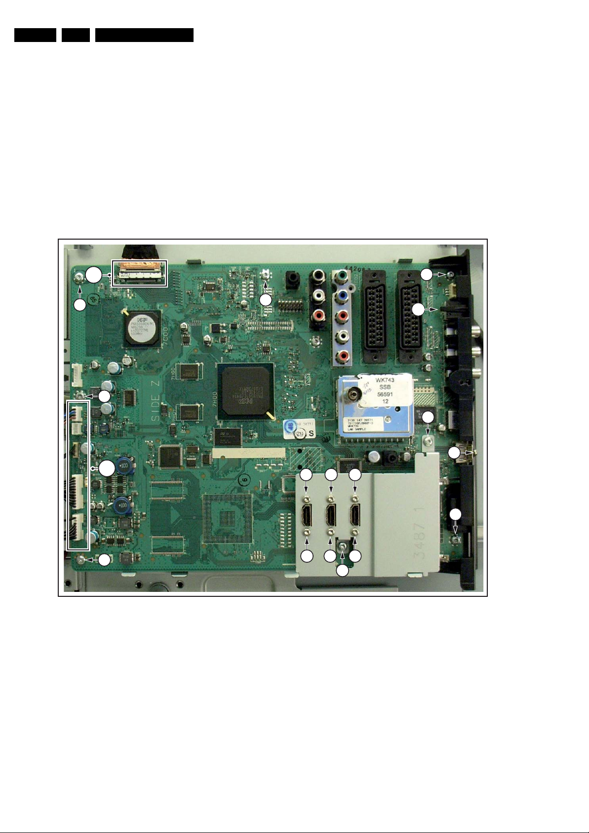
4.3.8 Small Signal Board (SSB)
Refer to next figure for details.
Caution: it is mandatory to remount all different screws at their
original position during re-assembly. Failure to do so may result
in damaging the SSB.
Refer to next figures or details.
1. Unplug the LVDS connector [1].
Caution: be careful, as this is a very fragile connector!
2. Unplug the connectors [2].
3. Remove the screws [3].
4. The SSB can now be taken out of the set, together with the
front shield and the side cover.
5. To remove the shield, remove the screws [4] and lift it of.
6. To remove the side cover remove the screws [5].
7. Release clip [6] and slide the pull the cover sidewards from
the SSB.
Mechanical Instructions
1
3
3
3
6
3
3
5
2
4 4 4
3
3
4 4 4
3
Figure 4-14 Small Signal Board
H_17650_103.eps
180108
Page 15
4.3.9 LCD Panel / Lightguide
Refer to next figures for details.
1. Unplug the LVDS connector [1].
Caution: be careful, as this is a very fragile connector!
2. Unplug the connectors [2].
3. Remove the fixation screws [3] from rim.
4. Take the rim from the set.
5. Remove the fixation screws [4] and [5].
6. Lift the subframe from the set.
7. The LCD panel can now be lifted from the front cabinet.
When the Lightguide is defective the entire front cabinet has to
be removed. To do so follow the previous steps to remove the
LCD panel as well as removing the IR LED panel and
Tweeters.
Mechanical Instructions
EN 15Q528.2E LA 4.
4
5
5
4
5
4
5
3
1
22
3
5
5
4 4
5
5
4
44
2
H_17650_104.eps
180108
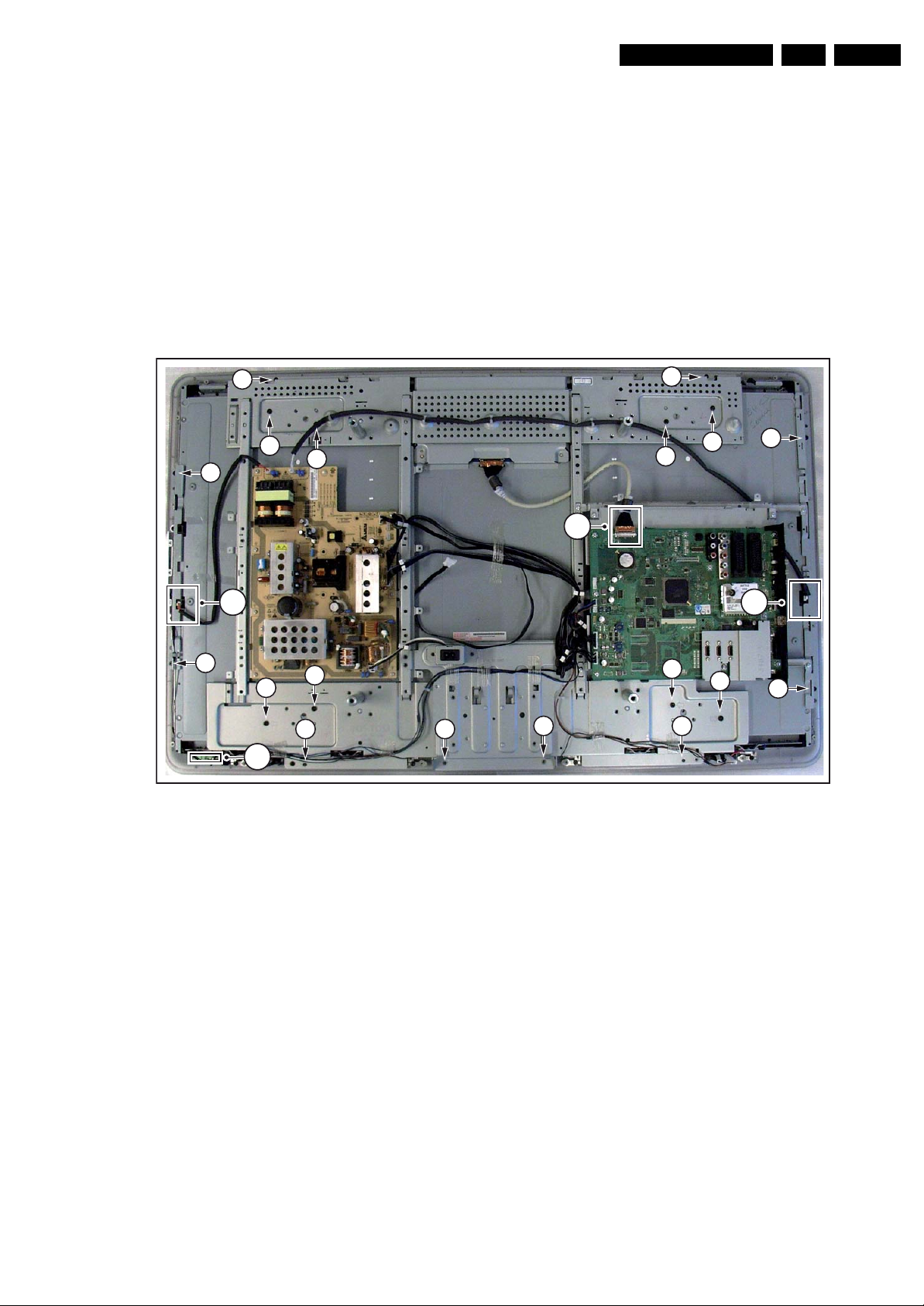
4.4 Set Re-assembly
To re-assemble the whole set, execute all processes in reverse
order.
Notes:
• While re-assembling, make sure that all cables are placed
and connected in their original position. See figure “Cable
dressing”.
• Pay special attention not to damage the EMC foams on the
SSB shields. Ensure that EMC foams are mounted
correctly.
Figure 4-15 LCD Panel / Lightguide
Page 16
EN 16 Q528.2E LA5.
Service Modes, Error Codes, and Fault Finding
5. Service Modes, Error Codes, and Fault Finding
Index of this chapter:
5.1 Test Points
5.2 Service Modes
5.3 Stepwise Start-up
5.4 Service Tools
5.5 Error Codes
5.6 The Blinking LED Procedure
5.7 Protections
5.8 Fault Finding and Repair Tips
5.9 Software Upgrading
5.1 Test Points
As most signals are digital, it will be difficult to measure
waveforms with a standard oscilloscope. However, several key
ICs are capable of generating test patterns, which can be
controlled via ComPair. In this way it is possible to determine
which part is defective.
Perform measurements under the following conditions:
• Service Default Mode.
• Video: Colour bar signal.
• Audio: 3 kHz left, 1 kHz right.
5.2 Service Modes
Service Default mode (SDM) and Service Alignment Mode
(SAM) offers several features for the service technician, while
the Customer Service Mode (CSM) is used for communication
between the call centre and the customer.
This chassis also offers the option of using ComPair, a
hardware interface between a computer and the TV chassis. It
offers the abilities of structured troubleshooting, error code
reading, and software version read-out for all chassis.
(see also paragraph “ComPair”).
– Picture mute (blue mute or black mute).
– Automatic volume levelling (AVL).
– Skip/blank of non-favourite pre-sets.
How to Activate SDM
For this chassis there are two kinds of SDM: an analogue SDM
and a digital SDM. Tuning will happen according table “SDM
Default Settings”.
• Analogue SDM: use the standard RC-transmitter and key
in the code “062596”, directly followed by the “MENU”
button.
Note: It is possible that, together with the SDM, the main
menu will appear. To switch it “off”, push the “MENU”
button again.
• Digital SDM: use the standard RC-transmitter and key in
the code “062593”, directly followed by the “MENU” button.
Note: It is possible that, together with the SDM, the main
menu will appear. To switch it “off”, push the “MENU”
button again.
• Analogue SDM can also be activated by shorting for a
moment the two solder pads [1] (see figure “Service mode
pads”) on the SSB, with the indication “SDM”. Activation
can be performed in all modes, except when the set has a
problem with the Stand-by Processor.
SDMSDM
5.2.1 Service Default Mode (SDM)
Purpose
• To create a pre-defined setting, to get the same
measurement results as given in this manual.
• To override SW protections detected by stand-by
processor and make the TV start up to the step just before
protection (a sort of automatic stepwise start up). See
paragraph “Stepwise Start Up”.
• To override SW protections detected by MIPS. See also
paragraph “Error codes”.
• To start the blinking LED procedure (not valid for
protections detected by standby software).
Specifications
Table 5-1 SDM default settings
Region Freq. (MHz)
Europe, AP(PAL/Multi) 475.25 PAL B/G
Europe, AP DVB-T 546.00 PID
Video: 0B 06 PID
PCR: 0B 06 PID
Audio: 0B 07
• All picture settings at 50% (brightness, colour, contrast).
• All sound settings at 50%, except volume at 25%.
• All service-unfriendly modes (if present) are disabled, like:
– (Sleep) timer.
– Child/parental lock.
Default
system
DVB-T
Figure 5-1 Service mode pads
After activating this mode, “SDM” will appear in the upper right
corner of the screen (if you have picture).
How to Navigate
When you press the “MENU” button on the RC transmitter, the
set will toggle between the SDM and the normal user menu
(with the SDM mode still active in the background).
How to Exit SDM
Use one of the following methods:
• Switch the set to STAND-BY via the RC-transmitter.
• Via a standard customer RC-transmitter: key in “00”sequence.
5.2.2 Service Alignment Mode (SAM)
Purpose
• To perform (software) alignments.
• To change option settings.
• To easily identify the used software version.
• To view operation hours.
• To display (or clear) the error code buffer.
H_17650_088.eps
160108
Page 17
Service Modes, Error Codes, and Fault Finding
EN 17Q528.2E LA 5.
How to Activate SAM
Via a standard RC transmitter: key in the code “062596”
directly followed by the “INFO” button. After activating SAM
with this method a service warning will appear on the screen,
you can continue by pressing the red button on the RC.
Contents of SAM:
• Hardware Info.
– A. SW Version. Displays the software version of the
main software (example: Q582E-1.2.3.4 =
AAAAB_X.Y.W.Z).
• AAAA= the chassis name.
• B= the region: A= AP, E= EU, L= LatAm, U = US.
For AP sets it is possible that the Europe software
version is used.
• X.Y.W.Z= the software version, where X is the
main version number (different numbers are not
compatible with one another) and Y.W.Z is the sub
version number (a higher number is always
compatible with a lower number).
– B. SBY PROC Version. Displays the software version
of the stand-by processor.
– C. Production Code. Displays the production code of
the TV, this is the serial number as printed on the back
of the TV set. Note that if an NVM is replaced or is
initialized after corruption, this production code has to
be re-written to NVM. ComPair will foresee in a
possibility to do this.
• Operation Hours. Displays the accumulated total of
operation hours (not the stand-by hours). Every time the
TV is switched “on/off”, 0.5 hours is added to this number.
• Errors (followed by maximal 10 errors). The most recent
error is displayed at the upper left (for an error explanation
see paragraph “Error Codes”).
• Reset Error Buffer. When you press “cursor right” (or the
“OK button) and then the “OK” button, the error buffer is
reset.
• Alignments. This will activate the “ALIGNMENTS” submenu.
• Dealer Options. Extra features for the dealers.
• Options. Extra features for Service. For more info
regarding option codes, see chapter 8 “Alignments”.
Note that if you change the option code numbers, you have
to confirm your changes with the “OK” button before you
store the options. Otherwise you will loose your changes.
• Initialize NVM. The moment the processor recognizes a
corrupted NVM, the “initialize NVM” line will be highlighted.
Now, you can do two things (dependent of the service
instructions at that moment):
– Save the content of the NVM via ComPair for
development analysis, before initializing. This will give
the Service department an extra possibility for
diagnosis (e.g. when Development asks for this).
– Initialize the NVM.
Note: When you have a corrupted NVM, or you have replaced
the NVM, there is a high possibility that you will not have picture
anymore because your display code is not correct. So, before
you can initialize your NVM via the SAM, you need to have a
picture and therefore you need the correct display option. Refer
to chapter 8 for details. To adapt this option, you can use
ComPair (the correct HEX values for the options can be found
in chapter 8 “Alignments”) or a method via a standard RC
(described below).
Changing the display option via a standard RC: Key in the
code “062598” directly followed by the “MENU” button and
“XXX”, where XXX is the 3 digit decimal display code (see table
“Option code overview” in chapter 8 “Alignments”, or sticker on
the side/bottom of the cabinet). Make sure to key in all three
digits, also the leading zero’s. If the above action is successful,
the front LED will go out as an indication that the RC sequence
was correct. After the display option is changed in the NVM, the
TV will go to the Stand-by mode. If the NVM was corrupted or
empty before this action, it will be initialized first (loaded with
default values). This initializing can take up to 20 seconds.
Display Option
Code
39mm
040
PHILIPS
MODEL:
32PF9968/10
27mm
PROD.SERIAL NO:
AG 1A0620 000001
(CTN Sticker)
E_06532_038.eps
240108
Figure 5-2 Location of Display Option Code sticker
• Store. All options and alignments are stored when
pressing “cursor right” (or the “OK” button) and then the
“OK”-button.
• SW Maintenance.
– SW Events. Not useful for Service purposes. In case
of specific software problems, the development
department can ask for this info.
– HW Events. Not useful for Service purposes. In case
of specific software problems, the development
department can ask for this info.
• Test settings. For development purposes only.
• Upload to USB. To upload several settings from the TV to
a USB stick, which is connected to the Side I/O. The items
are “Channel list”, “Personal settings”, “Option codes”,
“Display-related alignments” and “History list”. First you
have to create a directory “repair” in the root of the USB
stick.To upload the settings you have to select each item
separately, press “cursor right” (or the “OK button), confirm
with “OK” and wait until “Done” appears. In case the
download to the USB stick was not successful “Failure” will
appear. In this case, check if the USB stick is connected
properly and if the directory “repair” is present in the root of
the USB stick. Now the settings are stored onto your USB
stick and can be used to download onto another TV or
other SSB. Uploading is of course only possible if the
software is running and if you have a picture. This method
is created to be able to save the customer’s TV settings
and to store them into another SSB.
• Download from USB. To download several settings from
the USB stick to the TV. Same way of working as with
uploading. To make sure that the download of the channel
list from USB to the TV is executed properly, it is necessary
to restart the TV and tune to a valid preset if necessary.
Note: The “History list item” can not be downloaded from
USB to the TV. This is a “read-only” item. In case of specific
problems, the development department can ask for this
info.
How to Navigate
• In SAM, you can select the menu items with the “CURSOR
UP/DOWN” key on the RC-transmitter. The selected item
will be highlighted. When not all menu items fit on the
screen, move the “CURSOR UP/DOWN” key to display the
next/previous menu items.
• With the “CURSOR LEFT/RIGHT” keys, it is possible to:
– (De) activate the selected menu item.
– (De) activate the selected sub menu.
• With the “OK” key, it is possible to activate the selected
action.
How to Exit SAM
Use one of the following methods:
• Press the “MENU” button on the RC-transmitter.
• Switch the set to STAND-BY via the RC-transmitter.
Page 18

EN 18 Q528.2E LA5.
Service Modes, Error Codes, and Fault Finding
5.2.3 Customer Service Mode (CSM)
Purpose
When a customer is having problems with his TV-set, he can
call his dealer or the Customer Helpdesk. The service
technician can then ask the customer to activate the CSM, in
order to identify the status of the set. Now, the service
technician can judge the severity of the complaint. In many
cases, he can advise the customer how to solve the problem,
or he can decide if it is necessary to visit the customer.
The CSM is a read only mode; therefore, modifications in this
mode are not possible.
When in this chassis CSM is activated, a colour bar test pattern
will be visible for 5 seconds. This test pattern is generated by
the Pacific3. So if you see this test pattern you can determine
that the back end video chain (Pacific3, LVDS, and display) of
the SSB is working. In case of a set with DFI panel, an extra
test picture is generated. So you will see the Pacific3 test
picture for 3 seconds and then the DFI EPLD test picture for
another 3 seconds. With this extra test picture you can
determine if the DFI board is working properly.
Also new in this chassis: when you activate CSM and there is
a USB stick connected to the TV, the software will dump the
complete CSM content to the USB stick. The file (Csm.txt) will
be saved in the root of your USB stick. This info can be handy
if you do not have picture.
Another new item in this chassis is when CSM is activated, the
complete error-buffer content will be shown via the blinking
LED procedure.
How to Activate CSM
Key in the code “123654” via the standard RC transmitter.
Note: Activation of the CSM is only possible if there is no (user)
menu on the screen!
How to Navigate
By means of the “CURSOR-DOWN/UP” knob on the RCtransmitter, you can navigate through the menus.
Contents of CSM
• Set Type. This information is very helpful for a helpdesk/
workshop as reference for further diagnosis. In this way, it
is not necessary for the customer to look at the rear of the
TV-set. Note that if an NVM is replaced or is initialized after
corruption, this set type has to be re-written to NVM.
ComPair will foresee in a possibility to do this.
• Production Code. Displays the production code (the serial
number) of the TV. Note that if an NVM is replaced or is
initialized after corruption, this production code has to be
re-written to NVM. ComPair will foresee a in possibility to
do this.
• Code 1. Gives the last five errors of the error buffer. As
soon as the built-in diagnose software has detected an
error, the buffer is adapted. The last occurred error is
displayed on the leftmost position. Each error code is
displayed as a 2-digit number. When less than 10 errors
occur, the rest of the buffer is empty (00). See also
paragraph “Error Codes” for a description.
• Code 2. Gives the first five errors of the error buffer. See
also paragraph “Error Codes” for a description.
• Options 1. Gives the option codes of option group 1 as set
in SAM (Service Alignment Mode).
• Options 2. Gives the option codes of option group 2 as set
in SAM (Service Alignment Mode).
• 12NC SSB. Gives an identification of the SSB as stored in
NVM. Note that if an NVM is replaced or is initialized after
corruption, this identification number has to be re-written to
NVM. ComPair will foresee in a possibility to do this. This
identification number consists of 14 characters and is built
up as follows:
- Seven last characters of the 12NC of the SSB itself.
- the serial number of the SSB, which consists of seven
digits. Both can be found on a sticker on the PWB of the
SSB itself. The format of the identification number is then
as follows: <last seven characters of 12NC of SSB><serial
number of SSB> (total fourteen characters).
• Installed date. Indicates the date of the first installation of
the TV. This date is acquired via time extraction.
• Digital Natural Motion. Gives the status of the Digital
Natural Motion setting as set by the customer. Remark: a
customer can choose between “OFF”, “MINIMUM” and
“MAXIMUM”, but in CSM this item will only show “OFF” or
“ON” (“ON” in case the customer has choosen “MINIMUM”
or “MAXIMUM”)
• Pixel Plus. Gives the last status of the Perfect Pixel HD
setting, as set by the customer. Possible values are “ON”
and “OFF”. See DFU on how to change this item.
• DNR. Gives the last status of the Noise reduction setting,
as set by the customer. Possible values are “OFF”,
“MINIMUM”, “MEDIUM” and “MAXIMUM”. See DFU on
how to change this item.
• Noise Figure. Gives an indication of the signal quality for
the selected transmitter. Possible values are “BAD”,
“AVERAGE”, “GOOD“ and “DIGITAL”. In case of a digital
channel, this item will never indicate: “BAD”, “GOOD” or
“AVERAGE” but only displays “DIGITAL”.
• 12NC Display. Shows the 12NC of the display.
• Headphone Volume. Gives the last status of the
headphone volume, as set by the customer. The value can
vary from 0 (volume is minimum) to 100 (volume is
maximum). See DFU on how to change this item.
• Surround Mode. Indicates the by the customer selected
sound mode (or automatically chosen mode). Possible
values are “STEREO” and “VIRTUAL DOLBY
SURROUND”. It can also have been selected
automatically by signalling bits (internal software). See
DFU on how to change this item.
• AVL. Indicates the last status of AVL (Automatic Volume
Level) as set by the customer: See DFU on how to change
this item.
• Delta Volume. Indicates the last status of the delta volume
for the selected preset as set by the customer: from “-12”
to “+12”. See DFU on how to change this item.
• Volume. Indicates the last status of the volume for the
selected preset as set by the customer: from “0” to “100”.
See DFU on how to change this item.
• Balance. Indicates the last status of the balance for the
selected preset as set by the customer: from “-10” to “+10”.
See DFU on how to change this item.
• Preset Lock. Indicates if the selected preset has a child
lock: “LOCKED” or “UNLOCKED”. See DFU on how to
change this item.
• Lock after. Indicates at what time the channel lock is set:
“OFF” or e.g. “18:45” (lock time). See DFU on how to
change this item.
• Parental rating lock. Indicates the “Parental rating” as set
by the customer. See DFU on how to change this item.
• Parental rating status. Indicates the “Parental rating” as
transmitted by the broadcaster (if applicable). If the
parental rating status is indicating a higher age then the
parental rating lock as set by the customer, you will need to
enter the child lock code.
• TV ratings lock. Only applicable for US.
• Movie ratings lock. Only applicable for US.
• On timer. Indicates if the “On timer” is set “ON” or “OFF”
and when it is set to “ON”, also start time, start day and
program number is displayed. See DFU on how to change
this item.
• Location. Gives the last status of the location setting as
set via the installation menu. Possible values are “SHOP”
and “HOME”. If the location is set to “SHOP”, several
settings are fixed. So for a customer location must be set
to “HOME”. Can be changed via the installation menu (see
also DFU).
• HDMI key validity. Indicates if the HDMI keys (or HDCP
keys) are valid or not. In case these keys are not valid and
Page 19

Service Modes, Error Codes, and Fault Finding
the customer wants to make use of the HDMI functionality,
the SSB has to be replaced.
• Tuner frequency. Indicates the frequency the transmitter
is tuned to.
• TV System. Gives information about the video system of
the selected transmitter. In case a DVBT signal is received
this item will also show ATSC.
– BG: PAL BG signal received
– DK: PAL DK signal received
– L/La: SECAM L/La signal received
– I: PAL I signal received
– M: NTSC M signal received
– ATSC: ATSC signal received
– DVB: DVBT signal received
• 12NC one zip SW. Displays the 12NC number of the onezip file as it is used for programming software in production.
In this one-zip file all below software versions can be found.
• Initial main SW. Displays the main software version which
was initially loaded by the factory.
• Current main SW. Displays the built-in main software
version. In case of field problems related to software,
software can be upgraded. As this software is consumer
upgradeable, it will also be published on the Internet.
Example: Q582E_1.2.3.4.
• Flash utils SW. Displays the software version of the
software which contains all necessary components of the
download application. To program this software, EJTAG
tooling is needed. Example: Q582E_1.2.3.4.
• Standby SW. Displays the built-in stand-by processor
software version. Upgrading this software will be possible
via ComPair or via USB (see chapter Software upgrade).
Example: STDBY_3.0.1.2.
• MOP SW. Only applicable for US. At the time of release of
this manual, there was still a problem with this item, and
some rubbisch was displayed. Ignore this.
• Pacific 3 Flash SW. Displays the Pacific 3 software
version.
• NVM version. Displays the NVM version as programmed
by factory.
• Display parameters. for development purposes only.
• Private PQ parameters. for development purposes only.
• Public PQ parameters. for development purposes only.
• Ambilight parameters. for development purposes only.
• Acoustics parameters. for development purposes only.
• DFI software (if applicable). Displays the DFI EPLD
software.
• DFI ambilight software (if applicable). Displays the DFI
ambilight EPLD software.
EN 19Q528.2E LA 5.
How to Exit CSM
Press “MENU” on the RC-transmitter.
Page 20
EN 20 Q528.2E LA5.
Service Modes, Error Codes, and Fault Finding
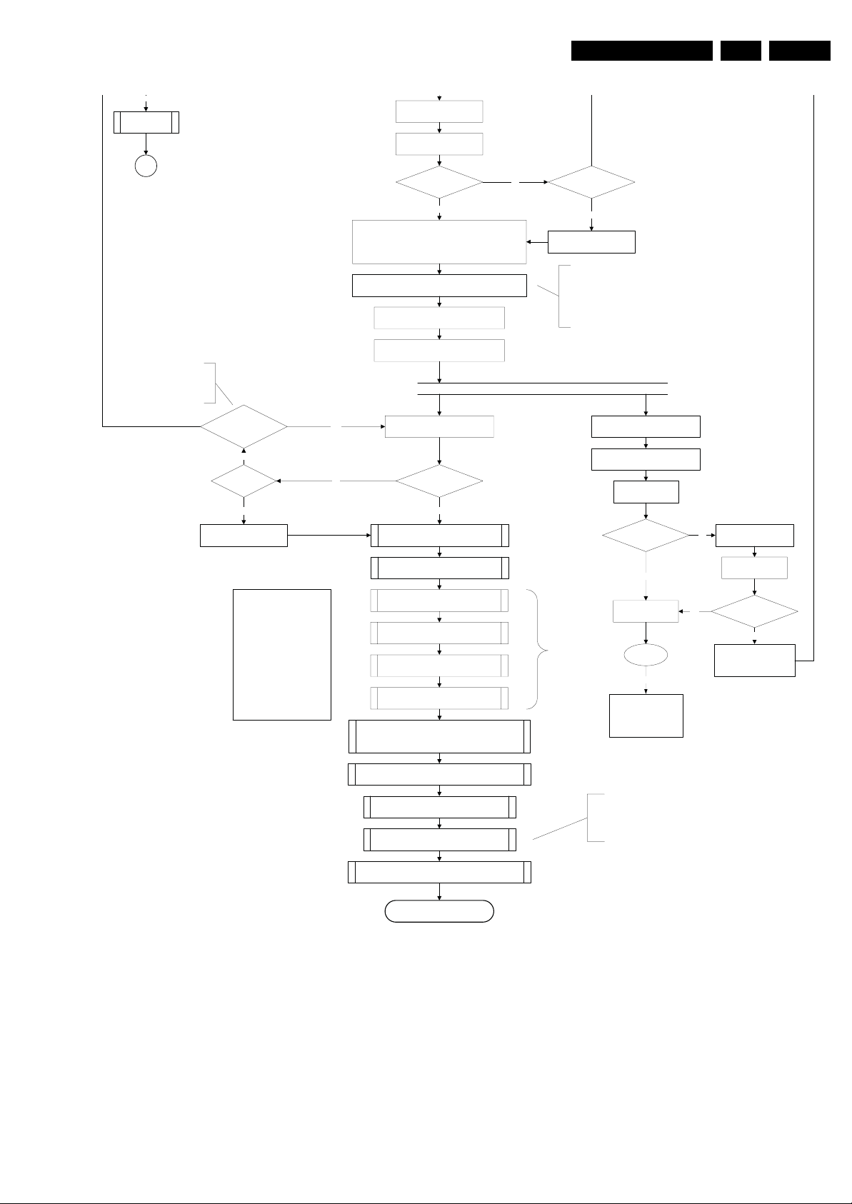
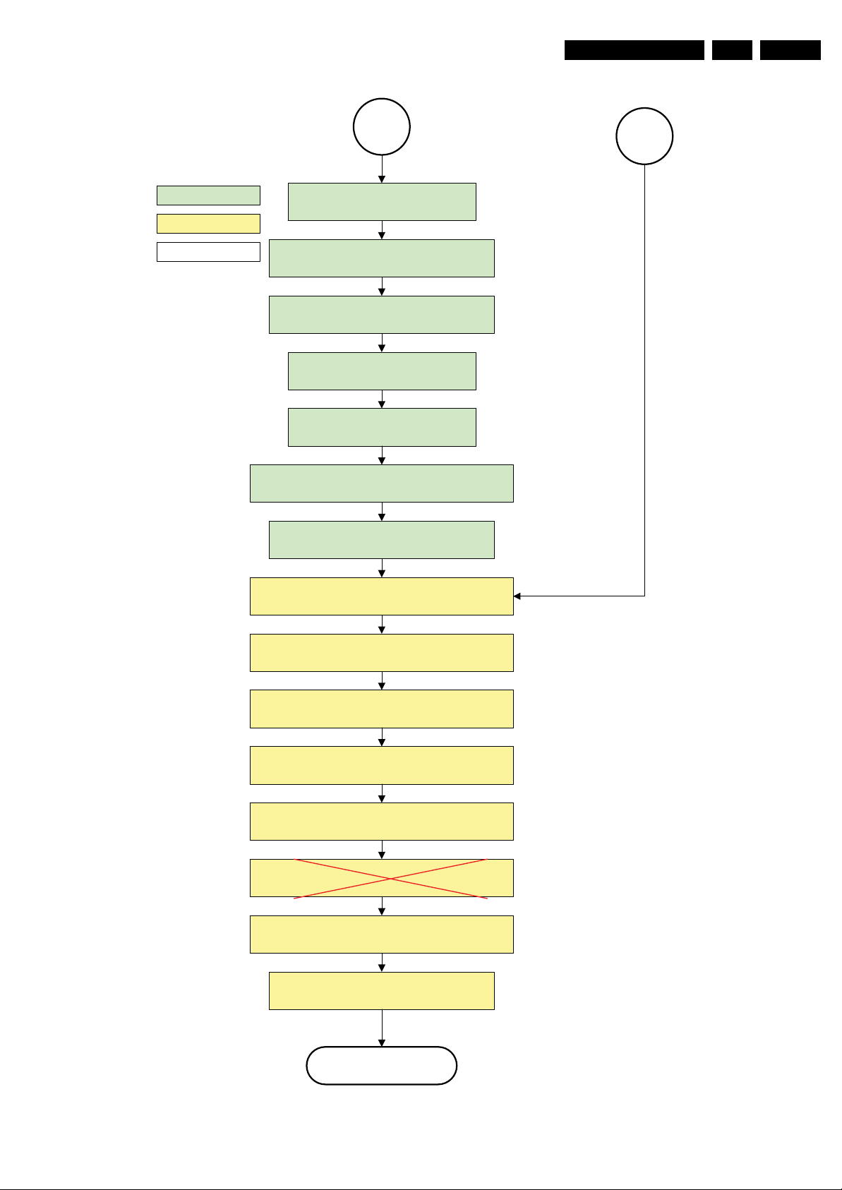
5.3 Stepwise Start-up
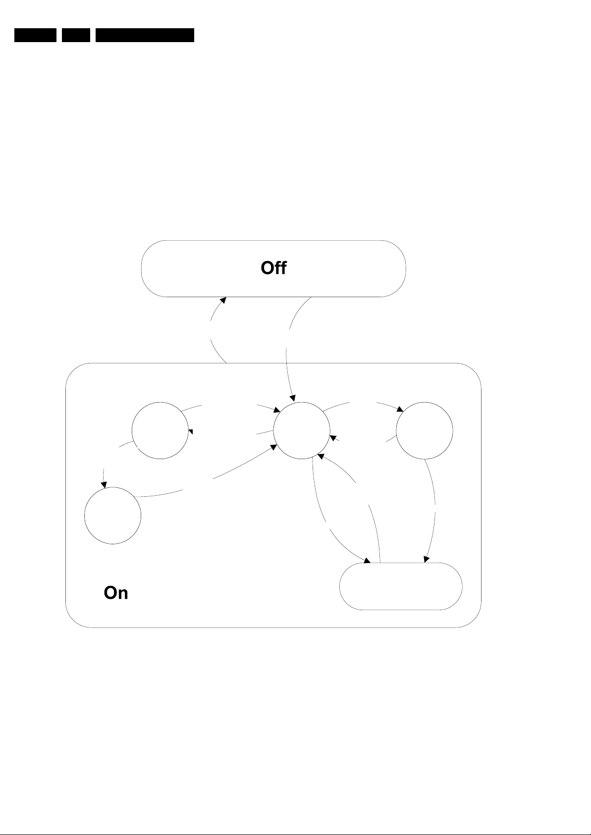
There are two possible situations: one for protections detected
by the stand-by software and one for protections detected by
the main software.
When the TV is in a protection state due to an error detected by
stand-by software (and thus blinking an error) and SDM is
activated via short-circuiting the pins on the SSB, the TV starts
up until it reaches the situation just before protection. So, this
is a kind of automatic stepwise start-up. In combination with the
start-up diagrams below, you can see which supplies are
present at a certain moment. Important to know is, that if e.g.
the 3V3 detection fails (and thus error 8 is blinking) and the TV
is restarted via SDM, the Stand-by Processor will enable the
3V3, but will not go to protection now. The TV will stay in this
situation until it is reset (Mains/AC Power supply interrupted).
Caution: in case the start up in this mode with a faulty FET
7U08 is done, you can destroy all IC’s supplied by the +3V3,
Mains
off
due to overvoltage. It is recommended to measure first the FET
7U08 on short-circuit before activating SDM via the service
pads.
When the TV is in protection state due to an error detected by
main software (MIPS protection) and SDM is activated via
short-cutting the service pads on the SSB, the TV starts up and
ignores the error.
In this chassis, only error “63” (power-ok) is a MIPS protection
and already displays the failure via blinking LED.
The abbreviations “SP” and “MP” in the figures stand for:
• SP: protection or error detected by the Stand-by
Processor.
• MP: protection or error detected by the MIPS Main
Processor.
Mains
on
- Tact switch Pushed
- last status is hibernate
after mains ON
Hibernate
St by
- WakeUp requested
- Acquisition needed
- No data Acquisition
required
- tact SW pushed
- last status is hibernate
after mains ON
Tact switch
pushed
Figure 5-3 Transition diagram
Semi
St by
GoTo Protection
WakeUp
requested
- St by requested
- tact SW pushed
WakeUp
requested
(SDM)
Protection
Active
GoTo Protection
I_17960_061.eps
220508
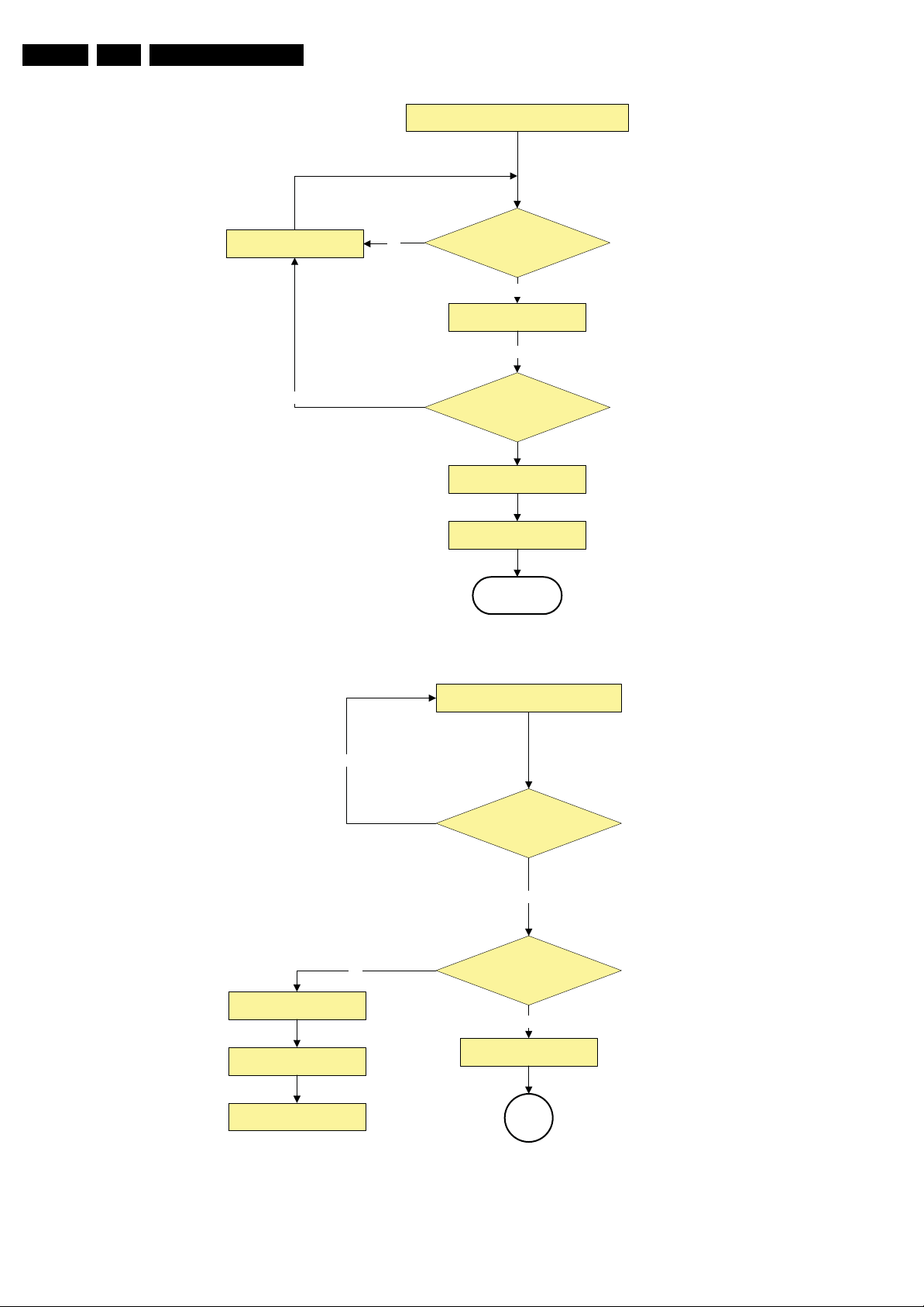
Page 21
Service Modes, Error Codes, and Fault Finding
EN 21Q528.2E LA 5.
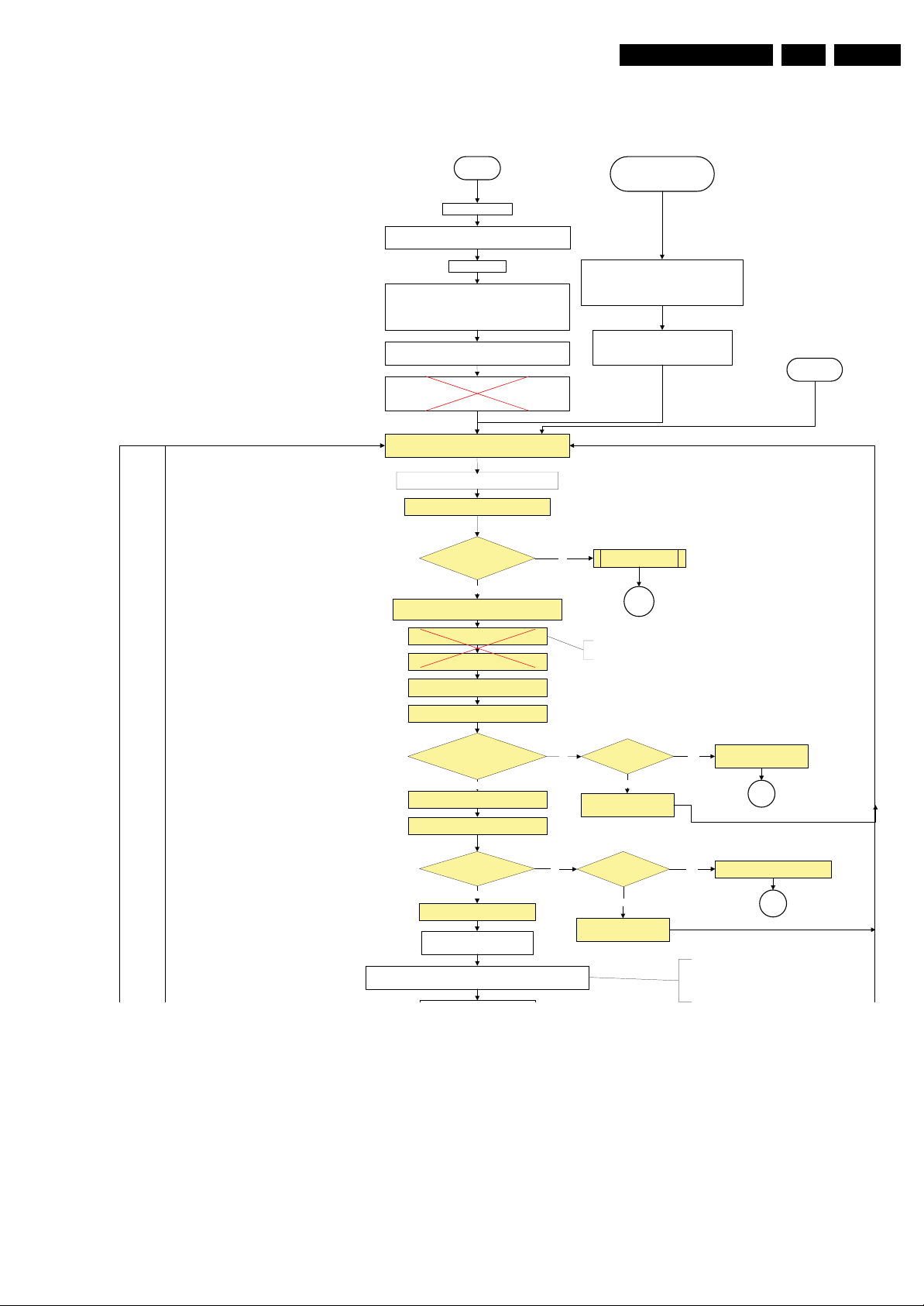
Off
Mains is applied
Standby Supply starts running.
All standby supply volt ages become available.
st-by µP resets
All I/O lines have a High default state:
- Switch PNX8541 in reset (active LOW).
- Keep the Audio-reset high.
- NVM power line is high, no NVM communication possible.
Initialise I/O pins of the st-by µP, start keyboard scanning, RC
detection. Wake up reasons are off.
PDPGO line is high (either HW wise in a non FHP set or
because of the stby µP reset in an FHP set) which will start the
Switch ON PSU supply by switching LOW the Standby I/O
Wait 50ms and then start polling the DETECT 2
FHP PDP.
line.
+12V is switched on
every 40ms.
2900 ms
Yes
activate DETECT 2 algo rithm
Enable the +1V2 supply (ENABLE-1V2)
Wait 100ms
Enable the supply for
+3V3 and +5V (ENABLE-3V3)
Start polling the detect 1
every 40ms
Stand by or
Protection
If the protection state was left by short circuiting the
SDM pins, detection of a protection condition during
startup will stall the startup. Protection conditions in a
playing set will be ignored. The protection mode will
No
not be entered.
- Switch Audio-Reset high.
It is low in the standby mode if the standby
mode lasted longer than 10s.
12V supply” error 6DETECT 2 received within
SP
Enable-1V2 is reserved , not use in
TV522-82M
Restart
DETECT 1 = High
within
250 ms after enable-3V3 toggle?
Yes
Activate DETECT 1 algorithms
Wait 20ms
SUPPLY-FAULT I/O line
is High?
Yes
Enable the supply fault detection
algorithm
No
Switch LOW the RESET-NVM_WP-NANDFLASH line. Add a 2ms delay
before trying to address the NVM to allow correct NVM initialization.
Set I²C slave address
of Standby µP to (A0h)
No
Standby line set to HIGH for 5
No
Detect 1 = High?
Standby line set to HIGH for 5
No
seconds
No
seconds
Voltage output error: 8Supply Fault = High? Yes
SP
Yes
Supply fault error 9
SP
This will allow access to NVM and
NAND FLASH and can not be done
earlier because the FLASH needs to
be in Write Protect as long as the
supplies are not available.
I_17960_062a.eps
230508
Figure 5-4 “Off” to “Semi Stand-by” flowchart (part 1)
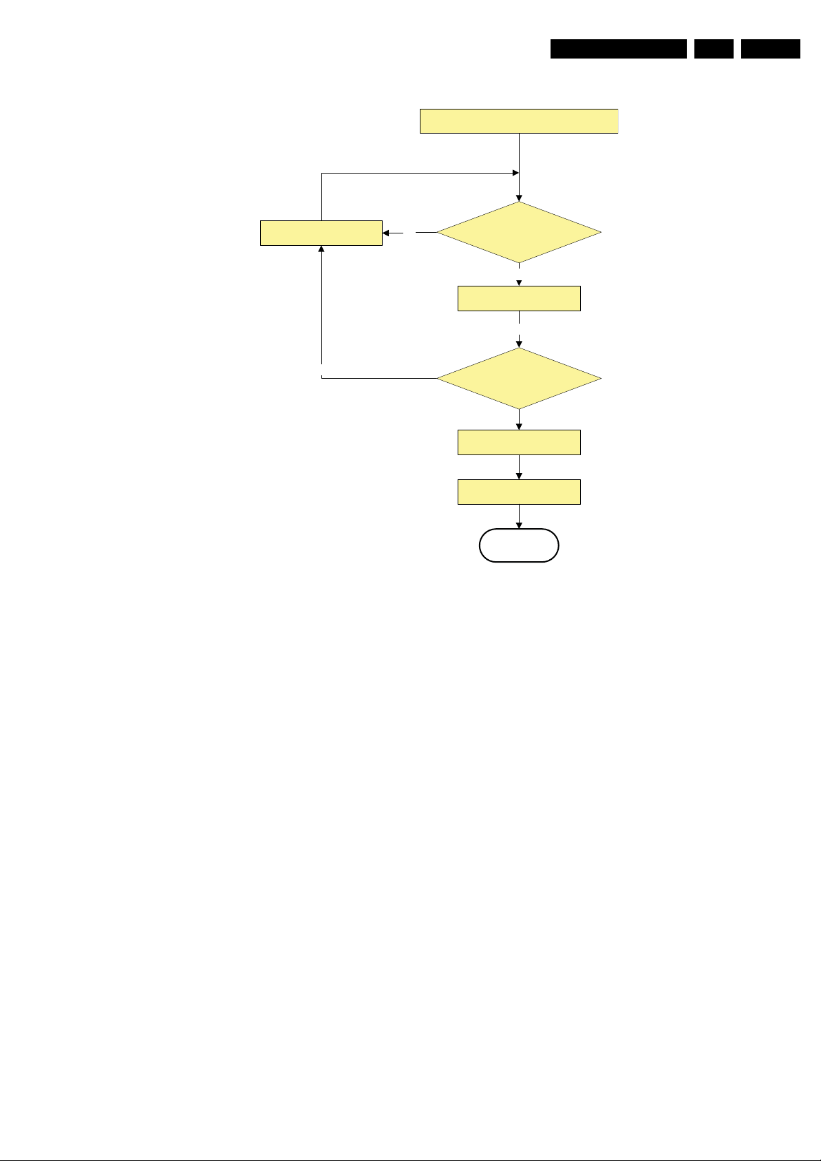
Page 22
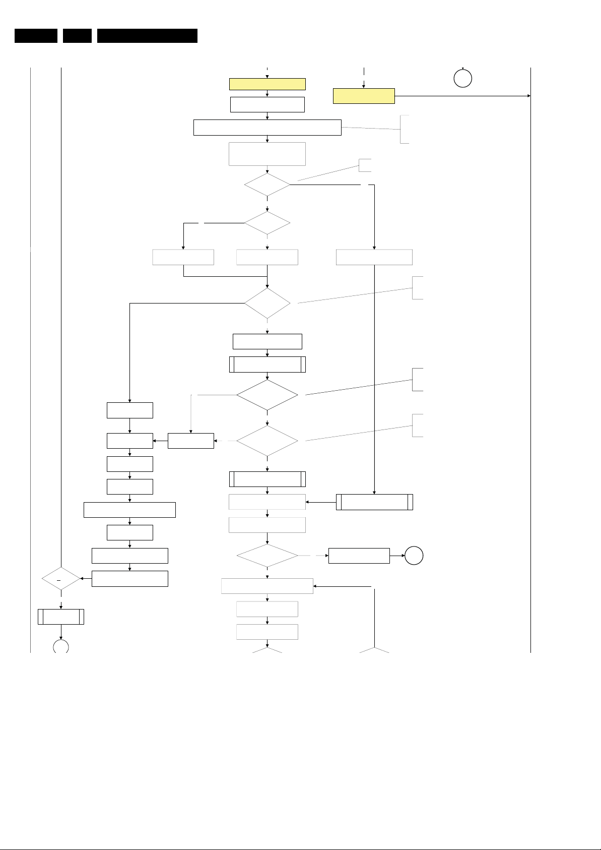
EN 22 Q528.2E LA5.
Service Modes, Error Codes, and Fault Finding
Yes
Enable the supply fault detection
algorithm
No
Switch LOW the RESET-NVM_WP-NANDFLASH line. Add a 2ms delay
before trying to address the NVM to allow correct NVM initialization.
No
No
Code = 5
Switch AVC PNX8541
in reset (active low)
Wait 10ms
Switch the NVM reset
line HIGH.
Disable all supply related protections and
switch off the +2V5, +3V3 DC/DC converter.
Wait 5ms
No
Release AVC system reset
Feed warm boot script
No
Code = 53
Set I²C slave address
of Standby µP to (A0h)
Detect EJTAG debug probe
(pulling pin of the probe interface to
ground by inserting EJTAG probe)
EJTAG probe
connected ?
No
Cold boot?
Yes
Release AVC system reset
Feed cold boot script
Bootscript ready
in 1250 ms?
Yes
Set I²C slave address
of Standby µP to (60h)
RPC start (comm. protocol)
RPC start (comm. protocol)
Flash to Ram image
transfer succeeded
within 30s?
Yes
SW initialization
No
succeeded
within 20s?
Yes
Enable Alive check mechanism
MIPS reads the wake up reason
from standby µP.
In case of an LCD set, check the
Power-OK display line
No
Standby line set to HIGH for 5
seconds
An EJTAG probe (e.g. WindPower ICE probe) can
be connected for Linux Kernel debugging purposes.
Yes
Release AVC system reset
Feed initializing boot script
disable alive mechani sm
Wait until AVC starts to
communicate
SP
This will allow access to NVM and
NAND FLASH and can not be done
earlier because the FLASH needs to
be in Write Protect as long as the
supplies are not available.
This is still the timing of the
Jaguar 2k6. Timing need to be
updated if more mature info is
available.
This is still the timing of the
This is still the timing of the
Jaguar 2k6. Timing needs to
Jaguar 2k6. Timing needs to
be updated if more mature info
be updated if more mature info
is available.
This is still the timing of the
Jaguar 2k6. Timing needs to
be updated if more mature info
is available.
3-th try?
Yes
Blink Code as
error code
SP
switch off the remaining DC/DC
converters
Switch Standby
I/O line high.
Power-ok display high?
Yes
Reset the Pacific by pulling LOW the Pacific
hardware reset line during 100ms.
Release Pacific reset
and wait 200ms
Ping the Pacific through I²C
Log power-ok error and enter
No
protection
No
Figure 5-5 “Off” to “Semi Stand-by” flowchart (part 2)
MP
I_17960_062b.eps
230508
Page 23
Service Modes, Error Codes, and Fault Finding
Y
EN 23Q528.2E LA 5.
es
Blink Code as
error code
Release Pacific reset
and wait 200ms
Ping the Pacific through I²C
SP
Pacific acknowledges?
Yes
Initialize Pacific
Enable the Pacific output by sending the PanelConfig.PanelOn
to the Pacific in case of a DFI set
Start 4 seconds preheating timer in case of
an LPL scanning backlight LCD set.
Initialize audio
- Channeldecoder type TDA10060
cannot be reloaded without reset
of the channeldecoder.
- Channeldecoder type TDA10048
can be reloaded without reset.
No
Channel decoder
TDA 10048?
No
Third try?
Yes
Log channel decoder error
Yes
No
Download firmware into the channel
decoder
Downloaded
successfully?
Yes
initialize tuner, Master IF and channel
decoder
No
Third Pacific boot retry?
Yes
Log Pacific error
This is needed here because the
Pacific has to deliver an output
clock towards the DFI. Otherwise
the DFI cannot deliver ambilight
functionality in the lampadaire
mode. The presence of the DFI
can be determined via the display
option.
Release reset MPEG4 module:
BOLT-ON-IO: High
MPEG4 module will start booting
autonomously.
Wait TBD ms
POR polling positive?
No
Log SW event:
STi7100PorFailure
Important remark:
Input vertical frequency
changes (48/50/60Hz)
detected during startup
sequence should not be
taken into account. The
end situation should
always be safeguarded. If
not, these changes will
lead to EPLD resets which
will switch on the display
and disturb the startup
performance.
Figure 5-6 “Off” to “Semi Stand-by” flowchart (part 3)
Initialize source selection
Wait until Cpipe del ivers a stable output
initialize AutoTV by triggering CHS AutoTV Init interface
Initialize Pacific or EPLD related Ambilight
Do not enter semi-standby state in case of an LPL
scanning backlight LCD set before 4s preheating timer has
elapsed.
clock
Reset EPLD
Wait 100ms
Reset Pacific clock
Initialize video processing IC's:
- PNX5050 in /82
-scaler EPLD
settings (if applicable)
Initialize Ambilight with Lights off.
Semi-Standby
yes
EPLD
and
Pacific
should
be reset
when a
stable
input
clock
become
s
available
at their
input.
Start alive IIC po lling
mechanism
Alive
polling
NOK
Log SW event
STi7100AliveFailedError
and generate fast cold
reboot eventually
followed by a cold reboot.
Because of a bug in the Pacific IC, all video and
display related Pacific parameters should be
initialized before initializing the ambilight related
Pacific parameters. If not, initializing the video and
display related Pacific parameters will overwrite the
ambilight parameters.
yes
Wait TBD ms
POR polling positive?
No
bootSTi7100PorFailure:
Log HW error 38 and
generate cold boot
I_17960_062c.eps
230508
Page 24
EN 24 Q528.2E LA5.
Service Modes, Error Codes, and Fault Finding
Semi Standby
Wait until previous on-state is left more than 2
seconds ago. (to prevent LCD display problems)
Assert RGB video blanking
and audio mute
Rewrite Pacific register 0x03 (output format) with TcuUpdate:
this command is sometimes not processed properly by the
Pacific at initialisation time, resending it here solves the issue.
Switch on the display by sending the
PanelConfig.PanelOn (I²C) command to the Pacific
wait 250ms (min. = 200ms)
Switch off the dimming backlight feature and
make sure PWM output is set to 100%
action holder: AVC
action holder: St-by
autonomous action
Initialize audio and video
processing IC's and functions
according needed use case.
Switch on LCD backlight
The higher level requirement is that
audio and video should be demuted
without transient effects and that the
audio should be demuted maximum 1s
before or at the same time as the
unblanking of the video.
Wait until valid and stable audio and video, corresponding to
the requested output is delivered by the AVC AND the
backlight PWM has been on for 1second.
Switch Audio-Reset low and wait 5ms
Release audio mute and wait 100ms before any other audio
handling is done (e.g. volume change)
Restore dimming backlight feature, PWM output and unblank
the video.
Active
I_17960_063.eps
220508
Figure 5-7 “Semi Stand-by” to “Active” flowchart (non DFI)
Page 25
Service Modes, Error Codes, and Fault Finding
EN 25Q528.2E LA 5.
Active
Mute all sound outputs via softmute
Wait 100ms
Set main amplifier mute (I/O: audio-mute)
Force ext audio outputs to ground
(I/O: audio reset)
And wait 5ms
switch off LCD backlight
Mute all video outputs
action holder: AVC
action holder: St-by
autonomous action
Wait 250ms (min. = 200ms)
Switch off the display by sending the
PanelConfig.PanelOff (I²C) command to the Pacific
switch off ambient light
Semi Standby
Figure 5-8 “Active” to “Semi Stand-by” flowchart (non-DFI)
I_17960_064.eps
220508
Page 26
EN 26 Q528.2E LA5.
Service Modes, Error Codes, and Fault Finding
Semi Stand by
If ambientlight functionality was used in semi-standby
(lampadaire mode), switch off ambient light (see CHS
ambilight)
Delay transition until ramping down of ambient light is
finished. *)
transfer Wake up reasons to the Stand by µP.
Switch Memories to self-refresh (this creates a more
stable condition when switching off the power).
Switch AVC system in reset state
Wait 10ms
Switch the NVM reset line HIGH.
Disable all supply related protections and switch off
the DC/DC converter (via the Enable-3V3 I/O line)
Wait 5ms
*) If this is not performed and the set is
switched to standby when the switch off of
the ambilights is still ongoing, the lights will
switch off abruptly when the supply is cut.
Important remark:
release reset audio 10 sec after
entering standby to save power
switch off the +1V2 DC/DC converters
Switch OFF all supplies by switching HIGH the
standby I/O line..
Stand by
Figure 5-9 “Semi Stand-by” to “Stand-by” flowchart
I_17960_065.eps
220508
Page 27
Service Modes, Error Codes, and Fault Finding
EN 27Q528.2E LA 5.
action holder: MIPS
action holder: St-by
autonomous action
MP
Log the appropriate error and
set stand-by flag in NVM
Redefine wake up reasons for protection
state and transfer to stand-by µP.
Switch off LCD lamp supply
Wait 250ms (min. = 200ms)
Switch off LVDS signal
Switch off 12V LCD supply within a time frame of
min. 0.5ms to max. 50ms after LVDS switch off.
Ask stand-by µP to enter protection state
SP
Switch AVC in reset state
Wait 10ms
Switch the NVM reset line HIGH.
Disable all supply related protections and switch off
the +1V8 and the +3V3 DC/DC converter.
Wait 5ms
switch off the +1V2 DC/DC converter
Switch OFF all supplies by switching HIGH the
Standby I/O lines.
Flash the Protection-LED in order to indicate
protection state*
(*): This can be the standby LED or the ON LED
depending on the availability in the set under
discussion.
Protection
Figure 5-10 “Protection” flowchart
I_17960_066.eps
220508
Page 28
EN 28 Q528.2E LA5.
Service Modes, Error Codes, and Fault Finding
supply detection algorithms for DC-DC outputs
Polling every 40ms
No
No
DETECT 1 = Low ?
Yes
Check DETECT1 5 times
( within 500us )
Yes
DETECT 1 = Low ?
5 consecutive times ?
Shutdown ( Active to
Semistdby to standby )
Wait for 5 seconds
Restart
I_17960_067.eps
220508
Figure 5-11 “Supply detection algorithm for DC-DC outputs” flowchart
Shutdown ( Active to
Semistdby to standby )
Wait for 5 seconds
Restart
N0
No
supply fault detection algorithm
SUPPLY-FAULT = LOW for
1ms ?
Yes
DETECT1 = High ?
Yes
Error 9
SP
I_17960_068.eps
220508
Figure 5-12 “Supply fault detection algorithm” flowchart
Page 29
Service Modes, Error Codes, and Fault Finding
EN 29Q528.2E LA 5.
Polling every 40ms
No
detection algorithm. See CHS protections.
No
+12V supply
DETECT 2 = Low ?
Yes
Check DETECT2 5 times
( within 500us)
Yes
DETECT 2 = Low ?
5 consecutive times ?
Shutdown ( Active to
Semistdby to standby )
Wait for 5 seconds
Restart
I_17960_069.eps
Figure 5-13 “+12 V supply detection algorithm” flowchart
220508
Page 30
EN 30 Q528.2E LA5.
Service Modes, Error Codes, and Fault Finding
5.4 Service Tools
5.4.1 ComPair
Introduction
ComPair (Computer Aided Repair) is a Service tool for Philips
Consumer Electronics products. and offers the following:
1. ComPair helps you to quickly get an understanding on how
to repair the chassis in a short and effective way.
2. ComPair allows very detailed diagnostics and is therefore
capable of accurately indicating problem areas. You do not
have to know anything about I
yourself, because ComPair takes care of this.
3. ComPair speeds up the repair time since it can
automatically communicate with the chassis (when the uP
is working) and all repair information is directly available.
4. ComPair features TV software up possibilities.
Specifications
ComPair consists of a Windows based fault finding program
and an interface box between PC and the (defective) product.
The (new) ComPair II interface box is connected to the PC via
an USB cable. For the TV chassis, the ComPair interface box
and the TV communicate via a bi-directional cable via the
service connector(s).
How to Connect
This is described in the ComPair chassis fault finding database.
TO
ComPair II
RC in
Optional
Switch
Power ModeLink/
Activity
UART SERVICE
RC out
CONNECTOR
I2C SERVICE
CONNECTOR
Multi
function
TO TV
TO
2
C or UART commands
TO
UART SERVICE
CONNECTOR
2
I
C
RS232 /UART
5.5 Error Codes
5.5.1 Introduction
The error code buffer contains all detected errors since the last
time the buffer was erased. The buffer is written from left to
right, new errors are logged at the left side, and all other errors
shift one position to the right.
When an error occurs, it is added to the list of errors, provided
the list is not full. When an error occurs and the error buffer is
full, then the new error is not added, and the error buffer stays
intact (history is maintained).
To prevent that an occasional error stays in the list forever, the
error is removed from the list after more than 50 hrs. of
operation.
When multiple errors occur (errors occurred within a short time
span), there is a high probability that there is some relation
between them.
Basically there are three kinds of errors:
• Errors detected by the Stand-by software. These errors
will always lead to protection and an automatic start of the
blinking LED for the concerned error (see paragraph “The
Blinking LED Procedure”). In these cases SDM can be
used to start up (see chapter “Stepwise Start-up”). Note
that it can take up to 90 seconds before the TV goes to
protection and starts blinking the error (e.g. error 53)
• Errors detected by main software that lead to
protection. In this case the TV will go to protection and the
front LED should also blink the concerned error. See also
paragraph “Error Codes” -> “Error Buffer” -> “Extra Info”.
For this chassis only error 63 is a protection error detected
by main software.
• Errors detected by main software that do not lead to
protection. In this case the error will be logged into the
error buffer and can be read out via ComPair, via blinking
LED method, or in case you have picture, via SAM.
5.5.2 How to Read the Error Buffer
PC
ComPair II Developed by Philips Brugge
Optional power
HDMI
2
I
C only
5V DC
E_06532_036.eps
Figure 5-14 ComPair II interface connection
Caution: It is compulsory to connect the TV to the PC as
shown in the picture above (with the ComPair interface in
between), as the ComPair interface acts as a level shifter. If
one connects the TV directly to the PC (via UART), ICs will be
blown!
How to Order
ComPair II order codes:
• ComPair II interface: 3122 785 91020.
• ComPair32 CD (update): 3122 785 60160.
• ComPair RS232 cable: 3104 311 12742 (to be used with
chassis Q52x).
Note: If you encounter any problems, contact your local
support desk.
5.4.2 LVDS Tool
Support of the LVDS Tool has been discontinued.
150208
Use one of the following methods:
• On screen via the SAM (only if you have a picture). E.g.:
– 00 00 00 00 00: No errors detected
– 06 00 00 00 00: Error code 6 is the last and only
detected error
– 09 06 00 00 00: Error code 6 was first detected and
error code 9 is the last detected error
• Via the blinking LED procedure (when you have no
picture). See next paragraph.
•Via ComPair.
• Via CSM. when CSM is activated the blinking LED
procedure will start and the CSM content will be written to
a USB stick (if present).
5.5.3 How to Clear the Error Buffer
Use one of the following methods:
• By activation of the “RESET ERROR BUFFER” command
in the SAM menu.
• With a normal RC, key in sequence “MUTE” followed by
“062599” and “OK”.
• If the content of the error buffer has not changed for 50+
hours, it resets automatically.
5.5.4 Error Buffer
In case of non-intermittent faults, clear the error buffer before
you begin the repair (before clearing the buffer, write down the
content, as this history can give you significant information).
This to ensure that old error codes are no longer present.
If possible, check the entire contents of the error buffer. In
some situations, an error code is only the result of another error
Page 31

Service Modes, Error Codes, and Fault Finding
EN 31Q528.2E LA 5.
code and not the actual cause (e.g., a fault in the protection
detection circuitry can also lead to a protection).
There are several mechanisms of error detection:
• Via error bits in the status registers of ICs.
• Via polling on I/O pins going to the stand-by processor.
• Via sensing of analogue values on the stand-by processor
or the PNX85xx.
• Via a “not acknowledge” of an I
2
C communication.
Take notice that some errors need more than 90 seconds
before they start blinking or before they will be logged. So in
case of problems wait 2 minutes from start-up onwards, and
then check if the front LED is blinking or if an error is logged.
Table 5-2 Error code overview
Error Description Error/
3I2C3 E MIPS PNX85xx Error logged.
5 PNX85xx does
not boot (HW
cause)
6 5V, 12V supply P Stby P / Protection + Error
8 1V2, 1V4, 2V5,
3V3 supply
9 Supply fault P Stby P / Protection + Error
2
C-MUX1 E MIPS PCA9540 Error logged.
11 I
2
12 I
C-MUX2 E MIPS PCA9540 Error logged.
22 PNX5050 E MIPS PNX5050 Error logged.
23 HDMI mux E MIPS AD8190/
2
C switch E MIPS PCA9540 Error logged.
24 I
26 Master IF E MIPS TDA9898/
28 MOP (Ambilight
MOP on DFI
1)
panel)
34 Tuner E MIPS TD1716 Error logged.
37 Channel decoder E MIPS TDA10060/
46 Pacific3 E MIPS T6TF4 Error blinking + Error
53 PNX85xx does
not boot (SW
cause)
63 Power OK E/P MIP S / Error logged in case of
65 DFI (EPLD on
DFI panel)
1)
Detected
by
Device Result
blinking.
blinking.
blinking.
AD8191
9897/9890
84C7N
TDA10048
Error logged.
Error logged.
Error logged.
Error logged.
logged.
a PDP set. Protection
in case of an LCD set.
logged.
Prot
E Stby P PNX85xx Error blinking.
P Stby P / Protection + Error
E MIPS EP2CXXF4
E Stby P PNX85xx Error blinking.
E MIPS / Error blinking + Error
Note
1). Where applicable.
Extra Info
• Rebooting. When a TV is constantly rebooting due to
internal problems, most of the time no errors will be logged
or blinked. This rebooting can be recognized via a ComPair
interface and Hyperterminal (for Hyperterminal settings,
see paragraph “Stand-by software upgrade). You will see
that the loggings which are generated by the main software
keep continuing. In this case (rebooting) diagnose has to
be done via ComPair.
• Error 3 (I
2
C bus 3 blocked). At the time of release of this
manual, this error was not working as expected (error 3 is
logged and can be read out). Current situation: when this
error occurs, the TV will constantly reboot due to the
blocked bus. The best way for further diagnosis here, is to
use ComPair (e.g. read out the NVM content). Instead of
error “3” it is possible you will see error “2” in the error
buffer.
• Error 5 (PNX85xx doesn’t boot). Indicates that the main
processor was not able to read his bootscript. This error will
point to a hardware problem around the PNX85xx (supplies
not OK, PNX 8535 completely dead, I
2
C link between PNX
and Stand-by Processor broken, etc...). When error 5
occurs it is also possible that I
2
I
C2 can be indicated in the schematics as follows: SCL-
2
C2 bus is blocked (NVM).
UP-MIPS, SDA-UP-MIPS, SCL-SLAVE, SDA-SLAVE,
SCL-2 or SDA-2.
• Error 11 (I
2
I
C-MUX1 bus. At the time of release of this manual, this
2
C MUX1). Indicates a blocked (short circuited)
error was not working as expected. Current situation: when
this error occurs the TV will constantly reboot due to the
blocked bus. The best way for further diagnosis, is to use
ComPair (e.g. read out the NVM content).
• Error 12 (I
2
I
C-MUX2 bus. At the time of release of this manual, this
2
C MUX2). Indicates a blocked (short circuited)
error was not working as expected. Current situation: when
this error occurs the TV will constantly reboot due to the
blocked bus. The best way for further diagnosis, is to use
ComPair (e.g. read out the NVM content).
• Error 24 (I
2
C switch). As a side effect of error 24 it is
possible that error 47(no existing error) will also be logged.
• Error 28 (DFI Ambilight MOP). It can take up to 2 minutes
or more before this error is logged. So if you suspect that
this MOP is defective: clear the error buffer, restart the TV
and wait for about 2 minutes before checking the error
buffer.
• Error 37 (Channel decoder). When this error occurs,
there probably will be no picture and sound from tuner
input. As a side effect of error 37 it is possible that error 4
(no existing error) is also logged.
• Error 46 (Pacific 3). When there is an actual problem with
or around the Pacific during start-up, you will have no
picture and error 46 will be blinked via the blinking LED
procedure. For further diagnosis you can always dump the
CSM content on USB stick (see CSM) or use ComPair.
• Error 53. This error will indicate that the PNX85xx has read
his bootscript (if this would have failed, error 5 would blink)
but initialization was never completed because of hardware
problems (NAND flash, ...) or software initialization
problems. Possible cause could be that there is no valid
software loaded (try to upgrade to the latest main software
version). Note that it can take up to 2 minutes before the TV
starts blinking error 53.
• Error 63 (POWER OK). When this error occurs, it means
that the POWER-OK line did not became “high”. This error
is only applicable for TV’s with an LCD display. For PDP
displays there will be no protection during a POWER-OK
line failure, but error 63 will be logged in the error buffer.
Caution: in case a PDP TV ends up into power-ok
protection, it can indicate that the display option code is set
to “LCD”. To change the display option code to “PDP” you
need to activate SDM via the service pads (see figure
“Service mode pads”). Then change the display option
code blindly via a standard RC: key in the code “062598”
directly followed by the “MENU” button and “XXX” (where
XXX is the 3 digit decimal display option code as
mentioned in figure “Display option code overview”).
• Error 65 (DFI EPLD error). When this error occurs it
means that there is a problem with the I
2
C communication
towards the EPLD (picture processing EPLD, not the
Ambilight EPLD) on the DFI panel.
Page 32

EN 32 Q528.2E LA5.
Service Modes, Error Codes, and Fault Finding
5.6 The Blinking LED Procedure
5.6.1 Introduction
The blinking LED procedure can be split up into two situations:
• Blinking LED procedure in case of a protection. In this case
the error is automatically blinked. This will be only one
error, namely the one that is causing the protection.
Therefore, you do not have to do anything special, just read
out the blinks. A long blink indicates the decimal digit, a
short blink indicates the units.
• Blinking LED procedure in the “on” state. Via this
procedure, you can make the contents of the error buffer
visible via the front LED. This is especially useful for fault
finding, when there is no picture.
When the blinking LED procedure is activated in the “on” state,
the front LED will show (blink) the contents of the error-buffer.
Error-codes > 10 are shown as follows:
1. “n” long blinks (where “n” = 1 - 9) indicating decimal digit,
2. A pause of 1.5 s,
3. “n” short blinks (where “n”= 1 - 9),
4. A pause of approx. 3 s,
5. When all the error-codes are displayed, the sequence
finishes with a LED blink of 3 s,
6. The sequence starts again.
Example: Error 12 8 6 0 0.
After activation of the SDM, the front LED will show:
1. 1 long blink of 750 ms (which is an indication of the decimal
digit) followed by a pause of 1.5 s,
2. 2 short blinks of 250 ms followed by a pause of 3 s,
3. 8 short blinks followed by a pause of 3 s,
4. 6 short blinks followed by a pause of 3 s,
5. 1 long blink of 3 s to finish the sequence,
6. The sequence starts again.
5.6.2 How to Activate
Use one of the following methods:
• Activate the SDM or CSM. The blinking front LED will
show the entire contents of the error buffer (this works in
“normal operation” mode).
• Transmit the commands “MUTE” - “062500” - “OK”
with a normal RC. The complete error buffer is shown.
Take notice that it takes some seconds before the blinking
LED starts.
• Transmit the commands “MUTE” - “06250x” - “OK”
with a normal RC (where “x” is a number between 1 and
5). When x= 1 the last detected error is shown, x= 2 the
second last error, etc.... Take notice that it takes some
seconds before the blinking LED starts.
5.7 Protections
5.7.1 Software Protections
Most of the protections and errors use either the stand-by
microprocessor or the MIPS controller as detection device.
Since in these cases, checking of observers, polling of ADCs,
and filtering of input values are all heavily software based,
these protections are referred to as software protections.
There are several types of software related protections, solving
a variety of fault conditions:
• Protections related to supplies: check of the 12V, +5V,
+1V2, +1V4, 2V5 and +3V3.
• Protections related to breakdown of the safety check
mechanism. E.g. since the protection detections are done
by means of software, failing of the software will have to
initiate a protection mode since safety cannot be
guaranteed any more.
Remark on the Supply Errors
The detection of a supply dip or supply loss during the normal
playing of the set does not lead to a protection, but to a cold
reboot of the set. If the supply is still missing after the reboot,
the TV will go to protection.
Protections during Start-up
During TV start-up, some voltages and IC observers are
actively monitored to be able to optimise the start-up speed,
and to assure good operation of all components. If these
monitors do not respond in a defined way, this indicates a
malfunction of the system and leads to a protection. As the
observers are only used during start-up, they are described in
the start-up flow in detail (see paragraph “Stepwise Start-up”).
5.7.2 Hardware Protections
The only real hardware protection in this chassis is (in case of
an audio problem) the audio protection circuit that will switch
“off” immediately the supply of the SSB. The supply will buzz
during the protection and +12VS drops to approx. 5V5 and +5V
Stand-by to approx. to 1V9. Other indication of the audio
protection is that the red LED lights up with an intensity of 50%.
Repair Tips
• It is also possible that you have an audio DC protection
because of an interruption in one or both speakers (the DC
voltage that is still on the circuit cannot disappear through
the speakers). Caution: (dis)connecting the speaker wires
during the ON state of the TV at high volume can damage
the audio amplifier.
5.8 Fault Finding and Repair Tips
Read also paragraph “Error Codes” -> “Error Buffer” -> “Extra
Info”.
5.8.1 Ambilight
Due to a degeneration process of the AmbiLight, it is
recommended to change all ambilight units in case one unit
needs to be repaired.
5.8.2 CSM
When you activate CSM and there is a USB stick connected to
the TV, the software will dump the complete CSM content to the
USB stick. The file (Csm.txt) will be saved in the root of your
USB stick. If this mechanism works you can conclude that a
large part of the operating system is already working (MIPS,
USB...)
Page 33

Service Modes, Error Codes, and Fault Finding
EN 33Q528.2E LA 5.
5.8.3 DC/DC Converter
Introduction
• The best way to find a failure in the DC-DC converters is to
check their starting-up sequence at “power-on via the
mains cord”, presuming that the standby microprocessor is
operational.
• If the input voltage of DC-DC converters is around 12.7V
(measured on decoupling capacitors 2U0W and 2U0Y and
the enable signals are "low" (active) then the output
voltages should have their normal values. +12Vand +5VPOD supplies start-up first (enabled by PODMODE signal
from the standby microprocessor). There is a
supplementary condition for +12V to start-up: if +5V-POD
does not start up due to a local defect, then +12V will not
be available as well. +5V-ON supply is enabled by the
ONMODE signal (coming also from the standby
microprocessor) . +1V2 supply starts-up when +12V
appears, then at least 100 ms later, +1V8, +2V5 and+3V3
will be activated via the ENABLE-3V3 signal from the
standby microprocessor. If +12V value is less than 10 V
then the last enumerated voltages will not show-up due to
the under-voltage detection circuit 7U01-1 + 6U04 and
surrounding components. Furthermore, if +12V is less than
8V then also +1V2 will not be available. The third DC-DC
convertor that delivers +1V4 out of +12V is started up when
the ENABLE-1V2 becomes active (low) and +12V is
present. The +Vtun generator (present only for the
analogue version of China platforms) will generate +33V
for the analogue tuner as soon as the 12V/3.3V DC-DC
converter will start to operate.
• The consumption of controller IC 7U0A is around 19 mA
(that means almost 200 mV drop voltage across resistor
3U70) and the consumption of controller IC 7U0L is around
12 mA.
• The current capability of DC-DC converters is quite high
(short-circuit current is 7 to 10 A), therefore if there is a
linear integrated stabiliser that, for example, delivers 1.8V
from +3V3 with its output overloaded, the +3V3 stays
usually at its normal value even though the consumption
from +3V3 increases significantly.
• The +1V8 and +2V5 supply voltages are obtained via linear
stabilizer made with discrete components that can deliver
a lot of current, therefore in case +1V8 or +2V5 are
shortcircuited to GND then +3V3 will not have the normal
value but much less.
• The SUPPLY-FAULT signal (active low) is an internal
protection (error 9) of the DC-DC convertor and will occur
if the output voltage of any DC-DC convertor is out of limits
(10% of the normal value).
Fault Finding
• Symptom: +1V2 not present (even for a short while ~10
ms)
1. Check 12 V availability (resistor 3U70, MOS-FETs 7U05
and 7U06), value of +12 V, and surrounding components)
2. Check the voltage on pin 9 (1.5 V),
3. Check for +1V2 output voltage short-circuit to GND that
can generate pulsed over-currents 7...10 A through coil
5U00.
4. Check the over-current detection circuit (2U00 or 3U17
interrupted).
• Symptom: +1V4 not present (even for a short while
~10ms) while +12V is okay (also across input capacitors
2U8A and 2U8E).
1. Check resistor 3U3T and power MOS-FETs 7U0D-1/2 .
2. Check the voltage on pin 4 (4 V).
3. Check enable signal ENABLE-1V2 (active "low").
4. Check for +1V4 output voltage short-circuit to GND that
can generate pulsed over-currents 7...10 A through coil
5U05.
• Symptom: +1V2 present for about 100ms, +1V8, +2V5
and +3V3 not rising.
1. Check the ENABLE-3V3 signal (active "low"),
2. Check the voltage on pin 8 (1.5 V),
3. Check the under-voltage detection circuit (the voltage on
collector of transistor 7U01-1 should be less than
0.8 V),
4. Check for output voltages short-circuits to GND (+3V3,
+2V5 and +1V8) that can generate pulsed overcurrents
7...10 A through coil 5U01,
5. Check the over-current detection circuit (2U04 or 3U14
interrupted).
• Symptom: +1V2 OK, +2V5 and +3V3 present for about
100 ms. Possible cause: SUPPLY-FAULT line stays “low”
even though the +3V3 and +1V2 is available - the standby
microprocessor is detecting that and switching "off" all
supply voltages.
1. Check the drop voltage across resistor 3U70 or 3U3T
(they could be too high, meaning a defective controller IC
or MOS-FETs),
2. Check if the boost voltage on pin 4 of controller IC 7U0A
is less than 14 V (should be 19 V),
3. Check if +1V2 or +3V3 are higher than their normal
values - that can be due to defective DC feedback of the
respective DC-DC convertor (ex. 3U1J, 3U75).
• Symptom: +1V2, +1V4, +1V8, +2V5 or +3V3 shows a high
level of ripple voltage (audible noise can come from the
filtering coils 5U00, 5U01 or 5U04). Possible cause:
instability of the frequency and/or duty cycle of a DC-DC
converter or stabilizer.
1. Check the resistor 3U0H and 3U2E, capacitors 2U0C
and 2U0A, input and output decoupling capacitors.
2. Check a.c. feedback circuits (2U08+2U09+3U07+3U08
for +1V2, 2U8P+2U0Y+3U24 for +1V4 and
2U03+2U05+3U04).
• Symptom: +1V2, +1V4, +2V5 and +3V3 ok, no +Vtun
(analogue sets only). Possible cause: the “+VTUN
GENERATOR” circuit (7U0P +7 U0Q + surroundings
components) is defective: check transistor 7U0P (it has to
have gate voltage pulses of about 10 V amplitude and drain
voltage pulses of about 35 V amplitude) and surrounding
components. A high consumption (more than 6 mA) from
+Vtun voltage can cause also +Vtun voltage to be too low
or zero.
Note: when a pair of power MOSFETs (7U02+7U08,
7U05+7U06 or 7U0D-1/2) becomes defective the controller IC
7U0A or 7U0L should be replaced as well.
5.8.4 Exit “Factory Mode”
When an “F” is displayed in the screen’s right corner, this
means that the set is in “Factory” mode, and it normally
happens after a new SSB has been mounted.
To exit this mode, push the “VOLUME minus” button on the
TV’s keyboard control for 5 seconds and restart the set.
Page 34

EN 34 Q528.2E LA5.
5.8.5 SSB Replacement
Follow the instructions in the flowchart in case you have to
exchange the SSB. See figure “SSB replacement flowchart”.
Service Modes, Error Codes, and Fault Finding
START
Set is still
operating?
Set is starting up but no display
Upgrade main TV SW to the latest version via
USB stick (#)
Program “Display Option” code via 062598
MENU, followed by 3 digits code (this code
can be found on a sticker inside the set or in
the Service Manual)
After entering “Display Option” code, set is
going to Standby (= validation of code)
Restart the set
Yes
No
Activate SAM and save the TV settings
via “Upload to USB”
- Replace SSB board by a Service SSB.
- Make the SSB fit mechanically to the set.
Start-up set
If necessary, adapt the connector plate and/or
the shielding to make the assy fit
mechanically.
Set behaviour?
Set is starting up & display is OK
Set goes into protection
Activate SDM via shorting the Service pins on
the SSB
- Program Display Option code via 062598 MENU followed by the 3 digit code
(see sticker inside set or in the Service Manual)
- Or program “Display Option” code in SAM via “062596 i+”, Options, Display, Screen
Method 1; In some sets it is possible to
program “Display Option” code before set is
going into protection.
If set is starting-up in Factory mode “F”, push
the “Volume minus” button on the local
keyboard for 5 seconds and restart the set
Method 2; First bring set in SDM and
program “Display Option” code.
Method 3; Bring the PDP power supply in
stand-alone mode and program the “Display
Option” code.
No
Connect ComPair, load JETT software and
program set type- and serial number
Update main and Standby software via USB
(#) Some new “Display Option” codes are not recognised
by SSB’s with old(er) SW, resulting in “no display”.
Therefore it is advised to ALWAYS update the main TV
SW (autorun.upg) via a USB stick to the latest version,
before setting the “Display Option” code
.
Figure 5-15 SSB replacement flowchart
Saved settings
on USB stick?
Yes
Activate SAM and reload settings
via “Download from USB”
Check latest software on Service website.
Check and perform alignments in SAM
according to the Service Manual
Check changes in CSM
END
In case of settings reloaded from USB, the set type- and
set serial number are automatically stored when entering
display options.
- Check if correct “Display Option” code is programmed.
- Verify “Option Codes” according sticker inside the set.
- Default settings for White drive ...see Service Manual
Instruction note SSB replacement
3122 785 00982
05-FEB-2007
H_16771_007.eps
130707
Page 35

Service Modes, Error Codes, and Fault Finding
5.8.6 Display option code
Caution: In case you have replaced the SSB, always check the
display option code in SAM, even if you have picture. With a
wrong display option code it is possible that you have picture,
but that in certain conditions you have unwanted side-effects.
5.8.7 Upgrade EDID NVM
To upgrade the EDID NVM you must short circuit pin 7 of the
EDID NVM to ground. Therefore some test points (EDID1,
EDID2 and EDID3) are foreseen next to the HDMI connectors
(figure “EDID-NVM pins”). See ComPair for further instructions.
EDID 3 EDID 2 EDID 1
Figure 5-16 EDID-NVM pins
EN 35Q528.2E LA 5.
H_17650_089.eps
160108
Nand Flash content
JFFS2 partition 1
(application read write data)
rtition 0
JFFS2 pa
(Application read only once data)
JFFS2 partition 0
(Application read only upgradable data)
SQUASHFS partition
BFFS partition 2 (DVD OK)
BFFS partition 1 (DVD cursor down)
BFFS partition 0
Block 0
hC
wizard pictures, display file, cabinet file,
upgrade assistant, …
Main
software (Mips)
Linux structure (root file system)
Default software upgrade application
TriMedia software
boot batch file 2
Back up software upgrade application
boot batch file 1
Linux kernel
JETT : needed for ComPair
Jaguar Boot loader
boot batch file 0
µBTM
partition table
Figure 5-17 NAND-Flash content
• The above overview of the NAND Flash shows the content
of the different partitions. It also shows which part of the
one-zip file erases and programs which part of the NAND
Flash.
• Remark: the above does not mean that you can reprogram
your HDMI keys with the “UpgradeAll.upg” file from the one
zip file. This can only be done in a secure environment (e.g.
the factory).
• The “UpgradeAll.upg” file is only used in the factory.
• The “FlashUtils.upg” file is only used by service centra
which are allowed to do component level repair on the
SSB.
Automatic Software Upgrade
In “normal” conditions, so when there is no major problem with
the TV, the main software and the default software upgrade
application can be upgraded with the “AUTORUN.UPG” (FUS
part of the one-zip file: e.g. 3104 337 03801 _FUS _Q582E_
0.37.0.0_commercial.zip). This can also be done by the
consumers themselves, but they will have to get their software
from the commercial Philips website or via the Software Update
Assistant in the user menu (see DFU). The “autorun.upg” file
must be placed in the root of your USB stick.
How to upgrade:
1. Copy “AUTORUN.UPG” to the root of your USB stick.
ONE ZIP
FUS UPG UpgradeAll UPG
XXX
XXXX
XXXX
XXXX
XXX… ,atad GPE ,elbat lenna
XX… ,elif yalpsid pu kcab ,syek IMDH
FlashUtils UPG
margorpesaremargorpesaremargorpesaretnetnoCnoititraP
XX
X
H_16770_099.eps
220307
2. Insert USB stick in the side I/O while the set is in ON
MODE. The set will restart and the upgrading will start
automatically. As soon as the programming is finished, you
will get the message that you can remove your USB stick
and restart the set.
Manual Software Upgrade
In case that the software upgrade application does not start
automatically, you can also start it manually.
How to start the software upgrade application manually:
1. Disconnect the TV from the Mains/AC Power.
2. Press the “OK” button on a Philips DVD RC-6 remote
control (it is also possible to use the TV remote in “DVD”
mode). Keep the “OK” button pressed while reconnecting
the TV to the Mains/AC Power.
3. The software upgrade application will start.
Attention!
In case that you have started the download application
manually, the “autorun.upg” will maybe not be recognized.
What to do in this case:
1. Create a directory “UPGRADES” on your USB stick.
2. Rename the “autorun.upg” to something else, e.g. to
“software.upg”. Do not use long or complicated names,
Page 36

EN 36 Q528.2E LA5.
Service Modes, Error Codes, and Fault Finding
keep it simple. Make sure that “AUTORUN.UPG” is no
longer present in the root of your USB stick.
3. Copy the renamed “upg” file into this directory.
4. Insert USB stick in the side I/O.
5. The renamed “upg” file will be visible and selectable in the
upgrade application.
Back-up Software Upgrade Application
If the default software upgrade application does not start (could
be due to a corrupted boot 2 sector) via the above described
method, you can try to activate the “back-up software upgrade
application”.
How to start the “back-up software upgrade application”
manually:
1. Disconnect the TV from the Mains/AC Power.
2. Press the “CURSOR DOWN” button on a Philips DVD RC6 remote control (it is also possible to use the TV remote in
“DVD” mode). Keep the “cursor down” button pressed
while reconnecting the TV to the Mains/AC Power.
3. The software upgrade application will start.
5.9.3 Stand-by Software Upgrade
There are two methods now to upgrade stand-by software:
Upgrade via USB
In this chassis it is possible to upgrade the Stand-by software
via a USB stick. The method is similar to upgrading the main
software via USB.
Use the following steps:
1. Create a directory “UPGRADES” on your USB stick.
2. Copy the Stand-by software (part of the one-zip file, e.g.
StandbySW_CFT01_9.0.0.0.upg) into this directory.
3. Insert the USB stick into the TV.
4. Start the download application manually (see paragraph
“Manual start of the Software Upgrade Application”.
5. Select the appropriate file and press the “red” button to
upgrade.
Upgrade via PC and ComPair interface
It will be possible to upgrade the Stand-by software via a PC
and the ComPair interface. Check paragraph “ComPair” on
how to connect the interface. To upgrade the Stand-by
software, use the following steps:
1. Disconnect the TV from the Mains/AC Power.
2. Short circuit the SPI pins [2] on the SSB (see figure
“Service mode pads” earlier in this chapter).
3. Keep the SPI pins shorted while connecting the TV to the
Mains/AC Power.
4. Release the short circuit after approx. two seconds.
5. Start up HyperTerminal (can be found in every Windows
application via Programs -> Accessories ->
Communications -> HyperTerminal). Use the following
settings:
–COM1
– Bits per second = 38400 (9600)*
– Data bits = 8
– Parity = none
– Stop bits = 1
– Flow control = None
6. Press “Shift U” on your PC keyboard. You should now see
the following info:
– PNX2015 Loader V1.0
– 19-09-2003
– DEVID=0x05
–Erasing
– MCSUM=0x0000
–=
7. If you do not see the above info, restart the above
procedure, and check your HyperTerminal settings and the
connections between PC and TV.
8. Via “Transfer” -> “Send text file ...”, you can send the
proper upgrade file to the TV (e.g. *.hex).
9. After successful programming, you must see the following
info (this can take several minutes!):
– DCSUM=0xC67E
–:Ok
– MCSUM=0xC67E
– Programming
–PCSUM=0xC67E
– Finished
10. If you do not see this info, restart the complete procedure.
11. Close HyperTerminal.
12. Disconnect and connect Mains/AC Power again.
(*) When having problems with upgrading, use the values
between brackets.
5.9.4 Content and Usage of the One-Zip Software File
Below you find a content explanation of the One-Zip file, and
instructions on how and when to use it.
• 1.1 Ambilight_PRFAM_x.x.x.x.zip. Not to be used by
Service technicians.
• 1.2 Cabinet_ACOUS_x.x.x.x.zip. Not to be used by
Service technicians.
• 1.3 Ceisp2padll_P2PAD_x.x.x.x.zip. Not to be used by
Service technicians. For ComPair development only.
• 1.4 Display_DISPT_x.x.x.x.zip. Not to be used by Service
technicians.
• 1.5 EDID_Q582X_x.x.x.x.zip. Contains the EDID content
of the different EDID NVM’s. See ComPair for further
instructions.
For sets with three HDMI connectors.
- For HDMI 1 NVM, use “*port 1*.bin
- For HDMI 2 NVM, use “*port 2*.bin
- For HDMI 3 NVM, use “*port 3*.bin
• 1.6 EJTAGDownload_Q582X_x.x.x.x.zip. Only used by
service centra which are allowed to do component level
repair.
• 1.7 Factory_Q582X_x.x.x.x_commercial.zip. Only for
production purposes, not to be used by Service
technicians.
• 1.8 FlashUtils_Q582X_x.x.x.x_commercial.zip. Not to
be used by Service technicians.
• 1.9 FUS_Q582X_x.x.x.x_commercial.zip. Contains the
“autorun.upg” which is needed to upgrade the TV main
software and the software download application.
• 2.0 MOP_IACXX_x.x.x.x.zip. Not to be used by Service
technicians. A programmed MOP device can be ordered
via your regional Service organization.
• 2.1 OpenSourceFile_Q582X_x.x.x.x.zip. Not to be used
by Service technicians.
• 2.2 Pacific3_P3FW0_x.x.x.x.zip. Not to be used by
Service technicians. A programmed PACIFIC device can
be ordered via your regional Service organization.
• 2.3 PQPrivate_U5207_x.x.x.x.zip. Not to be used by
Service technicians.
• 2.4 PQPublic_U5207_x.x.x.x.zip. Not to be used by
Service technicians.
• 2.5 ProcessNVM_Q531X_x.x.x.x.zip. Default NVM
content. Must be programmed via ComPair.
• 2.6 StandbySW_CFTxx_x.x.x.x_commercial.zip.
Contains the Stand-by software in “upg” and ”hex” format.
- The “StandbySW_xxxxx_prod.upg” file can be used to
upgrade the Stand-by software via USB.
- The “StandbySW_xxxxx.hex” file can be used to upgrade
the Stand-by software via ComPair.
-The files “StandbySW_xxxxx_exhex.hex” and
“StandbySW_xxxxx_dev.upg” may not be used by Service
technicians (only for development purposes).
• 2.7 UpgradeAll_Q531X_x.x.x.x_commercial.zip. Only
for production purposes, not to be used by Service
technicians.
Caution: Never use this file, because it will overwrite
the HDCP keys ! ! !
Page 37

Block Diagrams, Test Point Overview, and Waveforms
6. Block Diagrams, Test Point Overview, and Waveforms
Wiring Diagram 32" (ME8)
WIRING DIAGRAM 32”
(STYLING ME8)
37Q528.2E LA 6.
INVERTER
8521
14P
CN2 (1319)
14. ANALOG_PWM
13. DIM
12. BL_ON_OFF
11. BOOSTI
10. SGND3
9. SGND3
8. SGND3
7. SGND3
6. SGND3
5. 24VI
4. 24VI
3. 24VI
2. 24VI
1. 24VI
MAIN POWER SUPPLY
A
(1005)
CN6 (1M95)
1. 3.3VSB
2. PSON
3. SGND1
4. SGND1
5. SGND1
6. 12V
7. 12V
8. 12V
9. 12VA
10. SGND2
11. -12VA
8M95
LCD DISPLAY
LV DS INPUT
30P
1D12
(B10A)
4. RIGHT-
3. GNDSND
2. GNDSND
1. LEFT+
1D10
8D12
(B10A)
9. KEYBOARD
8. +5V
7. KEYBOARD
6. LED1
5. +3V3-STANDBY
4. LED2
3. RC
2. GNDSND
1. LIGHT-SENSOR
(1004)
8G50
(B06A)
1G50
41. VDISP
40. VDISP
39. VDISP
38. VDISP
...
2. SCL-I2C4-DISP
1. SDA-I2C4-DISP
SSB
B
(1150)
KEYBOARD CONTROL
(0025)
E
1N10
1. GND
2. KEYBOARD
3. +3V3STBY
4. INTERRUPT
8P11
J
1P11
1. GND
2. KEYBOARD
3. +3V3STBY
4. TACT_SWITCH_INT
IR LED PANEL
(1112)
1P09
1. +3V3STBY
1M95
(B02B)
11. -AUDIO-POWER
10. GNDSND
CN7 (1M99)
1. 12V
2. 12V
3. SGND1
4. SGND1
5. BL_ON_OFF
6. DIM
7. BOOST
8. ANALOG_PWM
CN1 (1308)
2. L
1. N
8002
8M99
INLET
8D10
+ -
2. +5V_SW
3. LED1
1P10
1. LIGHT-SENSOR
2. GNDSND
3. RC
4. LED2
5. +3V3-STANDBY
6. LED1
7. KEYBOARD
8. +5V
9. KEYBOARD
RIGHT SPEAKER
(5212) IN BACK COVER
9. +AUDIO-POWER
8. +12V
7. +12V
6. +12V
5. GND
4. GND
3. GND
2. STANDBY
1. +3V3-STANDBY
1M99
(B02B)
8. GND
7. BACKLIGHT-BOOST
6. MACKLIGHT-OUT
5. LAMP-ON-OUT
4. GND
3. GND
2. +12VD
1. +12VD
LEFT SPEAKER
(5211) IN BACK COVER
+ -
I_17651_002.eps
110608
Page 38

Block Diagrams, Test Point Overview, and Waveforms
Wiring Diagram 42" (ME8)
WIRING DIAGRAM 37"- 42"
38Q528.2E LA 6.
(STYLING ME8)
8GC3
8GC0
J2
7. GND
6. 3.3V
5. I2C SEL2
4. I2C SEL1
3. S-SDA
2. GND
1. S-SCL
J4
8. I2C SEL2
7. 3.3V
6. GND
5. S-SDA
4. S-SCL
3. GND
2. +24V
1. +24V
J1
4. GND
3. +24V
2. GND
1. +24V
(IN BACK COVER)
*AMBI-LIGHT UNIT
(1175)
KEYBOARD CONTROL
(0025)
E
8521
TO BACKLIGHT
8401
IN BACK COVER
DANGEROUS
HIGH VOLTAGE
CN2
1. HV1
2. N.C.
4P
4P
BEHIND DOOR
DANGEROUS
HIGH VOLTAGE
3. HV1
CN3
1. HV2
2. N.C.
3. HV2
MAIN POWER SUPPLY
A
(1005)
8GC18GC2
8402
CN4
1. 24VA
2. SGND3
3. 24VA
4. SGND3
5. 24VA
6. SGND3
CN6
1. 3.3VSB
2. PSON
3. SGND1
4. SGND1
5. SGND1
6. 12V
7. 12V
8. 12V
9. 12VA
10. SGND2
11. -12VA
CN7
1. 12V
2. 12V
3. SGND1
4. SGND1
5. BL_ON_OFF
6. DIM
7. BOOST
8. ANALOG_PWM
CN1
2. L
LCD DISPLAY
LVD S INPUT
51P
(1004)
(1080p)
8G51
(IN BACK COVER)
1GC0
(B06B)
7. GND
6. +3V3
5. +3V3
1
4. GND
3. SDA-AMBI-3V3
2. GND
1. SCL-AMBI-3V3
1D12
(B10A)
4. RIGHT-
3. GNDSND
2. GNDSND
1. LEFT+
1D10
8M95
8M99
8D12
1. N
8002
(B10A)
9. KEYBOARD
8. +5V
7. KEYBOARD
6. LED1
5. +3V3-STANDBY
4. LED2
3. RC
2. GNDSND
1. LIGHT-SENSOR
1M95
(B02B)
11. -AUDIO-POWER
10. GNDSND
9. +AUDIO-POWER
8. +12V
7. +12V
6. +12V
5. GND
4. GND
3. GND
2. STANDBY
1. +3V3-STANDBY
1M99
(B02B)
8. GND
7. BACKLIGHT-BOOST
6. MACKLIGHT-OUT
5. LAMP-ON-OUT
4. GND
3. GND
2. +12VD
1. +12VD
(B06A)
1G50
41. VDISP
40. VDISP
39. VDISP
38. VDISP
...
2. SCL-I2C4-DISP
1. SDA-I2C4-DISP
SSB
B
(1150)
TO BACKLIGHT
*AMBI-LIGHT UNIT
(1175)
J1
1. +24V
2. GND
3. +24V
4. GND
J4
1. +24V
2. +24V
3. GND
4. S-SCL
5. S-SDA
6. GND
7. 3.3V
8. I2C SEL2
J2
1. S-SCL
2. GND
3. S-SDA
4. I2C SEL1
5. I2C SEL2
6. 3.3V
7. GND
INLET
1N10
3P
1M01
1. GND
2. KEYBOARD
3. +3V3STBY
4. INTERRUPT
+ -
8P11
RIGHT SPEAKER
(5212) IN BACK COVER
(5215) TWEETER
* AMBI-LIGHT UNITS AND LIGHT GUIDE MODULE ARE OPTIONAL
1P11
1. GND
2. KEYBOARD
IR LED PANEL
J
(1112)
3. +3V3STBY
4. TACT_SWITCH_INT
1P09
1. +3V3STBY
8D10
*LIGHT GUIDE MODULE
LG
(Optional)
(1110)
1001
1. +3V3_STBY
2. +5V_SW
3. LED1
2. +5V_SW
3. LED1
1P10
1. LIGHT-SENSOR
2. GNDSND
3. RC
4. LED2
5. +3V3-STANDBY
6. LED1
7. KEYBOARD
8. +5V
9. KEYBOARD
(5211) IN BACK COVER
(5215) TWEETER
+ -
LEFT SPEAKER
H_17650_074.eps
110608
Page 39

Block Diagrams, Test Point Overview, and Waveforms
Block Diagram Video
VIDEO
MAIN TUNER
B03A
B03E
B03F
1T04
TD1716F/BHXP
STI7101:
FLASH
7A50
M29W640FT70N6
FLASH
EPROM
8Mx8
4Mx16
Only for MPEG4
STI7101:
DDR1
7AA1
EDD2516AETA
DDR
SDRAM
16Mx16
7AA2
EDD2516AETA
DDR
SDRAM
16Mx16
Only for MPEG4
MAIN HYBRID
TUNER
+5V
B03D
EMI-D(0-15)
EMI-A(1-22)
11
IF-OUT2
10
IF-OUT1
3
RF-AGC
8
XTAL_OUT
9
VTUN
STI7101: CONTROL
7A00
STI7101BWC
B03E
FLASH
EMI
STI7101
B03F
DDR1
LMI
LMI-D(0-31)
LMI-A(0-12)
B08B
DIGI I/O: HDMI CONNECTORS +
DVI AUDIO INPUTS
1P34
1
18 2
19
HDMI 3
CONNECTOR
(Optional)
1P33
1
18 2
19
HDMI 2
CONNECTOR
CONNECTOR
CONNECTOR
B08C
1
18 2
19
HDMI 1
1
18 2
19
HDMI SIDE
DIGI I/O: HDMI MUX
CRX2+
CRX2-
CRX1+
CRX1-
CRX0+
CRX0-
CRXC+
CRXCBRX2+
BRX2-
BRX1+
BRX1-
BRX0+
BRX0-
BRXC+
BRXC-
ARX2+
ARX2-
ARX1+
ARX1-
ARX0+
ARX0-
ARXC+
ARXC-
1P32
1P35
Only for MPEG4
1
3
4
6
7
9
10
12
1
3
4
6
7
9
10
12
1
3
4
6
7
9
10
12
1
3
4
6
7
9
10
12
74
73
71
70
68
67
65
64
12
11
24
23
21
20
18
17
15
14
TUN-AGC
B03G
AV-INTER
FACE
AV
INTER
FACE
7P70
AD8197A-ASTZ
HDMI
SWITCH
9
8
6
5
3
2
P33
P34
R33
R34
T33
T34
U33
U34
OP0
ON0
OP1
ON1
OP2
ON2
OP3
ON3
1T75
3
8
10
5T61
1
2
SAW 37M6
B03B
MPEG-TX2+
MPEG-TX2-
MPEG-TX1+
MPEG-TX1-
MPEG-TX0+
MPEG-TX0-
MPEG-TXC+
MPEG-TXC-
DRX2+
DRX2-
DRX1+
DRX1-
DRX0+
DRX0-
DRXC+
DRXC-
MPEG4 or 3th HDMI
CRX2+
CRX2-
CRX1+
CRX1-
CRX0+
CRX0-
CRXC+
CRXC-
BRX2+
BRX2-
BRX1+
BRX1-
BRX0+
BRX0-
BRXC+
BRXC-
ARX2+
ARX2-
ARX1+
ARX1-
ARX0+
ARX0-
ARXC+
ARXC-
62
61
59
58
56
55
53
52
34
33
37
36
40
39
43
42
44
IF-FILTP1
4
5
IF-FILTN1
IF-FILTN2
6
IF-FILTP2
7
4-MHz
TUN-AGC-MON
CHANNNEL DECODER DVBT-T
7T18
AGC-COMP
43
32
4-MHz
B09A
CONDITIONAL
B07B
EXT 3
B07A
EXT 1
EXT 2
DRX2+
DRX2-
DRX1+
DRX1-
DRX0+
DRX0-
DRXC+
DRXC-
RESET-SYSTEM
B07C
SVHS IN
B04E
7T57
6
7
10
9
47
46
16
TDA9898HL
IF1-A
IF1-B
IF2-B
IF2-A
TAG C
FREF
MPP-2
CVBS
IF
PROCESSING
OUT1-A
OUT1-B
AGC-DIN
33
26
27
36
7T56
TDA-IF-IN-N
TDA-IF-IN-P
B03C
7T17
TDA10048HN
AGC_TUN
7
XIN
RECEIVER
AGCT_CTL
DTV
DATA
VI-M
42
3
VI-P
2
41
CLR
B04E
DIGI I/O: PCMCIA INTERFACE & BUFFERS
TSI0-ST-D(0-7)
TSI1-ST-D(0-7)
1N00
PCMCIA
ACCESS
68P
ANALOGUE I/O: YPBPR AUDIO OUT
1E03
PR
PB
Y
ANALOGUE I/O: SCART 1 & 2
1E01
7E05
19
1
15
7
7
11
11
15
20
16
20
21
8
SCART1
16
1E02
7E04
19
7
1
15
7
8
11
20
15
16
20
16
21
SCART2
11
ANALOGUE I/O: SIDE AV
1E11
CVBS
1E14
1
3
5
4
2
RESET-SYSTEM
MDO(0-7)
7E02
14
AV1_STATUS
7E09
AV2-STATUS
AV2-Y_CVBS
7E14
FRONT-Y_CVBS
TDA-IF-AGC
AV4- PR
AV4- PB
AV4- Y
9,10,11
SC1-R
SC1-B
SC1-G
SC1-CVBS
AV1_BLK
AV2-BLK
FRONT-C
RXC+
RXC-
RX0+
RX0-
RX1+
RX1-
RX2+
RX2-
7N09
74LVC245
BUFFER
CA-MDI(0-7)
1
5
EF
CVBS4
CVBS-TER-OUT
3T59
3T58
IF-N
IF-P
DIF-N
DIF-P
CHANNNEL DECODER DVBT-C
7TA4
TDA10023HT
9
AGC_TUN
RECEIVER
16
CLRB
FE-DATA(0-7)
Y_CVBS-MON-OUT-SC
CVBS-TER-OUT
REGIMBEAU_CVBS-SWITCH
B07D
58
VIP
57
VIM
DTV
DATA
Only for DVB-C
7E16
7E06
B04A
ANALOGUE I/O:
BOLT-ON
9EA3
9EA1
9EA2
9EA6
B04A
B04A
B04A
B04A
B04
CA-MDO(0-7)
Y_CVBS-MON-OUT
AV1-Y_CVBS
FRONT-Y_CVBS
B08B
PNX8541
AV1- PR
AV1-PB
AV1- Y
AV3_PB
AV3-PR
AV3- Y
FRONT_C
HOT-PLUG
7H00
PNX8541E/M1
B04K
J3
M1
M2
VIDEO ANALOGUE
ADC/MUX/SRC
B04N
L1
R3
G3
A3
K2
P5
F2
H2
R1
K3
J1
G1
J2
P2
B04H
HDMI-DVI RX/RX2DTL
D10
A10
DETECTION
MATRICING
A9
B7
B6
A8
A7
B9
B8
ANALOGUE AV
SWITCH/
VIDEO
STREAMS
DIGITAL VIDEO
IN
RECEIVER
39Q528.2E LA 6.
VIDEC, 3D COMB AND VBI
PNX8541
VIDEO OUT
GFX LAYER
CPIPE-TV
HV SCALER
MEMORY
CONTROLLER
MSP
VMPG
MPEG
DEMUX
AND
DECODING
CAPTURING
MAIN
VIDEO
LAYER
STILL
MPEG/PC
GFX OSD
LAYER
MBVP-TV
SNR/TNR
EDDI
B04O
B04O
B04F
B04G
DIGITAL
VIDEO OUT
LVD S
VIDEO
OUTPUT
TTL
OR
DIGITAL
VIDEO OUT
LVD S
VIDEO
OUTPUT
LVD S
CONTROL
PCI
PCI XIO
DDR2
DDR
PNX5050: VIDEO
B05C
10-bit YUV 10-bit RGB
AG15
AH15
AJ21
AK21
AJ22
AK22
AG22
AH22
AJ23
AK23
AG23
AH23
AJ24
AK24
PCI-AD<->NAND-AD
DV-HS
DV-VS
PNX8541: DIGITAL
B04O
VIDEO OUT / LVDS
TX8535oA-
TX8535oA+
TX8535oB-
TX8535oB+
TX8535oC-
TX8535oC+
TX8535oCLK-
TX8535oCLK+
TX8535oD-
TX8535oD+
TX8535oE-
TX8535oE+
SINGLE LVDS (50HZ 768P)
PNX8541: FLASH
B04Q
PNX 8541: DDR2
B04G
(0-12)
DDR2-D(0-15)
DDR2-A(0-12)
(16-31)
DV-Y(0-9)
DV-UV(0-9)
7HA0
NAND512W3A2CN6E
NAND
FLASH
512Mx8
7HG0
EDE2516ACSE
DDR2
SDRAM
8Mx16x4
7HG1
EDE2516ACSE
DDR2
SDRAM
8Mx16x4
AC14
AF12
B06A
7C00
PNX5050EH/M1
PNX5050
B05B
DDR1
MEMORIE
PACIFIC 3: LVDS
PACIFIC 3
B06C
7GE2
T6TF4HFG
RxP3_R(0-9)
RxP3_G(0-9)
RxP3_B(0-9)
PNX5050: DDR1
B05B
7CA0
EDD1216AJTA
(0-12)
DDR
SDRAM
MM_DATA(0-15)
MM-A(0-12)
(16-31)
BYPASS BYPASS
9G13-9G15
16Mx16
7CA1
EDD1216AJTA
DDR
SDRAM
16Mx16
PACIFIC3
PICTURE
ENHANCEMENT
9GE5-9GE7
SINGLE LVDS (50HZ 768P)
PACIFIC 3: LVDS
B06A
1G50
VDISP
DUAL LVDS ONLY
75
74
78
77
81
80
84
83
87
86
90
89
93
92
96
95
99
98
101
100
103
102
107
106
7GE1
M25P05
512K
FLASH
TXEA-
TXEA+
TXEB-
TXEB+
TXEC-
TXEC+
TXECLK-
TXECLK+
TXED-
TXED+
TXEE-
TXEE+
TXOA-
TXOA+
TXOB-
TXOB+
TXOC-
TXOC+
TXOCLK-
TXOCLK+
TXOD-_
TXOD+
TXOE-
TXOE+
41
40
39
38
32
31
30
29
28
27
25
24
22
21
20
LVD S
CONNECTOR
19
17
16
15
14
13
12
10
9
7
6
5
4
H_17650_075.eps
110608
Page 40

Block Diagrams, Test Point Overview, and Waveforms
Block Diagram Audio
AUDIO
MAIN TUNER
B03A
B03E
Only for MPEG4
B03F
Only for MPEG4
STI7101:
FLASH
7A50
M29W640FT70N6
FLASH
EPROM
8Mx8
4Mx16
STI7101:
DDR1
7AA1
EDD2516AETA
DDR
SDRAM
16Mx16
7AA2
EDD2516AETA
DDR
SDRAM
16Mx16
1T04
TD1716F/BHXP
MAIN HYBRID
TUNER
+5V
9
B03D
EMI-D(0-15)
EMI-A(1-22)
LMI-D(0-31)
LMI-A(0-12)
Only for MPEG4
B08B
HDMI 3
CONNECTOR
(Optional)
HDMI 2
CONNECTOR
HDMI 1
CONNECTOR
HDMI SIDE
CONNECTOR
B08C
11
IF-OUT2
10
IF-OUT1
3
RF-AGC
8
XTAL_OUT
VTUN
STI7101: CONTROL
7A00
STI7101BWC
B03E
FLASH
EMI
STI7101
B03F
DDR1
LMI
DIGI I/O: HDMI CONNECTORS +
DVI AUDIO INPUTS
1P34
1
3
1
4
6
7
9
18 2
19
10
12
1P33
1
3
1
4
6
7
9
18 2
19
10
12
1P32
1
3
1
4
6
7
9
18 2
19
10
12
1P35
1
3
1
4
6
7
9
18 2
19
10
12
DIGI I/O: HDMI MUX
CRX2+
CRX2-
CRX1+
CRX1-
CRX0+
CRX0-
CRXC+
CRXCBRX2+
BRX2-
BRX1+
BRX1-
BRX0+
BRX0-
BRXC+
BRXC-
ARX2+
ARX2-
ARX1+
ARX1-
ARX0+
ARX0-
ARXC+
ARXC-
TUN-AGC
B03G
AV-INTER
FACE
INTER
FACE
7P70
AD8197A-ASTZ
74
73
71
70
68
67
SWITCH
65
64
12
11
9
8
6
5
3
2
24
23
21
20
18
17
15
14
AV
HDMI
5T61
P33
MPEG-TX2+
P34
MPEG-TX2-
R33
MPEG-TX1+
R34
MPEG-TX1-
T33
MPEG-TX0+
T34
MPEG-TX0-
U33
MPEG-TXC+
U34
MPEG-TXC-
MPEG4 or 3th HDMI
62
61
59
58
56
55
53
52
34
OP0
33
ON0
37
OP1
36
ON1
40
OP2
39
ON2
43
OP3
42
ON3
44
1T75
10
B03B
DRX2+
DRX2-
DRX1+
DRX1-
DRX0+
DRX0-
DRXC+
DRXC-
CRX2+
CRX2-
CRX1+
CRX1-
CRX0+
CRX0-
CRXC+
CRXC-
BRX2+
BRX2-
BRX1+
BRX1-
BRX0+
BRX0-
BRXC+
BRXC-
ARX2+
ARX2-
ARX1+
ARX1-
ARX0+
ARX0-
ARXC+
ARXC-
3
8
1
2
SAW 37M6
IF-FILTP1
4
5
IF-FILTN1
IF-FILTN2
6
IF-FILTP2
7
4-MHz
TUN-AGC-MON
CHANNNEL DECODER DVBT-T
7T18
AGC-COMP
4-MHz
DRX2+
DRX2-
DRX1+
DRX1-
DRX0+
DRX0-
DRXC+
DRXC-
RESET-SYSTEM
7T57
TDA9898HL
6
IF1-A
7
IF1-B
PROCESSING
10
IF2-B
9
IF2-A
47
TAG C
46
FREF
16
MPP-2
IF
CVBS
OUT1-A
OUT1-B
AGC-DIN
33
26
27
36
B03C
7T17
TDA10048HN
43
AGC_TUN
32
RECEIVER
7
XIN
DIGI I/O: PCMCIA INTERFACE & BUFFERS
B09A
PCMCIA
CONDITIONAL
ACCESS
ANALOGUE I/O: SCART 1 & 2
B07A
1
7
EXT 1
11
15
16
20
21
SCART1
1
7
EXT 2
11
15
16
20
21
SCART2
B07B
ANALOGUE I/O: YPBPR_AUDIO OUT
AUDIO IN
L+R
AUDIO OUT
L+R
DIGITAL
AUDIO
OUT
B07C
ANALOGUE I/O: SIDE AV
AUDIO IN
L+R
B08B
DIGI I/O: HDMI CONNECTORS + DVI AUDIO INPUTS
AUDIO IN
L+R
B04E
AGCT_CTL
DTV
DATA
1E01
1
3
2
6
1E02
1
3
2
6
1E03
1E08
1E11
1P6A
42
3
VI-P
2
VI-M
41
CLR
B04E
TSI0-ST-D(0-7)
TSI1-ST-D(0-7)
1N00
AP-SCART-OUT-R
AP-SCART-OUT-L
SC1-AUDIO-R
SC1-AUDIO-L
AP-SCART-OUT-R
AP-SCART-OUT-L
AUDIO-IN2-R
AUDIO-IN2-L
7E10
A-PLOP
2
3
4
RESET-SYSTEM
MDO(0-7)
68P
AUDIO-OUT-L
AUDIO-OUT-R
A-PLOP
AUDIO-IN4-L
AUDIO-IN4-R
7T56
EF
TDA-IF-IN-N
TDA-IF-IN-P
3T59
3T58
CHANNNEL DECODER DVB-C
7TA4
BUFFER
TDA10023HT
9
16
FE-DATA(0-7)
AGC_TUN
RECEIVER
CLRB
3EA8
3EA7
TDA-IF-AGC
7N09
74LVC245
CA-MDI(0-7)
B07D
7E01
A-PLOP
B04M
RXC+
RXC-
RX0+
RX0-
RX1+
RX1-
RX2+
RX2-
CVBS4
DTV
DATA
Only for DVB-C
AUDIO-CL-R
AUDIO-CL-L
A-PLOP
B04I
8
14
IF-N
IF-P
DIF-N
DIF-P
58
VIP
57
VIM
BOLT-ON
9HM1
9HM2
AUDIO
7HM1
7E03
EF
B04M
10
12
B04
CA-MDO(0-7)
B04I
7HM1
7
1
AUDIO-IN1-R
AUDIO-IN1-L
AUDIO-IN3-L
AUDIO-IN3-R
ADAC(5)
ADAC(6)
SPDIF-OUT
AUDIO-IN5-L
AUDIO-IN5-R
B08D
PNX8541
AUDI O
5
ADAC(8)
ADAC(7)
3
HOT-PLUG
7H00
PNX8541E/M1
B04K
J3
M1
M2
B04N
B04L
AJ8
AK8
AK6
AJ6
AG5
AF5
AH5
AJ5
AJ10
AK9
AJ15
AJ4
AK4
AK5
AH4
B04H
D10
A10
HDMI-DVI RX/RX2DTL
A9
B7
B6
A8
A7
B9
B8
40Q528.2E LA 6.
ANALOGUE AV
VIDEO
STREAMS
AUDIO
AIN1
AIN2
AIN3
AIN5
AIN4
DIGITAL VIDEO
IN
RECEIVER
DETECTION
MATRICING
PNX8541
ADC
DEMDEC
Delayed
SPDIF DECODING,
MULTICHANNEL,
DOWNMIX AND SRC
SPDIF OUT
DELAYED
Main
Main
PNX8541: FLASH
B04Q
7HA0
PNX 8541: DDR2
(0-12)
(16-31)
PNX 8541:
AUDI O
ADAC(1)
ADAC(2)
P2.4
P0.6
ADAC(3)
ADAC(4)
NAND512W3A2BN6E
NAND
FLASH
512Mx8
7HG0
EDE2516ACSE
DDR2
SDRAM
8Mx16x4
7HG1
EDE2516ACSE
DDR2
SDRAM
8Mx16x4
B10A
9HM1
9HM2
B04A
B04B
B04M
A-PLOP
B07A
B07B
CLASS D
7D10
TDA8932BTW/N2
7D13
14
2
IN1P
IN2N
5
ENGAGE
CLASS D
POWER
AMPLIFIER
6D01
+AUDIO-L
-AUDIO-R
AUDIO-MUTE
PNX 8541: STANDBY CONTROLLER
AUDIO-MUTE-UP
PNC8541: DEBUG
AUDIO-RESET
PNX 8541: AUDIO
7HVA
AUDIO-RESET
7HV0
TPA6111A2DGN
5
HEADPHONE
AMPLIFIER
2
6
1
7
27
OUT1
22
OUT2
B02A
DETECT1
B04A
6H00
6H03
ANALOGUE I/O: SIDE AV
B07C
AUDIO-PROT
AUDIO-MUTE
B04A
7D11
7D12
7D15
DC
DETECTION
AUDIO-HDPH-L-AP
AUDIO-HDPH-R-AP
HP-DETECT
1E15
2
3
4
1D12
1
2
3
4
Speaker L
Speaker R
Headphone
Out 3.5mm
H_17650_076.eps
150508
CONTROL
B04F
PCI
PCI XIO
PCI-AD <-> NAND-AD
B04G
DDR2
B04G
DDR2-D(0-15)
DDR
DDR2-A(0-12)
B04I
AUDIO
B04L
AJ13
DAC
EPICS
DAC
AK12
W2
V4
AH11
AH10
DAC
I²C
MEMORY
CONTROL
DAC
STANDBY
B04A
CONTROLLER
Page 41

Block Diagrams, Test Point Overview, and Waveforms
Block Diagram Control & Clock Signals
CONTROL + CLOCK SIGNALS
B05B
PNX5050: DDR1
7CA0
EDD1216AJTA
7CA1
EDD1216AJTA
DDR
SDRAM
16Mx16
B05A
PNX5050: CONTROL
EN_PCI_ARB
0 : DISABLES
1 : ENABLES
MEM_SIZE
1 0 0 : 32MB Product SW
1 0 1 : 64MB Assert SW
1 1 0 : 128MB Assert SW
CAS_LATENCY
0 : 2.5 CLKS
1 : 3 CLKS
ROM_WIDTH
HC_FASTMODE
0 : 8-Bit ROM /100kHz
1 : 16-Bit ROM/400kHz
BOOTMODE
1 0 : HOST ASSISTED
1 1 : EEPROM
B03F
STI7101:
DDR1
7AA1
EDD2516AETA
7AA2
EDD2516AETA
DDR
SDRAM
16Mx16
Only for MPEG4
7A10-3
CPU-27MHZ
1
7A12
27MHZ-3V3
27M
E
KEYBOARD CONTROL
ON / OFF
CHANNEL +
CHANNEL -
VOLUME +
VOLUME -
MENU
J
LED PANEL
+5V_SW
+3V3STBY
+3V3STBY
+5V_SW
46
45
B03D
LMI-D(0-31)
LMI-A(0-12)
LMI-CLK
LMI-CLKnot
LMI-CLKEN
BOOTMODE7
BOOTMODE6
BOOTMODE5
BOOTMODE4
BOOTMODE3
BOOTMODE2
BOOTMODE1
BOOTMODE0
3P11
3P10
3P16
MM_DATA(0-31)
MM_A(0-12)
MM_CLK_N
MM_CLK_P
STI7101: CONTROL
7A00
STI7101BWC
U1
U2
Y5
C1
E27
1N16
1N11
1N12
1N14
1N15
1N13
6P11
6P10
7P14
7P12
M1
M2
AC18
AD23
AF26
AF25
A4
A3
B3
B4
STI7101
Only for MPEG4
+5V_SW
LED1
WHITE
LED2
RED
IR
RECEIVER
7C00
PNX5050EH/M1
DDR1
B05B
PNX5050
CONTROL
B05A
VIDEO
B05C
B03E
EMI-D(0-15)
EMI-A(1-22)
WP-FLASH-ST
AH30
LG
223
1P09 1001
7P13
E23
A11
C7
F23
D24
H23
D26
D11
1C05
D9
D18
AF7
STI7101: FLASH
7A50
M29W640FT70N6
EPROM
LIGHT GUIDE MODULE
3
7P11
7P10
+5V_SW
PCI-CLK-PNX5050
RESET-SYSTEM
PCI-REQ-PNX5050
PCI-GNT-PNX5050
PCI-REQ-USB20
PCI-GNT-USB20
27M
DV-CLK
FLASH
8Mx8
4Mx16
Only for MPEG4
INTERRUPT
KEYBOARD
6001
6002
+3V3STBY
+5V_SW
LIGHT_SENSOR
RxP3CLK
TSI0-ST-D(0-7)
B08A
DIGI I/O: USB CONNECTOR + CONTROLLER
1P07
4 3 21
USB 2.0
CONNECTOR
SIDE
(OPTIONAL)
3001
3002
KEYBOARD
TAC T _SWITCH_INT
LED1
LED2
IR
41Q528.2E LA 6.
B02B
DC/DC 2V5_1V
1M99
5
6
TO
POWER SUPPLY
POWER SUPPLY
B09A
DIGI I/O: PCMCIA INTERFACE & BUFFER
B04E
B04E
PCMCIA
CONDITIONAL
ACCESS
B06C
TSI1-ST-D(0-7)
USB-OC
4
2
2
4
6
4
3
5
1
PCI-CLK-USB20
B04E
RESET-SYSTEM
B04D
PNX 8541: MMISCELLANEOUS
+3V3-STANDBY
B10A
CLASS D
1D10
9
7
6
4
3
5
8
1
1
2
3
4
1N10
1P11
1P10
9
7
8
TO
USB20-OC1
USB20-OC2
USB20-1-DM
USB20-1-DP
RESET-USB20
3HD3
LED1
LED2
+3V3-STANDBY
+5V
7
1M95
2
2
3
PCI-AD(0-31)
1N00
1
COMMON INTERFACE
68
78
87
7
83
85
5
7HD0
NCP303LSN
RST
IN
GND
LAMP-ON-OUT
BACKLIGHT-OUT
BACKLIGHT-BOOST
STANDBY
PCMCIA-D(0-7)
PCMCIA-A(0-14)
7P00
ISP1564HL
PCI
HOST
CONTROLLER
B04E
1
RESET-STBY
KEYBOARD
LIGHT-SENSOR
MDO(0-7)
RC
B06B
B06B
N.C.
B04A
75
74
9
8
1P01
B04G
PNX 8541: DDR2
7HG0
EDE2516ACSE
7N13
7N11
7N12
CA-MDI(0-7)
7N09
B04F
PNX8535: CONTROL
12M
B04A
STANDBY CONTROLLER
+3V3-STANDBY
B04H
B04A
+12VD
B10A
B04A
B07C
B04E
B07A
B07A
B07A
B07A
9H0D
7HG1
EDE2516ACSE
DDR
SDRAM 1-2
8Mx16x4
CA-DATADIR
CA-DATAEN
PCI-AD(24-31)
CA-ADDEN
PCI-AD(0-14)
PCI-AD(0-31)
DETECT-1V2-2V5-3V3
3H41
DDR2-D(0-31)
DDR2-A(0-12)
DDR2-CLK_P
M8
DDR2-CLK_N
N8
CA-MDO(0-7)
PCI-REQ-PNX5050
PCI-GNT-PNX8535
PCI-REQ-USB20
PCI-GNT-USB20
3H06
PSEN
3H07
3H08
RESET-STBY-J
CEC-HDMI
DETECT2 (P2.5)
DETECT1
HP-DETECT (P0.0)
RESET-SYTEM
AV1-BLK (P2.2)
AV2-BLK
AV1-STATU S
AV2-STATU S
KEYBOARD
LED1
LED2
RC_uP
LIGHT-SENSOR
ALE
B04
PNX8541
7H00
PNX8541E
VIDEO STREAMS
B04N
SDRAM
B04G
N28
N29
PNX8541
D22
A22
CONTROL
B22
AK17
B04O
B04F
D21
E21
E22
E20
B04A
Y1
EA
AA4
AA3
AB4
AB2
AB2
AC3
AC2
AF2
AF1
AF4
AD2
AA1
AA2
AF3
Y2
W1
U5
W4
B04F
CONTROL
B04E
DIGITAL VIDEO
OUT / LVDS
CONTROL
DIGITAL
B04H
VIDEO IN
STANDBY CONTROLLER
B03B
CHANNEL DECODER DVB-T
C5
D5
C4
A21
AK26
T2
D10
U4
AC1
AE2
V5
Y4
AG1
AG2
AD1
AE4
AE3
AD4
AE1
AD3
W3
U2
U1
U3
V3
V4
W2
FE-CLK
FE-VALID
FE-SOP
FE-DATA(0-7)
B04F
PNX 8541: CONTROL_PCI
PCI-CLK-PNX8535
B04E
PNX 8541: CONTROL_MIPS
PCI-CLK-OUT
AJ26
RESET-NVM_WP-NANDFLASH (P0.1)
SDM
SPI-PROG
CTRL4-STBY_SELECT-PWM-ANA (P2.6)
27M
1H00
CTRL2-STBY_BACKLIGHT-CTRL_RESET-P3
REGIMBEAU_CVBS-SWITCH (P0.3)
3HF4
3HFH
3HF2
CTRL1-MIPS_LCD-PWR-ON
CTRL1-STBY_LAMP-ON (P0.5)
SPI-CLK
SPI-WP
SPI-CSB
SPI-SDO
SPI-SDI
STANDBY (P2.3)
ENABLE-3V3 (P0.4)
ENABLE-1V2 (P0.2)
UART-SWITCH (P0.7)
AUDIO-RESET (P0.6)
AUDIO-MUTE-UP (P2.4)
7T17
DA10048HN
19
18
DTV
17
RECEIVER
DVB- T
PCI-AD(24-31) --> NAND-AD(0-7)
PCI-CLK-USB20
PCI-CLK-PNX5050
PCI-CLK-PNX8535
RESET-SYSTEM
HOT-PLUG
9H01
9H02
SDM
9H03
9H08
SPI-PROG
7H02
M25P05-AVMN6P
6
512K
3
FLASH
1
5
2
B03A
MAIN TUNER
1T04
TD1716F
PROCESSING
7
41
B08A
B05A
B08B
B04B
LAMP-ON-OUT
BACKLIGHT-CONTROL
B02B B04B
B07A
B04B
B02A
B02C
B02A B02C B04B
B04B B04C
AUDIO-MUTE
B03B
B05A
IF
B03C
B08C
B04B
1T04
TD1716F
TUNER
4-MHz
FE-CLK
FE-VALID
FE-SOP
RESET-SYSTEM
B04A
B02B
B04M
B10A
MAIN
B03C
846
B04E
B04Q
PNX 8541: FLASH
7HA1
B08C
DIGI I/O: HDMI MUX
B04E
B04C
PNX 8541: NVM
7HC47
B06B
PACIFIC 3: DISPLAY
INTERFACING
CONTROL
B06C
PACIFIC 3
7GE2
T6TF4HFG
178
168
PACIFIC 3
172
CHANNEL DECODER DVB-C
7T17
DA10048HN
35
36
DTV
34
RECEIVER
DVB-C
16
RESET-SYSEM
CTRL1-STBY_LAMP-ON
BACKLIGHT-OUT
7
164
165
1TA1
2
16M
3
7HA0
NAND512W3A2CN6E
NAND
FLASH
(512Mx8)
WP-NANDFLASH-INV
7P70
AD8197A-ASTZ
44
7HC3
M24C64-WDW6P
8
EEPROM
(8Kx8)
CTRL-DISP1
CTRL4-P3
RxP3CLK
7GE0
P87LPC761BDH
MICRO
CONTROLLER
(AMBI LIGHT)
7GE1
M25P05-AVMN6P
6
3
512K
1
FLASH
5
2
1GE1
60M
H_17650_077.eps
Only for DVB-C
19
HDMI
SWITCH
B06A
B02B
B06B
B05C
1GE0
7
10M
6
220508
Page 42

Block Diagrams, Test Point Overview, and Waveforms
SSB: Test Points (Top Side)
42Q528.2E LA 6.
FAC1 E4
FH03 C5
IA2C F4
IC57 B2
IGBC A4
IGHH A3
IH06 B5
IHBT B5
IHBU B5
IHPF C5
IHR0 C5
IHR3 C5
IHR4 C5
IHR5 C5
IHR6 C5
IHRC C5
IHRF C5
INAZ E5
IP0P D2
IP3L E6
IP3T D8
IP4M E6
IP5K E6
3139 123 6341.1
H_17650_048.eps
070108
Page 43

Block Diagrams, Test Point Overview, and Waveforms
43Q528.2E LA 6.
SSB: Test Points (Bottom Side)
F1 B1
F9 A1
I8 B1
F15 A4
F23 B1
F31 A2
F39 B1
F2 B1
I1 A8
I2 A2
I3 B7
I4 B7
I5 A2
I6 A2
I7 A2
I9 B7
U1 D6
F10 A1
F11 B2
F12 B2
F13 A4
F14 A1
F3 B1
F4 B1
F5 B1
F6 A1
F7 B1
F8 A1
3139 123 6341.1
F16 A4
F17 A4
F18 A4
F19 A4
F20 A4
F21 B1
F22 B1
F24 B1
F25 B1
F26 B1
F27 A2
F28 A1
F29 F8
F30 A1
F32 A2
F33 A2
F34 A2
F35 A3
F36 A2
F37 E7
F38 B2
F40 B2
F41 B1
F42 B2
F43 D8
F44 B2
F45 A2
F46 A2
F47 A2
F48 E8
F49 F8
F50 B2
F51 B2
F52 B2
F53 A3
F54 A3
F55 C1
F58 A3
F59 B3
F60 B3
F62 A4
F63 A4
F64 A4
F65 A4
F66 A4
F67 A4
F68 A4
F69 A4
F70 A4
F71 A4
F72 A1
F73 A1
F74 A1
F75 B1
F76 B1
F77 A1
F78 A1
F79 A1
F80 A1
F81 A1
F83 B1
F84 A1
F85 B1
F86 B1
F87 C1
F88 C1
F89 B1
F90 C1
F92 A1
I10 A7
I11 A7
I12 A7
I13 A7
I14 B7
I15 B7
I16 A7
I17 B2
I18 B2
I19 A7
I20 A7
I21 F8
I22 A7
I23 A7
I24 A1
I25 A5
I26 A4
I27 A4
I28 A4
I29 A4
I30 A4
I31 A4
I32 A4
I33 A4
I34 A5
I35 A4
I36 A1
I37 F8
I38 F7
I39 A1
I40 A1
I41 F7
I42 F8
I43 A1
I44 F7
I45 F7
I46 F7
I47 B3
I48 B3
I49 A3
I50 D7
I51 D8
I52 B1
I53 D8
I54 A1
I55 D7
I56 A3
I57 E8
I58 D8
I59 B3
I60 A1
I61 A1
I62 B1
I63 B1
I64 B1
I65 B1
I66 A1
I67 B1
I68 B1
I69 B2
I70 B2
I71 A1
I72 B3
I73 A3
I74 E8
I75 E8
I76 E8
I77 E8
I78 E7
I79 E7
I80 E8
I81 E7
I82 E7
I83 E7
I84 E8
I85 E8
I86 E8
I87 E7
I88 E7
I89 E8
I90 D7
I91 D8
I92 E7
I93 E8
I94 D8
I95 E7
I96 D8
I97 D8
I98 D7
I99 E7
AH00 B4
AT6 2 D 2
AT6 3 D2
AT6 4 C 2
AT6 5 C 2
FA10 E6
FA11 E5
FA50 F5
FA51 F5
FA52 F5
FA5 3 F6
FA54 F5
FA55 F5
FA56 F5
FA57 F5
FAA0 F7
FAA1 F6
FAA2 E6
FAA 3 E6
FAC0 E5
FAM0 F5
FAM1 F5
FAM2 F5
FAM 3 E4
FAM4 E4
FAM5 F4
FAM6 F4
FAM7 F4
FAM 8 F4
FAM9 F4
FAMA F4
FAMB F4
FAME F4
FAM J E4
FC10 A5
FC11 A7
FC12 A8
FC13 A7
FC14 A7
FC16 A7
FC17 A5
FC1A A5
FC1B A5
FC1C A7
FC1D A5
FC1E A5
FC1F A7
FC41 B7
FC42 A7
FC43 A7
FC44 A7
FC45 A7
FC46 A7
FC47 B7
FC48 B7
FCA2 B7
FCA3 A8
FCD1 A6
FCD2 B6
FCD3 B6
FD10 D8
FD11 C8
FD12 D8
FD13 D8
FD14 D8
FD15 D8
FD16 D8
FD17 D8
FD19 D8
FD20 D8
FD21 D7
FD22 C8
FD23 C8
FD24 C8
FD25 C8
FD26 C8
FD27 C7
FD28 D7
FD29 C8
FD30 C7
FE10 B1
FE11 B1
FE12 B1
FE14 A1
FE17 C1
FE18 B1
FE28 A1
FE20 C1
FE29 A1
FE21 C1
FE30 A1
FE22 B1
FE31 A1
FE23 B1
FE32 A1
FE24 A1
FE33 B1
FE34 B1
FE25 B1
FE35 A1
FE27 A4
H_17650_049.eps
070108
FE36 A1
FE37 A1
FE38 A4
FE39 A4
FE40 A4
FE41 A4
FE42 A4
FE43 A4
FE44 A4
FE45 A4
FE46 A4
FE47 A4
FE48 A3
FE49 B3
FE50 B3
FE51 A3
FE52 B3
FE53 A3
FE56 C1
FE57 A3
FE59 A3
FE60 B2
FE61 B2
FE62 B2
FE63 B3
FE64 B2
FE65 B2
FE66 A2
FE67 A2
FE68 B2
FE69 A3
FE70 B2
FE71 B1
FE72 B2
FE73 B1
FE74 B2
FE75 B1
FE76 A2
FE77 A3
FE78 A2
FE79 A2
FE80 A2
FE81 A2
FE82 A1
FE83 A2
FE84 A1
FE85 A2
FE86 B1
FE87 B1
FE88 B1
FE89 B1
FE90 B1
FE91 B1
FE92 A4
FE93 A4
FE94 A4
FE95 A4
FE96 A4
FE97 A4
FE98 A1
FE99 A4
FEA0 B2
FEA1 B2
FEA2 A1
FEA3 A1
FEA4 A1
FEA5 A1
FEA6 A1
FEA7 A1
FEA8 B1
FEA9 B1
FEB0 B1
FEB1 B1
FEB2 A1
FEB3 A1
FEB4 B1
FEB5 B1
FEB6 B1
FEB7 B1
FG00 A7
FG01 A6
FG02 A6
FG03 A6
FG04 A6
FG05 A6
FG06 A6
FG07 A6
FG08 A6
FG09 A6
FG10 A6
FG11 A6
FG12 A6
FG13 A6
FG14 A6
FG15 A6
FG16 A6
FG17 A6
FG18 A6
FG19 A6
FG20 A6
FG21 A6
FG22 A6
FG23 A6
FG24 A6
FG25 A7
FG26 A7
FG50 A7
FG51 A7
FG52 A7
FG53 A7
FG54 A7
FG55 A8
FG56 A8
FG59 A5
FG5A C8
FG5B C8
FG5C C8
FGE0 A5
FGE1 A6
FGE2 A6
FGE3 A5
FGE4 A5
FGE5 A5
FGE8 A5
FGE9 A5
FGF2 A5
FGF3 A5
FGG0 A5
FGG1 A5
FGG3 A5
FGG4 A5
FH00 C4
FH01 C4
FH02 B5
FH04 A4
FH06 B6
FH07 C6
FHC1 B6
FHC2 B6
FHC3 B4
FHC4 B4
FHC5 B4
FHC6 B6
FHC7 B6
FHC9 C6
FHD0 B5
FHD1 B5
FHE1 C5
FHE2 C5
FHE3 C5
FHG0 C7
FHM0 B4
FHM1 B4
FHM2 B5
FHM3 B5
FHP2 B4
FHP3 A5
FHP4 A5
FHP5 B4
FHPA A5
FHPB A5
FHQE B4
FHR1 C4
FHR2 C4
FHR3 C4
FHR4 C5
FHR5 C4
FHR6 D4
FHR7 C4
FHR8 C4
FHR9 C4
FHRA C4
FHRB C4
FHRC C4
FHV3 B5
FHV4 A5
FHV5 A5
FHV6 A5
FN05 E2
FNA4 D4
FNA5 D3
FNA6 D4
FNA7 D3
FNA8 D4
FNA9 D3
FNAA D4
FNAB D4
FNAC D4
FNAD D4
FNAE D4
FNAF E4
FP00 D6
FP07 D1
FP08 C1
FP09 C1
FP0A D1
FP0B E3
FP0V D1
FP30 E3
FP31 E3
FP32 E3
FP33 E3
FP34 F3
FP35 F3
FP3K E3
FP3R D1
FP3S D1
FP3T D1
FP3U D1
FP3V D1
FP3W D1
FP41 E3
FP42 E3
FP46 E4
FP47 E3
FP48 E3
FP49 E3
FP4A E3
FP4B E3
FP4C F3
FP4L E3
FP4M E4
FP4N E3
FP4P E3
FP4Q E4
FP4S E3
FP4T E4
FP61 D2
FP62 D2
FP63 D1
FP70 D3
FP71 E3
FP72 E3
FP73 D3
FT11 B2
FT15 C2
FT17 C2
FT36 C4
FT37 C2
FT38 C2
FT39 C2
FT40 C3
FT41 C3
FT42 C3
FT50 C2
FT51 C2
FT56 C2
FT57 C2
FT58 D2
FT5B D1
FT5C D1
FT76 C2
FTA1 C3
FTA2 C2
FTA3 C4
FTA4 C3
FTA5 C3
FTA7 C4
FTA8 C4
FU00 E
FU01 E8
FU02 E7
FU03 E8
FU04 E8
FU05 F8
FU06 E8
FU07 E8
FU08 E7
FU09 E7
FU0A E7
FU0B E7
FU0C E8
FU0D D8
FU0E E7
FU10 E8
FU11 E8
FU12 E8
FU13 F8
FU14 F8
FU15 E8
FU16 F8
FU17 F8
FU18 E8
FU19 F8
FU1A E8
FU1B E8
FU1C E8
FU1D E8
FU1F D8
FU1G E7
FU20 E8
FU21 E8
FU22 E8
FU23 E8
FU27 F8
FU28 E8
FU29 E7
FU80 F7
FU81 F7
FU82 F7
FU83 F8
FU84 F8
FU85 F7
FU86 F7
FU87 F7
FU88 F7
FU89 F8
FU8A F8
FU8B F8
FU8C F7
I100 E8
I101 D8
I102 D8
I103 D8
I104 E8
I105 D8
I106 E8
I107 D8
I108 D8
I109 D8
I110 D8
IA10 E5
IA11 F6
IA16 E6
IA17 E6
IA18 D6
IA19 D6
IA20 E6
IA21 E6
IA22 E6
IA23 F5
IA24 E5
IA25 F5
IA26 F5
IA27 F5
IA28 F5
IA29 E5
IA2A F5
IA2B E5
IA50 F5
IA53 F5
IAA0 E5
IAA1 E6
IAA2 E5
IAA3 E5
IAA4 F6
IAA5 E6
IAC2 E5
IAC3 E5
IAC4 E5
IAC5 E5
IAC6 F4
IAC7 E5
IAE1 F5
IAE2 F5
IAE3 E5
IAE4 E6
IAE5 F6
IAE6 E5
IAE8 E6
IAE9 E5
IAEA E5
IAM1 E4
IAM2 F4
IAM3 F4
IC00 A7
IC01 B7
IC02 B7
IC03 B7
IC04 B7
IC05 A7
IC06 A7
IC07 B7
IC08 A7
IC43 B7
IC44 B7
IC56 B7
ICA0 B7
ICA1 B7
ICA2 A7
ICA3 A8
ICA4 A8
ICD1 A8
ICDA B7
ICDB A7
ICDC A7
ICDD B6
ICDE B6
ICDF B6
ICG0 A7
ICG1 A7
ICG2 A7
ICG3 A7
8
ICG4 B7
ICG5 A7
ICG6 A7
ICG7 A7
ICG8 A7
ICG9 A7
ID10 C8
ID11 C8
ID12 C7
ID13 C7
ID14 C7
ID15 C7
ID16 C7
ID17 C8
ID1
ID19 C8
ID20 C8
8 C7
ID21 D8
ID22 D7
ID23 C7
ID24 C8
ID25 C8
ID26 D7
ID27 D7
ID28 C8
ID29 C7
ID30 C8
ID31 D7
ID32 C7
ID33 C7
ID34 C7
ID35 C7
ID36 C7
ID38 C7
ID39 C7
ID40 C8
ID41 C7
ID42 C7
ID43 C8
ID44 C8
ID45 C8
ID46 C7
ID47 C8
ID48 C7
ID49 C8
ID50 C8
ID51 C7
ID52 C8
ID53 C8
IE00 B3
IE01 A4
IE02 A4
IE03 A3
IE04 A3
IE05 B3
IE06 A2
IE07 A1
IE09 A1
IE15 A4
IE18 B1
IE20 B2
IE21 B2
IE22 B1
IE23 B1
IE24 A4
IE25 A4
IE26 A3
IE29 B3
IE31 B3
IE33 A4
IE3
4 A4
IE35 A4
IE38 A1
IE48 A1
IE51 A2
IE57 A4
IE58 B1
IE60 A1
IE61 A1
IE62 A4
IE66 B1
IE67 B1
IE68 A4
IE70 A1
IE72 B1
IE73 A1
IE75 A4
IE76 A5
IE79 A4
IE80 A4
IE81 A4
IE82 A4
IE84 A4
IE85 A4
IE86 A4
IE87 A4
IE88 A5
IE89 A1
IE90 A1
IE91 A2
IE92 A2
IE93 A3
IE94 A3
IE96 A1
IE98 A1
IEA1 A2
IEA2 A2
IEA3 A2
IEA4 A2
IEA5 A2
IEA6 A2
IEA7 A2
IEA8 B1
IEB0 B2
IEB1 B2
IEB2 B1
IEB3 B1
IEB4 B1
IEB5 B1
IEB8 A1
IEB9 A4
IEBA B2
IEBB A2
IEBC B1
IEBD B1
IEC0 B2
IEC1 B2
IEC2 B2
IEC3 B2
IEC4 A2
IEC5 A2
IEC7 A2
IEC8 A2
IEC9 A2
IECA A2
IECB B1
IG53 A8
IG65 A7
IG67 B8
IG70 B8
IG71 A8
IG72 A8
IG73 A8
IG75 A7
IG77 A7
IG78 A7
IG79 A5
IG89 A5
IG90 A5
IG92 A8
IG93 A8
IG94 A8
IG95 A8
IG97 A8
IGA2 A5
IGA3 A5
IGA4 A6
IGA7 A5
IGA8 A5
IGA9 A7
IGB1 A5
IGB2 A5
IGB3 A5
IGB4 A5
IGB5 A8
IGB6 A7
IGB7 B8
IGB8 B8
IGB9 A5
IGBA A5
IGBB A5
IGE0 A5
IGE2 A5
IGE8 A5
IGE9 A5
IGF5 A5
IGH0 A5
IGH7 A5
IGH8 A5
IGH9 A5
IGHA A5
IGHB A5
IGHC A5
IGHD A5
IGHE A5
IGHG A6
IH00 C4
IH01 B4
IH02 B4
IH03 C4
IH04 B4
IH07 B5
IH08 B4
IH09 C6
IH0Z B5
IH10 C6
IH11 C6
IH14 B5
IH16 B4
IH17 B4
IH18 B4
IH19 B4
IH26 B4
IH28 C5
IH91 B5
IH9D B4
IH9E B4
IH9F C4
IH9G B4
IH9H B5
IH9K B5
IH9M C4
IH9N C4
IH9P C4
IH9Q C4
IH9R C4
IH9T B4
IHAR D6
IHAS D6
IHAT C5
IHAU D5
IHB0 B4
IHB1 B4
IHBF B5
IHBG B5
IHBH B4
IHBJ B4
IHBK B5
IHBL C4
IHBM C5
IHBV B4
IHBW B4
IHBY B4
IHBZ B4
IHC1 B6
IHC2 B6
IHC5 A5
IHC6 D1
IHC7 B6
IHD0 B5
IHF0 B6
IHF5 B6
IHF6 B5
IHF7 C6
IHF8 C6
IHF9 B4
IHFA B5
IHFB B6
IHG0 B5
IHG1 B5
IHG5 A5
IHG6 C6
IHK1 D5
IHK2 C5
IHK3 C5
IHK4 C5
IHKM C5
IHM1 B6
IHM2 B6
IHM3 B5
IHM6 C6
IHM9 B6
IHMG B6
IHMV B4
IHMW B5
IHMY B4
IHMZ B5
IHN0 B6
IHN3 B5
IHN4 B5
IHN6 B4
IHN8 B5
IHNA B5
IHNB B5
IHND B5
IHNE B5
IHNF B6
IHNG B6
IHNH B5
IHNJ B6
IHNK B5
IHQ3 B4
IHQC B4
IHQD B5
IHQW B5
IHQY B4
IHR1 C4
IHR8 D4
IHRA C4
IHRB C4
IHRE C4
IHS2 C4
IHS3 C4
IHS4 C4
IHS5 C4
IHS6 C4
IHSA C5
IHSB D4
IHSC C4
IHSD C5
IHSE C4
IHSG C5
SH C4
IH
IHSK C4
IHSL C4
IHSM C5
IHSN C4
IHSP C4
IHSS C4
IHST C4
IHV1 B5
IHV2 B5
IHV3 A5
IHV4 B5
IHV5 B5
IHV6 A5
IHV7 B5
IHV8 B5
IHV9 B5
IHVA B5
IHVB B5
IHVC B5
IHVD B5
IHVF B5
IHVG A5
IHVH A5
IHW0 C5
IHWA B5
IHWB B5
IHY0 B5
IHY1 C5
IHY2 C5
IHY3 C6
IHY4 C5
IHY5 C5
IHY6 C5
IHY7 C5
IHY8 C5
IHYA D5
IHYB C5
IHYC C5
IHYD C6
IHYF C5
IM2N D6
IM2P D5
IM2Q F2
IN03 F2
IN10 E2
IN11 F2
IN18 E2
IN20 D6
IN22 D6
IN24 D4
IN25 D4
IN26 E2
IN27 E2
IN28 E2
IN29 E2
IN2A E2
IN2B E2
IN2C E2
IN2D E2
IN2E E2
IN2F E2
IN2G F2
IN2H F2
IN2J F2
IN2K F2
IN2L F2
IN2M F2
INAF F3
INAG F2
INAK F3
INAM F3
INAN F3
INAP E4
INAQ E4
INAR E4
INAS D3
INAT E4
INAU E4
INAV E4
INAW E4
INAY E4
IP00 D7
IP01 D7
IP02 D1
IP04 D6
IP05 D7
IP06 D6
IP07 D6
IP08 D6
IP09 D6
IP0A D6
IP0B D7
IP0C D6
IP0D D7
IP0E D6
IP0F D6
IP0G D6
IP0H D6
IP0J D3
IP0K D7
IP0L D6
IP0M D6
IP0N D6
IP32 D2
IP33 E4
IP3A E3
IP3B E3
IP3D D1
IP3E E3
IP3F E3
IP3G E3
IP3H E3
IP3J E3
IP3K E
IP3M D1
IP3N D1
IP3P D1
IP3Q E1
IP42 E2
IP49 E3
IP4B E3
IP4C E3
IP4D E2
IP4H E2
IP4L E3
IP4P E4
IP4Q E3
IP4U D1
IP4Y D1
IP5R D1
IP5Z D1
IP64 D1
IP67 D2
IP70 E3
IP7A D3
IP7B D3
IP7C E3
IP7D D3
IP7E D3
IT01 D3
IT02 C2
IT03 C2
IT06 D3
IT07 C4
IT08 C2
IT09 D3
IT11 C2
IT12 D3
IT13 D2
IT14 D2
IT15 C2
IT16 C3
IT17 C3
IT18 C3
IT19 C2
IT20 C2
IT21 C2
IT22 C3
IT23 C2
IT24 C2
IT25 C2
IT26 C2
IT27 B2
IT28 C2
IT31 C2
IT32 C2
IT33 C2
IT41 C2
IT42 C2
IT43 C2
IT45 C3
IT5A D1
IT70 C2
IT71 C2
IT73 C2
IT74 C2
IT75 C2
IT76 C2
IT77 C2
IT78 C2
IT79 D1
IT7A D2
IT7B D2
IT81 D1
IT82 C2
IT83 C2
IT86 C2
IT
IT90 C3
IT91 C3
IT92 C2
IT93 C2
IT94 C2
IT95 C2
IT96 C2
IT97 C2
ITA2 C3
ITA3 C3
ITA4 C3
ITA5 C3
ITA6 C3
ITA7 C3
ITA8 D3
ITA9 D4
ITAA C2
ITAB D3
ITAC C2
ITAD C2
ITAE C2
ITAF C2
ITAG C2
IU00 D8
IU01 E8
IU02 E7
IU03 D7
IU04 D8
IU05 D8
IU06 E7
IU07 D8
IU08 E8
IU09 E7
IU0A D8
IU0B E7
IU0C E8
IU0D E7
IU0E E7
IU0F E8
IU0G E8
IU0H E8
IU0K E7
IU0M E7
IU0N E7
IU0P E8
IU0R E8
IU0S E8
IU0T E7
IU0U E8
IU0V E7
IU0W E7
IU0Y D7
IU0Z D8
IU10 E7
IU11 E8
IU12 E7
IU13 E7
IU14 E7
IU15 E8
3
IU16 E8
IU19 E7
IU1B E8
89 D2
IU1D D7
IU1E D8
IU1F D8
IU1G D7
IU1H D8
IU1K E7
IU1M E7
IU1N E8
IU1P E8
IU1R D7
IU1S D8
IU1T D8
IU20 F8
IU21 F7
IU22 F7
IU23 F7
IU24 F7
IU25 F8
IU26 F8
IU28 F7
IU29 F7
IU2A F7
IU2C F8
IU2D F8
IU2E F8
IU2F F8
IU2G F8
IU2H F8
IU2J F8
IU2M F7
IU2P F7
IU2R F7
IU2T F8
IU2V F7
IU2Y F7
IU2Z F8
IU34 D8
IU35 D8
IU36 F8
IU37 E8
IU38 E8
IU39 E8
IU3B F8
IU3C D8
IU3D D8
IU3E D8
IU3F E8
IU3G D8
IU3H E8
IU3K D8
IU3M D8
IU3N D8
IU3P D8
IU3R D8
IU3S D
IU3T D8
IU3U E8
IU3V E7
IU80 D8
IU81 F7
IU82 F7
IU83 F7
IU84 F7
IU85 F8
IU86 F7
IU87 F7
IU88 F7
IU89 F7
IU8A F7
IU8B F8
IU8C F7
IU8D F8
IU8E F7
8
Page 44

I2C IC Overview
I²C
PNX8541: CONTROL_MIPS
B04E
7H00
PNX8541E
AJ27
I2C3-SDA
AJ28
I2C3-SCL
B04H
HDMI
E10
DDC-SDA
C9
DDC-SCL
PNX8541
ERR
ERR
05
53
B04F
PCI XIO
PCI-AD<>NAND-AD
B04G
DDR
AH27
I2C1SDA
AK27
I2C1-SCL
AK28
I2C2-SDA
AK29
I2C2-SCL
B04A
AH3
I2C uP-SDA
AG4
I2C uP-SCL
STANDBY
CONTROL
U4
V3
RXD
AB1
TXD
AC5
E27
RXD
D28
TXD
B04O
VID_OUT
TTL
AF15
B0_UART
AK16
B1_UART
Block Diagrams, Test Point Overview, and Waveforms
DIGI I/O: HDMI MUX
B08C
+3V3-PER
SDA3
SCL3
ERR
03
PNX8541: DIGITAL VIDEO IN
B04H
PNX8541: FLASH
B04Q
7HA0
NAND512W3A
NAND
FLASH
(512x8)
PNX8541: DDR2
B04G
7HG0
EDE2516ACSE
DDR2-D
DDR2-A
7HG1
EDE2516ACSE
DDR2
SDRAM
8Mx16x4
SDA1
SCL1
SDA2
SCL2
PNX8541: STANDBY CONTROLLER
B04A
7H02
M25P05
512K
FLASH
P0.1
P0.7
PNX8541: DIGITAL VIDEO OUT / LVDS
B04O
3HPJ
3HPH
3HPE
3HPD
3HPG
3HPF
3H38-2
3H38-1
9HWH
9HWG
3HPK
3HPM
SDA-UP-MIPS
SCL-UP-MIPS
SDA-UP-MIPS
SCL-UP-MIPS
+3V3-STANDBY
3H02
3H03
+3V3-STANDBY
3H60
3H58
SDA-SSB
SCL-SSB
DDC-SDA
DDC-SCL
89
90
7HP5
PCA9540BDP
MULTIPLEXER
2
1
PNX5050: CONTROL
B05A
SDA-SSB
SCL-SSB
PNX8541: NVM
B04C
SDA-UP-MIPS
SCL-UP-MIPS
RESET-NVM_WP-NANDFLASH
UART-SWITCH
DV-B0_UART2-RX
DV-B1_UART2-TX
3P79
50 49
7P70
AD8197A
HDMI
MUX
ERR
23
2 CHANNEL
I2C
ERR
24
RXD-UP
TXD-UP
RXD-MIPS
TXD-MIPS
44Q528.2E LA 6.
DIGI I/O: HDMI CONNECTORS + DVI AUDIO INPUTS
B08B
3P46
3P40
CG01
CG02
7CA1
EDD1216AJTA
DDR
SDRAM
16Mx16
8
7
CIN-5V
3P3D
3P3B
3P3A
3P3C
56
7P31
M24C02
EEPROM
B06A
SDA-I2C4-DISP
SCL-I2C4-DISP
B03A
DIN-5V
3P4Q
4P4S
56
7P38
M24C02
EEPROM
PACIFIC 3: LVDS
MAIN TUNER
9T62
9T65
3P4P
ARX-DDC-SDA
ARX-DDC-SCL
BRX-DDC-SDA
BRX-DDC-SCL
CRX-DDC-SDA
CRX-DDC-SCL
DRX-DDC-SDA
DRX-DDC-SCL
3P4W
*3th HDMI CONNECTOR IS OPTIONAL
(3th HDMI or MPEG4)
3G52
3G53
3T35
3T36
76
1T04
TD1716F/BHXP
MAIN
TUNER
ERR
34
1E50
3
UART
2
FACT ORY
1
USE ONLY
FOR
1P35
16
15
1P32
16
15
1P33
16
15
1P34*
16
15
1G50
HDMI
SIDE
HDMI 1
BACK
HDMI 2
BACK
HDMI 3
BACK
1
CONNECTOR
2
TO DISPLAY
1
19
4x HDMI
CONNECTOR
LVD S
3P44
3P3V
3P43
3P3U
B05B
MM_DATA
MM_A
7E17
ST3232C
9
R2-OUT
10
T2-IN
RS232
INTERFACE
T2-OUT
12
R1-OUT
11
T1-IN
UART
LEVEL ADAPTER
BIN-5V
56
7P44
M24C02
EEPROM
PNX5050: DDR1
7CA0
EDD1216AJTA
R2-IN
3P76
98
99
93
94
85
86
80
81
4
5
7
8
PARX-DDC-SDA
PARX-DDC-SCL
PBRX-DDC-SDA
PBRX-DDC-SCL
PCRX-DDC-SDA
PCRX-DDC-SCL
PDRX-DDC-SDA
PDRX-DDC-SCL
ERR
11
ERR
12
+3V3-PER
3HPY
+3V3-PER
3HPC
3P3Z
3P4C
3P3G
3P4M
B06B
3HPX
3HPZ
B05C
SDA-PNX5050
SCL-PNX5050
56
7HC3
M24C64
EEPROM
7HC0
74HC4066PW
2
9
3
10
(MAIN NVM)
8
B07D
5
4
1
8
11
7HC4
7HC1
AIN-5V
3PRT
3P3Y
3P48
3P3F
3P4L
3P3S
56
7P36
M24C02
EEPROM
PACIFIC 3: DISPLAY-INTERFACING
SDA-SSB-MUX1
SCL-SSB-MUX1
SDA-SSB-MUX2
SCL-SSB-MUX2
PNX5050: VIDEO
3C50-1
3C50-3
C8 D8
7C00
PNX5050EH/M1
PNX5050
ERR
22
ANALOG I/O: BOLT-ON
RXD
TXD
PACIFIC 3
B06C
3GG2-4
3GG2-3
198 200
7GE2
T6TF4HFG
PACIFIC 3
62
61
PWM-OR
68
69
UART
SERVICE
CONNECTOR
7GE1
M25P05
PWM-3
512K
FLASH
ERR
46
18 2
1E06
3J11
3
3J12
2
B03B
7GE0
P87LPC764BDH
MICRO
1
CONTROLER
8
CHANNEL DECODER DVB-T
3T28
3T26
34 35
7T17
TDA10048HN
CHANNEL
RECEIVER
ERR
37
PACIFIC 3: DISPLAY-INTERFACING
B06B
SDA-AMBI-3V3
18
SCL-AMBI-3V3
17
B03A
PROCESSING
MAIN TUNER
3T57
23 24
7T57
TDA9898HL
IF
ERR
26
+3V3
3G92-3
3T56
3G92-2
9G60
9G59
CHANNEL DECODER DVB-C
B03C
3TB8
18 17
7TA4
TDA10023HT
CHANNEL
RECEIVER
Only for DVB-C
SDA-AMBI
SCL-AMBI
3TB7
3G97
3G95
DDR1
7AA1
EDD2516A
7AA2
EDD2516A
DDR
SDRAM
16Mx16
STI7101:
B03E
FLASH
7A50
M29W640FT70N6
FLASH
EPROM
8Mx8
4Mx16
+3V3
1GC0
STI7101:
B03F
B03D
LMI-D
LMI-A
EMI-D(0-15)
EMI-A(1-22)
3
1
AMBI-LIGHT
MODULE
5
(OPTIONAL)
6
4
6
STI7101: CONTROL
3A44
3A45
AJ31AJ30
7A00
STI7101BWC
DIGITAL
INTERFACE
Only for MPEG4
TO
H_17650_078.eps
220508
Page 45

Block Diagrams, Test Point Overview, and Waveforms
Supply Lines Overview
SUPPLY LINES OVERVIEW
SUPPLY
A
POWER SUPPLY
MAIN
A
12V
12V
SGND1
SGND1
BL-ON
BL-DIM
BOOST
SGND1
3.3VSB
PSON
SGND1
SGND1
SGND1
12V
12V
12V
12VA
SGND2
-12VA
CN4
24VA
SGND3
24VA
SGND3
24VA
SGND3
CN7
1 1
2
3
4
5
6
7
8
CN6
1 1
2
3
4
5
6
7
8
9
10
11
B02a
B02a
B02a
B02b
B02b
1
2
3
TO J1
4
AMBI-LIGHT UNIT
5
6
DC / DC 2V5_1V
B02B
1M99
1U02
T3A
2
3
4
5
6
7
8
1M95
7U0N
VOLT.
REG.
2
3
4
5
1U01
6
T3A
7
8
9
10
11
+12VF
3U42
VSW
+3V3F +3V3F
+1V2-PNX8541 +1V2-PNX8541
DC/DC 3V3_1V2
B02A
+12V
5U02
7UA0
NCP5422
Dual
Out-of-Phase
Synchronous
Buck Controller
1V2-STANDBY
5U51
LAMP-ON-OUT
BACKLIGHT-OUT
BACKLIGHT-BOOST
7U0M
STANDBY
5U52
6U0B
5U08
7U0P
7U71
7U70-1
+2V5-REF
7U72
7U70-2
+2V5-REF
7U08
3U70
14]0
1
7U02
2
7U05
16
7U06
15
7U0R
VOLT.
REG.
3U60
12V/3V3
COVERTER
5U01
5U03
7U28
COVERTER
5U00
+12VD
B04A
B06B
N.C.
+3V3-STANDBY
+1V2-STANDBY
B04A
+12V
+2V5-REF
+VCC-LM
+AUDIO-POWER
-AUDIO-POWER
+12VF
+33VTUN
(RESERVED)
+2V5
+1V
+12V
+12VF
+3V3
+3V3F
+1V8
12V/1V2
+1V2-PNX8541
1V2-STANDBY
7U27
1V8
STAB .
B04a,B06b,
B07b
B04b,d,m,
B08b,B10a
B02a
B02a
B05d
B04i,B10a
B04i,B10a
B02a
B05d
B02c
B02a
B02a
B03a
B02a
B02b
B02a
B02a
B02b
B03h
B02b
B02b
B02a
B03f
B03d,f,h,B04a
B03h
B02b,c
B02b,c
B02b,c
B03b,c,d,e,h,i,
B04a,c,l,m,p,q,
B05a,c,d,B06b,c,
B07a,d,B08a,c,
B09a,b,B10a
B02b,B03b,
B04a,e,p
DC/DC 5V_1V4
B02C
+12VF
9U82
7U0L
3U3T
NCP5422
Dual
Out-of-Phase
Synchronous
Buck Controller
SENCE+1V4-PNX5050
MAIN TUNER
B03A
+5V
5T63
CHANNEL DECODER DVB-T
B03B
+3V3
+1V2-PNX8541
+5V-TUN
CHANNEL DECODER DVB-C
B03C
+3V3
7TA2
STI701: CONTROL
B03D
+2V5
+3V3
STI701: FLASH
B03E
+3V3
STI701: DDR1
B03F
+2V5
5AA0
STI701: AV-INTERFACE
B03G
+3V3TMDS
STI701: POWER
B03H
+1V
+2V5
+3V3
2V5-LMI
45Q528.2E LA 6.
PNX8541: POWER
B04P
B04P
+1V2-PNX8541
+3V3-STANDBY
+1V2-STANDBY
+3V3
5HYA
VDDA-AUDIO
5HY4
5HY7
PNX8541: FLASH
B04Q
+3V3
5HA0
PNX5050: CONTROL
B05A
+3V3
+3V3-D
PNX5050: DDR1
B05B
+2V5-PNX5050
5CA1
PNX5050: VIDEO
B05C
+3V3
PNX5050: SUPPLY
B05D
+3V3
5CD1
+1V4-PNX5050
+2V5-DDR
+12VD
+2V5-REF
+3V3F
B06A
VDISP
B06B
+12VD
+3V3-STANDBY
+3V3
+5V
B06C
+3V3
8
3CD
7CD0-2
3CD0
3CD7
7CD1
PACIFIC 3: LVDS
PACIFIC 3: DISPLAY-INTERFACING
7G54
PACIFIC 3
5GE2
7GE3
IN OUT
7GE5
IN OUT
COM
5HK3
5HY1
3CA3
3CA1
CONTR+1V8-PNX8541
5G55
COM
5GE3
5GE4
5GE5
5GE6
+1V2-PNX8541
+3V3-STANDBY
+1V2-STANDBY
+3V3
+3V3-PER
RREF-PNX8535
VDDA-LVDS
VDDA-AUDIO
VDDA-DAC
AUDIO-ADC
+3V3
+3V3-NAND
+3V3
+3V3-D
+2V5-PNX5050
+2V5-DDR
VREF-DDR
VREF-PNX5050
+3V3
+3V3
+3V3-D
+1V4-PNX5050
SENCE+1V4-PNX5050
+2V5-DDR
+12VD
+V-LM833
+2V5-REF
+1V8-PNX8541
+3V3F
+2V5-PNX5050
VDISP
+12VD
+8V2-PAS
VDISP
+3V3-STANDBY
+3V3
+5V
+3V3
+3V3-P3
+2V5-PF
5GE0
+2V5-P3
5GE1
+2V5-PLL
+1V5
+1V5-P3
+1V5-PLL
+1V5-TX
+1V5-RX
1G50
B02a
B02c
B04c,e,f,k,n
B02a
B04h
B02c
B04o
B02a
B02c
B02a
B02c
B05d
B02b
B05a
B02a
B02c
B08b
B04g
B02a
B05b
B08b
41
B02a
B06a
B02a
B02b
B02b
B02b
B02c
STI701: DEBUG
B03I
+12VF
+12VFF
7U0H-1
7U0H-2
7U0D-1
7U0D-2
7TA3
3AAN
3AAR
5T53
5T08
5T09
+1V8DVB
5A10
3AAA
5AE8
5AE4
5AE7
5AE2
5AE0
12V/5V
CONVERSION
+5V
5U05
B03a,
B04a,l,B06b,
B07a,d,B08a,
B09a,B10a
12V/1V4
CONVERSION
+1V4-PNX5050
5U04
SENCE+1V4-PNX5050
+5V
+5V-TUN
V1
+3V3
+3V3DVB
+1V2-PNX8541
+1V2DVB
+5V-TUN
+3V3
+1V8DVB
+3V3-10023
+2V5
V_LVC04
+3V3
+3V3
+2V5
+2V5-LMI
LMI-VREF
LMI-VREF-ST
LMI-VREF2-ST
+3V3TMDS
+1V
+1VTMDS
SENCE+1V
+2V5
VDDE-2V5
+2V5-CLKGENA
+3V3
+3V3TMDS
VDDE-3V3
2V5-LMI
15
1
2
16
15
7TA1
IN OUT
COM
B02a
B02a
B02c
B02b
B02a
B02b
B02b
B02c
B02b
B07d
B04P
B02a
B02b
B02a
B04P
B04P
B02a
B05d
B04P
B02b
B02b
B04P
B02c
B02a
B02b
B02a
B04P
B04P
B04a,B05d
B03b
B03h
B03g
+3V3
PNX8541: STANDBY CONTROLLER
B04A
+1V2-PNX8541
+1V4-PNX5050
+3V3-STANDBY
+3V3
+2V5
+12VD
+5V
PNX8541: DEBUG
B04B
+3V3-STANDBY
PNX8541: NVM
B04C
+3V3-EXT
+3V3-PER
+3V3
PNX8541: MISCELANEOUS
B04D
+3V3-STANDBY
PNX8541: CONTROL_MIPS
B04E
+1V2-PNX8541
+3V3-PER
PNX8541: CONTROL_PCI
B04F
+3V3-PER
PNX8541: DDR2
B04G
+3V3F
+1V8-PNX8541
B04H
RREF-PNX8535
B04I
+AUDIO-POWER
-AUDIO-POWER
B04K
+3V3-PER
B04L
+5V
B04M
+3V3-STANDBY
+3V3
B04N
B04O
3HJ1
3HJ3
PNX8541: DIGITAL VIDEO IN
PNX8541: AUDIO
5HM0
5HM1
PNX8541: ANALOGUE AV
PNX8541: AUDIO
7HQ0
IN OUT
COM
PNX8541: AUDIO
PNX8541: VIDEO STREAMS
+3V3-PER
PNX8541: DIGITAL VIDEO OUT / LVDS
VDDA-LVDS
+3V3
+1V2-PNX8541
+1V4-PNX5050
+3V3-STANDBY
+3V3
+2V5
+12VD
+5V
+3V3-STANDBY
+3V3-EXT
+3V3-PER
+3V3
+3V3-STANDBY
+1V2-PNX8541
+3V3-PER
+3V3-PER
+3V3F
+1V8-PNX8541
DDR2-VREF-CTRL
DDR2-VREF-DDR
RREF-PNX8535
+AUDIO-POWER
AUDIO-VDD
-AUDIO-POWER
AUDIO-VEE
+3V3-PER
+5V
VDDA-AUDIO
+3V3+3V3
+3V3-STANDBY
+3V3
+3V3-PER
VDDA-LVDS
B02a
B02a
B05d
B05d
B02a
B02a
B02a
B05b
B02b
B02b
B02a
B06b
B02b
B02b
B02a
B02c
B02a
B02a
B02b
B02a
B02a
B02l
ANALOGUE I/O: SCART 1 & 2
B07A
+3V3
+5V
ANALOGUE I/O: YPBPR AUDIO OUT
B07B
+3V3
+12VD
ANALOGUE I/O: BOLT-ON
B07D
+3V3
+5V
1E50
4
FACTORY
USE ONLY
DIGI I/O: USB CONNECTOR + CONTROLLER
B08A
+3V3
+5V
DIGI I/O: HDMI CONNECTORS +
B08B
DVI AUDIO INPUTS
1P35
HDMI
CONNECTOR
CONNECTOR
CONNECTOR
CONNECTOR
B08C
B09A
B09B
B10A
18
1P32
HDMI
HDMI
HDMI
+3V3-STANDBY
18
1P33
18
1P34*
6P64
6P65
18
6P63
DIGI I/O: HDMI MUX
+3V3
5P74
5P75
+5V-CON
5P76
DIGI IO: PCMCIA INTERFACE & BUFFER
+3V3
5N01
+5V
3N09
+T
DIGI I/O: ETHERNET
+3V3
5NA1
5NA2
CLASS D
+3V3
+AUDIO-POWER
-AUDIO-POWER
+3V3-STANDBY
+5V
5D14
5D15
3D19
5D11
3D15
5D10
+3V3
+5V
+3V3
+12VD
+3V3
+5V
3V3-EXT
+3V3
+5V
AIN-5V
BIN-5V
CIN-5V
DIN-5V
6P66
+5V-CON
+3V3-STANDBY
+3V3
+3V3-DIG
+3V3-ANA
+5V-CON
+5V-MUX
+3V3
+3V3_BUF
PCMCIA-VCC-VPP
+3V3
+3V3AN
+3V3DN
+3V3
+AUDIO-POWER
VDDA
VDD
-AUDIO-POWER
VSSA
VSS
+3V3-STANDBY
5D16
*(Optional)
+5V
+5V
(12V2)
(12V2)
(-12V2)
(-12V2)
1D10
5
8
TO 1G50
B06A
SSB
B04c
B08c
H_17650_079.eps
220508
Page 46

Circuit Diagrams and PWB Layouts
7. Circuit Diagrams and PWB Layouts
LCD Supply (37 & 42"): Part 1
46Q528.2E LA 7.
A1 A1
CN1
DISPLAY SUPPLY (37” & 42”): PART 1
75/1206
L
N
PE
T5AH/250V
F1
CY1
L802
100P/250V
CR-20-LP2048
CY2
100P/250V
1M/1206
R820 R821
10
R601
R607
25.5K
CY5
1.5KP/250V
1K
C107
R101
PC601
PC123
1/2
1K
R633
1KP
R616
C601
Z1
TVR14681
1M/1206
0.1U
R603
402K/1206
10K
4.7M
R39
NTC1 NTC2
SCK201R0
1K
R102
R602
402K/1206
R604
402K/1206
R608
3.83K
4.7M
R40
SCK201R0
1M/1206
0.1U
C108
1Kp
C602
D716BAV70
R822
D602
BAS316
R609
R704
HFV-DP722
FL1
R632
200
100
C603
18.7K
1KP
R819
75/1206
470P/250V
C610
CT601
100:1
R703
C703
835-1A-B-C
RL701
CY4
1M 1M
0.1u
C804
1kp
C806
0.1u
8.06K
2K
1/2
1u/0805
R5
R6
R628
R629
C803
R817
C805
75/1206
R701
CY3
0.47u
15K
1.2kp
DSP-210M
GT1
OTC28
FL2
CX1
0.33u/275V
DSP-210M
GT2
470P/250V
750K/0805
*
R818
C807
P0102BL
SCR211
1Kp
C611
R611
15K
R806
100p
C605
2M/1206
R908
2M/1206
NCP1606B
IC801
100
R630
R612
2.2u
R909
R805
750K/0805
R631
511
1Kp
C612
R613
1.5M
2M/1206
R910
ZD905
BD1
D15XB60
100
R815
3.01K
BAS316
D905
7.5B
C809
1u/450V
R804
750K/0805
10
R814
0.1u
C801
C606
0.47u
1M
R912
1u
C910
CR-18-LP3009
L801
Z2
C810
1u/450V
TVR10511
750K/0805
R803
22
R813
R812
*
51.1K/0805
C802
DDA001B
IC601
R614
19.6K
402K
R913
1u/450V
R918
1M
R914
1M
4401
Q902
C911
C811
R808
51.1K/0805
22
R809
BAS316
D802
R810
100
0.01u
10K
R811
C607
1u/0805
R627
0.1u
C608
51.1k
R615
2N7002
Q906
Q903
2N7002
L800B PQ 3220
L800A
PQ3220
BAS316
D801
R801
100
Q802
SPA15N60C3
121K
STTH1R06
D605
15
CX2
0.1u/275V
T1AL/250V
R626
R816
FB801
FB802
R802
R618
15
R621
R7
F2
220P/1KV
C812
3.5X6
3.5X6
10K
0.056/3W
15
0.47u
C609
HFV-CE5085
MUR460
D803
MUR460
D805
3.5X6
FB803
3.5X6
FB804
Q801
BAS316
BAS316
FL4
C813
220P/1KV
SPA15N60C3
D603
100
R617
D604
100
R620
C808
0.1 FUSIBLE
2SK3569
10K
R619
10K
R622
4401
Q601
180u/450V
0.22u
C903
R634
Q602
Q603
2SK3569
R624
ZD601
BD2
S1NB80
C904
BAS316
D907
2K/0805
18A
1N4007
D910
0.1U
CT601
100:1
1/2
1Kp
C907
1K /1W
Z3
TVR10511
C918 220p
220p
C917
4401
Q901
C625
220P/1KV
C626
220P/1KV
R904
C902
33u/450V
20A
ZD900
D911
1N4007
ICE3AS02
20A
ZD906
4401
Q904
R605
200K/1W
D606
BAV103
C614
100u/50v
R901
1 FUSIBLE
06J05
R902
IC901
4
3
R917
0.022u/630V
100/0805
R623
2K/0805
C613
PC901
1/2
0.01U
T1
ER39L
PC123
C905
1K
R919
40.2K
R915
R927
1.5K
0.22u
C901
R922
STPS10H100CFP
C921
0.047u/450V
22
R926
BAS316
D908
100
R923
10K
R924
R928
1
Q900
40.2K
D904 BAS316
CR201
CR202STPS10L60CFP
D201
SB560
SB560
D204
BYV26E
3.5x6
Q905
2/1W
4403
4
ZD901
3
C201
470u/35V
C204
D202
D203
D909
FB902
FQPF3N80C
R903
R905
5.1K
10D
1Ku/16V
SB560
SB560
ZD908
47P/1KV
PC902
1/2
R201A
7.5k/1206
R202A
R204A
R205A
P6KE300A
C916
10K
R906
PC123
R201B
7.5k/1206
R202B
3.01K/1206
R204B
3.01K/1206
R205B
3.01K/1206
0.1u
C914
C906
R201C
7.5k/1206
3.01K/1206
3.01K/1206
3.01K/1206
C920
20A
ZD902
D903
EGP10D
100U/50V
R201D
7.5k/1206
R202C
3.01K/1206
R204C
3.01K/1206
R205C
3.01K/1206
5.1/1206
R916
R201E
CB-3.0-01
R202D
3.01K/1206
R204D
3.01K/1206
R205D
3.01K/1206
EF12.6
D906
BAV103
C912
47u/63V
R201F
7.5k/1206
L202
C208
470u/25V
C207
470u/25V
5.1/1206
T901
R201G
7.5k/1206
R950
SB340
D950
1
2
100
R512
BAS316
D608
R201H
7.5k/1206
R203A
3.01K/1206
CB-3.0-01
L203
CB-3.0-01
L204
1KP/1206
C950
ZD951
1N5917B
1/2
PC901
PC123
2.2u
3.3B C956
ZD602
D607
BAS316
7.5k/1206
R203B
R952
R953
IC951
APL431 1.25V
1U
C505
1K
R511
1K
R502
CB-3.0-01
L201
R201I
R201J
7.5k/1206
7.5k/1206
3.01K/1206
T5A/125V
C210
C211
T5A/125V
2k
10K
F201
0.1u
0.1u
F200
C955
0.1u
R503
R504
C205
CB-3.0-01
C951
1Ku/10V
750
R951
0.47u
C954
3.83K
2K
220u/35V
L951
R510
R506
1K
R201K
7.5k/1206
0.1u
C206
R509
5.11K
2K
C504
1Kp
3.5X6
FB202
3.5X6
FB203
C502
0.047u
R201L
7.5k/1206
3.5X6
FB901
C953
C952
1Ku/10V
2k
R954
R955
1.13K
1
PC601
2
IC501
3.5X6
FB201
0.1u
C203
C202
220u/35V
H_16750_068.eps
0.1u
1/2
PC123
APL431 2.5V
110108
C506
1u
Page 47

Circuit Diagrams and PWB Layouts
LCD Supply (37 & 42"): Part 2
47Q528.2E LA 7.
A2 A2
DISPLAY SUPPLY (37” & 42”): PART 2
0.1/FUSE RES
R317
R335
1K
CN4
4403
Q303
0.1U
R302
10K
C303
10K
R303
1/2
PC123
PC302
R306
750
BAS316
D702
0.1u
C212
0.022u
C706
ZD301
4.7kp
C701
5.1A
LM324
IC701
1/4
1/4
IC701
LM324
R334
1/2
2K
PC123
PC301
BAS316
D701
100K
C321
R702
1u
R323
5.11K
3.24K
C722
0.47u
100K
R713
CN5_2
30.1K
R761
R768
887
R714
R715
1M/1206
1KP
C307
R705
10K
6.49K
0.1u
C213
R328
R329
R330
R312
C707
10
R301
1M/1206
1M/1206
8.87K
R716
Q708
0.1u
CN3
R212
100/1206
C329
22p /6KV
1u
C725
R343
CN2
R213
22
D708
BAS316
R711
D304
BAS316
100/1206
C325
3M
BAS316
220p
2N7002
Q707
2K
R738
D305
BAV99
D317
C330
33p /6KV
22
R339
*
1u
R340
R341
1K
1K
R217
2.55K
4.7M
C720
1K
R730
4.7M
R733
R732
4401/DIP
3.01K
1K
C319
Q702
*
0.01u
LL4148
D704
D706
R749
R750
R342D312
R963
10K
R734
LL4148
R344
100K
10K10K
2K
511
60.4K
R729
R731
R748
R757
C958
R964
1u
5.11K
IC705
APL431 2.5V
BAS316
D306
R327
R321
D307
BAV99
R219
1K
R220
R214
10K
R221
220p
C326
2K
R304
1/2
PC302
PC123
27/2W
10K
2K
D314
BAV99
27/2W
SCR210
P0102BL
1u
C957
BAS316
D705
D707
LL4148
10K
R746
0.1u
C723
R218
R747
BAS316
200
D212
LM324
IC703
1/4
LM324
IC703
1/4
4403
Q701
10K
1
2
2K
R745
Q703
R744
2K
4401
1u
R216
D210
D211
PC902
1/2
0.47u
0.1u
0.47u
C726
Q604
4403
100
BAS316
BAS316
C710
C715
C714
PC123
BAS316
22
R313
22
R314
D302
100
R315
BAS316
D303
100
R316
BAS316
D717
LM324
3.01K
R736
30.1K
R333
IC703
1/4
D308
BAV99
BAS316
D713
STP11NM60
Q301
10K
R318
STP11NM60
Q302
10K
R319
C309
0.22u
10K
51.1K
R743
BAS316
0.1u
R325
D710
C717
C333
33p/6kV
0.015u
1/2
IC702
LM358
C312
C310
330P/1KV
C311
330P/1KV
R326
C313
1Kp
100K
C716
R755
10K
R742
R756
2K/1206
2K
R735
2K
C315
C314
0.47u/450V
0.47u/450V
0.015u
C713
Q304
2N7002
40.2
C327
0.1u
R320
33p/6kV
D311
BAV99
C317
20K
R737
0.01u/1206
2K
R741
10K
10K
R740
R728
ZD210
D703
T301
UU35
13C
C718
LM324
BAS316
IC703
1/4
1Kp
D313
BAV99
1K
R215
10K
R739
C316
R332
R769
R766
2K
STTH1R06
R765
4.22K
D709
BAS316
D309
0.1u
C219
0.1u/630V
R720
30.1K
R338
22
D715
BAS316
D310
19.6K
20K
R708
0.1u
C217
0.1u
C215
IC301
DDA 001A
BAS316
D711
R717
30.1K
C704
0.1u
C218
BAS316
R709
R712
0.1u
0.1u
C216
100K
20K
60.4K
R753
R718
1K
R719
0.47u/0805
0.1u
C727
4.02K
C302
R710
C705
R721 200K
C709
1u
C308
1K
0.1U
17.4K
13K
0.01u
CN7
PC123
PC301
1/2
2K
R337
20K
R336
20K
R309
1KP
1KP
C318
C305
10K
R706
*
*
C724
2N7002
Q706
*
*
R723
CN5_1
R307
C304
0.1u
C214
1KP
1.3K
C301
R308
5.11K
R310
R311
5.11K
1M
4.7u/0805
D712
BAS316
BAS316
D714
20K
R726
R722
C711
10K
0.01u
R707
LM324
IC701
1/4
C306
LM324
IC701
1/4
34K
CN6
2.2u
LM358
IC702
1KP
1/2
R331
C708
H_16750_069.eps
110108
Page 48

Circuit Diagrams and PWB Layouts
Layout LCD Supply (37 & 42") (Top Side)
48Q528.2E LA 7.
H_16750_070.eps
110108
Page 49

Circuit Diagrams and PWB Layouts
Layout LCD Supply (37 & 42") (Bottom Side)
49Q528.2E LA 7.
H_16750_071.eps
110108
Page 50

Circuit Diagrams and PWB Layouts
G
D
C
A
50Q528.2E LA 7.
SSB: DC / DC
IU1G
1%120R
IU14 B3
IU15 E11
IU16 E4
IU19 G3
IU1B C8
IU1D E9IU12 A2
IU1E E8
SENSE+1V2-PNX8541
ENABLE-3V3
PROT-D C
ENABLE-1V2
2U00 D5
2U01 E7
2U02 E6
2U03 B8
2U04 C6
2U05 B8
2U06 B9
2U07 D9
2U08 E8
2U09 D8
2U0A C4
2U0B G2
2U0C C2
2U0D G2
2U0E G2
2U0F A5
2U0G B4
2U0H B8
2U0J E8
2U0K E8
2U0M B7
B02A B02A
2U0N A2
2U0P G9
2U0R D9
2U0S C3
2U0T D9
2U0U D9
2U0V D9
2U0W A5
2U0Y A11
2U0Z B9 2U16 D12
2U10 D12
2U11 D133U00 D5
2U12 C8
2U13 B6
DC / DC 3V3 1V2
2U14 A11
2U15 B13
2U17 D13
3U01 D6
3U02 E7
3U03 B8
3U04 C8
3U05 C5
3U06 C6
3U07 D8
3U08 E8
3U09 F8
3U0A F9
3U0B D33U0J B8
3U0C D3
3U0D D2
3U0E D1
3U0F G1
3U0G G1
3U0H C4
3U0K D8
3U0M C6
3U0P B5
3U0R B6
A
3U0T
4
BC847BPN
7U00-2
IU12
10K
3U0V
3U77
B
AUDIO-PROT
10K
10K
3U0W
IU11
5
3
0V
2
C
IU1R
100n
2U0C
7U04-2
BC847BS
GND-SIG
IU10
3U0E
33K
D
3U0D
GND-SIG
3
5
RES
4
GND-SIG
+1V2-STANDBY
3U18
10K
3U1V
*
IU0C
33K
E
3K3
IU14
6
7U00-1
BC847BPN
1
RES
7U09
BC847BW
*
RES
2U0S
*
100n
3U0U
RES
22K
IU09
6U02
IU13
BAS316
FU08
3U0S
100R
3
1
2
RES
3U0C
10K
GND-SIG
3V3
3U1G
+1V2-PNX8541
IU0Y
22K
RES
3U0B
BC857BS
7U01-1
2
9U01
SUPPLY-FAUL T
10K
3U1H
GND-SIG
1
6
22K
IU0V
6
7U04-1
BC847BS
1
2
IU16
FU07
2U0A
GND-SIG
IU1H
BC857BS
3U19
7U01-2
100K
GND-SIG
NCP5422ADR2G
IU0S
IU0T
IU0U
IU0W
100n
3U0H
GND-SIG
4
3
22K
100n
2U0N
12V UNDER-VOLTAGE DETECTIO N
2U0G
7U0A
4
7
10
8
9
39K
3U1U
330R
10R
3U70
2U0F
IU06
RES
1u0
14
Φ
VCC
BST
GATE
1
VFB
2
GATE
1
COMP
2
IS
ROSC
GND
3
GND-SIG
1K0
3U1A
3U1B
5
FU03
1K0
3U0S B3
3U0T A3
3U0U A3
3U0V B2
3U0W B2
3U0Y E10
3U0Z D11
5 11
22u
22u
2U0W
IU1P
RES
RES
3U1S 10R
22R
3U0N 22R
3U1N
IU0P
3U0P
1
H1
IU0G
2
L1
IU0H
16
H2
15
L2
5
+1
6
-1
1213
+2
11
-2
3U00
IU0D
3K3
IU0Z
6U04
PDZ9.1-B
3U71
10R
9U02
4R7
IU0F
IU0E
+12VF
7U08
4
IU0R
3U72
IU1K
3U05
6K8
2U00
3U10 E11
3U11 E11
3U12 D11
3U13 D11 3U1A D4
3U14 C6
3U15 C7
3U16 D7
3U17 D6
3U18 E2
3U19 E4
3U1B E5
3U1C G9
3U1D F11
6 8
678
5
SI4800BDY
123
2U13
3n3
567 8
4
4R7
3U73
3U01
1K0
100n
22R
IU1N
2U04
2U02
7U02
2 3
1
SI4800BDY
9U03
3U1R
RES
3U1T
RES
3U0R
22R
10R
3U1P
4R7
3U0M
IU0K
IU1M
4R7
FU04
3U06
3K3
100n
3U14
FU09
3K3
3U17
IU1S
BAS316
6U00
1u0
VSW
10R
IU0M
7U06
4
SI4800BDY
6K8
3U1E
IU0N
4
2U0M
3n3
1
3U16
6K8
68R
3U1F
68R
BC817-25W
3U1E D7
3U1F E7
3U1G B3
3U1H B3
3U1J F14
3U1K E7
3U1M B8
5678
2 3
IU00
IU03
7U03
FU0A
6U01
3
2
BOOSTER
+1V2-PNX8541
F
100p
2U0B
2U0D
G
4K7
470R
3U0F
3U0G
1%
GND-SIG
GND-SIG
100p
2U0E
GND-SIG
IU19
100n
3U1N B5 3U70 A4
3U1P C6
3U1R B6 3U72 B5
3U1S B5
3U1T B63U0N B5
3U1U D4
3U1V D2
3U71 B5
3U73 B6
3U74 D8
3U75 E9
3U76 D9
710
FU05
3U77 B1
5U00 D8
5U01 B8
5U02 A11
5U03 D12
6U00 D6 7U01-1 E3
6U02 B3
6U03 F7 7U03 E7
6U04 E5
7U00-1 B3
7U00-2 A2
7U01-2 E46U01 E7
9123 4
7U02 B6
7U04-1 D4
7U04-2 C2
7U05 B7
7U06 C6
7U07-1 D11
7U07-2 E10
7U08 A5
7U09 C3
7U0A B4
9U01 D3
9U02 B5
9U03 B6
12V/3V3 CONVERSION
5678
123
7U05
SI4800BDY
3U15
6K8
FU00
3U0J
2U0H
2U12
22R
IU08
1n0
IU1B
1n0
3U1M
5U01
10u
22u
22u
3n3
6K8
22R
3U03
IU01
100n
2U03
IU02
1K0
3U04
2U05
2U06
2U0Z
12V/1V2 CONVERSION
FU0B
RES
RES
2U0T
2U09
3n3
2U0R
IU1D
GND-SIG
2U07
22u
1u0
120R
3U75
1%
1K0
3U0A
1%
RES
IU0B
3U1C
22K
470n
2U0P
RES
5U00
10u
6K8
22R
22R
3U74
3U07
3U0K
IU04
2U01
100n
3U1K
470R
BAS316
3U02
470R
1
IU07
1n0
2U0J
IU1E
2U0K
FU0D
6U03
PDZ18-B
100n
2U08
IU05
1n0
1K0
3U08
4K7
3U09
RES
GND-SIG
RES
2U0V
2U0U
*
10R
3U76
47u
22u
22u
3U0Y
10K
FU06
7U07-2
BC847BS
FU01
3U0Z
3
4
FU00 B8
FU01 C10
FU02 G12
FU03 E4
FU04 C6
FU05 A7
FU06 E10
FU0C
10K
7U07-1
BC847BS
FU07 B4
FU08 B3
FU09 D6
FU0A D7
FU0B D9
FU0C D11 IU04 D8
FU0D E7
22u
2U14
RES
IU1F
6
2
1
IU15
3U11
5
3K3
2K2
3U10
3U1D
1K0
EMC REF HOLE
1X08
2U0Y
3U13
3U12
IU0A
FU0E D12
IU00 E7
IU01 B8
IU02 C8
IU03 E7
IU05 E8
5U02
10u
22u
100R
1K0
1%
IU06 A4
IU07 E8
IU08 B8
IU09 A3
IU0A D11
IU0B G9
IU0C E2
IU0D D5
IU0E D5
IU0F C5
IU0G B5
IU0H C5
IU0K C6
IU0M C6
12 13 14 15
IU1T
2U15
220u 25V
6.3V
6.3V330u
2U17
2U16
330u
RES
FU0E
5U03
10u
4V100u
2U10
2U11
100u 4V
FU02
IU0N B7
IU0P B5
IU0R A6
IU0S C4
IU0T C4
IU0U C4
IU0V C4
+12V
+12VF
+3V3
+1V2-PNX8541
+3V3F
IU0W C4
IU0Y D3
IU0Z E5
IU10 D2
IU11 B2
IU13 B3
3U1J
3139 123 6341.1
123 4
56 9
1110
1287
13 14 15
IU1F D11
IU1G F14
IU1H D4
IU1K C6
IU1M C6
IU1N C6
IU1P A5
H_17650_001.eps
IU1R C2
IU1S D6
IU1T A12
171207
B
E
F
Page 51

Circuit Diagrams and PWB Layouts
51Q528.2E LA 7.
SSB: DC / DC
123 45678 9
B02B B02B
A
B
C
D
E
F
T 3A 452
1M99
FU13
1
FU19
2
3
FU14
4
5
6
7
8
1735446-8
1M95
1
2
3
4
5
6
7
8
9
10
11
1-1735446-1
1M96
1
2
3
4
5
1735446-5
FOR +5V-TCON (PAC3)
3139 123 6341.1
DC / DC 2V5 1V
1U01
3.0A
GNDSND
100n
2U22
+12VD
+5V-TCON
5U51
120R
2U55
T 3A 452
RES
68R
2U53 100p
1n0
100n
2U23
RES
FU16
FU17
FU18
FU15
FU1A
FU1B
FU20
FU23
FU1C
FU22
FU21
FU1D
FU10
FU11
FU12
3.0A
RES
1U02
100p2U51
2U72
3U56 68R
3U57
2U52 100p
100n
RES
100p2U54
1n02U56
5U52
120R
+12VD
LAMP-ON-OUT
BACKLIGHT-OUT
BACKLIGHT-BOOST
+3V3
FOR ANALOG
BACKLIGHT
10K
3U55
DIMMING
RES
9U55
+3V3-STANDBY
STANDBY
68R3U58
1n02U57
+AUDIO-POWER
-AUDIO-POWER
+12V
IU36
VSW
3U3Y
3U3Z
+3V3-STANDBY
1K0
1
10K
+12V
3
7U0P
BSH112
2
7U0R
TS2431
2U24
3U60
10R
3U48
1
3
1u0
7U0N
TS431AILT
5U08
IU38
IU37
33p
2U27
IU3D
2U60
2K2
3U49
R
2
AK
3U4A
3
1
K
NCNC
REF
A
2
5
6U0B
BAS316
220u
IU3B
68R
3U40
3U47
220p
2U28
100n
2K2
FU27
1K0
68R
2U29
4
3U3W
IU34
IU3C
220n
+VCC-LM
+2V5-REF
4K7
2U25
22n
6U0C
BZX384-C27
1u0
2U2A
+VCC-LM
+2V5-REF
3U62
3U64
68K
RES
3U46
*
IU35
100K
3U43
IU39
1
3U42
2K2
1K0
3U3V
3
7U0M
BC847BW
2
2U26
FU1G
RES
RES
2U2B
*
7U0Q
BC847BW
FU1F
220n
*
1u0
RES
3U44
3U61
1K0
68K
10K
3U63
6K8
100n
2U63
+1V2-STANDBY
RES
33K
33K
3U45
*
2U62
+12V
+33VTUN
+12VF
IU3E
IU3F
100n
3U67
IU3K
IU3M
+3V3-Standby stabilizer
3
2
3U65
4K7
22K
5
6
3U68
4K7
3U50
150R
3U52
2K2
7U50
8
4
2U64
330p
IU3H
3U66
1K0
+VCC-LM
8
4
2U66
330p
IU3P
3U69
1K0
IU3S
1
TS2431
AK
3
7U70-1
LM833
7U70-2
LM833
3U51
150R
R
2U65
1n0
2U67
1n0
2
IU3R
3U54
IU3G
1
IU3N
7
IU3T
7U51
BC847BW
3K3
3U53
1K0
3U41
22R
3U4B
22R
IU3U
IU3V
2U50
+3V3F
7U71
PHD38N02LT
2U68
+1V2-PNX8541
7U72
PHD38N02LT
2U70
+3V3-STANDBY
1u0
RESERVED
FU28
1u0
1u0
2U69
FU29
1u0
1u0
2U71
SENSE+1V
+2V5
+1V
H_17650_002.eps
171207
A
B
C
D
E
F
1M95 C1
1M96 F1
1M99 A1
1U01 D1
1U02 A1
2U22 D1
2U23 D1
2U24 C4
2U25 C5
2U26 D5
2U27 F4
2U28 F4
2U29 E4
2U2A E4
2U2B E5
2U50 E8
2U51 B1
2U52 B1
2U53 B1
2U54 B2
2U55 C1
2U56 D2
2U57 D2
2U60 A4
2U62 A6
2U63 B6
2U64 A7
2U65 A7
2U66 B7
2U67 C7
2U68 A9
2U69 A9
2U70 C9
2U71 C9
2U72 D1
3U3V D5
3U3W C4
3U3Y E3
3U3Z F3
3U40 E4
3U41 A8
3U42 E5
3U43 E5
3U44 E6
3U45 E6
3U46 C5
3U47 E4
3U48 A4
3U49 A4
3U4A C4
3U4B B8
3U50 D7
3U51 D7
3U52 D7
3U53 D8
3U54 E8
3U55 B2
3U56 A1
3U57 B1
3U58 C2
3U60 A4
3U61 A6
3U62 A6
3U63 A6
3U64 B6
3U65 A7
3U66 A7
3U67 B7
3U68 C7
3U69 C7
5U08 E4
5U51 A1
5U52 D2
6U0B E4
6U0C E4
7U0M C5
7U0N D4
7U0P F3
7U0Q E5
7U0R B4
7U50 D7
7U51 D8
7U70-1 A7
7U70-2 B7
7U71 A8
7U72 B8
9U55 B2
FU10 D1
FU11 D1
FU12 D1
FU13 A1
FU14 A1
FU15 B1
FU16 B1
FU17 B1
FU18 B1
FU19 A1
FU1A C1
FU1B C1
FU1C D1
FU1D D1
FU1F C6
FU1G E5
FU20 D1
FU21 D1
FU22 D1
FU23 D1
FU27 B4
FU28 A9
FU29 B9
IU34 C4
IU35 D5
IU36 F3
IU37 F4
IU38 E4
IU39 F5
IU3B E4
IU3C C4
IU3D A4
IU3E A7
IU3F A7
IU3G A8
IU3H A7
IU3K B7
IU3M B7
IU3N B8
IU3P C7
IU3R D8
IU3S D7
IU3T C8
IU3U A8
IU3V B8
123 45678 9
Page 52

Circuit Diagrams and PWB Layouts
52Q528.2E LA 7.
SSB: DC / DC
FU81
7U0I-1
BC847BS
FU82
BC847BS
7U0I-2
6
1
FU88 D6
FU89 C6
FU8A C4
FU8B A7
FU8C B8
IU20 C5
3
4
IU21 C5
IU22 C5
IU23 C6
IU24 C6
IU25 C6
IU26 C6
IU28 B6
IU29 B5
IU2A A5
IU2C C4
IU2D C4
IU2E C4
IU2F C4
IU2G C4
IU2H D3
IU2J D2
IU2M B3
IU2P E11
IU2R E6
IU2T G3
IU2V C8
IU2Y E9
IU2Z E8
IU80 B3
IU81 B5
IU82 B8
IU83 B8
IU84 C8
IU85 E8
IU86 E8
13
+12VF
+5V
25V220u
1n0
EMC
2U8J
2U8F
+1V4-PNX5050
3U30
470R
2
IU8A
1K0
3U2Z
IU2P
3U2Y
5
3K3
1K0
3U2W
3U3A
1%
1K0
FU83
FU84
3U3G
270R
1%
IU89
14
IU87 E8
IU88 E7
IU89 F14
IU8A D11
IU8B G9
IU8C E7
SENSE+1V4-PNX5050
ENABLE-3V3
PROT-DC
ENABLE-1V2
2U80 C2
2U81 B4
2U82 D4
2U83 G2
2U84 G2
2U85 E6
2U86 D5
2U87 E7
2U88 C7
2U89 B6
2U8A A5 2U8G D9
2U8C B9
2U8D B9
2U8E A9
2U8F B13
2U8H D92U8B B8
2U8J B13
2U8K D9 3U21 C8
2U8L D7
2U8M D9
2U8N G9
2U8P E8
2U8Q E8
2U8S C6
2U8T G2
2U8U C8
2U8V C8
2U8W C8
2U8Y E92U8R E8
2U8Z D8
3U1W D5
3U1Y D6
3U1Z E7
3U20 B8
3U22 D6
3U23 C6
3U24 D8
3U25 E8
3U26 F8
3U27 F9
3U28 D3
3U29 D3
3U2A D2
3U2B D2
3U2C G1
3U2D G1
3U2E D4
3U2F E9
3U2G B8
3U2H D8
3U2J C6
3U2K B5
3U2N B5
3U2R A3
3U2U E11
3U2V D11
3U2W E11
3U2Y E12
3U2Z E11
3U30 D11
3U31 C6
3U32 C7
3U33 D7
3U34 D6
3U39 G9
3U3A F12
3U3B E6
3U3C E6
3U3D B3
3U3E B3
3U3F D10
3U3G F13
3U3H E7
3U3J B8
3U3K B5
3U3L C6
3U3M B5
3U3N D8
3U3P C6
3U3Q C6
3U3T A4
5U04 D8
5U05 B8
5U06 A10
5U09 A10
6U05 E6
6U06 E7
6U07 B3
6U08 F7
6U09 F7
7U0D-1 B7
7U0D-2 C6
7U0E F7
7U0G-1 D2
7U0G-2 D3
7U0H-1 A6
7U0H-2 B6
7U0I-1 D11
7U0I-2 E11
7U0L B4
9U81 D3
9U82 A10
9U83 A10
9U84 D4
9U85 D5
9U86 D5
9U87 F9
9U99 D5
FU80 D11
FU81 D11
FU82 E11
FU83 F12
FU84 G12
FU85 D9
FU86 E7
FU87 D7
104 8711621 3 9125
B02C B02C
A
B
C
D
E
F
G
GND-SIG1
DC / DC 5V 1V4
100n
2U80
7U0G-1
BC847BS
GND-SIG1
IU2J
3U2B
33K
3U2A
GND-SIG1
1K8
270R
3U2C
3U2D
1%
GND-SIG1
6
2
1
33K
GND-SIG1
100p
2U83
2U8T
IU2T
100p
100n
2U84
GND-SIG1
IU80
BAS316
RES
3U29
10K
3U2R
6U07
22K
IU2H
22K
RES
3U28
GND-SIG1
IU2M
3U3D
7U0G-2
BC847BS
5
9U81
10K
3U3E
GND-SIG1
22K
3
4
GND-SIG1
IU2F
2U82 100n
GND-SIG1
NCP5422ADR2G
FU8A
IU2C
IU2D
IU2E
IU2G
9U84
3U2E
RES
GND-SIG1
2U81
7U0L
4
7
10
8
9
39K
GND-SIG1
9U82
RES
5U09
220R
5U06
RES
220R
9U83
22u
2U8E
RES
2U8M
*
10R
3U3F
22u
22u
RES
+12VFF
FU80
3U2V
10K
3U2U
10K
7 8
SI4936BDY
1
3U3H
470R
3U1Z
470R
FU8B
12V/5V CONVERSION
FU8C
3U2G
IU82
2U8V
IU2V
3U32
6K8
2U8U
12V/1V4 CONVERSION
2U8L
100n
2U87
100n
6U08
FU86
3U2H
2U8Q
2U8R
6U09
PDZ18-B
PDZ18-B
5U05
10u
22u
22u
3n3
6K8
22R
22R
3U3J
3U20
2U8B
2U8C
2U8D
IU83
1n0
100n
2U8W
IU84
1n0
1K0
3U21
IU85
IU2Z
FU85
5U04
10u
3n3
6K8
22R
22R
3U24
2U8P
3U25
3U26
GND-SIG1
IU87
2U8Z
2U8Y
IU2Y
100n
1K0
6K8
*
3U2F
3U27
GND-SIG1
IU8B
2U8N
RES
120R
1K0
1%
3U3N
IU86
1n0
1n0
RES
2U8H
2U8K
2U8G
22u
22u
1u0
1%
9U87
RES
3U39
22K
470n
IU22
7U0H-1
7 8
SI4936BDY
2
1
2U89
1n0
IU20
IU8E
7U0H-2
6
5
SI4936BDY
4
3
IU28
4R7
4R7
3U3M
3U3Q
22R
3U3L
3U3P
22R
4R7
IU23
3U2J
IU25
IU24
4R7
3U22
3K3
2U86
IU26
2U8S
3U1Y
1K0
100n
2U85
100n
BAS316
6U05
1u0
3U23
FU88
3U34
FU89
1K0
3U31
3K3
IU2R
2U88
1n0
7U0D-2
4
SI4936BDY
3K3
3U3B
68R
3U3C
68R
BC817-25W
IU8C
IU88
7U0E
2
3U33
6K8
6U06
7U0D-1
56
3
FU87
BAS316
22R
IU29
3U2N
3U1W
3K3
22u
10R
3U3T
2U8A
IU81
1u0
14
Φ
VCC
BST
1
VFB
2
1
COMP
2
ROSC
9U99
IU2A
22R
3U2K
3U3K
1
H1
IU21
GATE
2
L1
16
H2
GATE
15
L2
5
+1
6
-1
IS
1213
+2
11
-2
GND
3
9U85
9U86
IU8D
+12VFF
BOOSTER
+1V4-PNX5050
IU8D D5
IU8E D5
15
A
B
C
D
E
F
G
H
3139 123 6341.1
1
H
H_17650_003.eps
171207
2
5
67
108 93 4
11
1413
1512
Page 53

Circuit Diagrams and PWB Layouts
53Q528.2E LA 7.
SSB: Main Tuner
1T04 D2
1T06 A2
1T55 C5
1T60 A5
1T65 E5
1T70 D5
1T71 E13
1T75 B5
1T85 G13
2T03 H8
2T44 E10
2T45 E10
2T59 F2
2T46 E10
2T5A B8
2T47 G8 2T68 G2
2T5B B9
2T48 D9
2T5C B10
2T49 D9
2T5D B7 2T65 H11
2T51 F13
2T53 F3
2T60 F13
2T61 G1
2T62 F5
2T63 H11
2T64 E12
2T66 G13
2T67 G1
2T69 G3
2T71 G1
2T72 G2
2T73 G13
2T74 G13
2T75 G13
2T77 H10
2T78 F13
2T79 E11
2T80 G10
2T81 H10
2T82 H10
2T83 H10
2T85 H14
2T86 F8
2T87 E9
2T88 E8
2T91 F2
2T92 H12
2T93 F5
2T96 F13
2T97 H10
2T98 I8
2T99 E13
3T24 G8
3T36 F2
3T37 F2
3T38 G2
3T39 H132T84 E12
3T40 G10
3T41 G14
3T42 G9
3T54 G10
3T55 H10
3T56 F13
3T57 F13
3T58 F9
3T59 F8
3T5A B7
3T5B B7
3T5C B8
3T5D B93T25 G9
3T5E C93T35 F2
3T71 I8
3T5F C8
3T64 F13
3T74 H10
3T65 D7
3T75 H10
3T66 D7 3T76 E13
3T67 D9
3T78 G9
3T70 I9
3T79 G9
3T85 I9
5T61 F4
3T86 E10 5T63 A10
3T87 E10
6T56 D8
5T52 D9 9T65 G5
6T57 D8
5T53 E12
7T20 H8
5T54 F5
7T56 I9
7T57 F11
7T5A B7
7T5B B9
9T53 F1
9T54 F1
9T55 D4
9T56 G2
9T57 G7
9T58 G2
9T59 G5
9T60 G5
9T61 F3
9T62 G5
9T63 F3
9T64 F3
9T66 F14
9T67 G14
9T68 G13
9T69 G13
9T6A G14
9T6B G14
9T70 H7
9T77 F3
9T78 E8
9T79 E8
AT6 2 F 3
AT6 3 F4
AT64 E9
AT65 E9
FT50 G11
FT51 G11
FT56 I8
FT57 H13
FT58 D10
FT5B B8
FT5C B9
FT76 H8
IHC6 B8
IT01 E2
IT02 G8
IT06 E2
IT12 E2
IT13 E2
IT14 E2
IT19 I9
IT20 I9
IT21 G9IT09 E2
IT23 G13
IT28 E14
IT5A B8
IT70 E12
IT71 F13
IT73 G10
IT74 G11
IT75 H10
IT76 H12
IT77 H10
IT78 E13
IT79 D8
IT7A E3
IT7B E3
IT81 D9
IT82 E7
IT83 E7
IT86 H11
IT89 F4
IT90 G4
IT91 G4
IT92 F13
IT93 H11
123 45678 910111213 14 15
B03A B03A
A
B
C
D
E
F
*
9T53
*
4n7
2T67
G
EUR
1T04
1T06
1T75
X6768 (ana video) +
X6872 (ana audio + dig)
1T55
1T70
1T65
TD1716
H
I
MAIN TUNER
1T06
*
I…C ADRESS C0
TD1716F/BHXP-3
ITAB
*
2T71
UV1316L
RF-IN
1T04
RF-IN
IT01
*
9T54
*
4n7
2T61
(video + audio M)
15
AGC3AS
*
14
15
DC_PWR
1
IT06
IT09
IT12
IT13
*
4n7
9T56
AP
TD1716
X6768
(video not M)
M1973D
K9362M
(aidio not M)
TUNER
NC110NC2
SCL5SDA
TU
+5V
ADC
6
4
281
7
I…C ADRESS C0
TUNER
NC1
NC24RF_AGC3SCL6SDA
XTAL_OUT
AS
2
7
8
5
IT14
*
2T59
*
47R
*
3T36
47R
3T35
4n7
*
2T72
3T38
47R
*
*
4n7
2T68
9T58
CH
UV1718
K7266D
(video + audio DK)
M1973D
(video + audio M)
+33V_TUN
9
+5V
9
150p
*
1314
MTMT
12
IF_OUT1
11
13
MTMT
12
IF_OUT110IF_OUT2
11
IT7B
150p
*
*
9T63
2T91
47R
3T37
*
4n7
*
2T69
220n
FT5C
3T793T78
+5V
4u7
5T63
2
7T5B
PHD38N02LT
1
3
1u0
2T5B
RES
IT81
5T52
FT58
30R
2T48
220n
RES
1K0
1K0
ITAC
V1
3T54
3T42
330R
330R
10K
3T25
1
IT19
3T55
5K6
3T75
3T70
100R
IT95
RES
3T40
RES
3T74
470R
1K8
2T5C
+VTUN
2T44 10n
2T45
3T87
4K7
IT73
2T81
2T82
2T83
IT75
2T46
+5V-TUN
1u0
*
+5V-TUN
ITAE
10n
330R3T86
10n
330R
2T80
220n
2T97
47p
2n2
IT94
IT77
4n7
22p
2T77
100n
2T63
100n
2T65
470n
FT50
FT51
V1
7T57
TDA9898HL/V2
14
45
2
18
35
37
42
26
27
29
30
47
31
33
12
16
15
IT74
13
IT93
19
IT86
38
1
IT96
8
IT97
5
20
2T79
IC
PROCESSING
NC
A
OUT1
B
A
OUT2
B
TAG C
AUD
CVBS
1
MPP
2
EXTFILO
VIF
LF
FM
SYN1
SYN2
CTAGC
CIFAGC
CDEEM
5T53
220R
IT70
100n
2T84
43
44
VP
OPTXTAL
Φ
IF
ADRSEL
EXT
AGCDIN
GND GNDA
GNDD
48
22
I…C ADRESS 86
FREF
IF1
IF2
IF3
TOP2
CAF1
CAF2
41
RES
2T64
100u 16V
2T99
22u
39
46
23
SDA
24
SCL
32
BVS
25
6
A
7
B
9
A
10
B
3
A
4
B
17
FILI
21
FMI
36
11
28
34
40
*
22p
*
IT71
3T64
RES
2K2
RES
2T96
100p
IT92
3T57
3T56
100R
RES
10n2T51
9T68
RES
2T73
10n
9T69
IT23
RES
3T39
150R
IT76
1n5
2T92
1T60
RES
1
IN
10
ISWI
2
IGND
3
8
GND
OFWK6274K
*
1T75
1
IN
10
ISWI
2
IGND
3
GND
8
OFWK6274K
1T55
*
1
I
2
3
GND
X6874D
36M125
1T70
*
1
I
2
3
GND
X6874D
36M125
9T55
*
1T65
*
1
I
2
3
IT7A
+VTUN
*
220n
*
9T77
2T53
*
9T61
9T64
*
AT6 2
AT6 3
560n
5T61
IT89
IT90
IT91
GND
RES
RES
X6874D
36M125
4
O1
5
O2
6
7
NC
38M
4
O1
5
O2
6
NC
7
38M
RES
4
O1
5
O2IGND
RES
4
O1
5
O2IGND
RES
4
O1
5
O2IGND
5T54
+5V-TUN
220R
2T62
100n
2T93
22u
9T59
9T60
9T62
9T65
IF-FILTN3
IF-FILTP3
IF-FILTN1
IF-FILTP1
IF-FILTP1
IF-FILTN1
IF-FILTN2
IF-FILTP2
IF-FILTP1
IF-FILTN1
IF-FILTP2
IF-FILTN2
IF-FILTN3
IF-FILTP3
TUN-AGC
SDA-TUNER
SCL-TUNER
SDA-SSB-MUX2
SCL-SSB-MUX2
RESERVED
EMC
2T5D
+33VTUN
TDA-IF-IN-N
TDA-IF-IN-P
IF-N
IF-P
DIF-N
DIF-P4-MHz
TUN-AGC
TUN-AGC
TUN-AGC-MON
CVBS-TER-OUT
CVBS4
1n0
3T5B
7T5A
+12VD
3T5A
10K
1
TS2431
AK
3
IT82
IT83
2K2
RES
3T65
100R
3T66
100R
9T57
IT5A
FT5B
2T5A
22n
R
2
9T70
RES
FT56
IT79
2T88
FT76
2T47
3T5C
1K0
IHC6
6T57
6T56
PDZ33-B
9T78
4p7
9T79
100n
IT02
1n0
2T03
3T5D
1K0
3T5E
10K
1K0
3T5F
RES
3T67
100R
3T71
2T49
RES
AT6 4
4p7
2T87
AT6 5
0R
0R
3T58
3T59
3p3
2T86
IT21
ITAA
7T20
BC847BW
V1
22u
2T98
3
7T56
2
BC847BW
IT20
68R
3T85
220R
PDZ33-B
3T24
470R
3139 123 6341.1
1
2
4
5
9107 863
11 12 13
IT94 H10
IT95 H10
IT96 H11
IT97 H11
ITAA G9
ITAB F1
IT78
3T76
3K3
FT57
ITAC G9
ITAD G14
ITAE E11
ITEMS
TDXXXXX X
1T06 UV1316LMK5
1T55
X7355B
X9263B
1T65
1T70
1T71
4MHZ
1T75
X3451K
2T44
10N
2T45
10N
220N
2T53
4N7
2T67
2T71
4N7
2T72
4N7
2T78 100P
2T87 3P3
4P7
22P
2T99
3T3547R
47R
3T36
47R
3T37
47R3T38
330R
3T86
3T87
330R
0R
9T53
9T54 0R
9T55
0R
0R
9T56
0R
9T58
9T61 0R
0R
9T62
9T63 0R
0R
9T64
0R9T65
9T77 0R
2T28
100N
2T29
100N
3T01 330R
0R
3T02
330R
0R
330R
3T05
0R
3T05
1K
4K7
3T09
10K
4K7
9T01
0R
9T02
0R
3T64 2K2 X
1T71
*
4M0
*
2T78
100p
100R
9T66
RES
2T60
10n
9T67
RES
10n2T74
RES
9T6A
RES
2T75
10n
RES
2T66
10n
RES
9T6B
1T85
ITAD
SFSKA
4M5
RES
GND
13
I
2
O
DVB-T ONLY
XTD1716MK31T04
X
X
X
X
X
X
XX
X
X
X
X
X
X
X
X
XX
X
X
X
XX
X
X
X
X
X
X
X
XX
X
X
X
X
X
X
X
X
IT28
4-MHz
SDA-SSB
SCL-SSB
IF-FILTP1
IF-FILTN1
IF-FILTP2
IF-FILTN2
IF-FILTP3
IF-FILTN3
RES
3T41
150R
TDA-IF-AGC
10n
2T85
14 15
DVB-T/DVB-CMHP
X
X
XX7356B
X
X
XX
XX
X
X
X
X
X
X
X
X
X
X
X
X
X
X
X
X
X
H_17650_004.eps
171207
A
B
C
D
E
F
G
H
I
Page 54

Circuit Diagrams and PWB Layouts
54Q528.2E LA 7.
SSB: Channel Decoder DVB-T
2T01 A8
2T04 C8
2T05 C8
2T07 D8
2T08 D9
2T09 D9
2T12 D11
2T13 D11
2T14 D12
2T15 D12
2T16 D11
2T18 E8
2T19 E8
2T20 E6
2T21 E6
2T24 F6
2T25 B7
2T26 D4
2T27 B8
2T28 H5
142 3
CHANNEL DECODER DVB-T
2T29 H5
2T31 D2
2T32 A8
2T35 D9
2T36 D9
3T01 H4
3T02 H4
3T05 E11
3T06 D8
3T07 G8
3T08 E7
3T09 E7
3T10 E7
3T11 E7
3T13 D2
3T14 D4
3T16 D3
3T17-1 F11 3T18 G8
3T17-2 F11
3T17-3 F11
3T17-4 F11
3T19 C2
3T20 B7 3T22-3 F11
3T21 D3
3T22-1 G11
3T22-4 F11
3T23 H9
3T26 G6
3T27-1 G12
5678 910111213
+1V2-PNX8541
B03B B03B
A
B
+3V3
IT11
9T20
C
IT42
FT42
3T19
3T13
100K
TUN-AGC
TUN-AGC-MON
D
AGC-COMP
RESET-SYSTEM
E
TDA-IF-AGC
4-MHz
F
SDA-SSB
SCL-SSB
G
H
TDA-IF-IN-P
TDA-IF-IN-N
RES
RES100K
2T31
4
IT15
BC847BPN
7T18-2
5
3
3T16
IT26
1K0
56K
100n
3T21
+3V3DVB
10K
100n
2T26
3T14
IT22
6
IT27
2
7T18-1
BC847BPN
1
100n
100n
2T21
2T20
3T26
3T28
2T24
100n
100R
100R
IT32
IT31
FT41
3T01
330R
3T02
330R
RES
RES
9T01
2T28
2T29
9T02
100n
100n
3T27-2 F12
3T27-3 G12
3T28 G6
3T29 G8
IT41
RES
3T20
1u0
2T25
100K
IT03
+5V-TUN
+5V-TUN
1K8
3T08
IT08
3T10
18K
JTAG-TD-TDA10048-TDA10023
JTAG-TCK
JTAG-TD-PACIFIC-TDA10048
JTAG-TMS
JTAG-TRST
3T11
4K7
+3V3DVB
5T09
120R
3T09
IT18
3T30 G8
3T31 H8
3T32 G13
3T33 G13
IT24
5T08
120R
4K7
2T18
RES
3T30
3K3
RES
2T01
7T25
LD3985M122
1
3
INH BP
COM
2T04
100n
3T07
RES
FT15
OUTIN
2
FT11
10K
3T34 H9
5T08 B8
5T09 A8
7T17-1 E9
100n
2T32
100n
2T05
3T29
3K3
RES
7T17-2 H10
7T18-1 D4
7T18-2 D33T22-2 G11
7T25 A8
9T01 H5
9T02 H5
9T03 G9
9T20 C3
FT11 B8
FT15 A8
FT17 G9
FT36 G9
FT37 G9
FT38 H9
FT39 H9
FT40 F9
FT41 F4
FT42 D2
IT03 B7
IT07 D9
IT08 E7
IT11 C3
IT15 D3
IT16 H12
IT17 H12
IT18 F8
IT22 D4
IT24 B8 IT42 C2
IT25 B8
IT27 D3
IT31 G6
IT32 F6
IT33 H10IT26 D3
IT41 A7
IT43 F11
IT45 H9
14
+1V2DVB
6.3V
22u
5
IT25
4
100n
2T27
+3V3DVB
6.3V
22u
2T07
2T19
+1V2DVB
+1V2DVB
+3V3DVB
+3V3DVB
+1V2DVB
100n
100n
2T35
RES
47K
RES
3T06
100n
FT17
10K
3T18
RES
RES
FT36
FT37
FT38
FT39
10K
3T31
100n
100n
IT07
3T34
2T09
FT40
2K2
7T17-1
3T23
2T36
7
8
41
33
35
34
39
38
40
37
36
2
3
2K2
100n
XIN
XOUT
CLR
SADDR
SCL
SDA
TCK
TDI
TDO
TMS
TRST
M
P
VI
TDA10048HN
4859111
VDD33_ADC
VDDA33_ADC
I2C ADDRESS 10
VSSA_ADC
GND_HS
VSA_ANA VDA_12_ANA
4
47
49
IT33
7T17-2
50
51
VIA VIA
52
53
VDDA12_PLL
VDDA12_OSC
MAIN
TDA10048HN
VSSA_OSC
VSSA_PLL
6
1014291330
65
VIA
VIA
VIA
555657
54
284612
626364
2T08
9T03
IT45
+1V2DVB
+3V3DVB
+3V3DVB
VDDE33
VSSE
61
60
59
58
+1V2DVB
45
31
AGC_IF
VDDI12
AGC_TUN
DO
GPIO<0:3>
OCLK
PSYNC
TUN
VSSIS
44
DEN
SCL
SDA
+1V2DVB
100n
100n
100n
2T12
2T13
2T16
33R
3T05
42
IT43
43
18
32
20
0
21
1
22
2
23
3
24
4
25
5
26
6
27
7
19
17
16
15
3T17-4
3T17-3
3T17-2
3T17-1
3T22-4
3T22-3
3T22-2
3T22-1
3T27-1
100n
2T14
3T27-2
45
3 6
27
1
45
3 6
27
1 8
1 8
3T27-3
2T15
100n
0R
8
TDA-IF-AGC-SPLIT
FE-VALID
+3V3DVB
3T33
4K7
AGC-COM P
FE-DATA0
FE-DATA1
FE-DATA2
FE-DATA3
FE-DATA4
FE-DATA5
FE-DATA6
FE-DATA7
RES
3T32
SCL-TUNER
SDA-TUNER
FE-CLK
FE-SOP
0R
0R
0R
0R
0R
0R
0R
0R
0R
0R
4K7
RES
IT16
IT17
A
B
C
D
E
F
G
H
I
3139 123 6341.1
I
H_17650_005.eps
171207
241
3
5
6 8
7
910111213 14
Page 55

Circuit Diagrams and PWB Layouts
55Q528.2E LA 7.
SSB: Channel Decoder DVB-C
123 4567
8 9
CHANNEL DECODER DVB-C
B03C B03C
A
B
C
D
E
F
3139 123 6341.1
+1V8DV B
+1V8DVB
3TB2
100R
ITA4
6TA1
BAS316
RESET-SYSTEM
TDA-IF-IN-P
TDA-IF-IN-N
DIF-P
DIF-N
SCL-SSB
SDA-SS B
SCL-TUNER
SDA-TUNER
RES
RES
ITA7
3TB1
5K6
7TA3
PDTC114ET
5TA2
60R
3TBK 330R
3TB7
3TB8
3TB9
+3V3-10023
2TAK
330R3TB5
330R3TB6
330R3TBL
100R
100R
100R
100R3TBA
+3V3
22u
3TB0
ITA3
FTA1
3TB3
RES
2TAJ 100n
4K73TBG
RES
RES
22K
2TA3
3TBH 4K7
2TAL
2TA4
100n
2TAE 56p
10K
100n2TAG
2K2
3TBE
SI2301BDS
7TA2
16V100u
100n
56p2TAF
FTA4
FTA5
FTA7
FTA3
2K2
3TBF
+3V3-10023
FTA8
100n
2TAN
2TA6
2TA5
100n
100n
2TAB
2TAD
100n
100n
TDA10023HT
ITA8
16M
1TA1
ITA9
2TA7
100n
2TAC
100n
7TA4
2
3
21
6
16
58
57
10
12
17
18
20
19
13
51
52
53
54
56
62
63
64
1
OSCPLL
XIN
XOUT
ENSERI
TEST
CLRB
VIP
VIM
IICDIV
SADDR
SCL
SDA
SCLT
SDAT
NC
EMC
2TAP
61
55
ADC
VDDA33
VDDA18
VSSA
GNDA GND
OSC
ADC
4
59
72441
Φ
CHANNEL
RECEIVER
VSSI
8
25
42
+3V3
3 2
1n0
100n
2TAM
14
30
VDDI VDDE
VSSE
153144
7TA1
LD1117ADT18
OUTIN
COM
1
ITA6
43
60
ADC
VDDD33
AGCTU N
ADCPLL
49
50
VDD18
ADCPLL
TRST
TMS
TDO
AGCIF
SACLK
DO
DEN
OCLK
PSYNC
UNCOR
GPIO
CTRL
TCK
TDI
ITA5
2TA8
100n
0
1
2
3
4
5
6
7
22
23
26
27
28
11
48
47
46
45
40
39
38
37
36
35
34
33
29
32
2TA1
2TAA
100n
9
5
ITA2
3TA5-1
3TA5-2
3TA5-3
3TA5-4
3TA2-1
3TA2-2
3TA2-3
3TA2-4
3TBB
+1V8DVB
2TA2
100n
5TA1
2TA9
100n
3TB4
1 8
2
45
1 8
27
3 6
22u
60R
7
33R
33R
33R
33R3 6
33R
33R
33R
33R
33R45
33R
33R3TBC
33R3TBD
+1V8DVB
FTA2
2TAR
10n
RES
9TA1
9TA2
9TA3
FE-DATA0
FE-DATA1
FE-DATA2
FE-DATA3
FE-DATA4
FE-DATA5
FE-DATA6
FE-DATA7
JTAG-TD-TDA10048-TDA10023
ITAF
JTAG-TCK
JTAG-TRST
JTAG-TMS
JTAG-TDO
TDA-IF-AGC-SPLIT
TDA-IF-AGC
ITAG
FE-VALID
FE-CLK
FE-SOP
H_17650_006.eps
171207
A
B
C
D
E
F
1TA1 D4
2TA1 B6
2TA2 B7
2TA3 C4
2TA4 C4
2TA5 C4
2TA6 C4
2TA7 C5
2TA8 C6
2TA9 C7
2TAA C7
2TAB C4
2TAC C5
2TAD C4
2TAE D4
2TAF D4
2TAG E3
2TAJ E3
2TAK A3
2TAL B4
2TAM B6
2TAN B4
2TAP B5
2TAR E7
3TA2-1 E7
3TA2-2 E7
3TA 2- 3 E7
3TA2-4 E7
3TA5-1 E7
3TA5-2 E7
3TA 5- 3 E7
3TA5-4 E7
3TB0 A3
3TB1 B3
3TB2 B2
3TB3 D3
3TB4 E7
3TB5 E3
3TB6 E3
3TB7 E3
3TB8 E3
3TB9 E3
3TBA E3
3TBB E7
3TBC F7
3TBD F7
3TBE F4
3TBF F4
3TBG F3
3TBH F4
3TBK E3
3TBL E3
5TA1 C7
5TA2 C3
6TA1 B2
7TA1 B6
7TA2 B4
7TA3 B3
7TA4 D5
9TA1 D8
9TA2 E8
9TA3 E8
FTA1 C3
FTA2 D7
FTA3 E4
FTA4 E4
FTA5 E4
FTA7 E4
FTA8 B4
ITA2 E7
ITA3 B3
ITA4 B2
ITA5 B6
ITA6 C6
ITA7 B3
ITA8 D4
ITA9 D4
ITAF D8
ITAG E8
123 45678 9
Page 56

Circuit Diagrams and PWB Layouts
56Q528.2E LA 7.
SSB: STI7100 Control
123 45678 910
11 12
13
STI7100: Control
B03D B03D
IA19
2A18
74LVCU04APW
74LVCU04APW
74LVCU04APW
EMI-A2
EMI-A1
EMI-A4
EMI-A3
EMI-A8
EMI-A7
EMI-A6
EMI-A5
EMI-A9
PCMOUT4
EMI-A13
EMI-A12
EMI-A14
EMI-A15
PCMOUT3
PCMOUT2
5A10
220R
100n
7A10-4
7A10-5
7A10-6
2A19
V_LVC04
9
11
13
3A29-2
27
10K
3A29-1
1 8
10K
3A29-4
45
10K
3A29-3
3 6
10K
3A30-4
4
10K
3A30-3
3 6
10K
3A30-2
27
10K
3A30-1
1 8
10K
3A31-2
27
10K
3A21
10K
3A32-1
1 8
10K
3A31-4
45
10K
3A35
10K
3A32-3
3 6
10K
3A36-2
27
10K
3A36-1
1 8
10K
V_LVC04
1n0
100n
2A20
V_LVC04
7A10-1
1 1
714
1
714
1
714
5
74LVCU04APW
8
10
12
1 1
1
714
3A27
IA20
1M0
RES
1A10
27M
RES
18p
RES
2A22
Mode pin
MODE[1:0]
MODE[3:2]
MODE[7:4]
MODE[9:8]
MODE[10]
MODE[12:11]
MODE[13]
MODE[14]
MODE[15]
MODE[16]
EMI pin
EMIADDR[2:1]
EMIADDR[4:3]
EMIADDR[8:5]
EMIADDR[10:9]
PCMOUT4
EMIADDR[13:12]
EMIADDR[14]
EMIADDR[15]
PCMOUT3
PCMOUT2
2
3A28
560R
IA18
18p
2A23
V_LVC04
7A10-2
74LVCU04APW
3
7A12
2560TK
1
RES
27M
RES
Purpose
PLL0 startup configuration
PLL1 startup configuration
Reserved
EMI banks port size at boot
STx71000 master/slave mode
Reserved
Long resetout mode
Reserved
Reserved
Reserved
+3V3
714
4
2
3A46
3A26
68R
RES
RES
RES
RES
RES
RES
2A21
3A47
3A48
3A49
3A16
+3V3
10K
10K
10K
10K
10K
3A17
10K
FA10
15p
+3V3
V_LVC04
7A10-3
74LVCU04APW
IA17IA16
9A21
4
RES
IA21
9A22
3
IA22
5
6
714
IA29
3A43
10K
JTAG-TDI-ST
JTAG-TMS-ST
JTAG-TCK-ST
JTAG-TRSTn-ST
JTAG-TDO-ST
CPU-27MHZ
27MHZ-3V3
TMUCLK
TRIG-IN
JTAG-TDI-ST
JTAG-TMS-ST
JTAG-TCK-ST
JTAG-TRSTn-ST
JTAG-TDO-ST
CPU-27MHZ
27MHZ-3V3
TMUCLK
BOLT-ON-IO_RESET-STI7100
BUF-RST-TARGETn
ASEBRKn
TRIG-IN
TRIG-OUT
3A25-1
10K
3A25-3
10K
TSI0-ST-C L K
TSI0-ST-V A L
TSI0-ST-STRT
TSI0-ST-D 0
TSI0-ST-D 1
TSI0-ST-D 2
3
TSI0-ST-D
TSI0-ST-D 4
TSI0-ST-D 5
TSI0-ST-D 6
TSI0-ST-D 7
TSI1-ST-C L K
TSI1-ST-V A L
TSI1-ST-STRT
TSI1-ST-D 0
TSI1-ST-D 1
TSI1-ST-D 2
TSI1-ST-D 3
TSI1-ST-D 4
TSI1-ST-D 5
TSI1-ST-D 6
TSI1-ST-D 7
A
+2V5
B
C
D
E
F
+3V3
3A31-3
EMI-A10
10K
G
3A19
RES
+3V3
EMI-A14
10K
H
3A20
3A14
22R
+3V3
1 8
3 6
10K
10K
3A22
10K
3A25-2 2 7
3A25-4
10K
3A24
3A23
3A18
FA11
9A29
9A30
IA24
3A13
10K
10K
45
10K
3A15
10K
3A12 10K
IA11
3A11 10K
10K3A10
10K
7A00-4
STI7101BWC
Φ
TDI
INTERFACE
TMS
TCK
TRST
TDO
SYSA
CLKIN
SYSB
SYSBCLKOSC
SYSBCLKINALT
SYSCLKOUT
RTCCLKI N
TMUCLK
RSETIN
WDOGRSTOUT
ASEBRK
IN
TRIGGER
OUT
0
1
SYSITRQ
2
3
NMI
BYTECLK
BYTECLKVALID
ERROR
PACKETCLK
0
1
2
3
TSIN0DATA
4
5
6
7
BYTECLK
BYTECLKVALID
ERROR
PACKETCLK
0
1
2
3
TSIN1DATA
4
5
6
7
BYTECLK
BYTECLKVALID
ERROR
PACKETCLK
0
1
2
3
TSIN2DATA
4
5
6
7
DIGITAL
TSIN0
TSIN1
TSIN2
DAA
USB
ATA
PIO0
PIO1
PIO2
PIO3
PIO4
PIO5
C2A
C1A
REF
REF
RXN
RXP
TXN
TXP
AP5
AN5
IA23
Y34
Y33
Y30
Y31
33
IA25
IA2A
3AC8-4 45
IA2B
IA28
IA26
IA27
3A33
1K5
IA2C
3A44
3A02
100R
RES
9A31
3A34
470R
2A24
10n
2A25
10n
100R
+3V3
3A45
100R
10K
3A01
33R
33R3A4A
SCL-SSB
SDA-SSB
WP-FLASH-ST
LAN-RST
PHY-CLK
RXD-AS
TXD-ASC2
MII-RX-ER
C2
AM25
AP25
DM
AN25
DP
AM32
0
AP33
1
AN33
2
AP34
3
AN34
4
AM33
5
AM34
6
AL32
7
AL34
0
AL33
1
AK34
2
AK33
3
AJ34
4
AJ33
5
AH34
6
AH33
7
AJ30
0
AJ31
1
AH30
2
AH31
3
AG30
4
AG31
5
AE31
6
AE30
7
AE32
0
AE34
1
AE33
2
AD34
3
AD33
4
AC34
5
AC33
6
AB34
7
AD32
0
AD30
1
AD31
2
AC30
3
AC31
4
AB30
5
AB31
6
AA30
7
AB33
0
AA34
1
AA
2
3
4
AA31
5
6
7
AM30
AP31
AN31
AP30
AN30
IA10
D22
E21
D21
D20
E22
C1
AP27
AN27
E27
E17
D16
E18
D19
E19
E20
D17
D18
AK25
AK26
AK27
AK28
E16
AK6
AJ5
AH4
AJ4
AH5
AG4
AK1
AK2
AJ1
AJ2
AH1
AH2
AG5
AF5
AE4
AF4
AE5
AD4
AD5
AC4
AC5
AB4
AB5
AA4
AM3
AN3
AP2
AP3
AP1
AN2
AN1
AM2
AM1
AL2
AL1
AL3
A
B
C
D
E
F
G
H
1A10 C4
2A18 A2
2A19 A2
2A20 A3
2A21 C6
2A22 C3
2A23 C4
2A24 F11
2A25 F11
3A01 D12
3A02 D11
3A10 E9
3A11 D9
3A12 C9
3A13 C9
3A14 B9
3A15 C9
3A16 B6
3A17 B7
3A18 B9
3A19 G1
3A20 A8
3A21 G2
3A22 A9
3A23 A9
3A24 A9
3A25-1 C8
3A25-2 C9
3A25-3 C8
3A25-4 C9
3A26 B6
3A27 C4
3A28 C4
3A29-1 E2
3A29-2 E2
3A29-3 E2
3A29-4 E2
3A30-1 F2
3A30-2 F2
3A30-3 F2
3A30-4 F2
3A31-2 G2
3A31-3 F1
3A31-4 G2
3A32-1 G2
3A32-3 H2
3A33 B11
3A34 F11
3A35 G2
3A36-1 H2
3A36-2 H2
3A43 B7
3A44 C11
3A45 C12
3A46 A6
3A47 A6
3A48 B6
3A49 B6
3A4A E11
3AC8-4 D11
5A10 A2
7A00-4 A10
7A10-1 B3
7A10-2 B4
7A10-3 B6
7A10-4 B2
7A10-5 C2
7A10-6 C2
7A12 C4
9A21 B5
9A22 C5
9A29 B9
9A30 B9
9A31 F11
FA1 0 B7
FA1 1 B9
IA10 C9
IA11 D9
IA16 B4
IA17 B5
IA18 C4
IA19 A2
IA20 C3
IA21 C5
IA22 C5
IA23 B11
IA24 B9
IA25 C11
IA26 F11
IA27 G11
IA28 F11
IA29 B7
IA2A D11
IA2B E11
IA2C E11
3139 123 6341.1
123 4
5678 9 10111213
H_17650_007.eps
171207
Page 57

Circuit Diagrams and PWB Layouts
57Q528.2E LA 7.
SSB: STI7100 Flash
1
2 3 45678 9
STI7100: FLASH
B03E B03E
A
+3V3
2A50
37
EPROM
8Mx8/4Mx16
0
64M-1
27
46
7A00-2
STI7101BWC
Φ
EMI
EMIBUS
EMIDMAREQ
EMIFLASHCLK
EMI
EMIADDR
100n
D
VPP/WP_
29
0
31
1
33
2
35
3
38
4
40
5
42
6
44
7
30
8
32
9
34
10
36
11
39
12
41
13
43
14
45
15
A-1
14
AM31
L31
C30
NC
A29
AN9
AM21
GNT
REQ
IA50
AM20
AN22
0
AL22
1
AN21
AL9
1
AK10
2
AL10
3
AK11
4
AL11
5
AK12
6
AL12
7
AK13
8
AL13
9
AK14
10
AL14
11
AK15
12
AL15
13
AK17
14
AL17
15
AK18
16
AL18
17
AK19
18
AL19
19
AK20
20
AL20
21
AK21
22
AL21
23
3A53-1
8 1
10K
6 3
10K
3A53-3
WP-FLASH-ST
+3V3
EMI-D0
EMI-D1
EMI-D2
EMI-D3
EMI-D4
EMI-D5
EMI-D6
EMI-D7
EMI-D8
EMI-D9
EMI-D10
EMI-D11
EMI-D12
EMI-D13
EMI-D14
EMI-D15
72
3A53-2
10K
EMI-A1
EMI-A2
EMI-A3
EMI-A4
EMI-A5
EMI-A6
EMI-A7
EMI-A8
EMI-A9
EMI-A10
EMI-A11
EMI-A12
EMI-A13
EMI-A14
EMI-A15
EMI-A16
EMI-A17
EMI-A18
EMI-A19
EMI-A20
EMI-A21
EMI-A22
WP-FLASH-ST
FA5 0
RES
3A50
10K
FA5 1
B
C
D
E
G
7A50
M29W640FT70N6F
FA5 6
FA5 7
+3V3
IA53
AP9
AL6
AM5
G5
AK9
AL8
AM8
AP8
AK8
AP11
AN11
AP10
AP22
AP21
AK22
AN10
AP20
AP19
AP18
AP17
AP15
AP14
AP13
AP12
AN20
AN19
AN18
AN17
AN15
AN14
AN13
AN12
25
24
23
22
21
20
19
18
8
7
6
5
4
3
2
1
48
17
16
9
10
13
15
12
11
28
26
47
0
1
2
3
4
5
6
7
8
9
10
A
11
12
13
14
15
16
17
18
19
20
21
RB
RP
WE
OE
CE
BYTE
NC
CSA
CSB
CSC
EMI
CSD
CSE
BE0
EMI
BE1
OE
LBA
EMI
BAA
READYORWAI T
RDNOTWR
0
1
2
3
4
5
6
7
EMIDATA
8
9
10
11
12
13
14
15
EMI-A1
EMI-A2
EMI-A3
EMI-A4
EMI-A5
EMI-A6
EMI-A7
EMI-A8
EMI-A9
EMI-A10
EMI-A11
EMI-A12
EMI-A13
EMI-A14
EMI-A15
EMI-A16
EMI-A17
EMI-A18
EMI-A19
EMI-A20
EMI-A21
EMI-OEn
EMI-A22
EMI-RB-WAIT
RESET-FLASH-STn
EMI-WRn
EMI-OEn
EMI-FLASH-CSn
EMI-FLASH-CSn
EMI-OEn
EMI-RB-WAIT
EMI-WRn
EMI-D0
EMI-D1
EMI-D2
EMI-D3
EMI-D4
EMI-D5
EMI-D6
EMI-D7
EMI-D8
EMI-D9
EMI-D10
EMI-D11
EMI-D12
EMI-D13
EMI-D14
EMI-D15
RES
9A51
3A51
10K
+3V3
+3V3
+3V3
+3V3
3A54
10K
3A52
10K
3A55
10K
3A56
10K
3A57
100R
BOLT-ON-IO_RESET-STI7100
EMI-RB-WAIT
FA5 2
RESET-FLASH-STn
FA5 3
FA5 5
EMI-FLASH-CSn
RESET-FLASH-STn
FA5 4
F
A
B
C
D
E
G
F
2A50 B5
3A50 D7
3A51 F3
3A52 D2
3A53-1 E6
3A53-2 F7
3A53-3 F6
3A54 D2
3A55 D2
3A56 D2
3A57 E2
7A00-2 E4
7A50 B4
9A51 F3
FA50 D7
FA51 D8
FA52 D2
FA5 3 D2
FA54 D2
FA55 D2
FA56 F3
FA57 F3
IA50 E5
IA53 F4
H
I
3139 123 6341.1
H
I
H_17650_008.eps
171207
54123
6 87
9
Page 58

Circuit Diagrams and PWB Layouts
58Q528.2E LA 7.
SSB: STI7100 DDR1
1171086 1412
B03F B03F
STI7100: DDR1
2AAP
1n0
100n
2AB6
EDD2516AETA-5B-E
390R
100n
2AAS
2AAR
1n0
1n0
2AB7
RES
100n
A
LMI-VREF
2V5-LMI
B
FAA1
3AAN
3AAP
1%
560R
560R 1%
2AA6
FAA0
1n0
10u
2AA7
2AA8
C
D
EMC
2ABC
IAA0
5AA0
220R
1n0
2AAA
100n
2AAB
100n
2AAE
100n
2AAF
100n
2AAG
100n
2AAH
100n
2AAJ
100n
2AAK
100n
2AAL
100n
100n
2AAM
LMI-A(0)
LMI-A(1)
LMI-A(2)
LMI-A(3)
LMI-A(4)
LMI-A(5)
LMI-A(6)
LMI-A(7)
LMI-A(8)
LMI-A(9)
LMI-A(10)
LMI-A(11)
LMI-A(12)
LMI-BA0
LMI-BA1
LMI-DQM0
LMI-DQM2
LMI-CLKnot
LMI-CLK
LMI-CLKEN
LMI-C
LMI-RASnot
LMI-CASnot
LMI-WEnot
100n
2AAN
Snot
100n
E
2AAZ
1n0
2AB0
2AB1
2AB2
1n0
2AB5
2AB4
2AB3
1n0
1n0
1n0
1n0
F
G
H
I
LMI DDR SDRAM SYS
2AA0
10u
7AA1
1183339
29
0
30
1
31
2
32
3
35
4
36
5
A
37
6
38
7
39
8
40
9
28
10
41
11
42
AP
0
27
BA
1
20
L
47
DM
U
49
VREF
46
CK
45
CK
44
CKE
24
CS
23
RAS
22
CAS
21
WE
VSS
3448666125258
100n
100n
2AAT
2AAU
1n0
1n0
2AAV
2AAW
Φ
DDR
SDRAM
16Mx16
2V5-LMI+2V5
VDDQVDD
VSSQ
15
2AA1
10u
2V5-LMI
55
61
14
17
19
25
NC
43
50
53
2
0
4
1
5
2
7
3
8
4
10
512
11
6
1326
D
7
54
8
56
9
57
10
59
11
60
12
62
13
63
14
65
15
16
L
51
DQS
U
64
LMI-D(7)
LMI-D(6)
LMI-D(5)
LMI-D(4)
LMI-D(3)
LMI-D(2)
LMI-D(1)
LMI-D(0)
LMI-D(15)
LMI-D(14)
LMI-D(13)
LMI-D(12)
LMI-D(11)
LMI-D(10)
LMI-D(9)
LMI-D(8)
LMI-D(23)
LMI-D(22)
LMI-D(21)
LMI-D(20)
LMI-D(19)
LMI-D(18)
LMI-D(17)
LMI-D(16)
LMI-D(30)
LMI-D(31)
LMI-D(28)
LMI-D(29)
LMI-D(26)
LMI-D(27)
LMI-D(24)
LMI-D(25)
LMI-DQS0
LMI-DQS1
LMI-DQS2
LMI-DQS3
LMI-D(0)
LMI-D(1)
LMI-D(2)
LMI-D(3)
LMI-D(4)
LMI-D(5)
LMI-D(6)
LMI-D(7)
LMI-D(16)
LMI-D(17)
LMI-D(18)
LMI-D(19)
LMI-D(20)
LMI-D(21)
LMI-D(22)
LMI-D(23)
LMI-DQS0
LMI-DQS2
1 83AA1-1
3AA1-2 2 7
3AA1-3
3AA1-4 4 5
3AA3-4 5 4
3AA3-3
3AA3-2 7 2
3AA3-1
3AA5-4
3AA5-3 6 3
3AA5-2
3AA5-1
3AA7-2
3AA7-1 1 8
3AA7-4
3AA7-3
22R
22R
3 6
22R
3AA2-1
22R
3AA2-2
3AA2-3
3AA2-4 4 5
22R
6 3
22R
1
8 22R
54
7 2 22R
8 1
2 7 22R
45
3 6
3AA9
3AAL
22R
22R
22R
22R
22R
22R
22R
22R
22R
22R
3AA4-4
3AA4-3
3AA4-1
3AA6-4
3AA6-3 6 3
3AA6-2
3AA6-1 8 1
3AA8-2
3AA8-1 1 8
3AA8-4
3AA8-3
1 8
22R
7
2
3 6
22R
22R
22R
54
6 3
22R
23AA4-2
7
22R
8 1
22R
22R
54
22R
72
22R
22R
27
22R
4 5 22R
22R
3 6
22R
3AAK
22R
3AAM
22R
V1
V2
W1
W2
Y1
Y2
AA1
AA2
E2
E1
F2
F1
G2
G1
H2
H1
AD1
AD2
AE1
AE2
AF1
AF2
AG1
AG2
L2
L1
M2
M1
N2
N1
P2
P1
AB1
J2
AC2
K1
A14
B14
A15
B15
A16
B16
A17
B17
A1
B2
A2
B3
A3
B4
A4
B5
A20
B20
A21
B21
A22
B22
A23
B23
A7
B8
A8
B9
A9
B10
A10
A11
A18
A5
B19
B7
LMI-VREF
0
1
2
3
4
5
6
7
8
9
10
11
12
13
14
15
LMISYSDATA
16
17
18
19
20
21
22
23
24
25
26
27
28
29
30
31
0
1
LMISYSDATASTROBE
2
3
0
1
2
3
4
5
6
7
8
9
10
11
12
13
14
15
LMIVIDDATA
16
17
18
19
20
21
22
23
24
25
26
27
28
29
30
31
0
1
LMIVIDDATASTROBE
2
3
7A00-3
STI7101BWC
Φ
LMI
LMISYSDATAMAS K
LMISYS
LMIVIDDATAMASK
LMIVID
2AA9
LMISYSADD
LMIVIDBKSEL
LMIVIDADD
LMIVIDBKSEL
1n0
LMISYS
VREF
CLKEN
GNDBCOMP
LMIVID
VREF
CLKEN
GNDBCOMP
CLK
CLK
CS0
CS1
RAS
CAS
REF
CLK
CLK
CS0
CS1
RAS
CAS
REF
WE
10
11
12
WE
10
11
12
LMI-A(0)
LMI-A(1)
LMI-A(2)
LMI-A(3)
LMI-A(4)
LMI-A(5)
LMI-A(6)
LMI-A(7)
LMI-A(8)
LMI-A(9)
LMI-A(10)
LMI-A(11)
LMI-A(12)
LMI-BA0
LMI-BA1
LMI-DQM1
LMI-DQM3
LMI-CLKnot
LMI-CLK
LMI-CLKEN
LMI-CSnot
LMI-RASnot
LMI-CASnot
LMI-WEnot
0
1
2
3
4
5
6
7
8
9
0
1
0
1
2
3
0
1
2
3
4
5
6
7
8
9
0
1
0
1
2
3
U1
U2
L4
M5
K5
J4
J5
M4
N5
N4
P5
U4
V5
V4
W5
W4
U5
P4
T5
T4
K4
L5
AB2
J1
AC1
K2
H5
Y5
R1
R2
A13
B13
D11
E11
E14
D15
E15
E10
D10
E9
D9
D6
E6
D5
E5
D4
E7
D8
E8
D7
D14
E13
A6
A19
B6
B18
C11
D13
B12
B11
IAA1
IAA2
RES
3AAF
RES
LMI-VREF-ST
3AAH
120K
3AAT
120K
EDD2516AETA-5B-E
3AAC3AAB
390R
9AA0
9AA1
LMI-VREF2-ST
LMI DDR SDRAM SYS
7AA2
1183339
29
0
30
1
31
2
32
3
35
4
36
5
A
37
6
38
7
39
8
40
9
28
10
41
11
42
AP
26
0
27
BA
1
20
L
47
DM
U
49
VREF
RES
46
CK
45
CK
44
CKE
24
CS
23
RAS
22
CAS
21
WE
VSS
3448666125258
22R3AAE
22R
RES
9AA2
2V5-LMI
1%
560R
3AAA
1%560R
3AAD
LMI-VREF2-ST
2AA2
10u
33R3AAG
LMI-VREF-ST
2AB8
Φ
DDR
SDRAM
16Mx16
FAA 2
10u
2AB9
LMI-CLKnot
LMI-RASnot
LMI-CASnot
LMI-CLKEN
1n0
2ABA
2AA3
10u
155561
VDDQVDD
VSSQ
LMI-CLK
LMI-CSnot
LMI-WEnot
LMI-A(0)
LMI-A(1)
LMI-A(2)
LMI-A(3)
LMI-A(4)
LMI-A(5)
LMI-A(6)
LMI-A(7)
LMI-A(8)
LMI-A(9)
LMI-A(10)
LMI-A(11)
LMI-A(12)
LMI-BA0
LMI-BA1
LMI-DQM0
LMI-DQM1
LMI-DQM2
LMI-DQM3
100n
FAA3
D
RESRES
DQS
64
2V5-LMI
NC
0
1
2
3
4
512
6
7
8
9
10
11
12
13
14
15
L
U
LMI-CLK
LMI-CLKnot
560R
3AAR
IAA3
3AAS
560R
2V5-LMI
14
17
19
25
43
50
53
2
4
5
7
8
10
11
13
54
56
57
59
60
62
63
65
16
51
1%
1%
2ABB
IAA4
IAA5
100n
3139 123 6341.1
3AAQ
120R
139451 32
LMI-D(8)
LMI-D(9)
LMI-D(10)
LMI-D(11)
LMI-D(12)
LMI-D(13)
LMI-D(14)
LMI-D(15)
LMI-D(24)
LMI-D(25)
LMI-D(26)
LMI-D(27)
LMI-D(28)
LMI-D(29)
LMI-D(30)
LMI-D(31)
LMI-DQS1
LMI-DQS3
AT T-POINT
13123 45678 9 101112
H_17650_009.eps
171207
14
A
B
C
D
E
F
G
H
I
2AA0 A5
2AA1 A6
2AA2 A11
2AA3 A12
2AA6 C3
2AA7 C3
2AA8 C3
2AA9 C9
2AAA D1
2AAB D2
2AAE D2
2AAF D2
2AAG D2
2AAH D3
2AAJ D3
2AAK D3
2AAL D3
2AAM D3
2AAN D4
2AAP D4
2AAR D4
2AAS D4
2AAT D5
2AAU D5
2AAV E5
2AAW E5
2AAZ E3
2AB0 E3
2AB1 E3
2AB2 E3
2AB3 E3
2AB4 E4
2AB5 E4
2AB6 E4
2AB7 E4
2AB8 H11
2AB9 H11
2ABA H12
2ABB I12
2ABC D1
3AA1-1 D7
3AA1-2 D7
3AA1-3 D7
3AA1-4 D7
3AA2-1 D8
3AA2-2 E8
3AA2-3 E8
3AA2-4 E8
3AA3-1 E7
3AA3-2 E7
3AA3-3 E7
3AA3-4 E7
3AA4-1 E8
3AA4-2 E8
3AA4-3 E8
3AA4-4 E8
3AA5-1 F7
3AA5-2 E7
3AA5-3 E7
3AA5-4 E7
3AA6-1 F8
3AA6-2 F8
3AA6-3 F8
3AA6-4 F8
3AA7-1 F7
3AA7-2 F7
3AA7-3 F7
3AA7-4 F7
3AA8-1 F8
3AA8-2 F8
3AA8-3 F8
3AA8-4 F8
3AA9 G7
3AAA G11
3AAB B4
3AAC B10
3AAD H11
3AAE D10
3AAF D10
3AAG F11
3AAH F10
3AAK G8
3AAL G7
3AAM G8
3AAN B3
3AAP C3
3AAQ D13
3AAR I12
3AAS I12
3AAT I10
5AA0 D1
7A00-3 D9
7AA1 A5
7AA2 A11
9AA0 D10
9AA1 D10
9AA2 F11
FAA0 B3
FAA1 C2
FAA2 H11
FAA 3 H12
IAA0 D1
IAA1 F10
IAA2 I10
IAA3 I12
IAA4 D13
IAA5 D13
Page 59

Circuit Diagrams and PWB Layouts
59Q528.2E LA 7.
SSB: STI7100 AV Interface
3214
B03G B03G
STI7100: AV-INTERFACE
67
95 8
A
B
7A00-1
STI7101BWC
Φ
AV
C
D
E
MII-TXD(0)
MII-TXD(1)
MII-TXD(2)
MII-TXD(3)
MII-TXEN
MII-MDIO
MII-MDC
MII-RXCLK
MII-RXD(0)
MII-RXD(1)
MII-RXD(2)
MII-RXD(3)
MII-TXCLK
MII-COL
MII-CRS
MII-MDINT
MII-RX-ER
MII-RX-DV
SPDIF-IN
PCMOUT2
PCMOUT3
PCMOUT4
IAC6
1 8
3AC6-2 33R27
3AC6-333R3 6
45
3ACB-4 33R
3ACC
3ACD
27
3AC8-2 33R
3A03
3A04
3
3AC7-2 33R27
3AC7-333R
3 6
3ACB-2 33R27
3 6 33R3AC 8-3
2AC0
3AC1
560R
5%
3AC0
68R
1u0
5 33R3AC6-4 4
8
6
IAC7
IAC5
33R3AC6-1
33R
33R
33R3ACB-1 1 8
33R3AC8-1 1
47R
47R
33R3ACB-3
33R3AC7- 1 1 8
IAC4
L34
L33
K34
K33
J34
J33
H34
H33
U30
T31
T30
R31
R30
P31
P30
N31
M34
M33
C28
C27
B28
A28
B27
A27
D24
E24
E26
D26
A25
B25
C25
D25
E25
0
1
2
3
4
5
6
7
8
VIDDIGOUTYC
9
10
11
12
13
14
15
VSYNC
HSYNC
VBGFIL
IREF
MRIGHT
PRIGHT
MLEFT
PLEFT
SPDIF
SCLK
LRCLK
PCMCLK
0
1
2
3
4
INTERFACE
VIDDIGOUT
VIDANA
AUDAN A
AUDANAOUT
AUDO UT
VIDANA
VIDANA
VIDANA
VIDANA
VIDANA
AUDDIGAUDPCMOUT
R0OUT
G0OUT
B0OUT
IDUMPR0
IDUMPG0
IDUMPB0
C1OUT
CV1OUT
Y1OUT
IDUMPC1
IDUMPCV1
IDUMPY1
REXT0
REXT1
GNDAREXT0
GNDAREXT1
TXCP
TXCN
TX0P
TX0N
TX1P
TMDS
TX1N
TX2P
TX2N
TMDSREF
DATAIN
DSTRBIN
DLRCLKIN
D34
F34
E34
D33
F33
E33
A34
C34
B34
A33
C33
B33
A31
A32
B31
B32
U
U34
T33
T34
R33
R34
P33
P34
T32
D29
D28
E28
FAC 1
IAC2
IAC3
33
FAC 0
COMPENSATION RESISTOR
12K
3AC3
22K
3AC4
12K
3AC5
22K
3AC9
100R 1%
3ACA
1%100R
3AC2
MPEG-TXC+
MPEG-TXCMPEG-TX0+
MPEG-TX0-
MPEG-TX1+
MPEG-TX1-
MPEG-TX2+
MPEG-TX2-
+3V3TMDS
PEND NEW 12NC
MPEG-TXC+
MPEG-TX0- MPEG-TX0+
MPEG-TX1+
MPEG-TX2- MPEG-TX2+
6AC1
ESDA6V1SC6
1
2
3
PEND NEW 12NC
6AC2
ESDA6V1SC6
1
2
3 4
6
MPEG-TXC-
5
4
6
MPEG-TX1-
5
F
A
B
C
D
E
F
2AC0 D3
3A03 D3
3A04 D3
3AC0 E3
3AC1 E3
3AC2 D6
3AC3 D6
3AC4 D6
3AC5 D6
3AC6-1 C3
3AC6-2 C3
3AC6-3 C3
3AC6-4 C3
3AC7-1 D3
3AC7-2 D3
3AC7-3 D3
3AC8-1 D3
3AC8-2 D3
3AC8-3 D3
3AC9 E6
3ACA F6
3ACB-1 D3
3ACB-2 D3
3ACB-3 D3
3ACB-4 C3
3ACC C3
3ACD C3
6AC1 D8
6AC2 E8
7A00-1 C5
FAC0 E5
FAC1 D5
IAC2 D6
IAC3 D6
IAC4 D4
IAC5 E3
IAC6 E3
IAC7 E3
G
3139 123 6341.1
1 3
2 8
G
H_17650_010.eps
171207
4
56
7
9
Page 60

Circuit Diagrams and PWB Layouts
60Q528.2E LA 7.
SSB: STI7100 Power
123 4567
8 9 10111213 14
STI7100: POWER
B03H B03H
A
7A00-7
STI7101BWC
Φ
USB2
cA00
+1V
SENSE+1V
VDDE-3V3
VDDE-2V5
B
100n
1n0
2AED
+1VTMDS
2AG6
IAE6
1n0
1u0
1u0
2AEE
1n0
1n0
2AG7
100n
100n
2AEJ
2AEF
2AEG
1n0
1n0
2AG8
100n
2AG9
2AGA
100n
2AGB
2AEK
100n
100n
2AGN
2AEN
100n
1n0
2AEP
VDDE-2V5
+1V
+1V
2AFN
1n0
1n0
2AFP
+2V5-CLKGENA
5AE9
30R
5AE5
30R
2AFQ
VDDE-2V5
1n0
1n0
2AFR
VDDE-2V5
+1VTMDS
+3V3TMDS
VDDE-2V5
+1V
2V5-LMI
IAE8
2V5-LMI
1n0
100n
2AGT
2AEH
IAE9
1n0
100n
2AGH
2AGG
+1V
C
IAE1
5AE8
+1V
220R
1n0
1n0
2AEB
1n0
1n0
1n0
IAE3
2AF5
2AFY
2AGD
100n
2AE2
+3V3TMDS
100n
100n
2AG4
+2V5-CLKGENA
100n
2AE7
1n0
2AG5
5AE2
30R
5AE4
220R
5AE7
30R
2AE8
IAE2
2AF4
2AFW
IAE4
2AGC
D
+3V3
E
+2V5
+2V5
F
G
H
AL24
AM24
USBVDDBC2V5
AL25
USBVDDBS
AN24
USBVDDP2V5
AP24
USBVDDP
SATA- I
AN29
SATAVDDT0
AP29
SATAVDDT1
AM29
SATAVDDR0
AL28
SATAVDDR1
AL30
SATAVDDREF
AM26
SATAVDDOSC2V5
AL26
SATAVDDOSC
AL29
SATAVDDDLL
TMDS
W31
TMDSVDDC0
Y32
TMDSVDDC1
W34
TMDSVDDC2
W32
TMDSVDDCK
AC32
TMDSVDDP
W33
TMDSVDDX
AA32
TMDSVDDSL
AB32
TMDSVDDD
W30
TMDSVDDE3V3
V31
TMDSVDD
VDAC
DA_HD_0_VCCA
DA_SD_0_VCCA
H32
VDDE2V5_VID_ANA
ADAC
B29
AUD_VCCA
D31
VDDE2V5_AUD_ANA
CLOCKGENA
CKGA_PLL1_AVDDPLL2V5
F3
CKGA_PLL1_DVDDPLL1V0
CKGA_PLL2_AVDDPLL2V5
CKGA_PLL2_DVDDPLL1V0
C3
CKGA_PLL_VDDE2V5
CLOCKGENB
CKGB_4FS0_VCCA
J30L32
CKGB_4FS0_VDDD
CKGB_4FS1_VCCA
H30
CKGB_4FS1_VDDD
G32
VDDE2V5_4FS_ANA
N30
AVDDPLL80v0
K30
DVDDPLL80v0
E29
VDDE2V5_PLL80_ANA
CLOCKGENC
C29
FS0_VCCA
G30
FS0_VDDD
E31
VDDE2V5_FS0_ANA
LMI
T2
U3
V3
W3
Y3
LMISYSVDDE2V5
Y4
AA3
AA5
AB3
AC3
H4
LMISYSDLL_VDD
C4
C5
C6
C7
C8
C9
LMIVIDVDDE2V5
C10
C13
D12
E12
A12
LMIVIDDLL_VDD
ANALOG
POWER (MISC)
CKGA_PLL1_AGNDPLL2V5
CKGA_PLL1_DGNDPLL1V0
CKGA_PLL2_AGNDPLL2V5
CKGA_PLL2_DGNDPLL1V0
USBVSSC2V5
USBVSSBS
USBVSSP2V5
USBVSSP
SATAV SST
SATAV SSR
REF
SATAV SS
SATAV SSOSC
SATAV SSDLL
TMDSVSSC0
TMDSVSSC1
TMDSVSSC2
TMDSVSSCK
TMDSVSSP
TMDSVSSX
TMDSVSSSL
TMDSVSSD
TMDSGNDE
DA_HD_0_GNDA
DA_SD_0_GNDA
GNDE_VID_ANA
AUD_GNDA
AUD_GNDAS
GNDE_AUD_ANA
CKGB_4FS0_GNDA
CKGB_4FS0_GNDD
CKGB_4FS1_GNDA
CKGB_4FS1_GNDD
GNDE_4FS_ANA
AGNDPLL80v0
DGNDPLL80v0
GNDE_PLL80_ANA
FS0_GNDA
F
S0_GNDD
GNDE_FS0_ANA
LMISYSDLL_VSS
LMIVIDDLL_VSS
GND_ANA1
GND_ANA2
AN23
AL23
AM23
AP23
AP28
AN28
AM27
AL27
AM28
N34
N33
V34
V32
P32
V33
U32
N32
R32
C32D30
F30E30
J32
A30
B30
E32
D1B1
D3
D2C2
E3E4
M3
1
J31M30
H31L30
F31
D32
K31
K32
C31
G31
F32
G3T1
C12
D27
M32
VDDE-2V5
+1V
IAEA
+1V
1n0
2AE6
2AE5
F4
F5
G4
N16
N17
N18
N19
P17
P18
R13
R17
R18
R22
T13
T14
T21
T22
U13
U14
U21
U22
V13
V14
V21
V22
W13
W14
W21
W22
Y13
Y17
Y18
Y22
AA17
AA18
AB17
AB18
AB19
AF30
AK16
AL7
AB16
AL16
AM7
AM16
AM17
AM18
AM19
AN7
AN16
AP16
1n0
1n0
1n0
2AEL
2AE9
2AET
7A00-5
STI7101BWC
Φ
POWER
(1V0)
VDD
1n0
1n0
100n
2AEZ
2AEA
2AEM
100n
GND
2AEU
100n
W15
W16
W17
W18
W19
W20
AA13
AA14
AA15
AA16
AA19
AA20
AA21
AA22
AB13
AB14
AB15
AB20
AB21
AB22
AK29
AK30
AK31
AL31
AM22
AN26
AN32
AP26
AP32
2AF0
H3
N13
N14
N15
N20
N21
N22
P13
P14
P15
P16
P19
P20
P21
P22
R14
R15
R16
R19
R20
R21
T15
T16
T17
T18
T19
T20
U15
U16
U17
U18
U19
U20
V15
V16
V17
V18
V19
Y14
Y15
Y16
Y19
Y20
Y21
AK4
AK5
AL4
AL5
V20
100n
100n
2AF8
2AFL
+3V3
100n
VDDE-2V5
VDDE-3V3
5AE0
220R
1n0
EMC
2AGU
100n
2AER
2AGP
100n
2AEC
100n
100n
2AFT
2AFS
AK3
AK7
A26
B26
C26
G33
G34
AF31
AF32
AF33
AF34
AK23
AK24
AM9
AM10
AM11
AM12
AM13
AM14
AM15
AP7
AN8
IAE5
1n0
1n0
1n0
2AFB
2AFC
2AFD
+1V
VDDE 2V5
VDDE 3V3
1n0
2AFE
7A00-6
STI7101BWC
Φ
POWER
(2V5, 3V3)
1n0
100n
2AFF
2AFG
GNDE
GNDE 3V3
100n
2AFH
100n
AH32
AK32
AJ32
AG34
AG33
AG32
2AFJ
C14
C15
C16
C17
C18
C19
C20
C21
C22
C23
C24
D23
AD3
AE3
AF3
AG3
AH3
AM4
AM6
AN4
AN6
AP4
AP6
U31
A24
B24
E23
J3
K3
L3
M3
N3
P3
R3
R4
R5
T3
AJ3
V30
100n
2AFK
100n
VDDE-3V3
A
B
C
D
E
F
G
H
2AE2 D2
2AE5 H8
2AE6 H9
2AE7 D2
2AE8 D1
2AE9 H9
2AEA H10
2AEB D1
2AEC F12
2AED B2
2AEE B2
2AEF B3
2AEG B3
2AEH G5
2AEJ B3
2AEK B3
2AEL H9
2AEM H10
2AEN B3
2AEP B4
2AER H11
2AET H9
2AEU H10
2AEZ H10
2AF0 H10
2AF4 E1
2AF5 E1
2AF8 H11
2AFB F12
2AFC F12
2AFD F12
2AFE F13
2AFF F13
2AFG F13
2AFH F13
2AFJ F13
2AFK F14
2AFL H11
2AFN B4
2AFP B4
2AFQ B4
2AFR B4
2AFS H11
2AFT H12
2AFW E1
2AFY E1
2AG4 E2
2AG5 E2
2AG6 E2
2AG7 E2
2AG8 E2
2AG9 E3
2AGA E3
2AGB E3
2AGC F1
2AGD F1
2AGG H5
2AGH H5
2AGN E3
2AGP H11
2AGT G5
2AGU F11
5AE0 E12
5AE2 D1
5AE4 E1
5AE5 H4
5AE7 F1
5AE8 D1
5AE9 G4
7A00-5 A10
7A00-6 A13
7A00-7 A7
IAE1 D1
IAE2 D1
IAE3 E1
IAE4 F1
IAE5 E12
IAE6 B2
IAE8 G5
IAE9 H5
IAEA B9
cA00 B2
3139 123 6341.1
1426
H_17650_011.eps
171207
53
7 8 9 10111213
14
Page 61

SSB: STI7100 Debug
B03I B03I
A
B
C
Circuit Diagrams and PWB Layouts
STI7100: DEBUG
7AM0
ST3232C
IAM1
TXD-ASC2
2AM1
100n
2AM4
100n
3AM1
100R
1
IAM2
C1+
3
C1-
4
C2+
5
C2-
11 14
T1
10 7
T2
13 12
R1
8
R2
Φ
RS232
IN
OUT
IN OUT
GND
15
+3V3
VCC
61Q528.2E LA 7.
512 43
100n
2AM0
16
IAM3
2AM2
6
V-
2
V+
T1
T2
R1
9
R2
100n
3AM2
100R
2AM3
100n
3AM3
100R
FAM 0
FAM 1
1AM0
1
2
FAM 2
B3B-PH-SM4-TBT(LF)
RS232 FOR MPEG4
3
45
6
1AM0 C5
1AM2 E5
2AM0 B4
2AM1 C2
2AM2 C4
2AM3 C4
2AM4 C2
3AM0 E5
3AM1 C2
3AM2 C4
3AM3 C4
3AM4 G3
A
3AM7 E4
3AM8 G4
7AM0 B3
7AM1-1 E3
7AM1-2 G3
9AM0 E5
9AM1 E2
9AM2 G3
FAM0 C5
FAM1 C5
FAM2 C5
B
FAM 3 E5
FAM4 E5
FAM5 E5
FAM6 E5
FAM7 F5
FAM 8 F5
FAM9 F5
FAMA F5
FAMB F5
FAME F5
FAMJ E5
IAM1 C3
C
IAM2 C3
IAM3 C4
D
E
F
G
RXD-ASC2
TRIG-OUT
TRIG-IN
ASEBRKn
JTAG-TMS-ST
JTAG-TCK-ST
JTAG-TDI-ST
JTAG-TDO-ST
RST-TARGETn
JTAG-TRSTn-ST
BUF-RST-TARGETn
D
+3V3
7AM1-1
74LVC07APW
29AM1
714
+3V3
7AM1-2
74LVC07APW
10K
RES
3AM4
14
4
7
RES
9AM2
3AM7
1
10K
3
3AM8
10K
+3V3
+3V3
9AM0
RES
3AM0
33R
ST40 DEBUG LINK
FAM J
FAM 3
FAM 4
FAM 5
FAM 6
FAM 7
FAM 8
FAM 9
FAM A
FAM B
FAM E
1AM2
5-147279-5
1
2
3
4
5
6
7
8
9
10
11
12
13
14
15
16
17
18
19
20
E
F
G
3139 123 6341.1
1
H_17650_012.eps
171207
32
45
6
Page 62

Circuit Diagrams and PWB Layouts
62Q528.2E LA 7.
SSB: PNX85xx: Standby Controller
+3V3-STANDBY
RES
3H0A
P0.1
P0.3
P0.5
P0.7
2H00
1n0
P2.1
P2.3
P2.5
P2.7
IRQ-FRAME-SYNC
KEYBOARD
2H01
100n
IRQ-FRAME-SYNC
IH9E
10K
3H87-2
3
27p
2H04
10K
P0.0
P0.2
P0.4
P0.6
RC_uP
LED2
CEC-HDMI
DETECT1
P2.0
P2.2
P2.4
P2.6
RXD-UP
TXD-UP
3H86-3
6 3
10K
3H92-3
6 3
10K
3H92-4
45
10K
IH9G
10K
27
3H87-1
1H00
27p
2H02
P0.0
P0.1
P0.2
P0.3
P0.4
P0.5
P0.6
P0.7
RC_uP
LED2
CEC-HDMI
SUPPLY-FAUL T
DETECT1
P2.0
P2.1
P2.2
P2.3
P2.4
P2.5
P2.6
P2.7
RXD-UP
TXD-UP
IRQ-FRAME-SYNC
RESET-SYSTEM
AV2-BLK
SDMSDM
KEYBOARD
LIGHT-SENSOR
AV1- STATU S
AV2- STATU S
SPI-PROG
SPI-WP
IH9D
3H86-2
27
10K
10K
81
3H87-4
45678 9 10111213 14
6H02
5
2
BC847BS
5
IH08
PNX85xx
3H78-1
8 1
6
7H16-1
BC847BS
1
1
3
7H16-2
BC847BS
4
1
6
7H93-1
BC847BS
1
3
4
IH16
IH17
AG1
AG2
AA3
U5
U4
U3
U2
U1
V5
V4
V3
AA2
AA1
AB4
AB3
AB2
V2
V1
W4
W3
W2
W1
Y4
Y3
AB1
AC5
AC4
AC3
AC2
AC1
AF4
AF3
AF2
AF1
AE2
AE4
7H00-6
10K
IH14
STANDBY CONTROL
I
XTAL
O
RESET_IN
0
1
2
3
P0
4
5
6
7
0
1
P1
2
3
7
0
1
2
3
P2
4
5
6
7
0
1
2
P3
3
4
5
0
1
P5
2
3
4
P6
5
1
9H0C
I2C uP
1
12
Include for 22M
SDO
SDI
SPI
CLK
CSB
SCL
SDA
0
PWM
1
PSEN
ALE
EA
10K
3H78-2
72
3
PDTC114EU
22
2H03
1u0
7H14
AD4
AE1
AD1
AE3
3H38-1
AG4
3H38-2
AH3
AD3
3H38-4
AD2
Y1
Y2
IH9K
AA4
IH9T
8 1
72
3H38-3
100R
6 3
54
100R
3H54
100R
+3V3-STANDBY
DETECT1
100R
3H53-2
100R
3H56
100R
DETECT2
100R
RES
CTRL2-STBY_BACKLIGHT-CTRL_RESET-P 3
9H0A
CTRL2-STBY_BACKLIGHT-CTRL_RESET-P 3
9H0B
CTRL2-STBY_BACKLIGHT-CTRL_RESET-P3_BOOTMODE
FH04
3K3
3H43
IH9H
3H41
10K
SPI-SDO
SPI-SDI
SPI-CLK
SPI-CSB
SCL-UP-MIPS
DA-UP-MIPS
S
LED1
PSEN
BOOTMODE
SPI-SDI
SPI-PROG
SPI-WP
SCL-UP-MIPS
SDA-UP-MIPS
CTRL2-STBY_BACKLIGHT-CTRL_RESET-P3
LED1
PSEN
ALE
ALE
EA
EA
+3V3-STANDBY
84
7H02
M25P05-AVMN6
SPI-SDO SPI-SDI
SPI-CLK
SPI-CSB
SPI-WP
+3V3-STANDBY
IH00
IH03
IH06
IH07
VCC
5
Φ
D
Q
512K
6
FLASH
C
1
S
3
W
7
HOLD
VSS
+12VD
RESERVED
+12VD
3H32
10K
3H00
10K
10K
3H02
4K7
4K7
3H04
10K
10K
3H06
10K
3H07
10K
3H08
10K
RES
100n
2H10
IH01
2
+5V
RES
3H0C
100R
3H01
3H03
3H05
4K7
+3V3
RES
3H22
3H12
4K7
IH10
+3V3-STANDBY
3H29
AUDIO-MUTE-UP
AUDIO-RESET
+3V3-STANDBY
+3V3
10K
RES
3H25
IH09
1
3
9H05
10K
7H06
PDTC114EU
7H03
BC847BW
2
9H07
RES
IH11
FH02
KEYBOARD
SPI-PROG
SDM
3H0B
100R
7H07
PDTC114EU
BAS316
BAS316
6H00
6H03
RES
9H04
FH00
FH03
FH01
CTRL1-STBY_LAMP-ON
CTRL3-STBY_POWER-OK-DISP
IH0Z
27M
AH00
3H37
10K
45
IH02
RES
IH19
10K
3H86-1
1 8
IH04
10K
3H92-2
72
10K
3H92-1
8 1
IH26
10K
3H78-3
3 6
IH91
10K
3H78-4
45
IH18
1
1
BAS316
7H93-2
10K
3H44
DEVELOPMENT ONLY
1
B04A B04A
9H0D
RC_uP
A
B
+3V3-STANDBY
C
+3V3-STANDBY
D
RES FOR ITV
+3V3-STANDBY
+3V3-STANDBY
9H0E
3H13
3H15
3H17
3H20
3H42
3H48
100K
3H23
3H26
3H28
3H31
3H60
10K
3H64
10K
BOOTMODE
2
PNX85xx: STANDBY CONTROLLER
RC
9H0F
RC2
RC1
RESET-STBY- J
10K
10K
10K
22K
10K
3H51
3H21
10K
10K
100K
10K
Include for 22M
3H52
3H70
Include for 22M
3H10
3H39
100K
3H58
9H06
10K
3H14
3H16
10K
3H19
10K
3H46
27K
10K
3H24
3H27
10K
3H30
10K
10K
4K7
10K
10K
10K3H36
680R
IH9M
IH9N
IH9P
SUPPLY-FAUL T
IH9Q
IH9R
IH9F
RESET-SYSTEM
10K
E
+3V3
3H86-4
45
10K
F
G
H
+1V2-PNX8541
+1V4-PNX5050
+5V
3H87-3
3 6
10K
3139 123 6341.1
123 45678 910
11 12 13 14
FOR SERVICE ONLY
9H08
9H03
2H06
RES
100p
RES
2H07
100p
9H01
9H02
FOR SERVICE ONLY
LAMP-ON-OUT
AUDIO-MUTE
H_17650_013.eps
140108
A
B
C
D
E
F
G
H
1H00 A4
2H00 B3
2H01 D3
2H02 A3
2H03 F6
2H04 A3
2H06 C14
2H07 C14
2H10 C11
3H00 A11
3H01 B12
3H02 B11
3H03 B12
3H04 B11
3H05 B12
3H06 B11
3H07 B12
3H08 B11
3H0A A3
3H0B F13
3H0C F11
3H10 A2
3H12 E12
3H13 B1
3H14 B2
3H15 B1
3H16 B2
3H17 B1
3H19 B2
3H20 B1
3H21 C2
3H22 E12
3H23 C1
3H24 C2
3H25 E12
3H26 C1
3H27 C2
3H28 C1
3H29 F12
3H30 C2
3H31 C1
3H32 A11
3H36 C2
3H37 C4
3H38-1 B7
3H38-2 B7
3H38-3 B7
3H38-4 B7
3H39 B2
3H41 E9
3H42 B1
3H43 E8
3H44 H4
3H46 B2
3H48 B1
3H51 B2
3H52 D2
3H53-2 B7
3H54 B7
3H56 B7
3H58 C2
3H60 C1
3H64 D1
3H70 D2
3H78-1 E5
3H78-2 E6
3H78-3 G4
3H78-4 H4
3H86-1 E4
3H86-2 E4
3H86-3 E3
3H86-4 E2
3H87-1 H3
3H87-2 H3
3H87-3 H2
3H87-4 H4
3H92-1 G4
3H92-2 F4
3H92-3 F3
3H92-4 G3
6H00 G13
6H02 F5
6H03 G13
7H00-6 A5
7H02 C11
7H03 E12
7H06 G12
7H07 G13
7H14 E6
7H16-1 E5
7H16-2 F5
7H93-1 G5
7H93-2 H4
9H01 C14
9H02 C14
9H03 B14
9H04 B13
9H05 F12
9H06 D2
9H07 F12
9H08 B14
9H0A C8
9H0B C8
9H0C G5
9H0D A1
9H0E A1
9H0F A2
AH00 A4
FH00 B13
FH01 C13
FH02 G13
FH03 C13
FH04 E8
IH00 D10
IH01 D11
IH02 C4
IH03 D10
IH04 F4
IH06 D10
IH07 D10
IH08 H5
IH09 E12
IH0Z H13
IH10 E12
IH11 F12
IH14 E5
IH16 F5
IH17 G5
IH18 H4
IH19 E4
IH26 G4
IH91 H4
IH9D E3
IH9E E3
IH9F C3
IH9G H3
IH9H B8
IH9K B6
IH9M A3
IH9N B3
IH9P B3
IH9Q C3
IH9R C3
IH9T E6
Page 63

Circuit Diagrams and PWB Layouts
63Q528.2E LA 7.
SSB: PNX85xx: Debug
1H10-1 A1 1H10-2 A4 9H09 C3 9H10 C3
12
3
4
PNX85xx: DEBUG
B04B B04B
A
B
C
D
RES
ROW_1
1H10-1
HP-DETECT
1
RESET-NVM_WP-NANDFLASH
3
ENABLE-1V2
5
REGIMBEAU_CVBS-SWITCH
7
ENABLE-3V3
9
CTRL1-STBY_LAMP-ON
11
AUDIO-RESET
13
UART-SWITC H
15
17
BOLT-ON-IO_RESET-STI7100
19
EJTAG-DETECT
21
AV1-BLK
23
STANDBY
25
AUDIO-MUTE-UP
27
DETECT2
29
CTRL4-STBY_SELECT-PWM-ANA
31
CTRL3-STBY_POWER-OK-DISP
33
35
37
39
41
43
RES
45
47
49
FTSH-125-01-L-DV
ET-STB Y
RES
ROW_2
1H10-2
P0.0
P0.1
P0.2
P0.3
P0.4
P0.5
P0.6
P0.7
P2.0
P2.1
P2.2
P2.3
P2.4
P2.5
P2.6
P2.7
RES
9H09
9H10RES
+3V3-STANDBY+3V3-STANDBY
ALE
PSEN
EA
RESET-STBY- J
FTSH-125-01-L-DV
SSB: PNX85xx: NVM
123 45678
B04C B04C
PNX85xx: NVM
A
RESET-NVM_WP-NANDFLASH
A
B
2
4
6
8
10
12
14
16
18
20
22
24
26
28
30
32
34
36
38
40
42
44
46
48
50
B
C
C
D
E
F
3139 123 6341.1
FHC6
3HC2-1
1 8
10K
+3V3-PER
3HC2-2
72
+3V3-PER
3HC9
IHC7
10K
FHC9
7HC3
M24C64
10K
1
0
2
1
3
2 SDA
IHC2
BC857BW
7HC4
IHC1
84
Φ
(8Kx8)
EEPROM
ADR
MAIN NVM
FHC7
2HC0
100n
WC
SCL
RES
7
6
5
RXD
UART-SWITCHn
TXD
UART-SWITCHn
UART-SWITCH
10K
3HC2-3
6 3
FHC1
FHC5
FHC2
FHC4
SCL-UP-MIPS
SDA-UP-MIPS
+3V3
FHC3
10K
3HC8
12
7HC1
PDTC144EU
6HC1
BAS316
7HC0-1
74HC4066PW
7HC0-2
74HC4066PW
7HC0-3
74HC4066PW
7HC0-4
74HC4066PW
IHC5
1
1
13
X1
4
1
5
X1
8
1
6
X1
11
1
12
X1
3HC7
12
7HC2
PDTC144EU
1
714
14
1
7
1
714
1
714
10K
+3V3-EXT
2HC1
100n
2
3
9
10
RXD-UP
RXD-MIPS
TXD-UP
TXD-MIPS
H_17650_015.eps
140108
123 45678
A
B
C
D
E
F
2HC0 B5
2HC1 C7
3HC2-1 A4
3HC2-2 A4
3HC2-3 B5
3HC7 F7
3HC8 F6
3HC9 B4
6HC1 C6
7HC0-1 C7
7HC0-2 D7
7HC0-3 E7
7HC0-4 E7
7HC1 F6
7HC2 F7
7HC3 B4
7HC4 A4
FHC1 B5
FHC2 B5
FHC3 D6
FHC4 F5
FHC5 F5
FHC6 A3
FHC7 C5
FHC9 A4
IHC1 B4
IHC2 A4
IHC5 C7
IHC7 B4
D
3139 123 6341.1
H_17650_014.eps
140108
2
3 41
Page 64

Circuit Diagrams and PWB Layouts
64Q528.2E LA 7.
SSB: PNX85xx: Miscellaneous
123 45678
B04D B04D
PNX 85xx: MISCELLANEOUS
A
A
2HD0 D2
3HD3-1 C2
3HD3-2 D2
3HD3-3 D2
3HD3-4 C3
7HD0 C3
FHD0 C4
FHD1 C2
IHD0 C2
B
C
D
+3V3-STANDBY
10K
3HD3-1
1 8
FHD1
10K
3HD3-2
27
10K
3HD3-3
6 3
IHD0
2HD0
NCP303LSN10T1
2
3
5
100n
CD
7HD0
IN
GND
RST
NC
+3V3-STANDBY
3HD3-4
45
1
4
10K
FHD0
B
RESET-STBY
C
D
E
F
3139 123 6341.1
123 456
7
8
H_17650_016.eps
140108
E
F
Page 65

Circuit Diagrams and PWB Layouts
SSB: PNX85xx: Control MIPS
65Q528.2E LA 7.
123 456
PNX85xx: CONTROL MIPS
+3V3-PER
87
+3V3-PER
9
B04E B04E
330R
3HF9
6HF0
PCI-CLK-PNX5050
PCI-CLK-PNX8535
+3V3-PER
VDD
Φ
ZERO
DELAY
BUFFER
CLKOUT
GND
4
4K7
4K7
3HPX
FHP3
FHP4
FHPA
FHPB
9HF1
9HF2
SML-310
7HF2
PDTC114EU
PCI-CLK-USB20
2HF5
10n
2HF6
100n
6
3
1
2
2
CLK
5
3
7
4
8
4K7
3HPY
2HF7
10p
2HF8
3HFM
33R
SCL-SSB-MUX1
SCL-SSB-MUX2
SDA-SSB-MUX1
SDA-SSB-MUX2
SCL-SSB-MUX2
3HFN
33R
USE WHEN PCI CLK IS DIRECT FROM 8541
USE FOR PCI CLK
3HFK
33R
15p
PCI-CLK-PNX8535
PCI-CLK-PNX5050
PCI-CLK-USB20
A
B
+1V2-PNX8541
C
+3V3-PER
D
E
F
3139 123 6341.1
EJTAG-TDI
EJTAG-TCK
EJTAG-TMS
EJTAG-TRSTN
EJTAG-TDO
BOOTMODE
CTRL1-MIPS_LCD-PWR-ON
IRQ-PCI
100n
2HF2
3HP8
IRQ-CA
10K
SCL1 SCL-UP-MIPS
SDA1
SCL2
SDA2
SCL3SCL-SSB
SDA3
3HPE
100R
3HPG
100R
3HPJ
100R
IRQ-CA
RXD-MIPS
TXD-MIPS
BOOTMODE
IRQ-PCI
3HPD
100R
3HPF
100R
3HPH
100R
IHF9
SDA-UP-MIPS
SCL-UP-MIPS
SDA-UP-MIPS
SDA-SSB
RES
10K
3HF3
7H00-4
PNX85xx
RESET-SYSTEM
MIPS C0NTROL
AK1
TDI
AJ2
TCK
AK3
AJ3
AK2
IHF7
RES
FHP2
AK27
AH27
AK29
AK28
AJ28
AJ27
AE27
T1
T2
T3
G27
E27
D28
+3V3-PER
FHP5
SCL1
SDA1
SCL2
SDA2
SCL3
SDA3
9HF8
9HF3
IHF8
9HF4
3HFY
10K
3HF1
10K
SCL-SSB
SDA-SSB
SDA-SSB SDA-SSB-MUX2
B
SCL-SS
3HPK
2K2
TMS
TRST
TDO
SCL
SDA
SCL
SDA
SCL
SDA
VPP_ID
0
1
2
GPIO
3
4
5
EJTAG
I2C1
I2C2
I2C3
3HPM
2K2
RESET_SYS
27MHz_OUT
+3V3-PER
AJ26
AK26
IHF6
3HF0
33R
7HP5
PCA9540BDP
1
2
RESET-SYSTEM
PCI-CLK-OUT
+3V3-PER
100p
2HP1
SCL
INP
FIL
SDA
VDD
3
2
I
-BUS
CTRL
VSS
PCI-CLK-OUT
PCI-CLK-OUT
C
6
SC0
SC1
SD0
SD1
IHF5
3HFR
33R
3HFH
33R
3HF2
33R
3HF4
33R
7HF1
CY2305S
1
3HPZ
4K7
IHFA
IHFB
REF
3HPC
RES
RES
IHF0
5
8
4
7
RESERVED
H_17650_017.eps
140108
A
B
C
D
E
F
2HF2 C1
2HF5 C7
2HF6 D7
2HF7 D8
2HF8 D8
2HP1 E5
3HF0 B5
3HF1 D2
3HF2 C6
3HF3 A6
3HF4 C6
3HF9 A7
3HFH B6
3HFK D8
3HFM E8
3HFN E8
3HFR D6
3HFY D2
3HP8 C1
3HPC E7
3HPD E1
3HPE E1
3HPF E1
3HPG E1
3HPH E1
3HPJ F1
3HPK E3
3HPM F3
3HPX E7
3HPY E7
3HPZ E6
6HF0 A7
7H00-4 A3
7HF1 D7
7HF2 B7
7HP5 E5
9HF1 F7
9HF2 F7
9HF3 C2
9HF4 C3
9HF8 B2
FHP2 E3
FHP3 E7
FHP4 F7
FHP5 F3
FHPA F7
FHPB F7
IHF0 B6
IHF5 B7
IHF6 B4
IHF7 C3
IHF8 C2
IHF9 C2
IHFA C7
IHFB C7
1 6
2
7
93 854
Page 66

SSB: PNX85xx: Control PCI
123 45678
B04F B04F
PNX 85xx: CONTROL PCI
A
B
XIO-SEL-NAND
C
D
Circuit Diagrams and PWB Layouts
3HE5
100R
PCI-AD0
PCI-AD1
PCI-AD2
PCI-AD3
PCI-AD4
PCI-AD5
PCI-AD6
PCI-AD7
PCI-AD8
PCI-AD9
PCI-AD10
PCI-AD11
PCI-AD12
PCI-AD13
PCI-AD14
PCI-AD15
PCI-AD16
PCI-AD17
PCI-AD18
PCI-AD19
PCI-AD20
PCI-AD21
PCI-AD22
PCI-AD23
PCI-AD24
PCI-AD25
PCI-AD26
PCI-AD27
PCI-AD28
PCI-AD29
PCI-AD30
PCI-AD31
FHE1
FHE2
FHE3
A11
B10
B11
C11
D11
E11
A20
B20
C20
D20
A19
B19
C19
D19
E19
A18
B18
C18
D18
E18
A17
B17
E15
D15
C15
B15
A15
E14
D14
C14
B14
A14
E13
D13
C13
B13
A13
E12
7H00-5
PNX85xx
ACK
AD25
0
1
XIO SEL
2
3
0
1
2
3
4
5
6
7
8
9
10
11
12
13
14
15
16
17
18
19
20
21
22
23
24
25
26
27
28
29
30
31
XIO
PCI AD
PCI AD
PCI XIO
PCI CTRL
CBE
PCI_CLK
DEVSEL
FRAME
IRDY
TRDY
STOP
IDSEL
PA R
PERR
SERR
REQ
GNT
REQ_B
GNT_B
INTA_OUT
66Q528.2E LA 7.
3HE5 B2
3HED-1 B7
3HED-2 B7
3HED-3 B7
3HED-4 B7
3HEE-1 B7
3HEE-2 B7
3HEE-3 B7
3HES-1 C7
A
3HES-2 C7
3HES-3 C7
3HES-4 D7
3HEU C5
7H00-5 B3
9HE4 C7
9HE5 D7
9HE6 C7
9HE7 C7
PCI-DEVSEL
D12
0
C12
1
B12
2
A12
3
A21
A16
C17
D17
E17
B16
B21
E16
C16
D16
D21
E21
E22
E20
C21
3HEU
100R
PCI-CBE0XIO-ACK
PCI-CBE1
PCI-CBE2
PCI-CBE3
PCI-CLK-PNX8535
PCI-DEVSEL
PCI-FRAME
PCI-IRDY
PCI-TRDY
PCI-STOP
PCI-AD24
PCI-PAR
PCI-PERR
PCI-SERR
PCI-REQ
PCI-GNT
PCI-REQ-B
PCI-GNT-B
PCI-FRAME
PCI-IRDY
PCI-TRDY
PCI-STOP
PCI-PERR
PCI-SERR
PCI-REQ
PCI-GNT
PCI-REQ-B
PCI-GNT-B
3HED-1
3HED-4 45
3HEE-1 18 10K
3HES-2
27
10K
3HES-1
1 8
10K
3 6
10K
10K
3HES-3
5
3HES-4
4
10K18
3HED-336
10K
3HED-2
10K
363HEE-3
+3V3-PER
+3V3-PER
+3V3-PER
+3V3-PER
7 2 10K3HEE-2
9HE6
9HE7
9HE4
9HE5
10K
27
10K
PCI-REQ-PNX5050
PCI-GNT-PNX5050
PCI-REQ-USB20
PCI-GNT-USB20
+3V3-PER
B
C
FHE1 B2
FHE2 B2
FHE3 B2
D
E
3139 123 6341.1
1 8
2 3 4675
H_17650_018.eps
140108
E
Page 67

Circuit Diagrams and PWB Layouts
67Q528.2E LA 7.
SSB: PNX85xx: DDR2
560R
560R
2HHH
100n
100n
2HGW
3HHC
3HHE
3HHG
3HHJ
3HHM
3HHP
3HHS
3HHU
3HHW
3HHZ
FHG0
2HHJ
100n
100n
2HGY
22R
22R
1312
13
2HH3
100n
22R
100n
22R
22R
22R
22R
22R
22R
22R
2HGZ
VTT-TERM-DDR
100n
100n
2HH0
2HH1
DDR2-VREF-DDR
3HHB
22R
3HHD
22R3HGT
3HHF
22R
3HHH
22R
3HHK
22R
3HHN
22R
3HHR
22R
3HHT
22R
3HHV
22R
3HHY
22R
100n
2HH2
123 45678 91011
B04G B04G
VTT-TERM-DDR
3HJ7
RES
A
B
C
D
E
F
G
H
47R
3HJ9
RES
47R
3HJB
RES
47R
3HJD
RES
47R
3HJF
RES
47R
3HJH
47RRES
47R
3HJM
RES
47R
3HJP
47R
RES
3HJS
RES
47R
RES
3HJZ
3K3
3HJU
47R
RES
220R
3HKR
3HKS
10K
3HKT
10K
3HKV
10K RES
PNX 85xx: DDR2
3HJ6
47R
3HJ8
47R RES
3HJA
47R
3HJC
47R RES
3HJE
3HJG
47R
3HJJ
3HJK
47R
3HJN
47R
3HJR
47R
3HJT
47R
3HJ0
RES10K
RES
RES
RES
RES
RES47R
RES
RES
RES
RES
RES
DDR2-A12
DDR2-A11
DDR2-A10
DDR2-A9
DDR2-A8
DDR2-A7
DDR2-A6
DDR2-A5
DDR2-A4
DDR2-A3
DDR2-A2
DDR2-A1
DDR2-A0
DDR2-BA0
DDR2-BA1
DDR2-CAS
DDR2-RAS
DDR2-CS
DDR2-WE
DDR2-CKE
DDR2-ODT
DDR2-CLK_P
DDR2-CLK_N
DDR2-DQS0_N
DDR2-DQS1_N
DDR2-DQS2_N
DDR2-DQS3_N
DDR2-DQS0_P
DDR2-DQS0_N
DDR2-DQS1_P
DDR2-DQS1_N
DDR2-DQS2_P
DDR2-DQS2_N
DDR2-DQS3_P
DDR2-DQS3_N
DDR2-DQM0
DDR2-DQM1
DDR2-DQM2
DDR2-DQM3
DDR2-CLK_P
DDR2-CLK_N
DDR2-ODT
DDR2-CKE
DDR2-WE
DDR2-CS
DDR2-RAS
DDR2-CAS
DDR2-BA0
DDR2-BA1
DDR2-A0
DDR2-A1
DDR2-A2
DDR2-A3
DDR2-A4
DDR2-A5
DDR2-A6
DDR2-A7
DDR2-A8
DDR2-A9
DDR2-A10
DDR2-A11
DDR2-A12
DDR2-A0
DDR2-A1
DDR2-A2
DDR2-A3
DDR2-A4
DDR2-A5
DDR2-A6
DDR2-A7
DDR2-A8
DDR2-A9
DDR2-A10
DDR2-A11
DDR2-A12
DDR2-BA0
DDR2-BA1
DDR2-CLK_P
DDR2-CLK_N
DDR2-CS
DDR2-CKE
DDR2-RAS
DDR2-CAS
DDR2-WE
DDR2-ODT
DDR2-DQM1
DDR2-DQM0
2HG0
100n
2HG1
100n
2HG2
+1V8-PNX8541
100n
100n
2HG3
2HG4
RES
2HH4
100n
3HKM
2HG5
100n
220R
3HJV
3HGN
3HGK
3HGH
3HGF
3HGD
3HGB
3HG9
3HG7
3HG5
3HG3
3HG1
100n
2HG6
3HJ5
5K6
3HJY
820R
100n
0R
22R
22R
22R
22R
22R
22R
22R
22R
22R
22R
22R
2HG7
IHG0
DDR2-VREF-CTRL
3HGE
100n
100n
2HG8
MT47H32M16BT-37E
3HJW
0R
3HGM
22R
3HGJ
22R
3HGG
22R
22R
3HGC
22R
3HGA
22R
3HG8
22R
3HG6
22R
3HG4
22R
3HG2
22R
+3V3F
7H00-2
100n
2HH5
T30
AE26
AA28
AA29
Y28
Y29
H28
H29
G28
G29
U29
U30
M30
M29
N28
N29
P27
U26
R28
P28
P29
P30
T27
R29
P26
R30
N26
U28
M26
R27
M27
V26
M28
R26
T28
L26
U27
J27
PNX85xx
VREF
IREF
P
DQS0
N
P
DQS1
N
P
DQS2
N
P
DQS3
N
0
1
DQM
2
3
P
CLK
N
ODT
CKE
WEB
CSB
RASB
CASB
0
BA
1
0
1
2
3
4
5
6
7
8
9
10
11
12
NC
DDR
3HHQ
22R
+1V8-PNX8541
V30
0
AD28
1
AB28
2
AB30
3
AD29
4
V29
5
AD27
6
V28
7
W30
8
AC30
9
AA30
10
DQ
AC28
11
AD30
12
W28
13
AC29
14
Y30
15
E30
16
L28
17
J29
18
J28
19
L29
20
DQ
E29
21
L27
22
E28
23
F30
24
K30
25
H30
26
K28
27
L30
28
F29
29
J30
30
F28
31
A
DDR2-D0
DDR2-D1
DDR2-D3
DDR2-D2
DDR2-D6
DDR2-D5
DDR2-D4
DDR2-D7
DDR2-D8
DDR2-D9
DDR2-D10
DDR2-D11
DDR2-D12
DDR2-D13
DDR2-D14
DDR2-D15
DDR2-D16
DDR2-D17
DDR2-D19
DDR2-D18
DDR2-D22
DDR2-D23
DDR2-D20
DDR2-D21
DDR2-D24
DDR2-D
DDR2-D26
DDR2-D25
DDR2-D28
DDR2-D31
DDR2-D27
DDR2-D29
CONTR+1V8-PNX8541
30
IHG1
7H01
PHD38N02LT
DDR2-VREF-CTRL
100n
2HHS
100n
2HHC
IHG5
2HHR
2HHD
1u0
22u
4V100u
2HHQ
SS24
6HD2
+1V8-PNX8541
IHG6
+1V8-PNX8541+1V8-PNX8541
1u0
2HHT
3HJ1
560R
2HGX
FH07
10K
3HHL
4
6
7
330u 6.3V
DDR2-VREF-DDR
3HJ2
560R
7HG2
NCP5208DR2G
5
VDDQ
SD
AV
PV
1
POK
Φ
8
VTT
IN
3
VFB
GND
2
2HHE
3HJ3
FH06
3HJ4
22u
100n
100n
2HHF
2HHG
RESERVED
+1V8-PNX8541
6.3V330u
1u0
2HHK
2HHM
RES
100n
100n
2HGF
2HGG
DDR2-VREF-DDR
22R
3HGS
22R
3HGU
22R
3HGW
22R
3HGZ
22R
3HH1
22R
3HH3
22R
3HH5
22R
3HH7
22R
3HH9
22R
22u
DDR2-D0
DDR2-D1
DDR2-D2
DDR2-D3
DDR2-D4
DDR2-D5
DDR2-D6
DDR2-D7
DDR2-D8
DDR2-D9
DDR2-D10
DDR2-D11
DDR2-D12
DDR2-D13
DDR2-D14
DDR2-D15
DDR2-DQS1_P
DDR2-DQS1_N
DDR2-DQS0_P
DDR2-DQS0_N
DDR2-A0
DDR2-A1
DDR2-A2
DDR2-A3
DDR2-A4
DDR2-A5
DDR2-A6
DDR2-A7
DDR2-A8
DDR2-A9
DDR2-A10
DDR2-A11
DDR2-A12
DDR2-BA0
DDR2-BA1
DDR2-CLK_P
DDR2-CLK_N
DDR2-CS
DDR2-CKE
DDR2-RAS
DDR2-CAS
DDR2-WE
DDR2-ODT
DDR2-DQM3
DDR2-DQM2
7HG0
M9R9V1M1D9K9F1
D1
H1
VDD
R8
0
R3
1
R7
2
T2
3
T8
4
T3
5
T7
A
6
U2
7
U8
8
U3
9
R2
10
U7
11
V2
12
P2
0
P3
1
BA
P1
2
M8
CK
N8
CK
P8
CS
N2
CKE
N7
RAS
P7
CAS
N3
WE
N9
ODT
E3
U
J3
DM
L
V3
V7
RFU
VSS
T1
D3
H3
M3
VDDL
DDR2
SDRAM
8MX16X4
VSSDL
U9M7D7
F3
F7F9H9K1K3
K7
VDDQ
Φ
E2
E8
VREF
DQ
DQS
VSSQ
J2
J8
L2
H7
G2
G8
2HGA
M2
K8
0
K2
1
L7
2
L3
3
L1
4
L9
5
J1
6
J9
7
F8
8
F2
9
G7
10
G3
11
G1
12
G9
13
E1
14
E9
15
E7
U
D8
U
J7
L
H8
L
A1
A2
A8
A9
D2
H2
NC
V8
AA1
AA2
AA8
AA9
L8
CODE 9322 249 12668 IN ECM
3HGR
3HGV
3HGY
3HH0
3HH2
3HH4
3HH6
3HH8
3HHA
2HGC
22R
22R
2HHA
100n
22R
2HGE
2HGD
3HGP
22R
22R
22R
22R
22R
22R
22R
100n
100n
100n
100n
100n
2HG9
2HGB
2HGH
100n
2HGJ
100n
2HGK
100n
2HGM
100n
RES
2HGN
100n
3HKN
2HGP
220R
100n
100n
2HGS
2HGR
MT47H32M16BT-37E
100n
2HGT
100n
7HG1
R8
R3
R7
T2
T8
T3
T7
U2
U8
U3
R2
U7
V2
P2
P3
P1
M8
N8
P8
N2
N7
P7
N3
N9
E3
J3
V3
V7
M9R9V1M1D9K9F1F3F7
D1
H1
VDD
0
1
2
3
4
5
A
6
7
8
9
10
11
12
0
1
BA
2
CK
CK
CS
CKE
RAS
CAS
WE
ODT
U
DM
L
RFU
VSS
D3
H3
M3
+1V8-PNX8541
VDDL
SDRAM
8MX16X4
VSSDL
T1
U9
M7
2HHN
RES
Φ
DDR2
D7
1u0
2HHP
330u 6.3V
100n
2HGV
2HGU
H9K1K3
K7
F9
VDDQ
VSSQ
J2
E2
E8
H7
G2
G8
VREF
0
1
2
3
4
5
6
7
DQ
8
9
10
11
12
13
14
15
U
U
DQS
L
L
NC
AA1
AA2
AA8
AA9
J8
L8
L2
CODE 9322 249 12668 IN ECM
M2
K8
K2
L7
L3
L1
L9
J1
J9
F8
F2
G7
G3
G1
G9
E1
E9
E7
D8
J7
H8
A1
A2
A8
A9
D2
H2
V8
I
3139 123 6341.1
1
2
3
5 106
8 974
11 14
12
14
22u
DDR2-D16
DDR2-D17
DDR2-D18
DDR2-D19
DDR2-D20
DDR2-D21
DDR2-D22
DDR2-D23
DDR2-D24
DDR2-D25
DDR2-D26
DDR2-D27
DDR2-D28
DDR2-D29
DDR2-D30
DDR2-D31
DDR2-DQS3_P
DDR2-DQS3_N
DDR2-DQS2_P
DDR2-DQS2_N
H_17650_019.eps
140108
A
B
C
D
E
F
G
H
I
2HG0 E2
2HG1 E3
2HG2 E3
2HG3 E3
2HG4 E3
2HG5 E4
2HG6 E4
2HG7 E4
2HG8 E4
2HG9 E6
2HGA E7
2HGB E7
2HGC E7
2HGD E7
2HGE E7
2HGF E8
2HGG E8
2HGH E9
2HGJ E9
2HGK E9
2HGM E9
2HGN E10
2HGP E10
2HGR E10
2HGS E10
2HGT E10
2HGU E12
2HGV E12
2HGW E13
2HGX A11
2HGY E13
2HGZ E13
2HH0 E13
2HH1 E14
2HH2 E14
2HH3 F13
2HH4 A3
2HH5 A5
2HHA F7
2HHC D10
2HHD D10
2HHE D12
2HHF D12
2HHG D12
2HHH D13
2HHJ D13
2HHK E6
2HHM E6
2HHN E11
2HHP E12
2HHQ A10
2HHR B10
2HHS B10
2HHT A11
3HG1 D4
3HG2 D5
3HG3 D4
3HG4 D5
3HG5 C4
3HG6 C5
3HG7 C4
3HG8 C5
3HG9 C4
3HGA C5
3HGB C4
3HGC C5
3HGD C4
3HGE C4
3HGF C4
3HGG C5
3HGH B4
3HGJ B5
3HGK B4
3HGM B5
3HGN B4
3HGP F7
3HGR F7
3HGS F8
3HGT F7
3HGU F8
3HGV F7
3HGW F8
3HGY G7
3HGZ G8
3HH0 G7
3HH1 G8
3HH2 G7
3HH3 G8
3HH4 G7
3HH5 G8
3HH6 G7
3HH7 G8
3HH8 G7
3HH9 G8
3HHA G7
3HHB F13
3HHC F13
3HHD F14
3HHE F13
3HHF F14
3HHG F13
3HHH F14
3HHJ G13
3HHK G14
3HHL C11
3HHM G13
3HHN G14
3HHP G13
3HHQ A9
3HHR G14
3HHS G13
3HHT G14
3HHU G13
3HHV G14
3HHW G13
3HHY G14
3HHZ G13
3HJ0 C1
3HJ1 A11
3HJ2 B11
3HJ3 A12
3HJ4 B12
3HJ5 A4
3HJ6 A1
3HJ7 A1
3HJ8 A1
3HJ9 A1
3HJA A1
3HJB A1
3HJC A1
3HJD A1
3HJE A1
3HJF A1
3HJG B1
3HJH B1
3HJJ B1
3HJK B1
3HJM B1
3HJN B1
3HJP B1
3HJR B1
3HJS B1
3HJT B1
3HJU C1
3HJV B4
3HJW B5
3HJY A4
3HJZ B1
3HKM G4
3HKN G10
3HKR C1
3HKS C1
3HKT C1
3HKV D1
6HD2 A10
7H00-2 A6
7H01 A10
7HG0 F5
7HG1 F11
7HG2 C12
FH06 A12
FH07 A11
FHG0 D13
IHG0 A4
IHG1 A10
IHG5 A10
IHG6 C10
Page 68

Circuit Diagrams and PWB Layouts
SSB: PNX85xx: Digital Video In
68Q528.2E LA 7.
A
B
C
21
B04H B04H
PNX 85xx: DIGITAL VIDEO IN
7H00-3
PNX85xx
3 4567
HDMI
RREF-PNX8535
RX2RX2+
RX1RX1+
RX0RX0+
RXCRXC+
CEC-HDMI
DDC-SCL
DDC-SDA
3HK0
12K
RES
9HK0
IHKM
B8
B9
A7
A8
B6
B7
A9
A10
C10
C9
E10
C7
P
RX_0
N
P
RX_1
N
P
RX_2
N
P
RX_C
N
CEC
SCL
SDA
RREF
DDC
HOT_PLUG
D10
HOT-PLUG
3HK0 C2
7H00-3 B2
9HK0 C2
IHKM C2
A
B
C
D
E
3139 123 6341.1
D
E
H_17650_020.eps
140108
4123
5
67
Page 69

Circuit Diagrams and PWB Layouts
69Q528.2E LA 7.
SSB: PNX85xx: Audio
10123 45678 913
B04I B04I
PNX 85xx: AUDIO
11
A
AUDIO-VDD
2HMJ
IHMY
ADAC(7)
IHMW
IHMV
3
2
B
2HN1
3HME-2
2
3HME-3
3 6
3n3
3HMM-1
1 8
7
10K
5
IHN6
6
10K
10
IHNA
9
10K
1
1
RESERVED
2
BC857BW
7HM3
3
IHM1
+AUDIO-L
2
BC857BW
7HM4
3
IHMG
-AUDIO-R
ADAC(8)
ADAC(5)
IHN3
IHNB
AUDIO-VDD
2
3HMY
IHN8
6
7HM2-1
BC847BS
1
AUDIO-VDD
1K2
IHNG
3HMA
3HML
820R
180R
C
IHM2
9HM1
3n3
2HM3
+AUDIO-POWER
IHM6
5HM0
220R
2HMG
ADAC(1)
AUDIO-VDD
1u0
D
-AUDIO-POWER
IHM9
5HM1
220R
2HMH
AUDIO-VEE
1u0
3HMZ
5K6
IHN0
2HM4
3HMC
1u0
IHNJ
5K6
E
1K2
3HMW
IHNF
2HM5
3HMD
IHNK
3
5
7HM2-2
BC847BS
4
IHNH
1u0
5K6
3HMB
3HMU
820R
180R
ADAC(2)
F
IHM3
9HM2
3n3
2HM8
3HMV
5K6
IHN4
4
11
IHMZ
AUDIO-VEE
3HME-1
1 8
10K
2HMP
33p
AUDIO-VDD
4
11
AUDIO-VEE
3HME-4
5
10K
2HMT
33p
AUDIO-VDD
4
11
AUDIO-VEE
3HMM-2
27
10K
2HMW
33p
100n
7HM1-1
LM324
2HMN
100n
7HM1-2
LM324
4
7HM1-3
LM324
1
7
8
FHM0
FHM1
FHM2
G
12
AUDIO-CL-L
AUDIO-CL-R
AUDIO-OUT- L
A
B
C
D
E
F
G
2HM3 D4
2HM4 D5
2HM5 F5
2HM8 F4
2HMG D2
2HMH D2
2HMJ A10
2HMN B10
2HMP C10
2HMT E10
2HMW G10
2HMY H9
2HMZ I10
2HN1 F9
3HMA D6
3HMB F6
3HMC D5
3HMD F5
3HME-1 B10
3HME-2 B9
3HME-3 E9
3HME-4 E10
3HML D7
3HMM-1 G9
3HMM-2 G10
3HMM-3 I9
3HMM-4 I10
3HMU F7
3HMV F5
3HMW E6
3HMY C6
3HMZ C5
5HM0 D2
5HM1 D2
7HM1-1 B10
7HM1-2 D10
7HM1-3 F10
7HM1-4 H10
7HM2-1 C6
7HM2-2 F6
7HM3 C7
7HM4 E7
9HM1 D5
9HM2 F5
FHM0 B11
FHM1 D11
FHM2 F11
FHM3 H11
IHM1 D7
IHM2 C4
IHM3 E4
IHM6 D2
IHM9 D2
IHMG F7
IHMV B9
IHMW B9
IHMY A10
IHMZ B10
IHN0 C6
IHN3 D9
IHN4 E6
IHN6 D10
IHN8 C6
IHNA F10
IHNB F9
IHND H9
IHNE H10
IHNF E6
IHNG D6
IHNH F6
IHNJ D6
IHNK F6
H
I
3139 123 6341.1
123 4567
AUDIO-VDD
IHND
ADAC(6)
3n3
2HMY
3HMM-3
3 6
10K
8
9 10111213
IHNE
12
13
AUDIO-VEE
4
7HM1-4
LM324
14
11
3HMM-4
54
10K
2HMZ
33p
FHM3
AUDIO-OUT-R
H_17650_021.eps
140108
H
I
Page 70

Circuit Diagrams and PWB Layouts
70Q528.2E LA 7.
SSB: PNX85xx: Analogue AV
123 45678 910111213
2HS4
2HU0
IHSP
100p
22n
2HSP
2HTB
22n
IHSS
2HSA
22n
3HSR
27R
FHR2
3HSA
B04K B04K
PNX 85xx: ANALOGUE AV
2HRZ
A
RESERVED FOR ITV
22n2HU5
2HT3 22n
B
7H00-9
PNX85xx
VIDEO ANALOGUE
IHSN
R5
VSYNC_OUT SPARE10
C
D
E
F
ADC1
CVBS1_Y1_YC1
CVBS2_Y2_YC2
ADC2
CVBS3_Y3_YC3
ADC2
ADC3
ADC4
ADC4
DAC1
DAC2
3V3_VIDEO_DAC
3V3_TEST_DAC
3V3_VIDEO_REF
Y1_G1
Y2_G2
Y3_G3
Y4_G4
REF1
SPARE20
CVBS4
REF2
SPARE30
Pr1_R1
Pr2_R2
Pr3_R3
Pr4_R4
REF3
SPARE40
Pb1_B1
Pb2_B2
Pb3_B3
Pb4_B4
REF4
IF_N
IF_P
SPARE52
SPARE53
FM_P
FM_N
SPARE60
C1|YC1
C2|YC2
C3|YC3
REF6
CVBS1_Y
CVBS2_C
HSYNC_IN
VSYNC_IN
AGC
VDAC_BIAS
C4
2HA2
F1
F2
G1
G2
G3
G4
2HTH
22n
IHSA
2HA3
H1
22n
H2
J1
J2
J3
J4
2HA4
K1
22n
K2
K3
K4
L1
L2
2HT5
22n
IHSC
2HA5
P4
22n
P5
R1
R2
R3
R4
2HT6
22n
IHSD
M1
M2
IHSK
M3
M4
M5
IHSL
N1
N2
IHSM
N3
N4
P1
P2
P3
2HSY
22n
IHSH
A3
P
B3
N
A2
P
B2
N
F3
T4
A1
D4
C3
L4
K5
IHSB
IHSE
IHSG
3HS6
75R
3HS7
75R
4K7
4K7
G
2HU8 22n
22n
22n2HT7
22n
100n
2HUK
2HKL
2HUN
2HUP
2HSV
22n2HSW
22n2HSB
2HS0 22n
270p
270p
FHR4
2HT2
100n
2HT0
2HSZ
2HTK
2HST
3HS5
3HT9
FHR3
5HU0
330n
330n
5HU1
330n
5HR6
3HU4
27R
100p
2HU2
3HU5
27R
100p
2HU4
3HU6
27R
100p
2HU7
IHRB
75R
+3V3-PER
30R
+3V3-PER
30R
HD-Y_PC-G
HD-PR_PC-R
HD-PB_PC-B
2HS7
2HS1
2HSJ
IHS4
47R
100p
3HU0
2HU1
5HU2
IHRA
47R
100p
2HU3
3HU1
IHS5
47R
100p
3HU3
2HU6
22n
22n
22n
RES
3HSW
IHS3
5HR7
10u
100n
2HT4
22n
10u
2HT1
22n
100n
22n
22n
3HRV
3HSJ
3HRP
3HS2
2HT8
22n
IHPF
47R
FHR1
47R
IHR0
47R
IHR5
2HSN
22n
MHP
9HS1
5HRC
3HSH
IHRE
47R
2HTZ
2HTR
IHST
2HS9
2HS3
2HSM
27R
100p
NON MHP
3HRU
27R
100p
NON MHP
3HRR
27R
100p
NON MHP
3HS1
27R
100p
5HRL
330n
100p
330n
100p
2HTP
9HS2
MHP
5HR2
330n
100p
2HS8
9HS3
MHP
5HR0
330n
100p
2HS2
5HR5
330n
47R
100p
2HSK
IHR6
47R
3HS8
3HSU
RESERVED FOR ITV
H
I
PC VGA
1HA1
1
2
3
4
5
6
7 8
BM06B-SRSS-TBT
FHR7
FHR8
FHR9
FHRA
FHRB
FHRC
2HUC
2HUD
100p
100p
3HTA
120R
3HTD
120R
3HTC
3HTF
HD-PR_PC-R
HD-Y_PC-G
3HTB
220R
2K2
3HTE
220R
2K2
HD-PB_PC-B
H-SYNC-VGA
V-SYNC-VGA
IHS2
2HSQ
FHR5
2HSR
100n
12p
2HSS
100n
75R
3HSF
2HTL
FHR6
3139 123 6341.1
123 45
678 910
2HSF
22n
IHRF
47R
2HSC
2HTC
22n
270p
22n
3HS3
390R
3HS4
390R
3HRT
RES FOR MHP
3HSN
3HRY
IHR4
3HS0
3HSV
5HR9
330n
100p
IHRC
47R
IHR1
47R
5HRG
330n
47R
100p
100p
2HTV
2HTU
5HR3
IHR3
330n
47R
100p
2HSD
47R
2HTD
100p
3HSB
27R
100p
2HSE
2HTE
22n
2HUB
22n
NON MHP
MHP
IHR8
3HSD
3HT3
IHS6
3HRS
27R
9HS4
3HSM
27R
3HRW
27R
3HRZ
27R
3HS9
27R
3HST
27R
3HSE
5HRA
330n
47R
100p
2HTF
47R
2HTG
27R
100p
3HT4
27R
Y_CVBS-MON-OUT
AV1-Y_CVBS
AV1-PR
AV1-Y
AV1-PB
AV3-PR
AV3-PB
AV3-Y
AV2-Y_CVBS
FRONT-Y_CVBS
FRONT-C
AV4-PR
AV4-Y
AV4-PB
CVBS4
H-SYNC-VGA
V-SYNC-VGA
IF-N
IF-P
11 12 13
H_17650_022.eps
140108
A
B
C
D
E
F
G
H
I
1HA1 H1
2HA2 C2
2HA3 C3
2HA4 D3
2HA5 D3
2HKL F3
2HRZ A7
2HS0 E3
2HS1 B7
2HS2 B7
2HS3 B7
2HS4 A8
2HS7 A7
2HS8 B7
2HS9 B7
2HSA C9
2HSB E3
2HSC C9
2HSD C9
2HSE C9
2HSF D9
2HSJ D7
2HSK D7
2HSM D7
2HSN F7
2HSP F8
2HSQ H8
2HSR H8
2HSS H8
2HST E3
2HSV E3
2HSW E3
2HSY F2
2HSZ G3
2HT0 G3
2HT1 G4
2HT2 G3
2HT3 B3
2HT4 G4
2HT5 D2
2HT6 E2
2HT7 D2
2HT8 E7
2HTB F8
2HTC G9
2HTD G9
2HTE G10
2HTF G10
2HTG G10
2HTH C2
2HTK E3
2HTL I9
2HTP A7
2HTR A8
2HTU C9
2HTV C10
2HTZ F7
2HU0 F8
2HU1 A4
2HU2 A4
2HU3 B4
2HU4 B4
2HU5 A3
2HU6 B4
2HU7 B4
2HU8 B3
2HUB H10
2HUC I2
2HUD I2
2HUK F3
2HUN E3
2HUP E3
3HRP B7
3HRR B8
3HRS A10
3HRT A9
3HRU A8
3HRV B7
3HRW C10
3HRY C9
3HRZ D10
3HS0 D9
3HS1 D8
3HS2 D7
3HS3 H9
3HS4 H9
3HS5 G3
3HS6 F3
3HS7 F3
3HS8 E7
3HS9 E10
3HSA G8
3HSB F9
3HSD G10
3HSE G11
3HSF I8
3HSH A8
3HSJ A7
3HSM C10
3HSN C9
3HSR F9
3HST F10
3HSU F7
3HSV F9
3HSW F4
3HT3 H10
3HT4 H11
3HT9 G3
3HTA I2
3HTB I3
3HTC I2
3HTD I2
3HTE I3
3HTF I2
3HU0 A3
3HU1 B3
3HU3 B3
3HU4 A4
3HU5 B4
3HU6 B4
5HR0 B7
5HR2 A7
5HR3 C9
5HR5 D7
5HR6 G4
5HR7 G4
5HR9 F9
5HRA G10
5HRC A7
5HRG C9
5HRL F8
5HU0 A4
5HU1 B4
5HU2 B4
7H00-9 B1
9HS1 A7
9HS2 A7
9HS3 B7
9HS4 A10
FHR1 A7
FHR2 F9
FHR3 G3
FHR4 G3
FHR5 I8
FHR6 I8
FHR7 H2
FHR8 H2
FHR9 H2
FHRA H2
FHRB I2
FHRC I2
IHPF A7
IHR0 B7
IHR1 A9
IHR3 C9
IHR4 D9
IHR5 D7
IHR6 E7
IHR8 G10
IHRA B4
IHRB E4
IHRC C9
IHRE F7
IHRF F9
IHS2 I8
IHS3 F4
IHS4 A4
IHS5 B4
IHS6 H10
IHSA C2
IHSB F2
IHSC D2
IHSD E2
IHSE F2
IHSG G2
IHSH F2
IHSK E2
IHSL E3
IHSM E3
IHSN C2
IHSP F8
IHSS A8
IHST A8
Page 71

Circuit Diagrams and PWB Layouts
71Q528.2E LA 7.
SSB: PNX85xx: Audio
1
B04L B04L
PNX 85xx: AUDIO
3 4652
7 8 91011
A
NO MHP MHP
33K
33K
33K
33K
33K
33K
3HB2
33K
RES33p
3HB4
33K
2HBP
IHBK
2HBW
7
33K
33K
33K
33K
7
33K
6
33K
6
33K
33K
10u
100n
RES
RES
RES33p
RES33p
6
RES
RES33p
RES33p
2HBY
3HB3-2
2
3HB3-3
3 6
3HB8-2
27
3HB8-3
3
3HBC-2
2
3HBC-3
3
3HBJ-3
3
3HBJ-2
27
100n
IHBF
10u
2HB0
2HB4
2HB8
2HBC
2HBG
3HBK
JMP
JMP
RES
RES
JMP
JMP
2HB2
33p
33p
2HB6
2HBA
33pRES
33p
2HBE
2HBJ
33pRES
IHBM IHBL
4K7
75R
3HBM
2HB1
2HB3
2HB5
2HB7
2HB9
2HBB
2HBD
2HBF
2HBK
2HBH
SPDIF-IN1
4K7
3HBN
1u0
1u0
1u0
1u0
1u0
1u0
1u0
1u0
1u0
1u0
IHBG
7H00-1
PNX85xx
AK6
AJ6
AG5
AF5
AJ5
AH5
AH4
AK5
AK4
AJ4
AG6
AF6
AH8
AH7
AJ7
AK7
AH6
L5
L3
M6
AK15
R
AIN1
L
R
AIN2
L
R
AIN3
L
R
AIN4
L
R
AIN5
L
R
AADC
L
VREF
POS
NEG
POS
AADC1_VR
NEG
VCOM_ADC1
AOUT1
RES_REF
GND1
SPDIF_IN
AUDIO
ADAC1
ADAC2
ADAC3
ADAC4
ADAC5
ADAC6
VSSA_AUDIO_DAC1
3V3A_AUDIO_DAC1
DAC_CAP
SPDIF_OUT
ADAC
OSCLK
AG12
P
AK13
N
AH12
P
AJ12
N
AK11
P
AJ11
N
AF10
P
AG10
N
AG9
P
AK10
N
AH9
P
AJ9
N
AE10
AF11
AG7
R
AG8
L
AJ13
1
AK12
2
AH11
3
AH10
4
AJ10
5
AK9
6
AK8
7
AJ8
8
AJ15
AF14
AJ14
SCK
AK14
WS
AH14
1
SD
AG14
2
IHQW
100n
100n
2HQ6
2HQ7
2HQ8
81
3HQ8-2
3HQ5-1
3HQ5-2
3HQ5-3
3HQ5-4 5
RES3HQ1 33R
3HQN
27
43HQ8-4
5
63
1
2 33R
7
63
4
33R3HQ0RES
68R
100n
2HQ5
33R3HQ8-1
33R
33R
33R3HQ8-3
33R8
33R
33R
100n
5HQ2
30R
VDDA-AUDIO
FHQE
IHQD
2HQ4
10u
IHQC
2HQB
LD2985BM33R
5
OUT IN
4
10n
ADAC(7)
ADAC(1)
ADAC(2)
ADAC(3)
ADAC(4)
ADAC(5)
ADAC(6)
ADAC(7)
ADAC(8)
SPDIF-OUT
7HQ0
COM
INHBP
2
1
3
ADAC(8)ADAC(8)
ADAC(7)
IHQY
3HQH
IHQ3
2HQS
22K
2HQA
3n3
3HQG
2HQT
10u
22K
+5V
+3V3
3n3
B
C
D
E
F
AUDIO-IN1-R
AUDIO-IN1-L
AUDIO-IN2-R
AUDIO-IN2-L
AUDIO-IN3-R
AUDIO-IN3-L
AUDIO-IN4-R
AUDIO-IN4-L
AUDIO-IN5-R
AUDIO-IN5-L
VDDA-AUDIO
3HB0
33K
3HB1
33K
3HB3-1
1
8
33K
3HB3-4
45
33K
3HB8-1
8
1
33K
3HB8-4
4
5
33K
3HBC-1
1
8
33K
3HBC-4
45
33K
3HBJ-4
4
5
33K
3HBJ-1
8
1
33K
5HBZ
30R
100n
2HBN
2HBM
100n
IHBJ
IHBH
IHB1
IHB0
IHBZ
IHBY
IHBW
IHBV
IHBT
IHBU
2HBU
ITEM NO
3HB0
3HB1
3HB2
3HB4
2HB1
2HB3
100n
2HBV
G
H
3139 123 6341.1
H_17650_023.eps
140108
A
B
C
D
E
F
G
H
2HB0 B4
2HB1 B4
2HB2 C4
2HB3 C4
2HB4 C4
2HB5 C4
2HB6 C4
2HB7 C4
2HB8 C4
2HB9 C4
2HBA D4
2HBB D4
2HBC D4
2HBD D4
2HBE D4
2HBF D4
2HBG D4
2HBH D4
2HBJ D4
2HBK D4
2HBM E2
2HBN E3
2HBP E3
2HBU E3
2HBV E3
2HBW F3
2HBY F4
2HQ4 D8
2HQ5 D8
2HQ6 D8
2HQ7 D7
2HQ8 D7
2HQA D10
2HQB D9
2HQS E10
2HQT E10
3HB0 B2
3HB1 C2
3HB2 B3
3HB3-1 C2
3HB3-2 C3
3HB3-3 C3
3HB3-4 C2
3HB4 C3
3HB8-1 C2
3HB8-2 C3
3HB8-3 C3
3HB8-4 D2
3HBC-1 D2
3HBC-2 D3
3HBC-3 D3
3HBC-4 D2
3HBJ-1 D2
3HBJ-2 D3
3HBJ-3 D3
3HBJ-4 D2
3HBK F4
3HBM F4
3HBN F4
3HQ0 F7
3HQ1 F7
3HQ5-1 E7
3HQ5-2 E7
3HQ5-3 E7
3HQ5-4 F7
3HQ8-1 E7
3HQ8-2 E7
3HQ8-3 E7
3HQ8-4 E7
3HQG D10
3HQH E9
3HQN F7
5HBZ E2
5HQ2 D8
7H00-1 C5
7HQ0 D9
FHQE D8
IHB0 C3
IHB1 C3
IHBF E4
IHBG E5
IHBH C3
IHBJ C3
IHBK F3
IHBL F4
IHBM F4
IHBT D3
IHBU D3
IHBV D3
IHBW D3
IHBY D3
IHBZ C3
IHQ3 D10
IHQC D9
IHQD F8
IHQW D7
IHQY D9
123 45678 10
119
Page 72

SSB: PNX85xx: Audio
Circuit Diagrams and PWB Layouts
72Q528.2E LA 7.
4
51
692 3 87
PNX 85xx: AUDIO
B04M B04M
2HVH
33p
3HV3-1
1 8
22K
A
B
C
D
ADAC(3)
ADAC(4)
AUDIO-RESET
2HVD 1u0
2HVE
1u0
IHV2
IHV4
3HV5
10K
3HV7
5K6
3HV3-3
22K
6 3
3HV3-2
72
22K
2HVF
AUDIO-VDD
IHV3
1u0
3HV6
IHV6
7HV1
BC847BW
IHVF
IHVC
IHV5
10K
3HV3-4
45
22K
2HVK
33p
7HV0
TPA6111A2DGN
AMPLIFIER
2
1
IN-
6
2
5
SHUTDOWN
3
BYPASS
GND
4
IHVG
3HVA
5K6
+3V3
VDD
Φ
GND_HS
9
AUDIO-VDD
8
VO
VIA
3HV9
1
1
7
2
10
11
10K
IHVH
7HV2
BC847BW
2HVC
IHVD
IHV1
+3V3-STANDBY
1u0
22K
3HV4-1
3HV4-2
22K
27
IHVA
1 8
4
BC847BPN
7HVA-2
5
3
A-PLOP
IHV7
AUDIO-HDPH-L-AP
AUDIO-HDPH-R-AP
RESERVED
AUDIO-RESET
FHV3
3HV4-4
45
22K
3HV4-3
IHVB
63
22K
IHV8
IHV9
1n0
2HVG
6
2
7HVA-1
BC847BPN
1
A
B
C
D
1HV1 E4
2HVC B3
2HVD B1
2HVE B1
2HVF B2
2HVG C6
2HVH A2
2HVK A2
3HV3-1 A2
3HV3-2 B1
3HV3-3 B1
3HV3-4 A2
3HV4-1 B8
3HV4-2 B8
3HV4-3 C6
3HV4-4 C6
3HV5 C1
3HV6 D2
3HV7 D1
3HV8 D2
3HV9 D3
3HVA D2
3HVB D3
7HV0 B2
7HV1 D2
7HV2 D3
7HVA-1 C8
7HVA-2 B8
FHV3 C6
FHV4 E3
FHV5 E3
FHV6 E3
IHV1 B3
IHV2 B1
IHV3 D1
IHV4 B1
IHV5 B2
IHV6 D2
IHV7 C9
IHV8 B7
IHV9 C7
IHVA B8
IHVB C6
IHVC B2
IHVD B3
IHVF B2
IHVG D2
IHVH D3
ADAC(3)
ADAC(4)
E
3139 123 6341.1
470R
3HV8
1
2 3 45678 9
3HVB
470R
FHV4
FHV5
RESERVED FOR ITV
BATHROOM SPEAKER
FHV6
BM03B-SRSS-TBT
1HV1
1
2
3
45
E
H_17650_024.eps
171207
Page 73

Circuit Diagrams and PWB Layouts
SSB: PNX85xx: Video Streams
73Q528.2E LA 7.
123 4567
8
PNX 85xx: VIDEO STREAMS
B04N B04N
3HWZ
3HWW
3HWU
3HWS
9HY0
9HY2
9HY4
9HY6
9HY8
9HYA
33R
33R
33R
33R
33R3HWM
33R3HWP
CA-MDI0
CA-MDI1
CA-MDI2
CA-MDI3
CA-MDI4
CA-MDI5
CA-MDI6
CA-MDI7
CA-MIVAL
CA-MISTRT
CA-MICLK
CA-RST
CA-DATADI R
CA-DATAEN
CA-ADDEN
A
B
C
D
+3V3-PER
3HWK
4K7
IHW0
FE-ERR
CA-MDO0
CA-MDO1
CA-MDO2
CA-MDO3
CA-MDO4
CA-MDO5
CA-MDO6
CA-MDO7
CA-MOVAL
CA-MOSTRT
CA-MOCLK_VS2
CA-VS1
CA-CD1
CA-CD2
FE-DATA0
FE-DATA1
FE-DATA2
FE-DATA3
FE-DATA4
FE-DATA5
FE-DATA6
FE-DATA7
FE-VALID
FE-SOP
FE-CLK
FE-ERR
7H00-10
PNX85xx
C25
D23
C23
C29
C30
D30
A28
A29
A24
D25
C24
A30
D29
B23
E5
A4
B4
C6
D6
E6
A5
B5
D5
C4
C5
A6
VIDEO STREAMS
0
1
2
3
CA_MDO
4
5
6
7
MOVAL
MOSTRT
VS2_MOCLK_CI
VS1
1
CD
2
0
1
2
3
FEDATA TNR_TSDI
4
5
6
7
FEVAL
FESOP
FECLK
FEERR
CA_MDI
MIVAL
MISTRT
MICLK
RST
DATA_DI R
DATA_EN
OOB_EN
ADD_EN
VCCEN
VPPEN
RES
9HY1
3HWY
RES
RES
RES
A26
0
C27
1
B27
2
A27
3
A25
4
D26
5
C26
6
B26
7
B25
B30
B28
B24
D22
A22
C22
B22
A23
D24
RES
RES
9HY3
9HY5
9HY7
9HY9
33R
RES
33R3HWV
RES
33R3HWT
RES
33R3HWR
RES
33R3HWN
RES
9
A
B
C
D
3HWK D2
3HWM C8
3HWN C7
3HWP C8
3HWR B7
3HWS B8
3HWT B7
3HWU B8
3HWV B7
3HWW A8
3HWY A7
3HWZ A8
7H00-10 B5
9HW0 D2
9HY0 A8
9HY1 A8
9HY2 A8
9HY3 A8
9HY4 B8
9HY5 B8
9HY6 B8
9HY7 B8
9HY8 C8
9HY9 C8
9HYA C8
IHW0 D2
E
F
3139 123 6341.1
2
RES
9HW0
E
F
H_17650_025.eps
140108
41 3
5
678 9
Page 74

Circuit Diagrams and PWB Layouts
74Q528.2E LA 7.
SSB: PNX85xx: Digital Video Out / LVDS
1
B04O B04O
PNX85xx: DIGITAL VIDEO OUT / LVDS
2 3
46
5
7 8 9
A
7H00-8
B
C
PNX85xx
VID_OUT_TTL
R0_Y2
R1_Y3
R2_Y4
R3_Y5
R_OUT
R4_Y6
R5_Y7
R6_Y8
R7_Y9
G0_UV2
G1_UV3
G2_UV4
G3_UV5
G_OUT
G4_UV6
G5_UV7
G6_UV8
G7_UV9
B0_UART
B1_UART
B2_GPIO
B3_GPIO
B_OUT
B4_UV0
B5_UV1
B6_Y0
B7_Y1
CLK
VSYNC
HSYNC
AUX2
CODE 47R IN ECM
AJ19
AH19
AG19
AF19
AK20
AJ20
AH20
AG20
AG17
AF17
AK18
AJ18
AH18
AG18
AF18
AK19
AF15
AK16
AJ16
AH16
AG16
AF16
AJ17
AH17
AK17
AH15
AG15
AF20
9HW5
9HW4
9HW3
9HWZ
9HWY
9HWW
9HWV
9HWU
9HWT
9HWS
9HWR
9HWP
9HWN
9HWM
9HWK
9HWJ
9HWH
9HWG
9HWF
9HWE
9HWD
9HWC
9HWB
9HWA
9HW6
9HW7
9HW8
9HW9
DV-R0_Y2
DV-R1_Y3
DV-R2_Y4
DV-R 3_Y5
DV-R4_Y6
DV-R5_Y7
DV-R6_Y8
DV-R7_Y9
DV-G0_UV2
DV-G1_UV3
DV-G2_UV4
DV-G 3_UV5
DV-G4_UV6
DV-G5_UV7
DV-G6_UV8
DV-G7_UV9
DV-B0_UART2-RX
DV-B1_UART2-TX
DV-B2_DEBUG-BREAK
DV-B 3_MHP-SWITCH
DV-B4_UV0
DV-B5_UV1
DV-B6_Y0
DV-B7_Y1
DV-FF_DE
IHWA
DV-CLK
DV-V S
DV-H S
LV DS
PNX85xx
IREF
CLK
A
B
C
D
E
7H00-7
P
N
P
N
P
N
P
N
P
N
P
N
AG21
AK23
AJ23
AK21
AJ21
AK22
AJ22
AH22
AG22
AH23
AG23
AK24
AJ24
IHWB
3HP9
12K
VDDA-LVDS
Tx8535oCLK+
Tx8535oCLK-
Tx8535oA+
Tx8535oA-
Tx8535oB+
Tx8535oB-
Tx8535oC+
Tx8535oC-
Tx8535oD+
Tx8535oD-
Tx8535oE+
Tx8535oE-
A
B
C
3HP9 B5
7H00-7 B4
7H00-8 A1
9HW3 B2
9HW4 B2
9HW5 A2
9HW6 C2
9HW7 C2
9HW8 D2
9HW9 D2
9HWA C2
9HWB C2
9HWC C2
9HWD C2
9HWE C2
9HWF C2
9HWG C2
9HWH C2
9HWJ C2
9HWK C2
9HWM B2
9HWN B2
9HWP B2
9HWR B2
9HWS B2
9HWT B2
9HWU B2
9HWV B2
9HWW B2
9HWY B2
9HWZ B2
IHWA C3
IHWB B5
D
E
3139 123 6341.1
123 45678 9
H_17650_026.eps
140108
D
E
Page 75

Circuit Diagrams and PWB Layouts
9
87
123 456
10 11 12 13 14
75Q528.2E LA 7.
SSB: PNX85xx: Power
PNX 85xx: POWER
B04P B04P
7H00-11
AE24
P25
+1V2-PNX8541
100n
100n
2HH9
+3V3-PER
100n
100n
2HH8
J25
F26
VSSA DDR DLL
N17
N18
5HY8
30R
W26
AB26
N16
M25
N13
N14
N15
+3V3-PER
AD6
AD5
AB29
AA27
AA26
AA25
AB25
VSS
P14
P15
P16
P17
N25
N27
N30
P13
+3V3-PER
+1V2-PNX8541
+1V2-PNX8541
5HK2
120R
2HKC
IHK2
100n
2HKA
2HK4
30R
330u 6.3V
+3V3-PER
100n
5HK0
30R
5HK4
5HK3
120R
IHK1
IHK3
2HK7
AJ25
Y27
2HK2
AJ1
Y26
2HK1
1u0
100n
2HK8
+3V3-PER
RREF-PNX8535
100n
AH30
AH26
AH28
AH29
V17
V18
V27
W29
AH25
V16
AH21
V15
100n
+1V2-PNX8541
+3V3-PER
5HK1
120R
AH2
AG3
AG30
AG28
AG29
VSS
VSS
V13
V14
U16
U17
U6
IHK4
2HK6
AF28
AF29
AF30
AG25
AG26
AG27
U14
U15
T29T5T6
U13
AF27
T26
100n
VSSVSS
AF26
T25
AF25
T17
AF24
T16
AF22
T15
AF21
T14
5HG0
AF13
T13
IHYC
30R
2HH6
IHYD
5HG130R
2HH7
AE5
AF12
AE25
AE29
AE30
AE28
VSS
VSS
R15
R16
R17
R25
R13
R14
3139 123 6341.1
123 4567
PNX85xx
VDDA-ADC
100n
VDDA-DAC
+1V8-PNX8541
1u0
2HYB
IHY6
AE7
AE6
AF7
AF8
J5
IHY4
J6
K6
AB27
J26
P18
R18
T18
U18
G26
W27
F27
D7
C8
E7
F7
E8
AG24
AH24
AF23
IHY7
AE22
IHY8
AE21
IHYF
P6
R6
100n
2HYA
IHY5
5HY5
30R
2HZT
H3H4H5N5N6
5HY0
30R
1u0
F5
G5
VSSA VIDEO
2HY9
2HZN
F4
IHYB
1u0
+1V2-PNX8541
100n
E4
2HY8
E1E2E3
2HY3
100n
+3V3-PER
D3
VSSA VIDEO
2HY0
1u0
5HY2
30R
AE15
100n
2HZA
2HY5
7H00-12
PNX8535
5HY3
30R
VDDA-LVDS
+1V2-PNX8541
100n
1u0
2HY4
2HY7
100n
1u0
5HY6
30R
2HY6
IH28
+1V2-PNX8541
1u0
100n
100n
2HY1
2HY2
5HY9
30R
2HZJ
B1
C1
C2D1D2
AF9
AE9
AE16
VSSA AUDIO
VSS
VSS
H27
K27
K29
F19
G30
H26
VSS
E26E9F12
F13
F18
B29
C28
D27D8D9
E25
AJ29
AJ30
AK25
AK30
8
91011
1V2A AUDIO ADC
ADC
3V3A AUDIO
REF
DAC
1V2A VIDEO ADC
DLL0
1V2A DDR
DLL3
1V8_2V5 DDR
PLL
3V3A DDR
DLL1
DLL2
EQ
1V2A HDMI
PLL
PLLCCO
3V3A HDMI
BIAS
3V3 HDMI
3V3 LVD S
3V3A LVDS
3V3A LVDS PLL
1V2A CAB
3V3A 1.7 MCAB
VDDA-DAC
VDDA-ADC
VDD
1V2 SB CORE
VDDA-LVDS
2HZB
1V2 CORE
3V3 PER
3V3 SB PER
100n
2HZP
1u0
2HZC
NC
2HZR
2HZH
2HZV
1u0
IHY3
100n
100n
IHY2
100n
2HZD
AE12
AE13
AE14
AC26
AC27
AD26
AE17
AE18
AE19
AD25
AG11
AG13
AH13
2HZS
F10
F21
F22
F9
U25
V25
W25
AA5
AA6
AB5
AB6
F14
F15
F16
F17
F24
F25
F6
G25
G6
V6
W5
W6
AH1
E23
E24
K25
K26
Y5
100n
IHY1
10n
2HZE
5HY7
CHY1
2HYC
IHY0
1u0
2HZU
5HY4
30R
30R
10n
10n
2HZF
2HZG
10u
2HZ7
10n
2HYD
1u0
5HY1
220R
SENSE+1V2-PNX8541
10u
2HYE
2HZ8
VDDA-AUDIO
VDDA-AUDIO
+1V8-PNX8541
10u
100n
2HYF
2HZ9
10u
100n
+3V3-PER
2HYS
2HYG
1u0
100n
2HYT
2HZ2
2HYH
1u0
1u0
100n
2HYU
2HYJ
1u0
1u0
100n
2HYV
2HYY
2HYW
100n
100n
2HZ4
2HZ3
100n
100n
100n
2HYK
2HYN
2HYM
100n
100n
2HYZ
2HYP
100n
100n
2HZ0
IHYA
2HYR
100n
100n
2HZ1
5HYA
220R
12 13 14
100n
EMC
2HZW
EMC
2HZQ
1n0
+1V2-PNX8541
1n0
+1V2-STAN D BY
+3V3-PER
+3V3
1n0
1n0
2HZZ
2HZY
EMC
EMC
+3V3-STANDBY
H_17650_027.eps
140108
A
B
C
D
E
F
G
H
I
2HH6 B5
2HH7 C5
2HH8 C5
2HH9 B5
2HK1 B3
2HK2 E2
2HK4 E2
2HK6 E4
2HK7 C2
2HK8 C3
2HKA C2
2HKC C1
2HY0 B7
2HY1 B7
2HY2 B7
2HY3 B7
2HY4 E8
2HY5 E7
2HY6 A8
2HY7 A8
2HY8 C6
2HY9 C6
2HYA E9
2HYB E8
2HYC C11
2HYD C11
2HYE C11
2HYF C12
2HYG C12
2HYH C12
2HYJ C12
2HYK C12
2HYM C13
2HYN C13
2HYP C13
2HYR C13
2HYS B12
2HYT B12
2HYU B12
2HYV B12
2HYW B13
2HYY B13
2HYZ B13
2HZ0 B13
2HZ1 B14
2HZ2 B12
2HZ3 B12
2HZ4 B13
2HZ7 D11
2HZ8 D11
2HZ9 D12
2HZA D7
2HZB I10
2HZC I10
2HZD I10
2HZE I10
2HZF I11
2HZG I11
2HZH G10
2HZJ D7
2HZN D6
2HZP F10
2HZQ B14
2HZR F10
2HZS F10
2HZT D6
2HZU F11
2HZV H10
2HZW C14
2HZY C14
2HZZ C14
5HG0 B4
5HG1 C4
5HK0 B2
5HK1 D4
5HK2 D1
5HK3 D2
5HK4 C2
5HY0 B6
5HY1 F11
5HY2 E7
5HY3 A8
5HY4 G11
5HY5 C6
5HY6 D8
5HY7 H11
5HY8 D6
5HY9 D7
5HYA C14
7H00-11 A9
7H00-12 G7
CHY1 B11
IH28 C8
IHK1 C2
IHK2 D1
IHK3 D2
IHK4 D4
IHY0 E11
IHY1 G11
IHY2 H10
IHY3 H10
IHY4 B9
IHY5 E9
IHY6 A9
IHY7 D9
IHY8 D9
IHYA B13
IHYB C7
IHYC B5
IHYD C5
IHYF D9
Page 76

SSB: PNX85xx: Flash
Circuit Diagrams and PWB Layouts
76Q528.2E LA 7.
123456789
PNX85xx: FLASH
B04Q B04Q
A
B
C
+3V3
+3V3-NAND
5HA0
30R
3HA0
10K
+3V3-NAND
XIO-SEL-NAND
PCI-AD24
PCI-AD25
PCI-AD26
PCI-AD27
PCI-AD28
PCI-AD29
PCI-AD30
PCI-AD31
3HA4-1 100R18
273HA4-2 100R
36
3HA4-3 100R
3HA4-4
18
27
3HA8-2 100R
36
45
3HA8-4 100R
100R45
100R3HA8-1
100R3HA8-3
NAND-AD(0)
NAND-AD(1)
NAND-AD(2)
NAND-AD(3) NAND-AD(3)
NAND-AD(4)
NAND-AD(5)
NAND-AD(6)
NAND-AD(7)
NAND-AD(0)
NAND-AD(1)
NAND-AD(2)
NAND-AD(4)
NAND-AD(5)
NAND-AD(6)
NAND-AD(7)
+3V3-NAND
IHSR
100n
IHSS
IHST
2HA1
100n
XIO-SEL-NAND
XIO-ACK
NAND-CLE
NAND-ALE
NAND-REn
NAND-WEn
XIO-ACK
RESET-NVM_WP-NANDFLASH-INV
RESET-NVM_WP-NANDFLASH
3HA3
2K2
9HA0
RES
IHA1
1
+3V3-NAND
IHA0
7HA0
NAND128W3A2BN6E
12
37
VCC
Φ
2HA0
NAND
29
30
31
32
41
42
43
44
26
27
28
33
34
35
38
39
40
45
46
47
48
6
FLASH
0
(128Mx8)
1
2
3
IO
4
5
6
7
NC
VSS
7
R
B
16
CLE
17
ALE
WE
WP
NC
NCNC
13
36
CE
RE
9
8
18
19
1
2
3
4
5
10
11
14
15
20
21
22
23
24
25
RESET-NVM_WP-NANDFLASH-INV
10K
3HA2
3
7HA3
PDTC114EU
2
+3V3-NAND
A
B
C
2HA0 A7
2HA1 A7
3HA0 B2
3HA2 C9
3HA3 B8
3HA4-1 B3
3HA4-2 B3
3HA4-3 B3
3HA4-4 B3
3HA8-1 B3
3HA8-2 B3
3HA8-3 B3
3HA8-4 C3
3HAC-1 D3
3HAC-2 D3
3HAE-1 D3
3HAE-2 D3
5HA0 A2
7HA0 B6
7HA3 C9
9HA0 C8
IHA0 C9
IHA1 C9
IHSR A6
IHSS B7
IHST B7
D
E
3104 313 6226.1
PCI-AD0
PCI-AD1
PCI-CBE1
PCI-CBE2
3HAC-1
3HAC-2
3HAE-1
3HAE-2
27
81
2 7 100R
100R
100R
100R
NAND-CLE
NAND-ALE
NAND-WEn
NAND-REn
18
123456
7
D
E
H_16801_043.eps
240707
89
Page 77

Circuit Diagrams and PWB Layouts
77Q528.2E LA 7.
SSB: PNX85xx: Flash
123 45678
B04Q B04Q
PNX 8541: FLASH
9
A A
B
C
D
+3V3
+3V3-NAND
5HA0
30R
3HA0
10K
+3V3-NAND
XIO-SEL-NAND
PCI-AD24
PCI-AD25 NAND-AD(1)
PCI-AD26
PCI-AD27
PCI-AD28
PCI-AD29
PCI-AD30
PCI-AD31
PCI-AD0
PCI-AD1
PCI-CBE1
PCI-CBE2
3HA4-1 1 8
3HA4-2 2 7
3HA4-33 6
45
3HA4-4
3HA8-1 1 8
2
3HA8-3
3 6
3HA8-4
45
100R
3HAC-2
27
3HAC-33 6
3HAC-4
45
1 8
3HAC-1
100R
73HA8-2
100R
100R
100R
100R
100R
100R
100R
100R
100R
100R
NAND-AD(0)
NAND-AD(2)
NAND-AD(3)
NAND-AD(4)
NAND-AD(5)
NAND-AD(6)
NAND-AD(7)
NAND-CLE
NAND-ALE
NAND-WEn
NAND-REn
+3V3-NAND
IHAR
100n
100n
2HA0
7HA0
NAND512W3A2CN6
12
1
2
3
4
5
6
10
11
14
15
20
21
22
23
24
25
26
27
28
33
34
35
38
39
40
45
46
47
48
37
VCC
[FLASH]
512Mx8
NC
Φ
VSS
29
0
30
1
31
2
32
3
IO
CLE
ALE
CE
RE
WE
WP
13
36
41
4
42
5
43
6
44
7
16
17
9
8
18
19
7
R
B
2HA1
NAND-AD(0)
NAND-AD(1)
NAND-AD(2)
NAND-AD(3)
NAND-AD(4)
NAND-AD(5)
NAND-AD(6)
NAND-AD(7)
NAND-CLE
NAND-ALE
IHAT
XIO-SEL-NAND
NAND-REn
NAND-WEn
WP-NANDFLASH-INV
IHAS
XIO-ACK
XIO-ACK
WP-NANDFLASH-INV
RESET-NVM_WP-NANDFLASH
RES
9HA1
IHAU
3HA3
2K2
3HA1
10K
7HA1
PDTC144EU
B
+3V3-NAND
+3V3-NAND
C
D
2HA0 B7
2HA1 B7
3HA0 B2
3HA1 C9
3HA3 B9
3HA4-1 B3
3HA4-2 B3
3HA4-3 C3
3HA4-4 C3
3HA8-1 C3
3HA8-2 C3
3HA8-3 C3
3HA8-4 C3
3HAC-1 E3
3HAC-2 D3
3HAC-3 E3
3HAC-4 E3
5HA0 B2
7HA0 B6
7HA1 C9
9HA1 C8
IHAR B6
IHAS D7
IHAT D7
IHAU C9
E
3139 123 6341.1
3 5241 6
7 8
E
H_17650_028.eps
171207
9
Page 78

Circuit Diagrams and PWB Layouts
78Q528.2E LA 7.
SSB: PNX5050: Control
1
2
3
4
5
6
7 8 9 10111213 14
PNX5050: CONTROL
B05B B05B
A
B
FOR DEVELOPMENT
1C01
9C14
9C11
9C12
9C13
FC17
TD0
FC1E
TDI
FC1A
TMS
FC1B
TCK
FC1C
9C04
RES
1
2
3
4
5
8
3C01-1
1
TDO
TCK
TMS
6
7
8
9
10
10K
5-147279-2
FC10
TDI
FC11
FC12
FC13
+3V3-D
+3V3-D
AB23
A1
D6
B1
D5
D10
+3V3-D
RES
10K
RES
3C01-2
3C01-3
27
3 6
FC16
RES
10K
C
7C00-1
PNX5050EH/M1
Φ
SYSTEM
D11
D9
A11
C7
E25
2C00
GND-PLL
1C05
27M
27p
2C01
GND-PLL
27p
RESET-SYSTEM
RESET-SYSTEM
FC14
FC1F
D
XTAL_IN
XTAL_OUT
POR_IN
RESET_IN
SYS_RST_OUT_
PCI_SYS_CLK
RESERVED2
TDO
JTAG
TMS
TDI
TCK
3C33
22R
RES
FC1D
3C30 10K
10K
3C31
10K
3C35
3C32
10K
3C34 10K
9C10
E
+3V3-D
F
+3V3-D
RES
10K
3C37
SDA-PNX5050
SCL-PNX5050
JTAG-TRST
+3V3-D
JTAG-TDO
JTAG-TD-PNX5050-PACIFIC
SCL-SSB
SDA-SSB
JTAG-TCK
JTAG-TMS
PNX5050-RST-OUTn
PCI-CLK-PNX5050
PCI-AD0
PCI-AD1
PCI-AD2
PCI-AD3
PCI-AD4
PCI-AD5
PCI-AD6
PCI-AD7
PCI-AD8
PCI-AD9
PCI-AD10
PCI-AD11
PCI-AD12
PCI-AD13
PCI-AD14
PCI-AD15
PCI-AD16
PCI-AD17
PCI-AD18
PCI-AD19
PCI-AD20
PCI-AD21
PCI-AD22
PCI-AD23
PCI-AD24
PCI-AD25
PCI-AD26
PCI-AD27
PCI-AD28
PCI-AD29
PCI-AD30
PCI-AD31
+3V3
3C10-4
45
10K
IC07
E23
Y23
W23
Y26
W24
W25
W26
V23
V26
U23
U24
T23
U26
T24
T25
T26
R26
M25
N23
M23
M24
L26
L25
L24
L23
J26
J25
K23
H26
H25
J23
G26
H24
AC20
AE26
AC19
Y25
Y24
AD25
AA26
AA25
7C00-4
PNX5050EH/M1
PCI_CLK
0
1
2
3
4
5
6
7
8
9
10
11
12
13
14
15
PCI_AD<0:31>
16
17
18
19
20
21
22
23
24
25
26
27
28
29
30
31
XIO_ACK
8
9
10
11
XIO_D<8:15>
12
13
14
15
GPIO<26:34>
Φ
PCI_XIO
PCI_C_BE
PCI_PAR
PCI_FRAME_
PCI_IRDY_
PCI_TRDY_
PCI_STOP_
PCI_IDSEL
PCI_DEVSEL_
PCI_REQ_
PCI_GNT_
PCI_REQ_A_
PCI_GNT_A_
PCI_REQ_B_
PCI_GNT_B_
PCI_PERR_
PCI_SERR_
PCI_INTA_
XIO_AD
XIO_SEL
V25
0
R23
1
M26
2
K24
3
R24
N26
N25
N24
P24
K26
P26
F23
D24
G23
D25
H23
D26
P23
R25
D23
AA24AC22
AB26
0
AB25
1
AD26
2
AC23
3
AB24
4
3C00-1
1 8
100R
100R
3C06
100R
3C00-4
3C04
45
100R
RES
100R RES
PCI-REQ-PNX5050
PCI-GNT-PNX5050
3C05
PCI-REQ-USB20
PCI-GNT-USB20
PCI-CBE0
PCI-CBE1
PCI-CBE2
PCI-CBE3
PCI-PAR
PCI-FRAME
PCI-IRDY
PCI-TRDY
PCI-STOP
PCI-AD25
PCI-DEVSEL
PCI-PERR
PCI-SERR
A
B
C
D
E
F
1C01 B6
1C05 D2
2C00 D2
2C01 D2
3C00-1 D13
3C00-4 D13
3C01-1 C6
3C01-2 C5
3C01-3 C6
3C04 E13
3C05 E14
3C06 D13
3C07 G1
3C10-2 G2
3C10-3 H1
3C10-4 E10
3C15 G1
3C27-1 H2
3C27-2 H2
3C27-3 H2
3C27-4 I2
3C28 H2
3C30 C7
3C31 C7
3C32 C8
3C33 C7
3C34 C7
3C35 C7
3C37 F3
3C53-3 G1
3C53-4 G2
7C00-1 D5
7C00-4 B11
9C04 D7
9C10 D8
9C11 D7
9C12 D7
9C13 D7
9C14 D7
FC10 D6
FC11 D6
FC12 D6
FC13 D6
FC14 D4
FC16 D6
FC17 B7
FC1A C7
FC1B C7
FC1C C7
FC1D C7
FC1E C7
FC1F D4
IC00 H3
IC01 G3
IC02 G3
IC03 G3
IC04 G3
IC05 H3
IC06 H3
IC07 E11
IC08 I3
3C07
G
3 6
RES
3C53-3
H
I
3139 123 6341.1
123 4
RES
10K
+3V3-D
10K
3C15
3C10-3
RES
45
3C53-4
+3V3-D
RES
10K
+3V3-D
10K
3 6
10K
3C27-1
1 8
RES
10K
3C28
3C27-4
27
+3V3-D
+3V3-D
10K
54
10K
3C10-2
10K
3C27-2
72
10K
3C27-3
3
6
10K
IC00
IC01
IC02
IC03
IC04
IC05
IC06
IC08
BOOTMODE7
BOOTMODE6
BOOTMODE5
BOOTMODE4
BOOTMODE3
BOOTMODE2
BOOTMODE1
BOOTMODE0
BOOTMODE
7
6
5
4
3
2
1
0
FUNCTION
EN_PCI_ARB
MEM_SIZE
CAS_LATENCY
ROM_WIDTH
HC_FASTMODE
BOOTMODE
0 : DISABLES
1 : ENABLES
product SW
1 0 0 : 32MB
1 0 1 : 64MB
110 : 128MB
0 : 2.5 CLKS
1 : 3 CLKS
0:8-bit ROM/100khz
1:16-bit ROM/400khz
1 0 : HOST-A SSISTED
1 1 : EEPROM
65
assert SW
EMC REF HOLE
9C1B
9C1A
7
1X01
9C1C
9C1D
9C1E
9C1F
G
H
TESTLANDS USED IN TV522/22M
ICG1
ICG0
ICG3ICG4
ICG2
ICG5
ICG8
ICG6
ICG7
ICG9
H_17650_029.eps
171207
8
9
10
11 14
12
13
I
Page 79

Circuit Diagrams and PWB Layouts
79Q528.2E LA 7.
SSB: PNX5050: DDR1
2
3
41
5
678 9 10111213 14 15
PNX5050: DDR1
B05B B05B
A
2CB7
MM_A0
MM_A1
MM_A2
MM_A3
MM_A4
MM_A5
MM_A6
MM_A7
MM_A
MM_A9
MM_A10
MM_A11
MM_A12
MM_BA0
MM_BA1
MM_DQM_0
MM_DQM_1
VREF-DDR
MM_CLK_N
MM_CLK_P
MM_CKE
MM_CS0
MM_RAS
MM_CAS
MM_WE
100n
2CAN
10n
2CB8
8
100n
ICA4
10n
K4H561638H-UCCC
3CA6
RES
220R
100n
2CAP
2CAR
100n
7CA0
29
0
30
1
31
2
32
3
35
4
36
5
37
6
38
7
39
8
40
9
28
10
41
11
42
AP
26
0
27
BA
1
20
L
47
DM
U
1n02CBT
49
VREF
46
CK
45
CK
44
CKE
24
CS
23
RAS
22
CAS
21
WE
+2V5-DDR
1
A
VSS
3448666125258
+2V5-DDR
183339155561
2CB3
Φ
DDR
SDRAM
16Mx16
+2V5-DDR
3CA3
3CA4
16V22u
1%560R
560R 1%
VDDQVDD
VSSQ
2CB4
+2V5-DDR
1u0
100p
2CBH
2CBK
DQ(16)
DQ(17)
DQ(18)
DQ(19)
DQ(20)
DQ(21)
DQ(22)
DQ(23)
DQ(24)
DQ(25)
DQ(26)
DQ(27)
DQ(28)
DQ(29)
DQ(30)
DQ(31)
DQS2
DQS3
22u
14
17
19
25
43
50
53
2
DQ(16)
4
DQ(17)
5
DQ(18)
7
DQ(19)
8
DQ(20)
10
DQ(21)
11
DQ(22)
13
DQ(23)
54
DQ(24)
56
DQ(25)
57
DQ(26)
59
DQ(27)
60
DQ(28)
62
DQ(29)
63
DQ(30)
65
DQ(31)
16
DQS2
51
S3
DQ
55
61
NC
0
1
2
3
4
512
6
D
7
8
9
10
11
12
13
14
15
L
DQS
U
58
64
100p
2CBF
22u
1u0
100p
100p
2CBA
2CBG
2CBD
DQ(0)
DQ(1)
DQ(2)
DQ(3)
DQ(4)
DQ(5)
DQ(6)
DQ(7)
DQ(8)
DQ(9)
DQ(10)
DQ(11)
DQ(12)
DQ(13)
DQ(14)
DQ(15)
DQS0
DQS1
VREF-DDR
2CBC
DQ(0)
DQ(1)
DQ(2)
DQ(3)
DQ(4)
DQ(5)
DQ(6)
DQ(7)
DQ(8)
DQ(9)
DQ(10)
DQ(11)
DQ(12)
DQ(13)
DQ(14)
DQ(15)
DQS0
DQS1
3CAE
3CAF
3CAG
3CAH
3CAK
3CAM
3CAN
3CAP
3CAR
3CAS
3CAT
3CAV
3CAW
3CAY
3CAZ
3CBA
3CAA
3CAB
MM_DQS0
MM_DQS1
MM_DATA_16
MM_DATA_17
MM_DATA_18
MM_DATA_19
MM_DATA_20
MM_DATA_21
MM_DATA_22
MM_DATA_23
MM_DATA_24
MM_DATA_25
MM_DATA_26
MM_DATA_27
MM_DATA_28
MM_DATA_29
MM_DATA_31
MM_DATA_30
MM_DQS2
MM_DQS3
MM_DATA_3
22R
MM_DATA_2
22R
MM_DATA_1
22R
MM_DATA_0
22R
MM_DATA_4
22R
MM_DATA_5
22R
MM_DATA_6
22R
MM_DATA_7
22R
MM_DATA_8
22R
MM_DATA_9
22R
MM_DATA_10
22R
MM_DATA_11
22R
MM_DATA_12
22R
MM_DATA_13
22R
MM_DATA_14
22R
MM_DATA_15
22R
22R
22R
14
17
19
25
NC
43
50
53
2
0
4
1
5
2
7
3
8
4
10
512
11
6
13
D
7
54
8
56
9
57
10
59
11
60
12
62
13
63
14
65
15
16
L
51
DQS
U
64
FCA3
1u0
100n
100p
2CB5
2CB6
+2V5-DDR
2CBB
3CBB
3CBC
3CBD
3CBE
3CBF
3CBG
3CBH
3CBK
3CBM
3CBN
3CBP
3CBR
3CBS
3CBT
3CBV
3CBW
3CAC 22R
3CAD 22R
22R
22R
22R
22R
22R
22R
22R
22R
22R
22R
22R
22R
22R
22R
22R
22R
CODE 9322 249 67671 IN ECMCODE 9322 249 67671 IN ECM
+2V5-DDR
33
3915
VDDQ VDD
Φ
DDR
SDRAM
16Mx16
VSSQ
6
66
12
52
18
A
VSS
48
7CA1
K4H561638H-UCCC
1
29
0
30
1
31
2
32
3
35
4
36
5
37
6
38
7
39
8
40
9
28
10
41
11
42
AP
26
0
27
BA
1
20
L
DM
47
U
49
VREF
46
CK
45
CK
44
CKE
24
CS
23
RAS
22
CAS
21
WE
34
7C00-3
PNX5050EH/M1
Φ
MM_RAS
B
C
D
MM_CAS
MM_WE
MM_CKE
MM_BA0
MM_BA1
MM_A0
MM_A1
MM_A2
MM_A3
MM_A4
MM_A5
MM_A6
MM_A7
MM_A8
MM_A9
MM_A10
MM_A11
MM_A12
MM_DQM_0
MM_DQM_1
MM_DQM_2
MM_DQM_3
MM_DQS0
MM_DQS1
MM_DQS2
MM_DQS3
2CA0
VREF-PNX5050
1n0
RES
3CA0
L1
M4
N3
J2
1K0
N2
R4
P4
R2
P3
T3
U4
U3
T1
R1
P1
N4
L4
T4
K3
K4
K2
J4
V3
U2
J1
G1
Y1
V1
MM_RAS
MM_CAS
MM_WE
MM_CKE
AVRE F
0
MM_BA
1
0
1
2
3
4
5
MM_ADDR<0:12>
6
7
8
9
10
11
12
0
1
MM_DQM
2
3
0
1
MM_DQS
2
3
MEMORIES
MM_DATA<0:31>
MM_CLK
MM_CLK
MM_CS
M1
M2
L3
0
V4
1
C2
0
C1
1
E2
2
D1
3
E1
4
F2
5
F1
6
H2
7
H4
8
G3
9
G4
10
F3
11
E3
12
E4
13
D3
14
C3
15
AD3
16
AC3
17
AB4
18
AB3
19
AA3
20
Y4
21
Y3
22
W4
23
W2
24
AA1
25
AA2
26
AB1
27
AC1
28
AB2
29
AD1
30
AD2
31
9CA1
9CA2
ICA1
3CA9
ICA2
ICA3
100R
MM_CLK_P
MM_CLK_N
MM_CS0
MM_CS1
MM_DATA_0
MM_DATA_1
MM_DATA_3
MM_DATA_2
MM_DATA_4
MM_DATA_5
MM_DATA_6
MM_DATA_7
MM_DATA_8
MM_DATA_9
MM_DATA_10
MM_DATA_11
MM_DATA_13
MM_DATA_14
MM_DATA_15
MM_DATA_16
MM_DATA_17
MM_DATA_19
MM_DATA_18
MM_DATA_20
MM_DATA_22
MM_DATA_21
MM_DATA_23
MM_DATA_24
MM_DATA_25
MM_DATA_26
MM_DATA_27
MM_DATA_29
MM_DATA_28
MM_DATA_30
MM_DATA_31
E
F
+2V5-DDR
2CA1
1%
560R
3CA1
FCA2
VREF-PNX5050
RES
RES
2CA2
1u0
100n
1%
10n
2CA3
560R
3CA2
G
ICA0
2CA4
100n
5CA1
220R
2CA5
100n
100n
2CA8
2CA7
1n0
100p
2CA6
2CA9
100n
2CAA
100n
2CAB
100n
100n
100n
100n
2CAF
2CAE
2CAD
2CAC
100n
100n
100n
100n
2CAK
2CAH
2CAG
2CAM
H
+2V5-PNX5050
RES
10V
2CB2
330u
2CBP
2CBS 1n0
VREF-DDR
3CA5
RES
10n
MM_DQM_2
MM_DQM_3
MM_CLK_N
220R
MM_CLK_P
MM_A0
MM_A1
MM_A2
MM_A3
MM_A4
MM_A5
MM_A6
MM_A7
MM_A8
MM_A9
MM_A10
MM_A11
MM_A12
MM_BA0MM_DATA_12
MM_BA1
2CBN
10n
MM_CKE
MM_CS0
MM_RAS
MM_CAS
MM_WE
2CA0 B2
2CA1 G4
2CA2 G4
2CA3 G4
2CA4 H1
2CA5 I2
2CA6 I2
2CA7 H3
2CA8 H4
2CA9 H4
A
2CAA H4
2CAB H4
2CAC H4
2CAD H5
2CAE H5
2CAF H5
2CAG H5
2CAH H6
2CAK H6
2CAM H6
2CAN H6
2CAP H6
B
2CAR H7
2CB2 H1
2CB3 H7
2CB4 G8
2CB5 G8
2CB6 G9
2CB7 B6
2CB8 B6
2CBA B9
2CBB B1 2
2CBC B9
2CBD B9
C
2CBF B11
2CBG B9
2CBH B12
2CBK B1 2
2CBN C15
2CBP B15
2CBS D15
2CBT C7
3CA0 B3
3CA1 F4
3CA2 G4
D
3CA3 F8
3CA4 G8
3CA5 D15
3CA6 D6
3CA9 B5
3CAA D10
3CAB D10
3CAC D11
3CAD D11
3CAE C10
3CAF C10
3CAG C10
E
3CAH C10
3CAK C10
3CAM C10
3CAN C10
3CAP C10
3CAR C10
3CAS C10
3CAT C10
3CAV C10
3CAW D10
3CAY D10
3CAZ D10
F
3CBA D10
3CBB C11
3CBC C11
3CBD C11
3CBE C11
3CBF C11
3CBG C11
3CBH C11
3CBK C11
3CBM C11
3CBN C11
G
3CBP C11
3CBR C11
3CBS D11
3CBT D11
3CBV D11
3CBW D11
5CA1 H2
7C00-3 B3
7CA0 B7
7CA1 B14
9CA1 B5
9CA2 B5
H
FCA2 G4
FCA3 F9
ICA0 H2
ICA1 B5
ICA2 B5
ICA3 B5
ICA4 A6
I
3139 123 6341.1
1
I
H_17650_030.eps
171207
2
3 45678 9 10111213 14 15
Page 80

Circuit Diagrams and PWB Layouts
80Q528.2E LA 7.
SSB: PNX5050: Video
12
3
4
69
7
85
10 11
PNX5050: VIDEO
B05C B05C
A
56R
3C71-4 4 5
33R
33R
3C67-1 1 8
3C67-4
33R
3C63-2
33R
33R
3C63-4
33R
33R
3C75-3
3C75-1
33R
33R
33R
3C83-2
33R
6
3C83-4
33R
33R
3C87-2
3C87-4
33R
33R
3C91-3
7
33R
33R
3C50-1
2C51 RES
10p
33R
33R
45
33R
27
33R
5
4
33R
1 83C71-1
33R
3 6
33R
1 8
33R
3 63C79-3
33R
1 83C79-1
33R
27
33R
45
33R
27
33R
45
33R
3 6
33R
3C94
S
33RRE
I2C-ADDRESS = 0XE4
1 8
100R
FOR /82 ONLY
9C40-445
9C40-33 6
9C40-11 8
9C40-22
9C41-445
3 6
9C41-3
27
9C41-2
1 8
9C41-1
45
9C42-4
9C42-33 6
SDA-PNX5050
SCL-PNX5050
RxP3CLK
RxP3oD+_B0
RxP3oD-_B1
RxP3oCLK-_B2
7
RxP3oCLK+_B3
RxP3oC+_B4
RxP3oC-_B5
RxP3oB+_B6
RxP3oB-_B7
RxP3oA+_B8
RxP3oA-_B9
RxP3eCLK-_G0
RxP3eCLK+_G1
RxP3eC+_G2
RxP3eC-_G3
RxP3eB+_G4
RxP3eB-_G5
RxP3eA+_G6
RxP3eA-_G7
RxP3oE+_G8
RxP3oE-_G9
RxP3R0
RxP3R1
RxP3R2
RxP3R3
RxP3R4
RxP3R5
RxP3eE+_R6
RxP3eE-_R7
RxP3eD+_R8
RxP3VS
RxP3HS_DE
RxP3FF
RxP3eD-_R9
B
C
D
E
F
G
+3V3
3C48
4K7
DV-DE
DV-CLK
DV-FF _DE
DV-B4_UV0
DV-B5_UV1
DV-G0_UV2
DV-G1_UV3
DV-G2_UV4
DV-G3_UV5
DV-G4_UV6
DV-G5_UV7
DV-G6_UV8
DV-G7_UV9
DV-B6_Y0
DV-B7_Y1
DV-R0_Y2
DV-R1_Y3
DV-R2_Y4
DV-R3_Y5
DV-R4_Y6
DV-R5_Y7
DV-R6_Y8
DV-R7_Y9
DV-VS
DV-HS
DV-DE
BOOTMODE0
BOOTMODE1
BOOTMODE2
BOOTMODE3
BOOTMODE4
BOOTMODE5
BOOTMODE6
BOOTMODE7
IC56
3C53-2
3C49
+3V3
3C53-1
1 8
27
10K
4K7
10K
FC41
IC43
IC44
IC57
AF7
AC6
AE4
AF3
AE3
AF4
AD5
AD6
AD7
AC7
AF5
AE5
AC8
AE8
AD8
AF6
AC9
AE7
AC10
AC11
AD9
AF8
AE9
AD10
AC12
AF9
AE10
AF10
AD11
AC13
AF11
AE12
AF12
AC14
AE2
AC5
AF13
AE1
AF23
AD21
AE23
AF24
AC17
AD22
A6
AF22
AF14
AF16
AC24
AA23
AE16
AF17
AD16
AD17
AE15
AD15
B4
B3
A3
A4
A7
A8
B9
AE24
AF25
AF26
AD23
AC18
AD20
7C00-5
PNX5050EH/M1
1
VDI_CLK
2
INTERFACES
0
1
2
3
4
5
6
7
8
9
10
11
12
13
14
15
16
VDI_D
17
18
19
20
21
22
23
24
25
26
27
28
29
30
31
32
33
1
VDI_V
2
GPIO<51:52>
GPIO<58:59>
AI_OSCLK
AI_SCK
AI_WS
0
1
AI_SD
2
3
GPIO<16:20>
PDI
S
SPDO
GPIO<56:57>
LAN_TX_CLK
LAN_REF_CLK
LAN_RX_CLK
LAN_REF_CLK
LAN_CRS
LAN_CRS_DV
LAN_COL
0
1
LAN_RXD
2
3
LAN_RX_DV
LAN_RX_ER
GPIO<41:48>
0
1
2
3
CLOCK
4
5
6
WDOG_OUT
GPIO<0:11>
BOOT_MODE<0:7>
Φ
VDO_CLK
VDO_D
VDO_AUX
GPIO<53:55>
FGPO_BUF_SYNC
FGPO_REC_SYNC
GPIO60
AO_OSCLK
AO_SCK
AO_WS
AO_SD
GPIO<21:25>
IIC_SDA
IIC_SCL
LAN_MDIO
LAN_MDC
GPIO<49:50>
LAN_TX_EN
LAN_TXD
LAN_TX_ER
LAN_CLK
GPIO<35:40>
GCLOCK
WAKE UP
GPIO<12:15>
2C50
RES
10p
D18
1
B19
2
A20
0
A21
1
B20
2
C19
3
D16
4
A22
5
B21
6
B22
7
C20
8
A23
9
C21
10
B23
11
C22
12
D17
13
A24
14
B24
15
A25
16
A26
17
C23
18
D21
19
D22
20
B26
21
C25
22
D19
23
G25
24
G24
25
F26
26
F25
27
F24
28
D20
29
E26
30
C26
31
B18
32
A19
33
B2
34
E24
A18
C17
AD19
AE18
AE20
AF19
0
AE19
1
AF20
2
AF21
3
C8
D8
AC26
AC25
AD13
AE14
0
AC15
1
AD14
2
AF15
3
AE13
AF18
AC16
0
AE21
1
AE22
2
AC21
3C62
FC42
3 6
3C71-3
3C67-2
27
3C67-3
3 6
3C63-1
1 8
3C63-3
3 6
3C71-2 2 7
3C75-4 4 5
27
3C75-2
3C79-4
45
3C79-2
27
1 8
3C83-1
3C83-3
3
1 8
3C87-1
3C87-33 6
1 8
3C91-1
3C91-2
2
3C91-4 4 5
FC43
FC44
FC45
FC46
3 6
3C50-3
FC47
FC48
100R
12
A
B
C
D
E
F
G
2C50 A8
2C51 A9
3C48 D4
3C49 D6
3C50-1 E9
3C50-3 E8
3C53-1 E5
3C53-2 E5
3C62 B8
3C63-1 B8
3C63-2 B9
3C63-3 B8
3C63-4 B9
3C67-1 B9
3C67-2 B8
3C67-3 B8
3C67-4 B9
3C71-1 C9
3C71-2 C8
3C71-3 B8
3C71-4 B9
3C75-1 C9
3C75-2 C8
3C75-3 C9
3C75-4 C8
3C79-1 C9
3C79-2 C8
3C79-3 C9
3C79-4 C8
3C83-1 C8
3C83-2 C9
3C83-3 C8
3C83-4 C9
3C87-1 D8
3C87-2 D9
3C87-3 D8
3C87-4 D9
3C91-1 D8
3C91-2 D8
3C91-3 D9
3C91-4 D8
3C94 D9
7C00-5 A7
9C40-1 B10
9C40-2 B10
9C40-3 B10
9C40-4 B10
9C41-1 B10
9C41-2 B10
9C41-3 B10
9C41-4 B10
9C42-3 B10
9C42-4 B10
FC41 E6
FC42 B8
FC43 D8
FC44 D8
FC45 E8
FC46 E8
FC47 F8
FC48 G8
IC43 E6
IC44 E6
IC56 D5
IC57 D6
H
3139 123 6341.1
H
H_17650_031.eps
171207
1
2
3 5
4
76
8
9101112
Page 81

SSB: PNX5050: Supply
B05D
A
2CEN
+2V5-REF
100n
1
3CD0
3CD1
3CD3
3CD8
10R
+2V5-REF
ICDE
470R
470R
ICDF
1K0
3CE1
2CFK
3CD2
+12VD
B
C
D
E
F
G
H
I
3139 123 6341.1
Circuit Diagrams and PWB Layouts
PNX5050: SUPPLY
ICD1
2CFH
1%
1K0
100n
3CE2
ICDD
10K
+V-LM833
100n
+V-LM833
7CD0-1
84
3
LM833
+V-LM833
84
7CD0-2
LM833
1
2CFN
7
2
22K
5
6
3CD9
22R
1n0
2CFM
330p
1K0
3CD4
3CD5
1K0
CONTR+1V8-PNX8541
FCD2
1n0
2CFR
330p
2CFT
1K0
3CD6
+3V3
5CD2
30R
3CD7
100R
GND-ANA
1
FCD3
+3V3-A
10n
2CFA
GND-ANA
2 3 4
+3V3F
2CFP
2CFD
+3V3
2
7CD1
PHD38N02LT
3
1u0
2CEP
+1V8-PNX8541
100n
GND-ANA
2CFU
FCD1
1u0
2CFE
16V47u
2CFB
SENSE+1V4-PNX5050
4V100u
100n
2CFF
GND-ANA
5CD1
30R
+1V4-PNX5050
+2V5-DDR
+2V5-PNX5050
100n
2CFG
GND-ANA
+3V3-D
10u
+1V4-PNX5050
ICDA
ICDB
5CD3
30R
CCD0
+1V4-PLL
2CDN
GND-PLL
+3V3-D
10n
ICDC
2CDP
GND-PLL
100n
GND-PLL
2CDT
RES
6 1347 121
D12
C9
C6
C10
D13
B14
A17
A12
A15
J22
K22
N5
P5
R22
T22
AB9
AB16
AB15
AB10
E9
E16
E15
E10
K1
L2
V2
Y2
AC2
AC4
D4
D2
W5
G5
H5
G2
J3
L5
M5
N1
R3
U1
R5
T5
Y5
G22
H22
J24
V24
W22
Y22
AB20
AB19
AD24
AD18
AD12
AE6
A2
B6
C24
C18
C12
E20
E19
AF2
E8
E7
E14
E13
N22
P22
AB14
AB13
AB8
AB7
B5
D7
D14
A16
C13
D15
A10
10u
7C00-2
PNX5050EH/M1
VDD
POWER
VCCPVCCA VCCM
VDDA
VSSA_1.2
81Q528.2E LA 7.
1093 112 85
2CD0 D8
2CD1 D8
2CD2 D8
2CD3 D8
A
B
C
D
E
F
G
H
I
2CD4 D9
2CD5 D9
2CD6 D9
2CD8 D9
2CD9 D10
2CDA D10
2CDC D10
2CDD D11
2CDF D11
2CDG D11
2CDH D11
2CDK D12
2CDM D12
2CDN I5
2CDP I6
2CDR D12
2CDS D12
2CDT I6
2CDU D7
2CDV D8
2CDW D13
2CDX F9
2CDY F11
2CDZ F11
2CE0 E8
2CE1 E8
2CE2 E8
2CE3 E8
2CE4 E9
2CE5 E9
2CE6 E9
2CE7 E9
2CE8 E9
2CE9 E10
2CEA E10
2CEB E10
2CEC E10
2CED E11
2CEE E11
2CEF E11
2CEG E11
2CEH E11
2CEK E12
2CEM E12
2CEN E1
2CEP E4
2CER D9
2CET D10
2CEU D11
2CF0 F9
2CF1 F9
2CF2 F9
2CF3 F9
2CF4 F10
2CF5 F10
2CF6 F10
2CF7 F10
2CF8 F11
2CF9 F11
2CFA H3
2CFB A4
2CFD H3
2CFE H4
2CFF H4
2CFG H4
2CFH B2
2CFK D1
2CFM D3
2CFN D2
2CFP E3
2CFR E3
2CFT F2
2CFU C4
3CD0 E1
3CD1 E1
3CD2 E1
3CD3 F1
3CD4 D3
3CD5 D3
3CD6 F3
3CD7 F3
3CD8 B1
3CD9 C3
3CE1 C1
3CE2 E2
5CD1 A4
5CD2 H3
5CD3 H5
7C00-2 A6
7CD0-1 C2
7CD0-2 E2
7CD1 C3
CCD0 B5
FCD1 D4
FCD2 E3
FCD3 F3
ICD1 B2
ICDA A5
ICDB H5
ICDC H6
ICDD E1
ICDE C1
ICDF F1
B05D
B10
B7
C5
B12
C14
AB17
AB12
AB11
AA22
AB6
AB5
E22
E21
E18
E17
E12
E11
F22
AF1
AA4
AA5
L22
M22
U22
V22
F5
F4
J5
H3
M3
T2
U5
V5
C16
AB22
AB21
AB18
H1
K5
K25
P25
P2
U25
W3
W1
L16
L15
L14
L13
L12
L11
M16
M15
M14
M13
M12
M11
N16
N15
N14
N13
N12
N11
A9
A13
C15
AD4
AE25
AE17
AE11
B25
B17
B11
C4
E6
E5
P16
P15
P14
P13
P12
P11
R16
R15
R14
R13
R12
R11
T16
T15
T14
T13
T12
T11
B8
A5
A14
VSSA VSS
B16
B13
B15
C11
GND-PLL
10u
2CDU
GND-ANA
10u
100n
2CD0
2CDV
2CE0
100n
2CD1
2CE1
100n
2CD2
2CE2
100n
100n
100n
100n
2CD4
RES
2CE4
RES
2CDX
100n
10u
2CD5
RES
2CE5
RES
2CF0
RES
100n
100n
100n
2CD6
2CE6
2CF1
100n
100n
100n
2CER
2CE7
2CF2
100n
2CD3
100n
2CE3
9
100n
100n
100n
2CD8
2CE8
2CF3
+1V4-PNX5050
100n
100n
2CD9
+2V5-DDR
100n
100n
2CE9
+3V3-D
100n
100n
2CF4
2CDA
2CEA
2CF5
10n100n
10n
2CET
2CEB
2CF6
100n
10n
100n
2CDC
2CEC
2CF7
10n
10n
100n
2CDD
2CED
2CF8
10n
10n
100n
2CEU
2CEE
2CF9
100n
10n
100n
11
2CDF
RES
2CEF
2CDY
2CDG
2CEG
RES
2CDZ
10n
10n
2CDK
2CDH
10n
2CEH
10n
2CDM
10n
10n
2CEK
2CEM
10n
10n
10n
10n
25V220u
10n
10n
12105678
2CDR
2CDS
2CDW
H_17650_032.eps
171207
13
10V330u
10V330u
Page 82

Circuit Diagrams and PWB Layouts
82Q528.2E LA 7.
SSB: Pacific 3: LVDS
4 1365
B06A B06A
PACIFIC 3: LVDS
A
FOR /32 ONLY
BYPASS
100R
100R
100R
100R
100R
100R
RxP3oA+_B8
RxP3oA-_B9
RxP3oB+_B6
RxP3oB-_B7
RxP3oC+_B4
RxP3oC-_B5
RxP3oCLK-_B2
RxP3oCLK+_B3
RxP3oD+_B0
RxP3oD-_B1
RxP3oE+_G8
RxP3oE-_G9
45
Tx8535oA-
FROM PNX8541
Tx8535oA+
Tx853
5oB-
Tx8535oB+
Tx8535oC-
Tx8535oC+
Tx8535oCLK+
Tx8535oCLK-
Tx8535oD-
Tx8535oD+
Tx8535oE-
Tx8535oE+
B
C
9G13-4
3 6
9G13-3
27
9G13-2
9G13-11 8
9G14-445
9G14-3
3 6
1 8
9G14-1
9G14-227
45
9G15-4
9G15-33 6
27
9G15-2
9G15-11 8
RxP3oA-_B9
RxP3oA+_B8
RxP3oB-_B7
RxP3oB+_B6
RxP3oC-_B5
RxP3oC+_B4
RxP3oCLK+_B3
RxP3oCLK-_B2
RxP3oD-_B1
RxP3oD+_B0
RxP3oE-_G9
RxP3oE+_G8
3G00
3G01
TO PACIFIC
3G02
3G03
3G04
D
3G05
E
F
G
H
71114910 12
8123
Dual LVDS only
TXEA-
TXEA+
TXEB-
TXEB+
TXEC-
TXEC+
TXECLK-
TXECLK+
TXED-
TXED+
TXEE-
TXEE+
TXOA-
TXOA+
TXOB-
TXOB+
TXOC-
TXOC+
TXOCLK-
TXOCLK+
TXOD-
TXOD+
TXOE-
TXOE+
2G00
2G02
2G03 4p7
2G04
2G05 4p7
2G06
2G07 4p7
2G08
2G09 4p7
2G10
2G11 4p7
2G12
2G14
2G16
2G17 4p7
2G18
2G20
2G21 4p7
2G22
VDISP
CTRL-DISP1
CTRL-DISP2
CTRL-DISP3
CTRL-DISP4
FG01
FG02
RES
3G52
100R
FG03
FG04
FG05
FG06
FG07
FG08
FG09
FG10
FG11
FG12
FG13
FG14
FG15
FG16
FG17
FG18
FG19
FG20
FG21
FG22
FG23
FG24
RES
2G53
3G53
100R
100p
2G52
4p7
4p72G01
4p7
4p7
4p7
SCL-I2C4-DISP
4p7
4p7
4p7
4p72G13
4p7
4p72G15
4p7
4p7
4p72G19
4p7
4p7
4p72G23
SDA-I2C4-DISP
1G50
FX15SC-41S-0.5SH
50
FG00
48 49
46 47
44
425143
FG25
FG26
LV DS CONNECTOR
100p
RESERVED FOR DFI
45
41
40
39
38
37
36
35
34
33
32
31
30
29
28
27
26
25
24
23
22
21
20
19
18
17
16
15
14
13
12
11
10
9
8
7
6
5
4
3
2
1
A
B
C
D
E
F
G
H
1G50 A13
2G00 B9
2G01 C9
2G02 C9
2G03 C9
2G04 D9
2G05 D9
2G06 D9
2G07 D9
2G08 E9
2G09 E9
2G10 E9
2G11 E9
2G12 F9
2G13 F9
2G14 F9
2G15 F9
2G16 G9
2G17 G9
2G18 G9
2G19 G9
2G20 H9
2G21 H9
2G22 H9
2G23 H9
2G52 E13
2G53 E12
3G00 B4
3G01 B4
3G02 C4
3G03 C4
3G04 D4
3G05 D4
3G52 E12
3G53 D13
9G13-1 B2
9G13-2 B2
9G13-3 B2
9G13-4 B2
9G14-1 C2
9G14-2 C2
9G14-3 C2
9G14-4 B2
9G15-1 C2
9G15-2 C2
9G15-3 C2
9G15-4 C2
FG00 A13
FG01 B12
FG02 B12
FG03 B12
FG04 C12
FG05 C12
FG06 C12
FG07 C12
FG08 C12
FG09 C12
FG10 C12
FG11 C12
FG12 C12
FG13 C12
FG14 C12
FG15 D12
FG16 D12
FG17 D12
FG18 D12
FG19 D12
FG20 D12
FG21 D12
FG22 D12
FG23 D12
FG24 D12
FG25 D13
FG26 E13
3139 123 6341.1
1
H_17650_033.eps
140108
2
3 45
678 9 10111213 14
Page 83

Circuit Diagrams and PWB Layouts
83Q528.2E LA 7.
SSB: Pacific 3: Display & Interfacing
123 45678 9 101112
PACIFIC 3: DISPLAY-INTERFACING
B06B B06B
A
+3V3
1G01
3G55
4
BC847BPN
7G58-2
3
+3V3
RES
9GA7
IGB7
IGB8
RES
9GA9
9GA8 9GA6
10p
+3V3
1G02
2G73
FG5A
FG5B
FG5C
I2C_SEL1
I2C_SEL2
EMC
2G7A
1n0
TO AMBILIGHT BD
+12VD
FG59
6
7G58-1
BC847BPN
1
IG90
3G66
RES
2G75
1u0
1K0
47K
2
13
+12VD
EMC
FG55
2G7B
FG56
+5V-TCON
B
C
CTRL4-P3
D
CTRL1-MIPS_LCD-PWR-ON
E
CTRL1-MIPS_LCD-PWR-ON
CTRL3-STBY_POWER-OK-DISP
CTRL5-STBY_BACKLIGHT-BOOST
F
G
CTRL1-STBY_LAMP-ON
CTRL2-STBY_BACKLIGHT-CTRL_RESET-P3
CTRL4-STBY_SELECT-PWM-ANA
STANDBY
H
SDA-SSB-MUX1
SCL-SSB-MUX1
I
3139 123 6341.1
1
RES
9GA0
9GA1
9GA2
1n0
SI4835BDY
9GA3
9GA4
9GA5
IG53
3G63
47R
3G67-2
27
IGB5
9G61
RES
7G52
RES
47K
2G57
1u0
VDISP-SWITCH
IG72
SI3441BDV
6G50
BZX384-C5V6
IG95
7G54
3G67-1
8 1
3G60
100R
IG92
47K
RES
FOR PDP ONLY
LCD
PDP
3G86
10K
47R
IG73
3G86
IG75
IG77
IG78
IG79
CG01
CG02
3G88
47R
3G90
47R
3G91
47R
3G93
47R
3G96
47R
3G98
100K
IG65
3G99
IG93
IG97
2G76
3
2
7G57
100K
BC847BW
16V10u
7G55
BC847BW
5G55
220R
5G56
220R
IGB6
3G56
2K2
RES
IG71
1
4563
3G72
4K7
+3V3-STANDBY
4K7
3G94
FG50
2G54
100n
6G51
SML-310
IG94
3G67-4
47K 47K
2G60
+3V3
47R
3G76
100p
2G63
9GAA
VDISP
3G67-3
100n
+3V3
47R
47R
3G77
3G78
100p
100p
2G64
2G65
9GAB
9GAC
FOR LCD ONLY
+3V3
3G79
100p
2G66
10K
9GAD
FG51
FG52
FG53
FG54
CTRL-DISP1
CTRL-DISP2
CTRL-DISP3
CTRL-DISP4
FHP
IRQ
PDWN
CPU-GO
PDP-GO
SDI
RESET
SDA-I2C4-DISP
SCL-I2C4-DISP
SCL-AMBI-3V3
SDA-AMBI-3V3
BACKLIGHT-CONTROL
CTRL4-STBY_SELECT-PWM-ANA
BACKLIGHT-OUT
CTRL5-STBY_BACKLIGHT-BOOST
CTRL2-STBY_BACKLIGHT-CTRL_RESET-P3
RES
2G67
470p
3G92-1
3G92-2
27
3G92-3
3 6
IG89
8 1
10K
RES
7G61-1
BC847BS
10K
RES
2G68
470p
3G92-4
54
10K
RES
7G61-2
BC847BS
10K
RES
3G58
4K7
RES
2G55
470p
+3V3
IGB9
+3V3
IGBA
+3V3
10K
3G69
3G73
47K
9G48
RES
10 112 3 45678 9
1
4
9G59
9G60
IGB4
IGA9
+5V
2
2K2
RES
3GA0
6
SCL-AMBI
IG67
+5V
5
2K2
RES
3GA3
SDA-AMBI
3
IG70
RES
3G57
3
RES
1
7G53
BC847BW
2
2K2
RES
3G61
3G62
1K0
+3V3
10K
3GA4
IGB3
6
2
7G59-1
BC847BS
1
3G95
100R
10p
2G74
3G97
100R
27K
RES
3GA6
12K
3G70
5
RES
RES
22K
IGB1
7G56
PDTC114EU
3GC5
IGB2
3
4
1M0
IGBB
RES
2G59
RES
7G59-2
BC847BS
IGBC
5
9G56
RES
RES
3G65
1u0
15K
2G58
1u0
12
FOR AMBILIGHT ONLY
1413
1GC0
1
2
3
4
5
6
7
1735446-7
+8V2-PAS
H_17650_034.eps
171207
14
A
B
C
D
E
F
G
H
I
1G01 C13
1G02 C13
1GC0 C14
2G54 B5
2G55 E11
2G57 C3
2G58 G12
2G59 F12
2G60 D5
2G63 F5
2G64 F5
2G65 F5
2G66 F6
2G67 B11
2G68 C11
2G73 C13
2G74 C12
2G75 D13
2G76 B4
2G7A C13
2G7B B1
3G55 D13
3G56 B4
3G57 E11
3G58 E11
3G60 D4
3G61 E11
3G62 F11
3G63 C2
3G65 F12
3G66 F13
3G67-1 C4
3G67-2 C2
3G67-3 C5
3G67-4 C5
3G69 F11
3G70 F12
3G72 D4
3G73 G11
3G76 E5
3G77 E5
3G78 E5
3G79 E5
3G86 E3
3G88 F4
3G90 F4
3G91 F4
3G92-1 B11
3G92-2 B10
3G92-3 C10
3G92-4 C11
3G93 F4
3G94 F4
3G95 C12
3G96 F4
3G97 C12
3G98 G4
3G99 G4
3GA0 B11
3GA3 C11
3GA4 G11
3GA6 E12
3GC5 E12
5G55 B4
5G56 B4
6G50 C3
6G51 B5
7G52 B2
7G53 E12
7G54 B3
7G55 C4
7G56 F12
7G57 G4
7G58-1 E13
7G58-2 E13
7G59-1 G11
7G59-2 G12
7G61-1 B11
7G61-2 C11
9G48 I11
9G56 F13
9G59 C11
9G60 C11
9G61 B3
9GA0 B2
9GA1 B2
9GA2 B2
9GA3 B2
9GA4 C2
9GA5 C2
9GA6 B13
9GA7 B13
9GA8 B13
9GA9 B13
9GAA G5
9GAB G5
9GAC G5
9GAD G6
CG01 I3
CG02 I3
FG50 B5
FG51 E6
FG52 E6
FG53 E6
FG54 F6
FG55 B1
FG56 B1
FG59 D14
FG5A C14
FG5B C14
FG5C C14
IG53 C2
IG65 G4
IG67 C11
IG70 D11
IG71 C5
IG72 D2
IG73 E2
IG75 F2
IG77 F2
IG78 F2
IG79 F2
IG89 E10
IG90 F13
IG92 B4
IG93 C4
IG94 C5
IG95 C3
IG97 D4
IGA9 H11
IGB1 F12
IGB2 G12
IGB3 G11
IGB4 G11
IGB5 C2
IGB6 B5
IGB7 B13
IGB8 B13
IGB9 C10
IGBA C10
IGBB E12
IGBC E13
Page 84

Circuit Diagrams and PWB Layouts
84Q528.2E LA 7.
SSB: Pacific 3
2154
PACIFIC 3
B06C B06C
5GE2
+3V3
120R
+3V3
STPS2L30A
+3V3
RES
9GE4
+2V5-PLL
+1V5-PLL
+3V3-P3
+2V5-P3
+1V5-P3
3139 123 6341.1
FGE2
2GE0
2GJ5
IGH7
1u0
100n
210
201
196
184
180
174
167
158
150
144
138
130
124
118
113
110
209
197
190
182
176
156
147
136
119
111
105
STPS2L30A
6GE76GE6
7GE2-3
T6TF4HFG-0002
54
212
58
56
214
166
6
94
85
72
65
43
39
33
24
21
12
10n
2GL1
2GE1
LD3985M25
1
3
INH BP
IGH8
2GK0
RES
PLL2_VCCA_2V5
PLL1_VCCA_2V5
SSCG_VCC_1V5
PLL2_VCCD_1V5
PLL1_VCCD_1V5
VDD_3V3
SUPPLY
VDD_2V5
VDD_1V5
SSCG_GND
PLL2_GNDA
PLL1_GNDA
PLL2_GNDD
PLL1_GNDD
7GE3
COM
100n
3GG0
10n
10n
10n
10n
2GE5
2GE4
2GE3
2GE2
5
OUTIN
IGHA
4
2
7GE5
LD1117DT
3
IN
COM
GND
3GH4
240R
3GH5
242
GND_HS
241
240
239
238
237
236
235
234
233
232
231
230
229
VIA
228
227
226
225
224
223
222
221
220
219
218
217
199
216
211
208
203
195
189
186
181
175
GND
171
163
157
152
142
131
125
112
108
5
59
55
213
57
215
1u0
2GJ6
10n
2GJ7
2
OUTIN
OUT
1K0
2GK1
3GH3
1
IGH0
120R
1u0
2GK3
120R
RxP3CLK
RxP3HS_DE
RxP3oA-_B9
RxP3oA+_B8
RxP3oB-_B7
RxP3oB+_B6
RxP3oC-_B5
RxP3oC+_B4
RxP3oCLK-_B2
RxP3oCLK+_B3
RxP3oD-_B1
RxP3oD+_B0
RxP3oE-_G9
RxP
RxP3eA-_G7
RxP3eA+_G6
RxP3eB-_G5
RxP3eB+_G4
RxP3eC-_G3
RxP3eC+_G2
RxP3eCLK-_G0
RxP3eCLK+_G1
RxP3eD-_R9
RxP3eD+_R8
RxP3eE-_R7
RxP3eE+_R6
RxP3R5
RxP3R4
RxP3R3
RxP3R2
RxP3R1
RxP3R0
123 45678
3 67
IGF5
5GE3
220R
5GE4
220R
5GE5
220R
5GE6
220R
+1V5 +1V5-P3
+3V3-P3
10n
10n
2GE6
2GE7
+2V5-PF
FGE9
100n
2GK2
47u 4V
10n
10n
10n
2GF0
2GE9
2GE8
+1V5
10n
10n
10n
2GF2
10n
2GF3
2GF1
GND-TX
2GF4
2GG7
4u7
1u0
2GH1
2GH6
GND-RX
2GF5
2GG8
1u0
GND-TX
1u0
FGE4
10n
10n
2GF6
FGE8
2GG9
GND-RX
2GH2
10n
10n
2GH7
2GF7
10n
10n
10n
2GF8
+1V5-PLL
GND-TX
GND-RX
2GK5
2GK4
10n
10n
IGA4
2GH5
IGA3
10n
10n
GND-TX
10n
10n
2GF9
2GG6
10n
10n
2GH4
2GH3
GND-TX
10n
10n
2GH8
2GH9
GND-RX
BYPASS
3oE+_G8
7GE2-1
T6TF4HFG-0002
7
8
9
10
13
14
15
16
20
19
22
23
25
26
28
29
31
32
34
35
38
37
40
41
44
45
46
47
48
49
52
53
RxP3oA-_B9
RxP3oB-_B7
RxP3oB+_B6
RxP3oC-_B5
RxP3oC+_B4
RxP3oCLK-_B2
RxP3oCLK+_B3
RxP3oD-_B1
RxP3oD+_B0
RxP3oE-_G9
RxP3oE+_G8
+1V5-RX +1V5-TX
113042
CLKI
HSI
N
ORX0
P
N
ORX1
P
N
ORX2
P
N
OCLK
P
N
ORX3
P
B<9:0>
N
ORX4
P
N
ERX0
P
N
ERX1
P
N
ERX2
P
N
ECLK
P
G<9:0>
N
ERX3
P
N
ERX4
P
R<9:0>
GND-RX
27
45
637079
VDD_RX_1V5
1727365160
9GE5-33 6
9GE5-44
9GE5-11 8
9GE5-2
9GE6-33 6
9GE6-4
9GE6-11
9GE6-227
9GE7-33 6
9GE7-445
9GE7-11 8
9GE7-227
+3V3-P3
18
50
91
VDD_TX_1V5
VDD_RX_3V3
LVD S
GND
768297
71
GND-TX
TXOA-
5
TXOA+RxP3oA+_B8
TXOB-
TXOB+
TXOC-
TXOC+
8
TXOCLK-
TXOCLK+
TXOD-
TXOD+
TXOE-
TXOE+
647388
104
61
3
62
4
66
5
PWM
67
6
VDD_TX_3V3
68
7
69
8
OTX0
OTX1
PA<0:9>
OTX2
OTX3
OTX4
OTX5
ETX0
PB<0:9>
ETX1
ETX2
ETX3
ETX4
ETX5
PC<0:9>
74
P
75
N
77
P
78
N
80
P
81
N
83
P
84
N
86
P
87
N
89
P
90
N
92
P
93
N
95
P
96
N
98
P
99
N
100
P
101
N
102
P
103
N
106
P
107
N
TXEA+
TXEA-
TXEB+
TXEB-
TXEC+
TXEC-
TXECLK+
TXECLK-
TXED+
TXED-
TXEE+
TXEE-
TXOA+
TXOA-
TXOB+
TXOB-
TXOC+
TXOC-
TXOCLK+
TXOCLK-
TXOD+
TXOD-
TXOE+
TXOE-
CODE 9322 247 80671 IN ECM
2GK6
10n
+1V5-TX
+1V5-RX
M25P05-AVMN6
8 910111213
10n
2GH0
5
D
6
C
1
S
3
W
7
JTAG-TD-PACIFIC-TDA10048
6
3
IGHH
4K7
3GH2
+3V3-P3
4
5
3GF1-4
IGHC
JTAG-TD-PNX5050-PACIFIC
+3V3-P3
8
VCC
2
Φ
Q
512K
FLASH
HOLD
VSS
7GE1
4
6GE0-1
BAV70S
12
6GE0-2
BAV70S
45
6GE3
BAV70W
4K7
3GE5-1
14
2
2GG1
FGF2
FGF3
FGE0
60M
2GL3
10K
10n
3GF0-3
6 3
FGG4
+2V5-P3
10n
2GG2
3GE4
13
47R
1GE1
RES
IGE2
10p
1 8
4K73GF1-1
3GG2-3
100R
3 6
100R
45
3GG2-4
P87LPC764BDH
10K
7GE0
7
CLKOUT
X2
6
X1
P2<0:1>
1
CMP2
20
2B
19
2A
18
1B
17
1A
16
CMPREF
14
CMP1
13
T1
P0<0:7>
IGHD
1M0
3GE3
FGG0
IGE8
IGE9
4Kb OTP
CIN
+3V3-P3
165
164
172
193
191
192
194
4
173
207
3
2
206
177
178
179
183
185
187
188
198
200
202
204
114
Φ
uC
VSS
+2V5-PF
4K7
4K7
6 3
8 1
3GE5-3
IGA2
9GE1
FGG1
PWM-3
RxP3VS
+3V3
JTAG-TCK
JTAG-TD-PNX5050-PACIFI C
JTAG-TD-PACIFIC-TDA10048
JTAG-TMS
JTAG-TRST
+3V3-P3
3GG1
4K7
RES
2GJ4
10p
IGHG
BAS316
6GE1
3GH0
2K2
SDA-AMBI-3V3
SCL-AMBI-
3V3
IGHB
RES
PWM-3
PWM-OR
5GE0
IGH9
120R
FGE3
RES
2GL2
10p
3GF0-2 10K27
RES
3GF0-1
CTRL4-P3
1GE0
10M
2GJ3
10n
2GJ2
2GG0
IGE0
1 8
FGE5
CTRL4-P3
RxP3FF
SDA-SSB
SCL-SSB
RES10p
FGG3
1u0
10K
+3V3
3GF0-4
54
10 149
3GE0
2GJ0
T6TF4HFG-0002
205
1
+3V3
15
VDD
P1<0:7>
5
RES
47K
4u7
7GE2-2
OSC_Z
OSC_CLK_I
RSTN
SI
SCK
SO
CS
SI
V
T1
TCK
TDI
TDO
TMS
TRST
TRIGOUT
MINTN
00
01
02
GPIO
03
04
05
SCL
SDA
MSDA
MSCL
SSDA
SSCL
DEO
TXD
RXD
SCL
T0
SDA
0
INT
1
RST
6
7
+2V5-PF
MISC
2GJ1
12
11
10
A<19:0>
PE<7:9>
PF<0:9>
100n
9
8
4
3
2
3GE1
4K7
PWM
5GE1
120R
CLKO
VSO
HSO
PD
PE
RXD
RDN
PSEN
WRN
+2V5-PLL
FGE1
10n
10n
1u0
2GG3
2GG4
2GG5
IGHE
109
115
116
168
0
169
1
170
2
117
0
120
1
121
2
122
3
123
4
126
5
127
6
128
7
129
8
132
9
133
0
134
1
135
2
137
3
139
4
140
5
141
6
143
145
146
TXD
148
7
149
6
151
5
153
4
154
D
3
155
2
159
1
160
0
161
162
CTRL2-STBY_BACKLIGHT-CTRL_RESET-P3_BOOTMODE
RES
9GE0
BACKLIGHT-CONTROL
IGA7
IGA8
10K
3GB8
3
1
7G65
BC847BW
2
3GB9
1K0
RES
3GC8
1K0
RES
+3V3
BACKLIGHT-BOOST
1u0
2G79
RES
BACKLIGHT BOOST
FOR AMBILIGHT ONLY
3GG6
1K0
3GG7
4K7
3GG9
4K7
RES
RES
PWM-OR
+3V3
+3V3
H_17650_035.eps
1311 12
171207
A
B
C
D
E
F
G
H
I
1GE0 F10
1GE1 B11
2G79 D14
2GE0 A1
2GE1 A2
2GE2 A2
2GE3 A2
2GE4 A2
2GE5 A2
2GE6 A3
2GE7 A3
2GE8 A3
2GE9 A3
2GF0 A3
2GF1 A4
2GF2 A4
2GF3 A4
2GF4 A5
2GF5 A5
2GF6 A5
2GF7 A6
2GF8 A6
2GF9 A6
2GG0 A10
2GG1 A10
2GG2 A11
2GG3 A12
2GG4 A12
2GG5 A13
2GG6 A6
2GG7 A5
2GG8 A5
2GG9 A5
2GH0 B8
2GH1 B5
2GH2 B6
2GH3 B6
2GH4 B6
2GH5 B7
2GH6 B5
2GH7 B6
2GH8 B6
2GH9 B6
2GJ0 B11
2GJ1 G12
2GJ2 H10
2GJ3 G10
2GJ4 G9
2GJ5 B1
2GJ6 B2
2GJ7 B2
2GK0 C1
2GK1 C2
2GK2 C3
2GK3 C2
2GK4 A7
2GK5 A7
2GK6 A7
2GL1 A1
2GL2 B10
2GL3 B10
3GB8 C13
3GB9 C13
3GC8 C13
3GE0 A11
3GE1 B12
3GE3 B11
3GE4 B11
3GE5-1 B8
3GE5-3 B8
3GF0-1 C10
3GF0-2 C10
3GF0-3 G10
3GF0-4 G10
3GF1-1 C11
3GF1-4 B8
3GG0 C2
3GG1 D9
3GG2-3 E11
3GG2-4 E11
3GG6 H13
3GG7 H13
3GG9 I13
3GH0 H9
3GH2 I8
3GH3 C2
3GH4 C2
3GH5 D2
5GE0 A10
5GE1 A12
5GE2 A1
5GE3 A5
5GE4 A5
5GE5 B5
5GE6 B5
6GE0-1 G8
6GE0-2 H8
6GE1 H9
6GE3 I8
6GE6 C1
6GE7 C1
7G65 D13
7GE0 H11
7GE1 D7
7GE2-1 F4
7GE2-2 B12
7GE2-3 E1
7GE3 B2
7GE5 C2
9GE0 B13
9GE1 D9
9GE4 C1
9GE5-1 D5
9GE5-2 D5
9GE5-3 D5
9GE5-4 D5
9GE6-1 E5
9GE6-2 E5
9GE6-3 D5
9GE6-4 D5
9GE7-1 E5
9GE7-2 E5
9GE7-3 E5
9GE7-4 E5
FGE0 A10
FGE1 A12
FGE2 A1
FGE3 B10
FGE4 A5
FGE5 D10
FGE8 A6
FGE9 C3
FGF2 E10
FGF3 E10
FGG0 C11
FGG1 D9
FGG3 H10
FGG4 H11
IGA2 C9
IGA3 B7
IGA4 B7
IGA7 C13
IGA8 C13
IGE0 B10
IGE2 B11
IGE8 E11
IGE9 E11
IGF5 A5
IGH0 C2
IGH7 C1
IGH8 C2
IGH9 A10
IGHA B2
IGHB C8
IGHC C8
IGHD B11
IGHE B12
IGHG G9
IGHH I8
Page 85

Circuit Diagrams and PWB Layouts
85Q528.2E LA 7.
SSB: Analog IO: Scart 1 & 2
123 45678 9 10111213 14
ANALOG IO: SCART 1 & 2
B07A B07A
A-PLOP
AP-SCART-OUT- R
AUDIO-IN2-R
AP-SCART-OUT- L
AUDIO-IN2-L
AV3-PB
AV2- STATU S
AV3-Y
RES
3E24
RES
3E18
RES
3E21
RES
3E34
RES
3E02
2E33
2E17
IEC0
2EA4
3EA7
150R
10u
7E01-1
+5V
VDD
MDX
3EA9
3EB0
16
G4
4X1
4X2
VEEVSS
8
IEC1
1K0
IEC3
1K0
7E02
74HC4053PW
13
1
12
2
11
10
7
6
1
2
3
5
9
2
BC847BS
7E01-2
5
BC847BS
100n
+5V
2E77
IE98
A
B
C
100n
D
E
2E75
IE04 IE05
14
15
4
FEA0
6
1
IEC2
2EA5
3EA8
150R
10u
FEA1
3
4
8K2
3E99
7E15
3
PDTC114EU
1
2
IE96
AUDIO-CL-L
AP-SCART-OUT- L
AUDIO-CL-R
AP-SCART-OUT- R
REGIMBEAU_CVBS-SWITCH
Y_CVBS-MON-OUT-SC
CVBS-TER-OUT
F
100K
IE20
100K
100K
IE21
100K
75R
330p
100p
3E63
470R
RES
1022
1023
1024
1025
1027
1028
1E13
0001
0001
0001
0001
0001
0001
0001
6E10
PESD5V0S1BA
6E08
PESD5V0S1BA
2E70
RES RES
6E12
PESD5V0S1BA
2E82
RES
6E14
PESD5V0S1BA
FE68
RES
6E24
PESD5V0S1BA
RES
6E02
PESD5V0S1BA
6E34
RES
PESD5V0S1BA
RES
100p
2E29
3E11
1K0
RES
100p
2E30
3E64
470R
RES
100p
2E32
3E14
1K0
RES
100p
2E31
100p
2E16
3E16
8K2
3K3
3E17
75R
RES
3E51
AV3-PR
RES
0001
1011
6E35
PESD5V0S1BA
+3V3
4K7
100n
2E13
3E73
3
2
75R
3E69
1
IE06
100R
RES
6E36
0001
2E41
1E27
0001
1E24
G
3EB6
100R
H
I
3EB9
100R
3139 123 6341.1
+5V
+5V
IE91
IE94
7E05
BC847BW
7E04
BC847BW
RES
75R
100p
3E55
2E19
100n
2E74
IE92
390R
3EB7
CVBS-OUT-SC1
AV2-BLK
IE51
7E14
BC847BW
AV2-Y_CVBS
RES
100n
2E73
IE93
3EB8
390R
9E10
3E52
68R
RES
RES
6E37
3E62
PESD5V0S1BA
RES
6E31
PESD5V0S1BA
123 4567
PESD5V0S1BA
100p
FE60
AP-SCART-OUT-R
1n0
2E50
RES
3E12
2E51
FE61
1n0
SC1-AUDIO-R
RES
3E27
AP-SCART-OUT-L
FE62
1n0
RES
3E30
SC1-AUDIO-L
1n0
SCART2
(AV2)
RES
3E22
1E02
1
FE63
FE64
FE65
FE66
FE67
FE76
FE77
FE78
FE79
2
3
4
5
6
7
8
9
10
11
12
13
14
15
16
17
18
19
20
21
MRC-021H-09 PC
SC1-B
AV1- STATU S
SC1-G
SC1-R
IEC4
IEC7
IEC9
NON MHP
MHP
47R
3E28
2E1A
IE18
NON MHP
MHP
47R
3E38
2E1C
NON MHP
MHP
47R
3E54
2E1E
AV1-BLK-BO
AV1-BLK
75R
0001
1E26
3E61
IECB
1X02
EMC REF HOLE
1X03
EMC HOLE
1X12
EMC REF HOLE
SC1-CVBS
CVBS-OUT-SC1
100K
IE22
100K
100K
IE23
100K
9E1A
5E11
330n
100p
9E1B
5E12
330n
100p
9E1C
5E13
330n
100p
IE48
BC847BW
2E01
2E06
2E10
2E04
3E32
7E09
RES
100p
RES
100p
RES
100p
RES
100p
IEC5
2E1B
3K3
IEC8
2E1D
IECA
2E1F
3E44
3
2
NON MHP
3E59
3E45
68R
3E37
470R
3E07
3E15
470R
3E19
3E31
4K7
47R
1K0
1K0
100p
8K2
100p
100p
3EBB
3EBC
3EBD
1n0
2E87
2E88
2E90
6E01
0001
1E00
PESD5V0S1BA
1n0
RES RES
0001
1E31
PESD5V0S1BA
1n0
RES
6E07
0001
1009
PESD5V0S1BA
SCART1
FE70
FE85
(AV1)
1E01
1
2
3
4
5
6
7
8
9
10
11
12
13
14
15
16
17
18
19
20
21
MRC-021H-09 PC
1n0
2E91
27R
1001
27R
27R
+3V3
2E02
22u 10V
IE09
1
9E1D
3EBA
27R
MHP
0001
3E68
1E12
1E18
1E19
100R
6E09
RES
1015
0001
PESD5V0S1BA
100p
0001
6E23
2E15
PESD5V0S1BA
RES
0001
0001
PESD5V0S1BA
6E26
6E28
100n
100p
330p
2E18
100p
2E14
PESD5V0S1BA 6E03
RES
100p
2E12
PESD5V0S1BA
RES
6E29
6E32
6E30
75R
3E43
PESD5V0S1BA
PESD5V0S1BA
PESD5V0S1BA
RES
RES
RES
RES
6E22
2E24
2E44
1E22
1E25
1E23
FE71
FE72
FE73
FE74
FE75
FE80
FE81
FE82
FE83
FE84
0001
0001
0001
8 910111213 14
H_17650_036.eps
181207
G
A
B
C
D
E
F
H
I
1001 E11
1009 B12
1011 G6
1015 C12
1022 A6
1023 B6
1024 B6
1025 C6
1027 D6
1028 E6
1E00 A12
1E01 C14
1E02 C8
1E12 D12
1E13 F6
1E18 F12
1E19 G12
1E22 H13
1E23 I13
1E24 I6
1E25 I13
1E26 H7
1E27 I6
1E31 B12
2E01 A11
2E02 G11
2E04 C11
2E06 B11
2E10 B11
2E12 G12
2E13 H6
2E14 F12
2E15 D12
2E16 D5
2E17 F5
2E18 E12
2E19 G5
2E1A D11
2E1B D11
2E1C F11
2E1D F11
2E1E G11
2E1F G11
2E24 G12
2E29 A5
2E30 B5
2E31 C5
2E32 B5
2E33 E5
2E41 I6
2E44 I12
2E50 A7
2E51 B7
2E70 B6
2E73 I2
2E74 G2
2E75 D1
2E77 C2
2E82 C6
2E87 A11
2E88 B11
2E90 B11
2E91 C11
2EA4 A3
2EA5 A3
3E02 D5
3E07 A11
3E11 A6
3E12 A11
3E14 C6
3E15 B11
3E16 D6
3E17 E5
3E18 B5
3E19 C11
3E21 B5
3E22 C11
3E24 A5
3E27 B11
3E28 D10
3E30 B11
3E31 D11
3E32 E11
3E34 C5
3E37 A11
3E38 F10
3E43 H12
3E44 G11
3E45 I11
3E51 F5
3E52 I5
3E54 G10
3E55 G5
3E59 I11
3E61 H7
3E62 I6
3E63 A6
3E64 B6
3E68 H12
3E69 H6
3E73 H6
3E99 C2
3EA7 A2
3EA8 A2
3EA9 A2
3EB0 B2
3EB6 H1
3EB7 H2
3EB8 I1
3EB9 I1
3EBA I11
3EBB D11
3EBC E11
3EBD G11
5E11 D11
5E12 E11
5E13 G11
6E01 A12
6E02 E6
6E03 B12
6E07 B12
6E08 B6
6E09 C12
6E10 A6
6E12 B6
6E14 C6
6E22 E12
6E23 D12
6E24 D6
6E26 F12
6E28 G12
6E29 H12
6E30 I12
6E31 I5
6E32 I12
6E34 F6
6E35 G6
6E36 H6
6E37 I5
7E01-1 A2
7E01-2 B2
7E02 D2
7E04 I1
7E05 H1
7E09 H11
7E14 H6
7E15 C3
9E10 I2
9E1A D11
9E1B E11
9E1C F11
9E1D I11
FE60 A7
FE61 A7
FE62 B7
FE63 D7
FE64 D7
FE65 E7
FE66 E7
FE67 E7
FE68 D7
FE70 C13
FE71 C13
FE72 C13
FE73 D13
FE74 D13
FE75 D13
FE76 E7
FE77 F7
FE78 F7
FE79 F7
FE80 D13
FE81 E13
FE82 E13
FE83 F13
FE84 F13
FE85 F13
FEA0 A3
FEA1 B3
IE04 D1
IE05 D5
IE06 H6
IE09 H11
IE18 D10
IE20 A5
IE21 C5
IE22 A11
IE23 C11
IE48 H11
IE51 H5
IE91 H1
IE92 H2
IE93 I2
IE94 I1
IE96 E2
IE98 C2
IEC0 A3
IEC1 A2
IEC2 A3
IEC3 B2
IEC4 D10
IEC5 D11
IEC7 E10
IEC8 E11
IEC9 G10
IECA G11
IECB I10
Page 86

Circuit Diagrams and PWB Layouts
86Q528.2E LA 7.
SSB: Analog IO: YPBR Audio Out
2
B07B B07B
ANALOG IO: YPBR AUDIO OUT
5
6
A
1E03
12
MSP-636H1-01
11
10
9
8
7
6
5
4
3
2
1
FE49
1n0
FE50
1n0
2E93 2E92
1E0Y
1E0Z
1E0R
1E0V
1E0W
6E53
6EA0
6EA1
6E38
RES
6E06
B
C
D
E
FE52
RES
75R
3E42
100p
FE51
RES
FE48
RES
3E96
3E97
2E64
75R
100p
3E92
2E67
75R
100p
3E36
2E68
IE29
1K0
RES
3E95
100K
IE31
1K0
RES
3E98
100K
PESD5V0S1BA
PESD5V0S1BA
PESD5V0S1BA
PESD5V0S1BA
PESD5V0S1BA
100p
100p
9E02
9E00
2E71
2E72
9E03
IE00
IE03
IE26
RES
RES
AV4 -Y
AV4-PB
AV4-PR
AUDIO-IN3-L
AUDIO-IN3-R
F
G
H
I
3139 123 6341.1
1
2
3
4
74 81 3
IE57
2E21
2E34
3E08
30R
3E25
150R
1u0
IE62
3E58
2
1K0
IE34
3E50
150R
1u0
IE35
3E56
5
1K0
7E10-2
BC847BS
12p
2E22
100n
2E07
4K7
3E04-1
1 8
IE24
4K7
3E04-3
3 6
RES
9E06
8
AUDIO-OUT-L
A-PLOP
AUDIO-OUT-R
A-PLOP
IE15
22p
RES
3E40
2E23
120R
2E52
10p
IE25
SPDIF-OUT
Y_CVBS-MON-OUT-SC
Y_CVBS-MON-OUT
2E05
100n
3E04-2
27
4K7
71
IE68
6
BC847BS
7E10-1
1
RES
IE33
3
4
FE59
+3V3
7E03
BC847BW
3E13
+12VD
BC847BW
9
3E33
470R
100p
RES
100p
180R
RES
2E49
100K
3E603E53
3E48
470R
RES
100K
2E28
IE02 IE01
1n0
EMC
2E9A
+5V
100n
2E76
3
1
7E16
2
560R
3EB3
9
3E20
47R
RES
9E21
RES
5E02
220R
IE07
10
FE69
1n0
2E96
6E47
PESD5V0S1BA
FE53
1n0
RES
2E95
RES
6E48
PESD5V0S1BA
6E52
1E0Q
PESD5V0S1BA
2E08
100n
1u0
100n
2E81
3EA4
IE89
BC847BPN
7E06-2
IE38
3EB5
100R
10
11
1E08-2
WHITE
MSP-303H-BBB-132-03
4
3
1E0S
1E08-3
RED
MSP-303H-BBB-132-03
6
5
1E0T
1E08-1
BLACK
MSP-303H-BBB-132-03
2
1
33R
3EA3
4
5
3
10K
3EB2
IE90
IE70
BC847BPN
3EB1
330R
156
7E06-1
1K0
3EA2
6
1
IE61
330R
3EA6
12
100K
3EA1
IE60
2
2E78
10u
22K
3EA5
12
13
13
14
H_17650_037.eps
181207
14
A
B
C
D
E
F
G
H
I
1E03 B1
1E08-1 C11
1E08-2 A11
1E08-3 B11
1E0Q D10
1E0R B3
1E0S B10
1E0T C10
1E0V C3
1E0W C3
1E0Y D3
1E0Z E3
2E05 E7
2E07 E8
2E08 E10
2E21 A8
2E22 D8
2E23 D7
2E28 C9
2E34 B8
2E49 B9
2E52 E8
2E64 B4
2E67 C4
2E68 C4
2E71 D5
2E72 E5
2E76 G9
2E78 G12
2E81 G10
2E92 D3
2E93 E3
2E95 C10
2E96 B10
2E9A G9
3E04-1 E8
3E04-2 E8
3E04-3 F8
3E08 D8
3E13 F9
3E20 E10
3E25 A8
3E33 A10
3E36 C4
3E40 D8
3E42 B4
3E48 B10
3E50 B8
3E53 C9
3E56 C8
3E58 B8
3E60 B9
3E92 C4
3E95 D4
3E96 D4
3E97 E4
3E98 E4
3EA1 G12
3EA2 G11
3EA3 G11
3EA4 G10
3EA5 H12
3EA6 H11
3EB1 H11
3EB2 H11
3EB3 H9
3EB5 H10
5E02 G10
6E06 E3
6E38 D3
6E47 B10
6E48 C10
6E52 D10
6E53 B3
6EA0 C3
6EA1 C3
7E03 E9
7E06-1 G11
7E06-2 G11
7E10-1 B9
7E10-2 C8
7E16 H9
9E00 C5
9E02 C5
9E03 B5
9E06 F9
9E21 H10
FE48 C4
FE49 D3
FE50 E3
FE51 C4
FE52 B4
FE53 B10
FE59 D9
FE69 A10
IE00 B5
IE01 F10
IE02 F9
IE03 B5
IE07 H10
IE15 D8
IE24 E8
IE25 E8
IE26 C5
IE29 D4
IE31 D4
IE33 B9
IE34 B8
IE35 C8
IE38 H10
IE57 A8
IE60 G12
IE61 H11
IE62 B8
IE68 A9
IE70 G11
IE89 G11
IE90 F11
Page 87

SSB: Analog IO: Side AV
123 45678 9
Circuit Diagrams and PWB Layouts
87Q528.2E LA 7.
B07C B07C
ANALOG IO: SIDE AV
A
B
C
D
E
F
3139 123 6341.1
RESERVED
100p
2E53
FE87
FE86
2E54
FE88
100p
FE91
2E55
100p
FE89
SVHS IN
5
MDC-013V1-B
1E14
CVBS
MTJ-032-37BAA-432 NI
1E11-1
YELLOW
LEFT
MTJ-032-37BAA-432 NI
1E11-264
WHITE
RIGHT
MTJ-032-37BAA-432 NI
1E11-3
RED
HEADPHONE
5
1E15
4
2
3
7
8
MSJ-035-10A B AG PPO
1
2
1
(YELLOW)
(WHITE)
5
(RED)
8
9
7
FE18
FE17
2
4
3
1
Y/CVBS
FE20
IE73
C
FE21
9E16
FE56
9E15
FOR ITV
FEA2
1005
1004
1003
1007
1006
1002
1000
2E35
2E36
6E21
6E43
6E46
RESRES
FE24
6E45
100p
100p
PESD5V0S1BA
PESD5V0S1BA
PESD5V0S1BA
3E79
PESD5V0S1BA
75R
RESRES
6E20
PESD5V0S1BA
RES
6E41
PESD5V0S1BA
3E74
3E75
75R
FRONT-Y_CVBS
FRONT- C
AUDIO-IN5-L
AUDIO-IN5-R
HP-DETECT
AUDIO-HDPH-L-AP
FE22
FE23
1K0
IE58
3E81
1K0
100p
2E42
3E78
1K0
100p
2E37
3E82
100R
1n0
2E39
RES
3E76
3E77
LEFT
RIGHT
100K
100K
RES
FOR ITV
1010
6E44
RES
PESD5V0S1BA
2E97
2E98
RC1
RC2
FE25
3E80
100p
RES
RES
100p
1K0
2E40
IE72
1n0
IE66
3E26-1
1
8
33R
33R3E26-2
27
3E26-3
3 6
33R
3E26-4
45
33R
2E45
AUDIO-HDPH-R-AP
4V100u
2E80
100u 4V
IE67
123 45678 9
9E14
2E56
FE98
1-1735446-1
FE90
2E57
2E58
100p
9E13
3EC0
100p
1M36
5E00
30R
100p
5E01
30R
100R3EC1
100R
1
2
3
4
5
TO SIDE I/O
6
7
8
9
10
11
FRONT-Y_CVBS
AUDIO-IN5-L
AUDIO-IN5-R
FRONT- C
H_17650_038.eps
181207
A
B
C
D
E
F
1000 F3
1002 E3
1003 D3
1004 C3
1005 B3
1006 B3
1007 A3
1010 F4
1E11-1 B2
1E11-2 C2
1E11-3 D2
1E14 B1
1E15 E1
1M36 B8
2E35 A3
2E36 B3
2E37 D4
2E39 F3
2E40 F4
2E42 C4
2E45 D5
2E53 A7
2E54 A7
2E55 A8
2E56 B8
2E57 C8
2E58 D8
2E80 E5
2E97 C4
2E98 D4
3E26-1 E5
3E26-2 F5
3E26-3 F5
3E26-4 F5
3E74 A4
3E75 B4
3E76 C4
3E77 D4
3E78 D4
3E79 F3
3E80 F4
3E81 C4
3E82 E4
3EC0 A8
3EC1 A8
5E00 C8
5E01 D8
6E20 A3
6E21 C3
6E41 B3
6E43 D3
6E44 F4
6E45 F3
6E46 E3
9E13 A8
9E14 A8
9E15 F2
9E16 F2
FE17 D2
FE18 F2
FE20 B2
FE21 B2
FE22 C3
FE23 D3
FE24 F3
FE25 F4
FE56 A2
FE86 B7
FE87 B7
FE88 B7
FE89 B8
FE90 C8
FE91 D7
FE98 B8
FEA2 E3
IE58 C5
IE66 E5
IE67 E6
IE72 D5
IE73 F2
Page 88

Circuit Diagrams and PWB Layouts
88Q528.2E LA 7.
SSB: Analog IO: Bolt On
8123 4567
9
10
11 12 13 14
ANALOG IO: BOLT - ON
B07D B07D
A
B
FOR FACTORY
USE ONLY
1HE0
FE47
1
FE46
2
FE45
3
4
FE44
5
6
FE43
7
8
FE42
9
FE38
10
11
FE41
12
FE40
13
FE39
14
5-147279-3
FOR DEBUG
1HP0
1
SCL
2
3
SDA
45
EJTAG-TRSTN
EJTAG-DETECT
EJTAG-TDO
EJTAG-TMS
EJTAG-TCK
FE29
FE28
EJTAG-TDI
FE27
100R
100R
3E93
EJTAG-TRSTN
EJTAG-TDI
EJTAG-TDI
EJTAG-TMS
EJTAG-TCK
+3V3
3E85
3E39-4
45
10K
3E39-2
27
+3V3
10K
3E41
RES
100K
3E39-1
18
+3V3
10K
3EAR
+3V3
10K
10K
RES
3EAS
DEBUG / RS232 INTERFACE
DV-B1_UART2-TX
TXD
+3V3
2E62
100n
2E63
100n
IE81
IE82
RXD
SCL-SSB
SDA-SSB
IE84
DV-B0_UART2-R X
C
1R07
1
2
3
4
5
6
7
8
10
9
BM08B-SRSS-TBT
FE14
FE32
FE31
FE30
9EAB
SC1-B
SC1-G
SC1-R
AV1-BLK-BO
AP-SCART-OUT- L
AP-SCART-OUT- R
FOR ITV
D
FE37
1R08
1
2
3
5E0330R
FE33
4
5
6
7
8
E
F
9
10
11 12
1R09
1
2
3
4
5
6
7
8
9
10 11
BM09B-SRSS-TBT
+3V3-STANDBY
100p
100p
2E03
2ECM
NC
FEB2
FEB3
2ECE
100p
FEA3
2ECN
1n0
100p
2ECP
2ECF
FEA4
FE36
3E09
3E23
3ECU 100R
3ECV
3ECW 100R
3ECY 100R
100p
2E20
3ECL
3ECM
1n0
100R
100R
100R
100R3E57
1K0
1K0
1K03ECN
1K03ECP
FE35
FEB4
FEB5
FEB6
FE34
FEB7
100p
2E09
1n0
1n0
2ECH
2ECG
2ECK
1n0
IEBA
IEB8
IEB9
2ECL
RXD-BOLT-ON
TXD-BOLT-ON
BOLT-ON-IO_RESET-STI7100
CVBS-TER-OUT
FRONT-Y_CVBS
AUDIO-IN5-L
AUDIO-IN5-R
AUDIO-OUT- R
AUDIO-OUT- L
1n0
RXD-BOLT-ON DV-B0_UART2-RX
TXD-BOLT-ON
SCL-SSB
SDA-SSB
RC
STAN D BY
FRONT-C
9EA7
9EA8
9EA9
9EAA
RES
RES
DV-B1_UART2-TX
RXD2
TXD2
FOR MHP BOLT-ON
BO-R
SC1-R
BO-B
SC1-B
BO-G
SC1-G
47R
47R
3ECA
3ECB
2EAQ 4u7
47R
3ECC
2EA1 4u7
2EAP 4u7
+5V
47K
47K
3EAT
3EAV
4u72EA2
4u72EA3
4u72EA6
47K
3EC6
3EC7
47K
47K
3EC3
3EC2
47K
47K
47K
3EC8
3EAA
G
+5V
47K
33K
H
I
FOR MHP BOLT-ON
1R12
1
2
3
4
5
6
7
8
9
10
11
12
13
14
15 16
BM14B-SRSS-TBT
3139 123 6341.1
FEB1
RES
2ECB
100p
2ECC
RES
100p
RES
FEA5
FEA8
2ECD
FEA6
22p
FEA9
FEB0
FEA7
2EAK
33K
3EAE
3EAD
3ECQ
3ECR
3ECS
3ECT
3K3
3K3
3K3
3K3
33K
3EAL
3EAK
2u2
2u2
2u2
2u2
IEBD
3ECD
2EAD
2EAC
2EA8 4u7
2EA7 4u7
2EAF
2EAE
47R
BO-AUDIO-R
SC1-AUDIO-R
BO-CVBS
SC1-CVBS
BO-AUDIO-L
SC1-AUDIO-L
SC1-AUDIO-R AUDIO-IN1-R
SC1-AUDIO-L
SC1-CVBS
3EAY
3EAZ
100R
100R
100R
1K0
1K0
1n0
2EAM
RES
100p
3ECE
68R
2EAN
RES
100p
BOLT-ON-IO_RESET-STI7100
RXD-BOLT-ON
TXD-BOLT-ON
SPDIF-IN-MHP
BO-AUDIO-L
BO-AUDIO-R
FE12
FE11
FE10
BO-CVBS
BO-R
BO-G
BO-B
3ECF
3ECG
3ECH
1n0
2EAL
47K
3EAF
3EAG
47K
33K
47K
3EAN
3EAM
123 45678 9
6E50
BAS316
FE99
7E17
ST3232C
IE85
IE86
IE87
IE88
IE80
3EC4
3EAB
3EAH
3EAP
16
Φ
RS232
1
C1+
3
C1-
4
C2+
5
C2-
11 14
T1
10 7
IN
T2
13 12
R1
IN OUT
8 9
R2
GND
15
47K
47K
3EC5
IEA2
IEA3
IEA4
IEA5
IEA6
IEA7
47K
47K
3EAC
33K
33K
3EAJ
IEB0
IEB1
IEB2
IEB3
IEB4
IEB5
33K
33K
3EAQ
100n
2EAR
VCC
IE75
6
2
9EA1
9EA2
9EA3
+5V
5EA1
IEA1
VDD
Φ
S1A
S1B
S2A
S2B
S3A
S3B
VSS
7
IEA8
7EA3
ADG733BRU
12
13
2
1
5
3
9EA4
9EA5
9EA6
GND
IE76
IE79
S1A
S1B
S2A
S2B
S3A
S3B
VSS
60R
16
EN
A0
A1
A2
D1
D2
D3
+5V
5EA2
VDD
Φ
2E60 100n
2E61
2EA9
100n
6
11
10
9
14
15
4
8
60R
2EAA
10u
2EAB
100n
16
EN
A0
A1
A2
D1
D2
D3
GND
7
8
V-
V+
T1
OUT
T2
R1
R2
7EA1
ADG733BRU
12
13
2
1
5
3
10 11
100n
+3V3-EXT
RS232-2
B3B-PH-SM4-TBT(LF)
FE92
TXD2
FE93
RXD2
FE94
FE95
+3V3-EXT
1008
FE96
FE97
IEBB
3ECK
100K
DV-B3_MHP-SWITCH
IEBC
3EAW
6
11
10
9
14
15
4
100K
DV-B3_MHP-SWITCH
FE57
1029
AV1-PBSC1-B
AV1-YSC1-G
AV1-PRSC1-R
AV1-PR
AV1-PB
AV1-Y
AUDIO-IN1-R
AV1- Y_C VBS
AUDIO-IN1-L
AUDIO-IN1-L
AV1- Y_C VBS
12
1E51
1
2
3
45
RS232-1
1E50
TXD1
1
2
RXD1
3
4
56
B4B-PH-SM4-TBT(LF)
MSJ-035-29D PPO (PHT)
2
131E06
13
RS232
SERVICE
CONNECTOR
FACTORY
USE ONLY
FOR
H_17650_039.eps
181207
14
A
B
C
D
E
F
G
H
I
1008 C12
1029 C12
1E06 C13
1E50 B13
1E51 B13
1HE0 A1
1HP0 B1
1R07 C1
1R08 D1
1R09 F1
1R12 H1
2E03 E1
2E09 E2
2E20 E2
2E60 A10
2E61 A10
2E62 A9
2E63 A9
2EA1 F8
2EA2 F8
2EA3 F8
2EA6 F8
2EA7 H7
2EA8 H7
2EA9 E10
2EAA G10
2EAB G10
2EAC H7
2EAD H7
2EAE I7
2EAF I7
2EAK I2
2EAL I2
2EAM I3
2EAN I3
2EAP F8
2EAQ F8
2EAR A10
2ECB I2
2ECC I2
2ECD I2
2ECE G2
2ECF G2
2ECG G2
2ECH G2
2ECK G3
2ECL G3
2ECM E2
2ECN E2
2ECP E2
3E09 D2
3E23 E2
3E39-1 A3
3E39-2 A3
3E39-4 A3
3E41 A3
3E57 E2
3E85 B2
3E93 C2
3EAA G9
3EAB G9
3EAC G9
3EAD H8
3EAE H8
3EAF H9
3EAG H9
3EAH H9
3EAJ H9
3EAK I8
3EAL I8
3EAM I9
3EAN I9
3EAP I9
3EAQ I9
3EAR A3
3EAS B3
3EAT E8
3EAV E8
3EAW H11
3EAY I3
3EAZ I3
3EC2 E9
3EC3 E9
3EC4 E9
3EC5 E9
3EC6 G8
3EC7 G8
3EC8 G9
3ECA G7
3ECB G7
3ECC G8
3ECD I7
3ECE H3
3ECF H3
3ECG H3
3ECH H3
3ECK E11
3ECL F2
3ECM F2
3ECN F2
3ECP F2
3ECQ H8
3ECR H8
3ECS I8
3ECT I8
3ECU E2
3ECV E2
3ECW E2
3ECY E2
5E03 E1
5EA1 E10
5EA2 G10
6E50 A10
7E17 A9
7EA1 E10
7EA3 G10
9EA1 D10
9EA2 D10
9EA3 D10
9EA4 I10
9EA5 I10
9EA6 I10
9EA7 D5
9EA8 E5
9EA9 E5
9EAA E5
9EAB C2
FE10 I4
FE11 I4
FE12 I4
FE14 C1
FE27 B2
FE28 C2
FE29 B2
FE30 D2
FE31 D2
FE32 C1
FE33 E1
FE34 E2
FE35 E2
FE36 D2
FE37 D1
FE38 A1
FE39 B1
FE40 B1
FE41 B1
FE42 A1
FE43 A1
FE44 A1
FE45 A1
FE46 A1
FE47 A1
FE57 C12
FE92 B12
FE93 B12
FE94 B12
FE95 B12
FE96 C12
FE97 C12
FE99 A10
FEA3 F2
FEA4 F2
FEA5 H2
FEA6 H2
FEA7 H2
FEA8 H2
FEA9 I2
FEB0 I2
FEB1 I1
FEB2 F1
FEB3 F1
FEB4 E2
FEB5 E2
FEB6 E2
FEB7 E2
IE75 A10
IE76 A10
IE79 B10
IE80 B9
IE81 B9
IE82 B9
IE84 C9
IE85 A9
IE86 A9
IE87 A9
IE88 B9
IEA1 E10
IEA2 F10
IEA3 F10
IEA4 F10
IEA5 F10
IEA6 F10
IEA7 F10
IEA8 G10
IEB0 H10
IEB1 H10
IEB2 H10
IEB3 H10
IEB4 I10
IEB5 I10
IEB8 D3
IEB9 E3
IEBA E3
IEBB E11
IEBC H11
IEBD H7
Page 89

Circuit Diagrams and PWB Layouts
89Q528.2E LA 7.
SSB: Digi IO: USB
123 45678 9 10111213
DIGI IO: USB CONNECTOR + CONTROLLER
B08A B08A
A
5P04
30R
5P03
2P0H
27p
2P0G
27p
30R
5P02
30R
5P01
30R
5P00
30R
3P00
IP0F
1P01
4K7
100R
2P04
3P05
3P07
11K
IP0L
100n
2P0F
100n
100n
2P0E
2P0D
100n
100n
2P03
2P0B
2P0C
100n
100n
100n
2P05
FP00
12M
9P00
IP0D
IP01
IP0G
2P06
IP0C
IP08
2P07
100n
2P08
ISP1564HL
74
75
5
96
97
7
99
60
48
35
23
9
8
24
4
36
39
37
42
47
44
45
38
41
81
78
79
83
85
87
88
90
92
B
IP0H
RES
7P01
PDTC114EU
+3V3
10K
RES
3P06
+3V3
C
RESET-USB20
RESET-SYSTEM
9P01
IP0J
D
E
RESET-USB20
PCI-CLK-USB20
IRQ-PCI
PCI-CBE0
PCI-CBE1
PCI-CBE2
PCI-CBE3
PCI-REQ-USB20
PCI-GNT-USB20
PCI-AD22
IRQ-PCI
PCI-FRAME
PCI-DEVSEL
PCI-IRDY
PCI-PAR
PCI-PERR
PCI-SERR
PCI-TRDY
PCI-STOP
USB20-OC1
USB20-1-DM
USB20-1-DP
USB20-OC2
USB20-2-DM
USB20-2-DP
IP0P
RES
3P0B
3P0H
RES
RES
3P0A
10K
10K
3P0D
33R
3P0C
33R
3P0L
15K
15K
3P02
10KRES
15K
15K
3P04
F
+3V3
+3V3
+3V3
G
USB-OC USB20-OC2
+3V3
H
1X05
EMC HOLE
+3V3
1X06 1X07
EMC HOLE
EMC HOLE
PCI-REQ-USB20
10K
IP0M
PCI-GNT-USB20
IP0E
USB20-OC1
RES
3P08
USB20-OC1
10K
USB20-1-DM
USB20-1-DP
3P01
3P03
USB20-OC2
USB20-2-DM
USB20-2-DP
100n
IP04
100n
7P00
IP07
IP06
1125405571
1
XTAL
2
RST
SCL
SDA
PCICLK
PME
C0
BE0
C1
BE1
C2
BE2
C3
BE3
REQ
GNT
IDSEL
INTA
FRAME
DEVSEL
IRDY
CLKRUN
PAR
PERR
SERR
TRDY
STOP
RREF
OC1
PWE1
DM1
DP1
OC2
PWE2
DM2
DP2
6
IP0K
VCCIO
ATX 1
ATX 2
GNDD
1932496476
98
1008693
77
AUX 1 2
VDDA
AUX
Φ
PCI
HOST
CONTROLLER
GNDA GNDA
1
174661
94
95
3V3
VAUX
7280828489
USB-OC
USB20-1-DM
USB20-1-DP
IP05
IP09
IP00
16
2733
VREG3
1V8
V3
VREG1V8
AD
AD
91
2P01
100n
2P00
IP0B
18
43
58
70
0
69
1
68
2
67
3
66
4
65
5
63
6
62
7
59
8
57
9
56
10
54
11
53
12
52
13
51
14
50
15
34
16
33
17
31
18
30
19
29
20
28
21
27
22
26
23
22
24
21
25
20
26
15
27
14
28
13
29
12
30
10
31
100n
2P0M
IP0N
22u
IP0A
2P0N
2P0A
2P0L
22u
100n
100n
2P0W
2P02
22u 6.3V
100n
2P09
2P0V
100n
6.3V22u
PCI-AD0
PCI-AD1
PCI-AD2
PCI-AD3
PCI-AD4
PCI-AD5
PCI-AD6
PCI-AD7
PCI-AD8
PCI-AD9
PCI-AD10
PCI-AD11
PCI-AD12
PCI-AD13
PCI-AD14
PCI-AD15
PCI-AD16
PCI-AD17
PCI-AD18
PCI-AD19
PCI-AD20
PCI-AD21
PCI-AD22
PCI-AD23
PCI-AD24
PCI-AD25
PCI-AD26
PCI-AD27
PCI-AD28
PCI-AD29
PCI-AD30
PCI-AD31
+5V
1n0
2P0Q
EMC
1n0
1n0
2P0R
EMC
5P07
220R
1n0
2P0P
EMC
0R4
3P0G
IP02
+T
56K
3P0E
U1
100K
3P0F
2P0T
EMC
2P0K
1n0
2P0U
EMC
47u 6.3V
USB
CONNECTOR
FP07
FP08
FP09
FP0A
1P07
56
292303-4
U1 C11
1P01 E6
1P07 C13
2P00 E9
2P01 D9
2P02 D10
2P03 C7
A
2P04 D6
2P05 D6
2P06 D6
2P07 D7
2P08 D7
2P09 E10
2P0A E9
2P0B C7
2P0C C6
2P0D C7
2P0E C6
B
2P0F B7
2P0G E6
2P0H E6
2P0K C12
2P0L E10
2P0M E9
2P0N D9
2P0P B12
2P0Q B12
2P0R B12
2P0T B12
2P0U B13
C
2P0V D10
2P0W E10
3P00 G6
3P01 H3
3P02 H3
D
G
H
E
F
3P03 H3
3P04 H3
3P05 F6
3P06 C3
3P07 G6
3P08 H3
3P0A F3
3P0B F2
3P0C G3
3P0D G3
3P0E C12
3P0F C12
3P0G B12
3P0H F3
3P0L H3
5P00 D6
5P01 C6
5P02 B6
5P03 B6
5P04 A6
5P07 B12
7P00 E7
7P01 D3
9P00 E6
9P01 D2
9P02 I8
FP00 E6
FP07 D13
FP08 D13
FP09 D13
FP0A D13
IP00 D9
IP01 G6
IP02 B12
IP04 D7
IP05 D9
IP06 C7
IP07 B7
IP08 E7
IP09 D9
IP0A E9
IP0B E9
IP0C G6
IP0D F6
IP0E G3
IP0F H6
IP0G H6
IP0H D3
IP0J D2
IP0K B7
IP0L E6
IP0M F3
IP0N E9
IP0P F3
1
2
3
4
I
3139 123 6341.1
123 4
9P02
69
7 85
10 11 12 13
H_17650_040.eps
181207
I
Page 90

Circuit Diagrams and PWB Layouts
90Q528.2E LA 7.
SSB: Digi IO: HDMI & DVI
123 456
7 8
9 10111213
DIGI IO: HDMI CONNECTORS + DVI AUDIO INPUTS
B08B B08B
1P33
1
A
B
2
3
4
5
6
7
8
9
10
11
12
13
14
15
16
17
18
19
21
FP34
DC1R019WBER220
20
2223
2425
26
HDMI CONNECTOR 2
C
D
1P35
FP3V
1
2
3
4
5
6
7
8
9
10
11
12
13
14
15
16
17
18
19
21
2223
10029449-002
20
E
F
HDMI CONNECTOR SIDE
G
H
1P6A
MSJ-035-29D PPO (PHT)
1
3
2
I
3139 123 6341.1
1
FP35
FP61
FP30
FP31
FP3W
FP62
2P69
2P66
FP32
FP33
FP3R
FP3S
1P32
1
2
IP3E
FP3K
RES
9P3L
2P38
3P3A
100R
10n
IP3M
2P3M
3P3F
100R
100n
10K
3P3E
47K
3P3B
3P3D
3P34
10K
RES
3P6A
10K
3P3Y
100R
100n
2P3L
10K
3P3W
3P3V
FP0V
3P3S
100R
10n
47K
3P3M
10K
RES
3P6B
10K
3P3G
IP3F
100R
47K
IP3N
3P3Z
IP3P
100R
47K
3P3T
CL
PCRX-DDC-SDA
HOT-PLUG
PARX-DDC-SDA
FP4P
HOT-PLUG
PCEC-HDMI
+3V3-STANDBY
7
CRX-DDC-SCL PCRX-DDC-S
CRX2+
CRX-DDC-SDA
CRX2-
FP3T
FP3U
CIN-5V
AIN-5V
CRX1+
CRX1CRX0+
CRX0-
CRXC+
CRXC-
PCEC-HDMI
CRX-DDC-SCL
CRX-DDC-SDA
CRX-HOTPLUG
PCEC-HDMI
ARX-DDC-SCL
ARX-DDC-SDA
ARX-HOTPLUG
CIN-5V
1P3Z
1P3Y
EDID NVM
HDMI 2
CRX-HOTPLUG
3P35
CIN-5V
RES
3P36
+5V-CON
ARX-DDC-SCL PARX-DDC-SCL
ARX2+
ARX2-
ARX-DDC-SDA
ARX1+
AIN-5V
ARX1-
ARX0+
ARX0-
ARXC+
ARXC-
1P3R
EDID NVM
1K0
4K7
1P3V
M24C02-WDW6
6P63
1P3S
9P30
7P31
1
2
3
1P3W
BAT54
1P3T
M24C02-WDW6
HDMI SIDE
ARX-HOTPLUG
1K0
3P3N
AIN-5V
RES
3P3P
+5V-CON
3P67
1K0
RESRES
6P62
1n0
1P6Z
PESD5V0S1BA
3P65
1K0
6P61
1n0
1P6Y
PESD5V0S1BA
IP67
RES
RES
100p
RES
3P68
100K
2P61
IP32
100p
RES
2P68
100K
3P66
4K7
6P64
AUDIO-IN4-R
AUDIO-IN4-L
1P3Q
BAT54
BAV70W
6P30
IP3J
RES
Φ
(256x8)
EEPROM
0
ADR
1
2 SDA
3P33
22R
9P3K
BAV70W
6P3M
RES
IP5R
7P36
EEPROM
1
0
2
ADR
1
3
2 SDA
462
IP3B
84
IP3D
84
Φ
(256x8)
3P3L
22R
+5V
WC
SCL
IP3G
7P32
BC847BW
5P32
30R
100n
2P37
RES
EDID2
9P31
IP3L
7
3P3C
6
100R
5
IP3A
2P3A
5P3K
30R
100n
2P3K
+5V
EDID SIDE
IP3T
7
WC
SCL
IP3Q
BC847BW
7P30
3P3U
6
100R
5
53 8
3
4
5
6
7
8
9
10
11
12
13
14
15
16
17
18
19
DC1R019WBER220
HDMI CONNECTOR 1
10
11
12
13
14
15
16
17
18
19
20
1759392-1
1P34
1
2
3
4
5
6
7
8
9
10
11
12
13
14
15
16
17
18
19
2021
2223
2425
26
DC1R019WBER220
FP46
FP47
FP48
FP49
FP4A
2021
FP4C
22
23
2425
26
1P36
1
2
3
4
5
6
7
8
9
2122
FP4L
FP4T
FP4S
FP4N
FP4Q
HDMI CONNECTOR 3
MPEG-TXCMPEG-TXC+
MPEG-TX0MPEG-TX0+
MPEG-TX1MPEG-TX1+
MPEG-TX2MPEG-TX2+
1 8
27
3 6
45
1 8
27
3 6
45
FOR MPEG4 BOLT-ON
RES
9P4P
RES
3P6G
180K
ITV PROVISION
9P63-4
9P63-3
9P63-2
7
9P63-1
8
9P64-4
9P64-3
9P64-2
9P64-1
9P61-1
9P61-2
9P61-3
9P61-4
9P62-1
9P62-2
9P62-3
9P62-4
9P4M
BRX2+
BRX-DDC-SCL
BRX2-
BRX-DDC-SDA
BIN-5V
DIN-5V
100R3P6E
BRX1+
BRX1-
BRX0+
BRX0-
BRXC+
BRXC-
PCEC-HDMI
BRX-DDC-SCL
BRX-DDC-SDA
BRX-HOTPLUG
45
BRXC-
36
BRXC+
2
BRX0-
1
BRX0+
45
BRX1-
36
BRX1+
27
BRX2-
18
BRX2+
PCEC-HDMI
DRX-DDC-SCL
DRX-DDC-SDA
DRX-HOTPLUG
DRXC-
DRXC+
DRX0-
DRX0+
DRX1-
DRX1+
DRX2-
DRX2+
IP4U
RES
7P4R
BC847BW
RES
9P4K
7P4Q
BSH111
3
DRX2+
DRX2-
DRX1+
DRX1-
DRX0+
DRX0-
DRXC+
DRXC-
IP5Z
BIN-5V
BRX-HOTPLUG
BIN-5V
+5V-CON
2
1
DRX-DDC-SCL
DRX-DDC-SDA
DIN-5V
DRX-HOTPLUG
DIN-5V
+5V-CON
RES
3P6F 100R
IP4Y
1P4Z
1P4W
0001-0015
0001-0015
EDID NVM
HDMI 1
1K0
3P4B
4K7
RES
3P45
FP4M
1P4S
1P4R
EDID NVM
HDMI 3
3P4T
RES
3P4U
9P4J
1P4Y
0001-0015
M24C02-WDW6
1P4V
6P65
BAT54
1P4T
M24C02-WDW6
1K0
4K7
6P66
9P42
7P44
1
2
3
1P4U
BAT54
BAV70W
6P41
RES
Φ
(256x8)
EEPROM
0
ADR
1
2 SDA
3P41
22R
9P4N
BAV70W
6P4L
RES
IP33
7P38
EEPROM
1
0
2
ADR
1
3
2 SDA
IP3H
84
BC847BW
84
Φ
(256x8)
3P4R
22R
IP4H
IP3K
+5V
WC
SCL
7P41
2P45
+5V
WC
SCL
IP4P
7P4P
BC847BW
100n
5P41
IP49
30R
100n
2P46
RES
10K
3P47
EDID1
9P43
IP5K
FP0B
7
3P40
6
100R
5
IP4B
10n
2P4C
5P4L
30R
100n
2P4L
7
6
5
EDID3
IP4M
3P4W
100R
RES
9P4L
2P4P
FP42
FP41
2P4M
3P4N
3P4S
100R
10n
9 10111213 14
3P43
100R
10K
3P46
100n
3P48
100R
IP4D
3P4C
100R
47K
47K
3P44
47K
3P4Z
10K
RES
3P6D
10K
IP42
IP4L
3P4M
100R
47K
3P4Q
3P4A
10K
RES
3P6C
10K
3P4L
100R
3P4P
FOR 3X HDMI VERSION
RES
FP63
FOR IKEA PROJECT
IP4C
IP4Q
9P65
14
PBRX-DDC-SCL
PBRX-DDC-SDA
HOT-PLUG
PDRX-DDC-SCL
PDRX-DDC-SDA
HOT-PLUG
IP64
CEC-HDMI
1P45
1
2
3
45
BM03B-SRSS-TBT
H_17650_041.eps
181207
G
A
B
C
D
E
F
H
I
1P32 A8
1P33 A1
1P34 E8
1P35 E1
1P36 C8
1P3Q G4
1P3R E3
1P3S E3
1P3T E4
1P3V A3
1P3W C4
1P3Y A3
1P3Z A3
1P45 H14
1P4R E10
1P4S E10
1P4T E11
1P4U G11
1P4V D11
1P4W A10
1P4Y A10
1P4Z A10
1P6A H1
1P6Y I1
1P6Z I1
2P37 A5
2P38 A5
2P3A C5
2P3K E5
2P3L E5
2P3M G5
2P45 A12
2P46 A12
2P4C D12
2P4L E12
2P4M E12
2P4P G12
2P61 I3
2P66 I1
2P68 I3
2P69 I1
3P33 C4
3P34 C6
3P35 C3
3P36 D3
3P3A B5
3P3B B6
3P3C B5
3P3D B6
3P3E B5
3P3F A6
3P3G A6
3P3L G4
3P3M G6
3P3N G3
3P3P H3
3P3S G5
3P3T F6
3P3U F5
3P3V F6
3P3W F5
3P3Y E6
3P3Z E6
3P40 B12
3P41 C11
3P43 B13
3P44 B13
3P45 D10
3P46 B13
3P47 B12
3P48 A13
3P4A C13
3P4B D10
3P4C A13
3P4L E13
3P4M E13
3P4N F12
3P4P F13
3P4Q F13
3P4R G11
3P4S F12
3P4T G10
3P4U H10
3P4W F12
3P4Z G13
3P65 I2
3P66 I3
3P67 H2
3P68 I3
3P6A D6
3P6B H6
3P6C D13
3P6D G13
3P6E H8
3P6F H10
3P6G I8
5P32 A5
5P3K E5
5P41 A12
5P4L E12
6P30 B4
6P3M F4
6P41 A11
6P4L E11
6P61 I2
6P62 I2
6P63 D3
6P64 H4
6P65 D10
6P66 H11
7P30 G5
7P31 B4
7P32 C5
7P36 F4
7P38 F11
7P41 C12
7P44 B11
7P4P G12
7P4Q H9
7P4R I9
9P30 A4
9P31 B5
9P3K E4
9P3L F5
9P42 A11
9P43 B12
9P4J I10
9P4K H9
9P4L F12
9P4M I9
9P4N E11
9P4P I8
9P61-1 G9
9P61-2 G9
9P61-3 G9
9P61-4 G9
9P62-1 G9
9P62-2 G9
9P62-3 G9
9P62-4 G9
9P63-1 C9
9P63-2 C9
9P63-3 C9
9P63-4 C9
9P64-1 D9
9P64-2 D9
9P64-3 D9
9P64-4 D9
9P65 H14
FP0B B12
FP0V F5
FP30 B1
FP31 B1
FP32 B1
FP33 B1
FP34 B1
FP35 B1
FP3K B5
FP3R F1
FP3S F1
FP3T F1
FP3U F1
FP3V F1
FP3W F1
FP41 F12
FP42 G12
FP46 A9
FP47 B8
FP48 B8
FP49 B9
FP4A B9
FP4C B8
FP4L F8
FP4M E10
FP4N F8
FP4P F8
FP4Q F8
FP4S F8
FP4T F8
FP61 H1
FP62 I1
FP63 H13
IP32 I3
IP33 F11
IP3A C5
IP3B A4
IP3D E4
IP3E A6
IP3F A7
IP3G C5
IP3H A11
IP3J B4
IP3K E11
IP3L B5
IP3M G5
IP3N E6
IP3P E7
IP3Q G5
IP3T F5
IP42 C13
IP49 A12
IP4B C12
IP4C A14
IP4D A13
IP4H C11
IP4L E13
IP4M F12
IP4P G12
IP4Q E14
IP4U I9
IP4Y I10
IP5K B12
IP5R F4
IP5Z I9
IP64 H14
IP67 H3
Page 91

SSB: Digi IO: HDMI MUX
Circuit Diagrams and PWB Layouts
91Q528.2E LA 7.
256
3 81
4
79
DIGI IO: HDMI MUX
B08C B08C
A
B
RESET-SYSTEM
SCL-SSB
SDA-SSB
C
D
E
F
3139 123 6341.1
ARXCARXC+
ARX0ARX0+
ARX1ARX1+
ARX2ARX2+
BRXCBRXC+
BRX0BRX0+
BRX1BRX1+
BRX2BRX2+
CRXCCRXC+
CRX0CRX0+
CRX1CRX1+
CRX2CRX2+
DRXCDRXC+
DRX0DRX0+
DRX1DRX1+
DRX2DRX2+
3P71
IP7B
IP7C
3P73 100K
IP7D
IP7E
3P77 2K2
2K2
2K23P75
9P70
3P76
100R
3P79
100R
IP7A
+3V3-DIG
+3V3-ANA
10K
RES
3P78
44
26
27
28
49
50
30
31
45
46
14
15
17
18
20
21
23
24
2
3
5
6
8
9
11
12
64
65
67
68
70
71
73
74
52
53
55
56
58
59
61
62
RESET
0
I2C_ADDR
1
2
SCL
SDA
0
PP_CH
1
0
PP_PRE
1
IN
A0
IP
IN
A1
IP
IN
A2
IP
IN
A3
IP
IN
B0
IP
IN
B1
IP
IN
B2
IP
IN
B3
IP
IN
C0
IP
IN
C1
IP
IN
C2
IP
IN
C3
IP
IN
D0
IP
IN
D1
IP
IN
D2
IP
IN
D3
IP
FP73
I2C
323847
DVEE
29
95
63
75
54
AVCC
Φ
AVEE
4
10162551606672
11322
AMUXVCCDVC C
AUX
+5V-MUX
AD8197A-ASTZ
82
VTTI
VTTO
OTO
OCL
PP
EN
EQ
OP0
ON0
OP1
ON1
OP2
ON2
OP3
ON3
COM0
COM1
COM2
COM3
A0
A1
AUX
A2
A3
B0
B1
AUX
B2
B3
C0
C1
AUX
C2
C3
D0
D1
AUX
D2
D3
7P70
100
7
19
57
69
35
41
48
76
77
34
33
37
36
40
39
43
42
90
89
88
87
99
98
97
96
94
93
92
91
86
85
84
83
81
80
79
78
PBRX-DDC-SCL
PBRX-DDC-SDA
PCRX-DDC-SCL
PCRX-DDC-SDA
PDRX-DDC-SCL
PDRX-DDC-SDA
+3V3-ANA
RXC+
RXC-
RX0+
RX0-
RX1+
RX1-
RX2+
RX2-
PARX-DDC-SCL
PARX-DDC-SDA
DDC-SCL
DDC-SDA
+5V-CON
FP4B
+3V3
9P71
6P70
RES
BAV70W
2P7K
5P74
220R
10u
100n
2P72
2P73
2P77
100n
100n
2P78
2P74
2P7D
2P70
5P75
220R
25V220u
IP70
+5V
2P71
5P76
220R
10u
1n0
100n
1n0
2P75
3P7A
FP70
FP71
100n
100K
2P76
FP72
100n
2P79
2P7E
1n0
2P7A
100n
1n0
2P7F
2P7B
1n0
1n0
2P7C
1n0
+3V3-DIG
2P7G
+5V-MUX
100n
2P7H
100n
2P7L
1n0
1n0
2P7J
H_17650_042.eps
+3V3-ANA
140108
A
B
C
D
E
F
2P70 E6
2P71 F6
2P72 E7
2P73 F7
2P74 F7
2P75 F7
2P76 F7
2P77 F7
2P78 E7
2P79 F7
2P7A F8
2P7B F8
2P7C F8
2P7D F7
2P7E E8
2P7F E8
2P7G F8
2P7H F9
2P7J F9
2P7K F6
2P7L F9
3P71 C1
3P73 D1
3P75 D1
3P76 B1
3P77 E1
3P78 B1
3P79 C1
3P7A F7
5P74 E6
5P75 E6
5P76 F6
6P70 F6
7P70 B3
9P70 B1
9P71 F5
FP4B F5
FP70 E7
FP71 E7
FP72 F7
FP73 F2
IP70 F6
IP7A B1
IP7B C1
IP7C D1
IP7D D1
IP7E E1
1
76
8432
95
Page 92

Circuit Diagrams and PWB Layouts
92Q528.2E LA 7.
SSB: Digi IO: PCMCIA Interf. & Buffer
123 45678 9 10111213
DIGI IO: PCMCIA INTERFACE & BUFFER
+3V3
B09A B09A
A
POD : SUPPLY / CONTROL
+3V3
+3V3
5N01
60R
5N02
60R
5N03
60R
(POD IS THE EQUIVALENT OF COMMON INTERFACE)
MDO0
MDO1
MDO2
MDO3
MDO4
MDO5
MDO6
MDO7
MOCLKA
MOSTRTA
MOVALA
FOR ITV
5N04
60R
SN74LVC125APW
SN74LVC125APW
9N01
9N16-11 8
9N16-33 6
9N16-445
9N17-11
9N17-227
9N17-33 6
45
9N17-4
9N18-11 8
27
9N18-2
9N18-33 6
9N18-445
7 8 9
B
+T
3N09
+5V
C
D
E
F
G
H
I
3139 123 6341.1
CABLE CARD INTERFACE
ROW_A
1N00-A
10074595-050LF
GND1
1
D3
2
D4
3
D5
4
D6
5
D7
6
CE1
7
A10
8
OE
9
A11
10
A9
11
A8
12
A13
13
A14
14
WE|P
15
RDY|BSY
16
VCC1
17
VPP1
18
A16
19
A15
20
A12
21
A7
22
A6
23
A5
24
A4
25
A3
26
A2
27
A1
28
A0
29
D0
30
D1
31
D2
32
WP|IOIS16
33
GND2
34
69 70
ROW_B
1N00-B
GND3
35
CD1
36
D11
37
D12
38
D13
39
D14
40
D15
41
CE2
42
VS1
43
IORD
44
IOWR
45
A17
46
A18
47
A19
48
A20
49
A21
50
VCC2
51
VPP2
52
A22
53
A23
54
A24
55
A25
56
VS2
57
RESET
58
WAIT
59
INPACK
60
REG
61
BVD2|SPKR
62
BVD1|STSCHG
63
D8
64
D9
65
D10
66
CD2
67
GND4
68
71 72
10074595-050LF
1N01
1
2
3
4
5
6
7
8
9
10
11
12
13
14
15
16
17
18
19
20
2122
1759392-1
PCMCIA-D3
PCMCIA-D4
PCMCIA-D5
PCMCIA-D6
PCMCIA-D7
PCMCIA-A10
PCMCIA-A11
PCMCIA-A9
PCMCIA-A8
PCMCIA-A13
PCMCIA-A14
PCMCIA-VCC-VPP
PCMCIA-A12
PCMCIA-A7
PCMCIA-A6
PCMCIA-A5
PCMCIA-A4
PCMCIA-A3
PCMCIA-A2
PCMCIA-A1
PCMCIA-A0
PCMCIA-D0
PCMCIA-D1
PCMCIA-D2
3N20
IN18
10K
CA-MISTRT
PCMCIA-VCC-VPP
CA-INPACK
FN05
CA-CE1
CA-OE
CA-WE
IRQ-CA
CA-MIVAL
CA-MICLK
IN26
CA-CD1
MDO3
MDO4
MDO5
MDO6
MDO7
CA-CE2
CA-VS1
CA-IORD
CA-IOWR
CA-MDI0
CA-MDI1
CA-MDI2
CA-MDI3
CA-MDI4
CA-MDI5
CA-MDI6
CA-MDI7
MOCLKA
CA-RST
CA-WAIT
CA-REG
MOVALA
MOSTRTA
MDO0
MDO1
MDO2
CA-CD2
PCMCIA-VCC-VPP
CA-INPACK
CA-WAIT
IRQ-CA
CA-CD1
CA-CD2
CA-VS1
MOCLKA
MOSTRTA
MOVALA
MDO0
MDO1
MDO2
MDO3
MDO4
MDO5
MDO6
MDO7
IN27
IN28
IN29
IN03
IN10
IN11
IN2A
IN2B
IN2C
IN2D
IN2E
IN2F
IN2G
IN2H
IN2J
IN2K
IN2L
PCMCIA-VCC-VPP
3N10
3N11
3N12
3N13
3N14
3N15
3N19
3N24 10K
3N25 10K
10K
3N26-4
10K3N26-3
3N26-2 10K
10K3N26-1
3N27-4 10K
5
10K3N27-3
6
3N27-2 10K
7
10K3N27-1
8
CA-MDI0-OUT
CA-MDI1-OUT
CA-MDI2-OUT
CA-MDI3-OUT
CA-MDI4-OUT
CA-MDI5-OUT
CA-MDI6-OUT
CA-MDI7-OUT
CA-MICLK-OUT
CA-MIVAL-OUT
CA-MISTRT-OUT
10K
10K
10K
10K
10K
10K
10K
45
36
27
18
4
3
2
1
CA-MICLK-OUT CA-MICLK
CA-MIVAL-OUT CA-MIVAL
CA-MISTRT-OUT CA-MISTRT
CA-MDI0-OUT
CA-MDI1-OUT
CA-MDI2-OUT
CA-MDI3-OUT
CA-MDI4-OUT
CA-MDI5-OUT
CA-MDI6-OUT CA-MDI6
CA-MDI7-OUT
2N05
PCMCIA-VCC-VPP
22u
0R4
+3V3
+3V3_BUF
123 456
IN2M
10u
2N01
10u
2N02
10u
2N03
10u
2N04
7N09
74LVC245A
18
17
16
15
14
13
12
11
7N10-1
SN74LVC125APW
2
1
7N10-2
5
4
7N10-3
9
10
7N10-4
SN74LVC125APW
12
13
8
IM2Q
1
EN
EN
EN
EN
CA-MDI0
CA-MDI1
CA-MDI2
CA-MDI3
CA-MDI4
CA-MDI5
CA-MDI7
IM2N
IM2P
14
7
14
7
14
7
14
7
+3V3_BUF
2N15
20
3EN1
3EN2
G3
2
10
100n
1
19
3N16-4
2
3
3N16-3 47R
4
3N16-2 47R
3N16-1 47R
5
3N17-4 47R
6
3N17-3 47R
7
3N17-2 47R
8
3N17-1 47R
9
+3V3_BUF
2N16 100n
3
3N18-1 47R
3N18-4 47R
6
8
3N18-3
11
CA-MICLK
CA-MIVAL
CA-MISTRT
CA-MDI0
CA-MDI1
CA-MDI2
CA-MDI3
CA-MDI4
CA-MDI5
CA-MDI6
CA-MDI7
CA-MOCLK_VS2
CA-MOVAL
CA-MOSTRT
CA-MDO0
CA-MDO1
CA-MDO2
CA-MDO3
CA-MDO4
CA-MDO5
CA-MDO6
CA-MDO7
9N02
45
3 6
27
1 8
45
3 6
27
1 8
1
45
3 6
9N11-1
9N11-4
9N11-3
9N10-1
9N10-4
9N10-3
9N10-2
9N12-4
9N12-3
9N12-1
9N12-2
47R
8
47R
8
1
45
36
18
45
36
27
45
36
18
27
9N15-445
9N15-227
8
9N15-11
3 69N14-3
9N14-11 8
9N14-227
5
9N14-44
5
9N13-44
9N13-227
3 6
9N13-3
9N13-11 8
CA-MDO0
CA-MDO1
CA-MDO2
CA-MDO3
CA-MDO4
CA-MDO5
CA-MDO6
CA-MDO7
CA-MOCLK_VS2
CA-MOSTRT
CA-MOVAL
TSI0-ST-CLK
TSI0-ST-V A L
TSI0-ST-STRT
TSI0-ST-D 0
TSI0-ST-D 1
TSI0-ST-D 2
TSI0-ST-D 3
SI0-ST-D 4
T
TSI0-ST-D 5
TSI0-ST-D 6
TSI0-ST-D 7
TSI1-ST-CLK
TSI1-ST-V A L
TSI1-ST-STRT
TSI1-ST-D 0
TSI1-ST-D 1
TSI1-ST-D 2
TSI1-ST-D 3
TSI1-ST-D 4
TSI1-ST-D 5
TSI1-ST-D 6
TSI1-ST-D 7
2N20
CA-ADDEN
PCI-AD7
PCI-AD6
PCI-AD5
PCI-AD4
CA-ADDEN
PCI-AD0
PCI-AD1
PCI-AD2
PCI-AD
CA-ADDEN
PCI-AD14
PCI-AD13
PCI-AD12
PCI-AD11
CA-ADDEN
PCI-AD8
PCI-AD9
PCI-AD10
10K
CA-ADDEN
PCI-AD17
PCI-AD16
PCI-CBE2
PCI-CBE1
CA-ADDEN
PCI-AD23
PCI-AD22
PCI-AD19
CA-WAIT
CA-DATADI R
CA-DATAEN
PCMCIA-D2
PCMCIA-D1
PCMCIA-D3
PCMCIA-D4
PCMCIA-D5
PCMCIA-D6
PCMCIA-D7
PCMCIA-D0
3
3N23
7N11-1
74LVC244APW
1
2
4
6
8
7N11-2
74LVC244APW
19
17
15
13
11
7N12-1
74LVC244APW
1
2
4
6
8
7N12-2
74LVC244APW
19
17
15
13
11
IN22
10K
3N21
IN20
74LVC244APW
IN24
IN25
74LVC244APW
20
EN
10
20
EN
10
20
EN
10
20
EN
10
7N14-1
1
2
4
6
8
7N14-2
19
17
15
13
11
74LVC245A
100n
18
16
14
12
3
5
7
9
2N22
100n
18
16
14
12
3
5
7
9
20
EN
10
20
EN
10
7N13
1
3EN1
3EN2
19
G3
2
2
3
4
5
6
7
8
9
PCMCIA-A7
PCMCIA-A6
PCMCIA-A5
PCMCIA-A4
PCMCIA-A0
PCMCIA-A1
PCMCIA-A2
PCMCIA-A3
PCMCIA-A14
PCMCIA-A13
PCMCIA-A12
PCMCIA-A11
PCMCIA-A8
PCMCIA-A9
PCMCIA-A10
100n
2N21
18
16
14
12
3
5
7
9
20
1
10
CA-CE1
CA-CE2
CA-OE
CA-WE
CA-IOWR
CA-IORD
CA-REG
PCI-AD18
100n
2N23
18
17
16
15
14
13
12
11
10 11 12 13
PCI-AD26
PCI-AD25
PCI-AD27
PCI-AD28
PCI-AD29
PCI-AD30
PCI-AD31
PCI-AD24
H_17650_043.eps
181207
A
B
C
D
E
F
G
H
I
1N00-A B2
1N00-B E2
1N01 H2
2N01 A7
2N02 A7
2N03 B7
2N04 B7
2N05 B1
2N15 B8
2N16 D8
2N20 A12
2N21 E12
2N22 C12
2N23 H12
3N09 B1
3N10 C5
3N11 C5
3N12 C5
3N13 C5
3N14 D5
3N15 D5
3N16-1 C8
3N16-2 C8
3N16-3 C8
3N16-4 C8
3N17-1 C8
3N17-2 C8
3N17-3 C8
3N17-4 C8
3N18-1 D8
3N18-3 E8
3N18-4 E8
3N19 D5
3N20 D3
3N21 E11
3N23 D11
3N24 D5
3N25 D5
3N26-1 E5
3N26-2 E5
3N26-3 E5
3N26-4 D5
3N27-1 E5
3N27-2 E5
3N27-3 E5
3N27-4 E5
5N01 A7
5N02 A7
5N03 A7
5N04 B7
7N09 B7
7N10-1 D8
7N10-2 D8
7N10-3 E8
7N10-4 F8
7N11-1 A11
7N11-2 B11
7N12-1 C11
7N12-2 D11
7N13 H12
7N14-1 E12
7N14-2 G12
9N01 F7
9N02 C8
9N10-1 G9
9N10-2 G9
9N10-3 G9
9N10-4 G9
9N11-1 G9
9N11-3 G9
9N11-4 G9
9N12-1 G9
9N12-2 H9
9N12-3 G9
9N12-4 G9
9N13-1 I9
9N13-2 I9
9N13-3 I9
9N13-4 I9
9N14-1 H9
9N14-2 H9
9N14-3 H9
9N14-4 H9
9N15-1 H9
9N15-2 H9
9N15-4 H9
9N16-1 H7
9N16-3 H7
9N16-4 H7
9N17-1 H7
9N17-2 H7
9N17-3 H7
9N17-4 H7
9N18-1 I7
9N18-2 I7
9N18-3 I7
9N18-4 I7
FN05 G3
IM2N A8
IM2P A8
IM2Q B8
IN03 C5
IN10 C5
IN11 D5
IN18 D3
IN20 F11
IN22 E11
IN24 H11
IN25 H11
IN26 D3
IN27 C5
IN28 C5
IN29 C5
IN2A D5
IN2B D5
IN2C D5
IN2D D5
IN2E D5
IN2F E5
IN2G E5
IN2H E5
IN2J E5
IN2K E5
IN2L E5
IN2M A7
Page 93

Circuit Diagrams and PWB Layouts
93Q528.2E LA 7.
SSB: Digi IO: Ethernet
123 45
6
7
8 9101112
DIGI IO: ETHERNET
B09B B09B
2NA4
2NA9
FNAD
10n
2NA5
FNAE
10n
PHY-CLK
LAN-RST
MII-TXD(0)
MII-TXD(1)
MII-TXD(2)
MII-TXD(3)
MII-TXEN
MII-TXCLK
TPIP
TPIM
MII-MDC
MII-MDIO
MII-MDINT
+3V3AN
10n
+3V3DN
+3V3DN
3NA2 10K
FNAF
3NA4 100R
9NA3
7NA1
E-STE100P
12
X1
11
X2
NC
28
RESET
64
0
63
CFG
1
55
0
56
1
57
2
TXD
58
3
1K03NA3
52
4
INAR
TX_ER RX_ER
54
TX_EN
53
TX_CLK
19
P
18
RX
N
42
C
41
IO
61
INT
5
0
4
1
3
2
MF
2
3
1
4
6
FDE
INAZ
PWRDWN
91316
Φ
ETHERNET
TRANSCEIVER
7
+3V3AN
10
GNDLAN
+3V3DN
394562
VCCE VCCA
MD
GNDE
254050
GNDA
17
RXD
RX_CLK
RX_DV
LED
TEST_SE
142024
22
COL
CRS
IREF
TX
TEST
+3V3AN
49R9
49R9
9NA2
3NAE
3NAD
2NAD
GNDLAN
GNDLANGNDLAN
74HCU04PW
74HCU04PW
74HCU04PW
100n
FNA6
FNA8
7NA2-1
1
7NA2-5
11
7NA2-3
5
FNA4
3NB4
22K
1
714
1
714
1
714
10
TPOP
TPOM
TPIP
TPIM
10p
10p
2NAA
GNDLAN
GNDLAN
59
60
15
29
RIP
NC
47
0
46
1
44
2
43
3
51
4
49
48
21
P
23
N
38
R10
37
TR
36
L
35
C
34
S
26
33
8
30
NC
31
NC
3227
INAY
INAT
INAU
INAV
INAW
GNDLAN
4K993NA5
1%
3NA7 270R
3NAB 1K5
3NAC 1K5
INAS
MII-COL
MII-CRS
GNDLAN
MII-RXD(0)
MII-RXD(1)
MII-RXD(2)
MII-RXD(3)
MII-RX-ER
MII-RXCLK
MII-RX-DV
TPOP
TPOM
1K53NA6
270R3NA9
+3V3DN
3NA8 1K5
3NAA 1K5
RJLED_G
RJLED_Y
SPDIF-IN-MHP
SPDIF-IN
9NA5
9NA6
2NAE
INAG
INAF
1n0
3NB5
2NAF
100n
2NAG
2NAH
100n
75R
100n
2NAB
2NAC
9NA4
+3V3
2R2
3NB3
10u
INAK INAM
FNA5
FNA7
FNA9
GNDLAN
2
6
RJ45
1NA1
10
1
2
GREEN
3
4
5
12
6
7
NC
8
11
13 14
1840419-1
9
YELLOW
74HCU04PW
74HCU04PW
74HCU04PW
FNAA
7NA2-2
7NA2-4
7NA2-6
FNAB
FNAC
INAN
1
3
714
1
9
714
14
1
13
7
3NB6
4
68R
8
12
SPDIF-IN1
RES
A
B
C
D
E
G
H
+3V3
+3V3
+3V3DN
+3V3DN
+3V3DN
+3V3DN
+3V3DN
+3V3DN
F
+3V3DN
+3V3DN
5NA1
30R
5NA2
30R
3NAH
INAP
1K0
INAQ
3NAK
1K0
3NAM
1K0 1K0
3NAP
1K0
3NAR
1K0
RES
3NAU
1K0
3NAW
1K0
3NB1
1K0
2NA1
2NA6
RES
3NAJ
1K0
RES
3NAL
1K0
RES
3NAN
RES
3NAQ
1K0
RES
3NAT
1K0
3NAV
1K0
RES
3NAY
1K0
RES
3NB2
1K0
16V100u
10n
10n
2NA2
2NA3
10n
10n
2NA8
2NA7
100u 16V
9NA1
GNDLAN
13
A
B
C
D
E
F
G
H
1NA1 B11
2NA1 A1
2NA2 A2
2NA3 A2
2NA4 A2
2NA5 A2
2NA6 B1
2NA7 B2
2NA8 B2
2NA9 B2
2NAA C9
2NAB C9
2NAC C10
2NAD C10
2NAE F9
2NAF F9
2NAG F9
2NAH G9
3NA2 C4
3NA3 D4
3NA4 D4
3NA5 C6
3NA6 E6
3NA7 E6
3NA8 E7
3NA9 E6
3NAA E7
3NAB E6
3NAC E6
3NAD B9
3NAE B9
3NAH E1
3NAJ E1
3NAK E1
3NAL E1
3NAM E1
3NAN E1
3NAP E1
3NAQ E1
3NAR F1
3NAT F1
3NAU F1
3NAV F1
3NAW F1
3NAY F1
3NB1 G1
3NB2 G1
3NB3 F9
3NB4 F10
3NB5 G9
3NB6 G12
5NA1 A1
5NA2 B1
7NA1 C4
7NA2-1 F10
7NA2-2 F11
7NA2-3 H10
7NA2-4 G11
7NA2-5 G10
7NA2-6 H11
9NA1 B2
9NA2 B10
9NA3 F4
9NA4 E10
9NA5 F8
9NA6 G8
FNA4 B10
FNA5 B10
FNA6 B10
FNA7 B10
FNA8 B10
FNA9 B10
FNAA B11
FNAB B12
FNAC B12
FNAD A2
FNAE B2
FNAF C4
INAF F9
INAG G9
INAK F10
INAM F11
INAN F12
INAP E1
INAQ E1
INAR D4
INAS C6
INAT E6
INAU E6
INAV E6
INAW E6
INAY E6
INAZ E4
3139 123 6341.1
123 45678 91011
H_17650_044.eps
12 13
181207
Page 94

Circuit Diagrams and PWB Layouts
94Q528.2E LA 7.
SSB: Digi IO: Class D
123 45
B10A B10A
CLASS-D
A
TO LED PANEL
+3V3-STANDBY
+5V
B
ID10
LIGHT-SENSOR
RC
LED2
LED1
KEYBOARD
3D10 100R
ID11
ID12
5D16 30R
ID14
3D16 100R
ID15
9D10
100R3D11
C
100p
100p
100p
100p
2D20
2D21100p
2D5A
GNDSND
2D5B
2D5C
2D5E
2D18
100p
GNDSND
100p 2D19
100p
2D22
100p
100p 2D23
FD10
FD11
FD12
FD133D12 100R
FD14
FD15
FD16
FD17
9D0A
GNDSND
1D10
1
2
3
4
5
6
7
8
9
1011
BM09B-SRSS-TBT
D
LCD
PDP
*
3D20
3D21
3D22
FD21
FD28
6D01
3D23
3D24
3D25
*
3D20
3D22
*
*
*
3D25
MUTE
E
+AUDIO-L
FD25
F
-AUDIO-R
DETECT1
BAS316
G
ID51
AUDIO-MUTE
H
1X09
EMC HOLE
STAN D B Y
3D37
10K
3D39
GNDSND
7D13
BC847BW
22K
GNDSND
ID52
GNDSND
+3V3
3D40
10K
A-STDBY
7D16
PDTC114ET
RESERVED
3D43
10K
10K
12K
10K
10K
12K
10K
10K
10K
10K3D23
10K
FD30
ID22
ID26
ID31
ID32
VSSA
VSSA
6K8
22K
6K8
6K8
22K
6K8
VDDA
3D41
3D45
2D33
47K
ID53
12K
1u02D30
3D21
*
12K
1u0
1u02D34
3D24
*
12K
1u02D39
100n
2D42
2D43
3D27 39K
2D47 100n
3D44
100n
GNDSND
4K73D34
10K
ID23
ID33
ID27
ID29
2D52
2D32
ID41
ID46
470n
220p
2D36
220p
3139 123 6341.1
123 4 115678 910
678 9 10111213
TDA8932BTW
ID34
ID35
NC
ID42
ID48
EMC
2D51
1n0
-2V8
-2V8
-2V8
-2V8
-7V6
-8V2
-2V6
2
3
15
14
12
10
31
11
18
4V7
5
3V2
6
13
7D10
IN1P
IN1N
IN2P
IN2N
INREF
OSCREF
OSCIO
HVPREF
DREF
ENGAGE
POWERUP
TEST
CGND VSSA
7
+AUDIO-POWER
VDDA
GNDSND
8
VDDA
Φ
CLASS D
POWER
AMPLIFIER
VSSP
9
26
23
VSSA
GNDSND
2D26
33
GND_HS
VDD
100n
29
VDDP
VSSD|HW
1
2D55 100n
GNDSND
FD20
20
16
100n2D56
GNDSND
OUT1
OUT2
DIAG
HVP1
HVP2
BOOT1
BOOT2
STAB1
STAB2
17
32
2D12
GNDSND
2D27
100n
25
24
1n0
27
22
30
19
28
21
VSSA
VSS
10u
VSS
3D14
ID21
5D11
2D35
1n0
GNDSND
15n2D44
15n
5D14
ID25
ID28
EMC
FD27
2V6
4
8V9
ID36
3V9
2D45
ID38
ID39
-1V3
2D48
100n
10R
2D10
GNDSND
30R
GNDSND
GNDSND
GNDSND
ID16
ID18
2D16
220u
3D19
ID24
2D31
ID30
2D37
3D29
10R
2D49
2D53
10R
1n0
1n0
ID43
1n0
ID49
1n0
100n
5D12
22u
25V
5D13
22u
VDDA
12V2
VDD
12V2
GNDSND
2D38
1n0
-AUDIO-POWER
1n0
2D14
GNDSND
ID19
2D24
220n
2D29
1n0
470n
2D28
2D40
2D41
470n
1n0
220n
2D46
ID44
220n
2D50
ID50
22R
3D42
GNDSND
GNDSND
2D25
220n
ID20
3D36
220K
3D38
220K
5D15
3D18
22R
GNDSND
10u
GNDSND
1u0
2D54
GNDSND
10u
2D5F
FD19
ID47
7D12
BC847BW
GNDSND
3D15
ID13
10R
100n
2D11
GNDSND
ID17
30R5D10
2D17
25V
220u
GNDSND
1D11
GNDSND
1735446-3
TO SPEAKERS
47K
47K
7D15
BC847BW
1D12
1735446-4
BC857BW
3D35
GNDSND
ID45
FD22
FD23
FD24
FD26
+3V3
3D28
ID40
3D33
DC-DETECTION
12 13
7D11
FD29
10K
VSSA
VSS
1
2
3
LEFT +
1
GNDSND
2
3
GNDSND
4
RIGHT -
-12V2
-12V2
AUDIO-PROT
(DC-DC)
H_17650_045.eps
181207
1D10 B5
1D11 E12
1D12 F12
2D10 B8
2D11 B12
2D12 C7
2D14 C10
2D16 C9
2D17 C12
2D18 C3
2D19 C3
A
2D20 C3
2D21 C4
2D22 C4
2D23 C4
2D24 E10
2D25 E10
2D26 E6
2D27 E7
2D28 E9
2D29 E10
2D30 E5
2D31 F9
B
2D32 F6
2D33 F5
2D34 F5
2D35 F8
2D36 F6
2D37 F9
2D38 F9
2D39 F5
2D40 F9
2D41 F10
2D42 F5
C
2D43 F5
2D44 F8
2D45 F8
2D46 G10
2D47 G5
2D48 G7
2D49 G9
2D50 G10
2D51 G6
2D52 G5
2D53 G9
2D54 H11
D
2D55 H7
2D56 H7
2D5A C2
2D5B C2
2D5C C2
2D5E C2
2D5F H11
3D10 B3
3D11 C3
3D12 C3
3D14 B8
3D15 B11
E
3D16 C3
3D18 E11
3D19 E9
3D20 E4
3D21 F5
3D22 F4
3D23 F4
3D24 F5
3D25 F4
3D27 F5
3D28 F12
F
3D29 G9
3D33 G12
3D34 G5
3D35 G12
3D36 G11
3D37 G2
3D38 G11
3D39 G2
3D40 G4
3D41 G4
3D42 G10
3D43 H4
G
3D44 H5
3D45 H4
5D10 C11
5D11 C8
5D12 E9
5D13 F9
5D14 B8
5D15 B11
5D16 C3
6D01 G4
7D10 E6
7D11 F12
H
7D12 G11
7D13 G3
7D15 G12
7D16 H4
9D0A C5
9D10 C3
FD10 B4
FD11 C4
FD12 C4
FD13 C4
FD14 C4
FD15 C4
FD16 C4
FD17 C4
FD19 B11
FD20 B7
FD21 E4
FD22 F12
FD23 F12
FD24 F12
FD25 F4
FD26 F12
FD27 F7
FD28 F4
FD29 G12
FD30 G4
ID10 B2
ID11 C2
ID12 C2
ID13 B12
ID14 C2
ID15 C2
ID16 B9
ID17 C12
ID18 C9
ID19 E10
ID20 E11
ID21 B8
ID22 E4
ID23 E5
ID24 E9
ID25 F7
ID26 F4
ID27 F5
ID28 F7
ID29 F5
ID30 F9
ID31 F4
ID32 F4
ID33 F5
ID34 F6
ID35 F6
ID36 F7
ID38 F7
ID39 G7
ID40 G12
ID41 G6
ID42 G6
ID43 G9
ID44 G10
ID45 G11
ID46 G6
ID47 G11
ID48 G6
ID49 G9
ID50 G10
ID51 G2
ID52 H4
ID53 H5
Page 95

SSB: SRP List Explanation
Example
Net Name Diagram
+12-15V AP1 (4x)
+12-15V AP4 (4x)
+12-15V AP5 (12x)
+12-15V AP6 (4x)
+12-15V AP7 (8x)
+12V AP1 (4x)
+12V_NF AP1 (2x)
+12VAL AP1 (2x)
+25VLP AP1 (4x)
+25VLP AP2 (1x)
+3V3-STANDBY AP5 (3x)
+400V-F AP1 (2x)
+400V-F AP2 (2x)
+400V-F AP3 (2x)
+5V2 AP1 (6x)
+5V2 AP2 (1x)
+5V2-NF AP1 (1x)
+5V2-NF AP2 (1x)
+5V-SW AP1 (6x)
+5V-SW AP2 (1x)
+8V6 AP1 (3x)
+AUX AP1 (2x)
+AUX AP2 (1x)
+DC-F AP1 (2x)
+DC-F AP3 (2x)
+SUB-SPEAKER AP5 (1x)
+SUB-SPEAKER AP6 (2x)
-12-15V AP1 (4x)
-12-15V AP4 (6x)
-12-15V AP5 (14x)
-12-15V AP6 (6x)
-12-15V AP7 (8x)
AL-OFF AP1 (2x)
AUDIO-L AP4 (1x)
AUDIO-L AP5 (1x)
AUDIO-PROT AP5 (3x)
AUDIO-R AP4 (1x)
AUDIO-R AP5 (1x)
AUDIO-SW AP5 (1x)
AUDIO-SW AP7 (1x)
BOOST AP1 (2x)
CPROT AP4 (2x)
CPROT AP5 (1x)
CPROT-SW AP5 (1x)
CPROT-SW AP6 (2x)
-DC-F AP1 (2x)
-DC-F AP3 (2x)
DC-PROT AP1 (1x)
DC-PROT AP5 (2x)
DIM-CONTROL AP1 (2x)
FEEDBACK+SW AP6 (2x)
FEEDBACK-L AP4 (2x)
FEEDBACK-R AP4 (2x)
FEEDBACK-SW AP6 (2x)
GND-AL AP1 (2x)
GNDHA AP1 (40x)
GNDHA AP2 (20x)
GNDHA AP3 (2x)
GNDHOT AP3 (2x)
GND-L AP1 (2x)
GND-L AP4 (4x)
GND-L AP5 (34x)
GND-LL AP4 (7x)
GND-LL AP5 (1x)
GND-LR AP4 (7x)
GND-LR AP5 (1x)
GND-LSW AP5 (1x)
GND-LSW AP6 (15x)
GND-S AP1 (11x)
GND-SA AP4 (8x)
GND-SA AP5 (2x)
GND-SA AP6 (8x)
GND-SA AP7 (6x)
GNDscrew AP3 (2x)
GNDscrew AP5 (2x)
GND-SSB AP5 (3x)
GND-SSP AP1 (51x)
GND-SSP AP2 (15x)
IN+SW AP6 (2x)
IN-L AP4 (2x)
IN-R AP4 (2x)
IN-SW AP6 (2x)
INV-MUTE AP4 (1x)
INV-MUTE AP5 (1x)
INV-MUTE AP6 (1x)
LEFT-SPEAKER AP4 (1x)
LEFT-SPEAKER AP5 (1x)
MUTE AP4 (2x)
MUTE AP5 (1x)
MUTE AP6 (2x)
ON-OFF AP1 (3x)
OUT AP6 (1x)
OUT AP7 (2x)
OUTN AP6 (1x)
OUTN AP7 (1x)
POWER-GOOD AP1 (2x)
POWER-OK-PLATFORM AP1 (2x)
RIGHT-SPEAKER AP4 (1x)
RIGHT-SPEAKER AP5 (1x)
SOUND-ENABLE AP5 (3x)
STANDBY AP1 (5x)
STANDBY AP2 (1x)
-SUB-SPEAKER AP5 (1x)
-SUB-SPEAKER AP6 (2x)
V-CLAMP AP1 (1x)
V-CLAMP AP3 (2x)
1.1. Introduction
1.2. Non-SRP Schematics
1.2.1. Power Supply Lines
1.2.2. Normal Signals
1.2.3. Grounds
1.3. SRP Schematics
Circuit Diagrams and PWB Layouts
95Q528.2E LA 7.
SRP (Service Reference Protocol) is a software tool that creates a list with all references to signal lines. The list contains
references to the signals within all schematics of a PWB. It replaces the text references currently printed next to the signal
names in the schematics. These printed references are created manually and are therefore not guaranteed to be 100%
correct. In addition, in the current crowded schematics there is often none or very little place for these references.
Some of the PW
B schematics will use SRP while others will still use the manual references. Either there will be an SRP
reference list for a schematic, or there will be printed references in the schematic.
There are several different signals available in a schematic:
All power supply lines are available in the supply line overview (see chapter 6). In the schematics (see chapter 7) is not
indicated where supplies are coming from or going to.
It is however indicated if a supply is incoming (created elsewhere), or outgoing (created or adapted in the current schematic).
Outgoing Incoming
+5V +5V
For normal signals, a schematic reference (e.g. B14b) is placed next to the signals.
B14b
signal_name
For normal and special grounds (e.g. GNDHOT or GND3V3 etc.), nothing is indicated.
SRP is a tool, which automatically creates a list with signal references, indicating on which schematic the signals are used.
A reference is created for all signals indicated with an SRP symbol, these symbols are:
+5V +5V
name name
name name
Power supply line.
Stand alone signal or switching line (used as less as possible).
Signal line into a wire tree.
name name
Switching line into a wire tree.
name
Bi-directional line (e.g. SDA) into a wire tree.
name
Signal line into a wire tree, its direction depends on the circuit (e.g. ingoing for PDP, outgoing for LCD sets).
Remarks:
• When there is a black dot on the "signal direction arrow" it is an SRP symbol, so there will be a reference to the signal
name in the SRP list.
• All references to normal grounds (Ground symbols without additional text) are not listed in the reference list, this to keep
it concise.
• Signals that are not used in multiple schematics, but only once or several times in the same schematic, are included
in the SRP reference list, but only with one reference.
Additional Tip:
When using the PDF service manual file, you can very easily search for signal names and follow the signal over all the
schematics. In Adobe PDF reader:
• Select the signal name you want to search for, with the "Select text" tool.
• Copy and paste the signal name in the "Search PDF" tool.
• Search for all occurrences of the signal name.
• Now you can quickly jump between the different occurrences and follow the signal over all schematics. It is advised to
"zoom in" to e.g. 150% to see clearly, which text is selected. Then you can zoom out, to get an overview of the complete
schematic.
PS. It is recommended to use at least Adobe PDF (reader) version 6.x, due to better search possibilities in this version.
E_06532_031.eps
Personal Notes:
230606
Page 96

SSB: SRP List Part 1
Netname Diagram
+12V B02A (1x)
+12V B02B (3x)
+12VD B02B (2x)
+12VD B03A (1x)
+12VD B04A (2x)
+12VD B05D (1x)
+12VD B06B (2x)
+12VD B07B (1x)
+12VF B02A (2x)
+12VF B02B (1x)
+12VF B02C (1x)
+12VFF B02C (2x)
+1V B02B (1x)
+1V B03H (9x)
+1V2DVB B03B (7x)
+1V2-PNX8541 B02A (3x)
+1V2-PNX8541 B02B (1x)
+1V2-PNX8541 B03B (1x)
+1V2-PNX8541 B04A (1x)
+1V2-PNX8541 B04E (1x)
+1V2-PNX8541 B04P (8x)
+1V2-STANDBY B02A (1x)
+1V2-STANDBY B02B (1x)
+1V2-STANDBY B04P (1x)
+1V4-PNX5050 B02C (2x)
+1V4-PNX5050 B04A (1x)
+1V4-PNX5050 B05D (3x)
+1V5 B06C (2x)
+1V5-P3 B06C (2x)
+1V5-PLL B06C (2x)
+1V5-RX B06C (2x)
+1V5-TX B06C (2x)
+1V8DVB B03C (4x)
+1V8-PNX8541 B04G (7x)
+1V8-PNX8541 B04P (2x)
+1V8-PNX8541 B05D (1x)
+1VTMDS B03H (2x)
+2V5 B02B (1x)
+2V5 B03D (1x)
+2V5 B03F (1x)
+2V5 B03H (2x)
+2V5-CLKGENA B03H (2x)
+2V5-DDR B05B (7x)
+2V5-DDR B05D (2x)
+2V5-P3 B06C (2x)
+2V5-PF B06C (4x)
+2V5-PLL B06C (2x)
+2V5-PNX5050 B05B (1x)
+2V5-PNX5050 B05D (1x)
+2V5-REF B02B (2x)
+2V5-REF B05D (2x)
+33VTUN B02B (1x)
+33VTUN B03A (1x)
+3V3 B02A (1x)
+3V3 B02B (1x)
+3V3 B03B (1x)
+3V3 B03C (2x)
+3V3 B03D (7x)
+3V3 B03E (7x)
+3V3 B03H (2x)
+3V3 B03I (5x)
+3V3 B04A (3x)
+3V3 B04C (1x)
+3V3 B04L (1x)
+3V3 B04M (1x)
+3V3 B04P (1x)
+3V3 B04Q (1x)
+3V3
B05A (1x)
+3V3 B05C (2x)
+3V3 B05D (2x)
+3V3 B06B (10x)
+3V3 B06C (8x)
+3V3 B07A (2x)
+3V3 B07B (1x)
+3V3 B07D (5x)
+3V3 B08A (7x)
+3V3 B08C (1x)
+3V3 B09A (4x)
+3V3 B09B (3x)
+3V3 B10A (2x)
+3V3_BUF B09A (3x)
+3V3-10023 B03C (2x)
+3V3AN B09B (3x)
+3V3-ANA B08C (3x)
+3V3-D B05A (11x)
+3V3-D B05D (3x)
+3V3-DIG B08C (2x)
+3V3DN B09B (12x)
+3V3DVB B03B (8x)
+3V3-EXT B04C (1x)
+3V3-EXT B07D (2x)
+3V3F B02A (2x)
+3V3F B02B (1x)
+3V3F B04G (1x)
+3V3F B05D (1x)
+3V3-NAND B04Q (5x)
+3V3-P3 B06C (7x)
+3V3-PER B04C (2x)
+3V3-PER B04E (7x)
+3V3-PER B04P (11x)
+3V3-STANDBY B02B (3x)
+3
V3-STANDBY B04A (10x)
+3V3-STANDBY B04B (2x)
+3V3-STANDBY B04D (2x)
+3V3-STANDBY B04M (1x)
+3V3-STANDBY B04P (1x)
+3V3-STANDBY B06B (1x)
+3V3-STANDBY B07D (1x)
+3V3-STANDBY B08B (1x)
+3V3-STANDBY B10A (1x)
+3V3TMDS B03G (1x)
+3V3TMDS B03H (2x)
+5V B02C (1x)
+5V B03A (1x)
+5V B04A (2x)
+5V B04L (1x)
+5V B06B (2x)
+5V B07A (4x)
+5V B07B (1x)
+5V B07D (4x)
+5V B08A (1x)
+5V B08B (4x)
+5V B08C (1x)
+5V B10A (1x)
+5V-CON B08B (4x)
+5V-CON B08C (1x)
+5V-MUX B08C (2x)
+5V-TCON B02B (1x)
+5V-TCON B06B (1x)
+5V-TUN B03A (3x)
+5V-TUN B03B (2x)
+8V2-PAS B06B (1x)
Circuit Diagrams and PWB Layouts
+AUDIO-L B04I (1x)
+AUDIO-L B10A (1x)
+AUDIO-POWER B02B (1x)
+AUDIO-POWER B04I (1x)
+AUDIO-POWER B10A (1x)
+VCC-LM B02B (3x)
+V-LM833 B05D (3x)
+VTUN B03A (2x)
27MHZ-3V3 B03D (2x)
2V5-LMI B03F (6x)
2V5-LMI B03H (2x)
4-MHz B03A (2x)
4-MHz B03B (1x)
ADAC(1) B04I (1x)
ADAC(1) B04L (1x)
ADAC(2) B04I (1x)
ADAC(2) B04L (1x)
ADAC(3) B04L (1x)
ADAC(3) B04M (2x)
ADAC(4) B04L (1x)
ADAC(4) B04M (2x)
ADAC(5) B04I (1x)
ADAC(5) B04L (1x)
ADAC(6) B04I (1x)
ADAC(6) B04L (1x)
ADAC(7) B04I (1x)
ADAC(7) B04L (3x)
ADAC(8) B04I (1x)
ADAC(8) B04L (3x)
AGC-COMP B03B (2x)
AIN-5V B08B (3x)
ALE B04A (2x)
ALE B04B (1x)
A-PLOP B04M (1x)
A-PLOP B07A (1x)
A-PLOP B07B (2x)
AP-SCART-OUT-L B07A (3x)
AP-SCART-OUT-L B07D (1x)
AP-SCART-OUT-R B07A (3x)
AP-SCART-OUT-R B07D (1x)
ARX0- B08
ARX0- B08C (1x)
ARX0+ B08B (1x)
ARX0+ B08C (1x)
ARX1- B08B (1x)
ARX1- B08C (1x)
ARX1+ B08B (1x)
ARX1+ B08C (1x)
ARX2- B08B (1x)
ARX2- B08C (1x)
ARX2+ B08B (1x)
ARX2+ B08C (1x)
ARXC- B08B (1x)
ARXC- B08C (1x)
ARXC+ B08B (1x)
ARXC+ B08C (1x)
ARX-DDC-SCL B08B (2x)
ARX-DDC-SDA B08B (2x)
ARX-HOTPLUG B08B (2x)
ASEBRKn B03D (1x)
ASEBRKn B03I (1x)
AUDIO-CL-L B04I (1x)
AUDIO-CL-L B07A (1x)
AUDIO-CL-R B04I (1x)
AUDIO-CL-R B07A (1x)
AUDIO-HDPH-L-AP B04M (1x)
AUDIO-HDPH-L-AP B07C (1x)
AUDIO-HDPH-R-AP B04M (1x)
AUDIO-HDPH-R-AP B07C (1x)
AUDIO-IN1-L B04L (1x)
AUDIO-IN1-L B07D (2x)
AUDIO-IN1-R B04L (1x)
AUDIO-IN1-R B07D (2x)
AUDIO-IN2-L B04L (1x)
AUDIO-IN2-L B07A (1x)
AUDIO-IN2-R B04L (1x)
AUDIO-IN2-R B07A (1x)
AUDIO-IN3-L B04L (1x)
AUDIO-IN3-L B07B (1x)
AUDIO-IN3-R B04L (1x)
AUDIO-IN3-R B07B (1x)
AUDIO-IN4-L B04L (1x)
AUDIO-IN4-L B08B (1x)
AUDIO-IN4-R B04L (1x)
AUDIO-IN4-R B08B (1x)
AUDIO-IN5-L B04L (1x)
AUDIO-IN5-L B07C (2x)
AUDIO-IN5-L B07D (1x)
AUDIO-IN5-R B04L (1x)
AUDIO-IN5-R B07C (2x)
AUDIO-IN5-R B07D (1x)
AUDIO-MUTE B04A (1x)
AUDIO-MUTE B10A (2x)
AUDIO-MUTE-UP B04A (1x)
AUDIO-MUTE-UP B04B (1x)
AUDIO-OUT-L B04I (1x)
AUDIO-OUT-L B07B (1x)
AUDIO-OUT-L B07D (1x)
AUDIO-OUT-R B04I (1x)
AUDIO-OUT-R B07B (1x)
AUDIO-OUT-R B07D (1x)
-AUDIO-POWER B02B (1x)
-AUDIO-POWER B04I (1x)
-AUDIO-POWER B10A (1x)
AUDIO-PROT B02A (1x)
AUDIO-PROT B10A (1x)
-AUDIO-R B04I (1x)
-AUDIO-R B10A (1x)
AUDIO-RESET B04A (1x)
AUDIO-RESET B04B (1x)
AUDIO-RESET B04M (2x)
AUDIO-VDD B04I (7x)
AUDIO-VDD B04M (2x)
AUDIO-VEE B04I (5x)
AV1-BLK B04B (1x)
AV1-BLK B07A (1x)
AV1-BLK-BO B07A (1x)
AV1-BLK-BO B07D (1x)
AV1-PB B04K (1x)
AV1-PB B07D (2x)
AV1-PR B04K (1x)
AV1-PR B07D (2x)
AV1- STATU S B04A (1x)
AV1- STATU S B07A (1x)
AV1-Y B04K (1x)
AV1-Y B07D (2x)
AV1-Y_CVBS B04K (1x)
AV1-Y_CVBS B07D (2x)
AV2-BLK B04A (1x)
AV2-BLK B07A (1x)
AV2- STATU S B04A (1x)
AV2- STATU S B07A (1x)
AV2-Y_CVBS B04K (1x)
AV2-Y_CVBS B07A (1x)
B (1x)
AV3-PB B04K (1x)
AV3-PB B07A (1x)
AV3-PR B04K (1x)
AV3-PR B07A (1x)
AV3-Y B04K (1x)
AV3-Y B07A (1x)
AV4-PB B04K (1x)
AV4-PB B07B (1x)
AV4-PR B04K (1x)
AV4-PR B07B (1x)
AV4-Y B04K (1x)
AV4-Y B07B (1x)
BACKLIGHT-BOOST B02B (1x)
BACKLIGHT-BOOST B06C (1x)
BACKLIGHT-CONTROL B06B (1x)
BACKLIGHT-CONTROL B06C (1x)
BACKLIGHT-OUT B02B (1x)
BACKLIGHT-OUT B06B (1x)
BIN-5V B08
BO-AUDIO-L B07D (2x)
BO-AUDIO-R B07D (2x)
BO-B B07D (2x)
BO-CVBS B07D (2x)
BO-G B07D (2x)
BOLT-ON-IO_RESET-STI7100 B03D (1x)
BOLT-ON-IO_RESET-STI7100 B03E (1x)
BOLT-ON-IO_RESET-STI7100 B04B (1x)
BOLT-ON-IO_RESET-STI7100 B07D (2x)
BOOTMODE B04A (2x)
BOOTMODE B04E (2x)
BOOTMODE0 B05A (1x)
BOOTMODE0 B05C (1x)
BOOTMODE1 B05A (1x)
BOOTMODE1 B05C (1x)
BOOTMODE2 B05A (1x)
BOOTMODE2 B05C (1x)
BOOTMODE3 B05A (1x)
BOOTMODE3 B05C (1x)
BOOTMODE4 B05A (1x)
BOOTMODE4 B05C (1x)
BOOTMODE5 B05A (1x)
BOOTMODE5 B05C (1x)
BOOTMODE6 B05A (1x)
BOOTMODE6 B05C (1x)
BOOTMODE7 B05A (1x)
BOOTMODE7 B05C (1x)
BO-R B07D (2x)
BRX0- B08B (2x)
BRX0- B08C (1x)
BRX0+ B08B (2x)
BRX0+ B08C (1x)
BRX1- B08B (2x)
BRX1- B08C (1x)
BRX1+ B08B (2x)
BRX1+ B08C (1x)
BRX2- B08B (2x)
BRX2- B08C (1x)
BRX2+ B08B (2x)
BRX2+ B08C (1x)
BRXC- B08B (2x)
BRXC- B08C (1x)
BRXC+ B08B (2x)
BRXC+ B08C (1x)
BRX-DDC-SCL B0
BRX-DDC-SDA B08B (2x)
BRX-HOTPLUG B08B (2x)
BUF-RST-TARGETn B03D (1x)
BUF-RST-TARGETn B03I (1x)
CA-ADDEN B04N (1x)
CA-ADDEN B09A (6x)
CA-CD1 B04N (1x)
CA-CD1 B09A (2x)
CA-CD2 B04N (1x)
CA-CD2 B09A (2x)
CA-CE1 B09A (2x)
CA-CE2 B09A (2x)
CA-DATADIR B04N (1x)
CA-DATADIR B09A (1x)
CA-DATAEN B04N (1x)
CA-DATAEN B09A (1x)
CA-INPACK B09A (2x)
CA-IORD B09A (2x)
CA-IOWR B09A (2x)
CA-MDI0 B04N (1x)
CA-MDI0 B09A (3x)
CA-MDI0-OUT B09A (2x)
CA-MDI1 B04N (1x)
CA-MDI1 B09A (3x)
CA-MDI1-OUT B09A (2x)
CA-MDI2 B04N (1x)
CA-MDI2 B09A (3x)
CA-MDI2-OUT B09A (2x)
CA-MDI3 B04N (1x)
CA-MDI3 B09A (3x)
CA-MDI3-OUT B09A (2x)
CA-MDI4 B04N (1x)
CA-MDI4 B09A (3x)
CA-MDI4-OUT B09A (2x)
CA-MDI5 B04N (1x)
CA-MDI5 B09A (3x)
CA-MDI5-OUT B09A (2x)
CA-MDI6 B04N (1x)
CA-MDI6 B09A (3x)
CA-MDI6-OUT B09A (2x)
CA-MDI7 B04N (1x)
CA-MDI7 B09A (3x)
CA-MDI7-OUT B09A (2x)
CA-MDO0 B04N (1x)
CA-MDO0 B09A (2x)
CA-MDO1 B04N (1x)
CA-MDO1 B09A (2x)
CA-MDO2 B04N (1x)
CA-MDO2 B09A (2x)
CA-MDO3 B04N (1x)
CA-MDO3 B09A (2x)
CA-MDO4 B04N (1x)
CA-MDO4 B09A (2x)
CA-MDO5 B04N (1x)
CA-MDO5 B09A (2x)
CA-MDO6 B04N (1x)
CA-MDO6 B09A (2x)
CA-MDO7 B04N (1x)
CA-MDO7 B09A (2x)
CA-MICLK B04N (1x)
CA-MICLK B09A (3x)
CA-MICLK-OUT B09A (2x)
CA-MISTRT B04N (1x)
CA-MI
STRT B09A (3x)
CA-MISTRT-OUT B09A (2x)
CA-MIVAL B04N (1x)
CA-MIVAL B09A (3x)
CA-MIVAL-OUT B09A (2x)
CA-MOCLK_VS2 B04N (1x)
CA-MOCLK_VS2 B09A (2x)
B (3x)
8B (2x)
96Q528.2E LA 7.
CA-MOSTRT B04N (1x)
CA-MOSTRT B09A (2x)
CA-MOVAL B04N (1x)
CA-MOVAL B09A (2x)
CA-OE B09A (2x)
CA-REG B09A (2x)
CA-RST B04N (1x)
CA-RST B09A (1x)
CA-VS1 B04N (1x)
CA-VS1 B09A (2x)
CA-WAIT B09A (3x)
CA-WE B09A (2x)
CEC-HDMI B04A (2x)
CEC-HDMI B04H (1x)
CEC-HDMI B08B (1x)
CIN-5V B08B (3x)
CONTR+1V8-PNX8541 B04G (1x)
CONTR+1V8-PNX8541 B05D (1x)
CPU-27MHZ B03D (2x)
CRX0- B08B (1x)
CRX0- B08C (1x)
CRX0+ B08B (1x)
CRX0+ B08C (1x)
CRX1- B08B (1x)
CRX1- B08C (1x)
CRX1+ B08B (1x)
CRX1+ B08C (1x)
CRX2- B08B (1x)
CRX2- B08C (1x)
CRX2+ B08B (1x)
CRX2+ B08C (1x)
CRXC- B08
CRXC- B08C (1x)
CRXC+ B08B (1x)
CRXC+ B08C (1x)
CRX-DDC-SCL B08B (2x)
CRX-DDC-SDA B08B (2x)
CRX-HOTPLUG B08B (2x)
CTRL1-MIPS_LCD-PWR-ON B04E (1x)
CTRL1-MIPS_LCD-PWR-ON B06B (2x)
CTRL1-STBY_LAMP-ON B04A (1x)
CTRL1-STBY_LAMP-ON B04B (1x)
CTRL1-STBY_LAMP-ON B06B (1x)
CTRL2-STBY_BACKLIGHT-CTRL_RESET-P3 B04A (3x)
CTRL2-STBY_BACKLIGHT-CTRL_RESET-P3 B06B (2x)
CTRL2-STBY_BACKLIGHT-CTRL_RESET-P3_BOOTMODE B04A (1x)
CTRL2-STBY_BACKLIGHT-CTRL_RESET-P3_BOOTMODE B06C (1x)
CTRL3-STBY_POWER-OK-DISP B04A (1x)
CTRL3-STBY_POWER-OK-DISP B04B (1x)
CTRL3-STBY_POWER-OK-DISP B06B (1x)
CTRL4-P3 B06B (1x)
CTRL4-P3 B06C (2x)
CTRL4-STBY_SELECT-PWM-ANA B04B (1x)
CTRL4-
STBY_SELECT-PWM-ANA B06B (2x)
CTRL5-STBY_BACKLIGHT-BOOST B06B (2x)
CTRL-DISP1 B06A (1x)
CTRL-DISP1 B06B (1x)
CTRL-DISP2 B06A (1x)
CTRL-DISP2 B06B (1x)
CTRL-DISP3 B06A (1x)
CTRL-DISP3 B06B (1x)
CTRL-DISP4 B06A (1x)
CTRL-DISP4 B06B (1x)
CVBS4 B03A (1x)
CVBS4 B04K (1x)
CVBS-OUT-SC1 B07A (2x)
CVBS-TER-OUT B03A (1x)
CVBS-TER-OUT B07A (1x)
CVBS-TER-OUT B07D (1x)
DDC-SCL B04H (1x)
DDC-SCL B08C (1x)
DDC-SDA B04H (1x)
DDC-SDA B08C (1x)
DDR2-A0 B04G (4x)
DDR2-A1 B04G (4x)
DDR2-A10 B04G (4x)
DDR2-A11 B04G (4x)
DDR2-A12 B04G (4x)
DDR2-A2 B04G (4x)
DDR2-A3 B04G (4x)
DDR2-A4 B04G (4x)
DDR2-A5 B04G (4x)
DDR2-A6 B04G (4x)
DDR2-A7 B04G (4x)
DDR2-A8 B04G (4x)
DDR2-A9 B04G (4x)
DDR2-BA0 B04G (4x)
DDR2-BA1 B04G (4x)
DDR2-CAS B04G (4x)
DDR2-CKE B04G (4x)
DDR2-CLK_N B04G (4x)
DDR2-CLK_P B04G (4x)
DDR2-CS B04G (4x)
DDR2-D0 B04G (2x)
DDR2-D1 B04G (2x)
DDR2-D10 B04G (2x)
DDR2-D11 B04G (2x)
DDR2-D12 B04G (2x)
DDR2-D13 B04G (2x)
DDR2-D14 B04G (2x)
DDR2-D15 B04G (2x)
DDR2-D16 B04G (2x)
DDR2-D17 B04G (2x)
DDR2-D18 B04G (2x)
DDR2-D19 B04G (2x)
DDR2-D2 B04G (2x)
DDR2-D20 B04G (2x)
DDR2-D21 B04G (2x)
DDR2-D22 B04G (2x)
DDR2-D23 B04G (2x)
DDR2-D24 B04G (2x)
DDR2-D25 B04G (2x)
DDR2-D26 B04G (2x)
DDR2-D27 B04G (2x)
DDR2-D28 B04G (2x)
DDR2-D29 B04G (2x)
DDR2-D3 B04G (2x)
DDR2-D30 B04G (2x)
DDR2-D31 B04G (2x)
DDR2-D4 B04G (2x)
DDR2-D5 B04G (2x)
DDR2-D6 B04G (2x)
DDR2-D7 B04G (2x)
DDR2-D8 B04G (2x)
DDR2-D9 B04G (2x)
DDR2-DQM0 B04G (2x)
DDR2-DQM1 B04G (2x)
DDR2-DQM2 B04G (2x)
DDR2-DQM3 B04G (2x)
DDR2-DQS0_N B04G (3x)
DDR2-DQS0_P B04G (2x)
DDR2-DQS1_N B04G (3x)
DDR2-DQS1_P B04G (2x)
DDR2-DQS2_N B04G (3x)
B (1x)
DDR2-DQS2_P B04G (2x)
DDR2-DQS3_N B04G (3x)
DDR2-DQS3_P B04G (2x)
DDR2-ODT B04G (4x)
DDR2-RAS B04G (4x)
DDR2-VREF-CTRL B04G (2x)
DDR2-VREF-DDR B04G (3x)
DDR2-WE B04G (4x)
DETECT1 B04A (3x)
DETECT1 B10A (1x)
DETECT2 B04A (1x)
DETECT2 B04B (1x)
DIF-N B03A (1x)
DIF-N B03C (1x)
DIF-P B03A (1x)
DIF-P B03
DIN-5V B08B (3x)
DQ(0) B05B (2x)
DQ(1) B05B (2x)
DQ(10) B05B (2x)
DQ(11) B05B (2x)
DQ(12) B05B (2x)
DQ(13) B05B (2x)
DQ(14) B05B (2x)
DQ(15) B05B (2x)
DQ(16) B05B (2x)
DQ(17) B05B (2x)
DQ(18) B05B (2x)
DQ(19) B05B (2x)
DQ(2) B05B (2x)
DQ(20) B05B (2x)
DQ(21) B05B (2x)
DQ(22) B05B (2x)
DQ(23) B05B (2x)
DQ(24) B05B (2x)
DQ(25) B05B (2x)
DQ(26) B05B (2x)
DQ(27) B05B (2x)
DQ(28) B05B (2x)
DQ(29) B05B (2x)
DQ(3) B05B (2x)
DQ(30) B05B (2x)
DQ(31) B05B (2x)
DQ(4) B05B (2x)
DQ(5) B05B (2x)
DQ(6) B05B (2x)
DQ(7) B05B (2x)
DQ(8) B05B (2x)
DQ(9) B05B (2x)
DQS0 B05B (2x)
DQS1 B05B (2x)
DQS2 B05B (2x)
DQS3 B05B (2x)
DRX0- B08B (2x)
DRX0- B08C (1x)
DRX0+ B08B (2x)
DRX0+ B08C (1x)
DRX1- B08B (2x)
DRX1- B08C (1x)
DRX1+ B08B (2x)
DRX1+ B08C (1x)
DRX2- B08B (2x)
DRX2- B08C (1x)
DRX2+ B08B (2x)
DRX2+ B08C (1x)
DRXC- B08B (2x)
DRXC- B08C (1x)
DRXC+ B0
DRXC+ B08C (1x)
DRX-DDC-SCL B08B (2x)
DRX-DDC-SDA B08B (2x)
DRX-HOTPLUG B08B (2x)
DV-B0_UART2-RX B04O (1x)
DV-B0_UART2-RX B07D (2x)
DV-B1_UART2-TX B04O (1x)
DV-B1_UART2-TX B07D (2x)
DV-B3_MHP-SWITCH B04O (1x)
DV-B3_MHP-SWITCH B07D (2x)
DV-B4_UV0 B04O (1x)
DV-B4_UV0 B05C (1x)
DV-B5_UV1 B04O (1x)
DV-B5_UV1 B05C (1x)
DV-B6_Y0 B04O (1x)
DV-B6_Y0 B05C (1x)
DV-B7_Y1 B04O (1x)
DV-B7_Y1 B05C (1x)
DV-CLK B04O (1x)
DV-CLK B05C (1x)
DV-DE B05C (2x)
DV-FF_DE B04O (1x)
DV-FF_DE B05C (1x)
DV-G0_UV2 B04O (1x)
DV-G0_UV2 B05C (1x)
DV-G1_UV3 B04O (1x)
DV-G1_UV3 B05C (1x)
DV-G2_UV4 B04O (1x)
DV-G2_UV4 B05C (1x)
DV-G3_UV5 B04O (1x)
DV-G3_UV5 B05C (1x)
DV-G4_UV6 B04O (1x)
DV-G4_UV6 B05C (1x)
DV-G5_UV7 B04O (1x)
DV-G5_UV7 B05C (1x)
DV-G6_UV8 B04O (1x)
DV-G6_UV8 B05C (1x)
DV-G7_UV9 B04O (1x)
DV-G7_UV9 B05C (1x)
DV-HS B04O (1x)
DV-HS B05C (1x)
DV-R0_Y2 B04O (1x)
DV-R0_Y2 B05C (1x)
DV-R1_Y3 B04O (1x)
DV-R1_Y3 B05C (1x)
DV-R2_Y4 B04O (1x)
DV-R2_Y4 B05C (1x)
DV-R3_Y5 B04O (1x)
DV-R3_Y5 B05C (1x)
DV-R4_Y6 B04O (1x)
DV-R4_Y6 B05C (1x)
DV-R5_Y7 B04O (1x)
DV-R5_Y7 B05C (1x)
DV-R6_Y8 B04O (1x)
DV-R6_Y8
B05C (1x)
DV-R7_Y9 B04O (1x)
DV-R7_Y9 B05C (1x)
DV-VS B04O (1x)
DV-VS B05C (1x)
EA B04A (2x)
EA B04B (1x)
EJTAG-DETECT B04B (1x)
EJTAG-DETECT B07D (1x)
EJTAG-TCK B04E (1x)
EJTAG-TCK B07D (2x)
EJTAG-TDI B04E (1x)
C (1x)
8B (2x)
EJTAG-TDI B07D (3x)
EJTAG-TDO B04E (1x)
EJTAG-TDO B07D (1x)
EJTAG-TMS B04E (1x)
EJTAG-TMS B07D (2x)
EJTAG-TRSTN B04E (1x)
EJTAG-TRSTN B07D (2x)
EMI-A1 B03D (1x)
EMI-A1 B03E (2x)
EMI-A10 B03D (1x)
EMI-A10 B03E (2x)
EMI-A11 B03E (2x)
EMI-A12 B03D (1x)
EMI-A12 B03E (2x)
EMI-A13 B03D (1x)
EMI-A13 B03E (2x)
EMI-A14 B03D (2x)
EMI-A14 B03E (2x)
EMI-A15 B03D (1x)
EMI-A15 B03E (2x)
EMI-A16 B03E (2x)
EMI-A17 B03E (2x)
EMI-A18 B03E (2x)
EMI-A19 B03E (2x)
EMI-A2 B03D (1x)
EMI-A2 B03E (2x)
EMI-A20 B03E (2x)
EMI-A21 B03E (2x)
EMI-A22 B03E (2x)
B03D (1x)
EMI-A3
EMI-A3 B03E (2x)
EMI-A4 B03D (1x)
EMI-A4 B03E (2x)
EMI-A5 B03D (1x)
EMI-A5 B03E (2x)
EMI-A6 B03D (1x)
EMI-A6 B03E (2x)
EMI-A7 B03D (1x)
EMI-A7 B03E (2x)
EMI-A8 B03D (1x)
EMI-A8 B03E (2x)
EMI-A9 B03D (1x)
EMI-A9 B03E (2x)
EMI-D0 B03E (2x)
EMI-D1 B03E (2x)
EMI-D10 B03E (2x)
EMI-D11 B03E (2x)
EMI-D12 B03E (2x)
EMI-D13 B03E (2x)
EMI-D14 B03E (2x)
EMI-D15 B03E (2x)
EMI-D2 B03E (2x)
EMI-D3 B03E (2x)
EMI-D4 B03E (2x)
EMI-D5 B03E (2x)
EMI-D6 B03E (2x)
EMI-D7 B03E (2x)
EMI-D8 B03E (2x)
EMI-D9 B03
EMI-FLASH-CSn B03E (3x)
EMI-OEn B03E (3x)
EMI-RB-WAIT B03E (1x)
EMI-WRn B03E (2x)
ENABLE-1V2 B02A (1x)
ENABLE-1V2 B02C (1x)
ENABLE-1V2 B04B (1x)
ENABLE-3V3 B02A (1x)
ENABLE-3V3 B02C (1x)
ENABLE-3V3 B04B (1x)
FE-CLK B03B (1x)
FE-CLK B03C (1x)
FE-CLK B04N (1x)
FE-DATA0 B03B (1x)
FE-DATA0 B03C (1x)
FE-DATA0 B04N (1x)
FE-DATA1 B03B (1x)
FE-DATA1 B03C (1x)
FE-DATA1 B04N (1x)
FE-DATA2 B03B (1x)
FE-DATA2 B03C (1x)
FE-DATA2 B04N (1x)
FE-DATA3 B03B (1x)
FE-DATA3 B03C (1x)
FE-DATA3 B04N (1x)
FE-DATA4 B03B (1x)
FE-DATA4 B03C (1x)
FE-DATA4 B04N (1x)
FE-DATA5 B03B (1x)
FE-DATA5 B03C (1x)
FE-DATA5 B04N (1x)
FE-DATA6 B03B (1x)
FE-DATA6 B03C (1x)
FE-DATA6 B04N (1x)
FE-DATA7 B0
FE-DATA7 B03C (1x)
FE-DATA7 B04N (1x)
FE-ERR B04N (2x)
FE-SOP B03B (1x)
FE-SOP B03C (1x)
FE-SOP B04N (1x)
FE-VALID B03B (1x)
FE-VALID B03C (1x)
FE-VALID B04N (1x)
FRONT-C B04K (1x)
FRONT-C B07C (2x)
FRONT-C B07D (1x)
FRONT-Y_CVBS B04K (1x)
FRONT-Y_CVBS B07C (2x)
FRONT-Y_CVBS B07D (1x)
GND-ANA B05D (6x)
GNDLAN B09B (10x)
GND-PLL B05A (2x)
GND-PLL B05D (4x)
GND-RX B06C (5x)
GND-SIG B02A (14x)
GND-SIG1 B02C (14x)
GNDSND B02B (1x)
GNDSND B10A (29x)
GND-TX B06C (6x)
HD-PB_PC-B B04K (2x)
HD-PR_PC-R B04K (2x)
HD-Y_PC-G B04K (2x)
HOT-PLUG B04H (1x)
HOT-PLUG B08B (4x)
HP-DETECT B04B (1x)
HP-DETECT B07C (1x)
H-SYNC-VGA B04K (2x)
IF-FILTN1 B03A (4x)
IF-FILTN2 B03A (3x)
IF-FILTN3 B03A (3x)
IF-FILTP1 B03A (4x)
IF-FILTP2 B03A (3x)
IF-FILTP3 B03A (3x)
IF-N B03A (1x)
E (2x)
3B (1x)
IF-N B04K (1x)
IF-P B03A (1x)
IF-P B04K (1x)
IRQ-CA B04E (2x)
IRQ-CA B09A (2x)
IRQ-FRAME-SYNC B04A (3x)
IRQ-PCI B04E (2x)
IRQ-PCI B08A (2x)
JTAG-TCK B03B (1x)
JTAG-TCK B03C (1x)
JTAG-TCK B05A (1x)
JTAG-TCK B06C (1x)
JTAG-TCK-ST B03D (2x)
JTAG-TCK-ST B03I (1x)
JTAG-TDI-ST B03D (2x)
JTAG-TDI-ST B03I (1x)
JTAG-TDO B03C (1x)
JTAG-TDO B05A (1x)
JTAG-TDO-ST B03D (2x)
JTAG-TDO-ST B03I (1x)
JTAG-TD-PACIFIC-TDA10048 B03B (1x)
JTAG-TD-PACIFIC-TDA10048 B06C (2x)
JTAG-TD-PNX5050-PACIFIC B05A (1x)
JTAG-TD-PNX5050-PACIFIC B06C (2x)
JTAG-TD-TDA10048-TDA10023 B03B (1x)
JTAG-TD-TDA10048-TDA10023 B03C (1x)
JTAG-TMS B03B (1x)
JTAG-TMS B03C (1x)
JTAG-TMS B05A (1x)
JTAG-TMS B06C (1x)
JTAG-TMS-ST B03D (2x)
T B03I (1x)
JTAG-TMS-S
JTAG-TRST B03B (1x)
JTAG-TRST B03C (1x)
JTAG-TRST B05A (1x)
JTAG-TRST B06C (1x)
JTAG-TRSTn-ST B03D (2x)
JTAG-TRSTn-ST B03I (1x)
3139 123 6341.1
H_17650_062.eps
110608
Page 97

SSB: SRP List Part 2
Netname Diagram
KEYBOARD B04A (3x)
KEYBOARD B10A (1x)
LAMP-ON-OUT B02B (1x)
LAMP-ON-OUT B04A (1x)
LAN-RST B03D (1x)
LAN-RST B09B (1x)
LED1 B04A (2x)
LED1 B10A (1x)
LED2 B04A (2x)
LED2 B10A (1x)
LIGHT-SENSOR B04A (1x)
LIGHT-SENSOR B10A (1x)
LMI-A(0) B03F (3x)
LMI-A(1) B03F (3x)
LMI-A(10) B03F (3x)
LMI-A(11) B03F (3x)
LMI-A(12) B03F (3x)
LMI-A(2) B03F (3x)
LMI-A(3) B03F (3x)
LMI-A(4) B03F (3x)
LMI-A(5) B03F (3x)
LMI-A(6) B03F (3x)
LMI-A(7) B03F (3x)
LMI-A(8) B03F (3x)
LMI-A(9) B03F (3x)
LMI-BA0 B03F (3x)
LMI-BA1 B03
LMI-CASnot B03F (3x)
LMI-CLK B03F (4x)
LMI-CLKEN B03F (3x)
LMI-CLKnot B03F (4x)
LMI-CSnot B03F (3x)
LMI-D(0) B03F (2x)
LMI-D(1) B03F (2x)
LMI-D(10) B03F (2x)
LMI-D(11) B03F (2x)
LMI-D(12) B03F (2x)
LMI-D(13) B03F (2x)
LMI-D(14) B03F (2x)
LMI-D(15) B03F (2x)
LMI-D(16) B03F (2x)
LMI-D(17) B03F (2x)
LMI-D(18) B03F (2x)
LMI-D(19) B03F (2x)
LMI-D(2) B03F (2x)
LMI-D(20) B03F (2x)
LMI-D(21) B03F (2x)
LMI-D(22) B03F (2x)
LMI-D(23) B03F (2x)
LMI-D(24) B03F (2x)
LMI-D(25) B03F (2x)
LMI-D(26) B03F (2x)
LMI-D(27) B03F (2x)
LMI-D(28) B03
LMI-D(29) B03F (2x)
LMI-D(3) B03F (2x)
LMI-D(30) B03F (2x)
LMI-D(31) B03F (2x)
LMI-D(4) B03F (2x)
LMI-D(5) B03F (2x)
LMI-D(6) B03F (2x)
LMI-D(7) B03F (2x)
LMI-D(8) B03F (2x)
LMI-D(9) B03F (2x)
LMI-DQM0 B03F (2x)
LMI-DQM1 B03F (2x)
LMI-DQM2 B03F (2x)
LMI-DQM3 B03F (2x)
LMI-DQS0 B03F (2x)
LMI-DQS1 B03F (2x)
LMI-DQS2 B03F (2x)
LMI-DQS3 B03F (2x)
LMI-RASnot B03F (3x)
LMI-VREF B03F (2x)
LMI-VREF2-ST B03F (2x)
LMI-VREF-ST B03F (2x)
LMI-WEnot B03F (3x)
MDO0 B09A (3x)
MDO1 B09A (3x)
MDO2 B09A (3x)
MDO3 B09A (3x)
MDO4 B09A (3x)
MDO5 B09A (3x)
MDO6 B09A (3x)
MDO7 B09A (3x)
MII-COL B03G (1x)
MII-COL B09B (1x)
MII-CRS B03G (1x)
MII-CRS B09B (1x)
MII-MDC B03G (1x)
MII-MDC B09B (1x)
MII-MDINT B03G (1x)
MII-MDINT B09B (1x)
MII-MDIO B03G (1x)
MII-MDIO B09B (1x)
MII-RXCLK B03G (1x)
MII-RXCLK B09B (1x)
MII-RXD(0) B03G (1x)
MII-RXD(0) B09B (1x)
MII-RXD(1) B03G (1x)
MII-RXD(1) B09B (1x)
MII-RXD(2) B03G (1x)
MII-RXD(2) B09B (1x)
MII-RXD(3) B03G (1x)
MII-RXD(3) B09B (1x)
MII-RX-DV B03G (1x)
MII-RX-DV B09B (1x)
MII-RX-ER B03D (1x)
MII-RX-ER B03G (1x)
MII-RX-ER B09B (1x)
MII-TXCLK B03G (1x)
MII-TXCLK B09B (1x)
MII-TXD(0) B03G (1x)
MII-TXD(0) B09B (1x)
MII-TXD(1) B03G (1x)
MII-TXD(1) B09B (1x)
MII-TXD(2) B03G (1x)
MII-TXD(2) B09B (1x)
MII-TXD(3) B03G (1x)
MII-TXD(
3) B09B (1x)
MII-TXEN B03G (1x)
MII-TXEN B09B (1x)
MM_A0 B05B (3x)
MM_A1 B05B (3x)
MM_A10 B05B (3x)
MM_A11 B05B (3x)
MM_A12 B05B (3x)
MM_A2 B05B (3x)
MM_A3 B05B (3x)
MM_A4 B05B (3x)
MM_A5 B05B (3x)
MM_A6 B05B (3x)
MM_A7 B05B (3x)
3139 123 6341.1
Circuit Diagrams and PWB Layouts
MM_A8 B05B (3x)
MM_A9 B05B (3x)
MM_BA0 B05B (3x)
MM_BA1 B05B (3x)
MM_CAS B05B (3x)
MM_CKE B05B (3x)
MM_CLK_N B05B (3x)
MM_CLK_P B05B (3x)
MM_CS0 B05B (3x)
MM_CS1 B05B (1x)
MM_DATA_0 B05B (2x)
MM_DATA_1 B05B (2x)
MM_DATA_10 B05B (2x)
MM_DATA_11 B05B (2x)
MM_DATA_12 B05B (2x)
MM_DATA_13 B05B (2x)
MM_DATA_14 B05B (2x)
MM_DATA_15 B05B (2x)
MM_DATA_16 B05B (2x)
MM_DATA_17 B05B (2x)
MM_DATA_18 B05B (2x)
MM_DATA_19 B05B (2x)
MM_DATA_2 B05B (2x)
MM_DATA_20 B05B (2x)
MM_DATA_21 B05B (2x)
MM_DATA_22 B05B (2x)
MM_DATA_23 B05B (2x)
MM_DATA_24 B05B (2x)
MM_DATA_25 B05B (2x)
F (3x)
MM_DATA_26 B05B (2x)
MM_DATA_27 B05B (2x)
MM_DATA_28 B05B (2x)
MM_DATA_29 B05B (2x)
MM_DATA_3 B05B (
MM_DATA_30 B05B (2x)
MM_DATA_31 B05B (2x)
MM_DATA_4 B05B (2x)
MM_DATA_5 B05B (2x)
MM_DATA_6 B05B (2x)
MM_DATA_7 B05B (2x)
MM_DATA_8 B05B (2x)
MM_DATA_9 B05B (2x)
MM_DQM_0 B05B (2x)
MM_DQM_1 B05B (2x)
MM_DQM_2 B05B (2x)
MM_DQM_3 B05B (2x)
MM_DQS0 B05B (2x)
MM_DQS1 B05B (2x)
MM_DQS2 B05B (2x)
MM_DQS3 B05B (2x)
MM_RAS B05B (3x)
MM_WE B05B (3x)
MOCLKA B09A (3x)
MOSTRTA B09A (3x)
MOVALA B09A (3x)
MPEG-TX0- B03G (2x)
F (2x)
MPEG-TX0- B08B (1x)
MPEG-TX0+ B03G (2x)
MPEG-TX0+ B08B (1x)
MPEG-TX1- B03G (2x)
MPEG-TX1- B08B (1x)
MPEG-TX1+ B03G (2x)
MPEG-TX1+ B08B (1x)
MPEG-TX2- B03G (2x)
MPEG-TX2- B08B (1x)
MPEG-TX2+ B03G (2x)
MPEG-TX2+ B08B (1x)
MPEG-TXC- B03G (2x)
MPEG-TXC- B08B (1x)
MPEG-TXC+ B03G (2x)
MPEG-TXC+ B08B (1x)
NAND-AD(0) B04Q (2x)
NAND-AD(1) B04Q (2x)
NAND-AD(2) B04Q (2x)
NAND-AD(3) B04Q (2x)
NAND-AD(4) B04Q (2x)
NAND-AD(5) B04Q (2x)
NAND-AD(6) B04Q (2x)
NAND-AD(7) B04Q (2x)
NAND-ALE B04Q (2x)
NAND-CLE B04Q (2x)
NAND-REn B04Q (2x)
NAND-WEn B04Q (2x)
P0.0 B04A (2x)
P0.0 B04B (1x)
P0.1 B04A (2x)
P0.1 B04B (1x)
P0.2 B04A (2x)
P0.2 B04B (1x)
P0.3 B04A (2x)
P0.3 B04B (1x)
P0.4 B04A (2x)
P0.4 B04B (1x)
P0.5 B04A (2x)
P0.5 B04B (1x)
P0.6 B04A (2x)
P0.6 B04B (1x)
P0.7 B04A (2x)
P0.7 B04B (1x)
P2.0 B04A (2x)
P2.0 B04B (1x)
P2.1 B04A (2x)
P2.1 B04B (1x)
P2.2 B04A (2x)
P2.2 B04B (1x)
P2.3 B04A (2x)
P2.3 B04B (1x)
P2.4 B04A (2x)
P2.4 B04B (1x)
P2.5 B04A (2x)
P2.5 B04B (1x)
P2.6 B04A (2x)
P2.6 B04B (1x)
P2.7 B04A (2x)
P2.7 B04B (1x)
PARX-DDC-SCL B08B (1x)
PARX-DDC-SCL B08C (1x)
PARX-DDC-SDA B08B (1x)
PARX-DDC-SDA B08C (1x)
PBRX-DDC-SCL B08B (1x)
PBRX-DDC-SCL B08C (1x)
PBRX-DDC-SDA B08B (1x)
PBRX-DDC-SDA B08C (1x)
PCEC-HDMI B08B (5x)
PCI-AD0 B04F (1x)
PCI-AD0 B04Q (1x)
PCI-AD0 B05A (1x)
PCI-AD0 B08A (1x)
PCI-AD0 B09A (1x)
PCI-AD1 B04F (1x)
PCI-AD1 B04Q (1x)
PCI-AD1 B05A (1x)
PCI-AD1 B08
PCI-AD1 B09A (1x)
PCI-AD10 B04F (1x)
PCI-AD10 B05A (1x)
PCI-AD10 B08A (1x)
PCI-AD10 B09A (1x)
PCI-AD11 B04F (1x)
PCI-AD11 B05A (1x)
PCI-AD11 B08A (1x)
PCI-AD11 B09A (1x)
PCI-AD12 B04F (1x)
PCI-AD12 B05A (1x)
PCI-AD12 B08A (1x)
PCI-AD12 B09A (1x)
PCI-AD13 B04F (1x)
PCI-AD13 B05A (1x)
PCI-AD13 B08A (1x)
PCI-AD13 B09A (1x)
PCI-AD14 B04F (1x)
PCI-AD14 B05A (1x)
PCI-AD14 B08A (1x)
PCI-AD14 B09A (1x)
PCI-AD15 B04F (1x)
PCI-AD15 B05A (1x)
PCI-AD15 B08A (1x)
PCI-AD16 B04F (1x)
PCI-AD16 B05A (1x)
PCI-AD16 B08A (1x)
PCI-AD16 B09A (1x)
PCI-AD17 B04F (1x)
PCI-AD17 B05A (1x)
PCI-AD17 B08A (1x)
PCI-AD17 B09A (1x)
PCI-AD18 B04F (1x)
PCI-AD18 B05A (1x)
PCI-AD18 B08A (1x)
3x)
PCI-AD18 B09A (1x)
PCI-AD19 B04F (1x)
PCI-AD19 B05A (1x)
PCI-AD19 B08A (1x)
PCI-AD19 B09A (1x)
PCI-AD2 B04F (1x)
PCI-AD2 B05A (1x)
PCI-AD2 B08A (1x)
PCI-AD2 B09A (1x)
PCI-AD20 B04F (1x)
PCI-AD20 B05A (1x)
PCI-AD20 B08A (1x)
PCI-AD21 B04F (1x)
PCI-AD21 B05A (1x)
PCI-AD21 B08A (1x)
PCI-AD22 B04F (1x)
PCI-AD22 B05A (1x)
PCI-AD22 B08A (2x)
PCI-AD22 B09A (1x)
PCI-AD23 B04F (1x)
PCI-AD23 B05A (1x)
PCI-AD23 B08A (1x)
B09A (1x)
PCI-AD23
PCI-AD24 B04F (2x)
PCI-AD24 B04Q (1x)
PCI-AD24 B05A (1x)
PCI-AD24 B08A (1x)
PCI-AD24 B09A (1x)
PCI-AD25 B04F (1x)
PCI-AD25 B04Q (1x)
PCI-AD25 B05A (2x)
PCI-AD25 B08A (1x)
PCI-AD25 B09A (1x)
PCI-AD26 B04F (1x)
PCI-AD26 B04Q (1x)
PCI-AD26 B05A (1x)
PCI-AD26 B08A (1x)
PCI-AD26 B09A (1x)
PCI-AD27 B04F (1x)
PCI-AD27 B04Q (1x)
PCI-AD27 B05A (1x)
PCI-AD27 B08A (1x)
PCI-AD27 B09A (1x)
PCI-AD28 B04F (1x)
PCI-AD28 B04Q (1x)
PCI-AD28 B05A (1x)
PCI-AD28 B08A (1x)
PCI-AD28 B09A (1x)
PCI-AD29 B04F (1x)
PCI-AD29 B04Q (1x)
PCI-AD29 B05A (1x)
PCI-AD29 B08A (1x)
PCI-AD29 B09A (1x)
PCI-AD3 B04F (1x)
PCI-AD3 B05A (1x)
PCI-AD3 B08A (1x)
PCI-AD3 B09A (1x)
PCI-AD30 B04F (1x)
PCI-AD30 B04Q (1x)
PCI-AD30 B05A (1x)
PCI-AD30 B08A (1x)
PCI-AD30 B09A (1x)
PCI-AD31 B04F (1x)
PCI-AD31 B04Q (1x)
PCI-AD31 B05A (1x)
PCI-AD31 B08A (1x)
PCI-AD31 B09A (1x)
PCI-AD4 B04F (1x)
PCI-AD4 B05A (1x)
PCI-AD4 B08A (1x)
PCI-AD4 B09A (1x)
PCI-AD5 B04F (1x)
PCI-AD5 B05A (1x)
PCI-AD5 B08A (1x)
PCI-AD5 B09A (1x)
PCI-AD6 B04F (1x)
PCI-AD6 B05A (1x)
PCI-AD6 B08A (1x)
PCI-AD6 B09A (1x)
PCI-AD7 B04F (1x)
PCI-AD7 B05A (1x)
PCI-AD7 B08A (1x)
PCI-AD7 B09A (1x)
PCI-AD8 B04F (1x)
PCI-AD8 B05A (1x)
PCI-AD8 B08A (1x)
PCI-AD8 B09A (1x)
PCI-AD9 B04F (1x)
PCI-AD9 B05A (1x)
PCI-AD9 B08A (1x)
PCI-AD9 B09A (1x)
PCI-CBE0 B04F (1x)
PCI-CBE0 B05A (1x)
PCI-CBE0 B08A (1x)
PCI-CBE1 B04F (1x)
PCI-CBE1 B04Q (1x)
PCI-CBE1 B05A (1x)
PCI-CBE1 B08A (1x)
PCI-CBE1 B09A (1x)
PCI-CBE2 B04F (1x)
A (1x)
PCI-CBE2 B04Q (1x)
PCI-CBE2 B05A (1x)
97Q528.2E LA 7.
PCI-CBE2 B08A (1x)
PCI-CBE2 B09A (1x)
PCI-CBE3 B04F (1x)
PCI-CBE3 B05A (1x)
PCI-CBE3 B08A (1x)
PCI-CLK-OUT B04E (3x)
PCI-CLK-PNX5050 B04E (2x)
PCI-CLK-PNX5050 B05A (1x)
PCI-CLK-PNX8535 B04E (2x)
PCI-CLK-PNX8535 B04F (1x)
PCI-CLK-USB20 B04E (2x)
PCI-CLK-USB20 B08A (1x)
PCI-DEVSEL B04F (2x)
PCI-DEVSEL B05A (1x)
PCI-DEVSEL B08A (1x)
PCI-FRAME B04F (2x)
PCI-FRAME B05A (1x)
PCI-FRAME B08A (1x)
PCI-GNT B04F (2x)
PCI-GNT-B B04F (2x)
PCI-GNT-PNX5050 B04F (1x)
PCI-GNT-PNX5050 B05A (1x)
SB20 B04F (1x)
PCI-GNT-U
PCI-GNT-USB20 B05A (1x)
PCI-GNT-USB20 B08A (2x)
PCI-IRDY B04F (2x)
PCI-IRDY B05A (1x)
PCI-IRDY B08A (1x)
PCI-PAR B04F (1x)
PCI-PAR B05A (1x)
PCI-PAR B08A (1x)
PCI-PERR B04F (2x)
PCI-PERR B05A (1x)
PCI-PERR B08A (1x)
PCI-REQ B04F (2x)
PCI-REQ-B B04F (2x)
PCI-REQ-PNX5050 B04F (1x)
PCI-REQ-PNX5050 B05A (1x)
PCI-REQ-USB20 B04F (1x)
PCI-REQ-USB20 B05A (1x)
PCI-REQ-USB20 B08A (2x)
PCI-SERR B04F (2x)
PCI-SERR B05A (1x)
PCI-SERR B08A (1x)
PCI-STOP B04F (2x)
PCI-STOP B05A (1x)
PCI-STOP B0 8A (1x)
PCI-TRDY B04F (2x)
PCI-TRDY B05A (1x)
PCI-TRDY B08A (1x)
PCMCIA-A0 B09A (2x)
PCMCIA-A1 B09A (2x)
PCMCIA-A10 B09A (2x)
PCMCIA-A11 B09A (2x)
PCMCIA-A12 B09A (2x)
PCMCIA-A13 B09A (2x)
PCMCIA-A14 B09A (2x)
PCMCIA-A2 B09A (2x)
PCMCIA-A3 B09A (2x)
PCMCIA-A4 B09A (2x)
PCMCIA-A5 B09A (2x)
PCMCIA-A6 B09A (2x)
PCMCIA-A7 B09A (2x)
PCMCIA-A8 B09A (2x)
PCMCIA-A9 B09A (2x)
PCMCIA-D0 B09A (2x)
PCMCIA-D1 B09A (2x)
PCMCIA-D2 B09A (2x)
PCMCIA-D3 B09A (2x)
PCMCIA-D4 B09A (2x)
PCMCIA-D5 B09A (2x)
PCMCIA-D6 B09A (2x)
PCMCIA-D7 B09A (2x)
PCMCIA-VCC-VPP B09A (5x)
PCMOUT2 B03D (1x)
PCMOUT2 B03G (1x)
PCMOUT3
B03D (1x)
PCMOUT3 B03G (1x)
PCMOUT4 B03D (1x)
PCMOUT4 B03G (1x)
PCRX-DDC-SCL B08B (1x)
PCRX-DDC-SCL B08C (1x)
PCRX-DDC-SDA B08B (1x)
PCRX-DDC-SDA B08C (1x)
PDRX-DDC-SCL B08B (1x)
PDRX-DDC-SCL B08C (1x)
PDRX-DDC-SDA B08B (1x)
PDRX-DDC-SDA B08C (1x)
PHY-CLK B03D (1x)
PHY-CLK B09B (1x)
PNX5050-RST-OUTn B05A (1x)
PROT-DC B02A (1x)
PROT-DC B02C (1x)
PSEN B04A (2x)
PSEN B04B (1x)
PWM-3 B06C (2x)
PWM-OR B06C (2x)
RC B04A (1x)
RC B07D (1x)
RC B10A (1x)
RC_uP B04A (3x)
RC1 B04A (1x)
RC1 B07C (1x)
RC2 B04A (1x)
RC2 B07C (1x)
REGIMBEAU_CVBS-SWITCH B04B (1x)
REGIMBEAU_CVBS-SWITCH B07A (1x)
RESET-FLASH-STn B0
RESET-NVM_WP-NANDFLASH B04B (1x)
RESET-NVM_WP-NANDFLASH B04C (1x)
RESET-NVM_WP-NANDFLASH B04Q (1x)
RESET-STBY B04B (1x)
RESET-STBY B04D (1x)
RESET-STBY-J B04A (1x)
RESET-STBY-J B04B (1x)
RESET-SYSTEM B03B (1x)
RESET-SYSTEM B03C (1x)
RESET-SYSTEM B04A (2x)
RESET-SYSTEM B04E (2x)
RESET-SYSTEM B05A (2x)
RESET-SYSTEM B08A (1x)
RESET-SYSTEM B08C (1x)
RESET-USB20 B0
RREF-PNX8535 B04H (1x)
RREF-PNX8535 B04P (1x)
RST-TARGETn B03I (2x)
RX0- B04H (1x)
RX0- B08C (1x)
RX0+ B04H (1x)
RX0+ B08C (1x)
RX1- B04H (1x)
RX1- B08C (1x)
RX1+ B04H (1x)
RX1+ B08C (1x)
RX2- B04H (1x)
3E (3x)
8A (2x)
RX2- B08C (1x)
RX2+ B04H (1x)
RX2+ B08C (1x)
RXC- B04H (1x)
RXC- B08C (1x)
RXC+ B04H (1x)
RXC+ B08C (1x)
RXD B04C (1x)
RXD B07D (1x)
RXD2 B07D (1x)
RXD-ASC2 B03D (1x)
RXD-ASC2 B03I (1x)
RXD-BOLT-ON B07D (3x)
RXD-MIPS B04C (1x)
RXD-MIPS B04E (1x)
RXD-UP B04A (2x)
RXD-UP B04C (1x)
RxP3CLK B05C (1x)
RxP3CLK B06C (1x)
RxP3eA-_G7 B05C (1x)
RxP3eA-_G7 B06C (1x)
RxP3eA+_G6 B05C (1x)
RxP3eA+_G6 B06C (1x)
RxP3eB-_G5 B05C (1x)
RxP3eB-_G5 B06C (1x)
RxP3eB+_G4 B05C (1x)
RxP3eB+_G4 B06C (1x)
B05C (1x)
RxP3eC-_G3
RxP3eC-_G3 B06C (1x)
RxP3eC+_G2 B05C (1x)
RxP3eC+_G2 B06C (1x)
RxP3eCLK-_G0 B05C (1x)
RxP3eCLK-_G0 B06C (1x)
RxP3eCLK+_G1 B05C (1x)
RxP3eCLK+_G1 B06C (1x)
RxP3eD-_R9 B05C (1x)
RxP3eD-_R9 B06C (1x)
RxP3eD+_R8 B05C (1x)
RxP3eD+_R8 B06C (1x)
RxP3eE-_R7 B05C (1x)
RxP3eE-_R7 B06C (1x)
RxP3eE+_R6 B05C (1x)
RxP3eE+_R6 B06C (1x)
RxP3FF B05C (1x)
RxP3FF B06C (1x)
RxP3HS_DE B05C (1x)
RxP3HS_DE B06C (1x)
RxP3oA-_B9 B05C (1x)
RxP3oA-_B9 B06A (2x)
RxP3oA-_B9 B06C (2x)
RxP3oA+_B8 B05C (1x)
RxP3oA+_B8 B06A (2x)
RxP3oA+_B8 B06C (2x)
RxP3oB-_B7 B05C (1x)
RxP3oB-_B7 B06A (2x)
RxP3oB-_B7 B06C (2x)
RxP3oB+_B6 B05C (1x)
RxP3oB+_B6 B06A (2x)
RxP3oB+_B6 B06C (2x)
RxP3oC-_B5 B05C (1x)
RxP3oC-_B5 B06A (2x)
RxP3oC-_B5 B06C (2x)
RxP3oC+_B4 B05C (1x)
RxP3oC+_B4 B06A (2x)
RxP3oC+_B4 B06C (2x)
RxP3oCLK-_B2 B05C (1x)
RxP3oCLK-_B2 B06A (2x)
RxP3oCLK-_B2 B06C (2x)
RxP3oCLK+_B3 B05C (1x)
RxP3oCLK+_B3 B06A (2x)
RxP3oCLK+_B3 B06C (2x)
RxP3oD-_B1 B05C (1x)
RxP3oD-_B1 B06A (2x)
RxP3oD-_B1 B06C (2x)
RxP3oD+_B0 B05C (1x)
RxP3oD+_B0 B06A (2x)
RxP3oD+_B0 B06C (2x)
RxP3oE-_G9 B05C (1x)
RxP3oE-_G9 B06A (2x)
RxP3oE-_G9 B06C (2x)
RxP3oE+_G8 B05C (1x)
RxP3oE+_G8 B06A (2x)
RxP3oE+_G8 B06C (2x)
RxP3R0 B05C (1x)
RxP3R0 B06C (1x)
RxP3
R1 B05C (1x)
RxP3R1 B06C (1x)
RxP3R2 B05C (1x)
RxP3R2 B06C (1x)
RxP3R3 B05C (1x)
RxP3R3 B06C (1x)
RxP3R4 B05C (1x)
RxP3R4 B06C (1x)
RxP3R5 B05C (1x)
RxP3R5 B06C (1x)
RxP3VS B05C (1x)
RxP3VS B06C (1x)
SC1-AUDIO-L B07A (1x)
SC1-AUDIO-L B07D (2x)
SC1-AUDIO-R B07A (1x)
SC1-AUDIO-R B07D (2x)
SC1-B B07A (1x)
SC1-B B07D (3x)
SC1-CVBS B07A (1x)
SC1-CVBS B07D (2x)
SC1-G B07A (1x)
SC1-G B07D (3x)
SC1-R B07A (1x)
SC1-R B07D (3x)
SCL1 B04E (2x)
SCL2 B04E (2x)
SCL3 B04E (2x)
SCL-AMBI B06B (1x)
SCL-AMBI-3V3 B06B (1x)
SCL-AMBI-3V3 B06C (1x)
SCL-I2C4-DIS
P B06A (1x)
SCL-I2C4-DISP B06B (1x)
SCL-PNX5050 B05A (1x)
SCL-PNX5050 B05C (1x)
SCL-SSB B03A (1x)
SCL-SSB B03B (1x)
SCL-SSB B03C (1x)
SCL-SSB B03D (1x)
SCL-SSB B04E (3x)
SCL-SSB B05A (1x)
SCL-SSB B06C (1x)
SCL-SSB B07D (2x)
SCL-SSB B08C (1x)
SCL-SSB-MUX1 B04E (1x)
SCL-SSB-MUX1 B06B (1x)
SCL-SSB-MUX2 B04E (12x)
SCL-TUNER B03A (1x)
SCL-TUNER B03B (1x)
SCL-TUNER B03C (1x)
SCL-UP-MIPS B04A (2x)
SCL-UP-MIPS B04C (1x)
SCL-UP-MIPS B04E (2x)
SDA1 B04E (2x)
SDA2 B04E (2x)
SDA3 B04E (2x)
SDA-AMBI B06B (1x)
SDA-AM BI-3V3 B06B (1x)
SDA-AM BI-3V3 B06C (1x)
SDA-I2C4-DISP B06A (1x)
SDA-I2C4-DISP B06B (1x)
SDA-PNX5050 B05A (1x)
SDA-PNX5050 B05C (1x)
SDA-SSB B03A (1x)
SDA-SSB B03B (1x)
SDA-SSB B03C (1x)
SDA-SSB B03D (1x)
SDA-SSB B04E (3x)
SDA-SSB B05A (1x)
SDA-SSB B06C (1x)
SDA-SSB B07D (2x)
SDA-SSB B08C (1x)
SDA-SSB-MUX1 B04E (1x)
SDA-SSB-MUX1 B06B (1x)
SDA-SSB-MUX2 B04E (12x)
SDA-TU NER B03A (1x)
SDA-TU NER B03B (1x)
SDA-TU NER B03C (1x)
B04A (2x)
SDA-UP-MIPS
SDA-UP-MIPS B04C (1x)
SDA-UP-MIPS B04E (2x)
SDM B04A (3x)
SENSE+1V B03H (1x)
SENSE+1V2-PNX8541 B02A (1x)
SENSE+1V2-PNX8541 B04P (1x)
SENSE+1V4-PNX5050 B02C (1x)
SENSE+1V4-PNX5050 B05D (1x)
SPDIF-IN B03G (1x)
SPDIF-IN B09B (1x)
SPDIF-IN1 B04L (1x)
SPDIF-IN1 B09B (1x)
SPDIF-IN-MHP B07D (1x)
SPDIF-IN-MHP B09B (1x)
SPDIF-OUT B04L (1x)
SPDIF-OUT B07B (1x)
SPI-CLK B04A (2x)
SPI-CSB B04A (2x)
SPI-PROG B04A (3x)
SPI-SDI B04A (3x)
SPI-SDO B04A (2x)
SPI-WP B04A (3x)
STANDBY B02B (1x)
STANDBY B04B (1x)
STANDBY B06B (1x)
STANDBY B07D (1x)
STANDBY B10A (2x)
SUPPLY-FAULT B02A (1x)
SUPPLY-FAULT B04A (2x)
TDA-IF-AGC B03A (1x)
TDA-IF-AGC B03B (1x)
TDA-IF-AGC B03C (1x)
TDA-IF-AGC-SPLIT B03B (1x)
TDA-IF-AGC-SPLIT B03C (1x)
TDA-IF-IN-N B03A (1x)
TDA-IF-IN-N B03B (1x)
TDA-IF-IN-N B03C (1x)
TDA-IF-IN-P B03A (1x)
TDA-IF-IN-P B03B (1x)
TDA-IF-IN-P B03C (1x)
TMUCLK B03D (2x)
TPIM B09B (2x)
TPIP B09B (2x)
TPOM B09B (2x)
TPOP B09B (2x)
TRIG-IN B03D (2x)
TRIG-IN B03I (1x)
TRIG-OUT B03D (1x)
TRIG-OUT B03I (1x)
TSI0-ST-CLK B03D (1x)
TSI0-ST-CLK B09A (1x)
TSI0-ST-D0 B03D (1x)
TSI0-ST-D0 B09A (1x)
TSI0-ST-D1 B03D (1x)
TSI0-ST-D1 B09A (1x)
TSI0-ST-D2 B03D (1x)
TSI0-ST-D2 B09A (1x)
TSI0-
ST-D 3 B03D (1x)
TSI0-ST-D 3 B09A (1x)
TSI0-ST-D4 B03D (1x)
TSI0-ST-D4 B09A (1x)
TSI0-ST-D5 B03D (1x)
TSI0-ST-D5 B09A (1x)
TSI0-ST-D6 B03D (1x)
TSI0-ST-D6 B09A (1x)
TSI0-ST-D7 B03D (1x)
TSI0-ST-D7 B09A (1x)
TSI0-ST-STRT B03D (1x)
TSI0-ST-STRT B09A (1x)
TSI0-ST-V AL B0 3D (1x)
TSI0-ST-VAL B09A (1x)
TSI1-ST-CLK B03D (1x)
TSI1-ST-CLK B09A (1x)
TSI1-ST-D0 B03D (1x)
TSI1-ST-D0 B09A (1x)
TSI1-ST-D1 B03D (1x)
TSI1-ST-D1 B09A (1x)
TSI1-ST-D2 B03D (1x)
TSI1-ST-D2 B09A (1x)
TSI1-ST-D 3 B03D (1x)
TSI1-ST-D 3 B09A (1x)
TSI1-ST-D4 B03D (1x)
TSI1-ST-D4 B09A (1x)
TSI1-ST-D5 B03D (1x)
TSI1-ST-D5 B09A (1x)
TSI1-ST-D6 B03D (1x)
TSI1-ST-D6 B09A (1x)
TSI1-ST-D7 B03D (1x)
TSI1-ST-D7 B09A (1x)
T
SI1-ST-STRT B03D (1x)
TSI1-ST-STRT B09A (1x)
TSI1-ST-V AL B0 3D (1x)
TSI1-ST-VAL B09A (1x)
TUN-AGC B03A (3x)
TUN-AGC B03B (1x)
TUN-AGC-MON B03A (1x)
TUN-AGC-MON B03B (1x)
Tx8535oA- B04O (1x)
Tx8535oA- B06A (1x)
Tx8535oA+ B04O (1x)
Tx8535oA+ B06A (1x)
Tx8535oB- B04O (1x)
Tx8535oB- B06A (1x)
Tx8535oB+ B04O (1x)
Tx8535oB+ B06A (1x)
Tx8535oC- B04O (1x)
Tx8535oC- B06A (1x)
Tx8535oC+ B04O (1x)
Tx8535oC+ B06A (1x)
Tx8535oCLK- B04O (1x)
Tx8535oCLK- B06A (1x)
Tx8535oCLK+ B04O (1x)
Tx8535oCLK+ B06A (1x)
Tx8535oD- B04O (1x)
Tx8535oD- B06A (1x)
Tx8535oD+ B04O (1x)
Tx8535oD+ B06A (1x)
Tx8535oE- B04O (1x)
Tx8535oE- B06A (1x)
Tx8535oE+ B04O (1x)
Tx8535oE+ B06A (1x)
TXD B04C (1x)
TXD B07D (1x)
TXD2 B07D (1x)
TXD-ASC2 B03D (1x)
TXD-ASC2 B03I (1x)
TXD-BOLT-ON B07D (3x)
TXD-MIPS B04C (1x)
TXD-MIPS B04E (1x)
TXD-UP B04A (2x)
TXD-UP B04C (1x)
TXEA- B06A (1x)
TXEA- B06C (1x)
TXEA+ B06A (1x)
TXEA+ B06C (1x)
TXEB- B06A (1x)
TXEB- B06C (1x)
TXEB+ B06A (1x)
TXEB+ B06C (1x)
TXEC- B06A (1x)
TXEC- B06C (1x)
TXEC+ B06A (1x)
TXEC+ B06C (1x)
TXECLK- B06A (1x)
TXECLK- B06C (1x)
TXECLK+ B06A (1x)
TXECLK+ B06C (1x)
TXED- B06A (1x)
TXED- B06C (1x)
TXED+ B06A (1x)
TXED+ B06C (1x)
TXEE- B06A (1x)
TXEE- B06C (1x)
TXEE+ B06A (1x)
TXEE+ B06C (1x)
TXOA- B06A (1x)
TXOA- B06C (2x)
TXOA+ B06A (1x)
TXOA+ B06C (2x)
TXOB- B06A (1x)
TXOB- B06C (2x)
TXOB+ B06A (1x)
TXOB+ B06C (2x)
TXOC- B06A (1x)
TXOC- B06C (2x)
TXOC+ B06A (1x)
TXOC+ B06C (2x)
TXOCLK- B06A (1x)
TXOCLK- B06C (2x)
TXOCLK+ B06A (1x)
TXOCLK+ B06C (2x)
TXOD- B06A (1x)
TXOD- B06C (2x)
TXOD+ B06A (1x)
TXOD+ B06C (2x)
TXOE- B06A (1x)
TXOE- B06C (2x)
TXOE+ B06A (1x)
TXOE+ B06C (2x)
UART-SWITCH B04B (1x)
UART-SWITCH B04C (1x)
UART-SWITCHn B04C (2x)
USB20-1-DM B08A (3x)
USB20-1-DP B08A (3x)
USB20-2-DM B08A (2x)
USB20-2-DP B08A (2x)
USB20-OC1 B08A (3x)
USB20-OC2 B08A (3x)
USB-OC B08A (2x)
V_LVC04 B03D (5x)
V1 B03A (3x)
VDD B10A (2x)
VDDA B10A (3x)
VDDA-ADC B04P (2x)
VDDA-AUDIO B04L (2x)
VDDA-AUDIO B04P (2x)
VDDA-DAC B04P (2x)
VDDA-LVDS B04O (1x)
VDDA-LVDS B04P (2x)
VDDE-2V5 B03H (7x)
VDDE-3V3 B03H (3
VDISP B06A (1x)
VDISP B06B (1x)
VREF-DDR B05B (3x)
VREF-PNX5050 B05B (2x)
VSS B10A ( 3x)
VSSA B10A (5x)
VSW B02A (1x)
VSW B02B (1x)
V-SYNC-VGA B04K (2x)
VTT-TERM-DDR B04G (2x)
WP-FLASH-ST B03D (1x)
WP-FLASH-ST B03E (2x)
WP-NANDFLASH-INV B04Q (2x)
XIO-ACK B04F (1x)
XIO-ACK B04Q (2x)
XIO-SEL-NAND B04F (1x)
XIO-SEL-NAND B04Q (2x)
Y_CVBS-MON-OUT B04K (1x)
Y_CVBS-MON-OUT B07B (1x)
Y_CVBS-MON-OUT-SC B07A (1x)
Y_CVBS-MON-OUT-SC B07B (1x)
H_17650_063.eps
110608
x)
Page 98

Circuit Diagrams and PWB Layouts
98Q528.2E LA 7.
Layout Small Signal Board (Overview Top Side)
1000 A8
1011 A7
1C01 A4
1E0R A6
1E15 A8
1E51 A5
1M36 B8
1P34 E5
1R08 B8
1001 A7
1015 B8
1022 B7
1023 B7
1024 B7
1025 B7
1027 B7
1028 A7
1029 A5
1AM0 F4
1AM2 F5
1D10 D1
1D11 D1
1D12 C1
1E00 B7
1E01 A7
1E02 A7
1E03 A6
1E06 A5
1E08 A6
1E0Q A5
1002 A8
1003 B8
1004 A8
1005 C8
1006 C8
1007 C8
1008 A5
1009 B7
1010 A8
3139 123 6341.1
1E0S A5
1E0T A5
1E0V A6
1E0W A6
1E0Y B6
1E0Z B6
1E11 B8
1E12 B7
1E13 A7
1E14 C8
1E18 A7
1E19 A7
1E22 A7
1E23 A7
1E24 A7
1E25 A7
1E26 A7
1E27 A7
1E31 B7
1E50 A5
1G01 C1
1G02 C1
1G50 A2
1GC0 B1
1GE0 A4
1H10 B5
1HA1 C5
1HE0 A5
1HP0 A8
1HV1 A4
1M95 E1
1P35 D8
1M96 F1
1P36 F6
1M99 F1
1P3Q D8
1N00 E7
1P3R D8
1N01 E8
1P3S D8
1NA1 D5
1P45 E8
1P01 D3
1P6A D7
1P07 C8
1P6Y D7
1P32 E6
1P6Z D7
1P33 E6
1R07 A8
Part 1
H_17650_046a.eps
1R09 A8
1R12 B8
1T04 C7
1T06 C6
1T55 C8
1T60 C8
1T65 C8
1T70 C8
1T71 C8
1T75 C8
1U01 E1
2AEA F4
2AEM F4
2AEU F4
2AGU E2
2CB3 B1
2CBT A1
2CDR B1
2CFB B2
2CFH A1
2CFU B3
2D10 D1
2D11 D1
2D12 D1
2D14 D1
2D16 C1
2D17 C1
2D18 D1
2D19 D1
2D20 D1
2D21 D1
2D22 D1
2D23 D1
2D41 C1
2D5E D2
2D26 C1
2D27 C1
2D28 C1
2D29 C1
2D30 D2
2D33 D2
2D34 D2
2D38 C1
2D39 D2
2D40 C1
2D44 C2
2D45 C2
2D47 C2
2D48 C2
2D51 C2
2D55 C1
2D56 C2
2D5A D2
2D5B D2
2D5C D2
2E03 A8
2E09 A8
2E20 A8
2E35 C8
2E36 C8
2E37 C8
2E40 B8
2E42 B8
2E45 B8
2E53 B8
2E54 B8
2E55 B8
2E56 B
2E57 B8
2E58 B8
2E80 B8
2E97 B8
2E98 B8
2EAK B8
2EAM B8
2EAN B8
Part 3
H_17650_046c.eps
8
2ECD B8
2G00 A3
2G01 A3
2G02 A3
2G03 A3
2G04 A3
2G05 A3
2G06 A3
2G07 A3
2G08 A3
2G09 A3
2G10 A3
2G11 A3
2G12 A3
2G13 A3
2G14 A3
2G15 A3
2G16 A3
2G17 A3
2G18 A3
2G19 A3
2G20 A3
2G21 A3
2G22 A3
2G23 A3
2G52 A4
2G53 A4
2G54 A2
2G55 A4
2G57 A1
2G67 A4
2G68 A4
2G73 B1
2G74 B1
2G75 A4
2G76 A2
2G79 A4
2G7B B1
2GE0 A3
2GE1 A3
2GE2 A3
2GE3
A4
2GE4 A4
2GE5 A3
2GE6 A3
2GE7 A3
2GE8 A3
2GE9 A3
2GF0 A3
2GF1 A4
2GF2 A4
2GF3 A3
2GF4 A4
2GF5 A3
2GF6 A3
2GF7 A4
2GF8 A3
2GF9 A3
2GG0 A4
2GG1 A4
2GG2 A4
2GG3 A4
2GG4 A3
2GG5 A4
2GG6 A3
2GG7 A3
2GG8 A4
2GG9 A3
2GH0 A4
2GH1 A3
2GH2 A3
2GH3 A3
2GH4 A3
2GH5 A3
2GH6 A4
2GH7 A4
2GH8 A3
2GH9 A3
2GK5 A3
2HB5 B5
2GJ1 A4
2GJ2 A4
2GJ3 A4
2GJ4 A4
2GJ5 A4
2GJ6 A4
2GJ7 A4
2GK1 A4
2GK2 A4
2GK4 A3
2GK6 A3
2GL1 A3
2H10 B4
2HA0 D4
2HA1 D3
2HB0 B5
2HB1 B5
2HB2 B5
2HB3 B5
2HB4 B5
2HB6 B5
2HB7 B5
2HB8 B5
2HB9 B5
2HBA B5
2HBB B5
2HBC B5
2HBD B5
2HBE B5
2HBF B5
2HBG B5
2HBH B5
2HBJ B5
2HBK B5
2HGX C2
2HHQ B3
2HHT A4
2HKA D3
2HKC C3
2HMH B4
2HRZ C5
Part 2
H_17650_046b.eps
2HS0 C5
2HSD C5
2HSE C5
2HSF C5
2HSJ C5
2HSK C5
2HSM C5
2HSP C5
2HT8 C5
2HTL C5
2HTP C5
2HTR C5
2HTU C5
2HTV C5
2HU8 C5
2HVC B4
2HVF B4
2N02 D3
2N20 D3
2N22 D3
2NA1 D4
2NA2 E5
2NA5 E5
2HS1 C5
2HS2 C5
2HS3 C5
2HS4 C5
2HS7 C5
2HS8 C5
2HS9 C5
2HSA C5
2HSB C5
2HSC C5
Part 4
H_17650_046d.eps
2NA6 D5
2NA8 D5
2NAA E5
2NAB E5
2NAC D6
2NAD D6
2NAE F6
2NAF F6
2NAG F6
2NAH F7
2P00 D2
2P01 D3
2P0W D2
2P02 D2
2P3M D8
2P08 D2
2P7K D7
2P0A D2
2T48 D7
2P0F D2
2T49 D7
2P0G D3
2T53 D7
2P0H D3
2T59 D7
2P0K D8
2T5A D8
2P0M D2
2T5B D8
2P0N D2
2T5C D7
2P0V D2
2T61 D6
H_17650_046.eps
070108
2T62 D7
2T64 D7
2T67 D6
2T68 D7
2T69 D7
2T71 D6
2T72 D6
2T91 D7
2T93 D7
2TA
3 C6
2TA4 C6
2TA5 C6
2TA6 C6
2TA7 C6
2TA8 C6
2TA9 C6
2TAA C5
2TAB C6
2TAC C6
2TAD C6
2TAL C5
2TAP C6
2TAR C6
2U05 E2
2U06 E2
2U08 D1
2U09 D1
2U0F D1
2U0J D1
2U0K D1
2U0R D2
2U0W D1
2U0Y E1
2U0Z E2
2U10 E1
2U11 E1
2U14 E1
2U15 F1
2U22 D1
2U23 E1
2U24 D1
2U25 D1
2U26 D1
2U50 D1
2U51 F1
2U52 E1
2U53 E1
2U54 F1
2U55 E1
2U56 E1
2U57 E1
2U60 D1
2U62 D1
2U63 D1
2U64 E1
2U65 E1
2U66 D1
2U67 D1
2U68 E1
2U69 E1
2U72 E1
2U86 F1
2U8A F2
2U8C F2
2U8D F2
2U8E F1
2U8F D1
2U8G F2
2U8H E2
2U8K E2
2U8M E2
2U8Q F1
2U8R F1
2U8U F2
2U8V F2
3A18 F4
3A33 F4
3A34 F4
3A53 F4
3AA1 F3
3AA2 F3
3AA3 E3
3AA4 E3
3AA5 F3
3AA6 F3
AA7 E3
3
3AA8 E3
3AA9 F3
3AAB F2
3AAC E2
3AAE E3
3AAF E3
3AAK E3
3AAL F3
3AAM E3
3AM4 E4
3AM7 E5
3AM8 E4
3C30 A4
3C31 A4
3C32 A4
3C33 A4
3C34 A4
3C35 A4
3C49 B2
3CA5 B1
3CA6 A1
3CAA A1
3CAB A1
3CAC B1
3CAD B1
3CAE A1
3CAF A1
3CAG A1
3CAH A1
3CAK A1
3CAM A1
3CAN A1
3CAP A1
3CAR A1
3CAS A1
3CAT A1
3CAV A1
3CAW A1
3CAY A1
3CAZ A1
3CBA A1
3CBB B1
3CBC B1
3CBD B1
3CBE B1
3CBF B1
3CBG B1
3CBH B1
3CBK B1
3CBM B1
3CBN B1
3CBP B1
3CBR B1
3CBS B1
3CBT B1
3CBV B1
3CBW B1
3CD8 A1
3D10 D2
3D11 D2
3D12 D2
3D14 D1
3D15 D1
3D16 D2
3D20 D2
3D22 D2
3D23 D2
3D25 D2
3D34 C2
3D36 C1
3D37 D2
3D38 C1
3D39 D2
3D40 C1
3D41 C1
3D43 C1
3D44 C2
3D45 C2
3
E09 A8
3E23 A8
3E26 B8
3E74 C8
3E75 C8
3E76 B8
3E77 B8
3E78 B8
3E80 B8
3E81 B8
3EAY B8
3EAZ B8
3EC0 B8
3EC1 B8
3ECE B8
3G00 A3
3G01 A3
3G02 A3
3G03 A3
3G04 A3
3G05 A3
3G52 A4
3G53 A4
3G55 A4
3G56 A2
3G57 A4
3G58 A4
3G61 A4
3G63 A1
3G66 A4
3G92 A4
3G95 B1
G97 B1
3
3GA0 A4
3GA3 A4
3GA6 A4
3GB8 A4
3GB9 A4
3GC5 A4
3GC8 A4
3GF0 A4
3GG6 A3
3GG7 A4
3GG9 A4
3GH0 A4
3GH2 A3
3H01 B4
3H06 B4
3H07 B4
3H08 B4
3H0B A4
3H0C A4
3H12 D3
3H22 D3
3H25 D3
3H29 A4
3H41 A4
3H43 A4
3H53 B4
3H54 B4
3H56 B4
3HA0 D3
3HA1 D4
3HA3 D3
3HA4 D4
3HA8 D4
3HAC D3
3HB0 B5
3HB1 B5
3HB2 B5
3 B5
3HB
3HB4 B5
3HB8 B5
3HBC B5
3HBJ B5
3HF9 B4
3HHQ B4
3HJ0 C3
3HKM C3
3HQ0 B4
3HQ1 B4
3HQ5 B4
3HRP C5
3HRR C5
3HRS C5
3HRT C5
3HRU C5
3HRV C5
3HRW C5
3HRY C5
3HRZ C5
3HS0 C5
3HS1 C5
3HS2 C5
3HS8 C5
3HS9 C5
3HSF C5
3HSH C5
3HSJ C5
3HSM C5
3HSN C5
3HST C5
3HSV C5
3HSW C5
HV5 B4
3
3HV6 B4
3HV7 B4
3HV8 A4
3HV9 B4
3HVA B4
3HVB A4
3NA2 E5
3NA4 E5
3NA5 E5
3NAD E5
3NAE E5
3NAM E5
3NAN E5
3NAP E5
3NAQ E5
3NAR E5
3NAT E5
3NAU E5
3NAV E5
3NAW E5
3NAY E5
3NB1 E5
3NB2 E5
3NB3 F6
3NB4 F6
3NB5 F7
3NB6 F6
3P01 D3
3P06 D2
3P0A D2
3P0B D2
3P0E D8
3P0F D8
3P0G D8
3P0H D2
3P0L D3
3P3L D8
3P3M D8
3P3N D8
3P3P D
3T35 D7
3T36 D7
3T37 D7
3T38 D6
3T5A D7
3T5B D7
3T5C D8
3T5D D8
3T5E D8
3T5F D8
3T65 D8
3T66 D7
3T67 D8
3TB3 C5
3TB4 C6
3TB7 C6
3TB8 C6
3TB9 C6
3TBA C6
3TBG C6
3TBH C6
3U07 D1
3U08 D1
3U09 D1
3U0A D2
3U0K D1
3U1J D2
3U1W F1
3U1Y F2
3U2G F2
3U2H F1
3U33 F2
3U34 F2
3U3J F2
3U3N F1
3T F2
3U
3U3V D1
3U3W D1
3U42 F1
3U46 D1
3U4A D1
3U50 D1
3U51 D1
3U52 D1
3U53 D1
3U54 D1
3U55 E1
3U56 F1
3U57 E1
3U58 E1
3U60 D1
3U61 D1
3U62 D1
3U63 D1
3U64 D1
3U65 E1
3U66 E1
3U67 E1
3U68 D1
3U69 D1
3U70 E2
3U74 D1
3U75 D2
3U76 D2
5D10 C1
5D11 C1
5D12 C1
5D13 C1
5D14 D1
5D15 D1
5D16 D1
5E00 B8
5E01 B8
5E03 A8
5G55 A2
5G56 A2
5GE0 A4
5GE1 A4
5GE2 A4
5GE3 A4
5GE4 A4
5GE5 A3
5GE6 A4
5HA0 D3
5HM1 B4
5HR0 C5
5HR2 C5
5HR3 C5
5HR5 C5
5HRC C5
5HRG C5
5N02 D3
5NA1 D4
5NA2 D5
5P03 D2
5P04 D2
5P07 D8
5T52 D7
5T54 D7
5T61 D7
5T63 D
5TA1 C6
5TA2 C6
5U00 D2
8
8
5U01 E2
5U02 E1
5U03 E1
5U04 F2
5U05 F2
5U06 F1
5U08 F1
5U09 F1
5U52 E1
6AC1 E5
6AC2 E5
6D01 C2
6G50 A1
6G51 A2
6GE0 A3
6GE1 A4
6GE3 A3
6HD2 B4
6HF0 B4
6T56 D8
6T57 D8
7A00 E4
7AA1 F2
7AA2 E2
7AM1 E4
7C00 B2
7CD0 B3
7D10 C2
7D13 C2
7D16 D1
7G52 A1
7G53 A4
7G54 A1
7G58 A4
7G61 A4
7G65 A4
7GE0 A3
7GE3 A4
7H00 C3
7H01 B4
7H02 B5
7H03 D3
7H06 A4
7H07 A4
7HA0 D4
7HA1 D4
7HF2 B4
7HG0 B3
7HG1 C3
7HV0 B4
7HV1 A4
7HV2 A4
7N11 D3
7N12 D3
7NA1 E5
7NA2 F6
7P00 D3
7P01 D5
7P30 D8
7P70 D6
7T5A D8
7U02 E1
7U05 E2
7U06 E1
7U08 E2
7U0D F1
7U0H F2
7U0M D1
7U0N D1
7U0Q F1
7U50 D1
7U51 D1
9A29 E4
9A30 E4
9A31 E5
9AA0 E3
9AA1 E3
9AM0 E5
9AM1 E5
9AM2 E5
9C04 A4
9C10 A4
9C11 A4
9C12 A4
9C13 A4
9C14 A4
9C1B A1
9C1D A1
9C1E A1
9C40 A3
9C41 A4
9C42 A4
9D0A D1
9D10 D2
9E13 B8
9E14 B8
9EA7 A5
9EA8 A5
9EA9 A5
9EAA A5
9G13 A3
9G14 A3
9G15 A3
9G48 A4
9G56 A4
9G59 A4
9G60 A4
9G61 A1
9GA0 A1
9GA1 A1
9GA2 A1
9GA3 A1
9GA4 A1
9GA5 A1
9GA6 B1
9GA7 B1
9GA8 B1
9GA9 B1
9H01 D4
9H05 D3
9H07 A4
9H08 C5
9H09 B4
9H10 B4
9HA1 D4
9HS1 C5
9HS2 C5
9HS3 C5
9HS4 C5
9N13 F5
9N14 F5
9N15 F5
9N16 E8
9N17 F8
9N18 F8
9NA1 E5
9NA2 D6
9NA3 E5
9NA4 F7
9NA5 F7
9NA6 F7
9P00 D3
9P01 D5
9P61 E5
9P62 E5
9P63 E6
9P64 E6
9T53 D6
9T54 D6
9T55 D8
9T56 D6
9T58 D7
9T61 D7
9T63 D7
9T64 D7
9T77 D7
9TA1 C5
9U55 E1
9U82 F1
9U83 F1
9U85 F1
9U86 F1
Page 99

Circuit Diagrams and PWB Layouts
Layout Small Signal Board (Part 1 Top Side)
99Q528.2E LA 7.
Part 1
H_17650_046a.eps
070108
Page 100

Circuit Diagrams and PWB Layouts
Layout Small Signal Board (Part 2 Top Side)
100Q528.2E LA 7.
Part 2
H_17650_046b.eps
070108
 Loading...