

Page 1

Color Television Chassis
ME7
PB52.1HU
LC
ME7
H_16770_000.eps
190207
Contents Page Contents Page
1. Revision List 2
2. Technical Specifications and Connections 2
3. Precautions, Notes, and Abbreviation List 5
4. Mechanical Instructions 9
5. Service Modes, Error Codes, and Fault Finding 14
6. Alignments 33
7. Circuit Descriptions 35
8. IC Data Sheets 38
9. Block Diagrams
Wiring Diagram 42" 45
Wiring Diagram 52" 46
Block Diagram Video 47
Block Diagram Audio 48
Block Diagram Control & Clock Signals 49
I2C IC Overview 50
Supply Lines Overview 51
10. Circuit Diagrams and PWB Layouts Drawing PWB
SSB: DC / DC
SSB: DC / DC (B01B) 5398-99
SSB: Pro:iDIOM (B02A) 5498-99
SSB: PNX 8535: Power (B03A) 5598-99
SSB: PNX 8535: Standby Controller (B03B) 5698-99
SSB: PNX 8535: Control (B03C) 5798-99
SSB: PNX 8535: Control (B03D) 5898-99
SSB: PNX 8535: SDRAM (B03E) 5998-99
SSB: PNX 8535: Flash (B03F) 6098-99
SSB: PNX 8535: Video Streams (B03G) 6198-99
SSB: PNX 8535: Dig. Video Out / LVDS (B03H) 6298-99
SSB: PNX 8535: Audio (B03I) 6398-99
SSB: PNX 8535: Analogue A/V (B03J) 6498-99
SSB: TCON Power & Backlight Control (B04A) 6598-99
SSB: Audio Left / Right (B05A) 6698-99
SSB: Audio Protection/Mute Control (B05B) 6798-99
SSB: Audio Headphone (B05C) 6898-99
©
Copyright 2009 Koninklijke Electronics Philips N.V.
All rights reserved. No part of this publication may be reproduced, stored in a
retrieval system or transmitted, in any form or by any means, electronic, mechanical,
photocopying, or otherwise without the prior permission of Philips.
(B01A) 5298-99
SSB: SPDIF/Debug/RS232 Int. (B06A) 6998-99
SSB: HDMI (B06B) 7098-99
SSB: HDMI Switch (B06C) 7198-99
SSB: Analog Externals (B07A) 7298-99
SSB: Side I/O (B07B) 7398-99
SSB: External Video (B07C) 7498-99
SSB: USB 2.0 (B08A) 7598-99
SSB: USB 2.0 (B08B) 7698-99
SSB: Supply (B09A) 7798-99
SSB: FPGA 1080p: Interface (B09B) 7898-99
SSB: FPGA 1080p: Power & Control (B09C) 7998-99
SSB: FPGA 1080p: I/O Banks (B09D) 8098-99
SSB: IR LED (B09E) 8198-99
SSB: Pacific 3: LVDS (B10A) 8298-99
SSB: Pacific 3: Display Interfacing (B10B) 8398-99
SSB: Pacific 3 (B10C) 8498-99
SSB: Control STI7100 (B11A) 8598-99
SSB: Flash STI7100 (B11B) 8698-99
SSB: DRAM STI7100 (B11C) 8798-99
SSB: Interface STI7100 (B11D) 8898-99
SSB: Power STI7100 (B01) 8998-99
SSB: Supply (B01) 9098-99
SSB: Debug (B01) 9198-99
SSB: I2C Busses (B01) 9298-99
SSB: iBoard (B01) 9398-99
SSB: iBoard (B01) 9498-99
SSB: SRP List Explanation 98-99
SSB: SRP List Part 1 96
SSB: SRP List Part 2 97
Keyboard Control Panel 100101
IR LED Panel 102103
Tuner Board: Channel Decoder 104106
Tuner Board: Main Tuner 105106
HDMI Board 107107
Published by ER/JH 0970 BU TV Consumer Care Printed in the Netherlands Subject to modification EN 3122 785 18711
2009-Oct-16
Page 2
EN 2 PB52.1HU LC1.
Revision List
1. Revision List
Manual xxxx xxx xxxx.0
• First release.
Manual xxxx xxx xxxx.2
• Chapter 5: Improved fault finding description for DC/DC
converters (section 5.9.4 DC/DC Converter
• Chapter 5: Added NVM and/or iBoard software update
warning (section 5.10.1 WARNING - Flashing iBoard and/
or NVM).
).
2. Technical Specifications and Connections
Index of this chapter:
2.1 Technical Specifications
2.2 Directions for Use
2.3 Connections
2.4 Chassis Overview
Notes:
• Figures can deviate due to the different set executions.
• Specifications are indicative (subject to change).
2.1 Technical Specifications
For on-line product support please use the links in Table 2-1.
Here is product information available, as well as getting started,
user manuals, frequently asked questions and software &
drivers.
Table 2-1 Described Model numbers
CTN Styling Published in:
42HFL5440T/27 ME7 3122 785 18710
52HFL5480T/27 3122 785 18710
2.2 Directions for Use
You can download this information from the following websites:
http://www.philips.com/support
http://www.p4c.philips.com
2009-Oct-16
Page 3

2.3 Connections
Technical Specifications and Connections
EN 3PB52.1HU LC 2.
Note: The following connector color abbreviations are used
(acc. to DIN/IEC 757): Bk= Black, Bu= Blue, Gn= Green, Gy=
Grey, Rd= Red, Wh= White, Ye= Yellow.
2.3.1 Rear Connections
5. Aerial - In
- - F-type (US) Coax, 75 ohm D
6. RJ12: SmartPort In/Out
1 - SPI Clock TTL out k
2 - SPI Data in TTL in j
3 - +5V Vcc j
4 - SPI Data out TTL out k
5 - GND Gnd H
6 - IR_data TTL out k
7. USB 2.0
1 2 3 4
10000_022_090121.eps
090121
Figure 2-2 USB (type A)
Figure 2-1 Connection overview
4 - Ground Gnd H
8. Mini Jack: AV - In
Wh - Audio L 0.5 V
Rd - Audio R 0.5 V
9. S-Video (Hosiden): Video Y/C - In
1 - Ground Y Gnd H
2 - Ground C Gnd H
3 - Video Y 1 V
4 - Video C 0.3 V
10. Cinch: Video YPbPr - In
Gn - Video Y 1 V
Bu - Video Pb 0.7 V
Rd - Video Pr 0.7 V
10. Cinch: Audio - In
Rd - Audio - R 0.5 V
Wh - Audio - L 0.5 V
11. Cinch: S/PDIF - Out
Bk - Coaxial 0.4 - 0.6 V
18710_001_090824.eps
/ 10 kohm jq
RMS
/ 10 kohm jq
RMS
/ 75 ohm j
PP
/ 75 ohm j
PP
/ 75 ohm jq
PP
/ 75 ohm jq
PP
/ 75 ohm jq
PP
/ 10 kohm jq
RMS
/ 10 kohm jq
RMS
/ 75 ohm kq
PP
090824
1-+5V k
2 - Data (-) jk
3 - Data (+) jk
2009-Oct-16
Page 4
EN 4 PB52.1HU LC2.
Technical Specifications and Connections
12. External Control Connector (RS232-UART) Out - In
1
6
5
9
10000_005_090121.eps
090121
Figure 2-3 9-pin Sub-D Connector
1 - DCD Carrier Detect j
2 - RxD Receive j
3 - TxD Transmit k
4 - DTR Data Terminal Ready k
5 - Gnd Ground H
6 - DSR Data Set Ready j
7 - RTS Request To Send k
8 - CTS Clear To Send j
9 - RI Ring Indicator j
13. VGA OUT: Video RGB - In, Out
1
5
6
11
10000_002_090121.eps
10
15
090127
Figure 2-4 VGA Connector
1 - Video Red 0.7 V
2 - Video Green 0.7 V
3 - Video Blue 0.7 V
/ 75 ohm jk
PP
/ 75 ohm jk
PP
/ 75 ohm jk
PP
4-n.c.
5 - Ground Gnd H
6 - Ground Red Gnd H
7 - Ground Green Gnd H
8 - Ground Blue Gnd H
9-+5V
+5 V jk
DC
10 - Ground Sync Gnd H
11 - n.c.
12 - DDC_SDA DDC data jk
13 - H-sync 0 - 5 V jk
14 - V-sync 0 - 5 V jk
15 - DDC_SCL DDC clock jk
14. Mini Jack: PC Audio IN - In
Wh - Audio L 0.5 V
Rd - Audio R 0.5 V
/ 10 kohm jq
RMS
/ 10 kohm jq
RMS
15. HDMI 1, 2 & 3: Digital Video, Digital Audio - In
19
18 2
10000_017_090121.eps
1
090428
1 - D2+ Data channel j
2 - Shield Gnd H
3 - D2- Data channel j
4 - D1+ Data channel j
5 - Shield Gnd H
6 - D1- Data channel j
7 - D0+ Data channel j
8 - Shield Gnd H
9 - D0- Data channel j
10 - CLK+ Data channel j
11 - Shield Gnd H
12 - CLK- Data channel j
13 - Easylink/CEC Control channel jk
14 - n.c.
15 - DDC_SCL DDC clock j
16 - DDC_SDA DDC data jk
17 - Ground Gnd H
18 - +5V j
19 - HPD Hot Plug Detect j
20 - Ground Gnd H
16. Mini Jack: Bathroom Speaker out
Bk - Audio - + 8 ohm j
Bk - Audio - - 8 ohm j
17. Service Connector (UART)
1 - UART_TX Transmit k
2 - Ground Gnd H
3 - UART_RX Receive j
2.3.2 Side Connections
18. USB 2.0
See 7. USB 2.0
19. Mini Jack: Audio Head phone - Out
Bk - Head phone 32 - 600 ohm / 10 mW ot
20. Cinch: Video CVBS - In, Audio - In
Ye - Video CVBS 1 V
Wh - Audio L 0.5 V
Rd - Audio R 0.5 V
/ 75 ohm jq
PP
/ 10 kohm jq
RMS
/ 10 kohm jq
RMS
21. S-Video (Hosiden): Video Y/C - In
1 - Ground Y Gnd H
2 - Ground C Gnd H
3 - Video Y 1 V
4 - Video C 0.3 V
/ 75 ohm j
PP
/ 75 ohm j
PP
Figure 2-5 HDMI (type A) connector
2.4 Chassis Overview
Refer to chapter Block Diagrams for PWB/CBA locations.
2009-Oct-16
Page 5

Precautions, Notes, and Abbreviation List
3. Precautions, Notes, and Abbreviation List
EN 5PB52.1HU LC 3.
Index of this chapter:
3.1 Safety Instructions
3.2 Warnings
3.3 Notes
3.4 Abbreviation List
3.1 Safety Instructions
Safety regulations require the following during a repair:
• Connect the set to the Mains/AC Power via an isolation
transformer (> 800 VA).
• Replace safety components, indicated by the symbol h,
only by components identical to the original ones. Any
other component substitution (other than original type) may
increase risk of fire or electrical shock hazard. Of de set
ontploft!
Safety regulations require that after a repair, the set must be
returned in its original condition. Pay in particular attention to
the following points:
• Route the wire trees correctly and fix them with the
mounted cable clamps.
• Check the insulation of the Mains/AC Power lead for
external damage.
• Check the strain relief of the Mains/AC Power cord for
proper function.
• Check the electrical DC resistance between the Mains/AC
Power plug and the secondary side (only for sets that have
a Mains/AC Power isolated power supply):
1. Unplug the Mains/AC Power cord and connect a wire
between the two pins of the Mains/AC Power plug.
2. Set the Mains/AC Power switch to the “on” position
(keep the Mains/AC Power cord unplugged!).
3. Measure the resistance value between the pins of the
Mains/AC Power plug and the metal shielding of the
tuner or the aerial connection on the set. The reading
should be between 4.5 MΩ and 12 MΩ.
4. Switch “off” the set, and remove the wire between the
two pins of the Mains/AC Power plug.
• Check the cabinet for defects, to prevent touching of any
inner parts by the customer.
picture carrier at 475.25 MHz for PAL, or 61.25 MHz for
NTSC (channel 3).
• Where necessary, measure the waveforms and voltages
with (D) and without (E) aerial signal. Measure the
voltages in the power supply section both in normal
operation (G) and in stand-by (F). These values are
indicated by means of the appropriate symbols.
3.3.2 Schematic Notes
• All resistor values are in ohms, and the value multiplier is
often used to indicate the decimal point location (e.g. 2K2
indicates 2.2 kΩ).
• Resistor values with no multiplier may be indicated with
either an “E” or an “R” (e.g. 220E or 220R indicates 220 Ω).
• All capacitor values are given in micro-farads (μ=× 10
nano-farads (n =× 10
• Capacitor values may also use the value multiplier as the
decimal point indication (e.g. 2p2 indicates 2.2 pF).
• An “asterisk” (*) indicates component usage varies. Refer
to the diversity tables for the correct values.
• The correct component values are listed on the Philips
Spare Parts Web Portal.
3.3.3 Spare Parts
For the latest spare part overview, consult your Philips Spare
Part web portal.
3.3.4 BGA (Ball Grid Array) ICs
Introduction
For more information on how to handle BGA devices, visit this
URL: http://www.atyourservice-magazine.com
“Magazine”, then go to “Repair downloads”. Here you will find
Information on how to deal with BGA-ICs.
BGA Temperature Profiles
For BGA-ICs, you must use the correct temperature-profile.
Where applicable and available, this profile is added to the IC
Data Sheet information section in this manual.
-9
), or pico-farads (p =× 10
. Select
-12
-6
),
).
3.2 Warnings
• All ICs and many other semiconductors are susceptible to
electrostatic discharges (ESD w). Careless handling
during repair can reduce life drastically. Make sure that,
during repair, you are connected with the same potential as
the mass of the set by a wristband with resistance. Keep
components and tools also at this same potential.
• Be careful during measurements in the high voltage
section.
• Never replace modules or other components while the unit
is switched “on”.
• When you align the set, use plastic rather than metal tools.
This will prevent any short circuits and the danger of a
circuit becoming unstable.
3.3 Notes
3.3.1 General
• Measure the voltages and waveforms with regard to the
chassis (= tuner) ground (H), or hot ground (I), depending
on the tested area of circuitry. The voltages and waveforms
shown in the diagrams are indicative. Measure them in the
Service Default Mode with a colour bar signal and stereo
sound (L: 3 kHz, R: 1 kHz unless stated otherwise) and
3.3.5 Lead-free Soldering
Due to lead-free technology some rules have to be respected
by the workshop during a repair:
• Use only lead-free soldering tin. If lead-free solder paste is
required, please contact the manufacturer of your soldering
equipment. In general, use of solder paste within
workshops should be avoided because paste is not easy to
store and to handle.
• Use only adequate solder tools applicable for lead-free
soldering tin. The solder tool must be able:
– To reach a solder-tip temperature of at least 400°C.
– To stabilize the adjusted temperature at the solder-tip.
– To exchange solder-tips for different applications.
• Adjust your solder tool so that a temperature of around
360°C - 380°C is reached and stabilized at the solder joint.
Heating time of the solder-joint should not exceed ~ 4 sec.
Avoid temperatures above 400°C, otherwise wear-out of
tips will increase drastically and flux-fluid will be destroyed.
To avoid wear-out of tips, switch “off” unused equipment or
reduce heat.
• Mix of lead-free soldering tin/parts with leaded soldering
tin/parts is possible but PHILIPS recommends strongly to
avoid mixed regimes. If this cannot be avoided, carefully
clear the solder-joint from old tin and re-solder with new tin.
2009-Oct-16
Page 6
EN 6 PB52.1HU LC3.
Precautions, Notes, and Abbreviation List
3.3.6 Alternative BOM identification
It should be noted that on the European Service website,
“Alternative BOM” is referred to as “Design variant”.
The third digit in the serial number (example:
AG2B0335000001) indicates the number of the alternative
B.O.M. (Bill Of Materials) that has been used for producing the
specific TV set. In general, it is possible that the same TV
model on the market is produced with e.g. two different types
of displays, coming from two different suppliers. This will then
result in sets which have the same CTN (Commercial Type
Number; e.g. 28PW9515/12) but which have a different B.O.M.
number.
By looking at the third digit of the serial number, one can
identify which B.O.M. is used for the TV set he is working with.
If the third digit of the serial number contains the number “1”
(example: AG1B033500001), then the TV set has been
manufactured according to B.O.M. number 1. If the third digit is
a “2” (example: AG2B0335000001), then the set has been
produced according to B.O.M. no. 2. This is important for
ordering the correct spare parts!
For the third digit, the numbers 1...9 and the characters A...Z
can be used, so in total: 9 plus 26= 35 different B.O.M.s can be
indicated by the third digit of the serial number.
Identification: The bottom line of a type plate gives a 14-digit
serial number. Digits 1 and 2 refer to the production centre (e.g.
AG is Bruges), digit 3 refers to the B.O.M. code, digit 4 refers
to the Service version change code, digits 5 and 6 refer to the
production year, and digits 7 and 8 refer to production week (in
example below it is 2006 week 17). The 6 last digits contain the
serial number.
MODEL :
PROD.NO:
32PF9968/10
AG 1A0617 000001
MADE IN BELGIUM
220-240V 50/60Hz
~
VHF+S+H+UHF
BJ3.0E LA
S
10000_024_090121.eps
Figure 3-1 Serial number (example)
3.3.7 Board Level Repair (BLR) or Component Level Repair (CLR)
If a board is defective, consult your repair procedure to decide
if the board has to be exchanged or if it should be repaired on
component level.
If your repair procedure says the board should be exchanged
completely, do not solder on the defective board. Otherwise, it
cannot be returned to the O.E.M. supplier for back charging!
3.3.8 Practical Service Precautions
• It makes sense to avoid exposure to electrical shock.
While some sources are expected to have a possible
dangerous impact, others of quite high potential are of
limited current and are sometimes held in less regard.
• Always respect voltages. While some may not be
dangerous in themselves, they can cause unexpected
reactions that are best avoided. Before reaching into a
powered TV set, it is best to test the high voltage insulation.
It is easy to do, and is a good service precaution.
128W
090121
3.4 Abbreviation List
0/6/12 SCART switch control signal on A/V
board. 0 = loop through (AUX to TV),
6 = play 16 : 9 format, 12 = play 4 : 3
format
AARA Automatic Aspect Ratio Adaptation:
algorithm that adapts aspect ratio to
remove horizontal black bars; keeps
the original aspect ratio
ACI Automatic Channel Installation:
algorithm that installs TV channels
directly from a cable network by
means of a predefined TXT page
ADC Analogue to Digital Converter
AFC Automatic Frequency Control: control
signal used to tune to the correct
frequency
AGC Automatic Gain Control: algorithm that
controls the video input of the feature
box
AM Amplitude Modulation
AP Asia Pacific
AR Aspect Ratio: 4 by 3 or 16 by 9
ASF Auto Screen Fit: algorithm that adapts
aspect ratio to remove horizontal black
bars without discarding video
information
ATSC Advanced Television Systems
Committee, the digital TV standard in
the USA
ATV See Auto TV
Auto TV A hardware and software control
system that measures picture content,
and adapts image parameters in a
dynamic way
AV External Audio Video
AVC Audio Video Controller
AVIP Audio Video Input Processor
B/G Monochrome TV system. Sound
carrier distance is 5.5 MHz
BDS Business Display Solutions (iTV)
BLR Board-Level Repair
BTSC Broadcast Television Standard
Committee. Multiplex FM stereo sound
system, originating from the USA and
used e.g. in LATAM and AP-NTSC
countries
B-TXT Blue TeleteXT
C Centre channel (audio)
CEC Consumer Electronics Control bus:
remote control bus on HDMI
connections
CL Constant Level: audio output to
connect with an external amplifier
CLR Component Level Repair
ComPair Computer aided rePair
CP Connected Planet / Copy Protection
CSM Customer Service Mode
CTI Color Transient Improvement:
manipulates steepness of chroma
transients
CVBS Composite Video Blanking and
Synchronization
DAC Digital to Analogue Converter
DBE Dynamic Bass Enhancement: extra
low frequency amplification
DCM Data Communication Module. Also
referred to as System Card or
Smartcard (for iTV).
DDC See “E-DDC”
D/K Monochrome TV system. Sound
carrier distance is 6.5 MHz
DFI Dynamic Frame Insertion
2009-Oct-16
Page 7

Precautions, Notes, and Abbreviation List
EN 7PB52.1HU LC 3.
DFU Directions For Use: owner's manual
DMR Digital Media Reader: card reader
DMSD Digital Multi Standard Decoding
DNM Digital Natural Motion
DNR Digital Noise Reduction: noise
reduction feature of the set
DRAM Dynamic RAM
DRM Digital Rights Management
DSP Digital Signal Processing
DST Dealer Service Tool: special remote
control designed for service
technicians
DTCP Digital Transmission Content
Protection; A protocol for protecting
digital audio/video content that is
traversing a high speed serial bus,
such as IEEE-1394
DVB-C Digital Video Broadcast - Cable
DVB-T Digital Video Broadcast - Terrestrial
DVD Digital Versatile Disc
DVI(-d) Digital Visual Interface (d= digital only)
E-DDC Enhanced Display Data Channel
(VESA standard for communication
channel and display). Using E-DDC,
the video source can read the EDID
information form the display.
EDID Extended Display Identification Data
(VESA standard)
EEPROM Electrically Erasable and
Programmable Read Only Memory
EMI Electro Magnetic Interference
EPG Electronic Program Guide
EPLD Erasable Programmable Logic Device
EU Europe
EXT EXTernal (source), entering the set by
SCART or by cinches (jacks)
FDS Full Dual Screen (same as FDW)
FDW Full Dual Window (same as FDS)
FLASH FLASH memory
FM Field Memory or Frequency
Modulation
FPGA Field-Programmable Gate Array
FTV Flat TeleVision
Gb/s Giga bits per second
G-TXT Green TeleteXT
H H_sync to the module
HD High Definition
HDD Hard Disk Drive
HDCP High-bandwidth Digital Content
Protection: A “key” encoded into the
HDMI/DVI signal that prevents video
data piracy. If a source is HDCP coded
and connected via HDMI/DVI without
the proper HDCP decoding, the
picture is put into a “snow vision” mode
or changed to a low resolution. For
normal content distribution the source
and the display device must be
enabled for HDCP “software key”
decoding.
HDMI High Definition Multimedia Interface
HP HeadPhone
I Monochrome TV system. Sound
2
I
C Inter IC bus
2
I
D Inter IC Data bus
2
I
S Inter IC Sound bus
carrier distance is 6.0 MHz
IF Intermediate Frequency
IR Infra Red
IRQ Interrupt Request
ITU-656 The ITU Radio communication Sector
(ITU-R) is a standards body
subcommittee of the International
Telecommunication Union relating to
radio communication. ITU-656 (a.k.a.
SDI), is a digitized video format used
for broadcast grade video.
Uncompressed digital component or
digital composite signals can be used.
The SDI signal is self-synchronizing,
uses 8 bit or 10 bit data words, and has
a maximum data rate of 270 Mbit/s,
with a minimum bandwidth of 135
MHz.
ITV Institutional TeleVision; TV sets for
hotels, hospitals etc.
LS Last Status; The settings last chosen
by the customer and read and stored
in RAM or in the NVM. They are called
at start-up of the set to configure it
according to the customer's
preferences
LATAM Latin America
LCD Liquid Crystal Display
LED Light Emitting Diode
L/L' Monochrome TV system. Sound
carrier distance is 6.5 MHz. L' is Band
I, L is all bands except for Band I
LPL LG.Philips LCD (supplier)
LS Loudspeaker
LVDS Low Voltage Differential Signalling
Mbps Mega bits per second
M/N Monochrome TV system. Sound
carrier distance is 4.5 MHz
MHEG Part of a set of international standards
related to the presentation of
multimedia information, standardised
by the Multimedia and Hypermedia
Experts Group. It is commonly used as
a language to describe interactive
television services
MIPS Microprocessor without Interlocked
Pipeline-Stages; A RISC-based
microprocessor
MOP Matrix Output Processor
MOSFET Metal Oxide Silicon Field Effect
Transistor, switching device
MPEG Motion Pictures Experts Group
MPIF Multi Platform InterFace
MUTE MUTE Line
MTV Mainstream TV: TV-mode with
Consumer TV features enabled (iTV)
NC Not Connected
NICAM Near Instantaneous Compounded
Audio Multiplexing. This is a digital
sound system, mainly used in Europe.
NTC Negative Temperature Coefficient,
non-linear resistor
NTSC National Television Standard
Committee. Color system mainly used
in North America and Japan. Color
carrier NTSC M/N= 3.579545 MHz,
NTSC 4.43= 4.433619 MHz (this is a
VCR norm, it is not transmitted off-air)
NVM Non-Volatile Memory: IC containing
TV related data such as alignments
O/C Open Circuit
OSD On Screen Display
OAD Over the Air Download. Method of
software upgrade via RF transmission.
Upgrade software is broadcasted in
TS with TV channels.
OTC On screen display Teletext and
Control; also called Artistic (SAA5800)
P50 Project 50: communication protocol
between TV and peripherals
PAL Phase Alternating Line. Color system
mainly used in West Europe (color
carrier= 4.433619 MHz) and South
America (color carrier PAL M=
2009-Oct-16
Page 8

EN 8 PB52.1HU LC3.
Precautions, Notes, and Abbreviation List
3.575612 MHz and PAL N= 3.582056
MHz)
PCB Printed Circuit Board (same as “PWB”)
PCM Pulse Code Modulation
PDP Plasma Display Panel
PFC Power Factor Corrector (or Pre-
conditioner)
PIP Picture In Picture
PLL Phase Locked Loop. Used for e.g.
FST tuning systems. The customer
can give directly the desired frequency
POD Point Of Deployment: a removable
CAM module, implementing the CA
system for a host (e.g. a TV-set)
POR Power On Reset, signal to reset the uP
PTC Positive Temperature Coefficient,
non-linear resistor
PWB Printed Wiring Board (same as “PCB”)
PWM Pulse Width Modulation
QRC Quasi Resonant Converter
QTNR Quality Temporal Noise Reduction
QVCP Quality Video Composition Processor
RAM Random Access Memory
RGB Red, Green, and Blue. The primary
color signals for TV. By mixing levels
of R, G, and B, all colors (Y/C) are
reproduced.
RC Remote Control
RC5 / RC6 Signal protocol from the remote
control receiver
RESET RESET signal
ROM Read Only Memory
RSDS Reduced Swing Differential Signalling
data interface
R-TXT Red TeleteXT
SAM Service Alignment Mode
S/C Short Circuit
SCART Syndicat des Constructeurs
d'Appareils Radiorécepteurs et
SCL Serial Clock I
Téléviseurs
SCL-F CLock Signal on Fast I
SD Standard Definition
SDA Serial Data I
SDA-F DAta Signal on Fast I
2
C
2
C bus
2
C
2
C bus
SDI Serial Digital Interface, see “ITU-656”
SDRAM Synchronous DRAM
SECAM SEequence Couleur Avec Mémoire.
Color system mainly used in France
and East Europe. Color carriers=
4.406250 MHz and 4.250000 MHz
SIF Sound Intermediate Frequency
SMPS Switched Mode Power Supply
SoC System on Chip
SOG Sync On Green
SOPS Self Oscillating Power Supply
SPI Serial Peripheral Interface bus; a 4-
wire synchronous serial data link
standard
S/PDIF Sony Philips Digital InterFace
SRAM Static RAM
SRP Service Reference Protocol
SSB Small Signal Board
STB Set Top Box
STBY STand-BY
SVGA 800 × 600 (4:3)
SVHS Super Video Home System
SW Software
SWAN Spatial temporal Weighted Averaging
Noise reduction
SXGA 1280 × 1024
TFT Thin Film Transistor
THD Total Harmonic Distortion
TMDS Transmission Minimized Differential
Signalling
TS Transport Stream
TXT TeleteXT
TXT-DW Dual Window with TeleteXT
UI User Interface
uP Microprocessor
UXGA 1 600 × 1 200 (4:3)
V V-sync to the module
VESA Video Electronics Standards
Association
VGA 640 × 480 (4:3)
VL Variable Level out: processed audio
output toward external amplifier
VSB Vestigial Side Band; modulation
method
WYSIWYR What You See Is What You Record:
record selection that follows main
picture and sound
WXGA 1280 × 768 (15:9)
XTAL Quartz crystal
XGA 1024 × 768 (4:3)
Y Luminance signal
Y/C Luminance (Y) and Chrominance (C)
signal
YPbPr Component video. Luminance and
scaled color difference signals (B-Y
and R-Y)
YUV Component video
2009-Oct-16
Page 9
4. Mechanical Instructions
Mechanical Instructions
EN 9PB52.1HU LC 4.
Index of this chapter:
4.1 Cable Dressing
4.2 Service Positions
4.3 Assy/Panel Removal
4.4 Set Re-assembly
4.1 Cable Dressing
Notes:
• Disassembly instructions below are based on the 32”
model (chassis PB52.1HU LA), but is comparable for all
other models.
• Figures below can deviate slightly from the actual situation,
due to the different set executions.
Figure 4-1 Cable dressing 42”
18710_201_090824.eps
090826
2009-Oct-16
Page 10

EN 10 PB52.1HU LC4.
Mechanical Instructions
Figure 4-2 Cable dressing 52”
18710_202_090824.eps
090824
2009-Oct-16
Page 11

Mechanical Instructions
EN 11PB52.1HU LC 4.
4.2 Service Positions
For easy servicing of this set, there are a few possibilities
created:
• The buffers from the packaging (see figure “Rear cover”).
• Foam bars (created for Service).
4.2.1 Foam Bars
1
Required for sets
1
42"
10000_018_090121.eps
Figure 4-3 Foam bars
The foam bars (order code 3122 785 90580 for two pieces) can
be used for all types and sizes of Flat TVs. See figure “Foam
bars” for details. Sets with a display of 42" and larger, require
four foam bars [1]. Ensure that the foam bars are always
supporting the cabinet and never only the display.
Caution: Failure to follow these guidelines can seriously
damage the display!
By laying the TV face down on the (ESD protective) foam bars,
a stable situation is created to perform measurements and
alignments. By placing a mirror under the TV, you can monitor
the screen.
4.3 Assy/Panel Removal
4.3.1 Rear Cover
090121
4.3.3 IR & LED Board
1. Release the clip on the right side of the panel by pushing it
sidewards.
2. Lift the board and take it out of the set.
3. Unplug connectors.
When defective, replace the whole unit.
4.3.4 Key Board
1. Unplug the key board connector from the key board.
2. Remove the screws.
3. Lift the unit and take it out of the set.
When defective, replace the whole unit.
4.3.5 Main Supply Panel
1. Unplug connectors.
2. Remove the fixation screws.
3. Take the board out, be careful, it hinges from the left side.
When defective, replace the whole unit.
4.3.6 Small Signal Board (SSB) and Tuner Bolt-on
Refer to next figures for details.
Caution: it is mandatory to remount all different screws at their
original position during re-assembly. Failure to do so may result
in damaging the SSB.
1. Unplug the LVDS connector [2].
Caution: be careful, as this is a very fragile connector! See
figure “SSB Cover”.
2. Unplug the connectors [3].
3. Remove the locknuts [4] and screws [5] from the SSB
connector plate, see figure SSB Connections”.
4. Remove the screws [6] that hold the SSB cover and lift it
from the SSB. Be careful it his secured with clips at the
connector plate side. See figure “SSB Cover”.
5. Remove the screws [7] that hold the SSB. It can now can
now be taken out of the set, together with the tuner bolt-on,
see figure “SSB”.
6. To remove the tuner bolt-on, release the connectors [8]
and remove the cables.
7. Remove the screws [9] and lift the tuner bolt-on from the
SSB.
6
6
3
6
2
3
6
Warning: Disconnect the mains power cord before you remove
the rear cover.
Note: it is necessary to remove the stand before removing the
rear cover.
1. Remove all screws from the interface slot and remove the
hatch.
2. Remove all screws from the back cover.
3. Lift the back cover from the TV. Make sure that wires and
flat coils are not damaged while lifting the rear cover from
the set.
4.3.2 Speakers
1. Remove the connectors from the speaker.
2. Remove the screws that hold the speaker and take the
speaker out.
When defective, replace the whole unit.
Figure 4-4 SSB cover
I_17500_065.eps
180408
2009-Oct-16
Page 12
EN 12 PB52.1HU LC4.
Mechanical Instructions
5
Figure 4-5 SSB connections
55
4 4
44
5
55
I_17500_066.eps
180408
8
9
4.3.7 LCD Panel
Refer to figure “LCD Panel” for details.
1. Unplug the LVDS connector [1].
Caution: be careful, as this is a very fragile connector!
2. Unplug the connectors [2].
3. Remove the fixation screws [3] and [4].
4. Lift the subframe from the set.
5. The LCD panel can now be lifted from the front cabinet.
7
7
9
I_17500_067.eps
180408
Figure 4-6 SSB
2009-Oct-16
Page 13
Mechanical Instructions
EN 13PB52.1HU LC 4.
3
3
4
2
1
4
3
4
4
2
3
3
3
3
3
3
4.4 Set Re-assembly
To re-assemble the whole set, execute all processes in reverse
order.
Notes:
• While re-assembling, make sure that all cables are placed
and connected in their original position. See Figure 4-1
Figure 4-2
• Pay special attention not to damage the EMC foams on the
SSB shields. Ensure that EMC foams are mounted
correctly.
.
I_17500_064.eps
091002
Figure 4-7 LCD Panel
and
2009-Oct-16
Page 14

EN 14 PB52.1HU LC5.
Service Modes, Error Codes, and Fault Finding
5. Service Modes, Error Codes, and Fault Finding
Index of this chapter:
5.1 Test Points
5.2 Hotel mode
5.3 Service Modes
5.4 Stepwise Start-up
5.5 Service Tools
5.6 Error Codes
5.7 The Blinking LED Procedure
5.8 Protections
5.9 Fault Finding and Repair Tips
5.10 Software Upgrading
5.1 Test Points
As most signals are digital, it will be difficult to measure
waveforms with a standard oscilloscope. However, several key
ICs are capable of generating test patterns, which can be
controlled via ComPair. In this way it is possible to determine
which part is defective.
Perform measurements under the following conditions:
• Service Default Mode.
• Video: Color bar signal.
• Audio: 3 kHz left, 1 kHz right.
5.2 Hotel mode
Before the service modes can be activated, the set needs to be
switched into normal consumer mode (MTV-Mode) first. Use
an iTV setup remote control (type: RC2753/01, 12nc:
3139 228 88782) to key in the code ‘024995’ directly followed
by the MENU button. The text messages “TV Is Now In MTV
Mode” and “Please Do A Cold Start!” appears on the screen.
Disconnect the set for a few seconds from the mains supply,
reconnect the set to the mains supply again. The set is now in
the normal consumer mode (MTV-Mode).
After repair, place the set into hotel mode (iTV-Mode) again.
Key-in the same code on the remote control as described
above. The text message “TV Is Now In ITV Mode” appears. A
cold start must be performed as described above. The set is
now in the hotel mode (iTV-Mode) again.
5.3 Service Modes
Service Default mode (SDM) and Service Alignment Mode
(SAM) offers several features for the service technician, while
the Customer Service Mode (CSM) is used for communication
between the call centre and the customer.
This chassis also offers the option of using ComPair, a
hardware interface between a computer and the TV chassis. It
offers the abilities of structured troubleshooting, error code
reading, and software version read-out for all chassis,see
division 5.5.1 ComPair.
5.3.1 Service Default Mode (SDM)
Purpose
• To create a pre-defined setting, to get the same
measurement results as given in this manual.
• To override SW protections detected by stand-by
processor and make the TV start up to the step just before
protection (a sort of automatic stepwise start up). See
paragraph “Stepwise Start Up”.
• To override SW protections detected by MIPS. See also
paragraph “Error codes”.
• To start the blinking LED procedure (not valid for
protections detected by standby software).
Specifications
Table 5-1 SDM default settings
Default
Region Freq. (MHz)
Europe, AP(PAL/Multi) 475.25 PAL B/G
Europe, AP DVB-T 546.00 PID
NAFTA, APNTSC,LATAM
• Tuning frequency 61.25 MHz for NTSC: The TV shall tune
to physical channel 3 only if channel 3 is an analog channel
or if there is no channel 3 installed in the channel map. If
there is a digital channel installed in channel 3, then the
frequency to which the set will tune, would be as specified
in the channel map and could be different from the one
corresponding to the physical channel 3.
• All picture settings at 50% (brightness, color, contrast).
• All sound settings at 50%, except volume at 25%.
• All service-unfriendly modes (if present) are disabled, like:
– (Sleep) timer.
– Blue mute/Wall paper.
– Auto switch “off” (when there is no “ident” signal).
– Hotel or hospital mode.
– Child lock or parental lock (manual or via V-chip).
– Skipping, blanking of “Not favorite”, “Skipped” or
Locked” presets/channels.
– Automatic storing of Personal Preset or Last Status
settings.
– Automatic user menu time-out (menu switches back/
OFF automatically.
– Automatic volume levelling (AVL).
How to Activate SDM
For this chassis there is one kinds of SDM: an analogue SDM
Tuning will happen according table “SDM Default Settings”.
• Analogue SDM: use the standard RC-transmitter and key
in the code “062596”, directly followed by the “MENU”
button.
Note: It is possible that, together with the SDM, the main
menu will appear. To switch it “off”, push the “MENU”
button again.
• Analogue SDM can also be activated by shorting for a
moment the two solder pads on the SSB, with the
indication “SDM”. Activation can be performed in all
modes, except when the set has a problem with the Standby Processor.
After activating this mode, “SDM” will appear in the upper right
corner of the screen (if you have picture).
How to Navigate
When you press the “MENU” button on the RC transmitter, the
set will toggle between the SDM and the normal user menu
(with the SDM mode still active in the background).
How to Exit SDM
Use one of the following methods:
• Completely remove the power by removing the power plug.
Video: 0B 06 PID
PCR: 0B 06 PID
Audio: 0B 07
61.25 (ch 3) NTSC M
system
DVB-T
2009-Oct-16
Page 15
Service Modes, Error Codes, and Fault Finding
EN 15PB52.1HU LC 5.
5.3.2 Service Alignment Mode (SAM)
Purpose
• To perform (software) alignments.
• To change option settings.
• To easily identify the used software version.
• To view operation hours.
• To display (or clear) the error code buffer.
How to Activate SAM
Via a standard RC transmitter: key in the code “062596”
directly followed by the “INFO” button. After activating SAM
with this method a service warning will appear on the screen,
you can continue by pressing the red button on the RC.
Contents of SAM:
• Hardware Info.
– A. SW Version. Displays the software version of the
main software (example: P52U1_1.6.12.0 =
AAAAB_X.Y.W.Z).
• AAAA= the chassis name.
• B= the region: A= AP, E= EU, L= LatAm, U = US.
For AP sets it is possible that the Europe software
version is used.
• X.Y.W.Z= the software version, where X is the
main version number (different numbers are not
compatible with one another) and Y.W.Z is the sub
version number (a higher number is always
compatible with a lower number).
– B. SBY PROC Version. Displays the software version
of the stand-by processor.
– C. Production Code. Displays the production code of
the TV, this is the serial number as printed on the back
of the TV set. Note that if an NVM is replaced or is
initialized after corruption, this production code has to
be re-written to NVM. ComPair will foresee in a
possibility to do this.
• Operation Hours. Displays the accumulated total of
operation hours (not the stand-by hours). Every time the
TV is switched “on/off”, 0.5 hours is added to this number.
• Errors (followed by maximal 10 errors). The most recent
error is displayed at the upper left (for an error explanation
see paragraph “Error Codes”).
• Reset Error Buffer. When you press “cursor right” (or the
“OK button) and then the “OK” button, the error buffer is
reset.
• Alignments. This will activate the “ALIGNMENTS” submenu.
• Dealer Options. Extra features for the dealers.
• Options. Extra features for Service. For more info
regarding option codes, see chapter 8 “Alignments”.
Note that if you change the option code numbers, you have
to confirm your changes with the “OK” button before you
store the options. Otherwise you will loose your changes.
• Initialize NVM. The moment the processor recognizes a
corrupted NVM, the “initialize NVM” line will be highlighted.
Now, you can do two things (dependent of the service
instructions at that moment):
– Save the content of the NVM via ComPair for
development analysis, before initializing. This will give
the Service department an extra possibility for
diagnosis (e.g. when Development asks for this).
– Initialize the NVM.
Note: When you have a corrupted NVM, or you have replaced
the NVM, there is a high possibility that you will not have picture
anymore because your display code is not correct. So, before
you can initialize your NVM via the SAM, you need to have a
picture and therefore you need the correct display option. Refer
to chapter 8 for details. To adapt this option, you can use
ComPair (the correct HEX values for the options can be found
in chapter 8 “Alignments”) or a method via a standard RC
(described below).
Changing the display option via a standard RC: Key in the
code “062598” directly followed by the “MENU” button and
“XXX”, where XXX is the 3 digit decimal display code (see table
“Option code overview” in chapter 8 “Alignments”, or sticker on
the side/bottom of the cabinet). Make sure to key in all three
digits, also the leading zero’s. If the above action is successful,
the front LED will go out as an indication that the RC sequence
was correct. After the display option is changed in the NVM, the
TV will go to the Stand-by mode. If the NVM was corrupted or
empty before this action, it will be initialized first (loaded with
default values). This initializing can take up to 20 seconds.
Display Option
Code
39mm
040
PHILIPS
MODEL:
32PF9968/10
27mm
PROD.SERIAL NO:
AG 1A0620 000001
(CTN Sticker)
10000_038_090121.eps
090819
Figure 5-1 Location of Display Option Code sticker
• Store. All options and alignments are stored when
pressing “cursor right” (or the “OK” button) and then the
“OK”-button.
• SW Maintenance.
– SW Events. Not useful for Service purposes. In case
of specific software problems, the development
department can ask for this info.
– HW Events. Not useful for Service purposes. In case
of specific software problems, the development
department can ask for this info.
• Test settings. For development purposes only.
• Upload to USB. To upload several settings from the TV to
a USB stick, which is connected to the Side I/O. The items
are “Channel list”, “Personal settings”, “Option codes”,
“Display-related alignments” and “History list”. First you
have to create a directory “repair” in the root of the USB
stick.To upload the settings you have to select each item
separately, press “cursor right” (or the “OK button), confirm
with “OK” and wait until “Done” appears. In case the
download to the USB stick was not successful “Failure” will
appear. In this case, check if the USB stick is connected
properly and if the directory “repair” is present in the root of
the USB stick. Now the settings are stored onto your USB
stick and can be used to download onto another TV or
other SSB. Uploading is of course only possible if the
software is running and if you have a picture. This method
is created to be able to save the customer’s TV settings
and to store them into another SSB.
• Download from USB. To download several settings from
the USB stick to the TV. Same way of working as with
uploading. To make sure that the download of the channel
list from USB to the TV is executed properly, it is necessary
to restart the TV and tune to a valid preset if necessary.
Note: The “History list item” can not be downloaded from
USB to the TV. This is a “read-only” item. In case of specific
problems, the development department can ask for this
info.
2009-Oct-16
Page 16

EN 16 PB52.1HU LC5.
Service Modes, Error Codes, and Fault Finding
How to Navigate
• In SAM, you can select the menu items with the “CURSOR
UP/DOWN” key on the RC-transmitter. The selected item
will be highlighted. When not all menu items fit on the
screen, move the “CURSOR UP/DOWN” key to display the
next/previous menu items.
• With the “CURSOR LEFT/RIGHT” keys, it is possible to:
– (De) activate the selected menu item.
– (De) activate the selected sub menu.
• With the “OK” key, it is possible to activate the selected
action.
How to Exit SAM
Use one of the following methods:
• Press the “MENU” button on the RC-transmitter.
• Switch the set to STAND-BY via the RC-transmitter.
5.3.3 Customer Service Mode (CSM)
Purpose
When a customer is having problems with his TV-set, he can
call his dealer or the Customer Helpdesk. The service
technician can then ask the customer to activate the CSM, in
order to identify the status of the set. Now, the service
technician can judge the severity of the complaint. In many
cases, he can advise the customer how to solve the problem,
or he can decide if it is necessary to visit the customer.
The CSM is a read only mode; therefore, modifications in this
mode are not possible.
When in this chassis CSM is activated, a color bar test pattern
will be visible for 5 seconds. This test pattern is generated by
the Pacific3. So if you see this test pattern you can determine
that the back end video chain (Pacific3, LVDS, and display) of
the SSB is working. In case of a set with DFI panel, an extra
test picture is generated. So you will see the Pacific3 test
picture for 3 seconds and then the DFI EPLD test picture for
another 3 seconds. With this extra test picture you can
determine if the DFI board is working properly.
Also new in this chassis: when you activate CSM and there is
a USB stick connected to the TV, the software will dump the
complete CSM content to the USB stick. The file (Csm.txt) will
be saved in the root of your USB stick. This info can be handy
if you do not have picture.
Another new item in this chassis is when CSM is activated, the
complete error-buffer content will be shown via the blinking
LED procedure.
How to Activate CSM
Key in the code “123654” via the standard RC transmitter.
Note: Activation of the CSM is only possible if there is no (user)
menu on the screen!
How to Navigate
By means of the “CURSOR-DOWN/UP” knob on the RCtransmitter, you can navigate through the menus.
Contents of CSM
• Set Type. This information is very helpful for a helpdesk/
workshop as reference for further diagnosis. In this way, it
is not necessary for the customer to look at the rear of the
TV-set. Note that if an NVM is replaced or is initialized after
corruption, this set type has to be re-written to NVM.
ComPair will foresee in a possibility to do this.
• Production Code. Displays the production code (the serial
number) of the TV. Note that if an NVM is replaced or is
initialized after corruption, this production code has to be
re-written to NVM. ComPair will foresee a in possibility to
do this.
• Code 1. Gives the last five errors of the error buffer. As
soon as the built-in diagnose software has detected an
error, the buffer is adapted. The last occurred error is
displayed on the leftmost position. Each error code is
displayed as a 2-digit number. When less than 10 errors
occur, the rest of the buffer is empty (00). See also
paragraph “Error Codes” for a description.
• Code 2. Gives the first five errors of the error buffer. See
also paragraph “Error Codes” for a description.
• Options 1. Gives the option codes of option group 1 as set
in SAM (Service Alignment Mode).
• Options 2. Gives the option codes of option group 2 as set
in SAM (Service Alignment Mode).
•
12NC SSB. Gives an identification of the SSB as stored in
NVM. Note that if an NVM is replaced or is initialized after
corruption, this identification number has to be re-written to
NVM. ComPair will foresee in a possibility to do this. This
identification number consists of 14 characters and is built
up as follows:
- Seven last characters of the 12NC of the SSB itself.
- the serial number of the SSB, which consists of seven
digits. Both can be found on a sticker on the PWB of the
SSB itself. The format of the identification number is then
as follows: <last seven characters of 12NC of SSB><serial
number of SSB> (total fourteen characters).
• Installed date. Indicates the date of the first installation of
the TV. This date is acquired via time extraction.
• Pixel Plus. Gives the last status of the Perfect Pixel HD
setting, as set by the customer. Possible values are “ON”
and “OFF”. See DFU on how to change this item.
• DNR. Gives the last status of the Noise reduction setting,
as set by the customer. Possible values are “OFF”,
“MINIMUM”, “MEDIUM” and “MAXIMUM”. See DFU on
how to change this item.
• Noise Figure. Gives an indication of the signal quality for
the selected transmitter. Possible values are “BAD”,
“AVERAGE”, “GOOD” and “DIGITAL”. In case of a digital
channel, this item will never indicate: “BAD”, “GOOD” or
“AVERAGE” but only displays “DIGITAL”.
• 12NC Display. Shows the 12NC of the display.
• MPEG 4 (blue to toggle). Shows the status of the MPEG 4
module. On or Off. See DFU on how to change this item.
• Headphone Volume. Gives the last status of the
headphone volume, as set by the customer. The value can
vary from 0 (volume is minimum) to 100 (volume is
maximum). See DFU on how to change this item.
• Surround Mode. Indicates the by the customer selected
sound mode (or automatically chosen mode). Possible
values are “STEREO” and “VIRTUAL DOLBY
SURROUND”. It can also have been selected
automatically by signalling bits (internal software). See
DFU on how to change this item.
• AVL. Indicates the last status of AVL (Automatic Volume
Level) as set by the customer: See DFU on how to change
this item.
• Delta Volume. Indicates the last status of the delta volume
for the selected preset as set by the customer: from “-12”
to “+12”. See DFU on how to change this item.
• Volume. Indicates the last status of the volume for the
selected preset as set by the customer: from “0” to “100”.
See DFU on how to change this item.
• Balance. Indicates the last status of the balance for the
selected preset as set by the customer: from “-10” to “+10”.
See DFU on how to change this item.
• Preset Lock. Indicates if the selected preset has a child
lock: “LOCKED” or “UNLOCKED”. See DFU on how to
change this item.
• Lock after. Indicates at what time the channel lock is set:
“OFF” or e.g. “18:45” (lock time). See DFU on how to
change this item.
• TV ratings lock. Only applicable for US.
• Movie ratings lock. Only applicable for US.
• V-Chip TV status. Only applicable for US.
• V-Chip movie status. Only applicable for US.
• Region rating status (RRT). Only applicable for US.
• Region rating enabled. On of Off.
• Table channel changed. Yes or No.
• On timer. Indicates if the “On timer” is set “ON” or “OFF”
and when it is set to “ON”, also start time, start day and
2009-Oct-16
Page 17

Service Modes, Error Codes, and Fault Finding
EN 17PB52.1HU LC 5.
program number is displayed. See DFU on how to change
this item.
• Location. Gives the last status of the location setting as
set via the installation menu. Possible values are “SHOP”
and “HOME”. If the location is set to “SHOP”, several
settings are fixed. So for a customer location must be set
to “HOME”. Can be changed via the installation menu (see
also DFU).
• HDMI key validity. Indicates if the HDMI keys (or HDCP
keys) are valid or not. In case these keys are not valid and
the customer wants to make use of the HDMI functionality,
the SSB has to be replaced.
• Tuner frequency. Indicates the frequency the transmitter
is tuned to.
• TV System. Gives information about the video system of
the selected transmitter.
– BG: PAL BG signal received
– DK: PAL DK signal received
– L/La: SECAM L/La signal received
– I: PAL I signal received
– M: NTSC M signal received
– ATSC: ATSC signal received
• 12NC one zip SW. Displays the 12NC number of the onezip file as it is used for programming software in production.
In this one-zip file all below software versions can be found.
• Initial main SW. Displays the main software version which
was initially loaded by the factory.
• Current main SW. Displays the built-in main software
version. In case of field problems related to software,
software can be upgraded. As this software is consumer
upgradeable, it will also be published on the Internet.
Example: Q582E_1.2.3.4.
• Flash utils SW. Displays the software version of the
software which contains all necessary components of the
download application. To program this software, EJTAG
tooling is needed. Example: Q582E_1.2.3.4.
• Standby SW. Displays the built-in stand-by processor
software version. Upgrading this software will be possible
via ComPair or via USB (see chapter Software upgrade).
Example: STDBY_3.0.1.2.
• MOP SW. Only applicable for US. At the time of release of
this manual, there was still a problem with this item, and
some rubbish was displayed. Ignore this.
• Pacific 3 Flash SW. Displays the Pacific 3 software
version.
• NVM version. Displays the NVM version as programmed
by factory.
• Display parameters. For development purposes only.
• Private PQ parameters. For development purposes only.
• Public PQ parameters. For development purposes only.
• Ambilight parameters. For development purposes only.
• Acoustics parameters. For development purposes only.
• DFI software (if applicable). Displays the DFI EPLD
software.
• DFI ambilight software (if applicable). Displays the DFI
ambilight EPLD software.
• MPEG4 software. Displays the MPEG4 software version.
is restarted via SDM, the Stand-by Processor will enable the
3V3, but will not go to protection now. The TV will stay in this
situation until it is reset (Mains/AC Power supply interrupted).
Caution: in case the start up in this mode with a faulty FET
7U08 is done, you can destroy all ICs supplied by the +3V3,
due to overvoltage. It is recommended to measure first the FET
7U08 on short-circuit before activating SDM via the service
pads.
When the TV is in protection state due to an error detected by
main software (MIPS protection) and SDM is activated via
short-cutting the service pads on the SSB, the TV starts up and
ignores the error.
In this chassis, only error “63” (power-ok) is a MIPS protection
and already displays the failure via blinking LED.
The abbreviations “SP” and “MP” in the figures stand for:
• SP: protection or error detected by the Stand-by
Processor.
• MP: protection or error detected by the MIPS Main
Processor.
How to Exit CSM
Press “MENU” on the RC-transmitter.
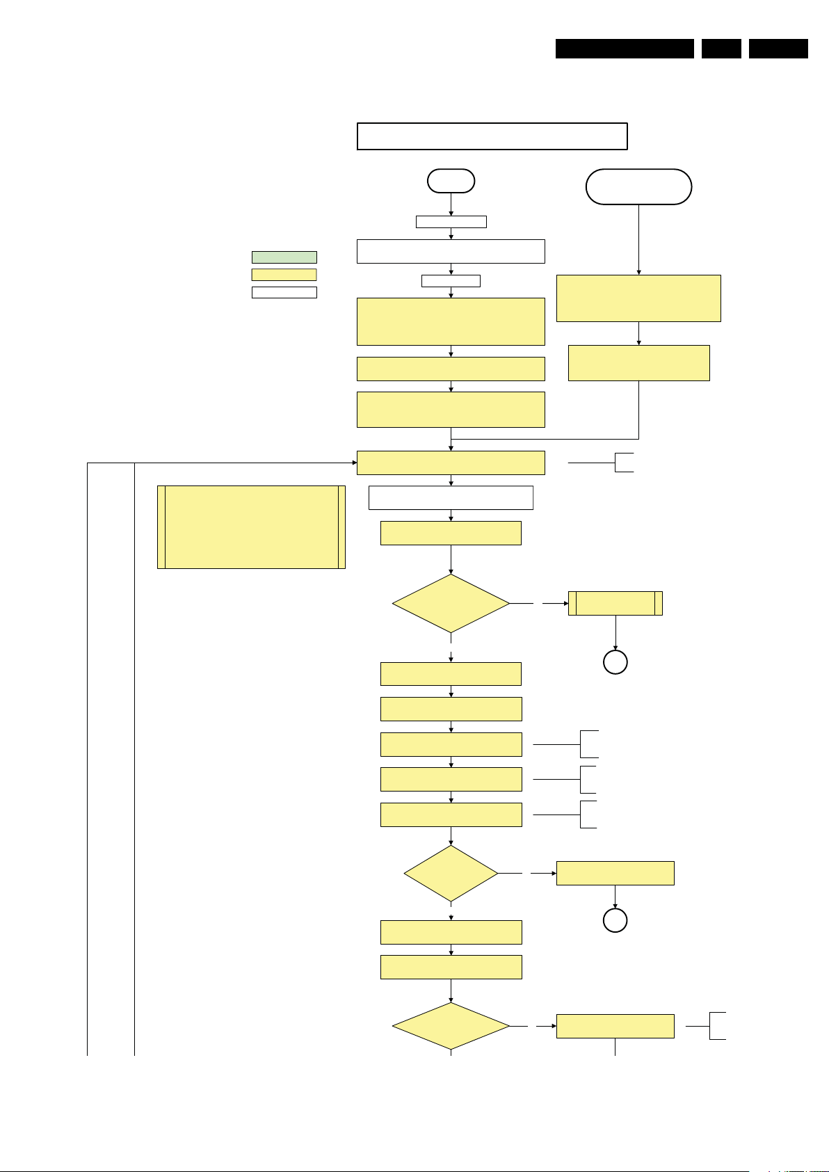
5.4 Stepwise Start-up
There are two possible situations: one for protections detected
by the stand-by software and one for protections detected by
the main software.
When the TV is in a protection state due to an error detected by
stand-by software (and thus blinking an error) and SDM is
activated via short-circuiting the pins on the SSB, the TV starts
up until it reaches the situation just before protection. So, this
is a kind of automatic stepwise start-up. In combination with the
start-up diagrams below, you can see which supplies are
present at a certain moment. Important to know is, that if e.g.
the 3V3 detection fails (and thus error 8 is blinking) and the TV
2009-Oct-16
Page 18
EN 18 PB52.1HU LC5.
Service Modes, Error Codes, and Fault Finding
Off
Mains
off
Mains
on
St by
(Off St by)
- POD Card removed
- tact SW pushed
On
For POD should be read Common Interface (CI)
- WakeUp
requested
- Acquisition
needed
- No data Acquisition
required
and no POD present
- tact SW pushed
- WakeUp
requested
- Acquisition
needed
No d ata
Acquisition
required and
POD pre sent
POD
St by
GoToProtection
Figure 5-2 Transition diagram
Semi
St by
GoToProtection
WakeUp
requeste
- St by
requested
- tact SW
pushed
WakeUp
requeste
d
d
Active
GoToProtection
Protection
H_17650_093.eps
180108
2009-Oct-16
Page 19
Service Modes, Error Codes, and Fault Finding
Off/Stby to Semi
EN 19PB52.1HU LC 5.
action holder: MIPS
action holder: St-by
autonomous action
The a vailability of th e supplie s is checked t hrough de tect
signals going to the st-by µP. These signals are available
for +12V and +5V (combined as AND function, called
detect-5V-12V) and for +1V2 and +3V3 (combined as
AND function, called detect-1V2-2V5-3V). A low to high
transition of the signals should occur within a certain time
after toggling the standby line. If an observer is detected
before the time-out elapses, of course, the process
should continue in order to minimize start up time.
Off
Mains is ap plied
Standby Supply starts running.
All stand by supply volta ges become a vailable .
st-b y µP resets
All I/O lines have a High default state:
- Switch PNX85xx in reset ( active LOW).
- NVM power line is high, no NVM communication possible.
Initialise I/O pins of the st-by µP, start keyboard scanning, RC
because of the stby µP r eset in an F HP set) which w ill start th e
Switch ON Platform and display supply by switching LOW the
- Keep the Audio-reset high.
detection. Wake up reasons are off.
PDPGO line is high (either HW wise in a non FHP set or
FHP PDP.
POD-MODE and the ON-MODE I/O lines.
+5V, and +12V are switched on
Wait 50ms and the n start pollin g the dete ct-
5V-12V every 40ms.
Stand by or
Protection
If the protection state was left by short circuiting the
SDM pins, detection of a protection condition during
startup will stall the startup. Protection conditions in a
playing se t will be ignor ed. Th e protect ion mode will
not be entered.
- Switch Audio-Reset high.
It is low in the standby mode if the standby
mode lasted longer than 10s.
Display sup ply is switched on
through the ON-mode I/O line
detect-5V-12V received within
2900 ms after POD-mode I/O
line tog gle?
Yes
activat e +5V/ +12V supply
detection algorithm. See CHS protections.
Enable the +1V2 supply (ENABLE-1V2 )
Wait 100m s
Enable the supply for
+1.8V and +3. 3V (ENABLE-3V3)
Start polling the detect-1V2-2V5-3V3
every 40ms
Detection
received within
250 ms after enable-3V3
toggle?
Yes
Activate supply detection algorithms for DC-
DC outputs
Wait 20ms
No
“5V 12V supply” error
SP
ms is recommended by the
100
spec
PNX
85xx
.
No separate enable is present
for the +1V8 supply in the
TV522.
Only one detect line is present
in the TV522: it detects +1V2
and +3V3
No
1V2 2V5 3V3 DCDC error
SP
SUPPLY-F AULT I/O line
is High ?
No
Figure 5-3 “Off” to “Semi Stand-by” flowchart (part 1)
Supply fault error
The supply fault line is an OR
function of DCDC, DCDC5050
and POD /CI supply sw itch.
H_17650_094a.eps
090826
2009-Oct-16
Page 20
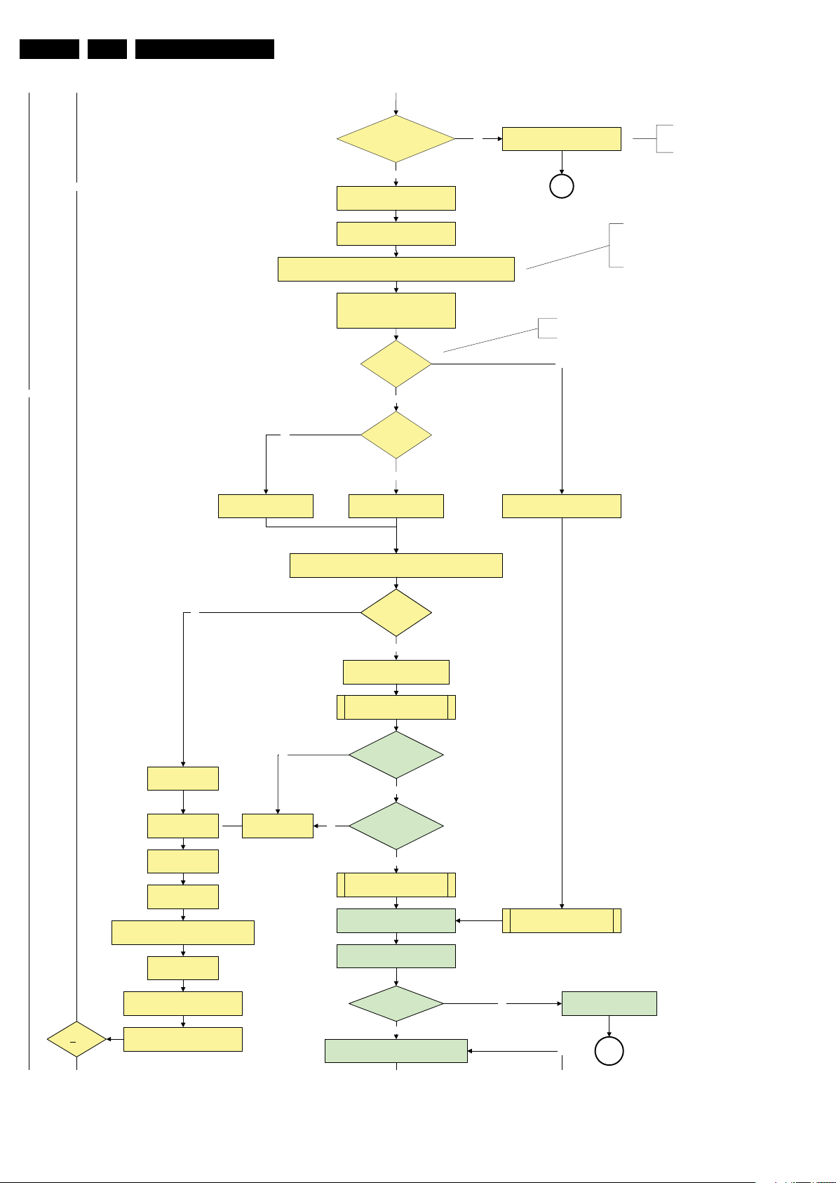
EN 20 PB52.1HU LC5.
Service Modes, Error Codes, and Fault Finding
SUPPLY-F AULT I/O line
is High ?
No
Switch LOW the RESET-NVM_WP-NANDFLASH line. Add a 2ms delay before
trying to address the NVM to allow correct NVM initialization.
No
No
Relea se AVC system r eset
Feed warm boot script
Enable the supply fault detection
(pulling pin of the probe interface to
ground by inserting EJTAG probe)
Yes
algorithm
Set I²C slave address
of Standby µP to (A0h)
Detect EJTAG debug probe
EJTAG probe
connected ?
No
Cold boot?
Yes
Relea se AVC system r eset
Feed cold boot script
No
Supply fault error
SP
This will a llow access to NVM and
NAND FLASH and can not be done
earlier because the FLASH needs to
be in Write Protect as long as the
supplies are not available.
An EJTAG probe (e.g. WindPower ICE probe) can
be connected for Linux Kernel debugging purposes.
Yes
Relea se AVC system r eset
Feed initializing boot script
disable alive mechanism
The supply fault line is an OR
function of DCDC, DCDC5050
and POD /CI supply sw itch.
No
Code = 5
Switch AVC PNX8 5xx
in re set (act ive low)
Wait 10ms
Switch the NVM r eset
line HIGH.
Disable all supply related protections and
switch off the +2V5, +3V3 DC/DC converter.
Wait 5ms
Boot process of the PNX5050 also starts at this point.
Bootscript ready
in 1250 ms?
Set I²C slave address
of Standby µP to (60h)
RPC start (comm. protocol)
No
Code = 53
Flash to Ram image
transfer succeeded
No
SW initializat ion
Enable Alive check mechanism
MIPS reads the wake up reason
from standby µP.
In case of an LCD set, check t he
Power- OK display line
Yes
within 30s?
Yes
succeeded
within 20s?
Yes
Wait until AVC starts to
commun icate
2009-Oct-16
3-th try?
switch off the remaining DC/DC
converters
Switch POD -MODE and ON- MODE
I/O line high.
Power-ok display high ?
Yes
Reset t he Pacific by pulling LOW the Pacific
hardware reset line during 100ms.
No
Figure 5-4 “Off” to “Semi Stand-by” flowchart (part 2)
Log power-ok error and enter
protection
No
MP
H_17650_094b.eps
090826
Page 21
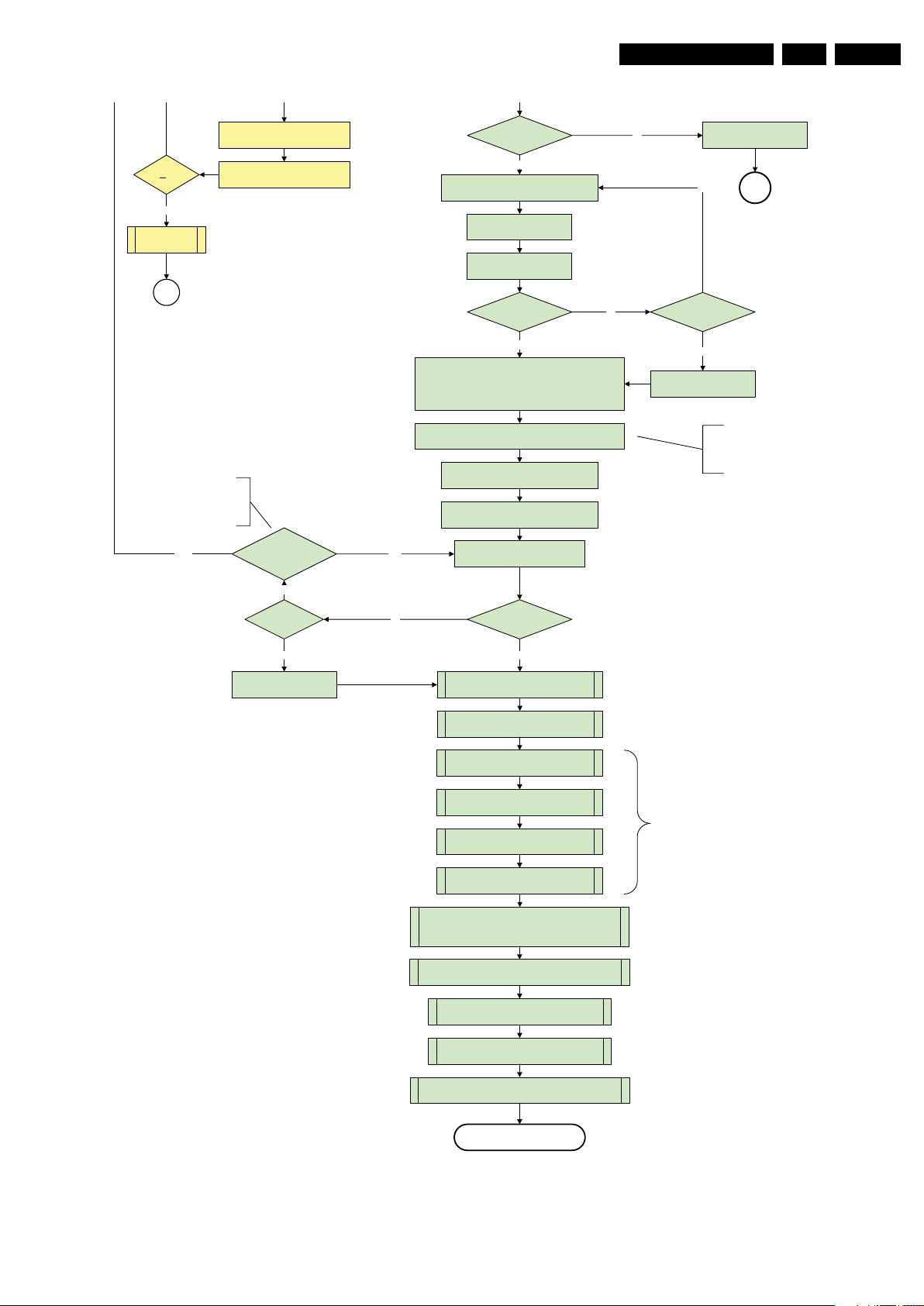
Service Modes, Error Codes, and Fault Finding
EN 21PB52.1HU LC 5.
switch off the remaining DC/D C
3-th try?
Yes
Blink Code as
error code
Switch POD -MODE and ON- MODE
SP
- Channeldecoder type TDA10060
cannot be reloaded without reset
of the channeldecoder.
- Channeldecoder type TDA10048
can be reloaded without reset.
conver ters
I/O line high.
Channel decoder
TDA 10048?
Power-ok display high ? No
Yes
Reset the Pacific by pulling LOW the Pacific
hardware reset line during 100ms.
Relea se Pacific rese t
and wait 200ms
Ping the Pacific through I²C
Pacific acknowledges?
Yes
Init Pa cific accordin g use case :
- lvds or CMOS input and output
- panel config…
to be discussed with Stefan / SW if we will put this here or in
the display excel overview of Stefan or in …..
Enable the Pacific output by sending the PanelConfig.PanelOn
YesNo
to the Pacific in case of a DFI set
Start 4 seconds preheating timer in case of
an LPL scann ing backlight LCD set.
Initialize audio accord ing FMS infor mation :
Download firmware into the channel
decoder
Log power-ok error and enter
protection
No
MP
Third Pacific boot retry?No
Yes
Log Pacific error
This is needed here because the Pacific has to
deliver an output clock towards the DFI. Otherwise
the DFI cannot deliver ambilight functionality in the
lampadaire mode. The presence of the DFI can be
determined via the display option.
No
Third try? No
Yes
Log channel decoder error
Downloaded
successfu lly?
Yes
initialize tuner , Master IF and channel
decoder
Initialize source selectio n
Wait until Cpipe delivers a stable output
Initialize video processin g IC 's :
- PNX5050 in /82
- scale r EPLD
initialize A utoT V by trigger ing CHS Aut oTV Init int erface
Initialize Pacific or EPLD related Ambilight
clock
Reset EPLD
Wait 100ms
Reset Pacific clock
settings (if applicable)
EPLD
and
Pacific
should
be reset
when a
stable
input
clock
become
s
available
at their
input.
Initialize Ambilight with Lights off.
Do not enter semi-standby state in case of an LPL
scanning backlight LCD set before 4s preheating timer has
elapsed.
Semi-Standby
Figure 5-5 “Off” to “Semi Stand-by” flowchart (part 3)
H_17650_094c.eps
090826
2009-Oct-16
Page 22
EN 22 PB52.1HU LC5.
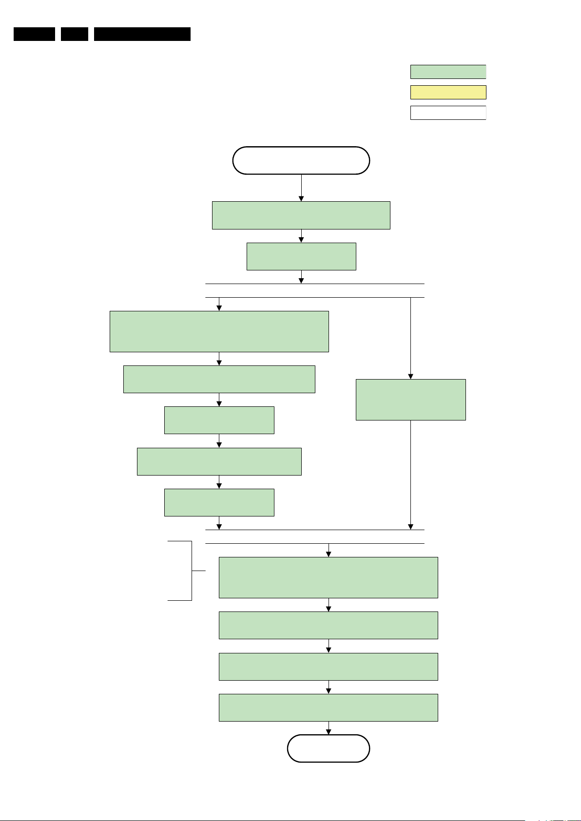
Service Modes, Error Codes, and Fault Finding
action holder: AVC
action holder: St-by
autonomous action
Semi Standby
Wait until previous on - state is left mor e than 2
seconds ago. (to prevent LCD display problems)
Assert RGB video blanking
and audio mute
Rewrite Pacific register 0x03 (output format) :
this command is sometimes not processed properly by the
Pacific at initialisation time , resending it here solves the issue .
Switch on the display by sending the
PanelConfig.PanelOn (I²C) command to the Pacific
wait 250ms (min. = 200ms)
Switch off the dimming backlight feature and
make sure PWM output is set to 100%
Switch on LCD backlight
The higher level requirement is that
audio and video should be demuted
without transient effects and that the
audio should be demuted maximum 1s
before or at the same time as the
unblanking of the video.
Initialize audio and video
processing IC's and functions
according needed use case.
Wait until valid and stable audio and video , corresponding to
the requested output is delivered by the AVC AND the
backlight PWM has been on for 1second.
2009-Oct-16
Switch Audio-Reset low and wait 5ms
Release audio mute and wait 100ms before any other audio
handling is done (e.g. volume change)
Restore dimming backlight feature, PWM output and unblank
the video.
Active
Figure 5-6 “Semi Stand-by” to “Active” flowchart
H_16770_110.eps
290307
Page 23
Service Modes, Error Codes, and Fault Finding
EN 23PB52.1HU LC 5.
Active
Mute all sound outputs via softmute
Wait 100ms
Set main amplifier mute (I/O: audio-mute)
Force ext audio outputs to ground
(I/O: audio reset)
And wait 5ms
switch off LCD backlight
action holder: AVC
action holder: St-by
autonomous action
Mute all video outputs
Wait 250ms (min. = 200ms)
Switch off the display by sending the
PanelConfig.PanelOff (I²C) command to the Pacific
switch off ambient light
Semi Standby
Figure 5-7 “Active” to “Semi Stand-by” flowchart
H_16770_112.eps
260307
2009-Oct-16
Page 24
EN 24 PB52.1HU LC5.
Service Modes, Error Codes, and Fault Finding
Semi Stand by
If ambientlight functionality was used in semi -standby
(lampadaire mode), switch off ambient light
Delay transition until ramping down of ambient light is
finished. *)
transfer Wake up reasons to the Stand by µP.
Switch Memories to self-refresh (this cr eates a more
stable condition when switching off the power).
Switch AVC system in reset state
action holder: MIPS
action holder: St-by
autonomous action
*) If this is not performed and the set is
switched to standby when the switch off of
the ambilights is still ongoing , the lights will
switch off abruptly when the supply is cut.
Import ant remark:
release reset audio 10 sec after
entering standby to save power
Wait 10ms
Switch the NVM reset line HIGH.
Disable all supply related protections and switch off
the +1V8 and the +3V3 DC/DC converter
Wait 5ms
switch off the +1V2 DC/DC converters
Switch OFF all supplies by switching HIGH the POD -
MODE and the ON-MODE I/O lines.
Stand by
For PDP this means
CPUGO becomes low.
H_16770_114.eps
260307
2009-Oct-16
Figure 5-8 “Semi Stand-by” to “Stand-by” flowchart
Page 25

Service Modes, Error Codes, and Fault Finding
EN 25PB52.1HU LC 5.
action holder: MIPS
action holder: St-by
autonomous action
MP
Log the appropriate error and
set stand-by flag in NVM
Redefine wake up reasons for protection
state and transfer to stand- by µP.
Switch off LCD lamp supply
Wait 250ms (min. = 200ms)
Switch off LVDS signal
Switch off 12V LCD supply within a time frame of
min. 0.5ms to max. 50ms after LVDS switch off.
SP
Ask stand-by µP to enter protection state
Switch AVC in reset stat e
Wait 10ms
Switch the NVM reset line HIGH.
Disable all supply related protections and switch off
the +1V8 and the +3V3 DC/DC converter.
Wait 5ms
switch off the +1V2 DC/DC converter
Switch OF F all supplies by sw itching HIGH the POD -
MODE and the ON-MODE I/O lines.
Flash the Protection-LED in order to indicate
protection state*.
Protection
Figure 5-9 “Protection” flowchart
(*): This can be the standby LED or the ON LED
depending on the availability in the set under
discussion .
H_16770_115.eps
290307
2009-Oct-16
Page 26

EN 26 PB52.1HU LC5.
Service Modes, Error Codes, and Fault Finding
5.5 Service Tools
5.5.1 ComPair
Introduction
ComPair (Computer Aided Repair) is a Service tool for Philips
Consumer Lifestyle products. and offers the following:
1. ComPair helps you to quickly get an understanding on how
to repair the chassis in a short and effective way.
2. ComPair allows very detailed diagnostics and is therefore
capable of accurately indicating problem areas. You do not
have to know anything about I
yourself, because ComPair takes care of this.
3. ComPair speeds up the repair time since it can
automatically communicate with the chassis (when the uP
is working) and all repair information is directly available.
4. ComPair features TV software up possibilities.
Specifications
ComPair consists of a Windows based fault finding program
and an interface box between PC and the (defective) product.
The (new) ComPair II interface box is connected to the PC via
an USB cable. For the TV chassis, the ComPair interface box
and the TV communicate via a bi-directional cable via the
service connector(s).
How to Connect
This is described in the ComPair chassis fault finding database.
TO
UART SERVICE
CONNECTOR
ComPair II
RC in
Optional
Switch
Power ModeLink/
Activity
RC out
2
C or UART commands
TO TV
TO
I2C SERVICE
CONNECTOR
Multi
function
UART SERVICE
CONNECTOR
2
C
I
TO
RS232 /UART
Note: If you encounter any problems, contact your local
support desk.
5.6 Error Codes
5.6.1 Introduction
The error code buffer contains all detected errors since the last
time the buffer was erased. The buffer is written from left to
right, new errors are logged at the left side, and all other errors
shift one position to the right.
When an error occurs, it is added to the list of errors, provided
the list is not full. When an error occurs and the error buffer is
full, then the new error is not added, and the error buffer stays
intact (history is maintained).
To prevent that an occasional error stays in the list forever, the
error is removed from the list after more than 50 hrs. of
operation.
When multiple errors occur (errors occurred within a short time
span), there is a high probability that there is some relation
between them.
Basically there are three kinds of errors:
• Errors detected by the Stand-by software. These errors
will always lead to protection and an automatic start of the
blinking LED for the concerned error (see paragraph “The
Blinking LED Procedure”). In these cases SDM can be
used to start up (see chapter “Stepwise Start-up”). Note
that it can take up to 90 seconds before the TV goes to
protection and starts blinking the error (e.g. error 53)
• Errors detected by main software that lead to
protection. In this case the TV will go to protection and the
front LED should also blink the concerned error. See also
paragraph “Error Codes” -> “Error Buffer” -> “Extra Info”.
For this chassis only error 63 is a protection error detected
by main software.
• Errors detected by main software that do not lead to
protection. In this case the error will be logged into the
error buffer and can be read out via ComPair, via blinking
LED method, or in case you have picture, via SAM.
PC
ComPair II Developed by Philips Brugge
Optional power
HDMI
2
I
C only
5V DC
Figure 5-10 ComPair II interface connection
Caution: It is compulsory to connect the TV to the PC as
shown in the picture above (with the ComPair interface in
between), as the ComPair interface acts as a level shifter. If
one connects the TV directly to the PC (via UART), ICs will be
blown!
How to Order
ComPair II order codes:
• ComPair II interface: 312278591020.
• See Philips Service website for latest software.
• ComPair RS232 cable: 310431112742 (to be used with
chassis Q52x).
2009-Oct-16
10000_036_090121.eps
090819
5.6.2 How to Read the Error Buffer
Use one of the following methods:
• On screen via the SAM (only if you have a picture). E.g.:
– 00 00 00 00 00: No errors detected
– 06 00 00 00 00: Error code 6 is the last and only
detected error
– 09 06 00 00 00: Error code 6 was first detected and
error code 9 is the last detected error
• Via the blinking LED procedure (when you have no
picture). See next paragraph.
•Via ComPair.
• Via CSM. when CSM is activated the blinking LED
procedure will start and the CSM content will be written to
a USB stick (if present).
5.6.3 How to Clear the Error Buffer
Use one of the following methods:
• By activation of the “RESET ERROR BUFFER” command
in the SAM menu.
• With a normal RC, key in sequence “MUTE” followed by
“062599” and “OK”.
• If the content of the error buffer has not changed for 50+
hours, it resets automatically.
5.6.4 Error Buffer
In case of non-intermittent faults, clear the error buffer before
you begin the repair (before clearing the buffer, write down the
content, as this history can give you significant information).
This to ensure that old error codes are no longer present.
Page 27
Service Modes, Error Codes, and Fault Finding
EN 27PB52.1HU LC 5.
If possible, check the entire contents of the error buffer. In
some situations, an error code is only the result of another error
code and not the actual cause (e.g., a fault in the protection
detection circuitry can also lead to a protection).
There are several mechanisms of error detection:
• Via error bits in the status registers of ICs.
• Via polling on I/O pins going to the stand-by processor.
• Via sensing of analogue values on the stand-by processor
or the PNX85xx.
• Via a “not acknowledge” of an I
2
C communication.
Take notice that some errors need more than 90 seconds
before they start blinking or before they will be logged. So in
case of problems wait 2 minutes from start-up onwards, and
then check if the front LED is blinking or if an error is logged.
Table 5-2 Error code overview
Error/
Error Description
3I2C3 E MIPS PNX85xx Error logged.
5 PNX85xx does
not boot (HW
cause)
6 5V, 12V supply P Stby P / Protection + Error
8 1V2, 1V4, 2V5,
3V3 supply
9 Supply fault P Stby P / Protection + Error
2
C-MUX1 E MIPS PCA9540 Error logged.
11 I
12 I2C-MUX2 E MIPS PCA9540 Error logged.
22 PNX5050 E MIPS PNX5050 Error logged.
23 HDMI mux E MIPS AD8190/
24 I2C switch E MIPS PCA9540 Error logged.
26 Master IF E MIPS TDA9898/
28 MOP (Ambilight
MOP on DFI
1)
panel)
34 Tuner E MIPS TD1716 Error logged.
37 Channel decoder E MIPS TDA10060/
38 MPEG4 E MIPS STi71xx Error logged.
46 Pacific3 E MIPS T6TF4 Error blinking + Error
53 PNX85xx does
not boot (SW
cause)
63 Power OK E/P MIPS / Error logged in case of
65 DFI (EPLD on
75 iBoard n.a. n.a. n.a. n.a.
76 Pro:Idiom n.a. n.a. n.a. n.a.
77 DMSD n.a. n.a. n.a. n.a.
DFI panel)
1)
Detected
Prot
by Device Result
E Stby P PNX85xx Error blinking.
blinking.
P Stby P / Protection + Error
AD8191
9897/9890
E MIPS EP2CXXF4
E Stby P PNX85xx Error blinking.
E MIPS / Error blinking + Error
84C7N
TDA10048
blinking.
blinking.
Error logged.
Error logged.
Error logged.
Error logged.
logged.
a PDP set. Protection
in case of an LCD set.
logged.
Note
1) Where applicable.
Extra Info
• Rebooting. When a TV is constantly rebooting due to
internal problems, most of the time no errors will be logged
or blinked. This rebooting can be recognized via a ComPair
interface and Hyperterminal (for Hyperterminal settings,
see paragraph “Stand-by software upgrade). You will see
that the loggings which are generated by the main software
keep continuing. In this case (rebooting) diagnose has to
be done via ComPair.
• Error 3 (I
2
C bus 3 blocked). At the time of release of this
manual, this error was not working as expected (error 3 is
logged and can be read out). Current situation: when this
error occurs, the TV will constantly reboot due to the
blocked bus. The best way for further diagnosis here, is to
use ComPair (e.g. read out the NVM content). Instead of
error “3” it is possible you will see error “2” in the error
buffer.
• Error 5 (PNX85xx doesn’t boot). Indicates that the main
processor was not able to read his bootscript. This error will
point to a hardware problem around the PNX85xx (supplies
not OK, PNX 8535 completely dead, I
and Stand-by Processor broken, etc...). When error 5
occurs it is also possible that I
2
I
C2 can be indicated in the schematics as follows: SCL-
2
C link between PNX
2
C2 bus is blocked (NVM).
UP-MIPS, SDA-UP-MIPS, SCL-SLAVE, SDA-SLAVE,
SCL-2 or SDA-2.
• Error 11 (I
2
I
C-MUX1 bus. At the time of release of this manual, this
2
C MUX1). Indicates a blocked (short circuited)
error was not working as expected. Current situation: when
this error occurs the TV will constantly reboot due to the
blocked bus. The best way for further diagnosis, is to use
ComPair (e.g. read out the NVM content).
• Error 12 (I
2
I
C-MUX2 bus. At the time of release of this manual, this
2
C MUX2). Indicates a blocked (short circuited)
error was not working as expected. Current situation: when
this error occurs the TV will constantly reboot due to the
blocked bus. The best way for further diagnosis, is to use
ComPair (e.g. read out the NVM content).
• Error 24 (I
2
C switch). As a side effect of error 24 it is
possible that error 47(no existing error) will also be logged.
• Error 28 (DFI Ambilight MOP). It can take up to 2 minutes
or more before this error is logged. So if you suspect that
this MOP is defective: clear the error buffer, restart the TV
and wait for about 2 minutes before checking the error
buffer.
• Error 37 (Channel decoder). When this error occurs,
there probably will be no picture and sound from tuner
input. As a side effect of error 37 it is possible that error 4
(no existing error) is also logged.
• Error 46 (Pacific 3). When there is an actual problem with
or around the Pacific during start-up, you will have no
picture and error 46 will be blinked via the blinking LED
procedure. For further diagnosis you can always dump the
CSM content on USB stick (see CSM) or use ComPair.
• Error 53. This error will indicate that the PNX85xx has read
his bootscript (if this would have failed, error 5 would blink)
but initialization was never completed because of hardware
problems (NAND flash, ...) or software initialization
problems. Possible cause could be that there is no valid
software loaded (try to upgrade to the latest main software
version). Note that it can take up to 2 minutes before the TV
starts blinking error 53.
• Error 63 (POWER OK). When this error occurs, it means
that the POWER-OK line did not became “high”. This error
is only applicable for TV’s with an LCD display. For PDP
displays there will be no protection during a POWER-OK
line failure, but error 63 will be logged in the error buffer.
Caution: in case a PDP TV ends up into power-ok
protection, it can indicate that the display option code is set
to “LCD”. To change the display option code to “PDP” you
need to activate SDM via the service pads (see figure
“Service mode pads”). Then change the display option
code blindly via a standard RC: key in the code “062598”
directly followed by the “MENU” button and “XXX” (where
XXX is the 3 digit decimal display option code as
mentioned in figure “Display option code overview”).
• Error 65 (DFI EPLD error). When this error occurs it
means that there is a problem with the I
2
C communication
towards the EPLD (picture processing EPLD, not the
Ambilight EPLD) on the DFI panel.
• Error 75 - 77. These errors are introduced specifically for
the iTV part of these sets.
2009-Oct-16
Page 28

EN 28 PB52.1HU LC5.
Service Modes, Error Codes, and Fault Finding
5.7 The Blinking LED Procedure
5.7.1 Introduction
The blinking LED procedure can be split up into two situations:
• In case of a protection. In this case the error is
automatically blinked. This will be only one error, namely
the one that is causing the protection. Therefore, you do
not have to do anything special, just read out the blinks. A
long blink indicates the decimal digit, a short blink indicates
the units.
• In the “on” state. Via this procedure, you can make the
contents of the error buffer visible via the front LED. This is
especially useful for fault finding, when there is no picture.
When the blinking LED procedure is activated in the “on” state,
the front LED will show (blink) the contents of the error-buffer.
Error-codes > 10 are shown as follows:
1. “n” long blinks (where “n” = 1 - 9) indicating decimal digit,
2. A pause of 1.5 s,
3. “n” short blinks (where “n”= 1 - 9),
4. A pause of approximately 3 s,
5. When all the error-codes are displayed, the sequence
finishes with a LED blink of 3 s,
6. The sequence starts again.
Example: Error 12 8 6 0 0.
After activation of the SDM, the front LED will show:
1. 1 long blink of 750 ms (which is an indication of the decimal
digit) followed by a pause of 1.5 s,
2. 2 short blinks of 250 ms followed by a pause of 3 s,
3. 8 short blinks followed by a pause of 3 s,
4. 6 short blinks followed by a pause of 3 s,
5. 1 long blink of 3 s to finish the sequence,
6. The sequence starts again.
Remark on the Supply Errors
The detection of a supply dip or supply loss during the normal
playing of the set does not lead to a protection, but to a cold
reboot of the set. If the supply is still missing after the reboot,
the TV will go to protection.
Protections during Start-up
During TV start-up, some voltages and IC observers are
actively monitored to be able to optimize the start-up speed,
and to assure good operation of all components. If these
monitors do not respond in a defined way, this indicates a
malfunction of the system and leads to a protection. As the
observers are only used during start-up, they are described in
the start-up flow in detail (see paragraph “Stepwise Start-up”).
5.8.2 Hardware Protections
The only real hardware protection in this chassis is (in case of
an audio problem) the audio protection circuit that will switch
“off” immediately the supply of the SSB. The supply will buzz
during the protection and +12VS drops to approximately 5V5
and +5V Stand-by to approximately to 1V9. Other indication of
the audio protection is that the red LED lights up with an
intensity of 50%.
Repair Tips
• It is also possible that you have an audio DC protection
because of an interruption in one or both speakers (the DC
voltage that is still on the circuit cannot disappear through
the speakers). Caution: (dis)connecting the speaker wires
during the ON state of the TV at high volume can damage
the audio amplifier.
5.7.2 How to Activate
Use one of the following methods:
• Activate the SDM or CSM. The blinking front LED will
show the entire contents of the error buffer (this works in
“normal operation” mode).
• Transmit the commands “MUTE” - “062500” - “OK”
with a normal RC. The complete error buffer is shown.
Take notice that it takes some seconds before the blinking
LED starts.
• Transmit the commands “MUTE” - “06250x” - “OK”
with a normal RC (where “x” is a number between 1 and
5). When x= 1 the last detected error is shown, x= 2 the
second last error, etc.... Take notice that it takes some
seconds before the blinking LED starts.
5.8 Protections
5.8.1 Software Protections
Most of the protections and errors use either the stand-by
microprocessor or the MIPS controller as detection device.
Since in these cases, checking of observers, polling of ADCs,
and filtering of input values are all heavily software based,
these protections are referred to as software protections.
There are several types of software related protections, solving
a variety of fault conditions:
• Protections related to supplies: check of the 12V, +5V,
+1V2, +1V4, 2V5 and +3V3.
• Protections related to breakdown of the safety check
mechanism. E.g. since the protection detections are done
by means of software, failing of the software will have to
initiate a protection mode since safety cannot be
guaranteed any more.
2009-Oct-16
Page 29

Service Modes, Error Codes, and Fault Finding
EN 29PB52.1HU LC 5.
5.9 Fault Finding and Repair Tips
Read also paragraph “Error Codes” -> “Error Buffer” -> “Extra
Info”.
5.9.1 Ambilight
Due to a degeneration process of the AmbiLight, it is
recommended to change all ambilight units in case one unit
needs to be repaired.
5.9.2 Audio Amplifier
It is recommended to replace all components at once (7D06,
7D09, 3D01, 3D25) when a defective FET 7D10 needs to be
fixed. For the left channel (defective FET 7D35) of the audio
amplifier replace all components like 7D31, 7D34, 3D11, 3D28.
5.9.3 CSM
When you activate CSM and there is a USB stick connected to
the TV, the software will dump the complete CSM content to the
USB stick. The file (Csm.txt) will be saved in the root of your
USB stick. If this mechanism works you can conclude that a
large part of the operating system is already working (MIPS,
USB...)
5.9.4 DC/DC Converter
Introduction
• The best way to find a failure in the DC-DC converters is to
check their starting-up sequence at “power-on via the
mains cord”, presuming that the standby microprocessor is
operational.
• If the input voltage of DC-DC converters is around 12.7V
(measured on decoupling capacitors (2U01 and 2U02) and
the enable signals are “low” (active), then the output
voltages should have their normal values. +12V and +5VPOD supplies start-up first (enabled by POD-MODE signal
from the standby microprocessor). There is a
supplementary condition for +12V to start-up: if +5V-POD
does not start up due to a local defect, then +12V will not
be available as well. +5V-ON supply is enabled by the ONMODE signal (coming also from the standby
microprocessor). +1V2 supply starts-up when +12V
appears, then at least 100 ms later, +1V8, +2V5 and +3V3
will be activated via the ENABLE-3V3 signal from the
standby microprocessor. If +12V value is less than 10 V
then the last enumerated voltages will not show-up due to
the under-voltage detection circuit 6U10 + 7U10 and
surrounding components. Furthermore, if +12V is less than
8V then also +1V2 will not be available. The third DC-DC
convertor that delivers +1V4 out of +12V is started up when
the ENABLE-1V2 becomes active (low) and +12V is
present.
• The consumption of controller IC 7U00 is around 19 mA
(that means almost 200 mV drop voltage across resistor
3U01) and the consumption of controller IC 7U64 is around
12 mA.
• The current capability of DC-DC converters is quite high
(short-circuit current is 7 to 10 A), therefore if there is a
linear integrated stabiliser that, for example, delivers 1.8V
from +3V3 with its output overloaded, the +3V3 stays
usually at its normal value even though the consumption
from +3V3 increases significantly.
• The +1V8 and +2V5 supply voltages are obtained via linear
stabilizer made with discrete components that can deliver
a lot of current, therefore in case +1V8 or +2V5 are shortcircuited to GND then +3V3 will not have the normal value
but much less.
• The SUPPLY-FAULT signal (active low) is an internal
protection (error 9) of the DC-DC convertor and will occur
if the output voltage of any DC-DC convertor is out of limits
(10% of the normal value).
Fault Finding
• Symptom: +1V2 not present (even for a short while ~10
ms)
1. Check 12 V availability (resistor 3U01, MOS-FETs
7U03 and 7U08), and +5V-POD.
2. Check the voltage on pin 9 (1.5 V),
3. Check for +1V2 output voltage short-circuit to GND that
can generate pulsed over-currents 7...10 A through coil
5U02.
4. Check the over-current detection circuit (2U20 or 3U40
interrupted).
• Symptom: +1V4 not present (even for a short while
~10ms) while +12V is okay (also across input capacitors
and ).
1. Check resistor and power MOS-FETs -1/2
2. Check the voltage on pin 4 (4 V)
3. Check enable signal ENABLE-1V2 (active “low”)
4. Check for +1V4 output voltage short-circuit to GND that
can generate pulsed over-currents 7...10 A through coil
5. Check the over-current detection reference( + ) and the
boot components ( + ).
• Symptom: +1V2 present for about 100ms, +1V8, +2V5
and +3V3 not rising.
1. Check the ENABLE-3V3 signal (active “low”),
2. Check the voltage on pin 8 (1.5 V),
3. Check the under-voltage detection circuit (the voltage
on collector of transistor 7U10-1 should be less than
0.8 V),
4. Check for output voltages short-circuits to GND (+3V3,
+2V5 and +1V8) that can generate pulsed overcurrents 7...10 A through coil 5U01,
5. Check the over-current detection circuit (2U18 or 3U31
interrupted).
• Symptom: +1V2 OK, +2V5 and +3V3 present for about
100 ms. Possible cause: SUPPLY-FAULT line stays “low”
even though the +3V3 and +1V2 is available - the standby
microprocessor is detecting that and switching “off” all
supply voltages.
1. Check the drop voltage across resistor 3U01 or 3U7B
(they could be too high, meaning a defective controller
IC or MOS-FETs),
2. Check if the boost voltage on pin 4 of controller IC
7U00 is less than 14 V (should be 19 V),
3. Check if +1V2 or +3V3 are higher than their normal
values - that can be due to defective DC feedback of
the respective DC-DC convertor (ex. 3U47, 3U77, or
3U70).
• Symptom: +1V2, +1V4, +1V8, +2V5 or +3V3 shows a high
level of ripple voltage (audible noise can come from the
filtering coils 5U01 or 5U02). Possible cause: instability of
the frequency and/or duty cycle of a DC-DC converter or
stabilizer.
1. Check the resistor 3U32 and 3U7B, capacitors 2U17
and 2U19, input and output decoupling capacitors.
2. Check a.c. feedback circuits
(2U23+2U24+3U55+3U63 for +1V2, and
2U07+2U08+3U17+3U24 for +3V3), compensation
capacitors 2U34, 2U36, 2U37, 2U40 and 2U68.
Note: when a pair of power MOSFETs (7U01+7U06 or
7U03+7U08) becomes defective the controller IC 7U00 should
be replaced as well.
5.9.5 Exit “Factory Mode”
When an “F” is displayed in the screen’s right corner, this
means that the set is in “Factory” mode, and it normally
happens after a new SSB has been mounted.
To exit this mode, push the “VOLUME minus” button on the
TV’s keyboard control for 5 seconds and restart the set.
2009-Oct-16
Page 30
EN 30 PB52.1HU LC5.
5.9.6 SSB Replacement
Follow the instructions in the flowchart in case you have to
exchange the SSB. See figure “SSB replacement flowchart”.
Instruction note: SSB replacement
Set is going into protection after
replacing the SSB
(blinking LED, error 2).
Take care that speakers are connected!
In some sets, the speakers are in the rear
cover, and when the set is switched “on”
without speakers, it is possible that the Audio
protection is triggered.
Advise: remount rear cover before switching
“on” (see also SCC_71772).
Service Modes, Error Codes, and Fault Finding
START
Set is still
operating?
Create “repair” directory on USB stick and
connect USB stick to TV-set
Go to SAM mode (062596 i+) and
save the TV settings via “Upload to USB”.
- Replace SSB board by a Service SSB.
- Make the SSB fit mechanically to the set.
Start-up set.
Set behaviour?
No
Set is starting up but no display.
Update main software in this step, by using
Program “Display Option” code via 062598
MENU/HOME, followed by 3 digits code (this
code can be found on a sticker inside the set).
After entering “Display Option” code, set is
going to Standby (= validation of code).
Connect PC via ComPair interface to Service
Program “set type number”, “serial number”,
“autorun.upg” file.
Restart the set.
No
connector.
Start TV in Jett mode (DVD i+/OSD)
Open ComPair browser
and “display 12NC”.
Set is starting up & display is OK.
Saved settings
on USB stick?
Yes
Go to SAM mode, and reload settings
via “Download from USB”.
Check latest software on Service website.
Update Main and Standby software via USB.
If not already done;
Check and perform alignments in SAM
according to the Service Manual.
E.g. option codes, colour temperature...
Set is starting up in “Factory” mode.
Noisy picture with bands/lines is visible and the
red LED is continuous “on”
(sometimes also the letter “F” is visible).
Press 5 s. the “Volume minus” button on the local
cntrl until the red LED switches “off”, and then
press 5 s. the MENU (*) button of the local cntrl.
(* in some chassis this button is named SOURCE)
The picture noise is replaced by blue mute!
Unplug the mainscord to verify the correct
disabling of the factory-mode.
Program “Display Option” code via 062598 MENU/
HOME, followed by 3 digits code (this code can be
found on a sticker inside the set).
After entering “Display Option” code, set is going
to Standby (= validation of code).
Restart the set.
In case of settings reloaded from USB, the set type,
serial number, Display 12NC, are automatically stored
when entering display options.
- Check if correct “Display Option” code is
programmed.
- Verify “Option Codes” according sticker inside the set.
- Default settings for White drive ...see Service Manual
2009-Oct-16
Final check of all menus in CSM.
Special attention for HDMI Keys.
END
Figure 5-11 SSB replacement flowchart
Q52xE SSB Board swap – v5.1
VDS/JA Updated 18-03-2009
(changes are indicated in red)
H_16771_007.eps
090828
Page 31

Service Modes, Error Codes, and Fault Finding
EN 31PB52.1HU LC 5.
5.9.7 Display option code
Caution: In case you have replaced the SSB, always check the
display option code in SAM, even if you have picture. With a
wrong display option code it is possible that you have picture,
but that in certain conditions you have unwanted side-effects.
5.9.8 Upgrade EDID NVM
To upgrade the EDID NVM you must short circuit pin 7 of the
EDID NVM to ground. Therefore some test points (EDID1 and
EDID2) are foreseen near the HDMI connectors, see ComPair
for further instructions.
5.10 Software Upgrading
5.10.1 WARNING - Flashing iBoard and/or NVM
When flashing iBoard and/or NVM, always check that you
have the correct software (PB52.1HU LA/B/C). No software
version check is implemented in this chassis. Accidental
software flashing from newer chassis/platforms will cause
the set to be inoperative!
Table 5-3 NAND-Flash content
5.10.2 Introduction
The set software and security keys are stored in a NANDFlash, which is connected to the PNX85xx via the PCI bus.
It is possible for the user to upgrade the main software via the
USB port. This allows replacement of a software image in a
stand alone set, without the need of an E-JTAG debugger. A
description on how to upgrade the main software can be found
in the DFU.
Important: When the NAND-Flash must be replaced, a new
SSB must be ordered, due to the presence of the security
keys!!! (copy protection keys, MAC address, ...).
Perform the following actions after SSB replacement:
1. Set the correct option codes (see sticker inside the TV).
2. Update the TV software (see the DFU for instructions).
3. Perform the alignments as described in chapter 8 (section
“Reset of Repaired SSB”).
4. Check in CSM if the HDMI keys are valid.
5.10.3 Main Software Upgrade
The software image resides in the NAND-Flash, and is
formatted in the following way, see table 5-3 NAND-Flash
content.
Nand Flash content FUS UPG Upgrade All UPG Flash Utils UPG
Partition Content erase program erase program erase program
JFFS2 partition 1 (application read write data) Channel table, EPG data x x x
JFFS2 partition 0 (Application read only once data) HDMI keys, back up display file x x
JFFS2 partition 0 (Application read only upgradeable data) wizard pictures, display file, cabinet file, upgrade assistant x x x
SQUASHFS partition Main software (MIPS) Linux structure (root file system) x x x x
BFFS partition 2 (DVD OK) Default software upgrade application TriMedia software boot batch
BFFS partition 1 (DVD cursor down) Back up software upgrade application boot batch file 1 Linux kernel
BFFS partition 0 Jaguar Boot loader boot batch file 0 xx
Block 0 BTM partition table x
• The above overview of the NAND Flash shows the content
of the different partitions. It also shows which part of the
one-zip file erases and programs which part of the NAND
Flash.
• Remark: the above does not mean that you can reprogram
your HDMI keys with the “UpgradeAll.upg” file from the one
zip file. This can only be done in a secure environment (e.g.
the factory).
• The “UpgradeAll.upg” file is only used in the factory.
• The “FlashUtils.upg” file is only used by service centers
file 2
JETT: needed for ComPair
Manual Software Upgrade
In case that the software upgrade application does not start
automatically, you can also start it manually.
How to start the software upgrade application manually:
1. Disconnect the TV from the Mains/AC Power.
2. Press the “OK” button on a Philips DVD RC-6 remote
control (it is also possible to use the TV remote in “DVD”
mode). Keep the “OK” button pressed while reconnecting
the TV to the Mains/AC Power.
3. The software upgrade application will start.
xx x x
xx xx
which are allowed to do component level repair on the
SSB.
Attention!
In case that you have started the download application
Automatic Software Upgrade
In “normal” conditions, so when there is no major problem with
the TV, the main software and the default software upgrade
application can be upgraded with the “AUTORUN.UPG” (FUS
part of the one-zip file: e.g. 3104 337 03801 _FUS _Q582E_
0.37.0.0_commercial.zip). This can also be done by the
consumers themselves, but they will have to get their software
from the commercial Philips website or via the Software Update
Assistant in the user menu (see DFU). The “autorun.upg” file
must be placed in the root of your USB stick.
How to upgrade:
manually, the “autorun.upg” will maybe not be recognized.
What to do in this case:
1. Create a directory “UPGRADES” on your USB stick.
2. Rename the “autorun.upg” to something else, e.g. to
“software.upg”. Do not use long or complicated names,
keep it simple. Make sure that “AUTORUN.UPG” is no
longer present in the root of your USB stick.
3. Copy the renamed “upg” file into this directory.
4. Insert USB stick in the side I/O.
5. The renamed “upg” file will be visible and selectable in the
upgrade application.
1. Copy “AUTORUN.UPG” to the root of your USB stick.
2. Insert USB stick in the side I/O while the set is in ON
MODE. The set will restart and the upgrading will start
automatically. As soon as the programming is finished, you
will get the message that you can remove your USB stick
and restart the set.
Back-up Software Upgrade Application
If the default software upgrade application does not start (could
be due to a corrupted boot 2 sector) via the above described
method, you can try to activate the “back-up software upgrade
application”.
2009-Oct-16
Page 32

EN 32 PB52.1HU LC5.
How to start the “back-up software upgrade application”
manually:
1. Disconnect the TV from the Mains/AC Power.
2. Press the “CURSOR DOWN” button on a Philips DVD RC6 remote control (it is also possible to use the TV remote in
“DVD” mode). Keep the “cursor down” button pressed
while reconnecting the TV to the Mains/AC Power.
3. The software upgrade application will start.
5.10.4 Stand-by Software Upgrade
There are two methods now to upgrade stand-by software:
Upgrade via USB
In this chassis it is possible to upgrade the Stand-by software
via a USB stick. The method is similar to upgrading the main
software via USB.
Use the following steps:
1. Create a directory “UPGRADES” on your USB stick.
2. Copy the Stand-by software (part of the one-zip file, e.g.
StandbySW_CFT01_9.0.0.0.upg) into this directory.
3. Insert the USB stick into the TV.
4. Start the download application manually (see paragraph
“Manual start of the Software Upgrade Application”.
5. Select the appropriate file and press the “red” button to
upgrade.
Service Modes, Error Codes, and Fault Finding
Upgrade via PC and ComPair interface
It will be possible to upgrade the Stand-by software via a PC
and the ComPair interface. Check paragraph “ComPair” on
how to connect the interface. To upgrade the Stand-by
software, use the following steps:
1. Disconnect the TV from the Mains/AC Power.
2. Short circuit the SPI pins [2] on the SSB (see figure
“Service mode pads” earlier in this chapter).
3. Keep the SPI pins shorted while connecting the TV to the
Mains/AC Power.
4. Release the short circuit after approximately two seconds.
5. Start up Hyper Terminal (can be found in every Windows
application via Programs -> Accessories ->
Communications -> Hyper Terminal). Use the following
settings:
–COM1
– Bits per second = 38400 (9600)*
– Data bits = 8
– Parity = none
– Stop bits = 1
– Flow control = None
6. Press “Shift U” on your PC keyboard. You should now see
the following info:
– PNX2015 Loader V1.0
– 19-09-2003
– DEVID=0x05
–Erasing
– MCSUM=0x0000
–=
7. If you do not see the above info, restart the above
procedure, and check your Hyper Terminal settings and
the connections between PC and TV.
8. Via “Transfer” -> “Send text file ...”, you can send the
proper upgrade file to the TV (e.g. *.hex).
9. After successful programming, you must see the following
info (this can take several minutes!):
– DCSUM=0xC67E
–:Ok
– MCSUM=0xC67E
– Programming
– PCSUM=0xC67E
– Finished
10. If you do not see this info, restart the complete procedure.
11. Close Hyper Terminal.
12. Disconnect and connect Mains/AC Power again.
(*) When having problems with upgrading, use the values
between brackets.
2009-Oct-16
Page 33

6. Alignments
Index of this chapter:
6.1 General Alignment Conditions
6.2 Hardware Alignments
6.3 Software Alignments
6.4 Option Settings
Note: The Service Default Mode (SDM) and Service Alignment
Mode (SAM) are described in chapter 5. Menu navigation is
done with the CURSOR UP, DOWN, LEFT or RIGHT keys of
the remote control transmitter.
Alignments
Description Test Point SupplyMin. Typ. Max.
+3V3-standby FU86 +3.15 +3.30 +3.45 DC-DC
+1V2-standby FU85 +1.20 +1.25 +1.30 DC-DC
+3V3-MP4 FAK5 +3.15 +3.30 +3.45 ST
+2V6-MP4 FAKC +2.50 +2.60 +2.70 ST
+1V1 FAK1 +1.05 +1.10 +1.15 ST
+12V1 F230 +11.40 +12.00 +12.60 I-board
6.3 Software Alignments
EN 33PB52.1HU LC 6.
6.1 General Alignment Conditions
Perform all electrical adjustments under the following
conditions:
• Power supply voltage (depends on region):
– AP-NTSC: 120 V
– AP-PAL-multi: 120 - 230 V
– EU: 230 V
AC
– LATAM-NTSC: 120 - 230 V
– US: 120 V
AC
or 230 VAC / 50 Hz (± 10%).
AC
/ 50 Hz (± 10%).
AC
/ 50 Hz (± 10%).
/ 50 Hz (± 10%).
AC
/ 60 Hz (± 10%).
• Connect the set to the mains via an isolation transformer
with low internal resistance.
• Allow the set to warm up for approximately 15 minutes.
• Measure voltages and waveforms in relation to correct
ground (e.g. measure audio signals in relation to
AUDIO_GND).
Caution: It is not allowed to use heatsinks as ground.
• Test probe: Ri > 10 Mohm, Ci < 20 pF.
• Use an isolated trimmer/screwdriver to perform
alignments.
6.1.1 Alignment Sequence
• First, set the correct options:
– In SAM, select “Options”, and then “Option numbers”.
– Fill in the option settings for “Group 1” and “Group 2”
according to the set sticker (see also paragraph
“Option Settings”).
– Press OK on the remote control before the cursor is
moved to the left.
– In submenu “Option numbers” select “Store” and press
OK on the RC.
OR:
– In main menu, select “Store” again and press OK on
the RC.
– Switch the set to Stand-by.
• Warming up (>15 minutes).
6.2 Hardware Alignments
There are no hardware alignments foreseen for this chassis,
but below find an overview of the most important DC voltages
on the SSB. These can be used for checking proper functioning
of the DC/DC converters, see table 6-1 SSB DC Voltages.
Table 6-1 SSB DC Voltages
Description Test Point SupplyMin. Typ. Max.
- Audio power FU15 -11.40 -12.00 -12.60 PSU
+ Audio power FU16 +11.40 +12.00 +12.60 PSU
+5V-standby FU18/FM25 +5.14 +5.20 +5.46 PSU
+12V FU19/FM26 +11.40 +12.00 +12.60 PSU
+1V2 FU06 +1.20 +1.25 +1.30 DC-DC
+3V3 FU07 +3.15 +3.30 +3.45 DC-DC
+1V8 IHZ3 t.b.d. +1.80 t.b.d. DC-DC
+5V-ON FU80 +4.95 +5.00 +5.30 DC-DC
+3V3-PI t.b.d. t.b.d. +3.30 t.b.d. Pro:idiom
Put the set in SAM mode (see Chapter 5 “Service Modes, Error
Codes and Fault Finding”). The SAM menu will now appear on
the screen. Select ALIGNMENTS and go to one of the sub
menus. The alignments are explained below.
The following item can be aligned:
• Whitepoint.
To store the data:
• Press OK on the RC before the cursor is moved to the left.
• In main menu select “Store” and press OK on the RC.
• Press MENU on the RC to switch back to the main menu.
• Switch the set to stand-by mode.
For the next alignments, supply the following test signals via a
video generator to the RF input:
• EU/AP-PAL models: a PAL B/G TV-signal with a signal
strength of at least 1 mV and a frequency of 475.25 MHz
• US/AP-NTSC models: an NTSC M/N TV-signal with a
signal strength of at least 1 mV and a frequency of 61.25
MHz (channel 3).
• LATAM models: an NTSC M TV-signal with a signal
strength of at least 1 mV and a frequency of 61.25 MHz
(channel 3).
• DVB-T models: see table “SDM default settings” in chapter
5.
6.3.1 White Point
• Set “Active control” to “Off”.
• Choose “TV menu”, “TV Settings” and then “Picture” and
put:
– “Dynamic contrast” to “Off”.
– “Color enhancement” to “Off”.
– “Light sensor” to “Off” where applicable.
– “Clear LCD” to “On” where applicable.
– “Brightness” to “50”.
– “Color” to “0”.
– “Contrast” to “100”.
• Go to the SAM and select “Alignments”-> “Whitepoint”.
White point alignment LCD screens:
• Use a 100% white screen as input signal and set the
following values:
– “Color temperature”: “Normal”.
– All “Whitepoint” values to: “127”.
– “Red BL offset” values to “8”.
– “Green BL offset” values to “8”.
In case you have a color analyzer:
• Measure with a calibrated (phosphor- independent) color
analyzer in the centre of the screen. Consequently, the
measurement needs to be done in a dark environment.
• Adjust the correct x,y coordinates (while holding one of the
White point registers R, G or B on 127) by means of
decreasing the value of one or two other white points to the
correct x,y coordinates (see table “White D alignment
values”). Tolerance: dx: ± 0.004, dy: ± 0.004.
2009-Oct-16
Page 34

EN 34 PB52.1HU LC6.
Alignments
• Repeat this step for the other color temperatures that need
to be aligned.
• When finished press OK on the RC and then press STORE
(in the SAM root menu) to store the aligned values to the
NVM.
• Restore the initial picture settings after the alignments.
Table 6-2 White D alignment values
Normal (9000
Value Cool (11000 K)
K) Warm (6500 K)
x 0.278 0.289 0.314
y 0.278 0.291 0.319
6.4 Option Settings
6.4.1 Introduction
The microprocessor communicates with a large number of I
ICs in the set. To ensure good communication and to make
digital diagnosis possible, the microprocessor has to know
which ICs to address. The presence / absence of these specific
ICs (or functions) is made known by the option codes.
Notes:
• After changing the option(s), save them by pressing the OK
button on the RC before the cursor is moved to the left,
select STORE in the SAM root menu and press OK on the
RC.
• The new option setting is only active after the TV is
switched “off” / “stand-by” and “on” again with the Mains
switch (the NVM is then read again).
6.4.2 Opt. No. (Option numbers)
Select this sub menu to set all options at once (expressed in
two long strings of numbers).
If you do not have a color analyzer, you can use the default
values. This is the next best solution. The default values are
average values coming from production (statistics).
• Select a COLOUR TEMPERATURE (e.g. COOL,
NORMAL, or WARM).
• Set the RED, GREEN and BLUE default values according
to the values in the “Tint settings” table.
• When finished press OK on the RC, then press STORE (in
the SAM root menu) to store the aligned values to the NVM.
• Restore the initial picture settings after the alignments.
Table 6-3 Tint settings
Colour Temp. R G B
Cool 122 120 121
Normal 125 118 108
Warm 127 110 75
An option number (or “option byte”) represents a number of
different options. When you change these numbers directly,
2
C
you can set all options very quickly. All options are controlled
via eight option numbers.
When the NVM is replaced, all options will require resetting. To
be certain that the factory settings are reproduced exactly, you
must set both option number lines. You can find the correct
option numbers on a sticker inside the TV set and in Table
“Option code overview”.
Example: The options sticker gives the following option
numbers:
• 57768 03076 08515 13923
• 59272 00068 00000 00000
The first line (group 1) indicates hardware options 1 to 4, the
second line (group 2) indicates software options 5 to 8.
Every 5-digit number represents 16 bits (so the maximum value
will be 65536 if all options are set).
When all the correct options are set, the sum of the decimal
values of each Option Byte (OB) will give the option number.
See tables “Option code overview” for the options.
6.4.3 Option Code Overview
Table 6-4 Option code overview
CTN 12NC Display type Display code
42HFL5440T/27 867000056444 LPL LC420WXE-SAA1 138 57768 03077 08519 46691 26506 00064 00000 00000
52HFL5480T/27 867000056445 LK520D3LA53 187 57770 03077 08519 46691 26555 00064 00000 00000
Important: after having edited the option numbers as
described above, you must press OK on the remote control
before the cursor is moved to the left!
Group 1 Group 2
OB1 OB2 OB3 OB4 OB5 OB6 OB7 OB8
2009-Oct-16
Page 35

7. Circuit Descriptions
Circuit Descriptions
EN 35PB52.1HU LC 7.
Index of this chapter:
7.1 Introduction
7.2 Main Supply
Notes:
•Only new circuits (circuits that are not published recently)
are described.
• Figures can deviate slightly from the actual situation, due
to different set executions.
• For a good understanding of the following circuit
descriptions, please use the wiring, block (chapter 6) and
circuit diagrams (chapter 7). Where necessary, you will find
a separate drawing for clarification.
7.1 Introduction
This chassis (member of the “TV522” platform) is a derivative
from the PB52.1HU LA chassis. It comes with the ME7 styling.
For a description of most circuitry, refer to the Q528.1E LA
Service Manual.
Important difference w.r.t. the previous PB52.1HU LA chassis
is the removal of the STi7101 MPEG4 PCMCIA decoder/
controller and Common Interface slot.
7.1.1 Features
The main features for this chassis are:
• The introduction of a module referred to as “Light Guide” on
the front side of the set (in some sets).
• Support of DVB-C reception (in some sets).
• For hospitality TV this chassis is provided with Pro:Idiom
technology.
• For all other features: refer to the Q528.1E LA/LB ans
PB52.1HU LA/LB Service Manual.
7.1.2 Service Attention Points
• One SSB version is to be used in different sets. So if a SSB
is installed in a TV-set, the technician has to make sure the
options are set correctly. Figure “SSB replacement
flowchart“ in chapter 5 describes the way to do a board
exchange.
• The ComPair connection to the set for this platform is made
to a headphone jack on the back of the sets which carry's
a RS232 level connection to communicate. For this, the in
chapter 5 paragraph “ComPair” mentioned RS232 cable is
needed.
• The repair workshop repairing the SSB's on component
level must load the latest set and NVM software in the SSB
before sending the boards back in the pool. This to make
sure that the board is working in a proper way when it is
mounted in a "to repair" set.
• In the CSM menu, the 12nc of the display will be
mentioned.
7.1.3 PB522 Architecture Overview
For details about the chassis block diagrams refer to chapter
“Block diagrams, Test Point Overview, and Waveforms”. An
overview of the PB522 architecture can be found in Figure 7-1
®
.
HDMI 1(rear)
HDMI 2(rear)
HDMI 3(MPEG4)
Hybrid Tuner
Saw
Decoder
TDA10060
PB Micro
UPSD3333D
ADI8191
HDMI
switch
Master IF
Pro:Idiom
LGDT1128
DDR-II
64MB
32
NXP
PNX8541
YUV20
BR/Pend
EPROM
32
EP2C8
ALT00
FPGA
FLASH
64MB
RGB30
Discreet
amp
Pac3
AmbiLight 2
PCI/XIO
USB2.0
Matrix
HD@60Hz
FHD@60H
z
Figure 7-1 Architecture of PB522 platform
18710_200_090825.eps
090826
2009-Oct-16
Page 36

EN 36 PB52.1HU LC7.
Circuit Descriptions
7.1.4 Pro:Idiom® Technology
This chassis is equipped with the second generation
Pro:Idiom
®
decryption device for the hospitality television
receiver market. The LGDT1128A/29 device family includes
enhanced electrostatic protection as well as adding MPEG 4
Receiver Block Diagram LGDT 1128A/29 Signal Description
•
Control Tuner for RF Channel Selection
•
Control Sub-Program selection in
multiplexed MPEG transport stream
Tuner Pro:Idiom
7.1.5 SSB Cell Layout
ATSC
Demodulator
Decryption
decrypting ability in the LGDT 1129 series. Pro:Idiom
leading content protection technology in the hospitality industry
and the LGDT 1128A/29 device family makes integration of this
technology into televisions and set top boxes simple and cost
efficient. This device is mounted on the SSB.
Conditional
Acces
I2C
Receiver
micro
MPEG
Decoder
Micro
Bus
Consumer
Remote
Control
Display
Figure 7-2 Architecture of Pro:Idiom
Inputs:
Data [7..0]
Start of Packet
Data Valid
TS Clock
Reset
I
LGDT
1128A/29
2
C[3..0]
27 MHz
®
is the
Outputs:
Data [7..0]
Start of Packet
Data Valid
TS Clock
I_17500_003.eps
170408
DC - DC CONVERSION
CLASS - D
SYSTEM INTERFACE
DDR2
SDRAM
DDR2
SDRAM
PNX8541
Pro:Idiom
DDR
SDRAM
STI7100
HDMI
SWITCH
DDR
SDRAM
2009-Oct-16
I_17500_071.eps
070408
Figure 7-3 SSB top view
Page 37

7.2 Main Supply
All sets in this chassis come with a buy-in Power Supply Unit
from the following suppliers:
• LG Philips for 42" sets
• Delta for 52" sets.
They are a black-box for Service. When defective, a new panel
must be ordered and the defective panel must be sent for
repair, unless the main fuse of the panel is broken. Always
replace a defective fuse with one with the correct
specifications! This part is available in the regular market.
See figure below for an overview of the PSU connectors for the
42" sets. These will make it easier to define if the PSU is
defective or not. In most cases the power supply voltages are
mentioned near the connectors on the power supply.
Circuit Descriptions
EN 37PB52.1HU LC 7.
CN1, CN9
Type : B2P-VA-BF(LF)(SN)
Maker : JST
CN4, CN5
Type : B4B-PH-K-S(LF)(SN)
Maker : JST
CN6
Type : B3B-PH-K-S(LF)(SN)
Maker : JST
SignalPin No.
NATURAL1
LIVE2
SignalPin No.
12V1
12V2
4
GND3
GND
SignalPin No.
12V1
NC2
GND3
Figure 7-4 PSU connector overview (for 42”)
CN10
Type : B2P-VA-BF(LF)(SN)
Maker : JST
CN7
Type : B9B-PH-K-S(LF)(SN)
Maker : JST
SignalPin No.
400Vdc1
GNDHOT2
SignalPin No.
(-)12V(audio)1
12V(audio)2
GND2(audio)3
5V24
5V25
5V26
GND7
GND8
GND9
CN2, CN3
Type : B03B-PASK-1(LF)(SN)
Maker : JST
CN8
Type : B8B-PH-K-S(LF)(SN)
Maker : JST
BL_ADJUST1
POWER_OK2
BL_ON/OFF3
STANDBY6
SignalPin No.
HV1
HV2
HV3
SignalPin No.
GND4
Boost5
5V27
12Vssb8
I_17951_014.eps
070808
2009-Oct-16
Page 38

EN 38 PB52.1HU LC8.
8. IC Data Sheets
This section shows the internal block diagrams and pin
configurations of ICs that are drawn as “black boxes” in the
electrical diagrams (with the exception of “memory” and “logic”
ICs).
8.1 Diagram B02A, LGDT1129 (IC 7B01)
Not available at time of issue.
8.2 Diagram B03, PNX85xx (IC 7H00)
Block Diagram
A/V INPUTS
VGA
HDMI
TDA10060
Channel
TD1736OF
Tuner
TDA9897
IF
IC Data Sheets
DDR-II
32 MB
PNX85xx
MIPS32@240MHz
TV control, Pixel OSD
Source select
3D-Comb
Digital color decoder
Audio decoding
Full audio processing, inc SRS
MPEG-2 HD/SD decode
MA DI
8-bit video processing
Enhanced PQ processing
Single LVDS output
HDMI / DVI
CA option
DDR-II
32 MB
16
16
LCD
Matrix Display
1368 × 768
SPDIF Out
TDA8933T
Audio Amp.
8/16
Pin Configuration
ball A1
index area
AB
AD
AF
AH
AK
USB2 Option
1 9 17 253 11 19 2771523513 21 29
A
B
C
D
E
F
G
H
J
K
L
M
N
P
R
T
U
V
W
Y
AA
AC
AE
AG
AJ
PNX85xx
Transparent top view
FLASH
16 MB
426121018 26412 22308 20 28614
H_16800_128.eps
230707
2009-Oct-16
Figure 8-1 Internal block diagram & pin configuration
Page 39

8.3 Diagram B05C, TPA4411RTJ (IC 7HV0)
(TOP VIEW)
IC Data Sheets
FunctionalPinning Block Diagram
EN 39PB52.1HU LC 8.
TPA4411
SVDD
_
+
SVSS
SVDD
+
_
SVSS
Av = −1.5 V/V
Short
Circuit
Protection
Charge
Pump
PVSS
C1P
PGND
C1N
NC
PVSS
SDL
PVDD
NC
20
19
18
1
2
3
4
5
8
7
6
NC
SVSSNCOUTL
NC − No internal connection
SGND
17
9
NC
16
10
SVDD
Audio In − R
INR
15
14
SDR
13
INL
12
NC
11
OUTR
SGND
Audio In − L
SDx
Bias
Circuitry
TERMINAL FUNCTIONS
TERMINAL
NAME QFN WCSP
C1P 1 A4 I/O Charge pump flying capacitor positive terminal
PGND 2 B4 I Power ground, connect to ground.
C1N 3 C4 I/O Charge pump flying capacitor negative terminal
NC B3, C3 No connection
4, 6, 8, 12,
16, 20
PVSS 5 D4 O Output from charge pump.
SVSS 7 D3 I Amplifier negative supply, connect to PVSS via star connection.
OUTL 9 D2 O Left audio channel output signal
SVDD 10 D1 I Amplifier positive supply, connect to PVDD via star connection.
OUTR 11 C2 O Right audio channel output signal
INL 13 C1 I Left audio channel input signal
SDR 14 B1 I Right channel shutdown, active low logic.
INR 15 A1 I Right audio channel input signal
SGND 17 A2 I Signal ground, connect to ground.
SDL 18 B2 I Left channel shutdown, active low logic.
PVDD 19 A3 I Supply voltage, connect to positive supply.
Exposed Pad -
I/O DESCRIPTION
(1)
Exposed pad must be soldered to a floating plane. Do NOT connect to power or
ground.
Audio Out − R
Audio Out − L
C1P
C1N
I_17500_004.eps
180408
Figure 8-2 Internal block diagram and pin configuration
2009-Oct-16
Page 40

EN 40 PB52.1HU LC8.
8.4 Diagram B06C, AD8197A (IC 7J00)
Block Diagram
IC Data Sheets
Pin Configuration
PP_OTO
100
1
AVCC
IN_B0
IP_B0
AVEE
IN_B1
IP_B1
VTTI
IN_B2
IP_B2
AVEE
IN_B3
IP_B3
AVCC
IN_A0
IP_A0
AVEE
IN_A1
IP_A1
VTTI
IN_A2
IP_A2
AVCC
IN_A3
IP_A3
AVEE
Figure 8-3 Internal block diagram and pin configuration
PIN 1 INDI CATOR
2
3
4
5
6
7
8
9
10
11
12
13
14
15
16
17
18
19
20
21
22
23
24
25
26
I2C_ADDR0
Figure 1.
TYPICAL APPLICATION
AUX_A2
AUX_A0
AUX_A1
AUX_A3
99
97
96
98
27
29
30
28
DVEE
I2C_ADDR2
I2C_ADDR1
AUX_B2
AUX_B0
AUX_B3
AUX_COM0
DVEE
AUX_B1
95
93
94
31
33
32
ON0
DVCC
PP_CH0
PP_CH1
AUX_COM1
89
92
91
90
AD8197
TOP VIEW
(Not to Scale)
37
34
35
36
OP1
OP0
ON1
VTTO
6471-001
04:20
AUX_COM2
AUX_COM3
AUX_C0
AUX_C3
AMUXVCC
AUX_C1
AUX_D0
AUX_D1
AUX_D2
AUX_D3
88
38
84
87
39
ON2
DVCC
82
86
40
OP2
81
85
83
42
45
44
41
43
OP3
ON3
VTTO
RESET
AUX_C2
PP_EQ
PP_EN
76
78
77
80
79
48
49
46
PP_PRE0
PP_PRE1
50
47
DVCC
PP_OCL
I2C_SCL
I2C_SDA
H_17650_080.eps
75
74
73
72
71
70
69
68
67
66
65
64
63
62
61
60
59
58
57
56
55
54
53
52
51
AVCC
IP_C3
IN_C3
AVEE
IP_C2
IN_C2
VTTI
IP_C1
IN_C1
AVEE
IP_C0
IN_C0
AVCC
IP_D3
IN_D3
AVEE
IP_D2
IN_D2
VTTI
IP_D1
IN_D1
AVCC
IP_D0
IN_D0
AVEE
150108
2009-Oct-16
Page 41

8.5 Diagram B10B, T6TF4HFG (IC 7GE2)
L
S
L
S
Block Diagram
2
SYNC
LVDS/CMOS RGB IN
Pat
gen
input
CMOS
30
LVDS
decoder
PLL1
Input Proc
MVL manager
Color gamut
mapping
Video Q meter
Noise estimator
Content
Detection
LVDS
decoder
PLL2
CLK_IN
32kB
16kB
256B
MRAM
60 MHZ RES
IC2_1
I2C_1
XRAM
IC2_2
ROM
I2C_3
I2C_2
Pin Configuration
JTAG
216
213
212
211
215
1
2
JTAG
3
4
5
6
7
8
9
10
11
12
13
14
15
16
17
-o input
18
19
20
VD
21
22
23
24
25
26
27
28
29
30
31
32
33
34
35
36
-e input
37
38
39
VD
40
41
42
43
44
45
46
47
48
49
R data input G data input B data input sync i
50
51
52
53
54
5556575859606162636465666768697071727374757677
208
210
209
214
207
Ambi-PWM LVDS-o output LVDS-e output
80C51
SPI
SI
SO
205
206
204
Control
Interrupt
reg. IF
CS
SCK
I2Cs0I2Cm
199
202
200
198
203
201
197
PACIFIC3-N2
IC Data Sheets
Contr, Brightness
&
White-point corr
Sharpness
Contr. enhance
H LTI
Histogram
Text enhance
Color processing
UART
contr
RSTN
INT_N
SPI
SPI 6 X GPIO PWM OSC
196
195
191
188
194
193
192
190
189
187
186
787980818283848586
B data outputA data output
Contrast Reserve
Clip Measure
& Dithering
Output buffering
AmbiLight
6
GPIO
I2Cs1
Interrupt test re set
182
185
179
183
181
184
180
178
878889909192939495
&
Color LUT
6
PWM
174
177
176
175
173
969798
99
C data output
inp_sync
Test
control
171
172
170
100
101
ADDR/DATA/RDN/WRN/
PSEN/TXD/RXD
T1
166
168
169
167
102
103
105
106
104
LVDS
LVDS
CMOS
Timing
control
Unit
PWM
BST
TDI
TCK
TDO
163
165
164
162
161
160
159
158
157
156
155
154
153
152
151
150
149
148
147
146
145
144
143
142
141
140
139
138
137
136
135
134
133
132
131
130
129
128
127
126
125
124
123
122
121
120
119
118
117
116
115
114
113
112
111
110
109
107
108
G_16840_099.eps
encoder
encoder
output
TMS
TRST
F data output
E data output
D data output
sync o
30
LVDS/CMOS R GB OUT
30
CMOS RGB OUT /
ND
P FLASH AND UART
2
CLK_OUT
3
SYNC
3
PWM
TRIGOUT
Proc data bus
UART
Proc address bus
clko
090207
EN 41PB52.1HU LC 8.
Figure 8-4 Internal block diagram and pin configuration
2009-Oct-16
Page 42

EN 42 PB52.1HU LC8.
/
IC Data Sheets
8.6 Diagram B12A, TDA1517ATW/N1 (IC 7111)
Not available at time of issue.
8.7 Diagram T01A, TDA10060 (IC7T18)
Block Diagram
PSC/SPI host
interface
interrupt
in-band tuner
in-band AGT
in-band AGI
in-band AFT
out-of-band tuner
out-of-band AGC
out-of-band VCO
PSC/SPI SLAVE
INTERFACE
IN-BAND AFE
PGA
12-bit A/D
AGC CONTROL
OUT-OF-BAND
AFE PGA
6-bit A/D
AGC CONTROL
VCO
OUT-OF-BAND
QPSK
RECEIVER
DVS-167 FEC
DVS-178 FEC
HAB
ATSC 8/16 VSB
ADVANCED
RECEIVER
ATSC 8/16 VSB
ADVANCED
RECEIVER
ACQUISITION
PROCESSOR
TDA10060
internal bus
to all blocks
ATSC FEC
ITU-T J.83
ANNEX
A/B/C FEC
MASTER
PLL
IN-BAND
OUTPUT
INTERFACE
OUT-OF-BAND
OUTPUT
INTERFACE
54 MHz
third overtone
crystal
MPEG
transport
out-of-band
transport
for CableCard
POD
Pin Configuration
PSC MASTER
INTERFACE
tuner/peripheral
control
GPIO/GPO
INTERFACE
GPIO GPO antenna
144
1
EIA/CEA-909
INTERFACE
control
109
108
TDA10060HL
36
37
Figure 8-5 Internal block diagram and pin configuration
73
72
JTAG
INTERFACE
JTAG
controller
H_16800_028.eps
111007
2009-Oct-16
Page 43

8.8 Diagram T01B, TDA9897HL (IC 7T57)
A
IC Data Sheets
EN 43PB52.1HU LC 8.
Block Diagram
4 MHz reference
input
(2)
R
EXTERNAL SOUND
FILTER
AM
BAND-PASS FILTER
+3 dB
FM CARRIER AGC
AM DEMODULATOR
FM NARROW-BAND PLL
35, 42
n.c.
SDA
SCL14i.c.
24
23
TDA9897
36
GCDIN
3
IF3A
4
IF3B
6
IF1A
7
IF1B
9
IF2A
10
IF2B
45
i.c.
TUNER
47
TAGC
48
GND
SIF AGC
PEAK
AGC
n.c.
I2C-BUS
VIF AGC
DECODER
2, 5, 18, 37
ADRSEL32BVS22GNDD
25
AM average
FM peak
2
C-BUS
I
TOPNEG
RSSI
DETECTOR
AND
IF BASED
TUNER
AGC
8
CTAGC
VIF PLL
AND
ACQUISITION
HELP
2
C-BUS TOP2
I
AND RSSI
optional tuner
AGC TOP for
IF based tuner
AGC and
radio signal
strength detector
onset
sideband
Q
I
sideband
I
Q
V
LFSYN2
1
SYNTHESIZER
AND VCO
A
A
B
B
TDA9897
C
GROUP
DELAY
1NYSFLFIVFL2POT
standard
C
D
D
E
E
F
F
G
G
H
H
SIDEBAND
FILTER
NYQUIST
FILTER
3111
SOUND
CARRIER
TRAP
trap reference
SYNTHESIZER
AND VCO
EQUALIZER
38
VIF
AFC
P
43, 44
SUPPLY
GNDA EXTFILO
40, 41 15
BAND-PASS
AND
(1)
EXTFILI
17
BP on/off
FM SWITCH
FM
AM
46 39
4 MHz FREQUENCY
SIF AGC
VIF AGC
19
LFFM
REFERENCE
OUTPUT
SWITCH
FM
AMPLIFIER
TAGC
FM AGC
AFC
2
C-bus
I
(2)
R
OPTXTALFREF
29
OUT2A
30
OUT2B
26
OUT1A
27
OUT1B
21
EXTFMI
CAF2
34
20
CDEEM
31
AUD
CAF1
28
16
MPP2
33
CVBS
12
port
MPP1
Pin Configuration
CIFAGC
LA
TX
ADNGMEE
CGAT.c
FERFOLIFTXE
DNGFIVFL
48
.c
P
.
i
VILI
4746454443
P
V.c
1
2
3
4
(1)
5
6
7
TDA9897HL
TDA9898HL
8
9
10
11
12
1314151617
.
i
18
2PPM
.
n
F
TXE
ADNGIM
.c.nMFFL
4140393837
42
202122
19
F
TXE
DC
T
P
OD
D
N
G
LFSYN1
n.c.
23
24
SCL
SDA
BVS
NIDCGA2NYSFL
.c.n.c.n
2FACA3FI
SBVCB3FI
DUAA1FI
B2TUOB1FI
A2TUOCGATC
1FACA2FI
B1TUOB2FI
A1TUO2POT
LESRDA1PPM
H_16800_029.eps
111007
36
35
34
33
32
31
30
29
28
27
26
25
Figure 8-6 Pin configuration
2009-Oct-16
Page 44

EN 44 PB52.1HU LC8.
IC Data Sheets
8.9 Diagram T01B, TD1736F/FHFXP (IC 7T57)
Block Diagram
RF input (F)
FM-trap
33V PLL
5V
RF out
5V Antenna power
2
1
4
AGC
5V
3
9
IIC bus
5
6
Pin Configuration
Terminal TD1736(O)F/FHFXP Remark
1 Antenna power option
2 RF Pin Output
3 External RF-gain control voltage (0.5V - 4.0V)
5 PLL chip address select (I
6 SCL (I
7 SDA (I
2
2
2
Max. permissible current:
100mA
Full band output
(53MHz - 865MHz)
(only available in “O” type)
Source impedance limited
to 1kohms
)renut / C
)renut / C
4MHz
7
8
11
seton noitacilppa eeS part MF 4
seton noitacilppa ees )renut / C
2009-Oct-16
tuptuo ecnerefeR zHM 4 8
9
+5V ± 5% supply voltage (V
TU
)
Tuner supply
dnuorG 01
delpuoc CA tuptuo - FI lacirtemmys-A 11
18710_300_090827.eps
Figure 8-7 Pin configuration
090827
Page 45

9. Block Diagrams
Wiring Diagram 42"
WIRING 42” (STYLING ME7)
Block Diagrams
8H18
CN6
1. +12VI
2. N.C.
3. GND
EN 45PB52.1HU LC 9.
LCD DISPLAY (1004)
LVD S INPUT
30P
2P3
BACKLIGHT
CN8
1. +12V(audio)
2. -12V(audio)
3. GND2(audio)
4. 5.2VS
5. 5.2VS
6. 5.2VS
7. GND1
CN3
3. V-LAMP
2. V-LAMP
1. V-LAMP
CN2
3. V-LAMP
2. V-LAMP
1. V-LAMP
MAIN POWER SUPPLY
IPB 42 PLHL-T605B
(1005)
CN1
2. L
1. N
8. GND1
9. GND1
CN7
1. BL_ADJUST
2. PG
3. BL_ON_OFF
4. GND1
5. BOOST
6. PS-ON
7. N.C
8. +12V
8308
8H20
8D00
1240 (B12B)
12. CVI_75R
11. Card_CVBS_out
10. POR1
9. SDA_I2C
8. GND
7. GND
6. +12VA
5. GND
4. RC_IN_MICRO
3. SPI_DATA_OUT
2. SPI_DATA_IN
1. SPI_CLK
1N30 (B08B)
4. GND
3. USB20-1-DP
2. USB20-1-DM
1. OUTB
1E91 (B07B)
5. FRONT_C
4. FRONT_Y_CVBS
3. GND
2. FRONT_AIN5-L
1. FRONT_AIN5-R
1230 (B12B)
3. GND
2. N.C.
1. +12VI
1E21 (B07A)
8. N.C.
7. Card_Aud_out_R
6. Card_Aud_out_L
5. GND
4. N.C.
3. CARD-PR
2. CARD-Y
1. CARD-PB
1D00 (B05A)
1. LEFT-SPEAKER
2. GND
3. GND
8H21
4. RIGHT-SPEAKER
TUNER
1U00 (B01A)
TUNER BOARD
T
1. -AUDIO-POWER
1C01 (B02A)
1T12 (T01A)
2. +AUDIO-POWER
3. GND
8. SCL-SSB-MUX2
8. SCL-SSB-MUX2
4. +5V-STANDBY
5. +5V-STANDBY
7. SDA-SSB-MUX2
6. +1V2
7. SDA-SSB-MUX2
6. +1V2
5. +1V2
8T02
5. +1V2
8D00
6. +5V-STANDBY
7. GND
8. GND
9. GND
4. GND
3. +3V3
2. GND
1. +12V
4. GND
3. +3V3
2. GND
1. +12V
1T13 (T01A)
20. GND
19. GND
18. RESET-SYSTEM-D
17. GND
16. SDA-SSB
15. SCL-SSB
14. GND
13. TUN-FE-ERR
.
.
1. TUN-FE-DATA7
1T11 (T01A)
5. IF-N
4. GND
3. IF-N
2. GND
1. CVBS-BO
INLET
1B28 (B09A)
1. BACKLIGHT-OUT
B
8T03
8G51
2. POWER-OK-DISPLAY
3. LAMP-ON-OUT
4. GND
5. BACKLIGHT-BOOST
SSB
(1150)
1C02 (B02A)
5. IF-N
4. GND
3. IF-N
2. GND
1. CVBS-BO
6. STANDBYn
7. +5V-STANDBY
8T01
8. +12V
1G50 (B10A)
1. SDA-I2C4-DISP
2. SCL-I2C4-DISP..
1C00 (B02A)
20. GND
19. GND
18. RESET-SYSTEM-D
17. GND
16. SDA-SSB
15. SCL-SSB
14. GND
13. TUN-FE-ERR
.
.
1. TUN-FE-DATA7
38. VDISP
1J40
20P
8M20
1N51 (B09E)
39. VDISP
40. VDISP
41. VDISP
1. LIGHT-SENSOR
2. GND
3. RC
4. LED2-OUT
5. +5V-STANDBY
6. LED1-OUT
7. KEBOARD
2P3
BACKLIGHT
KEYBOARD CONTROL
(1114)
1M01
3P
8M01
8T04
1J40
20P
HDMI BOARD
H
(1120)
RIGHT SPEAKER (5211)
1M207P1M01
+ -
+ -
LEFT SPEAKER (5212)
IR LED PANEL
(1112)
3P
18710_400_090824.eps
090826
2009-Oct-16
Page 46

Wiring Diagram 52"
WIRING 52” (STYLING ME7)
INVERTER
8317
CN2
14. PDIM_Select
13. PWM
12. On/Off
11. Vbri
8316
Block Diagrams
EN 46PB52.1HU LC 9.
LCD DISPLAY (1004)
LVD S INPUT
51P
8H18
CN8
1. +12VI
2. N.C.
3. GND
10. GND3
9. GND3
8. GND3
7. GND3
6. GND3
5. 24Vinv
4. 24Vinv
3. 24Vinv
2. 24Vinv
1. 24Vinv
7. GND3
6. GND3
5. 24Vinv
CN3
12. N.C.
11. N.C.
10. GND3
4. 24Vinv
9. GND3
8. GND 3
CN6
1. +12V(audio)
2. -12V(audio)
3. GND2(audio)
4. 5.2VS
5. 5.2VS
6. 5.2VS
7. GND1
8. GND1
9. GND1
CN7
1. BL_ADJUST
2. PG
3. BL_ON_OFF
4. GND1
5. BOOST
6. PS-ON
7. N.C
8. +12V
8H20
3. 24Vinv
2. 24Vinv
1. 24Vinv
8D00
8H21
8D00
8G51
8M20
14P 12P
MAIN POWER SUPPLY
PSU DPS-331AP2A B
(1005)
CN1
2. L
1. N
INLET
(B09A)
1B28
B
1. BACKLIGHT-OUT
8T03
3. LAMP-ON-OUT
4. GND
5. BACKLIGHT-BOOST
2. POWER-OK-DISPLAY
SSB
(1150)
1C02
5. IF-N
4. GND
3. IF-N
2. GND
1. CVBS-BO
6. STANDBYn
7. +5V-STANDBY
8T01
(B02A)
8. +12V
(B10A)
1. SDA-I2C4-DISP
1G50
2. SCL-I2C4-DISP
..38. VDISP
1C00
20. GND
19. GND
18. RESET-SYSTEM-D
17. GND
16. SDA-SSB
15. SCL-SSB
14. GND
13. TUN-FE-ERR
.
.
1. TUN-FE-DATA7
1J40
20P
39. VDISP
40. VDISP
(B02A)
3. GND
4. RIGHT-SPEAKER
TUNER
TUNER BOARD
T
(B01A)
1. -AUDIO-POWER
1U00
(B02A)
1C01
(T01A)
1T12
2. +AUDIO-POWER
3. GND
8. SCL-SSB-MUX2
8. SCL-SSB-MUX2
4. +5V-STANDBY
5. +5V-STANDBY
7. SDA-SSB-MUX2
6. +1V2
7. SDA-SSB-MUX2
6. +1V2
5. +1V2
8T02
5. +1V2
6. +5V-STANDBY
7. GND
8. GND
9. GND
4. GND
3. +3V3
2. GND
1. +12V
2. GND
1. +12V
4. GND
3. +3V3
1T13
(T01A)
20. GND
19. GND
18. RESET-SYSTEM-D
17. GND
16. SDA-SSB
15. SCL-SSB
14. GND
13. TUN-FE-ERR
.
.
1. TUN-FE-DATA7
1T11
(T01A)
5. IF-N
4. GND
3. IF-N
2. GND
1. CVBS-BO
(B05A)
2. GND
1. LEFT-SPEAKER
1D00
1240
(B12B)
12. CVI_75R
11. Card_CVBS_out
10. POR1
9. SDA_I2C
8. GND
7. GND
6. +12VA
5. GND
4. RC_IN_MICRO
3. SPI_DATA_OUT
2. SPI_DATA_IN
1. SPI_CLK
1N30
(B08B)
4. GND
3. USB20-1-DP
2. USB20-1-DM
1. OUTB
1E91
(B07B)
5. FRONT_C
4. FRONT_Y_CVBS
3. GND
2. FRONT_AIN5-L
1. FRONT_AIN5-R
1230
(B12B)
3. GND
2. N.C.
1. +12VI
1E21
(B07A)
8. N.C.
7. Card_Aud_out_R
6. Card_Aud_out_L
5. GND
4. N.C.
3. CARD-PR
2. CARD-Y
1. CARD-PB
8308
(B09E)
1N51
1. LIGHT-SENSOR
2. GND
3. RC
4. LED2-OUT
5. +5V-STANDBY
6. LED1-OUT
41. VDISP
8T04
1J40
20P
HDMI BOARD
H
(1120)
7. KEBOARD
KEYBOARD CONTROL
1M01
3P
(1114)
8M21
RIGHT SPEAKER
(5211)
1M207P1M01
+ -
+ -
LEFT SPEAKER
(5212)
IR LED PANEL
(1112)
3P
18710_401_090824.eps
090826
2009-Oct-16
Page 47

Block Diagram Video
VIDEO
MAIN TUNER
T01B
1T04
TD1736F/FHFXP
TUNER
VTU
CHANNNEL DECODER
T01A
MAIN
9
IF-OUT
ERF-GAIN
4-MHZ
FM-TRAP
V2
11
3
8
4
B06B
HDMI 1
CONNECTOR
HDMI 2
CONNECTOR
T0 3TH HDMI
HDMI BOARD
IF-OUT
7T56
1
19
1
19
ON
HDMI
18 2
18 2
1T06
1
SAW 45M75
1T55
1
SAW 44MHz
TUN-AGC
4-MHz
FM-TRAP-SWITCH
1JA0
1
ARX2+
3
ARX2-
4
ARX1+
6
ARX1-
7
ARX0+
9
ARX0-
10
ARXC+
12
ARXC-
13
15
16
19
ARX-HOTPLUG
1JB0
1
BRX2+
3
BRX2-
4
BRX1+
6
BRX1-
7
BRX0+
9
BRX0-
10
BRXC+
12
BRXC-
13
15
16
19
BRX-HOTPLUG
1J40
2
CRX2+
4
CRX2-
5
CRX1+
7
CRX1-
8
CRX0+
10
CRX0-
11
CRXC+
13
CRXC-
14
16
17
20
CRX-HOTPLUG
4
5
4
5
ARX-DCC-SCL
ARX-DCC-SDA
7JA2
BRX-DCC-SCL
BRX-DCC-SDA
7JB2
CRX-DCC-SCL
CRX-DCC-SDA
7J42
IF-FILTP1
IF-FILTN1
IF-FILTP3
IF-FILTN3
IF-OUT
TDA-IF-AGC
1T69
54M
CEC-HDMI
HOT-PLUG
CEC-HDMI
HOT-PLUG
CEC-HDMI
HOT-PLUG
B03B
(CONTROL)
B03G
(CONTROL)
B03B
(CONTROL)
B03G
(CONTROL)
B03B
(CONTROL)
B03G
(CONTROL)
7T57
TTDA9898HL/V2/S1
7
IF1-B
6
IF1-A
PROCESSING
3
IF3-A
4
IF3-B
10
IF2-B
47
TAG C
46
FREF
36
AGC-DIN
7T18
TDA10060HL
142
AGCT_CTL
115
GPIO-2
RECEIVER
21
XTAL-P
20
XTAL-N
B06C
B07C
B07A
B07B
1E90
2
N.C.
4
1E21
1
2
N.C.
3
B07B
1E91
4
N.C.
5
B12B
1240
11
N.C.
Block Diagrams
7T59
EF
CVBS-BO CVBS-BO
33
CVBS
IF
TDA-IF-IN-N
26
OUT1-A
OUT1-B
MPP-2
AGCT-CTL
GPIO-0
IF-N
IF-P
DTV
DATA
HDMI SWITCH
ARX2+
ARX2-
ARX1+
ARX1-
ARX0+
ARX0-
ARXC+
ARXC-
BRX2+
BRX2-
BRX1+
BRX1-
BRX0+
BRX0-
BRXC+
BRXC-
CRX2+
CRX2-
CRX1+
CRX1-
CRX0+
CRX0-
CRXC+
CRXC-
EXTERNAL VIDEO
ANALOGUE EXTERNALS
SIDE I/O
SIDE I/O
iBOARD
TDA-IF-IN-P
27
TUN-AGC-MON
16
7T06
141
3
8
7
40
TDA-IF-IN-N
TDA-IF-IN-P
RESET-SYS-DETECT
7J00
AD8191ASTZ
74
73
71
70
68
HDMI
67
SWITCH
65
64
12
11
9
8
6
5
3
2
62
61
59
58
56
55
53
52
TUN-FE-DATA(0-7) FE-DATA(0-7)
AV3
AV1
B03I
CARD_CVBS_out CVBS_MON_OUT
5HRR
3T59
3T58
34
OP0
33
ON0
37
OP1
36
ON1
40
OP2
39
ON2
43
OP3
42
ON3
44
10
5
1
VGA
CONNECTOR
PR
PB
Y
S VIDEO
AUDI O
EN 47PB52.1HU LC 9.
PRO: IDIOM
B02A
1C02
1T11
1
1
5
5
IF-N
IF-P
1002-2
1
2
15
3
13
6
11
14
1E30
1E10
1E12
1
3
5
4
2
3
1T13 1C00
1
13
18
7
4
1
2
3
5
1
3
1
TUN-FE-DATA(0-7)
13
18
B03C
(CONTROL)
RESET-SYS-DETECT
7005
1
4
5
8
FRONT_Y-CVBS
B03J
PNX85xx: ANALOGUE AV
7HUR
7HUX
RXC+
RX1+
RX2+
VGA_R
VGA_G
VGA_B
ITV-VGA-H
ITV-VGA-V
CVI-PR
CVI-PB
CVI-Y
AV1-CVBS
AV1- Y
AV1-C
CARD-PB
CARD-Y
CARD-PR
FRONT_C
CONTROL
7B01
LGDT1129
CONTROL
RXC-
RX0+
RX0-
RX1-
RX2-
B03C
(CONTROL)
IF-N
IF-P
B03
A10
A7
G2
R2
G1
H2
N4
K2
P2
7H00
PNX8541E
J3
M1
M2
A9
B7
B6
A8
B9
B8
K4
F3
T4
K3
R1
J1
P5
F2
J2
A3
PNX85xx
ANALOGUE AV
B03J
VIDEO
B03G
STREAMS
VIEDEO
STREAMS
ADC/MUX/SRC
B03G
PC_R
PC_G
PC_B
HSYNC_IN
VSYNC_IN
SWITCH/
VIDEO
STREAMS
HDMI
PNX85xx
MSP
VMPG
MPEG
DEMUX
AND
DECODING
VIDEC, 3D COMB AND VBI
CAPTURING
MAIN
VIDEO OUT
VIDEO
LAYER
GFX LAYER
STILL
MPEG/PC
CPIPE-TV
GFX OSD
LAYER
MBVP-TV
SNR/TNR
EDDI
HV SCALER
MEMORY
CONTROLLER
DIGITAL
B03H
VIDEO
OUT/LVDS
VID_OUT_TTL
LVD S
CONTROL
B03D
PCI XIO
SDRAM
B03E
DDR
AG15
AH15
AJ21
AK21
AJ22
AK22
AG22
AH22
AJ23
AK23
AG23
AH23
AJ24
AK24
B03F
TX8535oCLK-
TX8535oCLK+
B03F
PCI --> NAND
B03E
(0-12)
DDR2-D(0-15)
DDR2-A(0-12)
(16-31)
PNX85xx: DIGITAL
VIDEO OUT/LVDS
10 BIT YUV
DV-xx_Y(0-9)
DV-xx_UV(0-9)
DV-HS
DV-VS
TX8535oA-
TX8535oA+
TX8535oB-
TX8535oB+
TX8535oC-
TX8535oC+
TX8535oD-
TX8535oD+
TX8535oE-
TX8535oE+
PNX85xx: FLASH
7HA0
NAND512W3A2CN6E
NAND
FLASH
512Mx8
PNX 85xx: SDRAM
7HG0
EDE2516ACSE
DDR2
SDRAM
8Mx16x4
7HG1
EDE2516ACSE
DDR2
SDRAM
8Mx16x4
FPGA 1080P: I/0 BANKS
B09D
7F90
EP2C5F256C7N
CYCLONE II
FPGA
1080P
D13
D15
FPGA 1080p: INTERFACE
B09B
A7
B7
D6
C6
B6
A6
B5
A5
B4
A4
B3
A3
B14
A14
C13
C12
B13
A13
B12
A12
D11
D10
B10
A10
ONLY FOR 1080P SETS
9F35-9F46
TXFPGAeA-_G7
TXFPGAeA+_G6
TXFPGAeB-_G5
TXFPGAeB+_G4
TXFPGAeC-_G3
TXFPGAeC+_G2
TXFPGAeCLK+_G0
TXFPGAeCLK-_G1
TXFPGAeD-_R9
TXFPGAeD+_R8
TXFPGAeE-_R7
TXFPGAeE+_R6
TXFPGAoA-_B9
TXFPGAoA+_B8
TXFPGAoB-_B7
TXFPGAoB+_B6
TXFPGAoC-_B5
TXFPGAoC+_B4
TXFPGAoCLK+_B3
TXFPGAoCLK-_B2
TXFPGAoD-_B1
TXFPGAoD+_B0
TXFPGAoE-_G9
TXFPGAoE+_G8
RxP3eA-_G7
RxP3eA+_G6
RxP3eB-_G5
RxP3eB+_G4
RxP3eC-_G3
RxP3eC+_G2
RxP3eCLK+_G0
RxP3eCLK-_G1
RxP3eD-_R9
RxP3eD+_R8
RxP3eE-_R7
RxP3eE+_R6
RxP3oA-_B9
RxP3oA+_B8
RxP3oB-_B7
RxP3oB+_B6
RxP3oC-_B5
RxP3oC+_B4
RxP3oCLK+_B3
RxP3oCLK-_B2
RxP3oD-_B1
RxP3oD+_B0
RxP3oE-_G9
RxP3oE+_G8
FPGA BY-PASS
PACIFIC 3
B10C
7GE2
T6TF4HFG
28
29
31
32
34
35
38
39
PACIFIC3
40
ENHANCEMENT
41
44
45
9
10
13
14
15
16
19
20
22
23
25
26
PICTURE
75
74
78
77
81
80
84
83
87
86
90
89
93
92
96
95
99
98
101
100
103
102
107
106
B10A
DUAL LVDS ONLY1080P ONLY
TXECLK-
TXECLK+
TXOCLK-
TXOCLK+
7GE1
M25P05
512K
FLASH
TXEA-
TXEA+
TXEB-
TXEB+
TXEC-
TXEC+
TXED-
TXED+
TXEE-
TXEE+
TXOA-
TXOA+
TXOB-
TXOB+
TXOC-
TXOC+
TXOD-_
TXOD+
TXOE-
TXOE+
PACIFIC 3: LVDS
5G00
5G01
5G02
5G03
5G04
5G05
5G06
5G07
5G08
5G09
5G10
5G11
1G50
32
31
30
29
28
27
25
24
22
21
20
LVD S
19
CONNECTOR
TO DISPLAY
17
16
15
14
13
12
10
9
7
6
5
4
18710_402_090824.eps
090825
2009-Oct-16
Page 48

Block Diagram Audio
AUDIO
MAIN TUNER
T01B
1T04
TD1736F/FHFXP
MAIN
TUNER
VTU
CHANNNEL DECODER
T01A
9
IF-OUT
ERF-GAIN
4-MHZ
FM-TRAP
V2
11
3
8
4
B06B
1
19
HDMI 1
CONNECTOR
1
19
HDMI 2
CONNECTOR
T0 3TH HDMI
ON
HDMI BOARD
IF-OUT
7T56
HDMI
18 2
18 2
1T06
1
SAW 45M75
1T55
1
SAW 44MHz
TUN-AGC
4-MHz
FM-TRAP-SWITCH
1JA0
1
ARX2+
3
ARX2-
4
ARX1+
6
ARX1-
7
ARX0+
9
ARX0-
10
ARXC+
12
ARXC-
13
15
16
19
ARX-HOTPLUG
1JB0
1
BRX2+
3
BRX2-
4
BRX1+
6
BRX1-
7
BRX0+
9
BRX0-
10
BRXC+
12
BRXC-
13
15
16
19
BRX-HOTPLUG
1J40
2
CRX2+
4
CRX25
7
CRX18
CRX0+
10
CRX0-
11
CRXC+
13
CRXC-
14
16
17
20
CRX-HOTPLUG
4
5
4
5
ARX-DCC-SCL
ARX-DCC-SDA
7JA2
BRX-DCC-SCL
BRX-DCC-SDA
7JB2
CRX-DCC-SCL
CRX-DCC-SDA
7J42
IF-FILTP1
IF-FILTN1
IF-FILTP3
IF-FILTN3
IF-OUT
TDA-IF-AGC
1T69
54M
CEC-HDMI
HOT-PLUG
CEC-HDMI
HOT-PLUG
CEC-HDMI
HOT-PLUG
B03B
(CONTROL)
B03G
(CONTROL)
B03B
(CONTROL)
B03G
(CONTROL)
B03B
(CONTROL)
B03G
(CONTROL)
7T57
TTDA9898HL/V2/S1
7
IF1-B
6
IF1-A
PROCESSING
3
IF3-A
4
IF3-B
10
IF2-B
47
TAG C
46
FREF
36
AGC-DIN
7T18
TDA10060HL
142
AGCT_CTL
115
GPIO-2
RECEIVER
21
XTAL-P
20
XTAL-N
B06C
B03I
B07A
B07B
1E90
6
N.C.
8
1E21
6
N.C.
7
B07B
1E91
2
N.C.
1
Block Diagrams
7T59
33
CVBS
IF
26
OUT1-A
27
OUT1-B
MPP-2
AGCT-CTL
GPIO-0
DTV
TUN-AGC-MON
16
7T06
141
3
8
IF-N
7
IF-P
DATA
40
HDMI SWITCH
ARX2+
ARX2-
ARX1+
ARX1-
ARX0+
ARX0-
ARXC+
ARXC-
BRX2+
BRX2-
BRX1+
BRX1-
BRX0+
BRX0-
BRXC+
BRXC-
CRX2+
CRX2-
CRX1+
CRX1-
CRX0+
CRX0-
CRXC+
CRXC-
AUDI O
ANALOGUE EXTERNALS
SIDE I/O
B03I
SIDE I/O
PRO: IDIOM
B02A
1C02
IF-N
IF-P
VGA-AIN4-L
VGA-AIN4-R
AUDIO-IN1-L
AUDIO-IN1-R
CVI-AIN3-L
CVI-AIN3-R
CONTROL
FRONT-AIN5-L
FRONT-AIN5-R
1T11
1
1
5
5
3
3
1T13 1C00
1
1
TUN-FE-DATA(0-7)
13
13
18
18
B03C
(CONTROL)
RESET-SYS-DETECT
SPDIF
B06A
A-PLOP
7J50
4
B05C
(AUDIO)
&
SPI-OUT SPDIF-OUT
Audio-out-L
Audio-out-R
EF
CVBS-BO CVBS-BO
TDA-IF-IN-N
TDA-IF-IN-P
TDA-IF-IN-N
TDA-IF-IN-P
RESET-SYS-DETECT
7J00
AD8191ASTZ
74
73
71
70
68
67
SWITCH
65
64
12
11
9
8
6
5
3
2
62
61
59
58
56
55
53
52
PC
AUDIO IN
L+R
AV1
AUDIO IN
L+R
AV3
DIGITAL
AUDIO OUT
3T59
3T58
TUN-FE-DATA(0-7) FE-DATA(0-7)
HDMI
34
OP0
33
ON0
37
OP1
36
ON1
40
OP2
39
ON2
43
OP3
42
ON3
44
1126
2
3
5
1
1E10
2
3
5
1
1E30
9
6
+
3
AUDI O
Card_Aud_out_L
Card_Aud_out_R
5HRS
5HRT
7B01
LGDT1129
CONTROL
RXC+
RXC-
RX0+
RX0-
RX1+
RX1-
RX2+
RX2-
B03C
(CONTROL)
1
2
7HMD
IF-N
IF-P
ADAC(7)
ADAC(8)
B03
M1
M2
A10
A9
B7
B6
A8
A7
B9
B8
AK5
AH4
AJ6
AK6
AH5
AJ5
AJ15
AG8
AG7
AJ4
AK4
EN 48PB52.1HU LC 9.
7H00
PNX8541E
B03J
J3
B03G
B03G
B03G
PNX85xx
ANALOGUE AV
VIDEO
STREAMS
B03I
VIDEO
STREAMS
HDMI
VIDEO
STREAMS
AUDIO
PNX85xx
SPDIF DECODING,
MULTICHANNEL,
DOWNMIX AND SRC
ADC
SPDIF OUT
DELAYED
DEMDEC
MEMORY
CONTROL
B03H
B03B
CONTROL
B03D
PCI XIO
SDRAM
B03E
DDR
AUDIO
B03I
EPICS
DIGITAL VIDEO
OUT / LVDS
STANDBY
CONTROLLER
DAC
DAC
DAC
AJ13
AK12
AH16
V4
AH11
AH10
B03F
PCI --> NAND
B03E
DDR2-D(0-15)
DDR2-A(0-12)
(16-31)
B03I
ADAC(1)
ADAC(2)
ADAC(3)
ADAC(4)
PNX85xx: FLASH
7HA0
NAND512W3A2CN6E
NAND
FLASH
512Mx8
PNX85xx: SDRAM
7HG0
EDE2516AEBG
(0-12)
7HG1
EDE2516AEBG
PNX85xx:
AUDI O
(AUDIO)
DDR
SDRAM 1
8Mx16x4
DDR
SDRAM 2
8Mx16x4
9HM1
9HM2
B03I
AUDIO LEFT / RIGHT
B05A
+AUDIO-L
FEEDBACK
-AUDIO-R
FEEDBACK
AUDIO: PROTECTION / MUTE CONTROL
B05B
PNX85xx: STANDBY CONTROLLER
B03B
AUDIO HEADPHONE
B05C
B12A
A-PLOP
A-PLOP-HDPH
IBOARD
7111
TDA1517ATW/N1
3
18
AMPLIFIER
7HVA
7HV1
POWER
7D00-2
11
7D00-3
5
MUTE
MUTE
DV-B3_AUDIO-MUTE
AUDIO-RESET
AUDIO-RESET
7HV0
TPA4411RTJ
18
HEADPHONE
13
15
8
(CONTROL)
9
DRIVER
B12B
13
2
PEND_IR
DC_BST
MPEG4_PWR
7D63÷7D64
CONTROL
B07B
9
11
+AUDIO-POWER
7D10-1
7D10-2
CONTROL
-AUDIO-POWER
+AUDIO-POWER
7D35-1
7D35-2
CONTROL
-AUDIO-POWER
SIDE I/O
AUDIO-HDPH-L-AP
AUDIO-HDPH-R-AP
4120
CONTROL
5D00 5D10
5DO7
DC-SENCE
6HW0
6HW1
1122
3
2
5
4
1
5D11
AUDIO-MUTE
1E90
10
11
7
LEFT-SPEAKER
FEEDBACK-LR
RIGHT-SPEAKER
FEEDBACK-RL
7D00-1
8
7D00-4
7
N.C.
EXTERNAL
LOUDSPEAKER
1D00
1
2
Speaker L
3
4
Speaker R
7D70
14
AUDIO-PROT
CONTROL
1
B01A
18710_403_090824.eps
090825
2009-Oct-16
Page 49

Block Diagram Control & Clock Signals
CONTROL + CLOCK SIGNALS
B09A
SUPPLY
1B28
1
2
3
TO
5
POWER
SUPPLY
6
7
8
B08B
USB 2.0
N.C.
4 3 21
USB 2.0
CONNECTOR
B09C
FPGA 1080P: POW + CONTR
B09E
IR LED
BACKLIGHT-OUT
POWER-OK-DISPLAY
LAMP-ON-OUT
BACKLIGHT-BOOST
STANDBYn
+5V_STANDBY
+12V
1N30
1
2
3
4
5
8
1N31
1
2
3
4
7FA3
EPCS1SI8N
SCD
B10B
B03B
B10B
B10B
B01B
7N30
RYC8620
OUTB
OUTA
TO IR/LED PANEL AND
KEYBOARD CONTROL
B12A
(AUDIO)
B09E
1
2
3
4
6
2
DCLK
B12B
PEND_IR
RC
SYSTEM INTERFACE
(OPTIONAL)
B08A
B03C
B09D
DATA0
IBOARD
TO
USB 2.0
USB20-2-DM
USB20-2-DP
USB20-PWE1
USB20-OC1
USB20-OC2
USB20-PWE2
PCI-CLK-USB20
USB20-1-DM
USB20-1-DP
RESET-SYS-DETECT
FPGA 1080P: I/O BANKS
7F90
EP2C5F256C7N
H4
CYCLONE II
F1
1080P
FPGA
1N51
7
6
4
3
5
1
&
1240
2
4
10
LED1-OUT
LED2-OUT
+5V_STANDBY
Block Diagrams
RJ12
SMARTPLUG
B12A
B12A
IR-out-iB
B09E
B09E
B09E
B12B
TV-POR
B12B
7262
RC_IN_MICRO
7261
SPI_DATA_IN
7N00
ISP1564HL
90
PCI
92
HOST
CONTROLLER
79
78
87
88
7
83
85
5
B04E
PCI-CLK-PNX5050_CLK-MOP
J2
DV-CLK
H16
DV-CLK-PLL
E14
N9
H2
RC
IR-out-iB
LIGHT-SENSOR
1250
1
2
3
4
5
6
MUTE_iB
MPEG4_PWR
LED1-OUT
LED2-OUT
POR
IR_OUT
KEYBOARD
B12B
B12B
B12B
1240-1
SPI_CLK
IR-IN_DATA_IN_RXD_SDA1
GND
SPI_DATA_OUT
GND
IR_OUT
7220
UPSD3333D
51
52
49
MCU
1
28
44
40
26
25
CONTROL
B12A
B12B
75
74
9
8
1N01
B12B
12M
B03D
PNX8541: CONTROL
B03B
PNX 85xx: STANDBY CONTROLLER
+3V3-STANDBY
B03C
B03B
B03B
B06B
B03C
B08A
B08A
B08A
B08A
B12B
B12B
B06B
46
48
34
LED1-3V3
LED2-3V3
35
31
24M
1205
32
IR-IN_DATA_IN_RXD_SDA1
IBOARD
POR1
POR
TV_POR
PCI-AD(0-31)
PCI-GNT-USB20
7HD0
NCP303LSN
RST
2
IN
3
GND
DETECT-1V2-2V5-3V3
RESET-SYS-DETECT
CTRL4-STBY_SELECT-PWM-ANA
CTRL3-STBY_POWER-OK-DISP
LED1-3V3
LED2-3V3
HOT-PLUG
6253
B03B
B03B
F101
F102
POWER
CONTROL
ON RESET
PCI-REQ-USB20
1
RESET-STBY
DETECT-5V-12V
CEC-HDMI
AV1-BLK
AV2-BLK
KEYBOARD
LIGHT-SENSOR
EN 49PB52.1HU LC 9.
B03
PNX85xx
7H00
PNX8541E
D10
VIDEO STREAMS
B03G
PNX85xx
SDRAM
B03E
CONTROL
B03D
B12B
IBOARD
B03C
B03A
B03H
CONTROL
POWER
DIGITAL
VIDEO
OUT/LVDS
CONTROL
B03D
E22
E20
STANDBY CONTROLLER
B03B
AA3
DIGITAL
B03H
AK17
VIDEO
OUT/LVDS
W1
AB2
AB4
AC3
W4
AC2
Y4
Y3
AF4
U5
AA1
RC
AA2
AF3
B02A
PRO: IDIOM
C5
D5
C4
B03E
DDR2-D(0-31)
DDR2-A(0-12)
N28
DDR2-CLK_P
DDR2-CLK_N
N29
B03D
A11
B11
A21
B03C
PCI-CLK-OUT
AK26
AJ26
T3
T2
U4
AC1
AE2
V5
V25
AG1
AG1
1HF0
1HF0
AG2
AG2
AD1
AE4
AE3
AD4
AE1
CTRL2-STBY_BACKLIGHT-CTRL_RESET-P3
AD3
AD2
W2
V4
AH16
W3
U1
U3
V3
FE-CLK
FE-VALID
FE-SOP
RESET-PI
B03B
PNX 85xx: SDRAM
7HG0
EDE2516ACSE
7HG1
EDE2516ACSE
M8
N8
PNX 85xx: CONTROL
PCI-CLK-PNX8535
PNX 85xx: CONTROL
3HF2
3HF5
3HF4
IRQ-PCI
CTRL1-MIPS_LCD-PWR-ON
RESET-NVM_WP-NANDFLASH
SDM
SPI-PROG
CTRL1-STBY_LAMP-ON
SENSE+1V2-PNX8541
27M
27M
SPI-CLK
SPI-WP
SPI-CSB
SPI-SDO
SPI-SDI
CTRL5-STBY_BACKLIGHT-BOOST
DV-B3_AUDIO-MUTE
7B01
LGDT1129
FE-DATA(0-7) TUN-FE-DATA
R11
R8
R9
B2
1C04
CONTROL
G1
H1
B9
B8
SDRAM
PCI-AD(24-31) --> NAND-AD(0-7)
PCI-CLK-PNX8535
PCI-CLK-PNX5050_CLK-MOP
PCI-CLK-USB20
RESET-SYS-DETECT
B08A
B10B
9H01
SDM
9H03
SPI-PROG
B01B
B01A
B03B
BACKLIGHT-CONTROL
7H02
M25P05-AVMN6P
6
512K
3
FLASH
1
5
2
RESET-PI
AUDIO-RESET
ON-MODE
ENABLE-3V3
ENABLE-1V2
UART-SWITCH
B10B
B02A
AUDIO-MUTE
B01B
B01A
B05A
B01A
B03B
1C00 1T13
1
8
10
11
12
18
B09D
B08A
B08A
B05C
AUDI O
B05B
T01A
CHANNEL DECODER
1
8
10
11
12
RESET-SYS-DETECT
18
T01B
MAIN TUNER
1T04
TD1736F/FHFXP
TUNER
B03F
7HA3
B06C
B03B
7HC4
B10B
7G53
CONTROL
B10C
7GE2
T6TF4HFG
178
168
172
7T18
TDA10060HL
TUN-FE-CLK
TUN-FE-SOP
TUN-FE-VALID
PNX 85xx: FLASH
XIO-SEL-NAND
RESET-NVM_WP-NANDFLASH-INV
56
57
63
41
8 46
4-MHz
XIO-ACK
DVB- T
CHANNEL
DECODER
7T57
TDA9898HL
PROCESSING
7HA0
NAND512W3A2CN6E
NAND
FLASH
(512Mx8)
7
9
21
20
IF
HDMI SWITCH
7J00
AD8197AASTZ
RESET-SYS-DETECT
44
HDMI
SWITCH
PNX 85xx: FLASH
7HC3
M24C64-WDW6P
8
EEPROM
(8Kx8)
PACIFIC 3: DISPLAY INTERFACING
BACKLIGHT-OUT
CTRL4-P3
PACIFIC 3
RxP3CLK
7
PACIFIC 3
7GE1
M25P05-AVMN6P
6191
188
194
192
193
164
165
3
1
5
2
1GE1
60M
18710_404_090824.eps
512K
FLASH
1T69
19
B09A
B06B
B05C
090825
54M
2009-Oct-16
Page 50

I2C IC Overview
I²C
PNX85xx: CONTROL
B03C
+3V3-PER
Block Diagrams
B06C
HDMI SWITCH
B06B
HDMI
EN 50PB52.1HU LC 9.
B10C
PACIFIC 3
FPGA 1080P: I/O BANKS
B09D
PACIFIC 3: DISPLAY-INTERFACING
B10B
B09A
SUPPLY
B03D
B03E
I2C3-SDA
I2C3-SCL
B03G
DDC-SDA
DDC-SCL
7H00
PNX85xx
CONTROL
ERR
53
PCI XIO
SDRAM
DDR
I2C1SDA
I2C1-SCL
I2C2-SDA
I2C2-SCL
B03B
I2CuP-SDA
I2CuP-SCL
STANDBY
CONTROL
B03H
VID_OUT
B0_UART
B1_UART
HDMI
TTL
RXD
TXD
RXD
TXD
AJ27
AJ28
E10
C9
PCI --> NAND
B03E
DDR2-D(0-15)
DDR2-A(0-12)
AH27
AK27
AK28
AK29
AH3
AG4
U4
V3
AB1
AC5
E27
D28
AF15
AK16
SDA3
SCL3
ERR
13
PNX85xx: FLASH
B03F
7HA0
NAND512W3A2CN6E
NAND
FLASH
512Mx8
PNX 85xx: SDRAM
7HG0
EDE2516ACSE
(0-12)
(16-31)
B03B
B03H
DDR2
SDRAM
8Mx16x4
7HG1
EDE2516ACSE
DDR2
SDRAM
8Mx16x4
3HPE
SDA1
3HPD
SCL1
3HPG
SDA2
SCL2
3HPF
PNX85xx: STANDBY CONTROLLER
3H41
3H38
7H02
M25P05
512K
FLASH
RESET-NVM_WP-NANDFLASH
3H59
3H61
PNX85xx: DIGITAL VIDEO OUT / LVDS
3HWM
3HWN
3HPJ
3HPH
SDA-SLAVE
SCL-SLAVE
SDA-2
SCL-2
+3V3-STANDBY
3H02
3H03
UART-SWITCH UART-SWITCHn
RXD-UP
TXD-UP
RXD-MIPS
TXD-MIPS
DV-B0_UART2-RX
DV-B1_UART2-TX
9HP6
9HP5
9HP8
9HP7
3HPK
3HPM
+3V3-STANDBY
3H58
3HPQ
3HPT
3HPB
3HPA
SDA-UP-MIPS
SCL-UP-MIPS
3H60
SDA-SSB
SCL-SSB
DDC-SDA
DDC-SCL
1HP0
3
2
1
2
1
7HC4
7HC1
3J01
50 49
7J00
89
AD8197AASTZ
90
HDMI
SWITCH
PDRX-DDC-SDA
PDRX-DDC-SCL
7HP5
PCA9540BDP
2 CHANNEL
I2C
MULTIPLEXER
ERR
24
3J00
ERR
23
7HC0
74HC4066PW
2
9
3
10
4
5
ERR
7
8
ERR
PARX-DDC-SDA
85
PARX-DDC-SCL
86
PBRX-DDC-SDA
93
PBRX-DDC-SCL
94
PCRX-DDC-SDA
98
PCRX-DDC-SCL
99
80
81
3JC4
3HPS
3HPR
11
3HPU
3HPW
12
56
7HC3
M24C64
EEPROM
(MAIN NVM)
8
5
12
4
1
8
11
3JC5
+3V3-STANDBY
+3V3-STANDBY
SDA-SSB
SCL-SSB
3HC3
3HC6
+3V3-ANA
3HPX
3HPX
3HPY
3HPZ
3HPC
3HPZ
AIN-5V
3JA1
3JB1
3J41
B02A
3C01
B06A
3JA6
3JA0
3JB0
3J40
3JA8
56
7JA1
M24C02
EEPROM
PRO: IDIOM
SDA-SSB-MUX1
SCL-SSB-MUX1
SDA-SSB-MUX2
SCL-SSB-MUX2
3C00
E14 D14
7B01
LGDT1129
PRO IDIOM
SPDIF DEBUG / RS232 INTERFACE
RXD
TXD
3JE1
3JE0
ERR
76
3JA5
3JA7
BIN-5V
3JB6
3JB8
56
M24C02
EEPROM
PI-SDA
PI-SCL
9
10
12
11
LEVEL ADAPTER
3JB5
3JB7
7JB1
7JE2
ST3232C
RS232
INTERFACE
R2-OUT
T2-IN
T2-OUT
R1-OUT
T1-IN
UART
BIN-5V
3JB6
3J48
56
7J41
M24C02
EEPROM
1C01 1T12
7
8
1C00 1T13
16
15
7
8
R2-IN
3JB5
ARX-DDC-SDA
ARX-DDC-SCL
BRX-DDC-SDA
BRX-DDC-SCL
CRX-DDC-SDA
CRX-DDC-SCL
3J47
CHANNEL DECODER
T01A
SDA-SSB-MUX2
7
SCL-SSB-MUX2
8
16
15
3T38
TDA10060HL
RXD_PC
RXD_PC
TXD_PC
TXD_PC
SDA-SSB
SCL-SSB
70 69
7T18
DTV
RECEIVER
ERR
37
3F98
3T53
1
18 2
19
3F95
C1 C2
7F90
EP2C5F256C7N
CYCLONE II
FPGA 1080P
ERR
28
IBOARD
B12B
3241
29 30
7222
UPSD3333D
MCU
ERR
EXTERNAL VIDEO
B07C
VGA
CONNECTOR
+5V-ON
5B12
5B10
SDA_I2C
SPI_CLK
1B10
1G50
1240
1250
090826
3
TO AMBI-LIGHT
1
RESERVED
1
COONECTOR
2
TO DISPLAY
9
1
2
1
2
4
MODULE
LVD S
N.C.
RJ12
SPI_CLK
7270
7020
M24C02
EEPROM
256x8
3B59
3B58
3G25
3G24
SPI_DATA_IN
13
14
18710_405_090824.eps
3F93
SDA-AMBI-3V3
E1
3F94
SCL-AMBI-3V3
E2
9G53
9G54
3242
42
48
3205
3212
43
46
23
24
11
10
1002-1
1002-2
5VA
7208
3244
3218
2
3
12
15
EF
3219
56
7280
M24C32
EEPROM
4Kx8
5002
5003
75
10
5
1
6
10
15
5
1
6
11
SDA-I2C4-DISP
SCL-I2C4-DISP
IR_OUT
3280
5VA
DDC-5V
3010
7G61-2
+3V3
SDA1_iB
SCL1_iB
3281
3008
3GA0
3GA3
7G61-1
CONTROL
IR-IN_DATA_IN_RXD_SDA1
RXD0
TXD0
RSRX
RSTX
SDA_VGA
SCL_VGA
SDA-AMBI
SCL-AMBI
B10A
SPI_DATA_OUT
12
11
PACIFIC 3: LVDS
5
6
3GG3
3GG2
H
7
8
3T56
7T57
IF
ERR
26
UART
SERVICE
CONNECTOR
198 200
7GE2-2
T6TF4AFG
PACIFIC 3
ERR
46
HDMI BOARD
1102
16
15
3TH HDMI
3T77
76
1T04
TD1736F/FH
TUNER
ERR
34
1JA0
1
16
15
18 2
19
1JB0
1
16
15
18 2
19
2x HDMI
CONNECTOR
1J40 1101
17
16
MAIN TUNER
T01B
SDA-SSB1
SCL-SSB1
3T37
3J12
3J11
1M15
2
3
3T57
23 24
TDA9898HL
PROCESSING
2009-Oct-16
Page 51

Supply Lines Overview
SUPPLY LINES OVERVIEW
SUPPLY
A
POWER SUPPLY
A
MAIN
SUPPLY
B09A
CN7
1 1
2
3
4
5
6
7
8
CN6
1 1
2
3
4
5
6
7
88
9
CN
8
1
TO 1230
2
B12B
3
SSB
B09a
B01b
B09a
B09a
B01a
B01a
1B2
8
2
3
4
5
6
7
8
B01A
1U00
2
3
4
5
6
7
9
+12V
7U00
NCP5422
Out-of-Phase
Synchronous
Buck Controller
+5V-ON
B01B
+5V-STANDBY
B02A
+12V
+3V3
+1V2
DC / DC
5U00
Dual
DC / DC
PRO: IDIOM
BACKLIGHT-OUT
POWER-OK-DISPLAY
LAMP-ON-OUT
BACKLIGHT-BOOST
STANDBYn
1B29
T3A
7U03
3U01
14
16
7U08
15
7U01
1
7U06
2
7U85
IN OUT
COM
7U86
+1V2
STAB .
7U82
7U84
ON-MODE
5C00
COVERSION
5U02
5U01
5U95
7U87
-AUDIO-POWER
+AUDIO-POWER
12V/1V2
12V/3V3
COVERSION
7U27
5U03
IN OUT
COM
+3V3-STANDBY
+1V2-STANDBY
Block Diagrams
B10B
B02B
B10B
B10B
B01B
+5V-STANDBY
+12V
+5V-STANDBY
+12V
+12VF
+1V2
+3V3
+1V8
+5V-ON
+5V-STANDBY
+5V-ON
+12V
+3V3
+3V3-PI
+1V2
1C01
1
3
5
B12b
B01a,B02a,
B03b,j,B10b,
B11f,B12a
B05a
B05a
B12b
B01a
B03i
B01a
B01a
B01b
B01b
N.C.
B01a
B01b
B01b
B09a
B09a
B03a
B01b
B01a
B01a
B03a
B01a
B02a,B03a,c
B01a
B01a
B02a,B03a,b,c,f,g,i,
B05c,B06a,c,B07c,
B08a,B09c,d,B10b,c,
B11a,b,d,e,f,g,h
B03a
B03a,e
B03a
B05a
B03a,b,c,B05b,c,
B06a,B12b
B05a
B03a
B09a
B01a,B03b,B06c,
B07c,B08b,B10b
B01a
B03a
B09a
B01a
TO 1T12
TUNER
B01a
T01A
PNX85xx: POWER
B03A
+3V3
5HYA
5HY1
5HK3
VDDA-AUDIO
+1V2
+1V8
+1V2-STANDBY
+3V3-STANDBY
PNX85xx: STANDBY CONTROLLER
B03B
+3V3
+3V3-STANDBY
+5V-ON
+5V-STANDBY
+12V
PNX85xx: CONTROL
B03C
+3V3-PER
+3V3-STANDBY
+3V3
PNX85xx: CONTROL
B03D
+3V3-PER
PNX85xx: SDRAM
B03E
+1V8
PNX85xx: FLASH
B03F
+3V3
PNX85xx: VIDEO STREAMS
B03G
+3V3
RREF-PNX8535
PNX85xx: DIGITAL VIDEO OUT / LVDS
B03H
VDDA-LVDS
PNX85xx: AUDIO
B03I
VP
VN
+5V-STANDBY
PNX85xx: ANALOGUE AV
B03J
+3V3-PER
+12V
AUDIO LEFT / RIGHT
B05A
+AUDIO-POWER
3D04
-AUDIO-POWER
3D39
7D58
ON-MODE
3HJ1
3HJ3
7D57
7HP0
IN OUT
COM
5HY4
5HY7
5HA0
5HM0
5HM1
7D55
3D02
3D24
+3V3
+3V3-PER
VDDA-LVDS
RREF-PNX8535
VDDA-AUDIO
VDDA-DAC
VDDA-ADC
+1V2
+1V8
+1V2-STANDBY
+3V3-STANDBY
+2V5+2V5
+3V3
+3V3-STANDBY
+5V-ON
+5V-STANDBY
+12V
+3V3-PER
+3V3-STANDBY
+3V3
+1V2+1V2
+3V3-PER
+1V8
DDR2-VREF-CTRL
DDR2-VREF-DDR
+3V3
+3V3-NAND
+3V3
RREF-PNX8535
VDDA-LVDS
VP
AUDIO-VDD
VP
AUDIO-VEE
+5V-STANDBY
VDDA-AUDIO
+3V3+3V3
+3V3-PER
+12V
+AUDIO-POWER
VPP
VP
VPIC
-AUDIO-POWER
VNN
VN
VNIC
EN 51PB52.1HU LC 9.
B05a
B05a
B05a
B05a
B05a
B01b
B01a
B01b
B09a
B01a
B01b
B09a
B01a
B01b
B01a
B01b
B01a
B01b
B01aB01a
B01a
B09c
B09c
B09c
B09c
B09c
B03c,d,j
B03h
B03g
B03a
B05b
B05b,B03i
B05b
B05b
B05b,B03i
B05b
AUDIO: PROTECTION / MUTE CONTROL
B05B
VP
VN
VPP
VNN
VPIC
VNIC
+3V3-STANDBY
AUDIO HEADPHONE
B05C
+3V3
+3V3-STANDBY
+5V-STANDBY
SPDIF
SPDIF DEBUG / RS232 INTERFACE
B06A
B06A
+3V3
+3V3
+3V3-STANDBY
HDMI
B06B
1JA0
18
HDMI 1
CONNECTOR
1JB0
6JA3
18
HDMI 2
CONNECTOR
1J40
6JB3
19
TO HDMI 3
CONNECTOR
+5V-STANDBY
HDMI SWITCH
B06C
+3V3
5JCA
5JCF
+5V-ON
6J00
3J07
EXTERNAL VIDEO
B07C
+3V3
+5V-ON
USB 2.0
B08A
+3V3
USB 2.0
B08B
+5V-ON
FPGA 1080P: POWER + CONTROL
B09C
+3V3
FPGA 1080P: I/O BANKS
B09D
+3V3
+3V3-FPGA
1V2-PLL
1V2-FPGA
+2V5out-FPGA
+Vin-FPGA
5FA6
5FA8
7FA5
IN OUT
COM
6006
7FA4
IN OUT
COM
5FB1 5FA2
5FB2
6J43
5FA7
VP
VN
VPP
VNN
VPIC
VNIC
+3V3-STANDBY
+3V3
+3V3-STANDBY
+5V-STANDBY
+3V3
+3V3
+3V3-STANDBY
+3V3-STANDBY+3V3-STANDBY
AIN-5V
BIN-5V
CIN-5V
+5V-CON
+5V-STANDBY
+3V3
+3V3-DIG
+3V3-ANA
+5V-ON
+5V-CON
+5V-MUX
+3V3
+5V-ON
DDC-5V
+3V3
+5V-ON
+3V3
+3V3-FPGA
+Vin-FPGA
+2V5-STAB
+2V5out-FPGA
+1V2-STAB
+1V2-PLL
+1V2-FPGA
+3V3
+3V3-FPGA
1V2-PLL
1V2-FPGA
+2V5out-FPGA
+Vin-FPGA
B09a
B10b
B09a
B01a
B01b
B01a
B01a
B11f
B01a
B11f
B01a
B11e
B11f
B11f
B01a
B11c
B01a
B09a
B09d
B09d
B09d
B09d
B09d
IR LED
B09E
+5V-STANDBY
PACIFIC 3: LV DS
B10A
VDISP
PACIFIC 3: DISPLAY-INTERFACE
B10B
+12V
7G54
3GC4
+3V3
+5V-ON
PACIFIC 3
B10C
5GE2
6GE76GE6
7GE3
IN OUT
COM
CONTROL STI7100
B11A
+3V3
+2V6-MP4
5A10
FLASH
B11B
+3V3
DRAM STI7100
B11C
+2V6-MP4
5AA0
INTERFACE STI7100
B11D
+3V3
+3V3TMDS
POWER STI7100
B11E
+1V1
5AE8
+2V6-MP4
5AE4
5AE7
+3V3
5AE2
5AE0
2V5-LMI
SUPPLY
B11F
+3V3
+12V
7AKC
IN OUT
COM
7AK1
5AK0 5AK25AK1
IN OUT
COM
7GE5
IN OUT
COM
5G55
5G56
6G51
5GE3
5GE4
5GE5
5GE6
5GE1
5GE0
3AAN
3AAA
+5V-STANDBY
VDISP
+12V
VDISP
+8V2-PAS
+3V3
+5V-ON
+3V3+3V3
+3V3-P3
+1V5
+1V5-P3
+1V5-PLL
+1V5-TX
+1V5-RX
+2V5-PF
+2V5-PLL
+2V5-P3
+3V3
+2V6-MP4
V_LVC04
+3V3
+2V6-MP4
2V5-LMI
LMI-VREF
LMI-VREF-ST
+3V3
+3V3TMDS
+1V1
+1VTMDS
+2V6-MP4
VDDE-2V5
+2V5-CLKGENA
+3V3
+3V3TMDS
VDDE-3V3
2V5-LMI
+3V3
+2V6-MP4
+12V
+1V1
1N51
B01a
5
B01a
B09a
B12b
B12b
B12b
B09a
B01b
B09a
TO CN8
A
SUPPLY
TO 1C01
B02A
SSB
T01b
T01a
T01a
TO 1M20
IR/LED
B10a
B11e
B11e
B11a,c,e
B11e
J
DEBUG
B11G
+3V3
I2C ADDRESS = 4A (WRITE)
B11H
+3V3
iBOARD
B12A
+12V
+5VA
+12VI
+5V-STANDBY
iBOARD
B12B
+3V3-STANDBY
+5V-STANDBY
3291
1230
1
3
CHANNEL DECODER
T01A
1T12
1
3
IN OUT
5
+5V-TUNER
MAIN TUNER
T01B
+12V
7T55
IN OUT
COM
+3V3
7T20
COM
5T55
+3V3
+3V3
+12V
+5VA
+12VI
+12VA+12VA
+5V-STANDBY
Only for HealthCare
+3V3-STANDBY
+5V-STANDBY
5292
5291
1231
+T
1850mA
9T14
7T54
IN OUT
COM
+3V3-ATSC
+2V5-TUN
+5V-TUNER
+5V-TUNER
5T53
5T54
18710_406_090824.eps
+5VB
+5VA
+12VI
+12VA
+12V
+3V3
+1V2
+12V
+3V3
B12a
B12a
B12a
T01b
T01b
V1
V2
T01a
220908
2009-Oct-16
Page 52

Circuit Diagrams and PWB Layouts
10. Circuit Diagrams and PWB Layouts
SSB: DC / DC
EN 52PB52.1HU LC 10.
A
B
C
D
E
F
G
H
K
is prohibited without the written consent of the copyright
owner.
All rights reserved. Reproduction in whole or in parts
L
M
1
1U00 B11
1U01 C11
2U00 B3
2U01 B5
2U02 B10
2U03 B11
2U04 B6
2U05 B4
3U48 E8
3U49 E5
3U50 E12
3U52 E5
3U55 E8
3U58 E11
3U59 E12
3U60 E4
8
6
2
2U07 C8
2U08 B9
2U09 B9
2U13 C8
2U15 C7
2U16 C8
2U17 D2
2U18 D6
12 8 91011
3 45
2U19 D4
2U20 D6
2U21 D9
2U22 D12
2U23 E8
2U24 E9
2U26 E8
2U27 E8
2U28 F8
2U29 E7
2U32 E14
2U33 F12
2U34 G3
2U35 G9
2U36 G3
2U37 H3
2U39 E14
2U40 E9
2U41 E13
2U53 D3
2U90 D10
2U91 D10
2U92 D10
2U94 B9
2U95 B7
2U96 B7
2U97 C2
3U00 B3
3U01 B5
3U02 B3
3U03 B6
3U05 B2
3 45
3U06 B5
3U07 B3
3U08 B8
3U12 C2
3U13 C4
3U14 C4
3U15 C6
3U17 B8
67
35 D3
3U39 D3
3U40 D6
3U41 D12
3U43 D6
3U44 D11
3U45 E8
3U46 E8
3U47 E9
3U19 C7
3U20 C6
3U23 C6
3U24 C8
3U26 C6
3U27 C8
3U28 D3
3U30 E5
3U31 D7
3U32 D4
3U33 D6
3U34 D2
3U
3U36 D6
3U37 D7
3U38 D2
3U61 E3
3U62 E8
3U63 F8
3U64 F12
3U68 F8
3U69 F9
3U70 F12
3U71 G9
9
3U72 D10
3U73 F13
3U74 H1
3U75 H2
3U77 F13
3U78 B2
3UA1 E8
3UA2 E8
3UA3 B8
3UA4 B5
3UA5 C6
3UA6 C6
3UA7 B6
3UA8 C7
3UA9 C6
4U95 A7
10
11
5U00 A11
5U01 B9 IU07 B4
5U02 D9
5U03 E13
5U95 A7
6U00 B3
6U04 D8
6U06 E7
6U08 F8
6U10 F5
7U00 C5
7U01 B6
7U03 B7
7U05-1 D2
7U05-2 D4
7U06 B6
7U07 F7
7U08 C7
7U09 D3
7U10-1 E4
7U10-2 E4
7U13-1 C3
7U13-2 B2
7U15-1 E11
7U15-2 E11
7U27 E14
9U03 G12
FU01 B8
FU02 B3
FU03 C4
FU05 D7
FU06 D12
13 14
FU07 E12
FU11 G12
FU15 B12
FU17 B11
FU18 B12
FU19 C12
FU20 C12
FU23 B12
FU24 C12 IU92 D13
IU00 A11
IU01 A8 IU95 C8
IU02 B5
IU03 B5
IU05 B3
IU06 B2
IU08 B6
IU11 B3
IU12 B2
IU13 B6
IU16 C7
IU17 C8
IU18 C8
IU20 C7
IU21 C5
IU26 C6
IU27 C8
IU28 C4
IU30 C6
7
16
IU32 D3
IU33 C6
IU34 C7
IU35 C4
IU36 C6
IU37 C7
IU38 C4
IU39 D4 IU9A E13
IU40 D6
IU41 E5
IU43 D6
IU44 D2
IU45 D3
IU46 D6
IU47 D11
IU48 E5
17
IU50 E8
IU52 E8
IU53 E8
IU54 E7
IU56 E5
IU57 E11
IU58 E4
18 19
IU90 E8
IU59 E12
IU91 D13IU51 E12
IU60 E8
IU61 E4FU12 G12
IU62 E4
IU93 D13
IU63 F7FU16 B12
IU96 D12
IU64 F8
IU67 G9
IU98 E9
IU68 G3IU31 C4
IU9B F13
IU9C F13
IU9G F14
12 13 14 15
201512
A
B
C
+5V-ON
+12V
3U78
2U97
3U34
33K
3U75
GND-SIG
IU06
10K
10u
2U17
GND-SIG
IU44
3U38
GND-SIG
4K7
DC / DC
4
3U05
3U12
100n
33K
BC847BPN
10K
10K
2
7U13-2
7U05-1
BC847BS
3
IU12
6
1
GND-SIG
+1V2-STANDBY
2U36
100p
0V
2
7U13-1
BC847BPN
IU32
3U28
GND-SIG
5
3K3
2U34
2U37
10K
100n
3U00
2U00
3U02
10K
IU05
6U00
IU07
BAS316
IU11
FU02
3U07
6
100R
1
2U53
100n
3U35
10K
3V3
7U09
BC847BW
IU45
3U39
3U61
10K
3U13
+1V2
22K
BC857BS
7U10-1
5
SUPPLY-FAULT
10K
3U14
GND-SIG
1
6
IU62
22K
3
7U05-2
BC847BS
4
IU58
IU38
2
2U19
GND-SIG
IU61
BC857BS
3U60
FU03
7U10-2
100K
12V UNDER-VOLTAGE DETECTION
100p
IU68
100n
2U05
GND-SIG
NCP5422ADR2G
IU28
IU31
IU35
IU39
100n
3U32
4
3
10u
5U95
4U95
FU05
25V220u
56
BAS316
IU01
12V/3V3 CONVERSION
FU01
FDS4488
3U27
3U08
IU17
2U13
IU95
2U16
6K8
12V/1V2 CONVERSION
6U04
BAS316
3U45
IU50
68R
3U48
68R
2U26
100n
3UA1
470R
3U62
470R
+1V2
IU52
IU64
6U08
PDZ18-B
22u
2U02
5U01
10u
3n3
6K8
22R
22R
3U17
2U08
3UA3
IU18
1n0
2U07
IU27
1n0
3U24
22R
22R
3U55
3U46
3UA2
IU53
1n0
2U27
2U23
IU90
IU60
1n0
3U63
2U28
3U68
GND-SIG
2U09
100n
1K0
5U02
10u
3n3
6K8
2U24
2U40
100n
3U47
1K0
4K7
3U69
GND-SIG
22u
47u
2U94
47u
22u
2U21
1u0
IU98
220R
1%
1K0
1%
IU67
470n
2U35
2U91
2U90
3U71
22K
*
22u
22u
3U72
2U92
10R
3U01
1u0
7U00
14
4
BST
7
1
VFB
10
2
8
1
COMP
9
2
ROSC
39K
GIS-DNGGIS-DNG
3U30
330R
IU56
5
PDZ9.1-B
IU03
Φ
VCC
GND-SIG
6U10
22u
2U01
22R
3UA4
1
H1
GATE
2
L1
16
H2
GATE
15
L2
5
+1
6
-1
IS
1213
+2
11
-2
GND
3
IU48
3U49
1K0
3U52
1K0
IU41
7U01
IU02
22R
3U06
IU21
IU26
56
FDS4488
2U04
3U03
IU08
10R
3n3
3UA7
7U06
10R
IU13
4R7
3U15
3UA6
IU40
3U33
6K8
IU46
2U20
3U43
3K3
6
5
4R7
3UA9
22R
3U20
22R
IU30
IU33
IU36
3U26
3K3
100n
2U18
IU43
3U36
1K0
100n
3U40
DC_BST
FDS4488
3UA5
4R7
3U23
4R7
22u
2U96
2U95
IU16
3K3
7U03
3UA8
10R
IU20
2U15
3U19
10R
3n3
7U08
56
IU34
FDS4488
IU37
6K8
3U31
3U37
6K8
IU54
6U06
1u0
2U29
IU63
7U07
BC817-25W
BOOSTER
5U00
IU00
10u
25V
2U03
220u
1U00
1
2
3
4
5
6
7
8
9
1U01
1
2
3
4
5
6
10R
IU47
3U44
10K
IU57
3U58
3
10K
7U15-2
BC847BS
4
7U15-1
BC847BS
FU17
FU15
FU16
FU18
FU23
GND
FU19
FU20
FU24
GND
6
3U41
2
1
3U50
IU59
3U59
5
3K3
2K2
3U64
3U70
1%
1K0
9U03
10R
1K0
IU96
IU51
GND-SIG
FU06
2U22
+3V3
FU07
2U33
0V
0V
+12VF
+12V
-AUDIO-POWER
+AUDIO-POWER
+5V-STANDBY
+12V
STANDBYn
IU91
6.3V
330u
IU9A
10V
330u
IU9B
FU11
FU12
+1V2
IU93IU92
7U27
5U03
10u
IU9C
2U41
LD1117DT18
3 2
OUTIN
4V100u
3U73
10R
3U77
120R
COM
1
1u0
2U32
IU9G
+1V8
10V10u
2U39
SENSE+1V2-FPGA
SENSE+1V2-PNX8535
ENABLE-3V3
ENABLE-1V2
A
B
AUDIO-PROT
C
D
I
E
J
F
G
3U74
470R
1%
H
GND-SIG
A
D
E
B
F
C
G
D
H
I
E
J
F
K
G
L
M
H
N
1
2 3
45678
O O
P
2 3 4
5
6
7
9 14 15
12111098
10 11 12 13
SETNAMECHN
PB522
PB522
PCB SB PB522 Healthcare
SUPERS.
DATECHECK
2008-02-28
13
14
NAME
CLASS_NO
3PC332
DC307367
YiPing Guo
32008-04-18
15
3139 283 3003
43
C
ROYAL PHILIPS ELECTRONICS N.V. 2007
181716
1
191
1
2008-04-25
A2130
20
18710_500_090821.eps
090821
2009-Oct-16
N
P
Page 53

SSB: DC / DC
Circuit Diagrams and PWB Layouts
EN 53PB52.1HU LC 10.
A
B
C
D
All rights reserved. Reproduction in whole or in parts
owner.
is prohibited without the written consent of the copyright
E
1
2 3 4
65
7
111098
12 13
A
2U80 B2
2U81 B4
2U82 B5
2U85 B7
2U86 B7
2U87 C7
2U88 C8
3U81 B2
3U82 B3
3U83 B4
3U85 B6
3U86 C7
3U87 D7
4U80 B2
6U81 B4
7U80 C2
7U81 B3
7U82-1 B4
7U84 C4
7U85 A7
7U86 D6
7U87 C7
FU80 B5
FU85 C8
FU86 A8
IU80 B4
IU85 C6
IU86 D7
B
123 45678 9
C
DC / DC
A
B
+5V-STANDBY
STANDBY
7U85
LD1117S33C
2K2
3
1u0
2U85
+5V-STANDBY
7
1u0
2U80
10K
3U81
4U80
3U82
10K
+12V
STANDBYn
7U81
PDTC114EU
3U83
220K
IU80
100n
2U81
BZX384-C8V2
8
7U82-1
SI4936ADY
2
1
6U81
FU80
2U82
22u 16V
+5V-ON
3U85
COM
2
4
OUTIN
1
2U86
FU86
10u
+3V3-STANDBY
A
D
B
E
G
H
IU86
68K
3U86
3U87
1K0
3
1
7U87
BC817-25W
2
FU85
2U88
+1V2-STANDBY
1u0
C
F
G
D
ON-MODE
F
C
ON-MODE
7U80
PDTC114EU
7U84
PDTC114EU
7U86
TS431AILT
IU85
3 1
K
A
5
2U87
1n0
NCNC
4
REF
2
D
H
123 45
I
CLASS_NO
3PC332
DC307367
PB522SETNAMECHN
PB522
J
PCB SB PB522 Healthcare
32008-04-18
YiPing Guo
NAME
1
32
456
7
8
SUPERS.
DATECHECK
2008-02-28
910
8
976
I
2008-04-25
1
3139 283 3003
43
C
ROYAL PHILIPS ELECTRONICS N.V. 2007
2
J
A3130
11 12 13
2009-Oct-16
18710_501_090821.eps
090821
Page 54

SSB: Pro:iDIOM
Circuit Diagrams and PWB Layouts
EN 54PB52.1HU LC 10.
A
B
C
D
E
G
H
K
is prohibited without the written consent of the copyright
owner.
All rights reserved. Reproduction in whole or in parts
M
123 45
1C00 A4
1C01 F2
1C02 H2
1C04 E3
2C00 G5
2C04 E2
2C10 F7
2C11 F7
2C12 G7
2C13 G7
2C14 G7
2C15 G7
2C16 G7
2C17 G7
2C18 G7
2C19 H7
2C20 H7
2C21 H7
2C22 H7
2C23 H7
123 456
PRO:IDIOM
A
TUN-FE-DATA7
TUN-FE-DATA6
TUN-FE-DATA5
TUN-FE-DATA4
TUN-FE-DATA3
TUN-FE-DATA2
TUN-FE-DATA1
B
F
C
D
I
E
J
F
L
G
H
TUN-FE-DATA0
TUN-FE-CLK
TUN-FE-SOP
TUN-FE-VALID
TUN-FE-ERR
SCL-SSB
SDA-SSB
RESET-SYS-DETECT
+3V3
3u3
5C04
IC0G
10u
2C04
1C01
1
2
3
4
5
6
7
8
1C02
1
2
3
4
5
IC00
3C00
3C01
IC01
1
27M0
FC04
FC05
FC06
FC08
FC0B
1C04
DSO751SV
4
2
9C01
2C25 G3
3C00 C3
FC00
+12V
2C24
FC0A
FC07
FC09
FC01
IC0H
3
100n
PI-SCL
PI-SDA
3C04
47R
+3V3 +1V2
100n
2C25
CVBS-AM
CVBS-BO
IF-P
IF-N
678
3C01 C3
3C03 B6
3C04 E3
3C10 E8
21
23
2C26
1C00
1
2
3
4
5
6
7
8
9
10
11
12
13
14
15
16
17
18
19
20
22
24
RESET-PI
100n
3C11 E8
3C12 E9
3C13 E9
3C15 B11
SDA-SSB-MUX2
SCL-SSB-MUX2
3C16 B11
3C17 B11
3C18 B13
3C19 G11
IC02
FC02
FC03
3C20 H11
3C21 G13
5C00 F5
5C04 D2
IC03
IC04
IC05
IC06
IC07
IC08
IC09
IC0A
IC0B
IC0C
IC0D
+3V3
5C00
2C00
9
10 11
12 13 14
15
16
17
18
2019
A
7B01-1 C7
7B01-2 F9
7B01-3 B12
9C01 G3
FC00 C3
FC01 C3
FC02 D5
FC03 D5
FC04 F3 IC0L D8
FC05 F3
FC06 F3 IC0N B12
FC07 H3
FC08 G3
FC09 H3
FC0A H3
FC0B H3
IC00 B32C24 G3
IC01 C3
IC02 B52C26 G4
IC04 C5
IC05 C5
IC06 C5
7 8
IC08 C5
IC09 D5
IC0A D5
IC0B D5IC07 C5
IC0C D5
IC0D D5
IC0E E6
IC0F E6
IC0G E2
IC0H E3
IC0J D8
IC0K D8
IC0M D8
IC0P B12IC03 C5
IC0Q B12
IC0R G12
IC0S G12
IC0T G13
910111213 14
B
C
A
D
+3V3-PI
3K33C15
3C16 3K3
3C03
33R
TUN-FE-DATA7
TUN-FE-DATA6
TUN-FE-DATA5
TUN-FE-DATA4
TUN-FE-DATA3
TUN-FE-DATA2
TUN-FE-DATA1
TUN-FE-DATA0
TUN-FE-SOP
TUN-FE-VALID
TUN-FE-CLK
30R
+3V3-PI
10u
FE-ERR
7B01-1
EP2C5F256C7N
Φ
CONTROL
C12
CPT_TS7
C11
CPT_TS6
C10
CPT_TS5
C9
CPT_TS4
C8
CPT_TS3
C7
CPT_TS2
C6
CPT_TS1
C5
CPT_TS0
B9
CPT_TS_SOP
B8
CPT_TP_DV
H1
CPT_TS_CLK
B2
RST
G1
27MHZ
B3
IC0E
SB1OUT
B14
IC0F
SB2OUT
R3
SB2IN
R14
SB1IN
MP_TS7
MP_TS6
MP_TS5
MP_TS4
MP_TS3
MP_TS2
MP_TS1
MP_TS0
MP_TS_SOP
MP_TS_DV
MP_TS_CLK
12C_ADDR0
12C_ADDR1
SIDOK
TRI_EN
2C10
2C11
2C12
2C13
2C14
2C15
2C16
2C17
2C18
2C19
2C20
2C21
2C22
2C23
P12
P11
P10
P9
P8
P7
P6
P5
R9
R8
R11
E14
D14
D15
D16
L5
E5
+3V3-PI
IC0J
IC0K
IC0L
IC0M
3K3
3K3
3C10
3C11
7B01-2
EP2C5F256C7N
POWER
3V3-PI
A3
A7
A10
A14
C1
C16
F7
F10
3.3V
G6
G8
G10
H7
H9
J8
J10
L10
P16
T3
T10 T12
T14 T16
3C12
Φ
SDA
SCL
100n
100n
100n
100n
100n
100n
100n
100n
100n
100n
100n
100n
100n
100n
FE-DATA7
FE-DATA6
FE-DATA5
FE-DATA4
FE-DATA3
FE-DATA2
FE-DATA1
FE-DATA0
FE-SOP
FE-VALID
FE-CLK
PI-SDA
PI-SCL
+3V3-PI
3K3
3K3
3C13
A1
A5
A12
A16
F6
F8
F9
F11
G7
G9
G11
GND
H8
H10
J5
J6
J7
J9
J11
J12
K6K7
K8K9
K10K11
L6L7
L8
L9P1
L11
T1
T5T7
3C19 1K0
IC0N
IC0P
3K33C17
IC0Q
IC0R
IC0S
1K03C20
L12
L13
L14
L16
M1
M2
M3
M4
M5
M6
M7
M8
M9
M10
M11
M12
M13
M14
M15
M16
N11
N12
N13
N14
N15
N16
R13
T15
T13
T11
T9
T8
T6
T4
T2
R16
R15
R12
R10
R7
R6
R5
R4
R2
R1
P15
P14
P13
P4
P3
P2
N10
N9
N8
N7
N6
N5
N4
N3
N2
N1
L15
L4
L3
L2
L1
K16
K15
K14
K13
K12
K5
K4
K3
K2
K1
J16
J15
J14
J13
J4
EP2C5F256C7N
TEST_REQ
FLASH_SEL
SCAN_EN
TEST_MODE
FADDR5
FADDR4
3
FADDR
FADDR2
FADDR1
FADDR0
FAE
F0E
FIFREN1
FIFREN2
FNVSTR
FPROG
FSERA
FMASE
FMUXENB
FTMR
FFME
FHILO
FTM3
FTM2
FTM1
FTM0
NC139
NC138
NC137
NC136
NC135
NC134
NC133
NC132
NC131
NC130
NC129
NC128
NC127
NC126
NC125
NC124
NC123
NC122
NC121
NC120
NC119
NC118
NC117
NC116
NC115
NC114
NC113
NC112
NC111
NC110
NC109
NC108
NC107
NC106
NC105
NC104
NC103
NC102
NC101
NC100
NC99
NC98
NC97
NC96
NC95
NC94
NC93
NC92
NC91
NC90
NC89
NC88
NC87
NC86
NC85
NC84
7B01-3
Φ
A2
NC0
NC
A4
NC1
A6
NC2
NC10
NC11
NC12
NC13
NC14
NC15
NC16
NC17
NC18
NC19
NC20
NC21
NC22
NC23
NC24
NC25
NC26
NC27
NC28
NC29
NC30
NC31
NC32
NC33
NC34
NC35
NC36
NC37
NC38
NC39
NC40
NC41
NC42
NC43
NC44
NC45
NC46
NC47
NC48
NC49
NC50
NC51
NC52
NC53
NC54
NC55
NC56
NC57
NC58
NC59
NC60
NC61
NC62
NC63
NC64
NC65
NC66
NC67
NC68
NC69
NC70
NC71
NC72
NC73
NC74
NC75
NC76
NC77
NC78
NC79
NC80
NC81
NC82
NC83
A8
NC3
A9
NC4
A11
NC5
A13
NC6
A15
NC7
B1
NC8
B4
NC9
B5
B6
B7
B10
B11
B12
B13
B15
B16
C2
C3
C4
C13
C14
C15
D1
D2
D3
D4
D5
D6
D7
D8
D9
D10
D11
D12
D13
E1
E2
E3
E4
E6
E7
E8
E9
E10
E11
E12
E13
E15
E16
F1
F2
F3
F4
F5
F12
F13
F14
F15
F16
G2
G3
G4
G5
G12
G13
G14
G15
G16
H2
H3
H4
H5
H6
H11
H12
H13
H14
H15
H16
3C18
1K0
3C21
IC0T
J1
J2J3
1K0
B
C
D
E
F
G
E
F
G
H
I
J
K
L
M
H
N
123 4
5
678
O
P
654
7 8 910
11
910
CLASS_NO
3PC332
YiPing Guo
NAME
1312
14
11 12 13 14
DC307367
PB522SETNAMECHN
PB522
PCB SB PB522 Healthcare
32008-04-18
SUPERS.
DATECHECK
2008-02-28
43
3139 283 3003
C
ROYAL PHILIPS ELECTRONICS N.V. 2007
171615
1
130
3
20123 1918
N
O
2008-04-25
P
A2
18710_502_090821.eps
090821
2009-Oct-16
Page 55

SSB: PNX 8535: Power
Circuit Diagrams and PWB Layouts
EN 55PB52.1HU LC 10.
A
B
C
D
E
G
H
K
owner.
is prohibited without the written consent of the copyright
All rights reserved. Reproduction in whole or in parts
M
123
A
B
F
C
D
I
E
J
F
G
L
H
2HK0 D6
2HK1 D6
2HK2 F6
2HK3 F4
2HK4 F4
2HK5 E3
2HK6 F5
2HK7 E4
2HK8 E4
2HK9 E3
2HKA C6
2HKB C6
2HKC D6
2HKD D6
2HY0 B6
12
PNX 8535 : POWER
45
2HY1 B6
2HY2 B6
2HY3 B6
2HY4 H7
2HY5 H7
2HY6 A6
2HY7 A6
2HY8 C6
2HY9 C6
2HYA G7
3
2HZB
2HK5
IHZ0
100n
100n
100n
2HZS
2HZP
2HZR
IHZ1
100n
2HZH
IHZ2
100n
2HZV
IHZ3
1u0
10n
10n
1u0
2HZE
2HZD
2HZC
6.3V
100n
2HK9
330u
5HK3
120R
5HK2
120R
VDDA-LVDS
VDDA-DAC
VDDA-ADC
+1V2
RREF-PNX8535
+3V3-PER
+3V3-PER
67
2HYB G7
2HYC E10
2HYD E10
2HYE E10
2HYF E11
2HYG E11
2HYH E11
2HYJ E11
2HYK E12
2HYN E12
45
2HZU
2HZF
5HK6
5HY1
220R
1u0
5HY4
30R
5HY7
30R
10n
10n
2HZG
30R
2HK7
IHYD
+3V3-PER
VDDA-AUDIO
VDDA-AUDIO
+1V8
1u0
100n
2HK8
10u
2HK3
2HK4
2HYP E12
2HYR E12
2HYS C10
2HYT C10
2HYU C10
5HK1
120R
100n
+1V2
+3V3
+1V2
+1V2
+3V3
+1V2
2HK6
2HYV C11
2HYW C11
2HYY C11
2HYZ C11
2HZ0 C12
5HY3
30R
5HY0
30R
5HKA
30R
5HY5
30R
5HKC
30R
5HK0
30R
100n
2HZ1 C12
2HZ2 D10
2HZ3 D10
2HZ4 D10
2HZ7 E10
98
2HZ8 E10
2HZ9 E11
2HZA G7
2HZB D2
2HZC D3
10
2HZD D3
2HZE D3
2HZF D3
2HZG D4
2HZH B3
67
1u0
100n
2HY7
2HY6
1u0
100n
100n
100n
2HY1
2HY2
2HY0
100n
100n
2HKA
2HKB
VDDA-ADC
1u0
100n
2HY9
2HKC 2HY3
2HK0
2HK2
2HY8
100n
100n
2HKD
22u
100n
2HK1
+3V3-PER
+1V2
100n
+1V2
+3V3-PER
5HY8
5HY9
5HY6
5HY2
VDDA-DAC
+1V8
VDDA-LVDS
30R
1u0
100n
2HZT
2HZN
30R
1u0
100n
2HZJ
2HZA
30R
1u0
100n
2HYB
2HYA
30R
1u0
100n
2HY5
2HY4
2HZJ G7
2HZN F7
2HZP A3
2HZR A3
2HZS A3
2HZT F7
2HZU A3
2HZV C3
5HK0 D5
5HK1 E5
5HK2 F3
5HK3 F3
5HK6 E3
5HKA B5
5HKC D5
5HY0 B5
5HY1 A4
5HY2 H7
5HY3 A5
5HY4 B4
5HY5 C5
5HY6 G7
5HY7 C4
5HY8 F7
5HY9 F7
5HYA D12
7H00-11 C9
7H00-12 G14
CHY1 D10
IHY0 C8
15
IHY1 C8
IHY2 D8
IHY3 D8
IHY4 D8
IHY5 E8
IHY6 E8
IHY7 E8
IHY8 E8
IHY9 F8
IHYA F8
IHYB F8
IHYC F8
IHYD F4
IHYE D10
IHZ0 A3
716141312111
IHZ1 B3
IHZ2 C3
IHZ3 D3
8 9 10111213 14
7H00-11
PNX8535
IHY0
IHY1
IHY2
IHY3
IHY4
IHY5
IHY6
IHY7
IHY8
IHY9
IHYA
IHYB
IHYC
AE7
AE6
AF7
AF8
J5
J6
K6
AB27
J26
P18
R18
T18
U18
G26
W27
F27
D7
C8
E7
F7
E8
AG24
AH24
AF23
AE22
AE21
P6
R6
1V2A AUDIO ADC
ADC
3V3A AUDIO
REF
DAC
1V2A VIDEO ADC
DLL0
1V2A DDR
DLL3
1V8_2V5 DDR
PLL
3V3A DDR
DLL1
DLL2
EQ
1V2A HDMI
PLL
PLLCCO
3V3A HDMI
BIAS
3V3 HDMI
3V3 LVDS
3V3A LVDS
3V3A LVDS PLL
1V2A CAB
3V3A 1.7 MCAB
VDD
1V2 CORE
1V2 SB CORE
3V3 PER
3V3 SB PER
AJ1
AJ25
AH29
AH30
V27
W29
Y26
Y27
AE12
AE13
AE14
F10
F21
F22
F9
U25
V25
W25
AA5
AA6
AB5
AB6
AC26
AC27
AD26
AE17
AE18
IHYE
AE19
F14
F15
F16
F17
F24
F25
F6
G25
G6
V6
W5
W6
AD25
AG11
AG13
AH1
AH13
E23
NC
E24
K25
K26
Y5
AH2
AG3
AH21
AH26
AH25
AH28
V15
V16
V17
V18
AG26
AG27
AG30
AG28
AG29
VSS
VSS
U14
U15
U16
U17
U6
V13
V14
AG25
U13
AF30
CHY1
2HYS
2HZ2
2HYC
2HZ7
AF29
1u0
1u0
1u0
2HYT
2HYU
2HYV
1u0
100n
100n
2HYZ
2HYY
2HYW
100n
100n
100n
2HZ1
2HZ0
SENSE+1V2-PNX8535
1u0
100n
100n
2HZ4
2HZ3
10u
10u
10u
10u
2HYE
2HYD
1u0
100n
2HZ8
AF28
AF24
AF26
AF22
AF25
AF27
VSSVSS
T16
T25
T29T5T6
T17
T15
T26
AF21
T14
2HZ9
100n
100n
2HYF
100n
AE5
AF13
AF12
R25
R17
T13
2HYJ
2HYH
2HYG
AD6
AD5
AE25
AE24
AB29
AE29
AE30
AE28
VSS
VSS
R16
R14
P15
P16
P25
R15
P17
R13
AB25
P14
100n
2HYP
F26
W26
AB26
VSSA DDR DLL
N16
N17
N15
100n
100n
2HYR
N6
N14
K29
M25
N13
100n
100n
2HYK
2HYN
J25
AA25
AA27
AA26
VSS
N18
N25
N27
N30
P13
H4H5N5
K27
5HYA
220R
+1V2
+1V2-STANDBY
+3V3-PER
+3V3
+3V3-STANDBY
F4
F5
E3
E1
E4
E2
H3
G5
VSSA VIDEO
VSSA VIDEO
VSS
H27
G30
H26
VSS
F18
E26E9F12
F13
F19
E25
18 19
B1
C1C2D1D2D3
AF9
AE9
7H00-12
AE16
AE15
PNX8535
VSSA AUDIO
VSS
AK30
C28
D27D8D9
B29
AJ30
AK25
AJ29
20
A
B
C
A
D
B
C
E
F
G
D
H
E
I
J
F
K
G
L
H
M
N
123 7 8 11 12
O
P
1 20
32
54
456
76
98
910
SUPERS.
DATECHECK
PB522SETNAMECHN
PB522
2008-02-28
DC307367
CLASS_NO
3PC332
PCB SB PB522 Healthcare
32008-04-18
YiPing Guo
NAME
1110
141312
15
13 14
43
C
1716
3139 283 3003
ROYAL PHILIPS ELECTRONICS N.V. 2007
18
130
19
1
4
N
O
2008-04-25
P
A2
18710_503_090821.eps
090821
2009-Oct-16
Page 56

Circuit Diagrams and PWB Layouts
SSB: PNX 8535: Standby Controller
EN 56PB52.1HU LC 10.
A
B
C
D
E
G
H
K
owner.
All rights reserved. Reproduction in whole or in parts
is prohibited without the written consent of the copyright
M
N
O
P
U2 H2
1H10 C14
1HB0 G9
1HF0 A4
2H00 B2
2H01 D2
2H05 D9
2H06 E2
2H07 E2
2H08 H12
2H10 A13
2H11 G12
2H90 E12
2H91 F12
2HC0 F8
2HC1 E5
2HD0 B1
2HF0 A4
2HF1 A4
3H00 B11
3H01 B11
3H02 B11
3H03 B11
3H04 B11
3H05 B11
3H06 B11
3H07 B11
3H08 C11
3H10-1 B1
3H10-2 B1
3H10-3 B1
3H10-4 B1
3H11 D13
3H12 C12
3H16-1 B1
3H16-2 B1
3H16-3 B1
3H16-4 B1
3H18 F11
3H21-1 C1
3H21-2 C1
3H21-3 C1
3H21-4 C1
3H22 G11
3H25 F13
3H27-1 C1
3H27-2 C1
3H27-3 C1
3H27-4 C1
3H29 G12
123
3H32 B11
3H33 G12
3H35 D5
3H36 E4
3H38 B7
3H39 C1
3H41 B7
3H42 C1
3H43 C5
3H44 B7
3H46 C1
3H47 C5
3H48 C1
3H49 C5
3H50 B7
3H51 C1
3H52 C5
3H53 C7
3H54 C7
3H56 C7
654321
3H57 B5
3H58 D1
3H59 D5
3H60 D1
3H61 D5
3H63 D5
3H64 D1
3H65 D5
3H66 D5
3H67 D1
45678 910111213 14
3H68 D5
3H69 D1
3H70 D1
3H71 D5
3H72 D5
3H73 D5
3H74 D5
3H77 G11
3H78 G13
3H79 H11
7
3H80 C7
3H81 C9
3H82 D9
3H83 C7
3H84 E10
3H85 C8
3H86 H12
3H87 D12
3H88 D7
3H89 E11
3H90 D8
3H91 E12
3H92 H12
3H93 D7
3H94 F12
3H95 D8
3H96 F10
3H97 F11
3H98 F12
3H99 C5
3HB0-1 H8
3HB0-2 H8
3HB0-3 G8
3HB0-4 G8
3HB1 H8
3HB2 H8
3HB3 H8
3HB4 H6
3HC0 E8
3HC1 E9
3HC2 E7
3HC3 F2
3HC4 F2
3HC5 F3
3HC6 G3
3HC7 G3
3HC8 H4
3HC9 F9
3HD0 A1
3HD2 A2
3HD3 A1
3HF1 A5
3HW0 H2
4HD0 A1
6H00 D11
6H01 D8
6H05 F11
6HW0 H2
6HW1 H2
7H00-6 A6
7H02 B13
7H03 C10
7H04 H13
7H14 G11
7H16 D7
7H18 D8
7H21 D13
7H22 C12
7H90 D13
7H91 F13
118 109
7H92 G13
7H93 F11
7HB0 H6
7HC0-1 E4
7HC0-2 F4
7HC0-3 G4
7HC0-4 G4
7HC1 H2
7HC2 H4
7HC3 F7
7HC4 E8
7HD0 A2
9H01 E2
9H03 E2
9H07 D12
9HB0 H6
9HB2 H8
9HC0 E8
9HC1 E8
9HC2 F9
FH00 E2
FH01 E2
FHB0 G8
FHB1 G8
FHB2 H8
FHB3 H8
FHB4 H8
FHB5 H8
FHB6 H8
FHB7 H8
1312
FHC0 E7
FHC1 F7
FHC2 F7
FHC3 F8
FHC5 F2
FHC6 G2
FHC7 G2
FHD0 A2
FHD1 A5
FHD2 B5
14
FHD3 B5
FHD4 B5
FHDA C5
FHDB C5
FHDC C5
FHDE C5
FHDF D5
FHF0 H2
FHF1 C13
IH16 C13
IH17 C12
IH20 F12
IH21 G11
IH22 G12
IH23 G12
IH70 G12
IH71 H11
IH72 H12
IH73 H12
IH80 C8
15
IH81 C9
IH82 D9
IH83 D8
IH84 D7
IH85 D7
IH86 D8
IH90 E11
IH91 E11
IH92 E12
IH93 E12
16
IH95 F11
IH96 F11
IH97 F12
IH98 F12
IHC0 E8
IHC1 E8
IHC2 F8
IHC3 F9
IHC5 F3
IHC6 F3
IHC7 F3
IHC8 G3
IHD0 B2
IHD1 A5
IHD2 C5
IHD3 C5
IHD4 C5
IHD5 C5
IHD6 D5
IHD7 D5
17
IHDG B7
IHDH B7
IHDJ B7
IHDK B7
IHDL C7
IHDM C7
IHDN C7
IHF1 B8
IHF2 C8
IHF3 C8
18
IHF4 C8
IHF5 B12
IHF6 B12
IHF7 B12
IHF8 B12
IHF9 A13
19
20
A
B
C
PNX 8535 : STANDBY CONTROLLER
+3V3-STANDBY
A
+3V3-STANDBY
B
F
+3V3-STANDBY
+3V3-STANDBY
C
+3V3-STANDBY
D
I
E
J
4HD0
3HD0
RES
1K2
3HD3
2HD0
100n
3H10-4
3H10-3
3H10-2
3H16-3
3H16-4
3H16-2
3H16-1
3H39
3H42 10K
3H48 10K
3H51
3H21-3 10K
3H21-2 10K
3H21-1
3H27-4
3H27-2 10K
3H58 10K
3H64
3H67 10K
SPI-PROG
DM
S
RXD
2K2
FHD0
2
3
IHD0
5
10K
10K
10K
10K3H10-1
10K
10K
10K
10K
10K
27K3H46
10K
10K3H21-4
10K
10K
10K3H27-3
10K3H27-1
10K3H60
10K
10K3H69
680R3H70
FH00
FH01
F
UART-SWITCHn
TXD
L
G
UART-SWITCHn
UART-SWITCH
H
DV-B3_AUDIO-MUTE
FHF0
123 478
3
+3V3-STANDBY
IHD1
100R3H43
100R3H47
100R3H52
100R3H68
100R
100R
100R
100R
100R
100R
100R
100R
100R
RESET-ST7101
AG1
AG2
AA3
U5
U4
U3
U2
U1
V5
V4
V3
AA2
AA1
AB4
AB3
AB2
V2
V1
W4
W3
W2
W1
Y4
Y3
AB1
AC5
AC4
AC3
AC2
AC1
AF4
AF3
AF2
AF1
AE2
AE4
7H00-6
PNX8535
STANDBY CONTROL
I
XTAL
O
RESET_IN
0
1
2
3
P0
4
5
6
7
0
1
2
P1
3
7
0
1
2
3
P2
4
5
6
7
0
1
2
P3
3
4
5
0
1
P5
2
3
4
P6
5
RESET-STBY
RESET-NVM_WP-NANDFLASH
SCL-UP-MIPS
SDA-UP-MIPS
7HB0
PDTC114EU
SPI
I2C uP
PWM
PSEN
+3V3-STANDBY
9HB0
RES
SDO
SDI
CLK
CSB
SCL
SDA
0
1
ALE
EA
3HB4
AD4
AE1
AD1
AE3
AG4
AH3
AD3
AD2
Y1
Y2
AA4
+3V3-STANDBY
+5V-ON
SCL-SSB-MUX1
SDA-SSB-MUX1
DV-B0_UART2-RX
10K
DV-B1_UART2-TX
3H38
3H44 100R
3H53
3H56 75R
+3V3-STANDBY
100K
3H83
7H16
BC847BW
3H88
1K0
+3V3-STANDBY
FHC0
3HC2
10K
MAIN NVM
FHC1
FHC2
RC
47R
47R3H41
100R3H50
100R
100R3H54
100K
3H80
IH85
+12V
10K
3H93
3HC0
IHC1
7
6
5
7HC3
M24C64-WDW6
3HB0-4 100R
3HB0-3
3HB0-1 100R
9HB2
3HB3 100R
IH83
9HC0
10K
2HC0
100n
WC
SCL
IHDG
IHDH
IHDJ
IHDK
IHDL
IHDM
IHDN
IH84
ON-MODE
CVBS-AM
ITV CONTROL connector
IH80
IH86
3H95
9HC1
RES
+3V3-STANDBY
0
1
2SDA
FHB0
FHB1
FHB2
FHB3
FHB4
FHB5
FHB6
FHB7
SCL-UP-MIPS
SDA-UP-MIPS
+3V3-STANDBY
BAS316
6H01
10K
3HC1
10K
1
2
3
BOLT_ON_SCL
BOLT_ON_SDA
IHF1
CTRL2-STBY_BACKLIGHT-CTRL_RESET-P3
CTRL5-STBY_BACKLIGHT-BOOST
IHF2
IHF3
IHF4
+3V3-STANDBY
100K
3H85
7H18
BC847BW
3H90
27K
IHC0
7HC4
BC857BW
IHC2
84
Φ
(8Kx8)
EEPROM
ADR
FHC3
100R
100R3HB0-2
100R3HB1
100R3HB2
69
8
9107
11
SPI-SDI
SPI-SDO
SPI-SDI
SPI-PROG
SPI-CLK
SPI-WP
SPI-CSB
SCL-UP-MIPS
SDA-UP-MIPS
CTRL2-STBY_BACKLIGHT-CTRL_RESET-P3
CTRL5-STBY_BACKLIGHT-BOOST
PSEN
ALE
EA
PSEN
ALE
EA
68K
3H81
3H82
IHC3
9HC2
22K
100K
3HC9
2H05
100n
+5V-STANDBY
IH81
IH82
NCP303LSN10T1
2
3
5
1HB0
1
2
3
4
5
6
7
8
9
10
1112
1312
3H00 10K
3H02 4K7
3H04
3H05 10K
3H07 10K
3H08 10K
7H03
IN
1
DETECT-5V-12V
RST
GND
4
CD
NC
+3V3
+2V5
+3V3-STANDBY
+3V3-STANDBY
3H84
3H96
10K
8K2
POWER-OK-DISPLAY
IH90
IH95
3H18
100K
IH21
3H77
100K
IH71
10 11 12 13 14
DC307367
CLASS_NO
3PC332
2008-04-18
YiPing Guo
NAME
14
3H89
100K
3H97
47K
7HC0-1
1
13
7HC0-2
4
5
7HC0-3
8
6
7HC0-4
11
12
2HF0
2HF1
+5V-STANDBY
1
X1
714
14
1
X1
7
1
X1
714
1
X1
714
1
27p
27p
1
1
1
1
27M
1HF0
FHD1
3HF1
100R
3H57 75R
FHD2
FHD3
FHD4
IHD2
IHD3
IHD4
3H49 100R
IHD5
FHDA
FHDB
FHDC
3H99 100R
FHDE
IHD6
3H59
IHD7
3H61
3H63
FHDF
3H65
3H66
3H71 100R
3H72
3H73
3H74
3H35
10K3H36
2HC1
100n
2
3
9
10
10K
3HC8
3
7HC2
PDTC114EU
2
RXD-UP
RXD-MIPS
TXD-UP
TXD-MIPS
7HD0
NCP303LSN10T1
IN
RST
GND
NC
CD
2H06
2H07
FHC5
FHC6
FHC7
6HW0
BAS316
6HW1
BAS316
10K
3HD2
1
4
RESET-NVM_WP-NANDFLASH
REGIMBEAU_CVBS-SWITCH
CTRL1-STBY_LAMP-ON
AUDIO-RESET
UART-SWITCH
1n02H00
SUPPLY-FAULT
DETECT-1V2-2V5-3V3
DV-B2_DEBUG-BREAK
EJTAG-DETECT
DETECT-5V-12V
CTRL4-STBY_SELECT-PWM-ANA
CTRL3-STBY_POWER-OK-DISP
RESET-SYS
2H01
100n
100p
9H03
9H01
100p
100R
3HC3
100R
3HC4
3HC5
100R
3HC6
100R
+5V-STANDBY
10K
3HC7
3
1
2
7HC1
PDTC114EU
3HW0
47K
AUDIO-MUTEAUDIO-RESET
U2
LED1-3V3
ENABLE-1V2
ENABLE-3V3
RC
LED2-3V3
CEC-HDMI
AV1-BLK
ON-MODE
RESET-PI
RXD-UP
TXD-UP
-DETECT
AV2-BLK
SDM
KEYBOARD
+3V3-STANDBY
RESET-PI
RESET-STBY
LED1-3V3
RESET-NVM_WP-NANDFLASH
ENABLE-1V2
REGIMBEAU_CVBS-SWITCH
ENABLE-3V3
CTRL1-STBY_LAMP-ON
AUDIO-RESET
UART-SWITCH
RC
LED2-3V3
CEC-HDMI
SUPPLY-FAULT
DETECT-1V2-2V5-3V3
DV-B2_DEBUG-BREAK
EJTAG-DETECT
AV1-BLK
ON-MODE
RESET-PI
DETECT-5V-12V
CTRL4-STBY_SELECT-PWM-ANA
CTRL3-STBY_POWER-OK-DISP
RXD-UP
TXD-UP
RESET-SYS-DETECT
AV2-BLK
SDM
KEYBOARD
LIGHT-SENSOR
DC_PROT
POWER_DOWN
SPI-PROG
SPI-WP
74HC4066PW
IHC5
IHC6
74HC4066PW
IHC7
74HC4066PW
IHC8
74HC4066PW
5
4521 1716
6
+3V3-STANDBY
SPI-SDO
SPI-CLK
SPI-CSB
SPI-WP
+3V3-STANDBY
SCL-UP-MIPS
SDA-UP-MIPS
+3V3-STANDBY
68K
22K
68K
22K
4K7
180K
4K7
180K
2H90
100n
2H91
100n
2H11
100n
2H08
100n
IHF5
IHF6
IHF7
IHF8
10K
3H12
IH92
IH93
IH97
IH98
IH20
IH22
IH23
IH70
IH72
IH73
RES
3H22
3H79
10K3H32
10K3H01
4K73H03
10K
10K3H06
IH91
IH96
7H93
BC847BW
68K
7H14
BC847BW
68K
6H00
BAS316
6H05
BAS316
7H22
PDTC114EU
+3V3-STANDBY
3H87
3H91
+3V3-STANDBY
3H94
3H98
3H29
3H33
3H86
3H92
PB522
PCB SB PB522 Healthcare
3
CHECK DATE
SUPERS.
2008-02-28
15
IH17
9H07
NCP303LSN10T1
2
3
5
NCP303LSN10T1
2
3
5
NCP303LSN10T1
2
3
5
NCP303LSN10T1
2
3
5
225BPEMANTESNHC
+3V3-STANDBY
5
D
6
C
1
S
3
W
7
HOLD
IH16
7H90
IN
GND
CD
7H91
IN
GND
CD
3H25
7H92
IN
GND
CD
3H78
7H04
IN
GND
CD
FLASH
RST
RST
10R
RST
10R
RST
8
VCC
Φ
512K
VSS
4
3H11
100R
7H21
PDTC114EU
RES
NC
NC
NC
NC
2H10
100n
IHF9
2
Q
7H02
M25P05-AVMN6
CTRL3-STBY_POWER-OK-DISP
DETECT-1V2-2V5-3V3
1
4
1
DETECT-1V2-2V5-3V3
4
1
DETECT-1V2-2V5-3V3
4
SENSE+1V2-PNX8535
1
DETECT-1V2-2V5-3V3
4
43
C
SPI-SDI
1H10
1
2
3
45
FHF1
+1V2-FPGA
3139 283 3003
ROYAL PHILIPS ELECTRONICS N.V. 2007
18 19
A
B
C
D
E
F
G
H
2008-04-25
1
5
130
A2
20
18710_504_090821.eps
090821
D
E
F
G
H
I
J
K
L
M
N
O
P
2009-Oct-16
Page 57

SSB: PNX 8535: Control
Circuit Diagrams and PWB Layouts
EN 57PB52.1HU LC 10.
A
B
C
D
All rights reserved. Reproduction in whole or in parts
owner.
is prohibited without the written consent of the copyright
E
F
G
H
12
12 9
A
EJTAG-TDI
EJTAG-TCK
EJTAG-TMS
EJTAG-TRSTN
EJTAG-TDO
SCL1
SDA1
SCL2
2HF2
100n
SDA2
SCL3
SDA3
CA-CTRLEN_BOOTMODE
CTRL1-MIPS_LCD-PWR-ON
IRQ-PCI
CA-INT
RXD-MIPS
TXD-MIPS
B
+1V2
C
CA-CTRLEN_BOOTMODE
D
E
3
45
3 45
PNX8535 : CONTROL
MIPS C0NTROL
AK1
TDI
AJ2
TCK
FHP3
FHP4
FHP5
FHP6
FHP7
FHP8
9HF1
IHP1
9HF2
IHP2
RES
9HF3
3HFY
10K
SCL-SLAVE SCL-UP-MIPS
SDA-SLAVE SDA-UP-MIPS
SCL-2 SCL-UP-MIPS
SDA-2 SDA-UP-MIPS
SCL-SSB SCL-SSB-MUX1
SCL-SSB SCL-SSB-MUX2
SDA-SSB SDA-SSB-MUX1
SDA-SSB SDA-SSB-MUX2
SCL1
SDA1
SCL2
SDA2
SCL3
SDA3
9HP5
9HP6
9HP7
9HP8
9HPA
9HPB
9HPC
9HPD
3HPD
3HPE 47R
3HPG
3HPH
3HPJ
47R
47R3HPF
47R
47R
47R
IHP5
IHP6
IHP7
IHP8
SCL-SLAVE
SDA-SLAVE
SCL-2
SDA-2
SCL-SSB
SDA-SSB
AK3
AJ3
AK2
AK27
AH27
AK29
AK28
AJ28
AJ27
AE27
T1
T2
T3
G27
E27
D28
TMS
TRST
TDO
SCL
SDA
SCL
SDA
SCL
SDA
VPP_ID
0
1
2
3
4
5
SCL-SSB
SDA-SSB
EJTAG
I2C1
I2C2
I2C3
GPIO
+3V3-PER
7H00-4
PNX8535
1
2
3
1HP0
45
RESET_SYS
27MHz_OUT
FHP0
FHP1
FHP2
6
AJ26
AK26
+3V3-PER
3HPK
3HPA
2K2
47R
IHF0
3HPM
3HPB
2K2
3HPT
3HPQ
47R
3HF0
33R
47R
47R
7
1HFG
1
2
3
4
5
6
7
8
9
10
11
12
13
14
15
IHP9
IHPA
6
RESET-SYS-DETECT
PCI-CLK-OUT
FHP9
FHPA
FHPB
FHPC
FHPD
FHPE
FHPF
FHPG
FHPH
16
FHPI
2HP1
100p
SCL 0DS1
2
SDA
8 9
RESET-SYS-DETECT
PCI-CLK-OUT
100R
3HFJ
+3V3
+3V3
+3V3-STANDBY
3
I2C
-BUS
CTRL
VSS
6
SC0
SC1
SD1
7HP5
PCA9540B
VDD
INP
FIL
7 8
+3V3-PER
10K
3HF3
6HF0
EJTAG-TRSTN
EJTAG-DETECT
10K
3HFL
SML-310
3HF2
33R
3HF4
33R
3HF5
33R
EJTAG-TDI
EJTAG-TDO
EJTAG-TMS
EJTAG-TCK
RESET-STBY
10K
100R3HPR
100R3HPS
IHFB
47R3HFG
3HFK
5
8
3HPW 100R
4
7
3HPU 100R
IHFA
IHFC
IHFD
EJTAG-TRSTN
EJTAG-TDI
EJTAG-TMS
+3V3-STANDBY
4K7
3HPZ
FHPK
IHPK
FHPL
FHPM
10 11 12 13
1HFG B6
1HP0 E4
2HF2 C1
2HP1 D6
3HF0 A5
3HF2 B7
3HF3 A7
3HF4 B7
3HF5 B7
3HF9 A8
3HFG B7
3HFJ C6
3HFK C7
3HFL C7
3HFM B8
3HFN C8
3HFP C8
3HFQ C8
3HFY C3
3HPA E5
3HPB E5
3HPC D8
3HPD E2
3HPE E2
3HPF E2
3HPG E2
3HPH E2
3HPJ E2
3HPK D5
3HPM D5
3HPQ E5
3HPR D7
3HPS E7
3HPT E5
3HPU E7
3HPW D7
3HPX D8
3HPY D8
3HPZ D8
6HF0 A7
7H00-4 A4
7HP5 E7
9HF1 B3
9HF2 C3
9HF3 C3
9HP5 D2
9HP6 D2
9HP7 D2
9HP8 D2
9HPA D2
9HPB D2
9HPC D2
9HPD D2
FHP0 E4
FHP1 E4
FHP2 E4
FHP3 B3
FHP4 B3
FHP5 B3
FHP6 B3
FHP7 B3
FHP8 B3
FHP9 B6
FHPA B6
FHPB C6
FHPC C6
FHPD C6
FHPE C6
FHPF C6
FHPG C6
330R
3HF9
PCI-CLK-PNX8535
PCI-CLK-USB20
PCI-CLK-PNX5050_CLK-MOP
3HFM 10K
3HFN 10K
3HFP 10K
100K
3HFQ
3HPX
4K7
3HPY
4K7
SCL-SSB-MUX1
SCL-SSB-MUX2
SDA-SSB-MUX1
SDA-SSB-MUX2
3HPC
4K7
+3V3
A
B
C
D
E
FHPH C6
FHPI C6
FHPK D8
FHPL E8
FHPM E8
IHF0 A5
IHFA A8
IHFB B7
IHFC B8
IHFD B8
IHP1 C3
IHP2 C3
IHP5 E3
IHP6 E3
IHP7 E3
IHP8 E3
IHP9 E6
IHPA E6
IHPK D8
A
B
C
D
E
F
G
H
I
123 4
5678
PB522SETNAMECHN
PB522
CLASS_NO
3PC332
DC307367
J
PCB SB PB522 Healthcare
32008-04-18
YiPing Guo
NAME
1 8 9
2 3
4
56
7
SUPERS.
DATECHECK
2008-02-28
10
43
9
3139 283 3003
130
6
C
ROYAL PHILIPS ELECTRONICS N.V. 2007
11 12 13
1
I
2008-04-25
J
A3
18710_505_090821.eps
090821
2009-Oct-16
Page 58

SSB: PNX 8535: Control
Circuit Diagrams and PWB Layouts
EN 58PB52.1HU LC 10.
A
B
C
D
All rights reserved. Reproduction in whole or in parts
owner.
is prohibited without the written consent of the copyright
E
F
G
H
123 45
123 4567
A
PNX 8535 : CONTROL
7H00-5
PNX8535
PCI XIO
B
C
D
XIO-ACK
XIO-AD25
XIO-SEL-NAND
PCI-AD0
PCI-AD1
PCI-AD2
PCI-AD3
PCI-AD4
PCI-AD5
PCI-AD6
PCI-AD7
PCI-AD8
PCI-AD9
PCI-AD10
PCI-AD11
PCI-AD12
PCI-AD13
PCI-AD14
PCI-AD15
PCI-AD16
PCI-AD17
PCI-AD18
PCI-AD19
PCI-AD20
PCI-AD21
PCI-AD22
PCI-AD23
PCI-AD24
PCI-AD25
PCI-AD26
PCI-AD27
PCI-AD28
PCI-AD29
PCI-AD30
PCI-AD31
3HEV
100R
IHE0
IHE1
IHE2
IHE3
A11
B10
B11
C11
D11
E11
A20
B20
C20
D20
A19
B19
C19
D19
E19
A18
B18
C18
D18
E18
A17
B17
E15
D15
C15
B15
A15
E14
D14
C14
B14
A14
E13
D13
C13
B13
A13
E12
ACK
AD25
0
1
XIO SEL
2
3
0
1
2
3
4
5
6
7
8
9
10
11
12
13
14
15
16
17
18
19
20
21
22
23
24
25
26
27
28
29
30
31
XIO
PCI_CLK
DEVSEL
PCI CTRL
PCI AD
INTA_OUT
PCI AD
E
CBE
FRAME
IRDY
TRDY
STOP
IDSEL
PAR
PERR
SERR
REQ
GNT
REQ_B
GNT_B
6
7
8 9
10 11 12 13
A
8 9
A
PCI-DEVSEL
D12
0
C12
1
B12
2
A12
3
A21
A16
C17
D17
E17
B16
B21
E16
C16
D16
D21
E21
E22
E20
C21
3HEU 100R
IHE4
IHE5
IHE6
PCI-CBE0
PCI-CBE1
PCI-CBE2
PCI-CBE3
PCI-CLK-PNX8535
PCI-DEVSEL
PCI-FRAME
PCI-IRDY
PCI-TRDY
PCI-STOP
PCI-AD24
PCI-PAR
PCI-PERR
PCI-SERR
PCI-REQ
PCI-GNT
PCI-REQ-B
PCI-GNT-B
PCI-INTA-OUT
PCI-FRAME
PCI-IRDY
PCI-TRDY
PCI-STOP
PCI-PERR
PCI-SERR
PCI-REQ
PCI-GNT
PCI-REQ-B
PCI-GNT-B
IHEA
IHEB
IHEC
IHED
IHEE
IHEF
IHEG
IHEH
IHEI
IHEJ
3HEA 10K
3HEB-2 10K
3HEB-4 10K
9HE1
3HES
9HE2
9HE3
3HEW
9HE4
10K
10K3HET
10K
10K3HEB-1
10K3HEB-3
10K3HEC
10K3HED
+3V3-PER
+3V3-PER
+3V3-PER
+3V3-PER
PCI-REQ-PNX8535
PCI-GNT-PNX8535
PCI-REQ-USB20
PCI-GNT-USB20
B
C
1HEA B7
3HEA B8
3HEB-1 B8
3HEB-2 B8
3HEB-3 B8
3HEB-4 B8
3HEC B8
3HED B8
3HES C7
3HET C7
3HEU C5
3HEV B2
3HEW D7
7H00-5 B3
9HE1 C8
9HE2 C8
9HE3 C8
9HE4 D8
IHE0 B3
IHE1 B3
IHE2 B3
IHE3 C3
IHE4 C5
IHE5 C5
IHE6 D5
IHEB B7
IHEC B7
IHED B7
IHEE B7
IHEF B7
IHEG B7
IHEH C7
IHEI C7
IHEJ C7
B
C
D
E
F
D
G
E
H
I
123
4567
PB522SETNAMECHN
PB522
CLASS_NO
3PC332
DC307367
J
PCB SB PB522 Healthcare
32008-04-18
NAME
YiPing Guo
1
2 8 910111213
3 456
7
SUPERS.
DATECHECK
2008-02-28
8
9
2008-04-25
1
3139 283 3003
130
43
C
ROYAL PHILIPS ELECTRONICS N.V. 2007
7
I
J
A3
18710_506_090821.eps
090821
2009-Oct-16
Page 59

SSB: PNX 8535: SDRAM
Circuit Diagrams and PWB Layouts
EN 59PB52.1HU LC 10.
A
B
C
D
E
G
H
K
All rights reserved. Reproduction in whole or in parts
owner.
is prohibited without the written consent of the copyright
M
N
1
2
3
7654
8 91011
141312
15
16 17 18 19
20
A
123 456
VDDL
VSSDL
U9
2HH5
+1V8
M1
D9
F1F3F7
Φ
DDR2
SDRAM
8MX16X4
E2
D7
M7
DDR2-VREF-CTRL
7H00-2
PNX8535
100n
T30
AE26
AA28
AA29
Y28
Y29
H28
H29
G28
G29
U29
U30
M30
M29
N28
N29
P27
U26
R28
P28
P29 E29
P30
T27
R29
P26
R30
N26
U28
M26
R27
M27
V26
M28
R26
T28
L26
U27
J27
1u0
2HHK
2HHM
330u 6.3V
F9H9K1
K3
VDDQ
VSSQ
J8
J2
E8
H7
G2
G8
DDR
VREF
IREF
P
DQS0
N
P
DQS1
N
P
DQS2
N
P
DQS3
N
0
1
DQM
2
3
P
CLK
N
ODT
CKE
WEB
CSB
RASB
CASB
0
BA
1
0
1
2
3
4
5
6
A
7
8
9
10
11
12
NC
100n
2HG9
2HGA
K7
K9
M2
VREF
K8
0
K2
1
L7
2
L3
3
L1
4
L9
5
J1
6
J9
7
DQ
F8
8
F2
9
G7
10
G3
11
G1
12
G9
13
E1
14
E9
15
E7
U
D8
U
DQS
J7
L
H8
L
A1
A2
A8
A9
D2
H2
NC
V8
AA1
AA2
AA8
AA9
L2
L8
0
1
2
3
4
5
6
7
8
9
DQ
10
11
12
13
14
15
16
17
18
19
DQ
20
21
22
23
24
25
26
27
28
29
30
31
100n
100n
100n
2HGB
2HGC
100n2HHA
PNX 8535 : SDRAM
A
DDR2-DQS0_P
DDR2-DQS0_N
DDR2-DQS1_P
DDR2-DQS1_N
DDR2-DQS2_P
DDR2-DQS2_N
DDR2-DQS3_P
DDR2-CKE
DDR2-CLK_P
DDR2-CLK_N
DDR2-DQS3_N
DDR2-DQM0
DDR2-DQM1
DDR2-DQM2
DDR2-DQM3
DDR2-CLK_P
DDR2-CLK_N
DDR2-ODT
DDR2-CKE
DDR2-WE
DDR2-CS
DDR2-RAS
DDR2-CAS
DDR2-BA0
DDR2-BA1
DDR2-A0
DDR2-A1
DDR2-A2
DDR2-A3
DDR2-A4
DDR2-A5
DDR2-A6
DDR2-A7
DDR2-A8
DDR2-A9
DDR2-A10
DDR2-A11
DDR2-A12
B
3HJZ
1K0
3HJ0
3HJA
3HJB
3HJC
3HJD
100R
10K
DDR2-DQS0_N
10K
DDR2-DQS1_N
10K
DDR2-DQS2_N
10K
DDR2-DQS3_N
RES
C
F
D
+1V8
100n
2HH4
3HJV 22R
3HGN 22R
3HGK
3HGJ 22R
3HGH 22R
3HGE 22R
3HGD 22R
3HGB 22R
3HG9 22R
3HG7 22R
3HG5 22R
3HG3 22R
3HG2 22R
3HG1 22R
3HJ5
IHG0
5K6
3HJY
820R
22R3HJW
22R3HGM
22R
22R3HGG
22R3HGF
22R3HGC
22R3HGA
22R3HG8
22R3HG6
22R3HG4
E
100n
2HG0
100n
100n
2HG2
2HG1
100n
100n
2HG3
2HG5
2HG4
100n
I
F
J
G
L
H
DDR2-A0
DDR2-A1
DDR2-A2
DDR2-A3
DDR2-A4
DDR2-A5
DDR2-A6
DDR2-A7
DDR2-A8
DDR2-A9
DDR2-A10
DDR2-A11
DDR2-A12
DDR2-BA0
DDR2-BA1
DDR2-CLK_P
DDR2-CLK_N
DDR2-CS
DDR2-CKE
DDR2-RAS
DDR2-CAS
DDR2-WE
DDR2-ODT
DDR2-DQM1
DDR2-DQM0
100n
100n
100n
2HG6
2HG8
2HG7
220R3HJE
7HG0
MT47H32M16BT-37E
R8
R3
R7
T2
T8
T3
T7
U2
U8
U3
R2
U7
V2
P2
P3
P1
M8
N8
P8
N2
N7
P7
N3
N9
E3
J3
V3
V7
D1H1M9R9V1
0
1
2
3
4
5
A
6
7
8
9
10
11
12
0
1
BA
2
CK
CK
CS
CKE
RAS
CAS
WE
ODT
U
DM
L
RFU
D3
VDD
VSS
T1
H3
M3
7 8 910
V30
AD28
AB28
AB30
AD29
V29
AD27
V28
W30
AC30
AA30
AC28
AD30
W28
AC29
Y30
E30
L28
J29
J28
L29
L27
E28
F30
K30
H30
K28
L30
F29
J30
F28
100n
100n
2HGE
2HGD
DDR2-VREF-DDR
3HGP 33R
3HGS33R
3HGV 33R
3HGY 33R
3HH0 33R
3HH2 33R
3HH4 33R
3HH5 33R
3HH6 33R
3HH7 33R
3HH9 33R
2HGF
33R3HGR
33R3HGT
33R3HGU
33R3HGW
33R3HGZ
33R3HH1
33R3HH3
33R3HH8
33R3HHA
100n
2HGG
DDR2-D0
DDR2-D1
DDR2-D3
DDR2-D2
DDR2-D6
DDR2-D5
DDR2-D4
DDR2-D7
DDR2-D8
DDR2-D9
DDR2-D10
DDR2-D11
DDR2-D12
DDR2-D13
DDR2-D14
DDR2-D15
DDR2-D16
DDR2-D17
DDR2-D19
DDR2-D18
DDR2-D22
DDR2-D23
DDR2-D20
DDR2-D21
DDR2-D24
DDR2-D30
DDR2-D26
DDR2-D25
DDR2-D28
DDR2-D31
DDR2-D27
DDR2-D29
22u
DDR2-D0
DDR2-D1
DDR2-D2
DDR2-D3
DDR2-D4
DDR2-D5
DDR2-D6
DDR2-D7
DDR2-D8
DDR2-D9
DDR2-D10
DDR2-D11
DDR2-D12
DDR2-D13
DDR2-D14
DDR2-D15
DDR2-DQS1_P
DDR2-DQS1_N
DDR2-DQS0_P
DDR2-DQS0_N
2HGH
DDR2-A0
DDR2-A1
DDR2-A2
DDR2-A3
DDR2-A4
DDR2-A5
DDR2-A6
DDR2-A7
DDR2-A8
DDR2-A9
DDR2-A10
DDR2-A11
DDR2-A12
DDR2-BA0
DDR2-BA1
DDR2-CLK_P
DDR2-CLK_N
DDR2-CS
DDR2-CKE
DDR2-RAS
DDR2-CAS
DDR2-WE
DDR2-ODT
DDR2-DQM3
DDR2-DQM2
100n
100n
2HH0
100n
100n
2HGR
MT47H32M16BT-37E
2HH1
2HGS
IHG1
22u
100n
2HH2
100n
100n
2HGT
7HG1
R8
R3
R7
T2
T8
T3
T7
U2
U8
U3
R2
U7
V2
P2
P3
P1
M8
N8
P8
N2
N7
P7
N3
N9
E3
J3
V3
V7
DDR2-VREF-CTRL
100n
100n
100n
100n
2HGW
100n
2HGM
3HJF 220R
2HGZ
2HGY
100n
100n
2HGP
2HGN
2HGV
2HGU
100n
100n
2HGJ
2HGK
+1V8
0
1
2
3
4
5
6
7
8
9
10
11
12
0
1
2
CK
CK
C
CKE
RAS
CAS
WE
ODT
U
L
RFU
3HJ1
560R
2HGX
3HJ2
560R
100u
2HHQ
D1H1M9
R9V1M1
VDD
A
BA
S
DM
VSS
T1
U9M7D7
H3
D3
M3
11 12 13
+1V8
3HJ3
330u 6.3V
+1V8
VDDL
SDRAM
8MX16X4
VSSDL
DDR2
DDR2-VREF-DDR
6.3V
2HHP
2HHN
330u
F7
F9
F3
D9
F1
VDDQ
Φ
VSSQ
E8
E2
G2
G8
1u0
H9K1K3
H7
K7
K9
VREF
DQ
DQS
J8
J2
L8
L2
IHG2
DDR2-VREF-DDR
2HH3
100n
0
1
2
3
4
5
6
7
8
9
10
11
12
13
14
15
U
U
L
L
NC
560R
3HJ4
560R
M2
K8
K2
L7
L3
L1
L9
J1
J9
F8
F2
G7
G3
G1
G9
E1
E9
E7
D8
J7
H8
A1
A2
A8
A9
D2
H2
V8
AA1
AA2
AA8
AA9
3HHB 33R
3HHC 33R
3HHE 33R
3HHF 33R
3HHG 33R
3HHJ 33R
3HHM 33R
3HHN 33R
3HHR 33R
3HHV 33R
3HHY
3HHZ 33R
DDR2-D16
33R3HHD
33R3HHH
33R3HHK
33R3HHP
33R3HHS
33R3HHT
33R3HHU
33R3HHW
33R
DDR2-D17
DDR2-D18
DDR2-D19
DDR2-D20
DDR2-D21
DDR2-D22
DDR2-D23
DDR2-D24
DDR2-D25
DDR2-D26
DDR2-D27
DDR2-D28
DDR2-D29
DDR2-D30
DDR2-D31
DDR2-DQS3_P
DDR2-DQS3_N
DDR2-DQS2_P
DDR2-DQS2_N
I
123 4567
8 91011
12 13
2HG0 F2
2HG1 F2
2HG2 F2
2HG3 F2
2HG4 F3
2HG5 F3
2HG6 F3
2HG7 F3
2HG8 F4
A
2HG9 F6
2HGA F6
2HGB F6
2HGC F6
2HGD F7
2HGE F7
2HGF F7
2HGG F7
2HGH F8
2HGJ F8
2HGK F8
2HGM F9
B
2HGN F9
2HGP F9
2HGR F9
2HGS F10
2HGT F10
2HGU E8
2HGV E8
2HGW E9
2HGX B10
2HGY E9
2HGZ E9
C
2HH0 E9
2HH1 E10
2HH2 E10
2HH3 D11
2HH4 A3
2HH5 A5
2HHA F6
2HHK E5
2HHM E5
2HHN D11
2HHP D11
2HHQ D10
D
3HG1 D3
3HG2 D3
3HG3 D3
3HG4 D3
3HG5 D3
3HG6 D3
3HG7 D3
3HG8 D3
3HG9 D3
3HGA D3
3HGB C3
E
3HGC C3
3HGD C3
3HGE C3
3HGF C3
3HGG C3
3HGH C3
3HGJ C3
3HGK C3
3HGM C3
3HGN C3
3HGP F7
3HGR F7
F
3HGS F7
3HGT F7
3HGU F7
3HGV G7
3HGW G7
3HGY G7
3HGZ G7
3HH0 G7
3HH1 G7
3HH2 G7
3HH3 G7
3HH4 G7
G
3HH5 G7
3HH6 G7
3HH7 G7
3HH8 G7
3HH9 H7
3HHA H7
3HHB F12
3HHC F12
3HHD F12
3HHE F12
3HHF F12
H
3HHG G12
3HHH G12
3HHJ G12
3HHK G12
3HHM G12
3HHN G12
3HHP G12
3HHR G12
3HHS G12
3HHT G12
3HHU G12
3HHV G12
I
3HHW G12
3HHY H12
3HHZ H12
3HJ0 C1
3HJ1 B10
3HJ2 C10
3HJ3 B12
3HJ4 C12
3HJ5 A4
3HJA C1
3HJB C1
3HJC D1
3HJD D1
3HJE G3
3HJF G9
3HJV B3
3HJW C3
3HJY A4
3HJZ B1
7H00-2 A5
7HG0 F4
7HG1 F10
IHG0 A4
IHG1 C10
IHG2 C11
B
C
D
E
F
G
H
I
J
K
L
M
N
O
P
3 2012
54 19181716
9876
1110
1312
14
DC307367
CLASS_NO
3PC332
2008-04-183
YiPing
NAME
PCB SB PB522 Healthcare
SUPERS.
CHECK
DATE
15
PB522
2008-02-28
225BPEMANTESNHC
1
3139 283 3003
43
C
ROYAL PHILIPS ELECTRONICS N.V. 2007
8
130A2
O
2008-04-25
P
18710_507_090821.eps
090821
2009-Oct-16
Page 60

SSB: PNX 8535: Flash
Circuit Diagrams and PWB Layouts
EN 60PB52.1HU LC 10.
A
B
C
D
All rights reserved. Reproduction in whole or in parts
is prohibited without the written consent of the copyright
owner.
E
F
G
123 45
123 45
A
B
+3V3
+3V3-NAND
PNX8535: Flash
5HA0
3HA0
30R
10K
+3V3-NAND
SEL-NAND
XIO-
PCI-AD25
PCI-AD26
PCI-AD27
PCI-AD28
PCI-AD29
PCI-AD30
PCI-AD31
IHA0
3HA4-2 100R
IHA1
IHA2
3HA4-4 100R
IHA3
IHA4
3HA5-2 100R
IHA5
3HA5-3 100R
IHA6
100R3HA4-1
100R3HA4-3
100R3HA5-1
100R3HA5-4
C
IHA7
IHA8
IHA9
IHAA
9HA0
3HAC 100R
3HAF
3HAE 100R
100R3HAD
100R
3HA3
2K2
RESET-NVM_WP-NANDFLASH-INV
RESET-NVM_WP-NANDFLASH
D
7HA3
PDTC114EU
PCI-AD0
PCI-AD1
PCI-CBE2
PCI-CBE1
+3V3-NAND
3HA2
3
2
10K
+3V3-NAND
IHAC
RES
1
IHAD
NAND-AD(0)PCI-AD24
NAND-AD(1)
NAND-AD(2)
NAND-AD(3)
NAND-AD(4)
NAND-AD(5)
NAND-AD(6)
NAND-AD(7)
NAND-CLE
NAND-ALE
NAND-REn
NAND-WEn
XIO-ACK
6
NAND-AD(0)
NAND-AD(1)
NAND-AD(2)
NAND-AD(3)
NAND-AD(4)
NAND-AD(5)
NAND-AD(6)
NAND-AD(7)
NAND-CLE
NAND-ALE
XIO-SEL-NAND
NAND-REn
NAND-WEn
RESET-NVM_WP-NANDFLASH-INV
XIO-ACK
7
1098
11 12
13
A
67
[FLASH]
512Mx8
0
1
2
3
IO
4
5
6
7
CLE
ALE
CE
RE
WE
WP
R
B
IHAB
12
37
VCC
Φ
VSS
13
36
1
2
3
4
5
6
10
11
14
15
20
21
22
23
NC
24
25
26
27
28
33
34
35
38
39
40
45
46
47
48
FHA1
FHA2
FHA3
FHA4
FHA5
FHA6
FHA7
FHA8
FHA9
FHAA
FHAB
FHAC
FHAD
FHAE
FHAF
+3V3-NAND
7HA0
NAND512W3A2CN6
29
30
31
32
41
42
43
44
16
17
9
8
18
19
7
2HA0
100n
2HA1
8
A
100n
B
C
D
2HA0 B8
2HA1 B8
3HA0 B2
3HA2 D2
3HA3 D3
3HA4-1 B3
3HA4-2 C3
3HA4-3 C3
3HA4-4 C3
3HA5-1 C3
3HA5-2 C3
3HA5-3 C3
3HA5-4 C3
3HAC C3
3HAD C3
3HAE D3
3HAF D3
5HA0 B2
7HA0 B6
7HA3 E2
9HA0 D3
FHA1 B6
FHA2 C6
FHA3 C6
FHA4 C6
FHA5 C6
FHA6 C6
FHA7 C6
FHA8 C6
FHA9 C6
FHAA C6
FHAB C6
FHAC D6
FHAD D6
FHAE D6
FHAF D6
IHA0 B3
IHA1 C3
IHA2 C3
IHA3 C3
IHA4 C3
IHA5 C3
IHA6 C3
IHA7 C3
IHA8 C3
IHA9 C3
IHAA D3
IHAB A7
IHAC D3
IHAD E3
B
C
D
E
F
G
H
E
I
12
3 456
DC307367
CLASS_NO
3PC332
7 8
225BPEMANTESNHC
PB522
J
PCB SB PB522 Healthcare
2008-04-183
YiPing Guo
NAME
CHECK
1
2 3 4
65
7
8
SUPERS.
2008-02-28
DATE
910
43
C
E
3139 283 3003
130A3
ROYAL PHILIPS ELECTRONICS N.V. 2007
11 12
2008-04-25
1
9
13
H
I
J
18710_508_090821.eps
090824
2009-Oct-16
Page 61

Circuit Diagrams and PWB Layouts
SSB: PNX 8535: Video Streams
EN 61PB52.1HU LC 10.
A
B
C
D
All rights reserved. Reproduction in whole or in parts
owner.
is prohibited without the written consent of the copyright
E
F
12 8
1
3 4
2 3
56
7
45678
A
PNX 8535 : VIDEO STREAMS
7H00-10
PNX8535
VIDEO STREAMS
B
C
D
+3V3
3HW2
4K7
FE-ERR
FE-DATA0
FE-DATA1
FE-DATA2
FE-DATA3
FE-DATA4
FE-DATA5
FE-DATA6
FE-DATA7
FE-VALID
FE-SOP
FE-CLK
FE-ERR
C25
D23
C23
C29
C30
D30
A28
A29
A24
D25
C24
A30
D29
B23
E5
A4
B4
C6
D6
E6
A5
B5
D5
C4
C5
A6
0
1
2
3
CA_MDO
4
5
6
7
MOVAL
MOSTRT
VS2_MOCLK_CI
VS1
1
CD
2
0
1
2
3
FEDATA TNR_TSDI
4
5
6
7
FEVAL
FESOP
FECLK
FEERR
CA_MDI
DATA_DIR
DATA_EN
OOB_EN
ADD_EN
MIVAL
MISTRT
MICLK
RST
VCCEN
VPPEN
A26
0
C27
1
B27
2
A27
3
A25
4
D26
5
C26
6
B26
7
B25
B30
B28
RX2RX2+
B24
D22
A22
C22
B22
A23
D24
RREF-PNX8535
RX1RX1+
RX0RX0+
RXCRXC+
DDC-SCL
DDC-SDA
PNX 8535 : DIGITAL VIDEO IN
3HW1
12K
IHW1
B8
B9
A7
A8
B6
B7
A9
A10
C10
C9
E10
C7
P
N
P
N
P
N
P
N
CEC
SCL
SDA
RREF
RX_0
RX_1
RX_2
RX_C
DDC
7H00-3
PNX8535
HDMI
910
HOT_PLUG
D10
HOT-PLUG
11
A
B
C
D
12 13
3HW1 D6
3HW2 D1
7H00-10 B3
7H00-3 C7
9HW0 D1
IHW1 D6
A
B
C
D
E
F
G
H
E
9HW0
E
G
H
1
2 3 45
I
J
1
2
4
653
7
67
DC307367
CLASS_NO
3PC332
PB522
PCB SB PB522 Healthcare
2008-04-183
YiPing Guo
NAME
CHECK DATE
8
SUPERS.
2008-02-28
910
8
I
225BPEMANTESNHC
2008-04-25
1
3139 283 3003
43
C
ROYAL PHILIPS ELECTRONICS N.V. 2007
130
10
J
A3
11 12 13
18710_509_090821.eps
090821
2009-Oct-16
Page 62

Circuit Diagrams and PWB Layouts
SSB: PNX 8535: Dig. Video Out / LVDS
EN 62PB52.1HU LC 10.
A
B
C
D
All rights reserved. Reproduction in whole or in parts
is prohibited without the written consent of the copyright
owner.
E
F
123
12
A
B
C
D
PNX8535 : DIGITAL VIDEO OUT / LVDS
7H00-8
PNX8535
VID_OUT_TTL
R0_Y2
R1_Y3
R2_Y4
R3_Y5
R_OUT
R4_Y6
R5_Y7
R6_Y8
R7_Y9
G0_UV2
G1_UV3
G2_UV4
G3_UV5
G_OUT
G4_UV6
G5_UV7
G6_UV8
G7_UV9
B0_UART
B1_UART
B2_GPIO
B3_GPIO
B_OUT
B4_UV0
B5_UV1
B6_Y0
B7_Y1
VSYNC
HSYNC
AUX2
CLK
45
3 456
AJ19
AH19
AG19
AF19
AK20
AJ20
AH20
AG20
AG17
AF17
AK18
AJ18
AH18
AG18
AF18
AK19
AF15
AK16
AJ16
AH16
AG16
AF16
AJ17
AH17
AK17
AH15
AG15
AF20
IHW7
IHW8
3HW6
3HW7
3HW8
3HW9
3HWA
3HWB
3HWC
3HWD
3HWE
3HWF
3HWG
3HWH
3HWI
3HWJ
3HWK
3HWL
3HWM
3HWN
3HWO
3HWP
3HWQ
3HWR
3HWS
3HWT
3HWU
3HWV
3HWX
3HWY
22R
22R
22R
22R
22R
22R
22R
22R
22R
22R
22R
22R
22R
22R
22R
22R
22R
22R
22R
22R
22R
22R
22R
22R
22R
22R
22R
22R
IHW5
IHW6
DV-B0_UART2-RX
DV-B1_UART2-TX
DV-B2_DEBUG-BREAK
DV-B3_AUDIO-MUTE
DV-R0_Y2
DV-R1_Y3
DV-R2_Y4
DV-R3_Y5
DV-R4_Y6
DV-R5_Y7
DV-R6_Y8
DV-R7_Y9
DV-G0_UV2
DV-G1_UV3
DV-G2_UV4
DV-G3_UV5
DV-G4_UV6
DV-G5_UV7
DV-G6_UV8
DV-G7_UV9
DV-B4_UV0
DV-B5_UV1
DV-B6_Y0
DV-B7_Y1
DV-CLK
DV-VS
DV-HS
DV-FF_DE
6
7
8 9
10 11 12
13
A
3HW5 C7
3HW6 B3
3HW7 B3
3HW8 B3
3HW9 B3
3HWA B3
3HWB B3
3HWC B3
3HWD B3
3HWE C3
3HWF C3
3HWG C3
3HWH C3
3HWI C3
3HWJ C3
3HWK C3
3HWL C3
3HWM C3
3HWN C3
3HWO C3
3HWP C3
3HWQ C3
3HWR D3
3HWS D3
3HWT D3
3HWU D3
3HWV D3
3HWX D3
3HWY D3
7H00-7 B6
7H00-8 B2
IHW5 B4
IHW6 C4
IHW7 C3
IHW8 D3
IHWA C6
IHWB C6
IHWC C6
IHWD C6
IHWE C6
IHWF C6
IHWG C6
IHWH C6
IHWJ C6
IHWK C6
IHWL C6
IHWM C6
IHWN C6
B
C
D
E
F
7H00-7
PNX8535
LVDS
CLK
IREF
A
B
C
D
E
7
8
A
B
3HW5
AG21
AK23
P
AJ23
N
AK21
P
AJ21
N
AK22
P
AJ22
N
AH22
P
AG22
N
AH23
P
AG23
N
AK24
P
AJ24
N
IHWA
IHWB
IHWC
IHWD
IHWE
IHWF
IHWG
IHWH
IHWJ
IHWK
IHWL
IHWM
IHWN
12K
VDDA-LVDS
TX8535oCLK+
TX8535oCLK-
TX8535oA+
TX8535oA-
TX8535oB+
TX8535oB-
TX8535oC+
TX8535oC-
TX8535oD+
TX8535oD-
TX8535oE+
TX8535oE-
C
D
G
H
G
E
E
H
12
3 456
I
DC307367
CLASS_NO
3PC332
J
PCB SB PB522 Healthcare
32008-04-18
YiPing Guo
NAME
CHECK
1 8 910
2 3
456
7
7 8
PB522SETNAMECHN
PB522
SUPERS.
2008-02-28
DATE
I
2008-04-25
1
3139 283 3003
43
C
ROYAL PHILIPS ELECTRONICS N.V. 2007
11 12
11
13
18710_510_090821.eps
J
A3130
090821
2009-Oct-16
Page 63

SSB: PNX 8535: Audio
Circuit Diagrams and PWB Layouts
EN 63PB52.1HU LC 10.
A
B
C
D
E
G
H
K
owner.
is prohibited without the written consent of the copyright
All rights reserved. Reproduction in whole or in parts
1
432
65
7
8 9
10 11
12 13
14 15 16
17 18
19 20
A
U3 A3
U4 C6
U5 C6
U6 D6
U8 D6
U9 D6
U10 E6
1126 D1
1HRC D2
1HRD E2
2HM3 B2
2HM8 C2
2HMD A11
2HME B11
2HMF B11
2HMG A6
2HMH B6
2HMJ B12
2HMK C12
2HML C12
2HP4 D12
2HP5 D12
2HP6 D11
2HP7 D11
2HP8 D11
2HPA D14
2HPB D12
2HR0 C7
2HR1 C8
2HR2 C7
12
2HR3 C8
2HR4 D3
2HR5 E3
2HR8 D7
2HR9 D8
2HRA D7
2HRB D8
2HRC D4
2HRD D8
2HRE E4
2HRF D8
2HRG E7
2HRH E8
2HRJ D7
2HRK D8
2HRM E6
2HRN E6
2HRP E7
2HRQ F13
2HRR F14
2HRS F14
2HRT F14
2HRU E7
2HRV E7
2HRW F7
2HRX F5
2HRY F7
2HRZ F5
3012 D13
3013 D13
3 4567
3014 G3
3016 G5
3017 F4
3019 F4
3HMA A3
3HMD A10
3HME A10
3HMF B11
3HMJ B11
3HMK C11
3HML C12
3HMT B3
3HMU B2
3HMV C2
3HMW B3
3HMY A3
3HP0 E11
3HP1 E11
PNX8535: Audio
IHNH
AUDIO-IN1-R
AUDIO-IN1-L
CVI-AIN3-R
CVI-AIN3-L
FRONT-AIN5-R
FRONT-AIN5-L
VDDA-AUDIO
CVBS_MON_OUT
Audio-out-L
1u02HRZ
Audio-out-R
A-PLOP
5HM0
220R
5HM1
220R
AUDIO-VDD
1u0
2HMG
IHNJ
AUDIO-VEE
1u0
2HMH
3HR2
3HR9
3HRH 12K
100n
100n
2HRU
2HRN
12K3HR0
12K
12K3HR7
12K
12K3HRK
100n
2HRV
3HR1
U4
22K
3HR3
U5
22K
3HR8
U6
22K
3HRA
U8
22K
3HRJ
IHR5
3HRL
U9
22K
U10
22K
5HRZ
30R
2HRM
AUDIO-VDD
2
5
1n0
1n0
3HMY
6
7HM2-1
BC847BS
1
AUDIO-VDD
3HMW
3
7HM2-2
BC847BS
4
3014
10K
IHNN
33R5HRR
220R5HRS
220R5HRT
10K
U3
10K
3HRC
22K
3HRE
22K
AUDIO-VEE
3HMA
AUDIO-VEE
3HMT
10K
10K
3HRB
3HRD
FHNA
FHNB
7HRR-1
BC847BS
+AUDIO-L
-AUDIO-R
VGA-AIN4-R
VGA-AIN4-L
33p
12K
2HRC
33p
12K
2HRE
3017 150R
7HRR-2
BC847BS
A
3n3
2HM3
3n3
2HM8
FHN8
FHN9
1HRC
1HRD
Card_CVBS_out
Card_Aud_out_L
Card_Aud_out_R
3HMU
5K6
9HM1
3HMV
5K6
9HM2
6HRC
6HRE
FHRR
FHRS
FHRT
IHNP
2HR4
PESD5V0S1BA
2HR5
PESD5V0S1BA
ADAC(1)
B
F
ADAC(2)
C
MSJ-035-10A B AG PPO
1
8
D
I
E
J
7
3
2
4
5
1126
F
L
150R3019
3016
10K
VP
VN
IHN2
IHN3
2HRX 1u0
100n
2HR0
2HR833p
2HRG 33p
10u
2HRP
100n
2HRW
2HRY
33p
33p2HR2
33p2HRA
33p2HRJ
3HP2 E11
3HP3 E11
3HP4 F11
3HP5 F11
3HP6 F11
3HP7 F11
3HP8 F11
3HP9 F11
3HPN F11
3HR0 C7
3HR1 C6
3HR2 C7
3HR3 C6
3HR7 D7
3HR8 D6
3HR9 D7
3HRA D6
3HRB D3
3HRC D3
3HRD E3
3HRE E3
3HRF F8
3HRH D7
3HRJ D6
3HRK E7
3HRL E6
3HRM F8
3HRN F8
5HM0 A5
5HM1 B5
5HP2 D12
5HRR F3
5HRS F3
5HRT F3
5HRZ E6
6HRC D2
6HRE E2
7H00-1 D10
7HM2-1 B3
7HM2-2 C3
7HMD-1 A11
7HMD-2 B12
7HP0 D13
7HRR-1 G4
7HRR-2 G4
9HM1 B2
9HM2 C2
FHMD A13
8 9 101112
AUDIO-VDD
2HMD
IHMD
100n
3HMD
IHME
ADAC(7)
ADAC(8)
2HR1
IHN4
1u0
2HR3
IHN5
1u0
FHN0
FHN1
2HR9
IHN6
1u0
2HRB
IHN7
1u0
2HRD
FHN2
1u0
2HRF
FHN3
1u0
2HRK
1u0
2HRH
1u0
IHN8
IHN9
IHNA
IHNB
IHNC
IHND
10u
4K7
4K7
75R
3HRF
3HRN
3HRM
AK6
AJ6
AG5
AF5
AJ5
AH5
AH4
AK5
AK4
AJ4
AG6
AF6
AH8
AH7
AJ7
AK7
AH6
L5
L3
M6
AK15
R
L
R
L
R
L
R
L
R
L
R
L
POS
NEG
POS
NEG
VCOM_ADC1
AOUT1
RES_REF
GND1
SPDIF_IN
AIN1
AIN2
AIN3
AIN4
AIN5
AADC
AADC1_VR
IHMJ
7H00-1
PNX8535
AUDIO
VREF
5K6
VSSA_AUDIO_DAC1
3V3A_AUDIO_DAC1
GND
DAC_CAP
3HME
10K
ADAC1
ADAC2
ADAC3
ADAC4
ADAC5
ADAC6
ADAC
SPDIF_OUT
OSCLK
SD
IHMF
3
IHMG
2
AG12
P
AK13
N
AH12
P
AJ12
N
AK11
P
AJ11
N
AF10
P
AG10
N
AG9
P
AK10
N
AH9
P
AJ9
N
AE10
AF11
AG7
R
AG8
L
AJ13
1
AK12
2
AH11
3
AH10
4
AJ10
5
AK9
6
AK8
7
AJ8
8
AJ15
AF14
AJ14
SCK
AK14
WS
AH14
1
AG14
2
8
4
IHMH
AUDIO-VEE
3HMJ
5K6
GND
GND
7HMD-1
LM358D
1
2HME
100n
GND
3HMF
10K
2HMF
33p
3HMK
10K
100n
2HP7
2HP8
3HP0
3HP333R
3HP5 33R
3HP7
3HPN 68R
IHMK
5
IHML
67
IHNE
100n
100n
100n
2HP5
2HP6
33R
33R3HP1
33R3HP2
33R3HP4
33R3HP6
33R
33R3HP8 RES
33RRES3HP9
FHMJ B13
FHN0 C8
FHN1 C8
FHN2 D8
FHN3 D8
FHN4 D12
AUDIO-VDD
8
4
AUDIO-VEE
3HML
10K
2HML
33p
VDDA-AUDIO
5HP2
30R
2HMJ
100n
7HMD-2
LM358D
2HMK
100n
2HP4
FHN4
GND
GND
10u
FHN8 D2
FHN9 D2
FHNA B4
FHNB C4
FHRR F2
FHRS F2
13 14
7HP0
LD2985BM33R
5
OUT IN
4
COM
10n
2HPB
ADAC(8)
ADAC(8)
ADAC(7)
ADAC(7)
ADAC(1)
ADAC(2)
ADAC(3)
ADAC(4)
ADAC(5)
ADAC(5)
ADAC(6)
ADAC(6)
ADAC(7)
ADAC(8)
SPDIF-OUT
FHRT F2
IHMD A11
IHME A10
IHMF A10
IHMG A10
IHMH B11
FHMD
FHMJ
INHBP
2
1
3
2HRQ
Audio-out-L
Audio-out-R
+3V3
22K
3012
IHNG
22K
3013
3n3
2HRR
IHMJ B10
IHMK B11
IHML C11
IHN2 D5
IHN3 D5
IHN4 C8
+5V-STANDBY
IHNF
10u
2HPA
3n3
IHN5 C8
IHN6 D8
IHN7 D8
IHN8 E8
IHN9 E8
IHNA E8
IHNB E8
IHNC F8
IHND F8
IHNE D12
IHNF D14
IHNG D14
15
IHNH A6
IHNJ B6
IHNN C3
IHNP C3
IHR5 D6
B
C
D
A
E
B
F
G
C
H
D
I
E
J
K
3n3
3n3
2HRT
2HRS
F
L
G
M
N
1 8 9 101112
O
P
1 201918161211102
2 3 4567
3
87654
14
DC307367
CLASS_NO
3PC332
2008-04-183
YiPing Guo
NAME
225BPEMANTESNHC
PB522
PCB SB PB522 Healthcare
SUPERS.
CHECK DATE
2008-02-28
159
13 14 15
3139 283 3003
43
C
ROYAL PHILIPS ELECTRONICS N.V. 2007
12
130
1713
1
G
M
N
O
2008-04-25
P
A2
18710_511_090821.eps
090824
2009-Oct-16
Page 64

Circuit Diagrams and PWB Layouts
SSB: PNX 8535: Analogue A/V
EN 64PB52.1HU LC 10.
A
B
C
D
E
G
H
K
owner.
is prohibited without the written consent of the copyright
All rights reserved. Reproduction in whole or in parts
M
N
O
P
12
A
B
C
F
D
E
I
F
J
G
L
H
I
3 4
123
PNX 8535 : ANALOGUE AV
7H00-9
PNX8535
VIDEO ANALOGUE
R5
VSYNC_OUT SPARE10
ADC2
1
ADC1
CVBS1_Y1_YC1
CVBS2_Y2_YC2
CVBS3_Y3_YC3
ADC2
ADC3
ADC4
ADC4
DAC1
DAC2
3V3_VIDEO_DAC
3V3_TEST_DAC
3V3_VIDEO_REF
F1
F2
Y1_G1
G1
Y2_G2
G2
Y3_G3
G3
Y4_G4
G4
REF1
H1
SPARE20
H2
J1
J2
J3
CVBS4
J4
REF2
K1
SPARE30
K2
Pr1_R1
K3
Pr2_R2
K4
Pr3_R3
L1
Pr4_R4
L2
REF3
P4
SPARE40
P5
Pb1_B1
R1
Pb2_B2
R2
Pb3_B3
R3
Pb4_B4
R4
REF4
M1
IF_N
M2
IF_P
M3
SPARE52
M4
SPARE53
M5
FM_P
N1
FM_N
N2
SPARE60
N3
C4
N4
C1|YC1
P1
C2|YC2
P2
C3|YC3
P3
REF6
A3
P
CVBS1_Y
B3
N
A2
P
CVBS2_C
B2
N
F3
ITV-VGA-H
HSYNC_IN
ITV-VGA-V
T4
VSYNC_IN
A1
AGC
D4
C3
S
VDAC_BIA
L4
K5
2 3
IHTA
IHTB
IHTC
IHR1
IHR2
IHR3
IHR4
IHRV
FHR4
IHR6
3HVB 75R
IHR7
3HS775R
FHR5
ITV-VGA-H
IHR8
ITV-VGA-V
FHR6
FHR7
5678 910
678 9 101112
IHRN
IHRR
IHRU
FHRA
IHRC
IHRE
FHRG
IHRK
IHRP
IHRS
47R
47R
47R
47R
47R
47R
47R
220R
220R
47R
12p
5HR2
IHRA
330n
100p
2HS8
2HS9
3HRS
27R
5HR0
IHRF
330n
100p
2HS2
2HS3
5HRC
IHRH
330n
100p
2HTP
2HTR
5HR5
330n
100p
2HSK
5HR3
330n
100p
2HSD
5HRG
330n
100p
2HTU
3HS9
100R
3HST
100R
3HT4
27R
3HS3
390R
3HS4
390R
3HUM
IHUL
47R
75R
3HUL
2HUQ
3HVA
2HS7
22n
3HRV
2HS4
IHRB
22n
3HRT
2HS1
IHRD
22n
3HRP
2004
IHRG
22n
3HSJ
2HSJ
IHRJ
22n
3HS2
2HSC
IHRM
22n
3HRY
2HSA
22n
3HSN
2HT8
22n
3HS8
2HSP
22n
3HSV
2HUB
IHRT
22n
3HT3
2HSU
22R
678
8 9
10
IHTD
2HTG
22n
3HTA
IHTE
2HTH
22n
3HTB
IHTF
2HTJ
22n
3HTC
22n2HT3
2HUZ
22n
2HT7 22n
22n2HT5
2HT6 22n
2HUN
22n
22n2HTK
2HUP 22n
2HST 22n
22n2HSV
2HSW 22n
2HSY22n
75R3HS6
2HUL 270p
4K73HS5
4K73011
100n
2HSZ
45
5HTA
IHTG
3HTD
27R
100p
2HTD
IHTH
3HTE
27R
100p
2HTE
IHTJ
3HTF
27R
100p
2HTF
+3V3-PER
+3V3-PER
47R
3HUZ
5910
7
2HT2
2HT0
330n
47R
100p
2HTA
5HTB
330n
47R
100p
2HTB
5HTC
330n
47R
100p
2HTC
270p2HUK
5HR7
30R
10u
100n
2HT4
5HR6
30R
10u
22n
2HT1
4
654321
IHUV
11 12
3HRU
27R
100p
3HRR
27R
100p
3HSH
27R
100p
3HS1
IHRL
27R
100p
2HSM
3HRW
27R
100p
2HSE
3HSM
IHRQ
27R
100p
2HTV
2HSR
100n
2HSS
100n
IHUN
3HUP
2HUR
IHUM
1u0
560p
47K
3HUN
AV1-Y
VGA_G
VGA_R
VGA_B
CVI-Y
CVI-PB
CVI-PR
IF-N
IF-P
6131
TO ITV
Monitor
Connector
17 18 19 20
2004 C7
2HS1 B7
2HS2 B7
2HS3 B8
2HS4 A7
2HS7 A7
2HS8 A7
2HS9 A8
2HSA E7
2HSC D7
2HSD D7
A
2HSE D8
2HSJ C7
2HSK D7
2HSM D8
2HSP F7
2HSR G8
2HSS H8
2HST F3
2HSU H7
2HSV F3
2HSW F3
2HSY F3
B
2HSZ H3
2HT0 H4
2HT1 H4
2HT2 G4
2HT3 D3
2HT4 G4
2HT5 E3
2HT6 E3
2HT7 D3
2HT8 E7
2HT9 E9
2HTA B4
C
2HTB B4
2HTC C4
2HTD B5
2HTE B5
2HTF C5
2HTG A3
2HTH B3
2HTJ C3
2HTK E3
2HTP C7
2HTR C8
2HTU E7
D
2HTV E8
2HUB G7
2HUK F4
2HUL G4
2HUN E3
2HUP F3
2HUQ I8
2HUR I8
2HUW H10
2HUX H11
2HUY I11
E
2HUZ D3
3011 G3
3HRP B7
3HRR B8
3HRS A8
3HRT B7
3HRU A8
3HRV A7
3HRW D8
3HRY D7
3HS1 C8
3HS2 D7
F
3HS3 G8
3HS4 H8
3HS5 G3
3HS6 F3
3HS7 G3
3HS8 F7
3HS9 E8
3HSA F9
3HSB E10
3HSH C8
3HSJ C7
3HSM E8
G
3HSN E7
3HST F8
3HSV F7
3HT3 G7
3HT4 G8
3HTA B4
3HTB B4
3HTC C4
3HTD A5
3HTE B5
3HTF C5
H
3HU5 I9
3HU6 I9
3HUL I7
3HUM I8
3HUN I8
3HUP H8
3HUR H9
3HUT I9
3HUU H9
3HUW I10
3HUX I10
3HUY I11
I
3HUZ H5
3HVA H6
3HVB F3
5HR0 B8
5HR2 A8
5HR3 D8
5HR5 C8
5HR6 H4
5HR7 G4
5HRC C8
5HRG E8
5HTA A4
5HTB B4
5HTC C4
5HUX H11
7H00-9 C1
7HUR-1 I9
7HUR-2 I9
7HUX I10
FHR4 F3
FHR5 G3
FHR6 G3
FHR7 H3
FHRA A7
FHRG C7
IHR1 D3
IHR2 E3
IHR3 E3
IHR4 F3
IHR6 F3
IHR7 F3
IHR8 G3
IHR9 E9
IHRA A8
IHRB A6
IHRC A7
IHRD B6
IHRE B7
IHRF B8
IHRG C6
IHRH C8
IHRJ C6
IHRK C7
IHRL C8
IHRM D6
IHRN D7
IHRP E7
IHRQ E8
IHRR E7
IHRS F7
IHRT G6
IHRU G7
IHRV F3
IHTA A3
IHTB B3
IHTC C3
IHTD A4
IHTE B4
IHTF C4
IHTG A5
IHTH B5
IHTJ C5
IHUL I8
IHUM I8
IHUN H9
IHUP I9
IHUQ I9
IHUR H9
IHUS I9
IHUT I10
IHUU I10
IHUV H5
A
B
C
D
E
F
G
H
I
J
K
L
M
N
14 15
CARD-Y
CARD-PB
CARD-PR
5HUX
220R
FRONT_Y-CVBS
AV1-C
FRONT_C
CVBS-BO
AV1-CVBS
+12V
CVBS_MON_OUT
2HT9
22n
1K0
82K
3HUR
IHUP
7HUR-1
BC847BPN
3HU5
IHUQ
330R
330R
3HU6
3HSA
IHR9
47R
3HUU
BC847BPN
7HUR-2
IHUS
3HUT
IHUR
3HSB
27R
33R
3HUW
100R
10K
7HUX
BC847BW
IHUT
IHUU
560R
3HUX
2HUW
3HUY
1u0
100n
2HUX
68R
100p
2HUY
11 12
O
2008-04-25
P
14131211
DC307367
CLASS_NO
3PC332
2008-04-183
YiPing Guo
NAME
225BPEMANTESNHC
PB522
PCB SB PB522 Healthcare
SUPERS.
CHECK DATE
2008-02-28
1
3139 283 3003
43
C
ROYAL PHILIPS ELECTRONICS N.V. 2007
18171615
13
130A2
2019
18710_512_090821.eps
090821
2009-Oct-16
Page 65

Circuit Diagrams and PWB Layouts
SSB: TCON Power & Backlight Control
EN 65PB52.1HU LC 10.
C
D
A
B
123 456
123 456
A
B
Panel TCON Power & Backlight control
CTRL1-STBY_LAMP-ON
LAMP-ON-OUT
IG90
3G90
100R
7
8 91011
12 13
A
3G90 B4
9G90 C4
9G91 C4
IG90 B4
B
A
C
B
D
All rights reserved. Reproduction in whole or in parts
is prohibited without the written consent of the copyright
owner.
E
F
G
H
I
C
D
CTRL2-STBY_BACKLIGHT-CTRL_RESET-P3
CTRL4-STBY_SELECT-PWM-ANA
BACKLIGHT-OUT
12
9G90
9G91
C
E
F
D
G
3
456
H
I
DC307367
CLASS_NO
3PC332
J
PCB SB PB522 Healthcare
32008-04-18
NAME
YiPing Guo
CHECK
1 8 910111213
3
6542
2009-Oct-16
7
SUPERS.
DATE
PB522SETNAMECHN
PB522
2008-02-28
2008-04-25
1
3139 283 3003
43
C
ROYAL PHILIPS ELECTRONICS N.V. 2007
14
18710_513_090821.eps
J
A3130
090821
Page 66

SSB: Audio Left / Right
Circuit Diagrams and PWB Layouts
EN 66PB52.1HU LC 10.
123
1
A
A A
B
B
1D00 F12
1D50 G12
1D51 G11
1D52 G11
2D00 B6
2D01 B6
2D02 F6
2D03 F7
2D04 C2
2D05 C2
2D07 C2
2D08 C5
2D09 D6
2D10 C4
2D11 B13
2D12 C9
2D13 D3
2D14 D10
2D15 C9
2D16 H7
2D17 C10
2D18 C6
2D19 C7
2D20 C14
2D21 C11
2D22 C13
2D23 D13
2D24 D8
4
2D25 H6
2D26 D6
2D27 F10
2D28 D13
2D29 D14
2D30 D3
2D31 D3
2D32 D4
2D33 E10
2D34 E10
2D35 E11
2D36 E3
2D37 E10
2D38 F6
2D39 D13
2D40 C14
2D44 H11
2D57 G2
3D00 B3
3D01 B4
3D02 F6
3D03-1 B4
3D03-2 B5
3D03-3 D4
3D03-4 D5
3D04 F2
3D05 C2
3D06 C4
3D07 C2
3D09 C6
3D10 B10
3D11 B11
3D13-1 B11
3D13-2 D11
3D13-3 D12
7
3D13-4 B12
3D14-1 H11
3D14-2 H11
3D14-3 G10
3D14-4 H10
3D15 C4
3D16 C12
123 45
C
C
D
D
E
E
G
G
H
H
K
K
is prohibited without the written consent of the copyright
owner.
All rights reserved. Reproduction in whole or in parts
M
M
A
B
MUTE
F
F
FEEDBACK
+AUDIO-L
C
D
I
I
E
J
J
+AUDIO-POWER
F
4D02
ON-MODE
ENABLE-3V3
G
L
L
4D03
-AUDIO-POWER
AUDIO LEFT / RIGHT
VP
3K3
3D00
ID01
2D07
GND
ID15
ID27
GNDSND
ID29
680p
2D30
3
2
11
10
7D59
BC847BW
VPIC
7D00-2
3
LM339P
13
12
VNIC
ID03
22p
2D13
3D27
3K9
1n5
2D36
GND
VNN
ID04
1n5
2D31
ID13
100n
VPP
47K
3D58
ID58
2
2D04
10p
3D05
10K
1 8
3D59-1
22K
ID02
3D04
10R
ID59
3D59-2
GNDSND
3D39
10R
2D05
100n
3D07
GND
1u0
22K
2D57
27
18K
1
3D03-1
1 8
2D10
10n
3D15
1M0
3D03-3
3 6
3D59-3
3D59-4
GNDSND
22K
22K
3
22K
6
45
22K
ID52
6
7D58-1
BC847BPN
1
ID17
1K2
3D01
ID05
7D06
BC807-25W
2
7D05
BC847BW
ID06
3D06
5
ID09
22K
ID26
3D38
ID16
BC847BPN
7D02-2
1K2
ID11
7D09
BC817-25W
1K2
3D25
3D28
100K
1u0
2D32
3D31
10K
3D37
560R
GND
ID56
22K
3D03-2
27
SI4532ADY
7D10-1
ID07
6
7D02-1
BC847BPN
1
ID08
4
3D35
330R
GNDSND
3
ID10
7D10-2
SI4532ADY
22K
3D03-4
45
7D55
BC807-25W
22K
3D55-1
1 8
ID57
5
36
22K
3D55-3
4
2
4D00
ID19
22K
4
BC847BPN
7D58-2
3
ID5A
3
5
7
1
27
3D55-2
ID14
7D57
BC817-25W
6
8
ID12
H
4D01
N
N
8765
82 3
3D17 C13
3D18 C9
3D19 C11
3D20 C9
3D21 C11
3D22 C11
3D24 H6
910
3D25 D4
3D26 D11
3D27 D3
3D28 D4
3D29 D10
3D30 D11
3D31 E4
3D32 E11
3D35 C5
3D37 E4
3D38 C4
3D39 H2
3D40 E11
3D55-1 F5
109456
3D55-2 F5
3D55-3 H5
3D58 F3
3D59-1 G2
3D59-2 G2
3D59-3 F3 FD00 F11
3D59-4 F3
678 91011
ID50
1u0
2D01
GNDSND
4R7
3D09
ID43
2n2
2D08
2D09
ID44
2n2
FD28
2D02
2D38
GNDSND
FD27
2D25
GNDSND
2D00
1m0 16V
GNDSND
FEEDBACK-LR
5D00
5D10
ID30
220R
22u
470n
2D18
GNDSND
1u0
2D26
GNDSND
3D02
100n
100R
100n
3D24
100n
100R
GND-SPK
6D02
GNDSND
6D24
GNDSND
2D19
BZX384-C6V8
2n2
BZX384-C6V8
GNDSND
LEFT-SPEAKER
100n
2D03
GNDSND
100n
2D16
VN
VNIC
2D24
ID51
VP
VPIC
35V470u
11
11
4D00 E5
4D01 H5
4D02 G1
4D03 G1
5D00 C6
5D05 G11
5D07 C14
+AUDIO-POWER
MUTE
FEEDBACK
-AUDIO-R
-AUDIO-POWER
5D10 C7
5D11 C14
6D02 F7
6D15 H11
6D24 H7
7D00-2 C3
7D00-3 C10
2D12
10p
3D18
10K
ID20
12
12
7D02-1 B5
7D02-2 C4
7D05 B4
7D06 B4
7D09 D4
7D10-1 B5
7D10-2 C5
2D15
100n
LEFT-SPEAKER
RIGHT-SPEAKER
FEEDBACK
FEEDBACK-LR
FEEDBACK-RL
DC-SENSE
13 14
7D30 C11
7D31 B12
7D32-1 B12
7D32-2 C12
7D35-1 B12
7D35-2 D12
ID31
5
4
18K
680p
2D17
3D20
GNDGND
ID45
2D33
GND
ID53
VPIC
3
12
VNIC
3D29
3K9
1n5
ID22
100n
2D37
GND
2D27
10n
3D14-3
3 6
22K
3D14-4
4
22K
14 15
7D55 F5
7D57 G5
7D58-1 G4
7D58-2 G5
7D59 G3
FD01 F11
VP
3K3
3D10
2D21 10n
7D00-3
LM339P
2
ID33
22p
2D14
ID21
1n5
2D34
FD00
GND-SPK
FD26
ID23
2D44
5
10p
1 8
3D22
1M0
FD25
FD01
GNDSND
FD25 F11
FD26 F11
FD27 H6
FD28 F6
ID01 C3
ID02 C2
ID03 D3
3D13-1
22K
22K
3D13-2
5D05
ID18
3D14-2
GND
ID35
7D30
BC847BW
ID36
3D19
ID28
1K2
3D21
ID41
27
3D26
2D35
ID46
560R
3D40
GND
1D52
220R
GND
ID24
6D15
BAS316
22K
3D14-1
27
GND
22K
1u0
1 8
ID04 D3
ID05 B4
ID06 C4
ID07 B5
ID08 C5
ID09 C4
ID10 C5
3D11
1K2
3D30
100K
3D32
10K
1D51
GND
22K
ID11 C4
ID12 D5
ID13 E3
ID14 G5
ID15 D37D34 D12
ID16 E4
ID17 A5
12 13
1K2
ID39
7D31
BC807-25W
2
5
BC847BPN
7D32-2
7D34
BC817-25W
1D50
GND
3D13-4
45
ID37
6
7D32-1
BC847BPN
1
ID38
4
3D16
3
ID40
22K
1D00
1
2
3
4
GNDSND
22K
SI4532ADY
7D35-1
4
330R
2
7D35-2
SI4532ADY
36
3D13-3
L/R
ID33 D10
ID35 B11
ID36 C11
ID37 B12
ID38 C12
ID39 C12
ID40 C12
18
18 1917
ID41 D11
ID42 D13
ID43 C6
ID44 D6
ID45 D10
ID46 E11
ID47 A12
1615
ID18 H11
ID19 C5
ID20 C9
ID21 D11
ID22 E10
ID23 G10
ID24 G11
176131
ID26 C4
ID27 F3
ID28 C11
ID29 H3
ID30 C6
ID31 C10
ID32 C14
19
ID49 C12
ID50 A8
ID51 D8
ID52 F4
ID53 G10
ID54 C13
ID55 D13
ID56 G5
ID57 F5
ID58 G3
ID59 G2
ID5A G5
20
20
14 15
ID47
1u0
2D11
3
GNDSND
6
5
5D07
5D11
ID49
4R7
3D17
ID54
7
8
2n2
2D22
1
2D23
2n2
ID55
ID42
GNDSND
ID32
220R
22u
470n
2D20
GNDSND
2D39
470u35V
1u0
2D28
16V 1m0
GNDSND
2D40
GND-SPK
2D29
+AUDIO-POWER
FEEDBACK-RL
RIGHT-SPEAKER
2n2
-AUDIO-POWER
A
B
B
C
C
A
D
D
B
E
E
F
F
C
G
G
D
H
H
I
I
E
J
J
F
K
K
G
L
L
M
M
H
N
N
123 456
O
O
P
P
21 20
3 451 19
4
5
6
67 15
7
83
8 14
7 8 9 101112
DC307367
CLASS_NO
3PC332
PCB SB PB522 Healthcare
32008-04-18
YiPing Guo
NAME
9
10
11 12
2101911
13 14
13
15
SUPERS.
DATECHECK
PB522SETNAMECHN
PB522
2008-02-28
13 14 15
3139 283 3003
43
C
ROYAL PHILIPS ELECTRONICS N.V. 2007
181716
18
130
15
192
1
2008-04-25
027161
O
O
P
P
A2
18710_514_090821.eps
090821
2009-Oct-16
Page 67

Circuit Diagrams and PWB Layouts
SSB: Audio Protection/Mute Control
EN 67PB52.1HU LC 10.
A
B
C
D
All rights reserved. Reproduction in whole or in parts
is prohibited without the written consent of the copyright
owner.
E
F
G
H
1
2
12
3 4
3 45678 9
56
7
8
11109
AUDIO : PROTECTION/MUTE CONTROL
A
B
C
D
E
VP
VN
DC-SENSE
GNDSND
GNDSND
RES
2D74
cDA0
3D90-1
1 8
22K
3D63
220K
22K
3D90-4
ID72
3D79
7D63-1
BC847BPN
2
100K
ID77
3
5
ID79
3D83
ID80
BZX384-C18
VNN
+3V3-STANDBY
4K7
3D64
FD65
7D70
BC847BW
GNDSND
3D89
100K
1
6
4
3D73
4K7
6D62
4K7
VPP
3D75
7D71
PDTC114EU
GNDSND
68K
7D64-2
BC847BPN
4
5
3
+3V3-STANDBY
2D73
10u
VPIC
ID70
7D00-1
1K2
3D62
GNDSND
1u0
2D72
FD64
45
GNDSND
ID73
3D71
GNDSND
1K2
3
LM339P
9
8
12
VNIC
VPIC
3
7
6
12
VNIC
7D00-4
LM339P
ID86
14
1
22K
3D90-2
27
ID87
36
22K
3D90-3
6D63
BAS316
ID88
3D80
100K
VNN
3D74
ID75
3D78
ID71
33K47K
BC847BPN
7D63-2
ID82
7D64-1
BC847BPN
GNDSND
STANDBY
VP
3D76-1
ID78
3D76-2
6
1
AUDIO-PROT
AUDIO-MUTE
22K
1 8
MUTE
7
22K
2
3D76-4
2
ID84
3D76-3
3 6
GNDSND
22K
22K
45
AUDIO-MUTE
12 13
2D72 C3
2D73 A5
2D74 D2
3D62 B3
3D63 C2
3D64 B6
3D71 D3
3D73 D6
3D74 C5
3D75 D6
3D76-1 D7
3D76-2 E7
3D76-3 E8
A
B
C
D
3D76-4 E8
3D78 D5
3D79 D5
3D80 B5
3D83 E6
3D89 C6
3D90-1 B2
3D90-2 B4
3D90-3 B5
3D90-4 D2
6D62 E6
6D63 B5
7D00-1 B4
7D00-4 C4
7D63-1 C6
7D63-2 D6
7D64-1 E7
7D64-2 D7
7D70 B6
7D71 A7
FD64 C3
FD65 B6
ID70 B3
ID71 D5
ID72 B6
ID73 C3
ID75 D5
ID77 D6
ID78 D7
ID79 E6
ID80 E6
ID82 E7
ID84 E8
ID86 B4
ID87 B4
ID88 B5
cDA0 E2
E
A
B
C
D
E
F
G
H
1
I
J
1 8 91011
2 3
2 3 45
NAME
456
7
6
DC307367
CLASS_NO
3PC332
2008-04-183
YiPing Guo
7 8 9
225BPEMANTESNHC
PB522
PCB SB PB522 Healthcare
SUPERS.
CHECK DATE
2008-02-28
I
2008-04-25
1
3139 283 3003
43
C
ROYAL PHILIPS ELECTRONICS N.V. 2007
16
130A3
12
13
J
18710_515_090821.eps
090821
2009-Oct-16
Page 68

SSB: Audio Headphone
Circuit Diagrams and PWB Layouts
EN 68PB52.1HU LC 10.
A
B
C
D
All rights reserved. Reproduction in whole or in parts
is prohibited without the written consent of the copyright
owner.
E
F
G
A
B
C
D
1
2HV2 C5
2HV3 D3
2HV4 C5
2HV7 B10
2HV9 C2
2HVA C2
2HVB B4
2HVC B4
2HVE C2
2HVG C7
3HV3 B8
3HV4 B9
3HV7 B9
12
AUDIO HEADPHONE
7HV0-1
TPA4411RTJ
2HV9
10u
1u0
1u0
IHV2
IHV3
IHV4
IHV5
13
L
15
R
1
P
C1
3
N
14
SDR
18
SDL
IHV0
ADAC(3)
ADAC(4)
A-PLOP-HDPH
2HV6
2HVD
2HVE
3n3
3n3
2HVA
4
8D 8VH32C DVH2
3HVN C4
3HVP B4
5
3HVR C4
3HVS C4
3HVT C9
3HVW B72HV6 C2
3HVX C7
3HVY C8
6
3HVZ C9
5HV0 A3 7HV1 D9
7HV0-1 B3
7
7HV0-2 D5
7HVA-1 C8
7HVA-2 B9
9HV1 D3
FHV1 B5
8 9
FHV2 C5
FHVA C9
IHV0 D3
IHV1 A3
IHV2 C2
IHV3 C2
IHV4 C2
IHV5 C2
IHV6 C4
3 4567
+3V3
30R
5HV0
IHV1
10u
100n
2HVB
2HVC
FHV1
10
SVDD
Φ
HEADPHONE
DRIVER
IN
VSS
GND
P
S P
S
7
2
5
17
10u
2HV3
19
PVDD
OUT
DNC
HEATSINK
21
9HV1
IHV6
9
L
IHV7
11
R
4
6
8
12
NC
16
20
3HVP
33R
3HVN
33R
3HVS
33R
3HVR
33R
FHV2
2HV4 2HV2
AUDIO-HDPH-L-AP
1n0
AUDIO-HDPH-R-AP
1n0
7HV0-2
TPA4411RTJ
22
23
AUDIO-RESET
VIA
VIA
24
25
VIA
IHVA
22K
3HVX
22K
2HVG
1n0
IHVB
3HVW
10 11 12 132 3
IHV7 C4
IHVA B7
IHVB B7
IHVC B8
IHVD B9
IHVE B8
IHVF B9
IHVG D8
IHVH D9
8 910
+5V-STANDBY
IHVF
3HV3
22K
3HV8
22K
IHVC
7HVA-1
BC847BPN
IHVG
22K
3HV4
IHVD
4
5
3
FHVA
IHVE
3HV7
6
1
+3V3
3HVY
3
2
22K
+3V3-STANDBY
47K
47K
RES
3HVZ
IHVH
7HV1
BC847BW
3HVT
12K
2
1
2HV7
BC847BPN
7HVA-2
100n
A-PLOP
A-PLOP-HDPH
A
B
C
D
A
B
C
D
E
F
G
H
H
12
I
J
2 3 45
3
45678 9
10
I
DC307367
CLASS_NO
3PC332
PCB SB PB522 Healthcare
32008-04-18
YiPing Guo
NAME
61 8 13
7
2009-Oct-16
SUPERS.
DATECHECK
9101112
PB522SETNAMECHN
PB522
2008-02-28
1
2008-04-25
3139 283 3003
43
C
ROYAL PHILIPS ELECTRONICS N.V. 2007
17
J
A3130
18710_516_090821.eps
090821
Page 69

Circuit Diagrams and PWB Layouts
SSB: SPDIF/Debug/RS232 Int.
EN 69PB52.1HU LC 10.
A
B
C
D
All rights reserved. Reproduction in whole or in parts
is prohibited without the written consent of the copyright
owner.
E
F
A
B
C
1J10 E2
1J11 E2
1JE1 C9
3
1JE3 C9
1JEA E5
1JEB E6
1JEC E7
1JED E8
1JEE E9
1M15 D1
2J11 E2
2J12 E2
2J62 B3
2JE1 B8
2JE2 B6
123
SPDIF/Debug/RS232 Interface
+3V3
3J50
IJ53
7J50
74HCT1G08GW
SPDIF-OUT
1
2
3 5
IJ54
2JE5 B6
3J11 E3
2R2
654 13
7
8 921
10 11
12
A
3J12 D3
3J50 B2
3J53 C4
3JE0 D6
3JE1 D6
3JE2 C8
3JE3 C8
3JE4 C8
3JE5 C8
6J11 E4
6J12 D4
7J50 B2
7JE2 B7
FJ11 E3
FJ12 D3
FJ13 E1
FJEA C9
4567
SPDIF
2J62
100n
2J61
IJ58
4
100n
IJ56
3J51
220R
IJ57
3J53
120R
SPI-OUT
RXD
TXD
FJEB C9
FJEC B7
FJED C9
FJEE C9
IJ12 D4
IJ53 B2
IJ54 B31JEF E9
IJ56 C3
IJ57 C4
IJ58 C3
IJE1 B62J61 C3
IJE3 B6
IJE4 B7
IJE5 B62JE3 B83J51 C4
DEBUG / RS232 INTERFACE
+3V3-STANDBY
FJEC
7JE2
ST3232C
16
VCC
2JE2
100n
2JE5
100n
IJE1
IJE3
IJE5
IJE6
IJE7
IJE9
IJEB
IJED
1
3
4
5
8
RS232
C1+
C1-
C2+
C2-
T1
IN
T2
R1
IN OUT
R2
Φ
6
V-
2
V+
4111
T1
OUT
701
T2
2131
R1
9
R2
GND
15
IJE6 C62JE4 B8
IJE7 C6
IJE8 C7
2JE1
100n
IJE2
IJE4
IJE8
IJEA
IJEC
IJEE
IJE9 C6
IJEA C7
IJEB C6IJE2 B7
100n2JE3
2JE4 100n
8
IJEC C7
IJED C6
IJEE C7
3JE2
100R
3JE3
100R
3JE4
100R
3JE5
100R
IJEF D5
910
FOR DEVELOPMENT ONLY
FJED
FJEE
FJEA
FJEB
TXD2
RXD2
TXD1
RXD1
1JE1
1JE3
1
2
3
45
1
2
3
45
UART1
A
B
C
B
C
D
E
F
G
H
IJEF
7
3JE1
100R
3JE0
100R
1JEB
EMC HOLE
NAME
1JEC
EMC HOLE
1JED
EMC HOLE
1JEE
EMC HOLE
8 910
CLASS_NO
3PC332
DC307367
PB522SETNAMECHN
PB522
PCB SB PB522 Healthcare
2008-04-18
YiPing Guo
3
SUPERS.
DATECHECK
2008-02-28
43
C
ROYAL PHILIPS ELECTRONICS N.V. 2007
8 91011
1JEF
EMC HOLE
3139 283 3003
18
12
1
2008-04-25
13
D
E
G
H
I
J
A3130
6J12
D
E
5
1M15
4
2
3
7
8
MSJ-035-10A B AG PPO
UART
1
FJ13
SERVICE
RXD_PC
TXD_PC
1J11
2J11
100p
1J10
2J12
+3V3-STANDBY
FJ12
FJ11
100p
+3V3-STANDBY
100R 3J12
CONNECTOR
I
123
2
3J11100R
2
6J11
1
BAV99 COL
3
IJ12
3
BAV99 COL
1
4567
DV-B0_UART2-RX
DV-B1_UART2-TX
1JEA
EMC HOLE
J
1
2 3
4
56
2009-Oct-16
18710_517_090821.eps
090824
Page 70

SSB: HDMI
Circuit Diagrams and PWB Layouts
EN 70PB52.1HU LC 10.
15 16
IJ4G G5
IJ4B E7
IJ4H G6
IJ4C F5
IJ4D F6
IJ4J E10
IJ4E F6
IJA0 B2
IJ4F G6
IJAA A7
IJAB A7
IJAC B5
IJAD B5
IJAE B51J43 F4
IJAF C5
IJAG C5
IJAH C6
IJAJ C6
IJBA A15
IJBB A15
17 18
IJBH C13FJB1 B9
IJBC B12
IJBD B13
IJBE B13
IJBF C13
IJBG C12
13 14
FJ40 F2
FJ41 F2
FJ42 F2
FJ43 F2
FJ44 F2
12 13
FJA1 B2
FJ45 F1
FJ4A E4
FJA2 B2
FJ4B E4
FJA3 B2
FJ4C F6
FJA5 B2
FJA0 B2
FJA6 C1
FJA7 C1
FJAA A4
FJAB A4
FJAC B6
FJB0 B9
12 10 11
A
B
1J40 E1
1J41 F4
1J42 F4
1J44 H5
1JB0 A9
1JA0 A1
1JB1 B11
1JA1 B3
1JB2 B11
1JA2 B4
1JB3 B11
1JA3 B4
1JB4 D12
1JA4 D5
123 4
3 456
2JA1 B5
2J40 F4
2J41 F5
2J42 H5
2J43 H6
2JA0 B4
2JA2 D4
2JA4 D6
2JB0 B11
2JB1 B12
2JB2 D12
2JB3 D13
3J40 E7
3J41 E7
3J44 F6
3J45 F6
3J46 F6
3J47 G6
3J48 G6
3J49 H4
3J4B H4
3J4C G5
3J4D G6
3J4E E10
3J4F E12
3J4G E12
3JA0 A7
3JA1 A7
3JA4 B6
3JA5 B6
3JA6 B6
3JA7 C6
3JA8 C6
3JA9 D4
3JAB D4
7
3JAC C4
3JAD C6
3JB0 A14
3JB1 A14
3JB4 B13
3JB5 B13
3JB6 B14
3JB7 C13
3JB8 C13
3JB9 D11
3JBB D12
3JBC C12
3JBD C14
5J40 E5
5JA0 A4
5JB0 A12
6J41 H4
6J42 H4
6J43 H4
6JA1 D4
56
6JA2 D4
6JA3 D3
6JB1 D11
6JB2 D11
6JB3 D11
7JB1 B12
9J43 E1
7J41 F4
7J42 G5
7J4A E11
7JA1 B4
7JA2 C5
7JB2 C12
9J40 F2
9J41 F2
9J42 F2
9J44 A1
9J4G E11
9JA0 B2
9JA1 B9
9JA2 A9
9JA4 B2
9JA5 B2
9JA6 B9
9JA7 B9
7 8 9101112
FJB2 B9
FJB3 B9
FJB4 B9
FJB5 C9
148 9
FJBA A11
FJBB A11
FJBC B13
IJ40 F2
IJ4A E7
19 20
15
A
B
HDMI
C
9J44
A
D
E
B
F
C
G
D
H
1JA0
1
2
3
4
5
6
7
8
9
10
11
12
13
14
15
16
17
18
19
21
FJA6
FJA0
FJA1
FJA2
FJA3
FJA5
20
2223
FJA7
HDMI CONNECTOR 1
3JA9
1JA2
1K0
6JA1
BAT54 COL
FJAA
FJAB
1JA3
2JA0
M24C02-WDW6
6JA2
BAS316
5JA0
30R
100n
7JA1
1
0
2
1
3
2 SDA
3JAC
22R
100K
3JAB
BAS316
IJAC
(256x8)
EEPROM
ADR
2JA2
100n
2JA1
84
Φ
IJAG
BC847BW
4n7
1JA4
IJAD
7
WC
6
SCL
IJAF
5
7JA2
3JA4
FJAC
3JA7 22R
3JA8 22R
IJAH
10n
2JA4
10K
ARX2+
ARX-DDC-SCL
ARX2-
ARX-DDC-SDA
ARX1+
AIN-5V
ARX1-
ARX0+
ARX0-
ARXC+
IJA0
9JA4
9JA5
ARXC-
PCEC-HDMI
ARX-DDC-SCL
ARX-DDC-SDA
AIN-5V
ARX-HOTPLUG
1JA1
EDID NVM
HDMI 1
ARX-HOTPLUG
AIN-5V
+5V-CON
6JA3
3JAD
3JA0
3JA1 22R
47K
47K
3JA5
3JA6
IJAJ
10K
IJAA
22R
PARX-DDC-SCL BRX2+
IJAB
HOT-PLUG
9JA2
1JB0
1
2
3
4
5
6
7
8
9
10
11
12
FJB09JA0
13
14
15
16
17
18
19
2021
2223
9JA1
FJB1
9JA6
9JA7
FJB2
FJB3
FJB4
FJB5
HDMI CONNECTOR 2
PCEC-HDMI
BRX-DDC-SCL
BRX-DDC-SDA
BIN-5V
BRX-HOTPLUG
BRX2-
BRX1+
BRX1-
BRX0+
BRX0-
BRXC+
BRXC-
BIN-5V
+5V-CON
BRX-DDC-SCL
BRX-DDC-SDAPARX-DDC-SDA
BIN-5V
BRX-HOTPLUG
1JB2
1JB1
0001-0015
0001-0015
EDID NVM
HDMI 2
1K0
3JB9
6JB1
6JB3
BAT54 COL
FJBA
FJBB
2JB0
1JB3
0001-0015
M24C02-WDW6
6JB2
BAS316
5JB0
30R
100n
7JB1
1
0
2
1
3
2 SDA
100K
3JBB
BAS316
(256x8)
EEPROM
ADR
3JBC
22R
4n7
2JB2
IJBC
Φ
1JB4
8
4
2JB1
IJBG
BC847BW
3JB0
3JB1
100n
10K
47K
47K
3JB5
3JB4
IJBD
FJBC
7
WC
IJBEIJAE
3JB7
6
SCL
IJBF
3JB8 22R
5
7JB2
IJBH
10n
2JB3
3JB6
22R
3JBD
10K
IJBA
22R
22R
PBRX-DDC-SCL
PBRX-DDC-SDA
IJBB
HOT-PLUG
C
A
D
E
B
F
C
G
D
H
K
owner.
is prohibited without the written consent of the copyright
All rights reserved. Reproduction in whole or in parts
M
N
O
P
I
E
J
F
22
24
G
L
1
2
3
4
5
6
7
8
9
10
11
12
13
14
15
16
17
18
19
20
21
23
H
9J43
1J40
FJ40
9J40
FJ41
9J41
9J42
FJ42
FJ43
FJ44
FJ45
HDMI CONNECTOR 3
IJ4A
22R
22R
PCRX-DDC-SDA
IJ4B
PCEC-HDMI
HOT-PLUG
3J49
1J42
1K0
BAT54 COL
1J43
M24C02-WDW6
6J41
BAS316
FJ4A
FJ4B
2J40
6J42
5J40
30R
100n
7J41
1
0
2
1
3
2 S DA
3J4B
100K
BAS316
IJ4C
(256x8)
EEPROM
ADR
3J4C
22R
2J42
2J41
100n
8
Φ
4
BC847BW
4n7
1J44
IJ4D
7
WC
IJ4E
6
SCL
IJ4F
5
IJ4G
7J42
10K
3J44
FJ4C
22R3J47
22R3J48
IJ4H
10n
2J43
CRX2+
CRX-DDC-SCL PCRX-DDC-SCL
CRX2-
CRX-DDC-SDA
CRX1+
CIN-5V
CRX1-
CRX0+
CRX0-
CRXC+
IJ40
CRXC-
PCEC-HDMI
CRX-DDC-SCL
CRX-DDC-SDA
CIN-5V
CRX-HOTPLUG
1J41
EDID NVM
HDMI 3
CRX-HOTPLUG
CIN-5V
+5V-CON
6J43
3J40
3J41
47K
47K
3J45
3J46
3J4D
10K
9J4G
RES
IJ4J
7J4A
BC847BW
3J4G
180K
3J4F3J4E
+5V-STANDBY
RES
1
21
2 3 45678 9
3
87654
10 11 12 13 14 15
14131211109
DC307367
CLASS_NO
3PC332
2008-04-183
YiPing Guo
NAME
PCB SB PB522 Healthcare
CHECK DATE
SUPERS.
PB522
1615
2008-02-28
225BPEMANTESNHC
3139 283 3003
43
C
ROYAL PHILIPS ELECTRONICS N.V. 2007
CEC-HDMI
I
E
J
F
K
G
L
M
H
N
O
2008-04-25
1
P
19
130A2
20191817
18710_518_090821.eps
090821
2009-Oct-16
Page 71

SSB: HDMI Switch
Circuit Diagrams and PWB Layouts
EN 71PB52.1HU LC 10.
A
B
C
D
All rights reserved. Reproduction in whole or in parts
owner.
is prohibited without the written consent of the copyright
E
F
G
H
123
2JC0 B7
2JC1 B7
2JCA C7
2JCB C7
2JCC C7
2JCD C8
2JCE C8
2JCF C7
2JCG C7
2JCH C7
2JCJ C8
2JCK C8
123 4
HDMI SWITCH
A
DRXCDRXC+
DRX0DRX0+
DRX1DRX1+
DRX2DRX2+
BRXCBRXC+
BRX0BRX0+
BRX1BRX1+
BRX2BRX2+
ARXCARXC+
ARX0ARX0+
ARX1ARX1+
ARX2ARX2+
CRXCCRXC+
CRX0CRX0+
CRX1CRX1+
CRX2CRX2+
9J00
3J00
47R
3J01
47R
FJ03
FJ04
3J05 2K2
FJ05
3J06
FJ06
B
C
D
E
RESET-SYS-DETECT
SCL-SSB
SDA-SSB
2JCL C8
2JCM C8
2JCN C9
2K23J03
2K23J04
2K2
456
2JCP C9
2JCQ C9
2JCR C9
2JCS C9
2JCT C10
3J00 B2
3J01 B2
3J02 A2
3J03 C2
3J04 C2
3J05 D2
3J06 E2
3J07 B7
3JC1 B8
3JC2 E5
3JC3 E5
3JC4 E6
3JC5 E6
5678 9
7
5JCA C7
5JCF C7
6J00 A7
7J00 A4
9J00 B2
FJ00 B2
FJ01 B2
FJ02 B2
FJ03 C2
FJ04 C2
FJ05 D2
FJ06 E2
FJ07 D5
FJ08 D5
FJ09 E5
FJ10 E5
FJC0 B8
FJCA C8
10
FJCF C10
IJC0 B6
1198
12 13
A
10
B
132254
AVEE
+5V-MUX
7J00
AUX
82
PP
AUX
AUX
AUX
AUX
VTTO
COM0
COM1
COM2
COM3
AD8191ASTZ
VTTI
OTO
OCL
EN
EQ
OP0
ON0
OP1
ON1
OP2
ON2
OP3
ON3
A0
A1
A2
A3
B0
B1
B2
B3
C0
C1
C2
C3
D0
D1
D2
D3
100
7
19
57
69
35
41
48
76
77
34
33
37
36
40
39
43
42
90
89
88
87
99
98
97
96
94
93
92
91
86
85
84
83
81
80
79
78
FJ07
FJ08
FJ09
FJ10
+3V3-ANA
PCRX-DDC-SDA
PBRX-DDC-SCL
PBRX-DDC-SDA
PARX-DDC-SCL
PARX-DDC-SDA
3JC2 22R
3JC3 22R
RXC+
RXC-
RX0+
RX0-
RX1+
RX1-
RX2+
RX2-
DDC-SCL
DDC-SDA
PCRX-DDC-SCL
1
AMUXVCCDVCC
+5V-CON
+3V3
+5V-ON
+5V-CON
+3V3-ANA
3JC4
47K
IJC0
3JC5
6J00
BAT54 COL
3J07
1K0
5JCA
12
220R
5JCF
220R
47K
PDRX-DDC-SCL
PDRX-DDC-SDA
2JCA
2JCF
FJC0
1n0
100n
2JC0
2JC1
3JC1
100K
FJCA
10u
2JCB
10u
2JCG
100n
100n
2JCC
2JCH
1n0
100n
2JCD
2JCJ
100n
100n
2JCE
2JCK
1n0
100n
2JCL
1n0
2JCM
1n0
2JCN
1n0
2JCP
1n0
2JCQ
+5V-MUX
+3V3-DIG
100n
2JCR
100n
FJCF
1n0
2JCT
2JCS
+3V3-ANA
1n0
A
B
C
D
E
C
D
E
F
G
H
+3V3-DIG
+3V3-ANA
10K
RES
3J02
44
26
27
28
49
50
30
31
45
46
14
15
17
18
20
21
23
24
2
3
5
6
8
9
11
12
64
65
67
68
70
71
73
74
52
53
55
56
58
59
61
62
RES
RES
RES
RES
FJ00
FJ01
FJ02
47
RESET
0
I2C_ADDR
1
2
SCL
SDA
0
PP_CH
1
0
PP_PRE
1
IN
A0
IP
IN
A1
IP
IN
A2
IP
IN
A3
IP
IN
B0
IP
IN
B1
IP
IN
B2
IP
IN
B3
IP
IN
C0
IP
IN
C1
IP
IN
C2
IP
IN
C3
IP
IN
D0
IP
IN
D1
IP
IN
D2
IP
IN
D3
IP
32
38
75
63
AVCC
Φ
I2C
DVEE
4
29
95
10162551606672
I
J
1 8 91011
123 45678 910
PB522SETNAMECHN
PB522
2008-02-28
2008-04-25
1
3139 283 3003
43
C
ROYAL PHILIPS ELECTRONICS N.V. 2007
20
12
A3130
13
2 3 456
DC307367
CLASS_NO
3PC332
PCB SB PB522 Healthcare
32008-04-18
NAME
YiPing Guo
SUPERS.
DATECHECK
7
I
J
18710_519_090821.eps
090821
2009-Oct-16
Page 72

SSB: Analog Externals
Circuit Diagrams and PWB Layouts
EN 72PB52.1HU LC 10.
1
A
B
A
12
Analog Externals
C
3 8 91011
5
6782 3 45
4567
1E12
1
FE13
3
FE14
4
2
6E45
4E01
100p
2E45
PESD5V0S1BA
B
3E12
100R
3E14
100R
3E30
100R
5E38
75R
3E16
75R
3E10
3E13
100K
100K
3E15
IE30
100p
2E31
75R
3E34
30R
100p
2E39
IE41
3E40
100R
2E41
100p
1E41
1E40
D
1E10
1
2
3
4
E
C
5
F
FE10
2E10
FE11
1010
FE12
6E11
PESD5V0S1BA
100p
1E39
6E10
PESD5V0S1BA
1n0
2E12
6E126E30
PESD5V0S1BA
D
1011
G G
6
H
E
1E30-2
BLUE-RED
4
5
I
FE30
1E511E50
FE34
100p
1E45
2E34
F
FE26
GREEN-YELLOW
1E30-1
J
GREEN
BLACK
Y
SPDIF OUT
2
1
3
FR36
FE38
100p
2E36
1E46
1n0
6E14
2E14
PESD5V0S1BA
1n0
PESD5V0S1BA
6E34
PESD5V0S1BA
75R
3E36
6E36
PESD5V0S1BA
K
22p
2E38
6E38
PESD5V0S1BA
1n0
2E40 2E30
6E40
PESD5V0S1BA
75R
3E44
6E44
PESD5V0S1BA
owner.
is prohibited without the written consent of the copyright
All rights reserved. Reproduction in whole or in parts
M
1E47
L
H
WHITE
RED
PR
1E30-3
RED-WHITE
9
7
8
I
FE40
IE44
1E44
100p
2E44
9 101112
AV1-Y
CARD-Y
AV1-C
100p
2E16
AV1-CVBS
CVI-AIN3-R
CVI-PB
CVI-Y
SPI-OUT
CVI-AIN3-L
CVI-PR
CARD-PB
CARD-PR
IE10
IE11
AUDIO-IN1-L
100p
2E13
IE12
AUDIO-IN1-R
100p
2E15
19
20
1010 D4
1011 D4
1E10 C3
1E12 A4
1E21 B11
1E30-1 G3
1E30-2 E3
1E30-3 H3
1E39 C5
1E40 B4
1E41 B4
1E44 I4
1E45 F4
1E46 G4
1E47 G4
1E50 H4
1E51 E4
2E10 C4
2E12 D5
2E13 D6
2E14 D5
2E15 D6
2E16 B6
2E20 C9
2E21 B9
2E22 D9
2E30 E5
2E31 E5
2E34 F4
2E36 G4
2E38 G5
2E39 G5
2E40 H5
2E41 H5
2E44 I4
2E45 A5
3E10 C5
3E12 C5
3E13 D5
3E14 D5
3E15 D5
3E16 B5
3E17 D9
3E27 C9
3E30 E5
3E34 F5
3E36 G5
3E38 B9
3E40 H5
3E44 I5
4E01 B5
5E20 C9
5E21 B9
5E22 C9
5E38 G5
6E10 C5
6E11 B5
6E12 D5
6E14 D5
6E30 E5
6E34 F5
6E36 G5
6E38 G5
6E40 H5
6E44 I5
6E45 A5
FE10 C4
FE11 C4
FE12 D4
FE13 A4
FE14 A4
FE20 B10
FE21 B10
FE22 B10
FE23 C10
FE26 F4
FE30 E4
FE34 E4
FE38 G4
FE40 H4
FR36 F4
IE10 C7
IE11 C7
IE12 D7
IE30 E5
IE41 H5
IE44 I4
18
13
14
1615
17
12
A
5E21
R
57R57R
3E38
3E27
33R
100p
2E21
5E20
33R
100p
2E20
FE22
FE20
FE21
Card_Aud_out_L
Card_Aud_out_R
FE23
1E21
10
9
BM08B-SRSS-TBT
1
2
3
4
5
6
7
8
B
C
5E22
5
7
3E17
33R
100p
2E22
D
E
F
GG
H
I
N
A
B
C
D
E
F
H
I
J
K
L
M
N
123 456
7 8 910
O
P
2008-04-183
NAME
21 201312
3
4
65
87
9
11
14
CLASS_NO
3PC332
DC307367
YiPing Guo
11
12
225BPEMANTESNHC
PB522
PCB SB PB522 Healthcare
SUPERS.
CHECK DATE
2008-02-28
O
2008-04-25
1
3139 283 3003
P
43
C
ROYAL PHILIPS ELECTRONICS N.V. 2007
171615
18
21
130A2
1910
18710_520_090821.eps
090821
2009-Oct-16
Page 73

SSB: Side I/O
Circuit Diagrams and PWB Layouts
EN 73PB52.1HU LC 10.
A
B
C
D
All rights reserved. Reproduction in whole or in parts
is prohibited without the written consent of the copyright
owner.
E
123 4
123 45
Side I/O
A
B
AUDIO-MUTE
3E96
47R
5
6
7
8 9101112
13
A
678
A
IE90
IE91
IE93
1n0
9E90
9E91
3E92
100R
3E93
100R
1E90
1
FE90
2
3
FE91
4
5
FE92
6
7
FE93
8
FE94
9
FE95
10
FE96
11
2E90
100p
2E91
100p
2E92
1n0
2E93
FRONT_C
FRONT_Y-CVBS
FRONT-AIN5-L
B
FRONT-AIN5-R
1E90 B3
1E91 D3
2E90 B4
2E91 B4
2E92 B5
2E93 B5
2E94 C5
2E95 D5
3E92 B6
3E93 B6
3E96 B2
5E90 C5
5E91 D5
9E90 B6
9E91 B6
FE90 B3
FE91 B3
FE92 B3
FE93 B3
FE94 B3
FE95 B3
FE96 B3
IE90 B6
IE91 B6
IE93 B6
B
C
D
E
G
H
100p
100p
5E90
30R
5E91
30R
AUDIO-HDPH-L-AP
C
AUDIO-HDPH-R-AP
D
F
C
2E94
1E91
D
1
2
3
4
5
67
BM05B-SRSS-TBT
2E95
F
G
H
I
123 456
DC307367
CLASS_NO
3PC332
J
PCB SB PB522 Healthcare
32008-04-18
NAME
YiPing Guo
1 8
2
543
6
7
SUPERS.
DATECHECK
91011
7 8
PB522SETNAMECHN
PB522
2008-02-28
I
2008-04-25
1
3139 283 3003
43
C
ROYAL PHILIPS ELECTRONICS N.V. 2007
130
12
22
13
J
A3
2009-Oct-16
18710_521_090821.eps
090824
Page 74

SSB: External Video
123
Circuit Diagrams and PWB Layouts
EN 74PB52.1HU LC 10.
54
6
7
8
9
10
131211
A
B
C
D
E
G
H
1002-1 A1
1012 A2
1013 A2
1014 B3
1116 A3
1121 A3
1123 C3
1124 D3
2002 C1
2007 D8
2011 C3 6006 C42074 D5
2030 C1
1
2031 C2
2073 A7
2075 C5
3010 A8
3020 C5
3026 D5
3027 D8
3029 C8
3055 A4
3056 A4
3057 B4
3064 C3
3065 C4
3066 D4
2 3
3067 C4
3068 D4
5002 A1
5003 A1
5005 A4
5008 C4
5013 A4
5014 B4
5015 C4
5016 D4
6007 A3
6008 B33008 A8
6013 B3
6014 B3
6015 C3
6016 D3
7005-1 C6
7005-2 C7
7005-3 D6
7005-4 D7
7005-5 D6
7005-6 D7
7020 A6
6
FE01 B1
FE02 B1
FE03 B1
FE04 C1
FE05 C1
FE06 C1
FE07 C1
FE08 C1
7 845
FE09 D1
FE0A A1
FE0B A1
IE01 A5
IE02 A5
IE03 B5
IE04 C4
IE05 C3
IE06 C4
IE07 D4
IE08 C5
IE09 D5
IE0A C6
IE0B D6
IE0C C8
IE0D D8
9
B
External Video
A
6006
BAS316
3065
220R
3066
220R
+5V-ON
IE01
IE02
IE03
2075
IE09
2074
100p
100p
VGA_R
VGA_G
VGA_B
3020
100R
3026
100R
IE0AIE08
IE0B
7005-1
74LVC14APW
1
7005-3
74LVC14APW
5
7005-5
74LVC14APW
11
+3V3
7020
M24C02-WDW6
1
2
3
714
714
10
714
DDC-5V
(256x8)
EEPROM
0
ADR
1
2 SDA
74LVC14APW
VGA_H
2
74LVC14APW
6
VHA_V
74LVC14APW
Φ
84
7005-2
3
7005-4
9
7005-6
13
100n
2073
WC
SCL
714
714
714
7
6
5
4
8
12
SCL_VGA
SDA_VGA
IE0C
IE0D
2007
3008
DDC-5V
4K7
3029
100R
3027
100R
100n
3010
4K7
ITV-VGA-H
ITV-VGA-V
A
B
C
D
C
D
E
F
G
H
5005
33R
1002-1
1A
A
B
10B
11B
12B
13B
14B
F
C
15B
2A
3A
4A
5A
6A
7A
8A
9A
1734866-1
1B
2B
3B
4B
5B
6B
7B
8B
9B
1734866-1
FE0A
FE0B
FE09
5002
5003 220R
FE01
FE02
FE03
FE04
SDA_VGA
FE05
FE06
FE07
FE08
2002
220R
SCL_VGA
330p
1012
330p
2030
RSRX
RSTX
1013
330p
2031
D
3064
150R
1116
1121
1014
IE05
2011
1123
1124
100n
6007
6008
6014
6013
BAS316
6015
6016
BZX384-C6V8
BZX384-C6V8
BZX384-C6V8
IE04
BZX384-C6V8
BZX384-C6V8
5008
220R
5016
220R
3055
3056
3057
75R
75R
75R
5015
2u2
5013
33R
5014
33R
DDC-5V
IE06
3067
IE07
3068
2K2
2K2
1
2
I
J
1
2
3 4
3
4
5
67
8 9
I
DC307367
CLASS_NO
3PC332
PB522
PCB SB PB522 Healthcare
2008-04-183
YiPing Guo
NAME
CHECK DATE
5
6
7
8
SUPERS.
9
2008-02-28
225BPEMANTESNHC
2008-04-25
1
J
10
3139 283 3003
43
C
ROYAL PHILIPS ELECTRONICS N.V. 2007
130A3
23
131211
18710_522_090821.eps
090824
2009-Oct-16
Page 75

SSB: USB 2.0
Circuit Diagrams and PWB Layouts
EN 75PB52.1HU LC 10.
A
B
C
D
E
G
H
K
owner.
is prohibited without the written consent of the copyright
All rights reserved. Reproduction in whole or in parts
M
1
2
3 456
7 8 91011
12 13
14 15 16 17 18
19
20
A
12
A
USB 2.0
3 4
5N04
30R
5N00
30R
5678 910
IN14
100n
2N07
11 12
B
5N01
30R
5N02
5N03
30R
100n
2N16
30R
100n
100n
100n
2N09
2N08
2N10
F
+3V3
2N14
2N17
2N11
IN17
100n
100n
2N15
IN03
100n
100n
2N18
IN12
IN04
100n
100n
2N12
IN06
2N04
IN02
V
3.
6V3
100n
100n
2N19
2N05
2N06
100n
D
FN00
2N22
27p
12M
1N01
2N23
FN02
3N12
3N03
27p
4K7
IN01
100R3N13
IN00
11K
IN13
IN11
IN08
RESET-SYS-DETECT
E
I
10K3N01
FN01
J
F
G
L
+3V3
+3V3
+3V3
+3V3
3N18
3N19 10K
3N15 15K
3N20 10K
3N16 15K
3N17 15K
10K
15K3N14
PCI-GNT-USB20
IN19
IRQ-PCI
USB20-OC1
USB20-1-DM
USB20-1-DP
USB20-OC2
USB20-2-DM
USB20-2-DP
PCI-CLK-USB20
PCI-CBE0
PCI-CBE1
PCI-CBE2
PCI-CBE3
PCI-REQ-USB20
PCI-GNT-USB20
PCI-AD22
IRQ-PCI
PCI-FRAME
PCI-DEVSEL
PCI-IRDY
PCI-PAR
PCI-PERR
PCI-SERR
PCI-TRDY
PCI-STOP
USB20-OC1
USB20-PWE1
USB20-1-DM
USB20-1-DP
USB20-OC2
USB20-PWE2
USB20-2-DM
USB20-2-DP
H
7N00
112540
ISP1564HL
74
IN05
75
5
96
97
7
99
60
48
35
23
9
8
24
4
36
39
37
42
47
44
45
38
41
81
78
79
83
85
87
88
90
92
1
XTAL
2
RST
SCL
SDA
PCICLK
PME
C0
BE0
C1
BE1
C2
BE2
C3
BE3
REQ
GNT
IDSEL
INTA
FRAME
DEVSEL
IRDY
CLKRUN
PAR
PERR
SERR
TRDY
STOP
RREF
OC1
PWE1
DM1
DP1
OC2
PWE2
DM2
DP2
55
VCCIO
ATX1
ATX2
GNDD
6
49
32
19
717798
AUX 1 2
CONTROLLER
647694
95
100
HOST
PCI
VDDA
Φ
93
86
AUX
1
17
2
73
3
1V8
3V3
VREG3V3
VAUX
GNDA GNDA
46
61
72
808284
16
VREG1V8
AD
AD
89
91
0
1
2
3
4
5
6
7
8
9
10
11
12
13
14
15
16
17
18
19
20
21
22
23
24
25
26
27
28
29
30
31
IN09
.
6u
100n
2N20
2N21
2222u
IN10
2N13
18
43
58
70
69
68
67
66
65
63
62
59
57
56
54
53
52
51
50
34
33
31
30
29
28
27
26
22
21
20
15
14
13
12
10
2N25
100n
100n
PCI-AD0
PCI-AD1
PCI-AD2
PCI-AD3
PCI-AD4
PCI-AD5
PCI-AD6
PCI-AD7
PCI-AD8
PCI-AD9
PCI-AD10
PCI-AD11
PCI-AD12
PCI-AD13
PCI-AD14
PCI-AD15
PCI-AD16
PCI-AD17
PCI-AD18
PCI-AD19
PCI-AD20
PCI-AD21
PCI-AD22
PCI-AD23
PCI-AD24
PCI-AD25
PCI-AD26
PCI-AD27
PCI-AD28
PCI-AD29
PCI-AD30
PCI-AD31
1N01 D5
2N04 D8
2N05 D8
2N06 D9
2N07 B5
2N08 D5
2N09 D5
2N10 D5
2N11 D5
2N12 D6
A
2N13 E9
2N14 B5
2N15 B6
2N16 C5
2N17 C5
2N18 C6
2N19 D8
2N20 D8
2N21 D8
2N22 D5
2N23 E5
2N25 E9
B
3N01 F1
3N03 G5
3N12 E5
3N13 F5
3N14 G2
3N15 G2
3N16 H2
3N17 H2
3N18 F1
3N19 G2
3N20 G2
CC
5N00 B4
5N01 B4
5N02 C4
5N03 C4
5N04 A4
7N00 D6
FN00 D5
FN01 F2
FN02 F4
IN00 F5
IN01 E5
IN02 C8
D
IN03 C6
IN04 C6
IN05 E5
IN06 C8
IN08 H5
IN09 D8
IN10 E9
IN11 H5
IN12 C8
IN13 G5
IN14 B6
IN17 B6
E
IN19 F2
F
G
H
B
C
D
E
F
G
H
I
J
K
L
M
N
1
O
P
1 20
2 3 456
65432
87
109
7
8 9101112
DC307367
CLASS_NO
3PC332
PCB SB PB522 Healthcare
32008-04-18
YiPing Guo
NAME
CHECK
14131211
SUPERS.
DATE
1615
PB522SETNAMECHN
PB522
2008-02-28
43
C
1
3139 283 3003
24
ROYAL PHILIPS ELECTRONICS N.V. 2007
191817
N
O
2008-04-25
P
A2130
18710_523_090821.eps
090821
2009-Oct-16
Page 76

SSB: USB 2.0
Circuit Diagrams and PWB Layouts
EN 76PB52.1HU LC 10.
A
B
C
D
All rights reserved. Reproduction in whole or in parts
owner.
is prohibited without the written consent of the copyright
E
F
A
B
C
543216
12 6
3 45
7
8
91011
USB 2.0
+5V-ON
IN30
25V220u
100n
2N31
2N30
7N30
*
7
IN
1
ENA_
FLGA
FLGB
ENB_
OUTA
OUTB
GND
6
2
3
4
*
9N30
IN31
FN34
5N30
220R
5N33
220R
6.3V
2N33
47u
6.3V47u
2N32
FN35
FN36
FN37
FN38
1N31
1
2
3
4
USB
CONNECTOR
8
5
USB20-PWE1
USB20-OC1
USB20-OC2
USB20-PWE2
USB20-1-DM
USB20-1-DP
LM3526MX-LNOPB
FN30
FN31
FN32
FN33
7 8
12 13
1N30 D6
1N31 C6
2N30 A4
2N31 A4
2N32 C5
2N33 C5
5N30 B4
5N33 B4
7N30 B3
9N30 B4
FN30 B3
FN31 B3
A
B
FN32 B3
FN33 B3
FN34 B4
FN35 C5
FN36 C5
FN37 C5
FN38 C5
FN39 D5
FN40 D5
FN41 D5
FN42 D5
IN30 A3
IN31 B4
C
A
B
C
D
E
F
G
H
G
D
USB20-2-DM
USB20-2-DP
FN39
FN40
FN41
FN42
1N30
1
2
TO SIDE AV USB
3
4
D
H
DC307367
YiPing Guo
8
6
7 8
PB522SETNAMECHN
PB522
PCB SB PB522 Healthcare
3
SUPERS.
DATECHECK
2008-02-28
9
43
C
10 11
3139 283 3003
130
25
ROYAL PHILIPS ELECTRONICS N.V. 2007
12 13
I
1
2008-04-25
J
A3
18710_524_090821.eps
090821
12
3 45
I
CLASS_NO
3PC332
J
2008-04-18
NAME
1
2 3
45
6
7
2009-Oct-16
Page 77

SSB: Supply
Circuit Diagrams and PWB Layouts
EN 77PB52.1HU LC 10.
A
B
C
D
All rights reserved. Reproduction in whole or in parts
is prohibited without the written consent of the copyright
owner.
E
A
B
1B10 D3
1B20 A4
1B21 A4
1B22 A4
1B23 A4
1B24 B4
1B25 B4
1B26 B4
1B28 A3
1B29 B6
2B20 A5
2B21 A5
321
2B22 A5
2B23 B5
2B24 B5
2B25 B5
2B26 B5
2B27 A7
4
2B54 D5
2B56 D5
3B20 A6
3B21 A6
3B22 A6
3B23 B6
3B26 B6
3B56 C6
3B57 C6
3B58 D6
3B59 D6
5B10 C4
5B11 D4
5B13 D4
65
5B14 D4
9B06 B6
9B10 D6
9B11 D6
9B15 C4
9B16 C4
7
9B17 D4
9B18 D4
9B19 D4
FB28 A4
FB40 D5 FB43 D6
FB41 D5
FB42 D6
FB44 D6
FM20 A4
FM21 A4
FM22 A4
FM23 B4
FM24 B4
FM25 B4
FM26 B4
FM28 B6
IB40 D7
IB41 D7
IM20 A65B12 D4
1098
123 45678 9
SUPPLY
BACKLIGHT-OUT
POWER-OK-DISPLAY
LAMP-ON-OUT
BACKLIGHT-BOOST
STANDBYn
+5V-STANDBY
+12V
TO
DISPLAY
SUPPLY
FM20
1B28
1
2
3
4
5
6
7
8
FM21
FM22
FB28
FM23
FM24
FM25
FM26
1B20
1B21
1B22
1B23
1B24
1B25
1B26
2B21
2B22
2B23
2B24
2B25
2B26
1n02B20
10n
10n 3B22
10n
10n
10n
100p
3B21 100R
9B06
1B29
3.0A T
T 3A 452
100R3B20
100R
100R3B26
100R3B23
IM20
FM28
2B27
1u0
A
B
1311 12
A
B
C
D
E
G
H
F
C
9B15
5B10
120R
9B16
1B10
1
TO
AMBILIGHT
D
I
123 45678
2
3
4
5
5B11
120R
9B17
5B12
120R
9B18
5B13
120R
9B19
5B14
120R
FB41
FB40
2B56
100p
J
5432
6
7
FB42
2B54
NAME
3B57
FB43
100p
9B11
CLASS_NO
3PC332
2008-04-18
YiPing Guo
+5V-ON
3B56
100R
FB44
9B10
DC307367
100R
3B58 47R
3B59 47R
IB40
IB41
PB522SETNAMECHN
PB522
PCB SB PB522 Healthcare
3
SUPERS.
2008-02-28
DATECHECK
SCL-AMBI
SDA-AMBI
C
D
9
2008-04-25
1
3139 283 3003
43
C
ROYAL PHILIPS ELECTRONICS N.V. 2007
10981
26
1211
13
F
G
H
I
J
A3130
2009-Oct-16
18710_525_090824.eps
090824
Page 78

Circuit Diagrams and PWB Layouts
SSB: FPGA 1080p: Interface
EN 78PB52.1HU LC 10.
A
A
B
B
C
C
D
D
All rights reserved. Reproduction in whole or in parts
is prohibited without the written consent of the copyright
owner.
E
E
F
F
G
G
H
H
A
B
D
E
3F35 B2
3F36 B2
3F37 B2
3F38 B2
3F39 C2
3F40 C2
3F41 C2
3F42 C2
123 45678 910
FPGA 1080p : INTERFACE
FPGA -single/dual odd LVDS-output
TxFPGAoA-
TxFPGAoA+
TxFPGAoB-
TxFPGAoB+
TxFPGAoC-
TxFPGAoC+
TxFPGAoCLK+
TxFPGAoCLK-
TxFPGAoD-
TxFPGAoD+
TxFPGAoE-
TxFPGAoE+
3F35
180R
3F37
180R
3F38
180R
3F40
180R
3F41
180R
3F43
180R
3F44
180R
3F46
180R
3F47
180R
3F49
180R
3F50
180R
3F52
180R
3F43 C2
3F44 C2
3F36
3F39
3F42
3F45
3F48
3F51
4321
3F45 D2 3F47 D2 3F49 D2 3F51 E2 3F53 B5
120R
120R
120R
120R
120R
120R
3F48 D243F50 D263F52 E213F54 B5
RxP3oA-_B9
RxP3oA+_B8
RxP3oB-_B7
RxP3oB+_B6
RxP3oC-_B5
RxP3oC+_B4
RxP3oCLK+_B3
RxP3oCLK-_B2
RxP3oD-_B1
RxP3oD+_B0
RxP3oE-_G9
RxP3oE+_G8
5
6
3F55 B5
3F56 C5C3F58 C5
TxFPGAeA-
TxFPGAeA+
TxFPGAeB-
TxFPGAeB+
TxFPGAeC-
TxFPGAeC+
TxFPGAeCLK+
TxFPGAeCLK-
TxFPGAeD-
TxFPGAeD+
TxFPGAeE-
TxFPGAeE+
3F57 C5F3F59 C5
3F60 C5
3F61 C5
3F62 D5
FPGA -dual even LVDS-output
3F53
180R
3F54
3F55
180R
3F56
180R
3F57
3F58
180R
3F59
180R
3F60
3F61
180R
3F62
180R
3F63
3F64
180R
3F65
180R
3F66
3F67
180R
3F68
180R
3F69
3F70
180R
7
7
120R
120R
120R
120R
120R
120R
3F63 D5
3F64 D5
3F65 D5
3F66 D5
RxP3eA-_G7
RxP3eA+_G6
RxP3eB-_G5
RxP3eB+_G4
RxP3eC-_G3
RxP3eC+_G2
RxP3eCLK+_G1
RxP
3eCLK-_G0
RxP3eD-_R9
RxP3eD+_R8
RxP3eE-_R7
RxP3eE+_R6
8654321
3F67 D5
3F68 E5
3F69 E5
3F70 E5
9
9F35 B9
9F36 B9
9F37 B9
9F38 C9
FPGA - bypass
Tx8535oA- RxP3oA-_B9
Tx8535oA+
Tx8535oB- RxP3oB-_B7
Tx8535oB+ RxP3oB+_B6
Tx8535oC- RxP3oC-_B5
Tx8535oC+ RxP3oC+_B4
Tx8535oCLK+ RxP3oCLK+_B3
Tx8535oCLK- RxP3oCLK-_B2
Tx8535oD- RxP3oD-_B1
Tx8535oD+ RxP3oD+_B0
Tx8535oE-
Tx8535oE+ RxP3oE+_G8
10
9F39 C9
9F40 C9
9F41 C9
9F42 C9
9F43 C9
9F44 D9
9F35
9F36
9F37
9F38
9F39
9F40
9F41
9F42
9F43
9F44
9F45
9F46
11
9F45 D9
9F46 D93F46 D2
12 13
RxP3oA+_B8
RxP3oE-_G9
1312111098
A
B
A
C
D
B
E
C
D
G
G
H
H
E
I
I
I
J
J
123 45678 910
2008-02-28
225BPEMANTESNHC
2008-04-25
1
3139 283 3003
43
C
ROYAL PHILIPS ELECTRONICS N.V. 2007
13027
31211101986
DC307367
CLASS_NO
3PC332
PB522
PCB SB PB522 Healthcare
2008-04-183
YiPing Guo
NAME
CHECK
2 13
2
315
543 12111098
77
SUPERS.
DATE
I
J
J
A3
18710_526_090824.eps
090824
2009-Oct-16
Page 79

Circuit Diagrams and PWB Layouts
2
SSB: FPGA 1080p: Power & Control
EN 79PB52.1HU LC 10.
A
B
C
D
All rights reserved. Reproduction in whole or in parts
owner.
is prohibited without the written consent of the copyright
E
F
123 4 1
56
7
11108 9
A
B
C
D
+1V2-STAB
+2V5-STAB
12
FPGA 1080p : POWER + CONTROL
+3V3
+3V3
IFB1
5FB1
220R
5FB2
220R
5FA6
30R
5FA7
30R
5FA8
30R
5FA2
220R
2FA0
2FB9
2FD0
2FE0
2FF0
1u0
7u40u1
4u7
1u0
2FC0
2FD1
2FE1 2FA9
2FF3
4u7
25V220u
10n
10n
10n
2FA1
2FB0
2FD2
2FE2
2FF4
10n
1u0
10n
10n
10n
2FA2
2FB1
2FD8
2FE3
2FF6
10n
10n
10n
10n
10n
2FA3
2FB2
2FD3
2FE4
FFB0
2FF7
10n
10n
10n
10n
10n
3 456
IFA1
7FA3
7
VCC
Φ
SCD
GND
5
4
4
IFB2
2FA7
8
CS_
DCLK
ASDI
EPCS4SI8
1
6
5
2FA6
10n
FFA0
2FA4
2FB3
2FD4
2FE5
10n
10n
2FB4
10n
2FD5
FFA3
10n
2FE6
+Vin-FPGA
+1V2-PLL
10n
2FB5
10n
2FD9
10n
10n
10n
2FB6
10n
2FD6
+2V5out-FPGA
10n
2FF5
RES
2FD7
22u
10n
FFA1
2FB7
FFA2
2FE7
10n
10n
+1V2-FPGA
+3V3-FPGA
+3V3
+3V3
2FF2
2FA5
2FK7
10n
100n
100u 16V
2FF1
10n
2FK8
3
2
DATA
7FA4
LD3985M25
1
OUTIN
3
INH BP
COM
2
7FK1
LD1117DT25
3 2
OUTIN
COM
1
100n
5FA1
30R
IFA2
IFA3
IFA9
1u0
FFB2
7 8 9
+3V3
nCSO
DCLK
ASDO
DATA0
CONF-DONE
nCONFIG
+2V5-STAB
+3V3-FPGA
3FA1
IFA6
+3V3-FPGA
FFA7
7FA0
BC847BW
3FB2
10K
3FC6
100K
10K
3
1
2
3FC8
3FA2
IFA7
100K
100K
2FC1
+3V3-FPGA
3FA0
6FA0
3FC7
100K
1u0
3K3
SML-310
7FA1
BC847BW
FFAA
ON-MODE
A
B
C
D
G
H
1K0
3FA4
+3V3-FPGA
1K0
3FA3
1K0
+3V3-FPGA
1K0
3FB9
RES
FPGA_TCK
FPGA_TDO
FPGA_TMS
E
FPGA_TDI
E
+3V3
+2V5
9FA1
6FA6
STPS2L30A
9FA2
6FA7
STPS2L30A
IFB3
2FA8
100n
7FA5
LD1117DT12
3
OUTIN
COM
1
+3V3-FPGA
+3V3
1FA0
FFB1
2
2FC2
+1V2-STAB
1u0
1
2
3
4
5
6
7
8
9
10
1112
FFA9
FFA4
FFA5
FFA6
FFA8
3FA6100R
100R 3FA7
3FA8100R
100R 3FB8
3FA5
I
123 4
2009-Oct-16
567
225BPEMANTESNHC
CLASS_NO
3PC322
DC307367
PB522
8 9
Page 80

Circuit Diagrams and PWB Layouts
SSB: FPGA 1080p: I/O Banks
EN 80PB52.1HU LC 10.
2
3
41
5
10678 9
11 12 13 14
A
3F75 B2
B
3F76 B4
3F77 B2
3F78 C2
3F79 B2
3F93 C6 7F90-3 D8
3F94 C6
3F95 C9
3F98 C9
7F90-1 B3
7F90-2 B8
2 3 45
7F90-4 B12
7F90-5 D12
7F90-6 D3
7F90-7 G12
9F90 B2
9F91 C4
9F92 C13
9F93 E14
9F94 C5
9F95 C5
9F96 B11
9F97 C11 FF90 B4
9F98 C11
FF91 C9
FF92 C9
FF93 C7
FF94 C7
678
IF73 C9
IF74 E9
IF75 E9
IF76 C13
IF78 C13
IF81 E12
IF82 E12
IF83 E12
IF84 F13
IF85 F13
IF86 F12
IF87 G12
IF88 G12
IF89 C4
IF90 B2
IF91 B2
IF92 C2
IF93 C7
IF94 B9
IF95 B9
IF96 B2
9 101112131
C
14
916151
028171
A
B
C
FPGA 1080p : I/O BANKS
A
D
B
E
F
C
DV-CLK-PLL
PCI-CLK-PNX5050_CLK-MOP
DV-CLK
DATA0
DCLK
G
+3V3-FPGA
7F90-1
RES
3F77
1K0
9F90
IF90
3F75
IF91
IF96
47R
3F79
47R
IF92
RES
3F78
1K0
EP2C5F256C7N
Φ
CONTROL
0
H1
1
J2
2
J1
3
H16
CLK
4
5
6
7
DATA0
DCLK
CONF_DONE
H15
J15
J16
F1
H4
STATUS
CONFIG
MSEL
G5H2
CE
M13
FF90
J5
L13
J13
0
IF89
K12
1
F2
TCK
G1
TMS
G2
TDO
H5
TDI
10K3F76
+3V3-FPGA
nCONFIG
9F91
CONF-DONE
MSEL1
FPGA_TCK
FPGA_TMS
FPGA_TDO
FPGA_TDI
MSEL1
+3V3
100R
100R
C3
F4
P1
P2
N1
N2
L1
L2
K4
K5
K1
K2
FF93
E1
FF94
E2
D3
IF93
D4
ASDO
nCSO
SD1-DQ9
SD1-CS
SD1-DQ10
9F94
SD1-A5
SD1-DQ13
SD1-DQ14
SD1-DQM
SD1-CKE
SD1-DQ15
RES
9F95
SD1-DQ16
SDA-AMBI-3V3
SCL-AMBI-3V3
3F93
3F94
IO_C3|ASDO
IO_F4|CSO_
IO_P1|LVDS0p
IO_P2|LVDS0n
IO_N1|LVDS1p
IO_N2|LVDS1n
IO_L1|LVDS2p
IO_L2|LVDS2n
IO_K4|LVDS3p
IO_K5|LVDS3n
IO_K1|LVDS4n
IO_K2|LVDS4p
IO_E1|LVDS5p
IO_E2|LVDS5n
IO_D3|LVDS6p
IO_D4|LVDS6n
7F90-2
EP2C5F256C7N
Φ
BANK1
IO_L4|PLL1_OUTp
IO_M4|PLL1_OUTn
IO_F3|VREFB1N0
IO_J4|VREFB1N1
IO_E3|LVDS7p
IO_E4|LVDS7n
IO_D5|LVDS8p
IO_E5|LVDS8n
IO_C1|LVDS9p
IO_C2|LVDS9n
IO_L3
IO_M1
IO_M2
IO_M3
IO_P3
+1V2-PLL
IF94
3
E
IF95
E4
D5
E5
C1
FF91
FF92
C2
L4
M4
F3
J4
IF73
L3
M1
M2
M3
P3
47R3F95
SDA-SSB
47R3F98
SCL-SSB
SD1-CLK
SD1-A9
SD1-DQ11
SD1-DQ12
SD1-A8
SD1-A4
DV-HS
DV-FF_DE
DV-B0_UART2-RX
DV-VS
DV-B5_UV1
DV-B4_UV0
DV-B3_AUDIO-MUTE
DV-B2_DEBUG-BREAK
DV-B6_Y0
DV-B7_Y1
DV-G2_UV4
DV-G0_UV2
DV-G4_UV6
DV-G3_UV5
DV-G5_UV7
DV-G6_UV8
+1V2-FPGA
9F96 RES
9F97 RES
9F98 RES
D13
C14
D16
D15
G13
G12
H11
J11
F16
F15
G15
G16
J12
H12
K15
K16
L16
L15
IO_D13|LVDS29p
IO_C14|LVDS29n
IO_D16|LVDS30p
IO_D15|LVDS30n
IO_G13|LVDS31p
IO_G12|LVDS31n
IO_H11|LVDS32p
IO_J11|LVDS32n
IO_F16|LVDS33p
IO_F15|LVDS33n
IO_G15|LVDS34p
IO_G16|LVDS34n
IO_J12|LVDS35p
IO_H12|LVDS35n
IO_K15|LVDS36p
IO_K16|LVDS36n
IO_L16|LVDS37p
IO_L15|LVDS37n
7F90-4
EP2C5F256C7N
Φ
BANK3
IO_M16|LVDS38p
IO_M15|LVDS38n
IO_N16|LVDS39p
IO_N15|LVDS39n
IO_P16|LVDS40p
IO_P15|LVDS40n
IO_N14|LVDS41p
IO_N13|LVDS41n
IO_M12|LVDS42p
IO_N12|LVDS42n
IO_M14|VREFB3N1
IO_H13
IO_E14|PLL2_OUTp
IO_D14|PLL2_OUTn
|VREFB3N0
IO_E16
IO_L14
IO_P14
M16
M15
N16
N15
P16
IF76
P15
N14
N13
M12
+1V2-PLL
N12
M14
H13
E14
IF78
D14
E16
9F92
L14
P14
RES
DV-R0_Y2
DV-R1_Y3
DV-R3_Y5
DV-R4_Y6
DV-R5_Y7
DV-R6_Y
DV-R2_Y4
DV-G1_UV3
DV-CLK-PLL
DV-B1_UART2-TX
DV-G7_UV9
DV-R7_Y9
8
A
D
B
E
F
C
G
H
K
owner.
is prohibited without the written consent of the copyright
All rights reserved. Reproduction in whole or in parts
M
N
D
7F90-3
IO_C4|LVDS10p
IO_C5|LVDS10n
IO_G7|LVDS11p
IO_G6|LVDS11n
IO_F9|LVDS12p
IO_F10|LVDS12n
IO_E6|LVDS13p
IO_F6|LVDS13n
IO_A3|LVDS14p
IO_B3|LVDS14n
IO_A4|LVDS15p
IO_B4|LVDS15n
IO_A5|LVDS16p
IO_B5|LVDS16n
IO_C6|LVDS17p
IO_D6|LVDS17n
IO_A6|LVDS18p
IO_B6|LVDS18n
IO_F8|LVDS19p
IO_F7|LVDS19n
IO_B7|LVDS20p
IO_A7|LVDS20n
EP2C5F256C7N
Φ
BANK2
IO_C11|VREFB2N0
IO_B9|LVDS21p
IO_A9|LVDS21n
IO_D10|LVDS22p
IO_D11|LVDS22n
IO_A10|LVDS23p
IO_B10|LVDS23n
IO_G11|LVDS24p
IO_G10|LVDS24n
IO_A12|LVDS25p
IO_B12|LVDS25n
IO_A13|LVDS26p
IO_B13|LVDS26n
IO_C12|LVDS27p
IO_C13|LVDS27n
IO_A14|LVDS28
IO_B14|LVDS28n
IO_D8|VREFB2N1
IO_A8
IO_A11
IO_B11
B9
IF74
A9
IF75
D10
D11
A10
B10
G11
G10
A12
B12
A13
B13
C12
C13
A14
p
B14
D8
C11
A8
A11
B11
TxFPGAoD+
TxFPGAoD-
TxFPGAoE+
TxFPGAoE+1V2-FPGA
TxFPGAoCLK+
TxFPGAoCLK-
TxFPGAoC+
TxFPGAoC-
TxFPGAoB+
TxFPGAoB-
TxFPGAoA+
TxFPGAoA-
MP-LED5
MP-LED3
MP-LED4
MP-LED1
MP-LED2
CTRL2-FPGA
CTRL1-FPGA
CTRL3-FPGA
CTRL4-FPGA
SD1-DQ1
SD1-DQ2
+1V2-PLL
+1V2-FPGA
M11
L11
T14
IF81
R14
T13
R13
T12
R12
IF82
P12
IF83
P13
K11
K10
R10
T10
L9
L10
T11
R11
IF86
T9
R9
T8
R8
IF87
IF88
7F90-6
EP2C5F256C7N
Φ
POWER
I
E
J
F
G
L
+3V3-FPGA
+2V5out-FPGA
+Vin-FPGA
+3V3-FPGA
+1V2-FPGA
+1V2-PLL
B1
G3
K3
VCCIO1
R1
A15
A2
C10
C7
VCCIO2
E10
E7
B16
G14
K14
VCCIO3
R16
M10
M7
P10
P7
VCCIO4
T15
T2
G9
H10
H7
VCCINT
J7
M5
1
E12
VCCA_PLL
2
L6
1
F11
VCCD_PLL
2
GND_PLL1
GND_PLL2
GNDA_PLL
A1
A16
B15
B2
C8
GND
C9
E8
E9
G8
H14
H3
H8
H9
J14
GND
J3
J8
J9
K9
M8
M9
P8
P9
GND
R15
R2
T1
T16
L5
N5
D12
F12
M6
1
E11
2
TxFPGAeE+
TxFPGAeETxFPGAeD+
TxFPGAeDTxFPGAeCLK+
TxFPGAeCLKTxFPGAeB+
TxFPGAeBTxFPGAeC+
TxFPGAeC-
TxFPGAeA+
TxFPGAeA-
+1V2-FPGA
+1V2-PLL
C4
C5
G7
G6
F9
F10
E6
F6
A3
B3
A4
B4
A5
B5
C6
D6
A6
B6
F8
F7
B7
A7
H
IO_M11|LVDS43p
IO_L11|LVDS43n
IO_T14|LVDS44p
IO_R14|LVDS44n
IO_T13|LVDS45p
IO_R13|LVD
IO_T12|LVDS46p
IO_R12|LVDS46n
IO_P12|LVDS47p
IO_P13|LVDS47n
IO_K11|LVDS48p
IO_K10|LVDS48n
IO_R10|LVDS49p
IO_T10|LVDS49n
IO_L9|LVDS50p
IO_L10|LVDS50n
IO_T11|LVDS51p
IO_R11|LVDS51n
IO_T9|LVDS52p
IO_R9|LVDS52n
IO_T8|LVDS53p
IO_R8|LVDS53n
B8
C15
C16
D1
D2
D7
D9
E13
F13
F14
F5
G4
7F90-5
EP2C5F256C7N
Φ
BANK4
S45n
7F90-7
EP2C5F256C7N
Φ
NC
IO_T7|LVDS54p
IO_R7|LVDS54n
IO_T5|LVDS55p
IO_R5|LVDS55n
IO_T4|LVDS56p
IO_R4|LVDS56n
IO_P5|LVDS57p
IO_P4|LVDS57n
IO_T3|LVDS58p
IO_R3|LVDS58n
IO_N9|LVDS59p
IO_N10|LVDS59n
IO_L7|LVDS60p
IO_L8|LVDS60n
IO_N11|VREFB4N0
IO_N8|VREFB4N1
IO_L12
IO_P11
IO_T6
J10
K13
NCNC
9F93
+1V2-FPGA
SD1-DQ4
SD1-DQ3
SD1-DQ6
SD1-DQ7
SD1-DQ8
SD1-WE
SD1-A2
SD1-A3
SD1-CAS
SD1-RAS
DV-CLK-PLL
SD1-DQ5
SD1-A6
SD1-A7
SD1-A1
SD1-A10
SD1-A11
SD1-A0
T7
R7
T5
R5
T4
R4
P5
P4
T3
R3
N9
IF84
N10
L7
L8
N11
N8
L12
IF85
P11
T6
H6
+1V2-FPGA
J6
K6
K7
K8
+1V2-FPGA
N3
4N51E
N6
N7
P6
R6
D
H
E
I
J
F
K
G
L
M
H
N
1
2 3 45
678 910
11 12 13 14
O
P
21
76543
8
14131211109
CLASS_NO
3PC332
2008-04-18
NAME
DC307367
YiPing Guo
PB522SETNAMECHN
PB522
PCB SB PB522 Healthcare
3
SUPERS.
DATECHECK
2008-02-28
1
3139 283 3003
43
C
ROYAL PHILIPS ELECTRONICS N.V. 2007
171615
130
29
1918
20
O
2008-04-25
P
A2
18710_528_090824.eps
090824
2009-Oct-16
Page 81

SSB: IR LED
Circuit Diagrams and PWB Layouts
EN 81PB52.1HU LC 10.
910
10 11
109
A
A
A
A
B
B
B
B
12
123
12
1
3 4
3 45656
432
456
65
8 9
8 9
7
7
7
7
8
123 4567
C C
C
C
C
A
IR LED
D
D
D
D
All rights reserved. Reproduction in whole or in parts
All rights reserved. Reproduction in whole or in parts
All rights reserved. Reproduction in whole or in parts
is prohibited without the written consent of the copyright
is prohibited without the written consent of the copyright
is prohibited without the written consent of the copyright
owner.
owner.
owner.
E
E
E
E
F
F
F
F
B
C
TO LED PANEL
+3V3-STANDBY+5V-STANDBY
4N01
7
6
5
4
3
2
1
1N51
4N02
5N52 220R
5N53
5N54 220R
5N55 220R
FN56
220R
FN515N51 220R
FN52
FN53
FN54
FN55
2N55
100p
2N54
100p
3N51
3N52-1
100R
3N52-2
100R
3N52-3
100R
3N52-4
100R
100p
100p
100p
2N53
2N52
2N51
IN50
IN51
18
IN52
27
IN53
36
IN54
45
6N01
BZX384-C3V3
5N56
3u3
3N53 100R
LIGHT-SENSOR
KEYBOARD
LED1-OUT
LED2-OUT
IR-out-iB
RC
1110 11
A
B
C
1N51 C2
2N51 C4
2N52 C4
2N53 C3
2N54 C3
2N55 C3
3N51 B5
3N52-1 B5
3N52-2 C5
3N52-3 C5
3N52-4 C5
3N53 C6
4N01 B2
4N02 B2
5N51 C2
5N52 C2
5N53 C2
5N54 C2
5N55 C2
5N56 B6
6N01 C5
FN51 C3
FN52 C3
FN53 C3
FN54 C3
FN55 C3
FN56 C2
IN50 B5
IN51 B5
IN52 C5
IN53 C5
IN54 C5
12 13
12
12
1312118
13
13
A
A
A
A
B
B
B
B
C
C
C
D
D
D
D
E
E
E
E
F
F
F
F
G
G
G
G
H
H
H
H
G
G
G
A3
G
H
H
H
H
I
I
I
I
J
J
J
J
090824
D
123
I
I
I
I
J
J
J
J
4567
CLASS_NO
3PC322
DC307367
PB522
225BPEMANTESNHC
PCB SB PB522 Healthcare
2008-04-183
YiPing Guo
NAME
7
7
7
2 3
1 8
1
1
1
2 3 45
2
2 13121110
389
43
56
654
6654
7
CHECK DATE
8
SUPERS.
2008-02-28
98
9
9 10111213
10 1110 11
43
D
3139 283 3003
C
ROYAL PHILIPS ELECTRONICS N.V. 2007
1
30130
12 13
12
13
18710_529_090824.eps
2008-04-25
2009-Oct-16
Page 82

SSB: Pacific 3: LVDS
Circuit Diagrams and PWB Layouts
EN 82PB52.1HU LC 10.
A
B
C
D
E
G
H
K
owner.
is prohibited without the written consent of the copyright
All rights reserved. Reproduction in whole or in parts
M
123 456
12
PACIFIC 3 : LVDS
A
B
C
Single / Dual LVDS input only
100R R001R001
3G01 3G00
F
3G02
D
E
I
J
F
G
L
H
100R
R001R001
100R
3G05 3G04 3G03
3G06
100R
3G07
100R
3G08
100R
3G09
100R
3G10
100R
3G11
Dual LVDS input only
3 4
RxP3oA+_B8
RxP3oA-_B9
RxP3oB+_B6
RxP3oB-_B7
RxP3oC+_B4
RxP3oC-_B5
RxP3oCLK-_B2
RxP3oCLK+_B3
RxP3oD+_B0
RxP3oD-_B1
RxP3oE+_G8
RxP3oE-_G9
RxP3eA+_G6
RxP3eA-_G7
RxP3eB+_G4
RxP3eB-_G5
RxP3eC+_G2
RxP3eC-_G3
RxP3eCLK-_G0
RxP3eCLK+_G1
RxP3eD+_R8
RxP3eD-_R9
RxP3eE+_R6
RxP3eE-_R7
7
8 910
13 14 15 16 17 18 19
2011 12
A
56
Dual LVDS only
TXEA-
4
3
2G00
4p7
2G01 4p7
5G00
1
4
5G01
1
4
5G02
1
4
5G03
1
4
5G041
4
5G05
1
4
5G061
4
5G07
1
4
5G08
1
4
90
G511G
1
4
5G101
4
5
1
2
3
2
3
2
3
2
3
2
3
2
3
2
3
2
3
2
3
2
3
2
3
2
DLW21S
2G02
DLW21S
2G04
2G05 4p7
DLW21S
2G06
DLW21S
2G08
DLW21S
2G10
2G11
DLW21S
2G12
DLW21S
2G14
2G15 4p7
DLW21S
2G16
DLW21S
2G18
DLW21S
2G20
DLW21S
2G22
2G23 4p7
DLW21S
4p7
4p72G03
4p7
4p7
4p72G07
4p7
4p72G09
4p7
4p7
4p7
4p72G13
4p7
4p7
4p72G17
4p7
4p72G19
4p7
4p72G21
4p7
TXEA+
TXEB-
TXEB+
TXEC-
TXEC+
TXECLK-
TXECLK+
TXED-
TXED+
TXEE-
TXEE+
TXOA-
TXOA+
TXOB-
TXOB+
TXOC-
TXOC+
TXOCLK-
TXOCLK+
TXOD-
TXOD+
TXOE-
TXOE+
7
8 9 101112
1G50
FG00
SCL-I2C4-DISP
SDA-I2C4-DISP
CTRL-DISP1
CTRL-DISP2
CTRL-DISP3
CTRL-DISP4
VDISP
100R3G24
100R3G25
2G24
FG01
FG02
FG03
FG04
FG05
FG06
FG07
FG08
FG09
FG10
FG11
FG12
FG13
FG14
FG15
FG16
FG17
FG18
FG19
FG20
FG21
FG22
FG23
FG24
FG25
FG26
100p
100p
2G25
41
40
39
38
37
36
35
34
33
32
31
30
29
28
27
26
25
24
23
22
21
20
19
18
17
16
15
14
13
12
11
10
9
8
7
6
5
4
3
2
1
FX15SC-41S-0.5SH
LVDS CONNECTOR
1G50 A11
2G00 B6
2G01 B6
2G02 C6
2G03 C6
2G04 C6
2G05 C6
2G06 D6
2G07 D6
2G08 D6
2G09 D6
2G10 E6
2G11 E6
A
2G12 E6
2G13 F6
2G14 F6
2G15 F6
2G16 F6
2G17 G6
2G18 G6
2G19 G6
2G20 G6
2G21 H6
2G22 H6
2G23 H6
B
2G24 E10
2G25 E10
3G00 B2
3G01 C2
3G02 C2
3G03 D2
3G04 D2
3G05 E2
3G06 E2
3G07 F2
3G08 F2
C
3G09 G2
3G10 G2
3G11 H2
3G24 D10
3G25 D10
5G00 B6
5G01 C6
5G02 C6
5G03 D6
5G04 D6
5G05 E6
5G06 E6
D
5G07 F6
5G08 F6
5G09 G6
5G10 G6
5G11 H6
FG00 A11
FG01 B11
FG02 B11
FG03 B11
FG04 B11
FG05 B11
FG06 C11
E
FG07 C11
FG08 C11
FG09 C11
FG10 C11
FG11 C11
FG12 C11
FG13 C11
FG14 C11
FG15 C11
FG16 C11
FG17 D11
F
FG18 D11
FG19 D11
FG20 D11
FG21 D11
FG22 D11
FG23 D11
FG24 D11
FG25 D11
FG26 D11
B
C
D
E
F
G
H
I
J
K
G
L
H
M
N
123 4
5678 9
O
P
21 2019181754
3
76
12111098
1413
10 11 12
DC307367
CLASS_NO
3PC332
2008-04-183
YiPing Guo
NAME
PCB SB PB522 Healthcare
CHECK DATE
15
SUPERS.
16
PB522
2008-02-28
225BPEMANTESNHC
1
3139 283 3003
43
C
ROYAL PHILIPS ELECTRONICS N.V. 2007
31
130A2
N
O
2008-04-25
P
18710_530_090824.eps
090824
2009-Oct-16
Page 83

Circuit Diagrams and PWB Layouts
SSB: Pacific 3: Display Interfacing
EN 83PB52.1HU LC 10.
A
A
B
B
C
C
D
D
E
E
G
G
H
H
K
K
owner.
All rights reserved. Reproduction in whole or in parts
is prohibited without the written consent of the copyright
M
M
N
N
O
O
P
P
1 11
123 4567
2 3
45678 910
123 45
A
PACIFIC 3 : DISPLAY-INTERFACING
8 910
11
678 910111213
TO DISPLAY
2G69
FG84
1G70
FG80
1
2
FG81
3
4
FG82
5
FG83
100p
100p
2G70
CTRL1-STBY_LAMP-ON
LAMP-ON-OUT
BACKLIGHT-CONTROL
CTRL4-STBY_SELECT-PWM-ANA
9G52
RES
3G63
7G52
SI4835BDY
RES
IG52
3G59
47K
2G57
47R
1u0
IG53
VDISP-SWITCH
IG59
FG58
IG61
IG62
IG63
FG59
6G50
BZX384-C5V6
3G71
100R
3G86
47R
3G96
47R
7G54
SI3441BDV
IG54
3G60
100R
3G80
3G81
3G84
3G85
3G88
3G89
3G91
3G93
3G98
3G64
47K
47R
47R
47R
47R
47R
47R
47R
47R
100K
IG51
B
+12V
+5V-ON
9G77
9G78
9G79
9G80
RES
RES
C
F
F
D
E
I
I
F
J
J
CTRL4-P3
CTRL1-MIPS_LCD-PWR-ON
CTRL1-FPGA
CTRL2-FPGA
CTRL3-FPGA
CTRL4-FPGA
CTRL1-MIPS_LCD-PWR-ON
CTRL3-STBY_POWER-OK-DISP
CTRL5-STBY_BACKLIGHT-BOOST
CTRL1-STBY_LAMP-ON
CTRL2-STBY_BACKLIGHT-CTRL_RESET-P3
CTRL4-STBY_SELECT-PWM-ANA
ON-MODE
5G55
220R
5G56
220R
3G56
FG51
16V
2G76
RES
10u
IG55
7G55
BC847BW
3
2
IG58
IG65
3G99
2K2
100K
3G72
1
4K7
FG52
IG56
3G67
10K
+3V3-STANDBY
FG50
2G54
100n
6G51
SML-310
+3V3
7G57
BC847BW
PDWN
CPU-GO
PDP-GO
3GB5
100R
RES
3GA8
100R
SDI
FHP
IRQ
RESET
VDISP
+3V3
10K
3G68
IG57
100n
2G60
+3V3
RES
RES
3G77
3G76
47R
100p
2G64
2G63
4K7
3G94
10K
47R
3G78
3G79
47R
100p
100p
100p
2G65
2G66
BACKLIGHT-OUT
FG54
CTRL-DISP1
FG55
CTRL-DISP2
FG56
CTRL-DISP3
FG57
CTRL-DISP4
RESERVED
NOTE : CAN BE
CAPACITOR OR
WIRE BRIDGE
G
I2C-BUFFER
9G50
2G50
100n
1
10K
10K
3G51
3G50
6G52-1
BAV99S
IG81
6G52-2
BAV99S
5
2
6
4
3
SDA-I2C4-DISP
SCL-I2C4-DISP
RES
+5V-ON
L
L
+3V3
H
SDA-SSB-MUX1
SCL-SSB-MUX1
I
5G50
120R
5G51
120R
7G50
PCA9515A
IG71
SDA03SDA1 6
SCL0
2 SCL1 7
EN5
IG70
8
VCC
GND
9G53
9G54
100n
2G51
IG72
IG74
1
NC
4
123 4567
1 20
21 20191817166
2
54 1716
6543 1312
87
91011
BACKLIGHT-OUT
CTRL5-STBY_BACKLIGHT-BOOST
CTRL2-STBY_BACKLIGHT-CTRL_RESET-P3
BACKLIGHT-BOOST
8 9101112713
1198 10
12 13 14 15
12 13 14 15 16 1716 17
2G67
470p
3G92
10K
7G61-1
BC847BS
4K7
IGB5
IGBA
3
4
3G95
3GA2
15K
3G65
2G58
1u0
12K
3GB8
3
2
5
3GB9
IG85
IG83
10K
2G79
4K7
2G68
470p
3GA1
10K
7G61-2
BC847BS
3G55
1u0
47K
IGB6
4
7G58-2
BC847BPN
3
IGA4
3GC2
1
9G59
RES
4
9G60
RES
9G56
RES
IGA5
5
33K
PCB SB PB522 Healthcare
CHECK DATE
15
153 1918
2G71
100p
3GA7 1K0
100R3GA9
3GB0 100R
100p
2G72
7G51
BC847BW
IGB2
3018
4K7
2G55
470p
+3V3
10K
3G69
47K
3G73
12 13
P3-VS
SDA-I2C4-DISP
SCL-I2C4-DISP
+3V3
3GA5
IGB1
1
2
9G55
IGB3
2
9G49
9G48
RES
RES
+5V-ON
10K
IGA1
3G54
3
+3V3
3G61
3GA4
4K7
10K
6
7G59-1
BC847BS
1
+3V3
SCL-AMBI-3V3
+3V3
SDA-AMBI-3V3
+3V3
4K7
3G58
27K
3G57
IGB4
3GA6
3
IGB7
IGB9
IGA2
14
14
12K
7G53
BC847BW
2
RES
3G70
2G59
22K
7G56
PDTC114EU
5
7G59-2
BC847BS
7G65
BC847BW
2K2
3GC1
CLASS_NO
3PC332
2008-04-183
NAME
RES
RES
RES
1u0
IGA3
1
3GC8
1K0
RES
DC307367
YiPing Guo
1
2K2
RES
3G62
1K0
3GC0
4K7
2G78
470p
IG80
2
IG82
5
2
3GB7
9G82
RES
SUPERS.
+5V-ON
3GA0
6
+5V-ON
3GA3
3
IG84
+12V
1R0
3GC4
6
7G58-1
BC847BPN
1
IGB8
1K0
3G66
47K
2
4
BC847BPN
7G66-2
3
PB522
2008-02-28
18 19 20
A
2K2
SCL-AMBI
2K2
SDA-AMBI
B
C
D
FGB1
+8V2-PAS
RES
RES
6G55
2G75
1u0
BZX384-C8V2
E
F
G
+8V2-PAS
6
7G66-1
BC847BPN
1
IGA6
1K0
3GC3
225BPEMANTESNHC
H
I
3139 283 3003
43
C
ROYAL PHILIPS ELECTRONICS N.V. 2007
201918
7G66-2 H12
9G48 H10
9G49 H10
9G50 H4
9G52 B2
9G53 I3
9G54 I3
9G55 E10
9G56 F12
9G59 B12
9G60 C12
9G77 B1
9G78 B1
9G79 C1
9G80 C1
9G82 I12
FG50 A4
FG51 B4
FG52 B4
FG54 D5
FG55 E5
FG56 E5
FG57 E5
FG58 E2
FG59 F2
FG80 B8
FG81 B8
FG82 B8
FG83 B8
FG84 B7
FGB1 D13
IG51 B1
IG52 B2
IG53 C2
IG54 C3
IG55 C4
IG56 C4
IG57 C5
IG58 D4
IG59 E2
IG61 F2
IG62 F2
IG63 F2
IG65 F3
IG70 H3
IG71 H2
IG72 H3
IG74 I3
IG80 A12
IG81 H5
IG82 B12
IG83 C11
IG84 C12
IG85 B11
IGA1 H10
IGA2 H10
IGA3 H11
IGA4 H12
IGA5 H12
IGA6 I12
IGB1 D10
IGB2 E9
IGB3 E10
IGB4 E10
IGB5 E11
IGB6 E12
IGB7 F10
IGB8 F12
IGB9 G10
IGBA G11
2008-04-25
1
32
A2
130
1G70 A7
2G50 G4
2G51 H3
2G54 B4
2G55 E9
2G57 C2
2G58 G11
2G59 F11
2G60 C4
2G63 E4
2G64 E5
2G65 E5
2G66 E5
2G67 A11
2G68 B11
2G69 B7
2G70 B8
2G71 B8
2G72 B9
2G75 E12
2G76 B4
2G78 H10
2G79 I11
3018 E9
3G50 H4
3G51 H4
3G54 D10
3G55 E11
3G56 B4
3G57 E10
3G58 D10
3G59 B2
3G60 D3
3G61 E10
3G62 F10
3G63 C2
3G64 C3
3G65 F11
3G66 F12
3G67 C4
3G68 C5
3G69 F9
3G70 F10
3G71 D3
3G72 D4
3G73 G9
3G76 D4
3G77 D5
3G78 D5
3G79 D5
3G80 D3
3G81 E3
3G84 E3
3G85 E3
3G86 E3
3G88 E3
3G89 F3
3G91 F3
3G92 A11
3G93 F3
3G94 F4
3G95 B11
3G96 F3
3G98 G3
3G99 G4
3GA0 B12
3GA1 B11
3GA2 C11
3GA3 C12
3GA4 G10
3GA5 D10
3GA6 E11
3GA7 B9
3GA8 B7
3GA9 B9
3GB0 B9
3GB5 A7
3GB7 H12
3GB8 H11
3GB9 H11
3GC0 H10
3GC1 H11
3GC2 I12
3GC3 I12
3GC4 D12
3GC8 I11
5G50 G2
5G51 H2
5G55 A4
5G56 B4
6G50 C3
6G51 B4
6G52-1 H5
6G52-2 H6
6G55 E13
7G50 H2
7G51 D9
7G52 B2
7G53 E10
7G54 B3
7G55 C4
7G56 F10
7G57 G4
7G58-1 E12
7G58-2 E12
7G59-1 G10
7G59-2 G11
7G61-1 B12
7G61-2 C12
7G65 H11
7G66-1 H12
18710_531_090824.eps
090824
A
A
B
B
C
C
D
D
E
E
F
F
G
G
H
H
I
I
J
J
K
K
L
L
M
M
N
N
O
O
P
P
2009-Oct-16
Page 84

SSB: Pacific 3
Circuit Diagrams and PWB Layouts
EN 84PB52.1HU LC 10.
A
B
C
D
E
G
H
K
owner.
is prohibited without the written consent of the copyright
All rights reserved. Reproduction in whole or in parts
M
N
O
P
123
123 45678 910111213 14
+2V5-PF
A
6GE6 6GE7
+3V3
B
C
+2V5-PF
F
D
+3V3
E
+2V5-PLL
I
F
+1V5-PLL
J
G
+3V3-P3
+2V5-P3
L
H
I
+1V5-P3
12
5GE1
600R
2GJ5
4
12761110985
13
15
PACIFIC 3
FGE1
+2V5-PLL
10n
10n
1u0
2GG4
2GG5
2GG3
7GE5
LD1117DT
IGH8
IGH7
STPS2L30ASTPS2L30A
IGH9
100n
5GE0
600R
LD3985M25
1
3
INH BP
7GE2-3
T6TF4HFG-0002
PLL2_VCCA_2V5
54
PLL1_VCCA_2V5
212
SSCG_VCC_1V5
58
PLL2_VCCD_1V5
56
PLL1_VCCD_1V5
214
210
201
196
184
180
174
167
158
150
144
138
130
124
118
113
110
166
6
209
197
190
182
176
156
147
136
119
111
105
94
85
72
65
43
39
33
24
21
12
2GK0
7GE3
OUTIN
COM
2
VDD_3V3
VDD_2V5
VDD_1V5
3
IN
100n
2GG0
SUPPLY
SSCG_GND
PLL2_GNDA
PLL1_GNDA
PLL2_GNDD
PLL1_GNDD
FGH0
5
4
2
OUTIN
OUT
COM
GND
IGH0
3GH5
1u0
IGH1
2GJ7
3GH4
2GG1
1K0
2GK1
3GH3
1
1u0
2GK3
120R 120R
FGE0
+2V5-P3
10n
10n
2GG2
FGH2
+2V5-PF
10n
1u0
2GJ6
242
GND_HS
241
240
239
238
237
236
235
234
233
232
231
230
229
VIA
228
227
226
225
224
223
222
221
220
219
218
217
199
216
211
208
203
195
189
186
181
175
GND
171
163
157
152
142
131
125
112
108
5
59
55
213
57
215
+3V3
100n
FGH1
2GK2
5GE2
120R
10n
10n
10n
1u0
10n
2GL1
2GE2
2GE1
2GE0
+1V5
6.3V
47u
RxP
3CLK
RxP3HS_DE
RxP3oA-_B9
RxP3oA+_B8
RxP3oB-_B7
RxP3oB+_B6
RxP3oC-_B5
RxP3oC+_B4
RxP3oCLK-_B2
RxP3oCLK+_B3
RxP3oD-_B1
RxP3oD+_B0
RxP3oE-_G9
RxP3oE+_G8
RxP3eA-_G7
RxP3eA+_G6
RxP3eB-_G5
RxP3eB+_G4
RxP3eC-_G3
RxP3eC+_G2
RxP3eCLK-_G0
RxP3eCLK+_G1
RxP3eD-_R9
RxP3eD+_R8
RxP3eE-_R7
RxP3eE+_R6
RxP3R5
RxP3R4
RxP3R3
RxP3R2
RxP3R1
RxP3R0
IGEE
+1V5 +1V5-P3
T6TF4HFG-0002
5GE3
220R
5GE4
220R
5GE5
220R
5GE6
220R
7GE2-1
2GE3
2GF4
2GG7
2GH1
2GH6
GND-RX
+1V5-RX +1V5-TX
7
CLKI
8
HSI
9
N
ORX0
10
P
13
N
ORX1
14
P
15
N
ORX2
16
P
20
N
OCLK
19
P
22
N
ORX3
23
P
B<9:0>
25
N
ORX4
26
P
28
N
29
ERX0
P
31
N
32
ERX1
P
34
N
35
ERX2
P
38
N
37
ECLK
P
G<9:0>
40
N
41
ERX3
P
44
N
45
ERX4
P
46
47
48
49
52
53
R<9:0>
10n
2GE4
4u7
2GF5
1u0
2GG8
1u0
2GH2
GND-TX
1u0
GND-RX
11
30
VDD_RX_1V5
GND-RX
2GE5
10n
2GF6
FGET
10n
2GG9
10n
10n
2GH7
63
42
17
27365160717682
10n
10n
10n
2GH3
GND-TX
2GH8
GND-RX
707991
VDD_TX_1V5
LVDS
GND
GND-TX
2GE6
2GF7
+3V3-P3
10n
10n
+1V5-PLL
10n
10n
GND-RX
18
10n
10n
2GE8
2GE7
2GE9
10n
10n
2GF9
2GF8
2GG6
IGEF
10n
10n
2GH4
2GH5
GND-TX
XT-DNGXT-DNG
IGEG
+1V5-RX
10n
2GH9
647388
104
50
3
4
5
PWM
6
VDD_TX_3V3
VDD_RX_3V3
7
8
P
OTX0
N
P
OTX1
N
PA<0:9>
P
OTX2
N
P
OTX3
N
P
OTX4
N
P
OTX5
N
P
ETX0
N
PB<0:9>
P
ETX1
N
P
ETX2
N
100
P
101
ETX3
N
102
P
103
ETX4
N
106
P
ETX5
107
N
PC<0:9>
97
10n
10n
61
62
66
67
68
69
74
75
77
78
80
81
83
84
86
87
89
90
92
93
95
96
98
99
2GF0
2GK4
+1V5-TX
3 4567
654321 20
U16
+3V3-P3
+3V3-P3
10n
10n
10n
10n
2GF3
2GF1
2GF2
FGES
10n
10n
10n
2GK5
2GK6
TXECLK+
TXECLK-
TXOCLK+
TXOCLK-
2
7GE1
M25P05-AVMN6
TXEA+
TXEA-
TXEB+
TXEB-
TXEC+
TXEC-
TXED+
TXED-
TXEE+
TXEE-
TXOA+
TXOA-
TXOB+
TXOB-
TXOC+
TXOC-
TXOD+
TXOD-
TXOE+
TXOE-
Q
FLASH
8
VCC
512K
4
+3V3-P3
4K73GE6
10n
2GH0
3GE2 4K7
3GE5 4K7
5
Φ
D
6
C
1
S
3
W
7
HOLD
VSS
RxP3VS
P3-JTAG-TCK
P3-JTAG-TD-CON-PACIFIC
P3-JTAG-TD-PACIFIC-PNX5050
P3-JTAG-TMS
P3-JTAG-TRST
CTRL4-P3
CTRL4-P3
RxP3FF
SDA-SSB
SCL-SSB
6GE0
BAV70W
6GE2
BAV70W
6GE3
BAV70W
3GH2
FGE7
FGEC
FGE8
FGE9
FGEA
FGE5
FGE6
PWM-3
SDA-AMBI-3V3
SCL-AMBI-3V3
IGF2
PWM-3
IGF1
PWM-OR
4K7
+3V3
10K
3GFB
3GFC
3GH9 10K
3GG1 4K7
BAS316
6GE1
3GH0
3GE1
100R
2GL2
RES
10p
2GL3
RES
10p
+3V3
+3V3
10K
10K
3GF0
3GFA
IGE0
2
60M
+3V3
10K
3GF1 1K0
3GF3
3GF5 100R
3GF9 100R
+3V3-P3
3GG0 100R
3GE9 100R
3GE4
13
47R
3GE3
1GE1
100R
22R3GF7
100R3GF8
RES
RES
FGEG
FGEH
47R3GG2
47R3GG3
+3V3
10K
10K
RES
2GJ3
3GH8
3GH7
2GJ4
10p
RES
IGF3
2K2
47R3GG4
47R3GG5
FGG2
FGG3
7GE0
P87LPC764BDH
10p
1GE0
10M
7
6
1
20
19
18
17
16
14
13
10n
2GJ2
1M0
FGE3
IGE1
FGE2
IGE2
FGEB
FGER
FGED
IGE3
IGE4
FGEF
IGE5
IGE6
FGEJ
FGEK
IGE7
CLKOUT
X2
CMP2
2B
2A
1B
1A
CMPREF
CMP1
T1
X1
P2<0:1>
CIN
P0<0:7>
165
164
172
193
191
192
194
4
173
207
3
205
1
2
206
177
178
179
183
185
187
188
198
200
202
204
114
Φ
uC
4Kb OTP
VSS
5
+3V3-P3
47K
3GE0
4u7
2GJ0
7GE2-2
T6TF4HFG-0002
OSC_Z
MISC
OSC_CLK_I
RSTN
SI
SCK
SO
CS
V
SI
T1
TCK
TDI
TDO
TMS
TRST
TRIGOUT
MINTN
00
01
02
GPIO
03
04
05
SCL
SDA
MSDA
MSCL
SSDA
SSCL
DEO
+3V3
9GE2
15
VDD
TXD
RXD
SCL
T0
SDA
0
INT
1
RST
6
7
P1<0:7>
RES
8 9 10111213 14
DC307367
CLASS_NO
3PC332
2008-04-183
YiPing Guo
NAME
87
1211
13109
14
PCB SB PB522 Healthcare
CHECK DATE
16 1714 20
18 19
A
CTRL2-STBY_BACKLIGHT-CTRL_RESET-P3
B
RES
9GE0
109
IGE8
115
IGE9
116
IGEA
168
0
169
1
170
2
117
0
FGEL
120
1
FGEM
121
2
122
3
123
4
126
5
FGEN
127
6
FGEP
128
7
FGEQ
129
8
132
9
133
0
134
1
135
2
137
3
139
4
140
5
141
6
IGEB
143
IGEC
145
IGED
146
148
7
149
6
151
5
153
4
154
3
155
2
159
1
160
0
161
162
1GE3
1
2
3
4
5
6
7
8
9
10
11 12
3GE8 4K7
3GF2 4K7
3GF6
+3V3
P3-JTAG-TD-PACIFIC-PNX5050
P3-JTAG-TD-CON-PACIFIC
P3-VS
BACKLIGHT-CONTROL
RES
4K73GE7
RES
4K73GF4
4K7
P3-JTAG-TRST
P3-JTAG-TCK
P3-JTAG-TMS
C
D
E
PWM
A<19:0>
PE<7:9>
PF<0:9>
CLKO
HSO
PD
PE
RDN
PSEN
WRN
VSO
RXD
TXD
D
*
F
2GJ1
100n
12
11
10
9
8
4
3
2
3GG6
3GG7
3GG9
FGG1
1K0
4K7
4K7
PWM-OR
+3V3
RES
+3V3
RES
IGF8
IGF9
IGFA
G
H
I
225BPEMANTESNHC
PB522
3139 283 3003
SUPERS.
16 17 1815
2008-02-28
43
C
ROYAL PHILIPS ELECTRONICS N.V. 2007
130
19
U16 A7
1GE0 G11
1GE1 B11
1GE3 E13
2GE0 A3
2GE1 A4
2GE2 A4
2GE3 A4
2GE4 A5
2GE5 A5
2GE6 A5
2GE7 A5
2GE8 A5
2GE9 A6
2GF0 A6
2GF1 A6
2GF2 A6
2GF3 A6
2GF4 B4
2GF5 B5
2GF6 B5
2GF7 B5
2GF8 B5
2GF9 B5
2GG0 D2
2GG1 D2
2GG2 D2
2GG3 A1
2GG4 A2
2GG5 A2
2GG6 B6
2GG7 C4
2GG8 C5
2GG9 C5
2GH0 B7
2GH1 D4
2GH2 D5
2GH3 D5
2GH4 D5
2GH5 D5
2GH6 E4
2GH7 E5
2GH8 E5
2GH9 E5
2GJ0 B12
2GJ1 G12
2GJ2 H11
2GJ3 G11
2GJ4 G11
2GJ5 E1
2GJ6 E2
2GJ7 E2
2GK0 B2
2GK1 B3
2GK2 B3
2GK3 C2
2GK4 B6
2GK5 B6
2GK6 B6
2GL1 A4
2GL2 B10
2GL3 B10
3GE0 A12
3GE1 A10
3GE2 B8
3GE3 B11
3GE4 B11
3GE5 B8
3GE6 B8
3GE7 C13
3GE8 C13
3GE9 D10
3GF0 C10
3GF1 C10
3GF2 C13
3GF3 C10
3GF4 D13
3GF5 D10
3GF6 D13
3GF7 D10
3GF8 D10
3GF9 D10
3GFA C10
3GFB C10
3GFC C9
3GG0 D10
3GG1 D10
3GG2 E10
3GG3 E10
3GG4 H10
3GG5 H10
3GG6 H13
3GG7 H13
3GG9 H13
3GH0 H10
3GH2 I8
3GH3 B2
3GH4 B2
3GH5 C2
3GH7 G10
3GH8 G10
3GH9 D10
5GE0 C2
5GE1 A1
5GE2 A3
5GE3 B4
5GE4 C4
5GE5 C4
5GE6 D4
6GE0 G8
6GE1 G10
6GE2 H8
6GE3 H8
33
6GE6 B1
6GE7 B1
7GE0 G11
7GE1 C7
7GE2-1 E4
7GE2-2 B12
7GE2-3 E2
7GE3 D2
7GE5 B2
9GE0 B13
9GE2 G11
FGE0 C2
FGE1 A2
FGE2 C11
FGE3 B11
FGE5 D9
FGE6 D9
FGE7 C9
FGE8 D9
FGE9 D9
FGEA D9
FGEB C11
FGEC D9
FGED D11
FGEF D11
FGEG D11
FGEH D11
FGEJ E11
FGEK E11
FGEL C13
FGEM C13
FGEN C13
FGEP D13
FGEQ D13
FGER C11
FGES B6
FGET C5
FGG1 H13
FGG2 H11
FGG3 H11
FGH0 C2
FGH1 B3
FGH2 D2
IGE0 B10
IGE1 C11
IGE2 C11
IGE3 D11
IGE4 D11
IGE5 E11
IGE6 E11
IGE7 E11
IGE8 B13
IGE9 C13
IGEA C13
IGEB D13
IGEC E13
IGED E13
IGEE B4
IGEF C6
IGEG D5
IGF1 H8
IGF2 H10
IGF3 H11
IGF8 H12
IGF9 H12
IGFA H12
IGH0 B2
IGH1 D2
IGH7 B1
IGH8 B2
IGH9 C1
2008-04-25
1
A
B
C
D
E
F
G
H
I
J
K
L
M
N
O
P
A2
18710_532_090824.eps
090824
2009-Oct-16
Page 85

SSB: Control STI7100
Circuit Diagrams and PWB Layouts
EN 85PB52.1HU LC 10.
A
B
C
D
E
G
H
K
All rights reserved. Reproduction in whole or in parts
owner.
is prohibited without the written consent of the copyright
M
123
A
B
C
F
D
E
I
F
J
G
H
L
I
45
12
CONTROL STI7100
2A18
74LVCU04APW
7A10-4
74LVCU04APW
74LVCU04APW
74LVCU04APW
EMI-A(2)
EMI-A(1)
EMI-A(4)
EMI-A(3)
EMI-A(8)
EMI-A(7)
EMI-A(6)
EMI-A(5)
EMI-A(9)
PCMOUT4
EMI-A(13)
EMI-A(12)
EMI-A(14)
EMI-A(15)
PCMOUT3
PCMOUT2
5A10
220R
100n
7A10-1
7A10-5
7A10-6
+3V3
+3V3
3A31-3
10K
3A19
10K
RES
+2V6-MP4
V_LVC04
EMI-A(10)
EMI-A(14)
6
7 8 91011
3 45678 9
V_LVC04V_LVC04
1
714
3A10-3 10K
3A10-4 10K
3A10-2 10K
3A16 10K
RESET-ST7101
3A26
69A21
IA29
68R
2A21
Purpose
PLL0 startup configuration
PLL1 startup configuration
Reserved
EMI banks port size at boot
STx71000 master/slave mode
Reserved
Long resetout modeMODE[13]
Reserved
Reserved
Reserved
IA19
V_LVC04
1n0
100n
2A19
2A20
1
1
2
714
7A10-2
7A12
2560TK
1
14
1
3
4
IA17
7
+3V3
4
3
2
27M
1
9
714
1
11
714
1
13
714
74LVCU04APW
8
10
12
3A29-2
27
10K
3A29-1
8
1
10K
3A29-4
45
10K
3A29-3
3 6 9A15
10K
3A30-4
45
10K
3A30-3
3 6
10K
3A30-2
27
10K
3A30-1
1 8
10K
3A31-2
27
10K
3A36
10K
3A32-1
1 8
10K
3A31-4
45
10K
3A35
10K
3A32-3
3 6
10K
3A40-2
27
10K
3A40-1
1 8
10K
IA21
Mode pin
MODE[1:0]
MODE[3:2]
MODE[7:4]
MODE[9:8]
MODE[14]
RES
9A20
MODE[10]
MODE[12:11]
MODE[15]
MODE[16]
+3V3
7A10-3
74LVCU04APW
IA22
EMI pin
EMIADDR[2:1]
EMIADDR[4:3]
EMIADDR[8:5]
EMIADDR[10:9]
PCMOUT4
EMIADDR[13:12]
EMIADDR[14]
EMIADDR[15]
PCMOUT3
PCMOUT2
5
FA10
JTAG-TDI
JTAG-TDI
JTAG-TMS
JTAG-TMS
JTAG-TCK
JTAG-TCK
JTAG-TRSTn
JTAG-TDO
CPU-27MHZ
JTAG-TDO
10K3A18
IA16
IA18
2A23
3A28
9A22
560R
18p
27M
1A10
2A22
3A27
IA20
1M0
18p
27MHZ-3V3
3A23
47R
TMUCLK
CPU-27MHZ
CPU-notRESET
15p
ASEBRKn
TRIG-IN
TRIG-OUT
27MHZ-3V3
FE-CLK
FE-VALID
FE-SOP
FE-DATA0
FE-DATA1
FE-DATA2
FE-DATA3
FE-DATA4
FE-DATA5
FE-DATA6
FE-DATA7
CLK_REF
DVID0
DVID1
DVID2
DVID3
DVID4
DVID5
DVID6
DVID7
SDA-SSB
SCL-SSB CPU-I2C-SCL
+3V3
+3V3
10K
3A22
10K
10K
3A21
3A10-1
3A14 22R
3A25-1 10K
3A25-3 10K
3A15
10K
12
10K
3A20-2
3A20-4
27
45
FA11
10K3A17
3A13
10K
10K3A25-2
10K3A25-4
14
10
10K
10K
3A20-3
3 6
7A00-4
STI7100YWC
Φ
TDI
TMS
TCK
TRST
TDO
SYSA
CLKIN
SYSB
SYSBCLKOSC
SYSBCLKINALT
SYSCLKOUT
RTCCLKIN
TMUCLK
RSETIN
WDOGRSTOUT
ASEBRK
IN
TRIGGER
OUT
0
1
SYSITRQ
2
3
NMI
BYTECLK
BYTECLKVALID
ERROR
PACKETCLK
0
1
2
3
TSIN0DATA
4
5
6
7
BYTECLK
BYTECLKVALID
ERROR
PACKETCLK
0
1
2
3
TSIN1DATA
4
5
6
7
BYTECLK
BYTECLKVALID
ERROR
PACKETCLK
0
1
2
3
TSIN2DATA
4
5
6
7
IA30
IA31
DIGITAL
INTERFACE
TSIN0
TSIN1
TSIN2
DAA
USB
PIO0
PIO1
PIO2
PIO3
PIO4
PIO5
ATA
D22
E21
D21
D20
E22
C1
IA23
AP27
AN27
IA15
E27
E17
D16
IA28
E18
D19
E19
E20
D17
D18
IA14
AK25
IA13
AK26
IA12
AK27
IA11
AK28
IA10
E16
AK6
AJ5
AH4
AJ4
AH5
AG4
AK1
AK2
AJ1
AJ2
AH1
AH2
AG5
AF5
AE4
AF4
AE5
AD4
AD5
AC4
AC5
AB4
AB5
AA4
AM3
AN3
AP2
AP3
AP1
AN2
AN1
AM2
AM1
AL2
AL1
AL3
10K
3A39
3A11
47R
3A12
47R
11
AP5
C2A
AN5
C1A
IA24
AM25
REF
AP25
DM
AN25
DP
AM32
0
AP33
1
AN33
2
AP34
3
AN34
4
AM33
5
AM34
6
AL32
7
AL34
0
AL33
1
AK34
2
AK33
3
AJ34
4
AJ33
5
AH34
6
AH33
7
AJ30
0
AJ31
1
AH30
2
AH31
3
AG30
4
AG31
5
AE31
6
AE30
7
AE32
0
AE34
1
AE33
2
AD34
3
AD33
4
AC34
5
AC33
6
AB34
7
AD32
0
AD30
1
AD31
2
AC30
3
AC31
4
AB30
5
AB31
6
AA30
7
AB33
0
AA34
1
AA33
2
Y34
3
Y33
4
AA31
5
Y30
6
Y31
7
AM30
REF
AP31
RXN
AN31
RXP
AP30
TXN
AN30
TXP
3A33
1K5
9A10
9A11
9A12 RES
9A13
9A14
3A34
IA25
IA26
470R
IA27
2A24
10n
2A25
10n
615131
12 13
+3V3
10K
3A38
100R3A37
RES
17 18
CPU-I2C-SCL
CPU-I2C-SDA
WP-FLASH-ST
CPU-I2C-SCL
CPU-I2C-SDA
PDRX-DDC-SCL
PDRX-DDC-SDA
RXD-ASC2
TXD-ASC2
TXD-ASC3
RXD-ASC3
CPU-I2C-SDA
1A10 C7
2A18 B2
2A19 B3
2A20 B3
2A21 D6
2A22 C7
2A23 B7
2A24 G11
2A25 G11
3A10-1 A8
A
3A10-2 A5
3A10-3 A5
3A10-4 A5
3A11 H9
3A12 I9
3A13 D9
3A14 C8
3A15 D8
3A16 B6
3A17 C8
3A18 B8
B
3A19 H1
3A20-2 A9
3A20-3 A9
3A20-4 A9
3A21 A8
3A22 D8
3A23 C6
3A25-1 D8
3A25-2 D8
3A25-3 D8
3A25-4 D8
3A26 C6
C
3A27 C8
3A28 B8
3A29-1 E3
3A29-2 E3
3A29-3 F3
3A29-4 F3
3A30-1 G3
3A30-2 F3
3A30-3 F3
3A30-4 F3
3A31-2 G3
3A31-3 G1
D
3A31-4 H3
3A32-1 G3
3A32-3 H3
3A33 C11
3A34 G11
3A35 H3
3A36 G3
3A37 E11
3A38 E12
3A39 G9
3A40-1 I3
E
3A40-2 H3
5A10 A2
7A00-4 B10
7A10-1 B3
7A10-2 C4
7A10-3 C5
7A10-4 C2
7A10-5 D3
7A10-6 D3
7A12 D4
9A10 D11
9A11 D11
F
9A12 E11
9A13 E11
9A14 F11
9A15 F11
9A20 D4
9A21 C4
9A22 B8
FA10 C6
FA11 C9
IA10 D9
IA11 D9
IA12 D9
G
IA13 D9
IA14 D9
IA15 C9
IA16 B8
IA17 C4
IA18 B7
IA19 A3
IA20 C7
IA21 D4
IA22 D5
IA23 C9
H
IA24 C11
IA25 G11
IA26 G11
IA27 G11
IA28 C9
IA29 C5
IA30 H10
IA31 I10
2019
A
B
C
D
E
F
G
H
I
J
K
L
M
I
N
123 45
O
P
1 20
2
3
54
6
7
67
98
10 11
8 910
CLASS_NO
3PC332
2008-04-183
YiPing Guo
NAME
12 13 14
11 12 13
DC307367
225BPEMANTESNHC
PB522
PCB SB PB522 Healthcare
SUPERS.
CHECK DATE
2008-02-28
1615
1
3139 283 3003
43
C
ROYAL PHILIPS ELECTRONICS N.V. 2007
34
130
191817
N
O
2008-04-25
P
A2
18710_533_090824.eps
090824
2009-Oct-16
Page 86

SSB: Flash STI7100
Circuit Diagrams and PWB Layouts
EN 86PB52.1HU LC 10.
A
B
C
D
All rights reserved. Reproduction in whole or in parts
is prohibited without the written consent of the copyright
owner.
E
F
G
123 4 11
2A50 A3
3A50 D4
3A51 B6
3A52 C1
1
3A53-1 B9
3A53-2 B9
3A53-3 B9
3A53-4 C6
3A54 C6
3A55 B6
3A56 B6
3A57 B6
3A58 C6
7A00-2 A8
2 3 45678 910
56
7A50 B3
9A51 C6
FA50 D4
FA51 D4
FA52 D1
IA51 C7
IA52 C7
IA53 C7
7
IA54 C7
IA55 B9
8 910
IA56 B9
IA57 B9
FLASH STI7100
0
1
2
8Mx8/4Mx16
3
4
5
6
7
8
9
10
A
11
64M-1
12
13
14
15
16
17
18
19
20
21
RB
RP
WE
OE
CE
BYTE
+3V3
37
EPROM
0
27
46
2A50
100n
D
VPP/WP_
7A00-2
STI7100YWC
EMI
EMI
EMI
EMIDATA
Φ
EMI
EMI
EMIBUS
EMIDMAREQ
EMIFLASHCLK
EMIADDR
AP9
IA51
IA52
IA53
IA54
AL6
AM5
G5
AK9
AL8
AM8
AP8
AK8
AP11
AN11
AP10
AP22
AP21
AK22
AN10
AP20
AP19
AP18
AP17
AP15
AP14
AP13
AP12
AN20
AN19
AN18
AN17
AN15
AN14
AN13
AN12
NC
CSA
CSB
CSC
CSD
CSE
BE0
BE1
OE
LBA
BAA
READYORWAIT
RDNOTWR
0
1
2
3
4
5
6
7
8
9
10
11
12
13
14
15
+3V3
EMI-FLASH-CSnot
29
0
31
1
33
2
35
3
38
4
40
5
42
6
44
7
30
8
32
9
34
10
36
11
39
12
41
13
43
14
45
15
A-1
14
3A50
FA50
10K
FA51
EMI-D(0)
EMI-D(1)
EMI-D(2)
EMI-D(3)
EMI-D(4)
EMI-D(5)
EMI-D(6)
EMI-D(7)
EMI-D(8)
EMI-D(9)
EMI-D(10)
EMI-D(11)
EMI-D(12)
EMI-D(13)
EMI-D(14)
EMI-D(15)
WP-FLASH-ST
EMI-A26
EMI-A25
+3V3
EMI-OEnot
+3V3
EMI-RB
EMI-WRnot
EMI-D(0)
EMI-D(1)
EMI-D(2)
EMI-D(3)
EMI-D(4)
EMI-D(5)
EMI-D(6)
EMI-D(7)
EMI-D(8)
EMI-D(9)
EMI-D(10)
EMI-D(11)
EMI-D(12)
EMI-D(13)
EMI-D(14)
EMI-D(15)
3A51
10K
3A55
10K
3A54
10K
3A56
47R
3A57
47R
9A51
3A58 47R
45
3A53-4 10K
NC
GNT
REQ
AM31
L31
C30
A29
AN9
AM21
AM20
AN22
0
AL22
1
AN21
AL9
1
AK10
2
AL10
3
AK11
4
AL11
5
AK12
6
AL12
7
AK13
8
AL13
9
AK14
10
AL14
11
AK15
12
AL15
13
AK17
14
AL17
15
AK18
16
AL18
17
AK19
18
AL19
19
AK20
20
AL20
21
AK21
22
AL21
23
A
B
C
D
+3V3
10K
3A52
FLASH-notRESET
FA52
+3V3
EMI-A(1)
EMI-A(2)
EMI-A(3)
EMI-A(4)
EMI-A(5)
EMI-A(6)
EMI-A(7)
EMI-A(8)
EMI-A(9)
EMI-A(10)
EMI-A(11)
EMI-A(12)
EMI-A(13)
EMI-A(14)
EMI-A(15)
EMI-A(16)
EMI-A(17)
EMI-A(18)
EMI-A(19)
EMI-A(20)
EMI-A(21)
EMI-A(22)
EMI-RB
FLASH-notRESET
EMI-WRnot
EMI-OEnot
EMI-FLASH-CSnot
M29W640FT70N6F
7A50
25
24
23
22
21
20
19
18
8
7
6
5
4
3
2
1
48
17
16
9
10
13
15
12
11
28
26
47
IA55
IA56
IA57
10K3A53-1
8 1
3A53-3 10K
6 3
7
2
10K3A53-2
EMI-A(1)
EMI-A(2)
EMI-A(3)
EMI-A(4)
EMI-A(5)
EMI-A(6)
EMI-A(7)
EMI-A(8)
EMI-A(9)
EMI-A(10)
EMI-A(11)
EMI-A(12)
EMI-A(13)
EMI-A(14)
EMI-A(15)
EMI-A(16)
EMI-A(17)
EMI-A(18)
EMI-A(19)
EMI-A(20)
EMI-A(21)
EMI-A(22)
EMI-A(23)
12 13
+3V3
A
B
C
D
A
B
C
D
E
F
G
H
H
123 45678 910
I
2008-02-28
225BPEMANTESNHC
2008-04-25
1
3139 283 3003
43
C
ROYAL PHILIPS ELECTRONICS N.V. 2007
35
130A2
11
18710_534_090824.eps
DC307367
CLASS_NO
3PC332
PB522
J
PCB SB PB522 Healthcare
2008-04-183
YiPing
NAME
CHECK DATE
1 8 910
256
3
4 12 13
7
2009-Oct-16
SUPERS.
I
J
090824
Page 87

SSB: DRAM STI7100
Circuit Diagrams and PWB Layouts
EN 87PB52.1HU LC 10.
A
B
C
D
E
G
H
K
is prohibited without the written consent of the copyright
owner.
All rights reserved. Reproduction in whole or in parts
M
N
2 3
123 4
567
DRAM STI7100
7AA1
EDD2516AETA-6B-E
A
LMI-VREF
2V5-LMI
B
1%
1K0
FAA1
3AAN
1K0
3AAP
FAA0
1%
10u
1n0
100n
2AA8
2AA7
2AA6
C
LMI-A(0)
LMI-A(1)
LMI-A(2)
LMI-A(3)
LMI-A(4)
LMI-A(5)
LMI-A(6)
LMI-A(7)
LMI-A(8)
LMI-A(9)
LMI-A(10)
LMI-A(11)
LMI-A(12)
LMI-BA0
LMI-BA1
LMI-DQM0
LMI-DQM2
LMI-CLKnot
LMI-CLK
LMI-CLKEN
LMI-CSnot
LMI-RASnot
LMI-CASnot
LMI-WEnot
29
30
31
32
35
36
37
38
39
40
28
41
42
26
27
20
47
49
390R3AAB
46
45
44
24
23
22
21
F
5AA0
D
+2V6-MP4
E
220R
IAA0
100n
2AAA
100n
2ABG
100n
100n
100n
2AAF
2AAE
2AAG
100n
100n
2AAH
2AAZ
100n
100n
2AAJ
2AAL
2AAK
1n0
1n0
1n0
2AB1
2AB0
2AB2
100n
100n
100n
2AAN
2AAM
1n0
1n0
2AB3
2AB4
100n
2AAP
2AAS
2AAR
1n0
1n0
1n0
2AB7
2AB5
2AB6
100n
100n
100n
2AAT
2AAU
1n0
1n0
1n0
2AAV
2AAW
I
F
J
G
L
H
I
87654
LMI DDR SDRAM SYS
2AA0
10u
11833391555
0
1
2
3
4
5
A
6
7
8
9
10
11
AP
0
BA
1
L
DM
U
VREF
CK
CK
CKE
CS
RAS
CAS
WE
VSS
344866
2V5-LMI
Φ
DDR
SDRAM
16Mx16
6
LMI-D(7)
LMI-D(6)
LMI-D(5)
LMI-D(4)
LMI-D(3)
LMI-D(2)
LMI-D(1)
LMI-D(0)
LMI-D(15)
LMI-D(14)
LMI-D(13)
LMI-D(12)
LMI-D(11)
LMI-D(10)
LMI-D(9)
LMI-D(8)
LMI-D(23)
LMI-D(22)
LMI-D(21)
LMI-D(20)
LMI-D(19)
LMI-D(18)
LMI-D(17)
LMI-D(16)
LMI-D(30)
LMI-D(31)
LMI-D(28)
LMI-D(29)
LMI-D(26)
LMI-D(27)
LMI-D(24)
LMI-D(25)
LMI-DQS0
LMI-DQS1
LMI-DQS2
LMI-DQS3
2AA1
10u
VDDQVDD
VSSQ
125258
61
NC
D
DQS
64
91
2V5-LMI
14
17
19
25
43
50
53
2
0
4
1
5
2
7
3
8
4
10
512
11
6
13
7
54
8
56
9
57
10
59
11
60
12
62
13
63
14
65
15
16
L
51
U
3AA1-2
3AA3-4 22R
3AA3-2 22R72
3AA5-3 22R
3AA5-2 7
3AA5-1 22R8 1
3AA7-1 22R1 8
22R3AA1-1 1 8
7
22R2
3 6
22R3AA1-3
453AA1-4 22R
54
22R3AA3-3 6 3
22R3AA3-1 8 1
22R3AA5-4 5 4
6 3
22R
2
7
22R3AA7-2 2
4 5 22R3AA7-4
22R3 63AA7-3
22R3AA9
22R3AAL
1110
12 13
14
15
8 910111213
LMI-D(0)
LMI-D(1)
LMI-D(2)
LMI-D(3)
LMI-D(4)
LMI-D(5)
LMI-D(6)
LMI-D(7)
LMI-D(16)
LMI-D(17)
LMI-D(18)
LMI-D(19)
LMI-D(20)
LMI-D(21)
LMI-D(22)
LMI-D(23)
LMI-DQS0
LMI-DQS2
3AA2-1 22R1 8
3AA2-33 6 22R
3AA4-1
3AA6-3 22R6 3
3AA8-1 22R
3AA8-3 22R3 6
3AAK
3AAM
LMI-VREF
8 13AA6-1 22R
1 8
4 5 22R3AA8-4
LMI DDR SDRAM SYS
2AA2
10u
7AA2
7A00-3
STI7100YWC
Φ
LMI
LMISYSDATAMASK
LMISYS
LMIVIDDATAMASK
LMIVID
EDD2516AETA-6B-E
390R3AAC
LMISYS
LMISYSADD
LMIVIDBKSEL
CLKEN
GNDBCOMP
LMIVID
LMIVIDADD
LMIVIDBKSEL
CLKEN
GNDBCOMP
VREF
VREF
LMI-A(0)
LMI-A(1)
LMI-A(2)
LMI-A(3)
LMI-A(4)
LMI-A(5)
LMI-A(6)
LMI-A(7)
LMI-A(8)
LMI-A(9)
LMI-A(10)
LMI-A(11)
LMI-A(12)
LMI-BA0
LMI-BA1
LMI-DQM1
LMI-DQM3
LMI-CLKnot
LMI-CLK
1n0
LMI-CLKEN
2AA9
LMI-CSnot
LMI-RASnot
LMI-CASnot
LMI-WEnot
V1
0
V2
1
W1
2
W2
3
Y1
4
Y2
22R3AA2-2 2 7
22R453AA2-4
22R3AA4-4 5 4
22R6 33AA4-3
22R3AA4-2 7 2
22R8 1
22R3AA6-4 5 4
22R3AA6-2 7 2
22R3AA8-2 2 7
22R
22R
AA1
AA2
E2
E1
F2
F1
G2
G1
H2
H1
AD1
AD2
AE1
AE2
AF1
AF2
AG1
AG2
L2
L1
M2
M1
N2
N1
P2
P1
AB1
J2
AC2
K1
A14
B14
A15
B15
A16
B16
A17
B17
A1
B2
A2
B3
A3
B4
A4
B5
A20
B20
A21
B21
A22
B22
A23
B23
A7
B8
A8
B9
A9
B10
A10
A11
A18
A5
B19
B7
5
6
7
8
9
10
11
12
13
14
15
LMISYSDATA
16
17
18
19
20
21
22
23
24
25
26
27
28
29
30
31
0
1
LMISYSDATASTROBE
2
3
0
1
2
3
4
5
6
7
8
9
10
11
12
13
14
15
LMIVIDDATA
16
17
18
19
20
21
22
23
24
25
26
27
28
29
30
31
0
1
LMIVIDDATASTROBE
2
3
11833
29
0
30
1
31
2
32
3
35
4
36
5
A
37
6
38
7
39
8
40
9
28
10
41
11
42
AP
26
0
BA
27
1
20
L
DM
47
U
49
VREF
46
CK
45
CK
44
CKE
24
CS
23
RAS
22
CAS
21
WE
VSS
34
48
U1
CLK
U2
CLK
L4
CS0
M5
CS1
K5
RAS
J4
CAS
J5
WE
M4
0
N5
1
N4
2
P5
3
U4
4
V5
5
V4
6
W5
7
W4
8
U5
9
P4
10
T5
11
T4
12
K4
0
L5
1
AB2
0
J1
1
AC1
2
K2
3
H5
IAA3
Y5
IAA5
R1
REF
R2
A13
CLK
B13
CLK
D11
CS0
E11
CS1
E14
RAS
D15
CAS
E15
WE
E10
0
D10
1
E9
2
D9
3
D6
4
E6
5
D5
6
E5
7
D4
8
E7
9
D8
10
E8
11
D7
12
D14
0
E13
1
A6
0
A19
1
B6
2
B18
3
C11
D13
IAA7
B12
REF
B11
3
9
VDDQVDD
Φ
DDR
SDRAM
16Mx16
VSSQ
666125258
3AAE
3AAF
3ABK
3ABL
3ABM
3ABN
3AAG 22R
120K3AAH
LMI-VREF2-ST
120K3AAT
2AA3
15
2V5-LMI
10u
55
61
14
17
19
25
NC
43
50
53
2
0
4
1
5
2
7
3
8
4
10
512
11
6
13
D
7
54
8
56
9
57
10
59
11
60
12
62
13
63
14
65
15
16
L
51
DQS
U
64
LMI-CLK
LMI-CLKnot
LMI-CSnot
LMI-RASnot
LMI-CASnot
LMI-WEnot
LMI-A(0)
LMI-A(1)
LMI-A(2)
LMI-A(3)
LMI-A(4)
LMI-A(5)
LMI-A(6)
LMI-A(7)
LMI-A(8)
LMI-A(9)
LMI-A(10)
LMI-A(11)
LMI-A(12)
LMI-BA0
LMI-BA1
LMI-DQM0
LMI-DQM1
LMI-DQM2
LMI-DQM3
LMI-VREF-ST
IAA4
2V5-LMI
IAA6
2V5-LMI
3AAA
3AAD
3AAR
3AAS
1%
1K0
1K0 1%
1K0
1K0
LMI-CLKEN
FAA2
1n0
10u
2AB9
2AAB
100n
2ABA
FAA3
100n
2AB8
LMI-D(8)
LMI-D(9)
LMI-D(10)
LMI-D(11)
LMI-D(12)
LMI-D(13)
LMI-D(14)
LMI-D(15)
LMI-D(24)
LMI-D(25)
LMI-D(26)
LMI-D(27)
LMI-D(28)
LMI-D(29)
LMI-D(30)
LMI-D(31)
LMI-DQS1
LMI-DQS3
LMI-CLK
LMI-CLKnot
LMI-VREF-ST
3AAQ
120R
14
19181716
2AA0 A6
2AA1 A7
2AA2 A11
2AA3 A11
2AA6 C3
2AA7 C3
2AA8 C3
2AA9 C9
2AAA D2
2AAB I12
2AAE D2
A
2AAF D2
2AAG D3
2AAH D3
2AAJ D3
2AAK D3
2AAL D4
2AAM D4
2AAN D4
2AAP D4
2AAR D4
2AAS D5
2AAT D5
2AAU D5
2AAV E5
B
2AAW E5
2AAZ E3
2AB0 E3
2AB1 E3
2AB2 E4
2AB3 E4
2AB4 E4
2AB5 E4
2AB6 E4
2AB7 E5
2AB8 H12
C
2AB9 H12
2ABA H12
2ABG D2
3AA1-1 D7
3AA1-2 D7
3AA1-3 D7
3AA1-4 D7
3AA2-1 D8
3AA2-2 D8
3AA2-3 E8
3AA2-4 E8
3AA3-1 E7
D
3AA3-2 E7
3AA3-3 E7
3AA3-4 E7
3AA4-1 E8
3AA4-2 E8
3AA4-3 E8
3AA4-4 E8
3AA5-1 E7
3AA5-2 E7
3AA5-3 E7
3AA5-4 E7
3AA6-1 F8
E
3AA6-2 F8
3AA6-3 F8
3AA6-4 F8
3AA7-1 F7
3AA7-2 F7
3AA7-3 F7
3AA7-4 F7
3AA8-1 F8
3AA8-2 F8
3AA8-3 F8
3AA8-4 F8
F
3AA9 F7
3AAA H12
3AAB B5
3AAC B10
3AAD H12
3AAE D11
3AAF D11
3AAG F11
3AAH F11
3AAK G8
3AAL G7
3AAM G8
G
3AAN B2
3AAP C2
3AAQ D14
3AAR I12
3AAS I12
3AAT I11
3ABK F11
3ABL F11
3ABM F11
3ABN F11
5AA0 D1
7A00-3 D10
H
7AA1 A6
7AA2 A11
FAA0 B3
FAA1 C2
FAA2 H12
FAA3 H12
IAA0 D2
IAA3 F11
IAA4 F12
IAA5 F11
IAA6 I12
I
IAA7 I11
20
A
B
C
D
E
F
G
H
I
J
K
L
M
N
O
123 45678
P
2
43
5
6
71
8
9
10
910111213 14
12
DC307367
CHN
CLASS_NO
3PC332
PCB SB PB552 Healthcare
32008-04-18
YiPing Guo
NAME
413111
15
PB522SETNAME
PB522
SUPERS.
DATECHECK
2008-02-28
43
C
16 17 18 19
3139 283 3003
130
ROYAL PHILIPS ELECTRONICS N.V. 2007
36
1
O
2008-04-25
P
A2
20
18710_535_090824.eps
090824
2009-Oct-16
Page 88

SSB: Interface STI7100
Circuit Diagrams and PWB Layouts
EN 88PB52.1HU LC 10.
A
B
C
D
All rights reserved. Reproduction in whole or in parts
is prohibited without the written consent of the copyright
owner.
E
F
G
H
1
2 3 456
7
8
9
10 11
12 13
A
2AC0 D2
2AC1 B6
2AC2 C6
2AC3 C7
3AC1 D1
3AC2 C4
3AC3 C4
3AC4 C4
3AC5 D4
3AC6 B6
3AC7 C6
3AC8 C7
3AC9 D4
3ACA C6
3ACB C6
3ACC E4
7A00-1 B3
7AC0 B6
FAC0 D4
IAC1 C7
IAC2 C4
IAC3 D4
IAC4 D2
IAC5 D2
B
C
D
E
F
G
A
B
C
D
E
123 45
Interface STI7100
7A00-1
STI7100YWC
Φ
AV
PCMOUT2
PCMOUT3
PCMOUT4
3AC1
560R
0
1
2
3
4
5
6
7
VIDDIGOUTYC
8
9
10
11
12
13
14
15
VSYNC
HSYNC
VBGFIL
IREF
MRIGHT
PRIGHT
MLEFT
PLEFT
SPDIF
SCLK
LRCLK
PCMCLK
0
1
2
3
4
INTERFACE
VIDDIGOUT
VIDANA
AUDANA
AUDANAOUT
AUDOUT
VIDANA
VIDANA
VIDANA
VIDANA
VIDANA
AUDDIGAUDPCMOUT
IDUMPR0
IDUMPG0
IDUMPB0
CV1OUT
IDUMPC1
IDUMPCV1
IDUMPY1
GNDAREXT0
GNDAREXT1
TMDS
TMDSREF
DSTRBIN
DLRCLKIN
L34
L33
K34
K33
J34
J33
H34
H33
U30
T31
T30
R31
R30
P31
P30
N31
M34
M33
IAC4
1u02AC0
IAC5
C28
C27
B28
A28
B27
A27
D24
E24
E26
D26
A25
B25
C25
D25
E25
R0OUT
G0OUT
B0OUT
C1OUT
Y1OUT
REXT0
REXT1
TXCP
TXCN
TX0P
TX0N
TX1P
TX1N
TX2P
TX2N
DATAIN
D34
F34
E34
D33
F33
E33
A34
C34
B34
A33
C33
B33
A31
A32
B31
B32
U33
U34
T33
T34
R33
R34
P33
P34
T
D29
D28
E28
+3V3
IAC2
3AC2
12K
3AC3
22K
3AC4
12K
3AC5
IAC3
22K
FAC0
32
3AC9
100R
COMPENSATION RESISTOR
3ACC
100R
DRXC+
DRXCDRX0+
DRX0-
DRX1+
DRX1-
DRX2+
DRX2-
+3V3TMDS
2AC1
1u0
2AC2
100n
678
+3V3+3V3
1K21K0
3AC6
7AC0
BC847BW
2AC3
3ACA
3AC8
68R
180R
100n
IAC1
3AC73ACB
2K2
A
B
C
D
E
H
I
12
3 45
J
NAME
1 8
2 3 4
56
7
678
CLASS_NO
3PC332
DC307367
PB522SETNAMECHN
PB522
PCB SB PB522 Healthcare
32008-04-18
YiPing Guo
SUPERS.
DATECHECK
2008-02-28
910
1
2008-04-25
3139 283 3003
37
43
C
ROYAL PHILIPS ELECTRONICS N.V. 2007
11 12
130
13
I
J
A3
18710_536_090824.eps
090824
2009-Oct-16
Page 89

SSB: Power STI7100
Circuit Diagrams and PWB Layouts
EN 89PB52.1HU LC 10.
A
B
C
D
E
G
H
K
owner.
is prohibited without the written consent of the copyright
All rights reserved. Reproduction in whole or in parts
M
N
123 45 9
2AE1 B2 2AFR B4
2AE2 C2
2AE5 H8
2AE6 H8
2AE7 C2
2AE8 C2
2AE9 H9
2AEA H9
2AEB C2
2AEC F11
2AED B2
2AEE B2
2AEF B2
2AEG B2
2AEH G4
2AEJ B3
2AEK B3
2AEL H9
123
A
B
F
C
+3V3
D
I
+2V6-MP4
+1V1
+1V1
5AE8
220R
5AE2
5AE7
IAE6
2AE1
2AED
10u 10V
1n0
2AE8
2AEB
30R
1n0
2AF4
2AF5
30R
1n0
2AGD
2AGC
POWER STI7100
1u0
1u0
100n
2AEF
2AEE
2AEG
IAE1
1n0
100n
100n
2AE7
2AE2
IAE2
100n
IAE4
100n
100n
100n
2AEJ
+1VTMDS
+3V3TMDS
+2V5-CLKGENA
2AEK
100n
2AEN
1n0
E
J
+2V6-MP4
5AE4
220R
2AFW
1n0
100n
2AFY
2AG4
1n0
1n0
1n0
2AG6
2AG5
2AG7
1n0
1n0
1n0
2AG8
2AG9
2AGA
100n
F
L
2V5-LMI
G
678
2AEM H10
2AEN B3
2AEP B3
2AER H11
2AET H9
2AEU H10
45678
2AEP
2AGB
+1V1
+1V1
1n0
2AFN
IAE3
100n
2AGN
5AE9 30R
5AE5 30R
1n0
2AFP
100n
1n0
2AFQ
VDDE-2V5
1n0
1n0
2AFR
+2V5-CLKGENA
VDDE-2V5
2V5-LMI
2AEH
2AGG
+1V1
100n
100n
2AEZ H9
2AF0 H10
2AF4 D2
VDDE-3V3
VDDE-2V5
VDDE-2V5
+1VTMDS
+3V3TMDS
VDDE-2V5
1n0
2AGT
1n0
2AGH
IAE8
2AF5 D2
2AF8 H10
2AFB F12
2AFC F12
2AFD F12
2AFE F12
USB2
AL24
AM24
USBVDDBC2V5
AL25
USBVDDBS
AN24
USBVDDP2V5
AP24
USBVDDP
SATA-I
AN29
SATAVDDT0
AP29
SATAVDDT1
AM29
SATAVDDR0
AL28
SATAVDDR1
AL30
SATAVDDREF
AM26
SATAVDDOSC2V5
AL26
SATAVDDOSC
AL29
SATAVDDDLL
TMDS
W31
TMDSVDDC0
Y32
TMDSVDDC1
W34
TMDSVDDC2
W32
TMDSVDDCK
AC32
TMDSVDDP
W33
TMDSVDDX
AA32
TMDSVDDSL
AB32
TMDSVDDD
W30
TMDSVDDE3V3
V31
TMDSVDD
VDAC
D30
DA_HD_0_VCCA
DA_SD_0_VCCA
H32
VDDE2V5_VID_ANA
ADAC
B29
AUD_VCCA
D31
VDDE2V5_AUD_ANA
CLOCKGENA
CKGA_PLL1_AVDDPLL2V5
CKGA_PLL1_DVDDPLL1V0
CKGA_PLL2_AVDDPLL2V5
E4
CKGA_PLL2_DVDDPLL1V0
C3
CKGA_PLL_VDDE2V5
CLOCKGENB
CKGB_4FS0_VCCA
J30L32
CKGB_4FS0_VDDD
CKGB_4FS1_VCCA
H30
CKGB_4FS1_VDDD
G32
VDDE2V5_4FS_ANA
N30
AVDDPLL80v0
K30
DVDDPLL80v0
E29
VDDE2V5_PLL80_ANA
CLOCKGENC
C29
FS0_VCCA
G30
FS0_VDDD
E31
VDDE2V5_FS0_ANA
LMI
T2
U3
V3
W3
Y3
LMISYSVDDE2V5
Y4
AA3
AA5
AB3
AC3
H4
LMISYSDLL_VDD
C4
C5
C6
C7
C8
C9
LMIVIDVDDE2V5
C10
C13
D12
E12
A12
LMIVIDDLL_VDD
ANALOG
H
2AFF F12
2AFG F13
2AFH F13
7A00-7
STI7100YWC
Φ
POWER (MISC)
CKGA_PLL1_AGNDPLL2V5
CKGA_PLL1_DGNDPLL1V0
CKGA_PLL2_AGNDPLL2V5
CKGA_PLL2_DGNDPLL1V0
2AFJ F13
2AFK F13
2AFL H10
USBVSSC2V5
USBVSSBS
USBVSSP2V5
USBVSSP
SATAVSST
SATAVSSR
SATAVSSREF
SATAVSSOSC
SATAVSSDLL
TMDSVSS
TMDSVSSC1
TMDSVSSC2
TMDSVSSCK
TMDSVSSP
TMDSVSSX
TMDSVSSSL
TMDSVSSD
TMDSGNDE
DA_HD_0_GNDA
DA_SD_0_GNDA
GNDE_VID_ANA
AUD_GNDA
AUD_GNDAS
GNDE_AUD_ANA
CKGB_4FS0_GNDA
CKGB_4FS0_GNDD
CKGB_4FS1_GNDA
CKGB_4FS1_GNDD
GNDE_4FS_ANA
AGNDPLL80v0
DGNDPLL80v0
GNDE_PLL80_ANA
FS0_GNDA
FS0_GNDD
GNDE_FS0_ANA
LMISYSDLL_VSS
LMIVIDDLL_VSS
GND_ANA1
GND_ANA2
C0
2AFN B3
2AFP B4
2AFQ B4
AN23
AL23
AM23
AP23
AP28
AN28
AM27
AL27
AM28
N34
N33
V34
V32
P32
V33
U32
N32
R32
C32
F30E30
J32
A30
B30
E32
D1B1
D3F3
D2C2
E3
M31
J31M30
H31L30
F31
D32
K31
K32
C31
G31
F32
G3T1
C12
D27
M32
2AFS H11
2AFT H11
+1V1
VDDE-2V5
+1V1
2AFW F1
2AFY F2
2AG4 F2
1n0
2AE5
2AE6
2AG5 F2
2AG6 F2
2AG7 F2
2AG8 F3
2AG9 F3
2AGA F3
2AGB F3
2AGC E2
2AGD E2
14
2AGG H4
2AGH H4
2AGN F3
2AGP H11
2AGT G4
5AE0 E11
5AE2 D1
5AE4 E1
5AE5 H4
615131211101
5AE7 D1
5AE9 G4
9 10111213
7A00-5
STI7100YWC
Φ
POWER
F4
F5
G4
N16
N17
N18
N19
P17
P18
R13
R17
R18
R22
T13
T14
T21
T22
U13
U14
U21
U22
V13
V14
V21
V22
W13
W14
W21
W22
Y13
Y17
Y18
Y22
AA17
AA18
AB17
AB18
AB19
AF30
AK16
AL7
AB16
AL16
AM7
AM16
AM17
AM18
AM19
AN7
AN16
AP16
1n0
1n0
1n0
2AEL
2AE9
2AET
(1V0)
VDD
1n0
1n0
100n
2AEZ
2AEA
2AEM
H3
N13
N14
N15
N20
N21
N22
P13
P14
P15
P16
P19
P20
P21
P22
R14
R15
R16
R19
R20
R21
T15
T16
T17
T18
T19
T20
U15
U16
U17
U18
U19
U20
V15
V16
V17
V18
V19
W15
GND
W16
W17
W18
W19
W20
Y14
Y15
Y16
Y19
Y20
Y21
AA13
AA14
AA15
AA16
AA19
AA20
AA21
AA22
AB13
AB14
AB15
AB20
AB21
AB22
AK4
AK5
AK29
AK30
AK31
AL4
AL5
AL31
AM22
AN26
AN32
AP26
AP32
V20
100n
100n
100n
2AF8
2AF0
2AEU
VDDE-2V5
VDDE-3V3
5AE0
+3V3
220R
2AEC
100n
100n
2AFL
2AGP
100n
100n
100n
2AER
2AFT
2AFS
AK3
AK7
A26
B26
C26
G33
G34
AF31
AF32
AF33
AF34
AK23
AK24
AM9
AM10
AM11
AM12
AM13
AM14
AM15
AP7
AN8
1n0
1n0
2AFB
2AFC
+1V1
100n
17 18 19
7A00-5 A10
7A00-6 A13
7A00-7 A6
STI7100YWC
POWER
(2V5, 3V3)
VDDE 2V5
VDDE 3V3
1n0
1n0
1n0
2AFE
2AFD
2AFF
7A00-6
Φ
100n
GNDE
GNDE 3V3
100n
2AFG
IAE1 C2
IAE3 E4
2AFH
AH32
AK32
AJ32
AG34
AG33
AG32
100n
20
A
IAE4 D2
IAE5 E14
2D 2EAI1C 8EA5
IAE6 B1
IAE8 G5
14
A
A24
B24
C14
C15
C16
C17
C18
C19
C20
C21
C22
C23
C24
D23
E23
J3
K3
L3
M3
N3
P3
R3
R4
R5
T3
AD3
AE3
AF3
AG3
AH3
AJ3
AM4
AM6
AN4
AN6
AP4
AP6
V30
U31
B
C
D
B
C
D
E
F
G
H
I
E
IAE5
VDDE-3V3
100n
100n
2AFJ
2AFK
F
J
K
L
G
M
H
N
O
123
4567
P
4321 201918
5
6
8
9 171615
8
11107
9 101112
DC307367
CLASS_NO
12
1413
3PC332
2008-04-183
YiPing Guo
NAME
PCB SB PB522 Healthcare
CHECK DATE
PB522
SUPERS.
2008-02-28
13 14
225BPEMANTESNHC
1
O
2008-04-25
3139 283 3003
P
43
C
ROYAL PHILIPS ELECTRONICS N.V. 2007
38
130A2
18710_537_090824.eps
090824
2009-Oct-16
Page 90

SSB: Supply
Circuit Diagrams and PWB Layouts
EN 90PB52.1HU LC 10.
A
B
C
D
All rights reserved. Reproduction in whole or in parts
is prohibited without the written consent of the copyright
owner.
E
F
G
H
A
B
C
D
E
2003 D8
2AK0 D2
2AK1 D2
8
9AK4 D9
FAK1 D7
FAK5 B6
FAKA C7
FAKB C9
FAKC A9
FAKF E8
IAK0 D4
IAK1 D5
IAK2 D6
IAKA C8
IAKB C8
109
2AK3 D6
2AK4 D6
2AK5 D6
21
2AK6 D5
2AKA B6
2AKB B6
2AKC A7
2AKD A9
2AKE A9
3
3009 C8
3015 B9
3AK0 D5
3AK1 E5
3AK2 D5
3AKA C7
3AKB D7
3AKC B9
3AKD A9
3AKF E8
3AKG E8
3AKH E8
3AKJ E9
4AK0 D3
4KA1 D6
654
5AK0 D2
5AK1 D5
5AK2 D6
7
7AK1-1 D4
7AKA C8
7AKB C9
7AKC A8
7AKF E9
9AK2 C9
123 45678 9
SUPPLY
EN_1S10
+12V
5AK0
10u
2AK0
+3V3
FAK5
330u 10V
100n
2AK5
2AKB
10n
2AKA
4AK0
22u
100n
2AK1
7AK1-1
ST1S10PHR
1
6
A
2
INH
5
SYNC
SW
SW
VIN
VFB
GND
HSPA
9
4
8
IAK0
7
3
5AK1
3u6
3AK0
3AK1
IAK1
12K
22K
3AK2
47K
2AK6
4KA1
IAK2
5AK2
3u6
10V
22u
2AK3
2AK4
330u
FAK1
22u
+3V3
+1V1
+3V3
1u0
2AKC
+3V3 +3V3
2K2
3AKA
3AKB
INH_5973
1K2
FAKA
IAKA
2003
MPEG4_PWR
NCP303LSN10T1
2
3
5
100n
IN
GND
CD
3AKF
100R
2
1
7AKA
FAKF
7AKC
LD29150PT
INH
GND
RST
NC
3AKG
OUTIN
ADJ
NC
3
3009
1
4
10K
3AKH
22K
4
5
3AKD
3AKC
10K
9AK2
IAKB
9AK4
56K
47K
FAKB
+12V+3V3
3AKJ
11
16V10u
2AKD
3015
100R
7AKB
PDTC114EU
RES
BUF-RST-TARGETn
10K
7AKF
BC847BW
FAKC
100n
2AKE
FLASH-notRESET
CPU-notRESET
EN_1S10
RES
12
10
+2V6-MP4
13
A
B
C
D
E
A
B
C
D
E
F
G
H
I
12
3 4
J
1
2
3
4
5678 910
DC307367
CLASS_NO
3PC332
PCB SB PB522 Healthcare
32008-04-18
NAME
YiPing Guo
65
7
8
SUPERS.
DATECHECK
9
PB522SETNAMECHN
PB522
2008-02-28
43
C
10 11
3139 283 3003
130
39
ROYAL PHILIPS ELECTRONICS N.V. 2007
12
1
2008-04-25
13
I
J
A2
18710_538_090824.eps
090824
2009-Oct-16
Page 91

SSB: Debug
Circuit Diagrams and PWB Layouts
EN 91PB52.1HU LC 10.
A
B
C
D
All rights reserved. Reproduction in whole or in parts
is prohibited without the written consent of the copyright
owner.
E
F
G
H
123 4
1
2 3 45
DEBUG
A
B
C
D
E
TXD-ASC2
TXD-ASC3
RXD-ASC3
RXD-ASC2
TRIG-OUT
TRIG-IN
ASEBRKn
JTAG-TMS
JTAG-TCK
JTAG-TDI
JTAG-TDO
RST-TARGETn
JTAG-TRSTn
BUF-RST-TARGETn
IAM4
2AM1
100n
2AM4
100n
3AM1 100R
3AM6
100R
9AM1
IAM0
IAM1
IAM2
IAM3
IAM5
IAMB
IAMA
7AM1-1
74LVC07APW
5
6
7
98
678
+3V3
2AM0
7AM0
ST3232C
16
VCC
Φ
RS232
1
C1+
3
C1-
4
C2+
5
C2-
T1
IN
OUT
T2
R1
IN OUT
R2
GND
15
+3V3
14
2
4
7
+3V3
14
7
RES
9AM2
1
7AM1-2
74LVC07APW
3
100n
IAM6
6
V-
IAM7
2
V+
4111
IAM8
T1
IAM9
701
T2
2131
R1
98
R2
3AM7
10K
3AM8
10K
2AM2
100n
2AM3
100n
3AM2 100R
3AM3
3AM5
+3V3
9AM0
RES
3AM0
33R
+3V3
FOR DEVELOPMENT ONLY
1AM2
5-147279-5
1AM0
1
2
3
5
4
BM03B-SR
1AM1
1
2
3
5
4
BM03B-SRSS-TBT
1
2
3
4
5
6
7
8
9
10
11
12
13
14
15
16
17
18
19
20
100R
100R3AM4
100R
FAMJ
FAM3
FAM4
FAM5
FAM6
FAM7
FAM8
FAM9
FAMA
FAMB
FAME
FAM0
FAM2
FAM1
FAMC
FAMD
UART3
SS-TBT
UART4
ST40 DEBUG LINK
1110
1AM0 B6
1AM1 B6
1AM2 D6
2AM0 A4
2AM1 A3
2AM2 A5
2AM3 B5
2AM4 B3
3AM0 D5
3AM1 B3
3AM2 B5
3AM3 B5
3AM4 C5
A
B
C
D
3AM5 C5
3AM6 C3
3AM7 C4
3AM8 E4
7AM0 A4
7AM1-1 D3
7AM1-2 E4
9AM0 D5
9AM1 C3
9AM2 E4
FAM0 B6
FAM1 B6
FAM2 B6
FAM3 D5
FAM4 D5
FAM5 D5
FAM6 D5
FAM7 D5
FAM8 D5
FAM9 E5
FAMA E5
FAMB E5
FAMC C6
FAMD C6
FAME E6
FAMJ D5
IAM0 A3
IAM1 B3
IAM2 B3
IAM3 B3
IAM4 B3
IAM5 B3
IAM6 A4
IAM7 B4
IAM8 B4
IAM9 B4
IAMA B3
IAMB B3
1312
A
B
C
D
E
F
G
E
H
I
123
J
1 8
2
3 45
45678
225BPEMANTESNHC
CLASS_NO
3PC332
DC307367
PB522
PCB SB PB522 Healthcare
2008-04-183
NAME
YiPing Guo
CHECK DATE
6
7
SUPERS.
2008-02-28
9 10111213
I
1
2008-04-25
3139 283 3003
43
C
ROYAL PHILIPS ELECTRONICS N.V. 2007
130
40
J
A3
18710_539_090824.eps
090824
2009-Oct-16
Page 92

SSB: I2C Busses
Circuit Diagrams and PWB Layouts
EN 92PB52.1HU LC 10.
A
B
C
D
E
G
H
K
owner.
is prohibited without the written consent of the copyright
All rights reserved. Reproduction in whole or in parts
1
2 3 20
4
5
67 14 15 16
8 910111213
17 18 19
A
123
A
2
I
C address = 4A (write)
I2C Busses
B
IAD7
CVBS-BO
C
18R3AD1
56R
3AD2
2AD1 47n
2AD4 47n
2AD6
F
D
E
+3V3
I
F
+3V3
4K73AD4
3AD9 4K7
J
+3V3
4K73AD8
G
+3V3
SDA-SSB
L
H
SCL-SSB
3AN6
3AN7
4K7
4K7
45
7AD1
SAA7113
47n2AD2
47n2AD3
47n2AD5
47n
+3V3
5AD1
+3V3
5AD2
2AD9 100n
3AD5 4K7
3AD6
3AD7
3ADK
100R
100R
IAD1
IAD2
IAD3
IAD4
IAD5
IAD8
IAD9
3u3
2AD7
22u 10V
IADA
3u3
100n2AD8
FAD1
FAD9
FAD2
FAD3
FAD4
1K0
AI11
4
5 AI1D
AI12
7
AOUT
9
AI21
43
44 AI2D
AI22
1
75R
3AD3
AGND
6
VSSD1
28
VDDD1
29
VSSA1
2
VSSA2
41
VDDA1
3
VDDA2
42
TDI
38
TCK
37
TMS
39
TRST
8
TDO
36
ANALOG
PROCESSING
AND
A/D
CONVERSION
ANALOG
PROCESSING
CONTROL
TEST
CONTROL
BOUNDARY
SCAN
AND
SCAN
TEST
VDDDE1
VDDDE2
18
34
VDDDA
33
IADB
6
MULTI-STANDARD
DATA SLICER
VBI DATA
BYPASS
UPSAMPLING
FILTER
CHROMINANCE
BRIGHTNESS
CONTRAST
SATURATION
FORMATTER
LUMINANCE
SYNCHRONIZATION
CIRCUIT
VSSDE135VSSDE2
30VSSDA
16
OUTPUT
RTS027RTS1
26
FAD5
4K7
3ADB
7 8 9101112
IADM
33R3ADH-4
33R
33R3ADJ-3
33R3ADJ-1
33R
33R
IADQ
IADN
IADP
IADR
IADS
IADTIADK
IADU
DVID0
DVID1
DVID2
DVID3
DVID4
DVID5
DVID6
DVID7
SDA-SSB
SCL-SSB
CLK_REF
FAD6
VP0
VP1
VP2
VP3
VP4
VP5
VP6
VP7
2
I
C-BUS
CONTROL/
INTERFACE
CLOCKS
CLOCK
GENER’N
POWER
ON
CONTROL
VDDA0
RTCO
10
25
3ADC 4K7
SDA
SCL
XTAL
XTALI
LLC
CE
VSSA0
40
11
IADC
10K
+3V3
3ADD
IADD
22
IADE
1AD1
IADF
IADG
IADH
IADJ
IADL
FAD7
FAD8
3ADH-333R
3ADH-2
3ADH-1 33R
3ADJ-4 33R
3ADJ-2 33R
3ADF
3ADG
2ADF
10p
2ADG
10p
3ADE
33R
21
20
19
15
14
13
12
23
24
31
24.576M
32
17
1AD1 F8
2AD1 C4
2AD2 C4
2AD3 C4
2AD4 C4
2AD5 C4
2AD6 C4
2AD7 E4
2AD8 E4
A
2AD9 F4
2ADA I5
2ADB I5
2ADC I5
2ADD I7
2ADE I7
2ADF F9
2ADG F9
3AD1 C2
3AD2 C3
3AD3 D4
3AD4 F3
B
3AD5 F4
3AD6 F4
3AD7 F4
3AD8 G3
3AD9 F3
3ADB H6
3ADC H7
3ADD H7
3ADE G9
3ADF E9
3ADG F9
C
3ADH-1 C9
3ADH-2 C9
3ADH-3 C9
3ADH-4 C9
3ADJ-1 D9
3ADJ-2 D9
3ADJ-3 C9
3ADJ-4 C9
3ADK G4
3AN6 H2
3AN7 H2
5AD1 E4
D
5AD2 E4
7AD1 B5
FAD1 F4
FAD2 F4
FAD3 G4
FAD4 G4
FAD5 H6
FAD6 H7
FAD7 E9
FAD8 F9
FAD9 F4
IAD1 C4
E
IAD2 C4
IAD3 C4
IAD4 C4
IAD5 C4
IAD7 C3
IAD8 C4
IAD9 E4
IADA E4
IADB H6
IADC H8
IADD C8
F
IADE C8
IADF C8
IADG C8
IADH C8
IADJ C8
IADK D8
IADL D8
IADM C10
IADN C10
IADP C10
IADQ C10
IADR C10
G
IADS C10
IADT D10
IADU D10
H
B
C
D
E
F
G
H
I
J
K
L
M M
I
100n
2ADA
2ADB
100n
100n
2ADC
2ADD
100n
2ADE
22u 16V
I
N
123 45
678 9
O
P
321
4 20
10
1413121110
11 12
DC307367
CLASS_NO
3PC332
2008-04-183
YiPing Guo
NAME
15
225BPEMANTESNHC
PB522
PCB SB PB522 Healthcare
SUPERS.
CHECK
DATE
2008-02-28
2008-04-25
1
3139 283 3003
43
C
ROYAL PHILIPS ELECTRONICS N.V. 2007
1716
1898765
130
19
41
A2
18710_540_090824.eps
090824
2009-Oct-16
N
O
P
Page 93

SSB: iBoard
Circuit Diagrams and PWB Layouts
EN 93PB52.1HU LC 10.
A
B
C
D
E
G
H
K
is prohibited without the written consent of the copyright
owner.
All rights reserved. Reproduction in whole or in parts
M
123
F
I
J
L
4 13 14 15 16 17 18 19 20
5678 9101112
A
1120 D6
1122 E9
1125 E9
1135 A7
2100 G2
2101 G3
2102 G3
2103 F2
2111 F6
2112 F6
2113 D3
2114 D3
2115 D5
2116 D5
2117 D5
2118 D5
2120 D7
2121 D7
2122 E7
2123 E9
2124 G9
2125 G8
2126 F10
2127 A6
2128 A6
2129 A8
2130 A7
2131 B10
2132 B10
2133 B10
2134 C10
3100 G2
3101 G3
3102 G4
3103 F3
3104 F2
3105 E2
3106 D2
3107 D2
3108 E4
3109 E4 I128 C10
3110 F5
3111 E5
3112 E5
3113 D4
3114 D4
3115 D4
3116 D5
3117 D5
3118 F10
3119 F10
3120 F8
3121 G8
3122 D8
3123 F8
3124 G8
3125 A6
3126 A7
3127 A8
3128 A8
3129 B6
3130 B7
3131 B7
3132 B8
3133 B10
3134 A10
3135 B10
3136 D9
3137 D10
3138 D10
3139 D9
4113 D3
4114 D3
4115 D3
4116 D3
4117 G10
4118 F8
4119 D8
4120 D8
5004 E9
5121 E8
5122 E9
5123 A9
5124 E7
6112 D8
6113 G10
6114 B8
6115 A10
6116 C10
7100 E5
7101 G3
7102 G4
7103-1 G9
7103-2 F9
7104 F3
7107 E1
7111 E6
7112-1 B7
7112-2 B8
7113-1 B8
7113-2 D9
7114 C10
7U82-2 F10
F101 G5
F102 G5
F103 F3
F105 D3
F106 D3
F110 E9
F111 E9
I100 G2
I101 G2
I102 G3
I103 F4
I104 F3
I105 F2
I106 F2
I107 E5
I108 E5
I109 E6
I110 E6
I111 D4
I112 D4
I113 E6
I114 D4
I115 D4
I116 E6
I117 D7
I118 E7
I119 E7
I120 E8
I121 E9
I122 E8
I123 D8
I124 D9
I125 D9
I126 D10
I127 D10
I129 B10
I130 A10
I131 B8
I132 B9
I133 B7
I134 B8
I136 A7
I137 A7
I138 B7
I139 B7
B
C
123 45678
3132
3127
4
BC857BS
7112-2
3
560R
+5V-STANDBY
SD13612-01
1K5
22u
3128
2129
100R
I131
I134
6114
BAS316
6
2
7113-1
BC847BS
1
iBoard
A
2127
B
+5V-STANDBY
1135
3126
560R
330u 10V
I137
2
5K6
3129
I139
5K6
2128
3125
100n
2130
1
I136
4n7
BC857BS
7112-1
6
I138
5
1K0
3130
I133
2K2
3131
C
I111
ADAC(3)
4113
ADAC(4)
4114
ADAC(5)
4115
ADAC(6)
4116
D
POR1
E
LED2-3V3
MUTE_iB
POR
F
G
TV_POR
+12VI
+5VA
12K
10K
3106
3107
7107
BSH111
10K
3105
2103
1u0
2100
1u0
I105 I104
I101
I106
I100
3103
1K0
3104
7104
BC857BW
7101
BC847BW
I102
3100
47K
47K
2101
3101
2113
F105
1u0
F106
2114
1u0
+5VA
F103
47K
2
1
3
+5VA
3
1
2
3113
10K
3115
3114
I114
10K
3108
10K
3109
*
100n
3102
1K0
7102
NCP303LSN45
INP
OUTP
CD
GND
NC
3
4
10K
1
I103
2
5
2102
2115
I112
1u0
0R
3116
100R
2116
I115
3117
100R
I107
47K
3110
F101
Reset pin
F102
470p
2117
1u0
2118
100p
+12V
10K
3112
I108
7100
BC847BW
3111
10K
TDA1517ATW
3
I113
18
I116
I110
I109
5
10u
2111
2112
7111
16V100u
IN1+
IN2-
MODE
SVRR
SGND 1 2
4
+12V
15
VP1 VP2
Φ
POWER
AMPLIFIER
PGND
10
I123
4119
6u8
3122
BZX384-C3V3
S2 8
S15
47K
3121
100R
I122
GND-ISO
3120
10K
2
2125
BC847BS
BC847BPN
22u
1120
250mA
I117
2121
2120
16
OUT1A
OUT1B
OUT2A
OUT2B
HS
11
21
220u 16V
8
9
I118
12
13
I119
SD16613-01
171
2
6
7
NC
14
19
20
DC_BST
MPEG4_PWR
PEND_IR
2u2
2122
220u 16V
5124
1
4120
6112
5121
I120
P2
P14
NC
2
3
4118
3123
220K
3124
100R
91011
7113-2
I121
2123
7103-2
5123
I132
3
4
1n0
+12VA
4
3
6
7103-1
BC847BPN
1
5
5
2124
NC
3
6
I124
3139
5004
100n
10
+5V-STANDBY
I125
3136
1K0
1K0
GND-ISO
1
2
3
4
5
HSJ1637-010510
220R
S29
S17
GND-ISO
1122
BZX384-C15
TCMT1103
2126
4
6113
P22
P14
220R
5122
F111
F110
1125
2132
1m0 6.3V
2133
1u0
3135
2K2
2134
1u0
BZX384-C5V1
6116
7114
+12VA
22u
5
6
7U82-2
SI4936ADY
3
I130
1K0
6115
3134
BAS316
100p
2131
I129
10R
3133
14
I128
23
3138
180R
I127
1K0
3137
I126
1R0
1R0
3118
3119
4117
D
A
E
B
F
G
C
H
D
I
E
J
K
F
L
G
M
N
123 4
5
O
P
654321 20
678 91011
DC307367
CLASS_NO
3PC332
2008-04-183
NAME
YiPing Guo
PCB SB PB522 Healthcare
CHECK DATE
SUPERS.
PB522
2008-02-28
225BPEMANTESNHC
43
1413121110987
3139 283 3003
C
ROYAL PHILIPS ELECTRONICS N.V. 2007
18171615
130
19
1
42
N
O
2008-04-25
P
A3
18710_541_090824.eps
090824
2009-Oct-16
Page 94

SSB: iBoard
Circuit Diagrams and PWB Layouts
EN 94PB52.1HU LC 10.
A
B
C
D
E
G
H
K
is prohibited without the written consent of the copyright
owner.
All rights reserved. Reproduction in whole or in parts
M
1
5
6
7
8
91011
12
13
14
1532
16
17
18
20194
A
1200 B2
1205 C7
1230 A10 2271 D13
1231 A11
1240 C2
1250 E2
2200 B9
2201 A9
2202 B8
2203 B8
2204 B8 3226 D11
2205 B7
2206 C7
2207 C7
2219 E7
2220 E7
2221 C9
2222 C9
2223 C9
2224 C9
2229 D11
2230 D11
2231 B11
2232 G5
2243 D2
2250 F3
2269 F10
2270 D13
2272 E12
2273 E12
2275 E13
2276 F6
2280 F13
1
2291 A7
22A1 C13
22A2 C13
3200 B4
3201 B4
31E 47227E 8122
3202 B4
3203 B4
3204 B4
3205 C6
2 3 45
A
iBoard
1
2
3
4
B
F
C
D
I
E
J
F
L
G
5
6
7
8
910
1200
1240
1
2
3
4
5
6
7
8
9
10
11
12
1
2
3
4
5
6
1250
43249-6101
+5VA
2
3
3236
+5VA
+12VA
10K
F200
F201
F202
F203
F204
F205
F206
F210
F212
I211
27p
2243
F213
I212
F214
+5VA
3235
3234
1
I210
7232
BC857BW
3206 F7
3207 F7
3208 E7
3209 D6
3210 F6
3211 C7
3212 C6
3213 C7
3214 E5
6202
6201
BZX384-C6V8
5240
5230 220R
5244
5241
5243
BZX384-C6V8
1n0
BZX384-C6V86250
2250
6254
10K
10K
3233
I205
100R
3215 E6
3216 E6
3217 E6
3218 D7
3219 D7
3220 D6
3221 B10
3222 C10
3224 D10
3225 D10
3227 D11
3230 G3
3231 G4
3232 G4
3233 G3
3234 G2
3235 F2
3236 H2
3237-1 D10
3237-2 E10
3237-3 E10
3237-4 E10
3238-1 E10
3238-2 E10
3238-3 E10
3238-4 E10
3239 B10
3240 D10
3241 D10
3242 D10
3243 D4
3244 D6
3245 C6
3246 B10
3253 F8
3255 C7
3256 F9
3263 F9
3264 F10
3269 F11
3270 E12
3272 E12
3274 F13
3275 F13
3280 G12
3281 G12
3291 A6
32A0 C12
32A1 C13
32A2 B13
32A3 C13
32A4 C13
4230 B11
4231 B11
42A0 C14
5201 B9
5202 B8
5203 B8
5230 C3
5240 C3
5241 C3
5242 D3
678 9101112
+5V-STANDBY
3291
1R0
3200
100R
100R3201
100R3202
100R3203
3204 100R
6205
6206
6204
6203
BZX384-C6V8
BZX384-C6V8
220R
220R
220R
220R5242
220R
BZX384-C6V8
BZX384-C6V8
6252
6253
2
3230
1
3
7230
BC857BW
BZX384-C6V8
BZX384-C6V8
BZX384-C6V8
5250
5251
5252
5253 220R
I206
1
I207
2
7231
BC847BW
3243
100R
220R
220R
IR-IN_DATA_IN_RXD_SDA1
220R
IR-IN_DATA_IN_RXD_SDA1
3232
100K
I217I216
I208
2232
CVI_75R
BZX384-C6V86251
+5VB
4K7
3231
3
I204
2K2
NVM_LOAD
I200
I201
I202
I203
SPI_CLK
SPI_DATA_IN
RC_IN_MICRO
SDA_I2C
Card_CVBS_out
SPI_CLK
SPI_DATA_OUT
IR_OUT
SPI_DATA_IN
6230
IR_OUT
BAS316
100n
TDO_iB
TDI_iB
TCK_iB
TMS_iB
POR1
POR
BAT54 COL
IR-out-iB
POR
MPEG4_PWR
MUTE_iB
3209 100R
SPI_CLK
SPI_DATA_OUT
SDA_I2C
SDA1_iB
SCL1_iB
I229
LED1-OUT
3214
3215
100K
TDI_iB
TDO_iB
TMS_iB
TCK_iB
IR-IN_DATA_IN_RXD_SDA1
IR_OUT
F220
6255
3244 100R
3220
100R
+5VA
3217
3216
100K
100K
3210
100R
5292
5291
+5VB+5VA
+5VA
10K
10K
3205 10K
3212
3245
DATA_OUT1
100K
I230
2276
5243 D3
5244 C3
5250 E4
5251 E4
5252 E4
5253 E4
5291 A6
5292 A6
6201 B3
6u8
6u8
1
16V
2291
220u
2
+3V3-STANDBY
+5VA
10K3211
3213 100K
3255
2218 27p
2219 27p
3206
I231
10K
3207
220p
6202 B3
6203 B3
6204 B3
6205 B3
6206 B4
6230 G5
6250 F3
6251 F3
6252 F3
F221
+5VB
F222
+5VA
2203 100n
2204
2205
I224
22p
24M
1205
2206
22p
I225
2207
10n
I223
100R
I222
I220
I221
3218
I226
I227
3219
I228
2220
10n
+5VA
10K
3208
3
7208
1
BC847BW
2
10K
6253 F3
6254 F3
6255 C6
6270 F13
62A0 C13
7208 F8
7220 E9
7230 G3
7231 G4
I241
100n
AVCC
31
1
XTAL
32
44
RESET_IN
5
DEBUG
52
0
51
1
50
2
49
3
48
PB
4
46
5
43
6
42
7
PC <2:4>
11
VSTBY
10
TSTAT
7
TERR
2
PC7
PD1
1
CLKIN
4
TDI
3
TDO
JTAG
13
TMS
12
TCK
I235
3253
100R
7261
BC847BW
+5VA
6u8
5203
I240
833
VDD
MCU
91945
+5VA
6u8
5202
Φ
GND
3
2
+3V3-STANDBY
I243
100n2202
647
3V3VCC
P1 <0:7>
SPICLK
SPIRXD
SPITXD
SPISEL
ADC<0:7>
P3 <0:7>
EXINT 0:1
P4 <0:7>
SPICLK
SPIRXD
SPITXD
SPISEL
TCM<0:5>
PCACLK 0:1
7220
UPSD3333D-40
1
7232 G2
7261 F8
7262 F9
7269 G10
7270 D13
7280 G12
72A3 C13
F200 B2
F201 B2
I242
5201
I245
RXD1
TXD1
RXD0
TXD0
TG0
TG1
SDA
SCL
T2X
RXD1
TXD1
F202 B2
F203 B2
F204 B2
F205 B2
F206 B2
F210 C2
F212 C2
F213 E3
F214 E2
2201
100u
16V
6u8
2200
100n
10n
2222
34
T2
35
X2T2
36
37
I250
38
I251
39
40
41
23
24
25
I252
26
I253
27
C0
I254
28
C1
I255
29
I256
30
I260
22
T2
21
I261
20
I262
18
I263
I264
17
I265
16
I266
15
I267
14
3263
I236
1K0
3256
1K0
10K
3239
10n
2221
2223
CEC_IN
CEC_OUT
IR_PULLUP_SW
I237
1
7262
BC847BW
F220 A6
F221 A7
F222 A7
F231 B11
F235 B10
I201 B5
+3V3-STANDBY
10K
10K3221
3246
3237-2 10K
3237-3
3237-4 10K
3238-1 10K
3238-2 10K
3238-3 10K
3238-4 10K
+5VB
3264
3
2
+3V3-STANDBY
F235
F236
3222
10n2224
10n
3240 100R
3241 47R
10K
I238
+3V3-STANDBY
2269
100n
4
7269
74HCT1G00GW
1
2
3
3224 10K
47R3242
+5VA
10K3237-1
10K
I202 B5
I203 B5
I204 G3
I205 G3
I206 G4
I207 G4
I208 G5
I210 G3
I211 C2
1230
100R
+5VA
5
&
3
3225 10K
F231
+3V3-STANDBY
10K
3227 10K
3226
27p
2229
3269
2
1
I212 E2
I216 D4
I217 D5
I220 C8
I221 D8
I222 C8
I223 C8
I224 C8
F230
2231
NVM_LOAD
RC_IN_MICRO
LED2-OUT
SDA-SSB-MUX1
SCL-SSB-MUX1
27p
2230
RC_IN_MICRO
10K
TV_POR
LED1-3V3
LED2-3V3
RXD0
TXD0
PEND_IR
RC
PEND_IR
I226 D8
I227 D8
I228 D8
I229 D6
I230 F7
I231 F7
I235 F8
I236 F9
I237 F9I225 C8
I238 F10
I240 B8
I241 B8
I242 B9
I243 B8
I245 B9
I250 C9
I251 C9
I252 D9
I253 D9
I254 D9
I255 D9
I256 D9
I260 D9
I261 D9
I262 E9
I263 E9
I264 E9
I265 E9
I266 E9
I267 E9
I270 E12F230 A11
I272 E12
I274 E12
I275 E12F236 B10
I276 E14I200 B5
I277 E14
13 14
+12VI
1231
+T
4230
100n
4231
1850mA
+12VA
I278 F12
I279 F12
I280 G12
I281 G12
I288 G12
B
C
A
D
E
B
TXD0
RXD0
RSTX
RSRX
I272
I278
I279
SCL1_iB
SDA1_iB
3270 100R
3272
+5VA
4K7
3280
3281
+3V3-STANDBY
CEC_IN
CEC_OUT
2273 100n
100R
4K7
I280
I281
I288
32A0
ST202ECDR-E
100n2272
I275
6270
PESDXL2BT
7
6
5
7280
M24C32-WMN6
18K
1
3
4
5
472I072I
9
WC
SCL
32A1
220p
22A2
32A3
100K
7270
[RS232]
+
-
+
-
Φ
(4Kx8)
EEPROM
22A1
+5VB
CX
CX
8
4
72A3
BC847BW
16
1
2280
100n
ADR
27K32A2
47K
62A0
BAS316
330p
CEC-HDMI
42A0
C
F
G
32A4
220R
D
2271
2270
100n
100u 16V
2274
2
U+
100n
2275
6
U-
100n
I277
4111
701
I276
1312
8
15
100R3275
100R3274
E
F
H
I
J
K
L
1
0
2
1
3
2SDA
G
M
H
N
1
2 3 45
67
O
P
32 12
4
6 16 17 18
75
8 91
10
8 9101112
11
14
DC307367
CLASS_NO
3PC332
2008-04-183
YiPing Guo
NAME
PCB SB PB522 Healthcare
CHECK DATE
SUPERS.
15
225BPEMANTESNHC
PB522
2008-02-28
13 14
3139 283 3003
43
C
ROYAL PHILIPS ELECTRONICS N.V. 2007
130
19
43
H
N
O
1
2008-04-25
P
A3
2013
18710_542_090824.eps
090824
2009-Oct-16
Page 95

Circuit Diagrams and PWB Layouts
E
EN 95PB52.1HU LC 10.
SSB: SRP List Explanation
xample
Net Name Diagram
+12-15V AP1 (4x)
+12-15V AP4 (4x)
+12-15V AP5 (12x)
+12-15V AP6 (4x)
+12-15V AP7 (8x)
+12V AP1 (4x)
+12V_NF AP1 (2x)
+12VAL AP1 (2x)
+25VLP AP1 (4x)
+25VLP AP2 (1x)
+3V3-STANDBY AP5 (3x)
+400V-F AP1 (2x)
+400V-F AP2 (2x)
+400V-F AP3 (2x)
+5V2 AP1 (6x)
+5V2 AP2 (1x)
+5V2-NF AP1 (1x)
+5V2-NF AP2 (1x)
+5V-SW AP1 (6x)
+5V-SW AP2 (1x)
+8V6 AP1 (3x)
+AUX AP1 (2x)
+AUX AP2 (1x)
+DC-F AP1 (2x)
+DC-F AP3 (2x)
+SUB-SPEAKER AP5 (1x)
+SUB-SPEAKER AP6 (2x)
-12-15V AP1 (4x)
-12-15V AP4 (6x)
-12-15V AP5 (14x)
-12-15V AP6 (6x)
-12-15V AP7 (8x)
AL-OFF AP1 (2x)
AUDIO-L AP4 (1x)
AUDIO-L AP5 (1x)
AUDIO-PROT AP5 (3x)
AUDIO-R AP4 (1x)
AUDIO-R AP5 (1x)
AUDIO-SW AP5 (1x)
AUDIO-SW AP7 (1x)
BOOST AP1 (2x)
CPROT AP4 (2x)
CPROT AP5 (1x)
CPROT-SW AP5 (1x)
CPROT-SW AP6 (2x)
-DC-F AP1 (2x)
-DC-F AP3 (2x)
DC-PROT AP1 (1x)
DC-PROT AP5 (2x)
DIM-CONTROL AP1 (2x)
FEEDBACK+SW AP6 (2x)
FEEDBACK-L AP4 (2x)
FEEDBACK-R AP4 (2x)
FEEDBACK-SW AP6 (2x)
GND-AL AP1 (2x)
GNDHA AP1 (40x)
GNDHA AP2 (20x)
GNDHA AP3 (2x)
GNDHOT AP3 (2x)
GND-L AP1 (2x)
GND-L AP4 (4x)
GND-L AP5 (34x)
GND-LL AP4 (7x)
GND-LL AP5 (1x)
GND-LR AP4 (7x)
GND-LR AP5 (1x)
GND-LSW AP5 (1x)
GND-LSW AP6 (15x)
GND-S AP1 (11x)
GND-SA AP4 (8x)
GND-SA AP5 (2x)
GND-SA AP6 (8x)
GND-SA AP7 (6x)
GNDscrew AP3 (2x)
GNDscrew AP5 (2x)
GND-SSB AP5 (3x)
GND-SSP AP1 (51x)
GND-SSP AP2 (15x)
IN+SW AP6 (2x)
IN-L AP4 (2x)
IN-R AP4 (2x)
IN-SW AP6 (2x)
INV-MUTE AP4 (1x)
INV-MUTE AP5 (1x)
INV-MUTE AP6 (1x)
LEFT-SPEAKER AP4 (1x)
LEFT-SPEAKER AP5 (1x)
MUTE AP4 (2x)
MUTE AP5 (1x)
MUTE AP6 (2x)
ON-OFF AP1 (3x)
OUT AP6 (1x)
OUT AP7 (2x)
OUTN AP6 (1x)
OUTN AP7 (1x)
POWER-GOOD AP1 (2x)
POWER-OK-PLATFORM AP1 (2x)
RIGHT-SPEAKER AP4 (1x)
RIGHT-SPEAKER AP5 (1x)
SOUND-ENABLE AP5 (3x)
STANDBY AP1 (5x)
STANDBY AP2 (1x)
-SUB-SPEAKER AP5 (1x)
-SUB-SPEAKER AP6 (2x)
V-CLAMP AP1 (1x)
V-CLAMP AP3 (2x)
1 . 1 . Introduction
SRP (Service Re ference Protocol) is a softw are too l that creates a list w i th all refer e n c es to signal lines. The list contains
references to the signals w i thin all schemat ics of a PWB. It replaces the text refe r ences currentl y p r inted next t o the signal
names in the schematics. These printed refe rences are created man ually an d are t h e r efore n o t guar an teed to be 100 %
correct. In additio n , in the current crowded schema t ics there is often none or ver y little pl ace for these references.
Some of the PW
B schematics w ill use SRP while others w ill sti ll use the manual refe rences. Either there w ill be an SRP
r e fer ence list for a schematic, or ther e w ill be pr inted r e ferences in the schematic.
1.2. No n - SRP Schematics
There a r e severa l different signals available in a schematic:
1.2.1. Po w e r Supply Lines
All pow er suppl y lines are available in t he suppl y line overview (see chapter 6). I n th e schematics (se e chapter 7) is n o t
indicated w h e r e supplies are coming from or going to.
It is how ever indi cated if a supply is incoming (created elsew h e r e), o r outgoing (cr eat ed or adapt ed in the current sche m atic).
Outgoing Incoming
+5 V +5 V
1.2.2. Normal Signals
For no rmal signals, a schematic r e ference (e. g . B1 4b) is placed next to the signals.
B 14b
si gnal _nam e
1.2.3. Grounds
For no rmal and s pecial grounds (e .g. GN DH OT o r GND3V3 etc.), n o thing is indicate d.
1.3. SRP Schematics
SRP is a tool, w h ich automatically creates a list w i th signal reference s , indicating on which sc hematic t he signals are used.
A reference is cr eated for all signals indicat ed w i th an SRP s y mbol, these s y mbols are:
+5 V +5 V
na m e na m e
na m e na m e
na m e na m e
na m e
Bi-directional lin e (e.g. SDA ) into a w i r e tree.
na m e
Signal line into a w i r e tree, its dir e ction depends on t he circuit (e.g. ingoing for PD P, outgoing for L C D sets).
Remarks:
• When there is a black dot on the "signal dire ction arrow" it is an SRP symbol, so there will be a reference to the signal
name in the SRP list.
• All references to normal grounds (Ground symbols without additi onal text) are not listed in the reference list, this to keep
it concise.
• Signals that are not used in multiple schematics, but only onc e or several times in the same schematic, are included
in the SRP reference list, but only with one reference.
Additional Tip:
When using the PDF service manual file, you can very easily search for signal names and follow the signal over all the
schematics. In Adobe PDF reader:
• Select the signal name you want to sear ch for, with the "Select text" tool.
• Copy and paste the signal name in the "Search PDF" tool.
• Search for all occurrences of the signal name.
• Now you can quickly jump between the different occurrences and follow the signal over all schematics. It is advised to
"zoom in" to e.g. 150% to see clearly, which text is select ed. Then you can zoom out, to get an overview of the complete
schematic.
PS. It is recommended to use at least Adobe PDF (reader) version 6. x, due to better search possibilities in this version.
Power suppl y li ne.
Stand alone signal or sw itching li ne (used as less as possible).
Signal line into a w i re tree.
Sw itching line into a w i re tre e .
E_06532_031.eps
230606
Personal Notes:
2009-Oct-16
Page 96

SSB: SRP List Part 1
Netname Diagram
LMI-A(0) B11C (3x)
LMI-A(1) B11C (3x)
LMI-A(10) B11C (3x)
LMI-A(11) B11C (3x)
LMI-A(12) B11C (3x)
LMI-A(2) B11C (3x)
LMI-A(3) B11C (3x)
LMI-A(4) B11C (3x)
LMI-A(5) B11C (3x)
LMI-A(6) B11C (3x)
LMI-A(7) B11C (3x)
LMI-A(8) B11C (3x)
LMI-A(9) B11C (3x)
LMI-BA0 B11C (3x)
LMI-BA1 B11C (3x)
LMI-CASnot B11C (3x)
LMI-CLK B11C (4x)
LMI-CLKEN B11C (3x)
LMI-CLKnot B11C (4x)
LMI-CSnot B11C (3x)
LMI-D(0) B11C (2x)
LMI-D(1) B11C (2x)
LMI-D(10) B11C (2x)
LMI-D(11) B11C (2x)
LMI-D(12) B11C (2x)
LMI-D(13) B11C (2x)
LMI-D(14) B11C (2x)
LMI-D(15) B11C (2x)
LMI-D(16) B11C (2x)
LMI-D(17) B11C (2x)
LMI-D(18) B11C (2x)
LMI-D(19) B11C (2x)
LMI-D(2) B11C (2x)
LMI-D(20) B11C (2x)
LMI-D(21) B11C (2x)
LMI-D(22) B11C (2x)
LMI-D(23) B11C (2x)
LMI-D(24) B11C (2x)
LMI-D(25) B11C (2x)
LMI-D(26) B11C (2x)
LMI-D(27) B11C (2x)
LMI-D(28) B11C (2x)
LMI-D(29) B11C (2x)
LMI-D(3) B11C (2x)
LMI-D(30) B11C (2x)
LMI-D(31) B11C (2x)
LMI-D(4) B11C (2x)
LMI-D(5) B11C (2x)
LMI-D(6) B11C (2x)
LMI-D(7) B11C (2x)
LMI-D(8) B11C (2x)
LMI-D(9) B11C (2x)
LMI-DQM0 B11C (2x)
LMI-DQM1 B11C (2x)
LMI-DQM2 B11C (2x)
LMI-DQM3 B11C (2x)
LMI-DQS0 B11C (2x)
LMI-DQS1 B11C (2x)
LMI-DQS2 B11C (2x)
LMI-DQS3 B11C (2x)
LMI-RASnot B11C (3x)
LMI-VREF B11C (2x)
LMI-VREF-ST B11C (2x)
LMI-WEnot B11C (3x)
MP-LED1 B09D (1x)
MP-LED2 B09D (1x)
MP-LED3 B09D (1x)
MP-LED4 B09D (1x)
MP-LED5 B09D (1x)
MSEL1 B09D (2x)
MUTE B05A (2x)
MUTE B05B (1x)
NAND-AD(0) B03F (2x)
NAND-AD(1) B03F (2x)
NAND-AD(2) B03F (2x)
NAND-AD(3) B03F (2x)
NAND-AD(4) B03F (2x)
NAND-AD(5) B03F (2x)
NAND-AD(6) B03F (2x)
NAND-AD(7) B03F (2x)
NAND-ALE B03F (2x)
NAND-CLE B03F (2x)
NAND-REn B03F (2x)
NAND-WEn B03F (2x)
nCONFIG B09C (1x)
nCONFIG B09D (1x)
nCSO B09C (1x)
nCSO B09D (1x)
ON-MODE B01B (2x)
ON-MODE B03B (3x)
ON-MODE B05A (1x)
ON-MODE B09C (1x)
ON-MODE B10B (1x)
P3-JTAG-TCK B10C (1x)
P3-JTAG-TD-CON-PACIFIC B10C (1x)
P3-JTAG-TD-PACIFIC-PNX5050 B10C (1x)
P3-JTAG-TMS B10C (1x)
P3-JTAG-TRST B10C (1x)
P3-VS B10B (1x)
P3-VS B10C (1x)
PARX-DDC-SCL B06B (1x)
PARX-DDC-SCL B06C (1x)
PARX-DDC-SDA B06B (1x)
PARX-DDC-SDA B06C (1x)
PBRX-DDC-SCL B06B (1x)
PBRX-DDC-SCL B06C (1x)
PBRX-DDC-SDA B06B (1x)
PBRX-DDC-SDA B06C (1x)
PCEC-HDMI B06B (4x)
PCI-AD0 B03D (1x)
PCI-AD0 B03F (1x)
PCI-AD0 B08A (1x)
PCI-AD1 B03D (1x)
PCI-AD1 B03F (1x)
PCI-AD1 B08A (1x)
PCI-AD10 B03D (1x)
PCI-AD10 B08A (1x)
PCI-AD11 B03D (1x)
PCI-AD11 B08A (1x)
PCI-AD12 B03D (1x)
PCI-AD12 B08A (1x)
3139 283 3003.1
Circuit Diagrams and PWB Layouts
PCI-AD13 B03D (1x)
PCI-AD13 B08A (1x)
PCI-AD14 B03D (1x)
PCI-AD14 B08A (1x)
PCI-AD15 B03D (1x)
PCI-AD15 B08A (1x)
PCI-AD16 B03D (1x)
PCI-AD16 B08A (1x)
PCI-AD17 B03D (1x)
PCI-AD17 B08A (1x)
PCI-AD18 B03D (1x)
PCI-AD18 B08A (1x)
PCI-AD19 B03D (1x)
PCI-AD19 B08A (1x)
PCI-AD2 B03D (1x)
PCI-AD2 B08A (1x)
PCI-AD20 B03D (1x)
PCI-AD20 B08A (1x)
PCI-AD21 B03D (1x)
PCI-AD21 B08A (1x)
PCI-AD22 B03D (1x)
PCI-AD22 B08A (2x)
PCI-AD23 B03D (1x)
PCI-AD23 B08A (1x)
PCI-AD24 B03D (2x)
PCI-AD24 B03F (1x)
PCI-AD24 B08A (1x)
PCI-AD25 B03D (1x)
PCI-AD25 B03F (1x)
PCI-AD25 B08A (1x)
PCI-AD26 B03D (1x)
PCI-AD26 B03F (1x)
PCI-AD26 B08A (1x)
PCI-AD27 B03D (1x)
PCI-AD27 B03F (1x)
PCI-AD27 B08A (1x)
PCI-AD28 B03D (1x)
PCI-AD28 B03F (1x)
PCI-AD28 B08A (1x)
PCI-AD29 B03D (1x)
PCI-AD29 B03F (1x)
PCI-AD29 B08A (1x)
PCI-AD3 B03D (1x)
PCI-AD3 B08A (1x)
PCI-AD30 B03D (1x)
PCI-AD30 B03F (1x)
PCI-AD30 B08A (1x)
PCI-AD31 B03D (1x)
PCI-AD31 B03F (1x)
PCI-AD31 B08A (1x)
PCI-AD4 B03D (1x)
PCI-AD4 B08A (1x)
PCI-AD5 B03D (1x)
PCI-AD5 B08A (1x)
PCI-AD6 B03D (1x)
PCI-AD6 B08A (1x)
PCI-AD7 B03D (1x)
PCI-AD7 B08A (1x)
PCI-AD8 B03
PCI-AD8 B08A (1x)
PCI-AD9 B03D (1x)
PCI-AD9 B08A (1x)
PCI-CBE0 B03D (1x)
PCI-CBE0 B08A (1x)
PCI-CBE1 B03D (1x)
PCI-CBE1 B03F (1x)
PCI-CBE1 B08A (1x)
PCI-CBE2 B03D (1x)
PCI-CBE2 B03F (1x)
PCI-CBE2 B08A (1x)
PCI-CBE3 B03D (1x)
PCI-CBE3 B08A (1x)
PCI-CLK-OUT B03C (2x)
PCI-CLK-PNX5050_CLK-MOP B03C (1x)
PCI-CLK-PNX5050_CLK-MOP B09D (1x)
PCI-CLK-PNX8535 B03C (1x)
PCI-CLK-PNX8535 B03D (1x)
PCI-CLK-USB20 B03C (1x)
PCI-CLK-USB20 B08A (1x)
PCI-DEVSEL B03D (2x)
PCI-DEVSEL B08A (1x)
PCI-FRAME B03D (2x)
PCI-FRAME B08A (1x)
PCI-GNT B03D (2x)
PCI-GNT-B B03D (2x)
PCI-GNT-PNX8
PCI-GNT-USB20 B03D (1x)
PCI-GNT-USB20 B08A (2x)
PCI-INTA-OUT B03D (1x)
PCI-IRDY B03D (2x)
PCI-IRDY B08A (1x)
PCI-PAR B03D (1x)
PCI-PAR B08A (1x)
PCI-PERR B03D (2x)
PCI-PERR B08A (1x)
PCI-REQ B03D (2x)
PCI-REQ-B B03D (2x)
PCI-REQ-PNX8535 B03D (1x)
PCI-REQ-USB20 B03D (1x)
PCI-REQ-USB20 B08A (1x)
PCI-SERR B03D (2x)
PCI-SERR B08A (1x)
PCI-STOP B0 3D (2x)
PCI-STOP B0 8A (1x)
PCI-TRDY B03D (2x)
PCI-TRDY B08A (1x)
PCMOUT2 B11A (1x)
PCMOUT2 B11D (1x)
PCMOUT3 B11A (1x)
PCMOUT3 B11D (1x)
PCMOUT4 B11A (1x)
PCMOUT4 B11D (1x)
PCRX-DDC-SCL B06B (1x)
PCRX-DDC-SCL B06C (1x)
PCRX-DDC-SDA B06B (1x)
PCRX-DDC-SDA B06C (1x)
PDRX-DDC-SCL B06C (1x)
PDRX-DDC-SCL B11A (1x)
PDRX-DDC-SDA B06C (1x)
PDRX-DDC-SDA B11A (1x)
PI-SCL B02A (1x)
PI-SDA B02A (1x)
POWER_DOWN B03B (1x)
POWER-OK-DISPLAY B03B (1x)
535 B03D (1x)
D (1x)
POWER-OK-DISPLAY B09A (1x)
PSEN B03B (2x)
PWM-3 B10C (2x)
PWM-OR B10C (2x)
RC B03B (3x)
RC B09E (1x)
RC B12B (1x)
REGIMBEAU_CVBS-SWITCH B03B (2x)
RESET-NVM_WP-NANDFLASH B03B (3x)
RESET-NVM_WP-NANDFLASH B03F (1x)
RESET-NVM_WP-NANDFLASH-INV B03F (2x)
RESET-PI B02A (1x)
RESET-PI B03B (3x)
RESET-ST7101 B03B (1x)
RESET-ST7101 B11A (1x)
RESET-STBY B03B (2x)
RESET-STBY B03C (1x)
RESET-SYS-DETECT B02A (1x)
RESET-SYS-DETECT B03B (2x)
RESET-SYS-DETECT B03C (2x)
RESET-SYS-DETECT B06C (1x)
RESET-SYS-DETECT B08A (1x)
RIGHT-SPEAKER B05A (2x)
RREF-PNX8535 B03A (1x)
RREF-PNX8535 B03G (1x)
RST-TARGETn B11G (1x)
RX0- B03G (1x)
RX0- B06C (1x)
RX0+ B03G (1x)
RX0+ B06C (1x)
RX1- B03G (1x)
RX1- B06C (1x)
RX1+ B03G (1x)
RX1+ B06C (1x)
RX2- B03G (1x)
RX2- B06C (1x)
RX2+ B03G (1x)
RX2+ B06C (1x)
RXC- B03G (1x)
RXC- B06C (1x)
RXC+ B03
RXC+ B06C (1x)
RXD B03B (1x)
RXD B06A (1x)
RXD-ASC2 B11A (1x)
RXD-ASC2 B11G (1x)
RXD-ASC3 B11A (1x)
RXD-ASC3 B11G (1x)
RXD-MIPS B03B (1x)
RXD-MIPS B03C (1x)
RXD-UP B03B (3x)
RxP3CLK B10C (1x)
RxP3eA-_G7 B09B (1x)
RxP3eA-_G7 B10A (1x)
RxP3eA-_G7 B10C (1x)
RxP3eA+_G6 B09B (1x)
RxP3eA+_G6 B10A (1x)
RxP3eA+_G6 B10C (1x)
RxP3eB-_G5 B09B (1x)
RxP3eB-_G5 B10A (1x)
RxP3eB-_G5 B10C (1x)
RxP3eB+_G4 B09B (1x)
RxP3eB+_G4 B10A (1x)
RxP3eB+_G4 B10C (1x)
RxP3eC-_G3 B09B (1x)
RxP3eC-_G3 B10A (1x)
RxP3eC-_G3 B10C (1x)
RxP3eC+_G2 B09B (1x)
RxP3eC+_G2 B10A (1x)
RxP3eC+_G2 B10C (1x)
eCLK-_G0 B09B (1x)
RxP3
RxP3eCLK-_G0 B10A (1x)
RxP3eCLK-_G0 B10C (1x)
RxP3eCLK+_G1 B09B (1x)
RxP3eCLK+_G1 B10A (1x)
RxP3eCLK+_G1 B10C (1x)
RxP3eD-_R9 B09B (1x)
RxP3eD-_R9 B10A (1x)
RxP3eD-_R9 B10C (1x)
RxP3eD+_R8 B09B (1x)
RxP3eD+_R8 B10A (1x)
RxP3eD+_R8 B10C (1x)
RxP3eE-_R7 B09B (1x)
RxP3eE-_R7 B10A (1x)
RxP3eE-_R7 B10C (1x)
RxP3eE+_R6 B09B (1x)
RxP3eE+_R6 B10A (1x)
RxP3eE+_R6 B10C (1x)
RxP3FF B10C (1x)
RxP3HS_DE B10C (1x)
RxP3oA-_B9 B09B (2x)
RxP3oA-_B9 B10A (1x)
RxP3oA-_B9 B10C (1x)
RxP3oA+_B8 B09B (2x)
RxP3oA+_B8 B10A (1x)
RxP3oA+_B8 B10C (1x)
RxP3oB-_B7 B09B (2x)
RxP3oB-_B7 B10A (1x)
RxP3oB-_B7 B10C (1x)
oB+_B6 B09B (2x)
RxP3
RxP3oB+_B6 B10A (1x)
RxP3oB+_B6 B10C (1x)
RxP3oC-_B5 B09B (2x)
RxP3oC-_B5 B10A (1x)
RxP3oC-_B5 B10C (1x)
RxP3oC+_B4 B09B (2x)
RxP3oC+_B4 B10A (1x)
RxP3oC+_B4 B10C (1x)
RxP3oCLK-_B2 B09B (2x)
RxP3oCLK-_B2 B10A (1x)
RxP3oCLK-_B2 B10C (1x)
RxP3oCLK+_B3 B09B (2x)
RxP3oCLK+_B3 B10A (1x)
RxP3oCLK+_B3 B10C (1x)
RxP3oD-_B1 B09B (2x)
RxP3oD-_B1 B10A (1x)
RxP3oD-_B1 B10C (1x)
RxP3oD+_B0 B09B (2x)
RxP3oD+_B0 B10A (1x)
RxP3oD+_B0 B10C (1x)
RxP3oE-_G9 B09B (2x)
RxP3oE-_G9 B10A (1x)
RxP3oE-_G9 B10C (1x)
RxP3oE+_G8 B09B (2x)
G (1x)
EN 96PB52.1HU LC 10.
RxP3oE+_G8 B10A (1x)
RxP3oE+_G8 B10C (1x)
RxP3R0 B10C (1x)
RxP3R1 B10C (1x)
RxP3R2 B10C (1x)
RxP
3R3 B10C (1x)
RxP3R4 B10C (1x)
RxP3R5 B10C (1x)
RxP3VS B10C (1x)
SCL1 B03C (2x)
SCL2 B03C (2x)
SCL-2 B03C (1x)
SCL3 B03C (2x)
SCL-AMBI B09A (1x)
SCL-AMBI B10B (1x)
SCL-AMBI-3V3 B09D (1x)
SCL-AMBI-3V3 B10B (1x)
SCL-AMBI-3V3 B10C (1x)
SCL-I2C4-DISP B10A (1x)
SCL-I2C4-DISP B10B (2x)
SCL-SLAVE B03C (1x)
SCL-SSB B02A (1x)
SCL-SSB B03C (2x)
SCL-SSB B06C (1x)
SCL-SSB B09D (1x)
SCL-SSB B10C (1x)
SCL-SSB B11A (1x)
SCL-SSB B11H (1x)
SSB-MUX1 B03B (1x)
SCL-
SCL-SSB-MUX1 B03C (1x)
SCL-SSB-MUX1 B10B (1x)
SCL-SSB-MUX1 B12B (1x)
SCL-SSB-MUX2 B02A (1x)
SCL-SSB-MUX2 B03C (1x)
SCL-UP-MIPS B03B (4x)
SCL-UP-MIPS B03C (1x)
SD1-A0 B09D (1x)
SD1-A1 B09D (1x)
SD1-A10 B09D (1x)
SD1-A11 B09D (1x)
SD1-A2 B09D (1x)
SD1-A3 B09D (1x)
SD1-A4 B09D (1x)
SD1-A5 B09D (1x)
SD1-A6 B09D (1x)
SD1-A7 B09D (1x)
SD1-A8 B09D (1x)
SD1-A9 B09D (1x)
SD1-CAS B09D (1x)
SD1-CKE B09D (1x)
SD1-CLK B09D (1x)
SD1-CS B09D (1x)
SD1-DQ1 B09D (1x)
SD1-DQ10 B09D (1x)
SD1-DQ11 B09D (1x)
SD1-DQ12 B09D (1x)
SD1-DQ13 B09D (1x)
SD1-DQ14 B09D (1x)
SD1-DQ15 B09D (1x)
SD1-DQ16 B09D (1x)
SD1-DQ2 B09D (1x)
D1-DQ3 B09D (1x)
S
SD1-DQ4 B09D (1x)
SD1-DQ5 B09D (1x)
SD1-DQ6 B09D (1x)
SD1-DQ7 B09D (1x)
SD1-DQ8 B09D (1x)
SD1-DQ9 B09D (1x)
SD1-DQM B09D (1x)
SD1-RAS B09D (1x)
SD1-WE B09D (1x)
SDA1 B0 3C (2x)
SDA2 B0 3C (2x)
SDA-2 B 03C (1x)
SDA3 B03C (2x)
SDA-AMBI B09A (1x)
SDA-AMBI B10B (1x)
SDA-AMBI-3V3 B09D (1x)
SDA-AMBI-3V3 B10B (1x)
SDA-AMBI-3V3 B10C (1x)
SDA-I2C4-DISP B10A (1x)
SDA-I2C4-DISP B10B (2x)
SDA-SLAVE B03C (1x)
SDA-SSB B02A (1x)
SDA-SSB B03C (2x)
SDA-SSB B06C (1x)
SDA-SSB B09D (1x)
SDA-SSB B10C (1x)
SDA-SSB B11A (1x)
SDA-SSB B11H (1x)
SDA-SSB-MUX1 B03B (1x)
SDA-SSB-MUX1 B03C (1x)
SDA-SSB-MUX1 B10B (1x)
SDA-SSB-MUX1 B12B (1x)
SDA-SSB-MUX2 B02A (1x)
SDA-SSB-MUX2 B03C (1x)
SDA-UP-MIPS B03B (4x)
SDA-UP-MIPS B03C (1x)
SDM B03B (3x)
SENSE+1V2-PNX8535 B01A (1x)
SENSE+1V2-PNX8535 B03A (1x)
SENSE+1V2-PNX8535 B03B (1x)
SPDIF-OUT B03I (1x)
SPDIF-OUT B06A (1x)
SPI-CLK B03B (2x)
SPI-CSB B03B (2x)
PI-OUT B06A (1x)
S
SPI-OUT B07A (1x)
SPI-PROG B03B (3x)
SPI-SDI B03B (3x)
SPI-SDO B03B (2x)
SPI-WP B03B (3x)
STANDBYn B01A (1x)
SUPPLY-FAULT B01A (1x)
SUPPLY-FAULT B03B (2x)
TMUCLK B11A (1x)
TRIG-IN B11A (1x)
TRIG-IN B11G (1x)
TRIG-OUT B11A (1x)
TRIG-OUT B11G (1x)
TUN-FE-CLK B02A (2x)
TUN-FE-DATA0 B02A (2x)
TUN-FE-DATA1 B02A (2x)
TUN-FE-DATA2 B02A (2x)
TUN-FE-DATA3 B02A (2x)
TUN-FE-DATA4 B02A (2x)
TUN-FE-DATA5 B02A (2x)
TUN-FE-DATA6 B02A (2x)
TUN-FE-DATA7 B02A (2x)
TUN-FE-ERR B02A (1x)
TUN-FE-SOP B02A (2x)
TUN-FE-VALID B02A (2x)
TX8535oA- B03H (1x)
TX8535oA- B09B (1x)
TX8535oA+ B03H (1x)
TX8535oA+ B09B (1x)
TX8535oB- B03H (1x)
TX8535oB- B09B (1x)
TX8535oB+ B03H (1x)
TX8535oB+ B09B (1x)
5oC- B03H (1x)
TX853
TX8535oC- B09B (1x)
TX8535oC+ B03H (1x)
TX8535oC+ B09B (1x)
TX8535oCLK- B03H (1x)
TX8535oCLK- B09B (1x)
TX8535oCLK+ B03H (1x)
TX8535oCLK+ B09B (1x)
TX8535oD- B03H (1x)
TX8535oD- B09B (1x)
TX8535oD+ B03H (1x)
TX8535oD+ B09B (1x)
TX8535oE- B03H (1x)
TX8535oE- B09B (1x)
TX8535oE+ B03H (1x)
TX8535oE+ B09B (1x)
TXD B03B (1x)
TXD B06A (1x)
TXD-ASC2 B11A (1x)
C2 B11G (1x)
TXD-AS
TXD-ASC3 B11A (1x)
TXD-ASC3 B11G (1x)
TXD-MIPS B03B (1x)
TXD-MIPS B03C (1x)
TXD-UP B03B (3x)
TXEA- B10A (1x)
TXEA- B10C (1x)
TXEA+ B10A (1x)
TXEA+ B10C (1x)
TXEB- B10A (1x)
TXEB- B10C (1x)
TXEB+ B10A (1x)
TXEB+ B10C (1x)
TXEC- B10A (1x)
TXEC- B10C (1x)
TXEC+ B10A (1x)
TXEC+ B10C (1x)
TXECLK- B10A (1x)
TXECLK- B10C (1x)
TXECLK+ B10A (1x)
TXECLK+ B10C (1x)
TXED- B10A (1x)
TXED- B10C (1x)
TXED+ B10A (1x)
TXED+ B10C (1x)
TXEE- B10A (1x)
TXEE- B10C (1x)
TXEE+ B10A (1x)
TXEE+ B10C (1x)
TxFPGAeA- B09B (1x)
TxFPGAeA- B09D (1x)
TxFPGAeA+ B09B (1x)
TxFPGAeA+ B09D (1x)
TxFPGAeB- B09B (1x)
TxFPGAeB- B09D (1x)
TxFPGAeB+ B09B (1x)
TxFPGAeB+ B09D (1x)
TxFPGAeC- B09B (1x)
TxFPGAeC- B09D (1x)
TxFPGAeC+ B09B (1x)
TxFPGAeC+ B09D (1x)
TxFPGAeCLK- B09B (1x)
TxFPGAeCLK- B09D (1x)
TxFPGAeCLK+ B09B (1x)
TxFPGAeCLK+ B09D (1x)
TxFPGAeD- B09B (1x)
TxFPGAeD- B09D (1x)
TxFPGAeD+ B09B (1x)
TxFPGAeD+ B09D (1x)
TxFPGAeE- B09B (1x)
TxFPGAeE- B09D (1x)
TxFPGAeE+ B09B (1x)
TxFPGAeE+ B09D (1x)
TxFPGAoA- B09B (1x)
TxFPGAoA- B09D (1x)
TxFPGAoA+ B09B (1x)
TxFPGAoA+ B09D (1x)
TxFPGAoB- B09B (1x)
TxFPGAoB- B09D (1x)
TxFPGAoB+ B09B (1x)
TxFPGAoB+ B09D (1x)
TxFPGAoC- B09B (1x)
TxFPGAoC- B09D (1x)
TxFPGAoC+ B09B (1x)
TxFPGAoC+ B09D (1x)
TxFPGAoCLK- B09B (1x)
TxFPGAoCLK- B09D (1x)
TxFPGAoCLK+ B09B (1x)
TxFPGAoCLK+ B09D (1x)
TxFPGAoD- B09B (1x)
TxFPGAoD- B09D (1x)
TxFPGAoD+ B09B (1x)
TxFPGAoD+ B09D (1x)
TxFPGAoE- B09B (1x)
TxFPGAoE- B09D (1x)
TxFPGAoE+ B09B (1x)
TxFPGAoE+ B09D (1x)
TXOA- B10A (1x)
TXOA- B10C (1x)
TXOA+ B10A (1x)
TXOA+ B10C (1x)
TXOB- B10A (1x)
TXOB- B10C (1x)
TXOB+ B10A (1x)
TXOB+ B10C (1x)
TXOC- B10A (1x)
TXOC- B10C (1x)
TXOC+ B10A (1x)
TXOC+ B10C (1x)
TXOCLK- B10A (1x)
TXOCLK- B10C (1x)
TXOCLK+ B10A (1x)
TXOCLK+ B10C (1x)
TXOD- B10A (1x)
TXOD- B10C (1x)
TXOD+ B10A (1x)
TXOD+ B10C (1x)
TXOE- B10A (1x)
TXOE- B10C (1x)
TXOE+ B10A (1x)
TXOE+ B10C (1x)
UART-SWITCH B03B (3x)
UART-SWITCHn B03B (2x)
USB20-1-DM B08A (2x)
USB20-1-DM B08B (1x)
USB20-1-DP B08A (2x)
USB20-1-DP B08B (1x)
USB20-2-DM B08A (2x)
USB20-2-DM B08B (1x)
USB20-2-DP B08A (2x)
USB20-2-DP B08B (1x)
USB20-OC1 B08A (2x)
USB20-OC1 B08B (1x)
USB20-OC2 B08A (2x)
USB20-OC2 B08B (1x)
USB20-PWE1 B08A (1x)
USB20-PWE1 B08B (1x)
USB20-PWE2 B08A (1x)
USB20-PWE2 B08B (1x)
V_LVC04 B11A (4x)
VDDA-ADC B03A (2x)
VDDA-AUDIO B03A (2x)
VDDA-AUDIO B0
VDDA-DAC B03A (2x)
VDDA-LVDS B03A (2x)
VDDA-LVDS B03H (1x)
VDDE-2V5 B11E (7x)
VDDE-3V3 B11E (3x)
VDISP B10A (1x)
VDISP B10B (1x)
VGA_B B03J (1x)
VGA_B B07C (1x)
VGA_G B03J (1x)
VGA_G B07C (1x)
VGA_R B03J (1x)
VGA_R B07C (1x)
VN B03I (1x)
VN B05A (1x)
VN B05B (1x)
VNIC B05A (3x)
VNIC B05B (2x)
VNN B05A (1x)
VNN B05B (2x)
VP B03I (1x)
VP B05A (3x)
VP B05B (2x)
VPIC B05A (3x)
VPIC B05B (2x)
VPP B05A (1x)
VPP B05B (1x)
XIO-ACK B03D (1x)
XIO-ACK B03F (2x)
XIO-AD25 B03D (1x)
XIO-SEL-NAND B03D (1x)
XIO-SEL-NAND B03F (2x)
3I (2x)
I_17501_091.eps
290708
2009-Oct-16
Page 97

SSB: SRP List Part 2
Netname Diagram
+12V B01A (3x)
+12V B01B (1x)
+12V B02A (1x)
+12V B03B (1x)
+12V B03J (1x)
+12V B10B (2x)
+12V B11F (2x)
+12V B12A (2x)
+12VA B12A (2x)
+12VA B12B (2x)
+12VF B01A (1x)
+12VI B12A (1x)
+12VI B12B (1x)
+1V1 B11E (8x)
+1V1 B11F (1x)
+1V2 B01A (6x)
+1V2 B02A (1x)
+1V2 B03A (8x)
+1V2 B03C (1x)
+1V2-FPGA B09D (14x)
+1V2-PLL B09D (9x)
+1V2-STAB B09C (2x)
+1V2-STANDBY B01A (1x)
+1V2-STANDBY B01B (1x)
+1V2-STANDBY B03A (1x)
+1V5 B10C (2x)
+1V5-P3 B10C (2x)
+1V5-PLL B10C (2x)
+1V5-RX B10C (2x)
+1V5-TX B10C (2x)
+1V8 B01A (1x)
+1V8 B03A (2x)
+1V8 B03E (5x)
+1VTMDS B11E (2x)
+2V5 B03B (1x)
+2V5 B09C (1x)
+2V5-CLKGENA B11E (2x)
+2V5out-FPGA B09D (2x)
+2V5-P3 B10C (2x)
+2V5-PF B10C (4x)
+2V5-PLL B10C (2x)
+2V5-STAB B09C (3x)
+2V6-MP4 B11A (1x)
+2V6-MP4 B11C (1x)
+2V6-MP4 B11E (2x)
+2V6-MP4 B11F (1x)
+3V3 B01A (1x)
+3V3 B02A (3x)
+3V3 B03A (3x)
+3V3 B03B (1x)
V3 B03C (3x)
+3
+3V3 B03F (1x)
+3V3 B03G (1x)
+3V3 B03I (1x)
+3V3 B05C (2x)
+3V3 B06A (1x)
+3V3 B06C (1x)
+3V3 B07C (1x)
+3V3 B08A (5x)
+3V3 B09C (4x)
+3V3 B09D (1x)
+3V3 B10B (10x)
+3V3 B10C (7x)
+3V3 B11A (7x)
+3V3 B11B (7x)
+3V3 B11D (3x)
+3V3 B11E (2x)
B11F (6x)
+3V3
+3V3 B11G (5x)
+3V3 B11H (7x)
+3V3-ANA B06C (4x)
+3V3-DIG B06C (2x)
+3V3-FPGA B09C (4x)
+3V3-FPGA B09D (6x)
+3V3-NAND B03F (5x)
+3V3-P3 B10C (7x)
+3V3-PER B03A (6x)
+3V3-PER B03C (3x)
+3V3-PER B03D (4x)
+3V3-PER B03J (2x)
+3V3-PI B02A (4x)
+3V3-STANDBY B01B (1x)
+3V3-STANDBY B03A (1x)
+3V3-
STANDBY B03B (22x)
+3V3-STANDBY B03C (2x)
+3V3-STANDBY B05B (2x)
+3V3-STANDBY B05C (1x)
+3V3-STANDBY B06A (3x)
+3V3-STANDBY B09E (1x)
+3V3-STANDBY B10B (1x)
+3V3-STANDBY B12B (7x)
+3V3TMDS B11D (1x)
+3V3TMDS B11E (2x)
+5VA B12A (3x)
+5VA B12B (14x)
+5VB B12B (5x)
+5V-CON B06B (3x)
+5V-CON B06C (2x)
+5V-MUX B06C (2x)
+5V-ON B01A (1x)
+5V-ON B01B (1x)
+5V-ON B03B (1x)
+5V-ON B06C (1x)
+5V-ON B07C (1x)
+5V-ON B08B (1x)
+5V-ON B09A (1x)
+5V-ON B10B (5x)
+5V-STANDBY B01A (1x)
+5V-STANDBY B01B (2x)
+5V-STANDBY B03B (3x)
STANDBY B03I (1x)
+5V+5V-STANDBY B05C (1x)
+5V-STANDBY B06B (1x)
+5V-STANDBY B09E (1x)
+5V-STANDBY B12A (3x)
+5V-STANDBY B12B (1x)
+8V2-PAS B10B (2x)
+AUDIO-L B03I (1x)
+AUDIO-L B05A (1x)
+AUDIO-POWER B01A (1x)
+AUDIO-POWER B05A (3x)
+Vin-FPGA B09D (2x)
3139 283 3003.1
Circuit Diagrams and PWB Layouts
27MHZ-3V3 B11A (2x)
2V5-LMI B11C (6x)
2V5-LMI B11E (2x)
ADAC(1) B03I (2x)
ADAC(2) B03I (2x)
ADAC(3) B03I (1x)
ADAC(3) B05C (1x)
ADAC(3) B12A (1x)
ADAC(4) B03I (1x)
ADAC(4) B05C (1x)
ADAC(4) B12A (1x)
ADAC(5) B03I (1x)
ADAC(5) B12A (1x)
ADAC(6) B03I (1x)
ADAC(6) B12A (1x)
ADAC(7) B03I (2x)
ADAC(8) B03I (2x)
AIN-5V B06B (3x)
ALE B03B (2x)
A-PLOP B03I (1x)
A-PLOP B05C (1x)
A-PLOP-HDPH B05C (2x)
ARX0- B06B (1x)
ARX0- B06C (1x)
ARX0+ B06B (1x)
ARX0+ B06C (1x)
ARX1- B06B (1x)
ARX1- B06C (1x)
ARX1+ B06B (1x)
ARX1+ B06C (1x)
ARX2- B06B (1x)
ARX2- B06C (1x)
ARX2+ B06B (1x)
ARX2+ B06C (1x)
ARXC- B06B (1x)
ARXC- B06C (1x)
ARXC+ B06B (1x)
ARXC+ B06C (1x)
ARX-DDC-SCL B06B (2x)
ARX-DDC-SDA B06B (2x)
ARX-HOTPLUG B06B (2x)
ASDO B09C (1x)
ASDO B09D (1x)
ASEBRKn B11A (1x)
EBRKn B11G (1x)
AS
AUDIO-HDPH-L-AP B05C (1x)
AUDIO-HDPH-L-AP B07B (1x)
AUDIO-HDPH-R-AP B05C (1x)
AUDIO-HDPH-R-AP B07B (1x)
AUDIO-IN1-L B03I (1x)
AUDIO-IN1-L B07A (1x)
AUDIO-IN1-R B03I (1x)
AUDIO-IN1-R B07A (1x)
AUDIO-MUTE B03B (1x)
AUDIO-MUTE B05B (2x)
AUDIO-MUTE B07B (1x)
Audio-out-L B03I (1x)
Audio-out-R B03I (1x)
-AUDIO-POWER B01A (1x)
-AUDIO-POWER B05A (3x)
AUDIO-PROT B01A (1x)
AUDIO-PROT B05B (1x)
-AUDIO-R B03I (1x)
-AUDIO-R B05A (1x)
AUDIO-RESET B03B (3x)
AUDIO-RESET B05C (1x)
AUDIO-VDD B03I (5x)
AUDIO-VEE B03I (5x)
AV1-BLK B03B (2x)
AV1-Y B03J (1x)
AV1-Y B07A (1x)
AV2-BLK B03B (2x)
BACKLIGHT-BOOST B09A (1x)
BACKLIGHT-BOOST B10B (1x)
BACKLIGHT-CONTROL B10B (1x)
BACKLIGHT-CONTROL B10C (1x)
BACKLIGHT-OUT B04A (1x)
BACKLIGHT-OUT B09A (1x)
BACKLIGHT-OUT B10B (2x)
BIN-5V B06B (3x)
BRX0- B06B (1x)
BRX0- B06C (1x)
BRX0+ B06B (1x)
BRX0+ B06C (1x)
BRX1- B06B (1x)
BRX1- B06C (1x)
BRX1+ B06B (1x)
BRX1+ B06C (1x)
BRX2- B06B (1x)
BRX2- B06C (1x)
BRX2+ B06B (1x)
BRX2+ B06C (1x)
BRXC- B06B (1x)
BRXC- B06C (1x)
BRXC+ B06B (1x)
BRXC+ B06C (1x)
BRX-DDC-SCL B06B (2x)
BRX-DDC-SDA B06B (2x)
BRX-HOTPLUG B06B (2x)
BUF-RST-TARGETn B11F (1x)
BUF-RST-TARGETn B11G (1x)
CA-CTRLEN_BOOTMODE B03C (2x)
CA-INT B03C (1x)
ard_Aud_out_L B03I (1x)
C
Card_Aud_out_L B07A (1x)
Card_Aud_out_R B03I (1x)
Card_Aud_out_R B07A (1x)
CARD-PB B03J (1x)
CARD-PB B07A (1x)
CARD-PR B03J (1x)
CARD-PR B07A (1x)
CARD-Y B03J (1x)
CARD-Y B07A (1x)
CEC-HDMI B03B (2x)
CEC-HDMI B06B (1x)
CEC-HDMI B12B (1x)
CIN-5V B06B (3x)
CONF-DONE B09C (1x)
CONF-DONE B09D (1x)
CPU-27MHZ B11A (2x)
CPU-I2C-SCL B11A (3x)
CPU-I2C-SDA B11A (3x)
CPU-notRESET B11A (1x)
CPU-notRESET B11F (1x)
CRX0- B06B (1x)
CRX0- B06C (1x)
CRX0+ B06B (1x)
CRX0+ B06C (1x)
CRX1- B06B (1x)
CRX1- B06C (1x)
CRX1+ B06B (1x)
CRX1+ B06C (1x)
CRX2- B06B (1x)
CRX2- B06C (1x)
CRX2+ B06B (1x)
CRX2+ B06C (1x)
CRXC- B06B (1x)
CRXC- B06C (1x)
CRXC+ B06B (1x)
CRXC+ B06C (1x)
CRX-DDC-SCL B06B (2x)
CRX-DDC-SDA B06B (2x)
CRX-HOTPLUG B06B (2x)
CTRL1-FPGA B09D (1x)
CTRL1-FPGA B10B (1x)
CTRL1-MIPS_LCD-PWR-ON B03C (1x)
CTRL1-MIPS_LCD-PWR-ON B10B (2x)
CTRL1-STBY_LAMP-ON B03B (2x)
CTRL1-STBY_LAMP-ON B04A (1x)
CTRL1-STBY_LAMP-ON B10B (2x)
CTRL2-FPGA B09D (1x)
CTRL2-FPGA B10B (1x)
CTRL2-STBY_BACKLIGHT-CTRL_RES
CTRL2-STBY_BACKLIGHT-CTRL_RESET-P3 B04A (1x)
CTRL2-STBY_BACKLIGHT-CTRL_RESET-P3 B10B (2x)
CTRL2-STBY_BACKLIGHT-CTRL_RESET-P3 B10C (1x)
CTRL3-FPGA B09D (1x)
CTRL3-FPGA B10B (1x)
CTRL3-STBY_POWER-OK-DISP B03B (3x)
CTRL3-STBY_POWER-OK-DISP B10B (1x)
CTRL4-FPGA B09D (1x)
CTRL4-FPGA B10B (1x)
CTRL4-P3 B10B (1x)
CTRL4-P3 B10C (2x)
CTRL4-STBY_SELECT-PWM-ANA B03B (2x)
CTRL4-STBY_SELECT-PWM-ANA B04A (1x)
CTRL4-STBY_SELECT-PWM-ANA B10B (2x)
CTRL5-STBY_BACKLIGHT-BOOST B03B (2x)
CTRL5-STBY_BACKLIGHT-BOOST B10B (2x)
CTRL-DISP1 B10A (1x)
CTRL-DISP1 B10B (1x)
CTRL-DISP2 B10A (1x)
CTRL-DISP2 B10B (1x)
B10A (1x)
CTRL-DISP3
CTRL-DISP3 B10B (1x)
CTRL-DISP4 B10A (1x)
CTRL-DISP4 B10B (1x)
CVBS_MON_OUT B03I (1x)
CVBS_MON_OUT B03J (1x)
CVBS-AM B02A (1x)
CVBS-AM B03B (1x)
CVBS-BO B02A (1x)
CVBS-BO B03J (1x)
CVBS-BO B11H (1x)
CVI-AIN3-L B03I (1x)
CVI-AIN3-L B07A (1x)
CVI-AIN3-R B03I (1x)
CVI-AIN3-R B07A (1x)
CVI-PB B03J (1x)
CVI-PB B07A (1x)
CVI-PR B03J (1x)
CVI-PR B07A (1x)
CVI-Y B03J (1x)
CVI-Y B07A (1x)
DATA0 B09C (1x)
DATA0 B09D (1x)
DC_PROT B03B (1x)
DCLK B09C (1x)
DCLK B09D (1x)
DC-SENSE B05A (1x)
DC-SENSE B05B (1x)
DDC-5V B07C (3x)
DDC-SCL B03G (1x)
DDC-SCL B06C (1x)
DDC-SDA B03G (1x)
DDC-SDA B06C (1x)
DDR2-A0 B03E (3x)
DDR2-A1 B03E (3x)
DDR2-A10 B03E (3x)
DDR2-A11 B03E (3x)
DDR2-A12 B03E (3x)
DDR2-A2 B03E (3x)
DDR2-A3 B03E (3x)
DDR2-A4 B03E (3x)
DDR2-A5 B03E (3x)
DDR2-A6 B03E (3x)
DDR2-A7 B03E (3x)
DDR2-A8 B03E (3x)
DDR2-A9 B03E (3x)
DDR2-BA0 B03E (3x)
DDR2-BA1 B03E (3x)
DDR2-CAS B03E (3x)
DDR2-CKE B03E (4x)
DDR2-CLK_N B03E (4x)
DDR2-CLK_P B03E (4x)
DDR2-CS B03E (3
DDR2-D0 B03E (2x)
DDR2-D1 B03E (2x)
DDR2-D10 B03E (2x)
DDR2-D11 B03E (2x)
DDR2-D12 B03E (2x)
DDR2-D13 B03E (2x)
DDR2-D14 B03E (2x)
DDR2-D15 B03E (2x)
DDR2-D16 B03E (2x)
DDR2-D17 B03E (2x)
DDR2-D18 B03E (2x)
DDR2-D19 B03E (2x)
DDR2-D2 B03E (2x)
DDR2-D20 B03E (2x)
DDR2-D21 B03E (2x)
DDR2-D22 B03E (2x)
DDR2-D23 B03E (2x)
DDR2-D24 B03E (2x)
DDR2-D25 B03E (2x)
DDR2-D26 B03E (2x)
DDR2-D27 B03E (2x)
DDR2-D28 B03E (2x)
ET-P3 B03B (2x)
EN 97PB52.1HU LC 10.
DDR2-D29 B03E (2x)
DDR2-D3 B03E (2x)
DDR2-D30 B03E (2x)
DDR2-D31 B03E (2x)
DDR2-D4 B03E (2x)
DDR2-D5 B03E (2x)
DDR2-D6 B03
DDR2-D7 B03E (2x)
DDR2-D8 B03E (2x)
DDR2-D9 B03E (2x)
DDR2-DQM0 B03E (2x)
DDR2-DQM1 B03E (2x)
DDR2-DQM2 B03E (1x)
DDR2-DQM3 B03E (2x)
DDR2-DQS0_N B03E (3x)
DDR2-DQS0_P B03E (2x)
DDR2-DQS1_N B03E (3x)
DDR2-DQS1_P B03E (2x)
DDR2-DQS2_N B03E (3x)
DDR2-DQS2_P B03E (2x)
DDR2-DQS3_N B03E (3x)
DDR2-DQS3_P B03E (2x)
DDR2-ODT B03E (3x)
DDR2-RAS B03E (3x)
DDR2-VREF-CTRL B03E (2x)
DDR2-VREF-DDR B03E (3x)
DDR2-WE B03E (3x)
DETECT-1V2-2V5-3
DETECT-5V-12V B03B (3x)
DRX0- B06C (1x)
DRX0- B11D (1x)
DRX0+ B06C (1x)
DRX0+ B11D (1x)
DRX1- B06C (1x)
DRX1- B11D (1x)
DRX1+ B06C (1x)
DRX1+ B11D (1x)
DRX2- B06C (1x)
DRX2- B11D (1x)
DRX2+ B06C (1x)
DRX2+ B11D (1x)
DRXC- B06C (1x)
DRXC- B11D (1x)
DRXC+ B06C (1x)
DRXC+ B11D (1x)
DV-B0_UART2-RX B03B (1x)
DV-B0_UART2-RX B03H (1x)
DV-B0_UART2-RX B06A (1x)
DV-B0_UART2-RX B09D (1x)
DV-B1_UART2-TX B03B (1x)
DV-B1_UART2-TX B03H (1x)
DV-B1_UART2-TX B06A (1x)
DV-B1_UART2-TX B09D (1x)
DV-B2_DEBUG-BREAK B03B (2x)
DV-B2_DEBUG-BREAK B03H (1x)
DV-B2_DEBUG-BREAK B09D (1x)
DV-B3_AUDIO-MUTE B03B (1x)
DV-B3_AUDIO-MUTE B03H (1x)
DV-B3_AUDIO-MUTE B09D (1x)
DV-B4_UV0 B03H (1x)
DV-B4_UV0 B09D (1x)
DV-B5_UV1 B03H (1x)
DV-B5_UV1 B09D (1x)
DV-B6_Y0 B03H (1x)
DV-B6_Y0 B09D (1x)
DV-B7_Y1 B03H (1x)
DV-B7_Y1 B09D (1x)
DV-CLK B03H (1x)
DV-CLK B09D (1x)
DV-CLK-PLL B09D (3x)
DV-FF_DE B03H (1x)
DV-FF_DE B09D (1x)
DV-G0_UV2 B03H (1x)
DV-G0_UV2 B09D (1x)
DV-G1_UV3 B03H (1x)
DV-G1_UV3 B09D (1x)
DV-G2_UV4 B03H (1x)
DV-G2_UV4 B09D (1x)
DV-G3_UV5 B03H (1x)
DV-G3_UV5 B09D (1x)
DV-G4_UV6 B03H (1x)
DV-G4_UV6 B09D (1x)
DV-G5_UV7 B03H (1x)
DV-G5_UV7 B09D (1x)
DV-G6_UV8 B0
DV-G6_UV8 B09D (1x)
DV-G7_UV9 B03H (1x)
DV-G7_UV9 B09D (1x)
DV-HS B03H (1x)
DV-HS B09D (1x)
DV-R0_Y2 B03H (1x)
DV-R0_Y2 B09D (1x)
DV-R1_Y3 B03H (1x)
DV-R1_Y3 B09D (1x)
DV-R2_Y4 B03H (1x)
DV-R2_Y4 B09D (1x)
DV-R3_Y5 B03H (1x)
DV-R3_Y5 B09D (1x)
DV-R4_Y6 B03H (1x)
DV-R4_Y6 B09D (1x)
DV-R5_Y7 B03H (1x)
x)
DV-R5_Y7 B09D (1x)
DV-R6_Y8 B03H (1x)
DV-R6_Y8 B09D (1x)
DV-R7_Y9 B03H (1x)
DV-R7_Y9 B09D (1x)
DV-VS B03H (1x)
DV-VS B09D (1x)
EA B03B (2x)
EJTAG-DETECT B03B (2x)
EJTAG-DETECT B03C (1x)
EJTAG-TCK B03C (1x)
EJTAG-TDI B03C (1x)
EJTAG-TDO B03C (1x)
EJTAG-TMS B03C (1x)
EJTAG-TRSTN B03C (1x)
EMI-A(1) B11A (1x)
EMI-A(1) B11B (2x)
EMI-A(10) B11A (1x)
EMI-A(10) B11B (2x)
EMI-A(11) B11B (2x)
EMI-A(12) B11A (1x)
EMI-A(12) B11B (2x)
EMI-A(1
V3 B03B (6x)
3) B11A (1x)
E (2x)
3H (1x)
EMI-A(13) B11B (2x)
EMI-A(14) B11A (2x)
EMI-A(14) B11B (2x)
EMI-A(15) B11A (1x)
EMI-A(15) B11B (2x)
EMI-A(16) B11B (2x)
EMI-A(17) B11B (2x)
EMI-A(18) B11B (2x)
EMI-A(19) B11B (2x)
EMI-A(2) B11A (1x)
EMI-A(2) B11B (2x)
EMI-A(20) B11B (2x)
EMI-A(21) B11B (2x)
EMI-A(22) B11B (2x)
EMI-A(23) B11B (1x)
EMI-A(3) B11A (1x)
EMI-A(3) B11B (2x)
EMI-A(4) B11A (1x)
EMI-A(4) B11B (2x)
EMI-A(5) B11A (1x)
EMI-A(5) B11B (2x)
EMI-A(6) B11A (1x)
EMI-A(6) B11B (2x)
EMI-A(7) B11A (1x)
EMI-A(7) B11B (2x)
EMI-A(8) B11A (1x)
EMI-A(8) B11B (2x)
EMI-A(9) B11A (1x)
EMI-A(9) B11B (2x)
EMI-D(0) B11B (2x)
EMI-D(1) B11B (2x)
EMI-D(10) B11B (2x)
EMI-D(11) B11B (2x)
EMI-D(12) B11B (2x)
EMI-D(13) B11B (2x)
EMI-D(14) B11B (2x)
EMI-D(15) B11B (2x)
EMI-D(2) B11B (2x)
EMI-D(3) B11B (2x)
EMI-D(4) B11B (2x)
EMI-D(5) B11B (2x)
EMI-D(6) B11B (2x)
EMI-D(7) B11B (2x)
EMI-D(8) B11B (2x)
EMI-D(9) B11B (2x)
EMI-FLASH-CSnot B11B (2x)
EMI-OEnot B11B (2x)
EMI-RB B11B (1x)
EMI-WRnot B11B (2x)
ENABLE-1V2 B01A (1x)
ENABLE-1V2 B03B (2x)
ENABLE-3V3 B01A (1x)
ENABLE-3V3 B03B (2x)
ENABLE-3V3 B05A (1x)
FE-CLK B02A (2x)
FE-CLK B03G (1x)
FE-CLK B11A (1x)
FE-DATA0 B02A (2x)
FE-DATA0 B03G (1x)
FE-DATA0 B11A (1x)
FE-DATA1 B02A (2x)
FE-DATA1 B03G (1x)
FE-DATA1 B11A (1x)
FE-DATA2 B02A (2x)
FE-DATA2 B03G (1x)
FE-DATA2 B11A (1x)
FE - DATA 3 B02A (2x)
FE - DATA 3 B03G (1x)
FE - DATA 3 B11A (1x)
FE-DATA4 B02A (2x)
FE-DATA4 B03G (1x)
FE-DATA4 B11A (1x)
FE-DATA5 B02A (2x)
FE-DATA5 B03G (1x)
FE-DATA5 B11A (1x)
FE-DATA6 B02A (2x)
FE-DATA6 B03G (1x)
FE-DATA6 B11A (1x)
FE-DATA7 B02A (2x)
FE-DATA7 B03G (1x)
FE-DATA7 B11A (1x)
FEEDBACK B05A (3x)
FEEDBACK-LR B05A (2x)
FEEDBACK-RL B05A (2x)
FE-ERR B02A (1x)
FE-ERR B03G (2x)
FE-SOP B02A (2x)
FE-SOP B03G (1x)
FE-SOP B11A (1x)
FE-VALID B02A (2x)
FE-VALID B03G (1x)
FE-VALID B11A (1x)
FLASH-notRESET B11B (1x)
FLASH-notRESET B11F (1x)
FPGA_TCK B09C (1x)
FPGA_TCK B09D (1x)
FPGA_TDI B09C (1x)
FPGA_TDI B09D (1x)
FPGA_TDO B09C (1x)
FPGA_TDO B09D (1x)
FPGA_TMS B09C (1x)
FPGA_TMS B09D (1x)
FRONT_C B03J (1x)
FRONT_C B07B (1x)
FRONT_Y-CVBS B03J (1x)
FRONT_Y-CVBS B07B (1x)
FRONT-AIN5-L B03I (1x)
FRONT-AIN5-L B07B (1x)
FRONT-AIN5-R B03I (1x)
FRONT-AIN5-R B07B (1x)
GND-ISO B12A (3x)
GND-RX B10C (5x)
GND-SIG B01A (15x)
GNDSND B05A (20x)
GNDSND B05B (9x)
GND-SPK B05A (3x)
GND-TX B10C (6x)
HOT-PLUG B03G (1x)
HOT-PLUG B06B (3x)
IF-N B02A (1x)
IF-N B03J (1x)
IF-P B02A (1x)
IF-P B03J (1x)
ut-iB B09E (1x)
IR-o
IR-out-iB B12B (1x)
IRQ-PCI B03C (1x)
IRQ-PCI B08A (2x)
ITV-VGA-H B03J (1x)
ITV-VGA-H B07C (1x)
ITV-VGA-V B03J (1x)
ITV-VGA-V B07C (1x)
JTAG-TCK B11A (2x)
JTAG-TCK B11G (1x)
JTAG-TDI B11A (2x)
JTAG-TDI B11G (1x)
JTAG-TDO B11A (2x)
JTAG-TDO B11G (1x)
JTAG-TMS B11A (2x)
JTAG-TMS B11G (1x)
JTAG-TRSTn B11A (1x)
JTAG-TRSTn B11G (1x)
KEYBOARD B03B (2x)
KEYBOARD B09E (1x)
LAMP-ON-OUT B04A (1x)
LAMP-ON-OUT B09A (1x)
LAMP-ON-OUT B10B (1x)
LED1-3V3 B03B (2x)
LED1-3V3 B12B (1x)
LED1-OUT B09E (1x)
LED1-OUT B12B (1x)
LED2-3V3 B03B (2x)
LED2-3V3 B12A (1x)
LED2-3V3 B12B (1x)
LED2-OUT B09E (1x)
LED2-OUT B12B (1x)
LEFT-SPEAKER B05A (2x)
LIGHT-SENSOR B03B (1x)
LIGHT-SENSOR B09E (1x)
I_17501_092.eps
290708
2009-Oct-16
Page 98

Circuit Diagrams and PWB Layouts
Layout Small Signal Board (Top side)
1D50
1D00
2D27
5D05
5D10
2D18
2D13
7D09
3D25
3D05
2D05
2D04
3D01
7D30
3D13
3D11
7D31
2D14
3D26
3D30
3D32
7D34
3D74
7D63
3D73
3D83
6D63
6D62
3D80
7D70
3D76
3D64
2D73
3D89
1D51
2D40
5D11
3D31
3D28
3D27
2D30
3D07
2D07
7D00
2D17
2D33
3D20
3D29
2D34
2D35
2D39
1JED
1240
1N30
1HB0
5D00
7D57
3D39
3D55
2D44
3D58
7D55
7D58
3D59
2D25
7D59
2D57
2D02
2D38
5D07
2D19
2D08
2D09
3D09
3D03
7D06
7D02
3D06
3D15
2D10
7D05
3D38
3D14
6D15
3D21
2D21
3D22
7D32
3D19
2D23
2D22
3D17
3D79
3D78
3D75
7D64
1E91
1E90
1230
1E21
1JEA
1JEB
5U00
5U02
5HV0
2HVC
2HVB
7HV0
2291
2201
6255
2U03
7U03
7U08
3U61
7U10
3U52
6U10
2HV9
2224
9HV1
32373238
3217
2102
3216
32093214
7102
2207
3205
3215
F101
3102
2112
F102
2122
1N31
7U01
7U06
2U33
1205
3224
3225
7101
3100
2100
7111
2111
1250
1D52
2D20
2D24
3D37
2D32
2D31
2D36
3D63
2D00
3D90
3D62
3D71
2D12
2D15
2D37
3D40
5U95
3U17
3U27
2U02
2U97
2U09
3101
32413242
2230
2101
2229
2N32
1U00 1U01
4D02
4D03
2U82
7U87
7U86
3U87
1FA0
7U85
2C24
2HMH
2HMG
3HMV
1C01
2HM3
3HMU
7HM2
2D29
5HM0 5HM1
7HG0
3HJE
2U96
3HJ0
5U01
2U94
3HVA
2HUZ
3HUZ
2HGX
2U41
2120
2N31
1E10
7HG1
1200
2E16
3E16
6E11
1JEE
2N33
2N17
5N02
3N19
3N14
3N15
5N01
1E12
1Q88
1B10
7FA5
2FC0
1N01
2N16
2N15
7N00
2N14
2E45
6E45
1E50
1Q79
1Q70
1Q89
7F90
2FF0
1E44
1B20
1B21
1B28
9F95
5FA8
9F94
3HWA
3HWB
1H10
1E51
1E30
1B22
3F953F98
3HW6
3HW7
1E45
1B23
3HWJ
3HWL
7HC0
EN 98PB52.1HU LC 10.
1B24
1B25
1B26
1JEF
1B29
2FE0
3F68
3F69
3F70
3F65
3F66
3F67
3F64
3F63
3F62
3F59
3F60
3F61
3F58
3F57
3F56
3F55
3F54
3F53
3F52
3F51
3F50
3F49
3F48
3F47
3F46
3F45
3F44
3F43
3F42
3F41
3F40
3F39
3F38
3F37
3F36
3F35
9F96
9F92
9F98
9F97
3F79
3HWU
3HWI
3HWT
3HWK
3HWS
3HWH
3HWG
7H00
3HC6
7HC2
2270
3J50
2E38
2E39
6E38
5E38
1E46
1E47
5FA7
3HWV
3HWO
3HSA
IHR9
3HSB
3HC4
3HC5
3HC3
2E36
6E36
3E36
2G76
2FK7
3HP4
3HP5
3HP6
3HP3
3HP7
3HP9
CHY1
2HT9
3HC8
3HC7
7HC1
1JEC
1Q67
1Q84
1Q76
1Q75
1G70
1N51
1G50
6G51
5G02
5G01
5G00
7FK1
5GE4
2GG8
2GG4
2GE3
3G11
2GF5
3G10
2GH9
3G09
2GF6
3G08
2GF72GF8
7GE0
3G07
9GE2
3G06
2GH8
3G05
2GH6
3G04
2GF9
2HRF
2HRD
3H01
2H10
7H02
3HP8
3G03
IG83
2GE2
3G02
3G01
3GH8
3G00
2GG6
2GH7
2GG1
3GF5
3GF9
3GF0
3GH9
3GFC
2GG9
2HRB
2HR9
3H73
2HRK
3H74
2HRH
9H01
2H07
9H03
2HSC
IHRN
2HSD
3HRY
3HST
2HSP
5HR0
IHRE
2HS2
3HRP
2HS1
5HRC
3HSJ
2HTP
3HSH
2HTR
2004
3HS9
IHRR
2HT8
3HS8
2HSA
IHRP
2HTU
3HSN
3HSM
2HS4
3HRS
3HRT
IHRC
3HVB
2HTH
2HTG
3HTB
IHTD
IHTE
2HTB
5HR5
2HSJ
IHRK
3HS2
2HSK
3HS1
2HS7
2HS8
3HRV
5HR2
2HUB
3HT3
3HT4
6HF0
IHRU
3HF9
2HTJ
IHTF
3HTC
2HTC
5HTC
3HTA
2HTA
5HTA
5HTB
5G03
2GH2
2GE4
2GH5
3GH0
2GJ2
6GE1
6GE0
2GJ1
3GG4
3GG5
IGF9
3GE6
3GH7
3GG7
3GE5
7GE1
3GG9
2GH0
IGFA
IGE5
3GFA
2GG7
3GG2
3GG3
3GF3
3GF7
3HR2
2HR2
2HR3
2HR0
3HR0
2HR1
3HR9
2HRA
2HR8
3HR8
3HRJ
2HRJ
3HRH
3HRL
3HRK
2HRG
9G90
7H18
5HR3
2HSE
3HRW
IHRS
3HSV
9G91
2HS3
1JE1
3HRR
5HRG
3HVW
2HTV
3HV3
7HVA
2HSM
3HRU
2HS9
7B01
5G04
2GH4
2GE5
IG80
3HR3
3HR1
3HRA
3HR7
3H95
3H90
3JE2
2HVG
3HV8
3HVX
3HV4
IHVD
3HV7
2G67
5G05
3GG6
2GJ3
2GJ4
3GE9
3G92
3JE3
7HV1
IHVE
6GE2
IGF8
3GG0
3H85
5G06
2GE6
6GE3
3G95
2G68
3HD3
2GH3
3GG1
1GE3
IGF1
3GA1
3HD0
3H88
3H93
1JE3
5G08
5G07
5GE5
2GH1
2GL1
3GH2
2GJ5
IGH1
1GE0
2GE0
5GE2
3GE2
2GJ0
3GE1
2GF3
3GF1
9G59
7G61
9G60
3GA3
2HP1
3HFM
2HD0
4HD0
3HFJ
7JE2
5G09
IGH9
2GJ62GJ7
7GE3
3GE8
3GF4
3GF6
2GL2 2GL3
1GE1
3GE4
3GE0
3GE3
9GE0
2GG2
3GA0
3GA2
1HP0
3AD5
1C02
3067
3065
6015
6013
6007
5008
3064
6008
IJ4D
6014
5014
3057
5002
3056
1J40
1J41
1J44
1014
11231124
1002
1116
1121
1126
2G25
2G24
3G25
3G24
9G54
3G51
7G50
2G51
5G11
5G10
2GE72GE8
2GK6
3GE7
3GF2
2GE9
2GF0
2GF4
2GK5
5GE3
2GF1
2GF2
7G59
3G73
2G58
2GK4
3G70
2GE1
7G56
3G57
3GC4
2G75
3G55
7G53
3018
3G61
2G55
7G58
3GA6
3G62
2G59
3G65
3AA5 3AA6
1HFG
3ADD
3AD7
3AD9
3AD6
3AD4
2ADG
3AD8
1AD1
5AD1
2ADD
1C00
7GE5
2AK6
2GK2
3AAB
3AAL
3ABM
2ADF
2A22
1A10
2A23
3A28
3A27
3A51
3A56
3A55
3A57
2AEU
2AEA
2AEM
3A53
3A33
3A18
9A22
3A34
IJAD
1JA4
1JA1
1JA0
7AK1
5AK1
4AK0
2AK3
7AA1
3AA1
3AA2
3AA9
3ABK
7J00
6J00
3AKJ
7AKF
3AKF
3AKH
3AKG
2132
3AAF
3AAE
7A00
6JB3
1JB4
1JB0
2127
5123
2131
2133
3A21
IJBD
7113
3139
3134
3133
3135
2134
3AAC
3AA7 3AA8
3ABN
3AAM
IAC1
1AM2
5121
7HRR
2HRQ
2HRR
3014
3016
5124
7114
6116
7AA2
3ABL
3AAK
9A21
7A10
3A26
9A20
2A21
3A14
2AKD
3AM4
1AM0
5004
2123
1122
3AA3
3AA4
2A19
2A20
5A10
2A18
2AKC
7A12
2AKE
3AKC 3AKD
2003
3AKA
3AKB
7AKA
2AM1
2AM2
2AM3
2AM4
1AM1
1M15
3139 123 3003.1
2009-Oct-16
18710_553_090824.eps
090326
Page 99

Circuit Diagrams and PWB Layouts
Layout Small Signal Board (Bottom side)
EN 99PB52.1HU LC 10.
FAKF
2AKB
FAKA
9AK4
IAM7
IAM1
IAM2
7AM0
IAM3
IAM9
IAMA
1J10
5HRT
3019
2HRX
2HRZ
I122
I128
1135
I125
I124
I126
3136
2AAA
FAK5
2ABG
2AKA
IA17
IA19
IA21
IA22
7AKC
IAKB
IAKA
3009
9AK2
7AKB
FAKB
3015
IAM0
IAM6
FAMC
IAM8
IAMB
IAM5
FAMD
FAM4
3AM5
3A22
FAM3
FAMJ
FJEC
2JE1
6J12
FJ12
6J11
3J11
3J12
2J112J12
IJ12
FJ11
FJ13
1J11
FHRT
FHRS
5HRS
3138
2AAE
2AAF
2AAG
2AAH
IA29
FA10
5AA0
5AE4
2AM0
3AM2
3AM3
3AM1
3AM6
FAM5
9AM0
3AM8
9AM2
I134I136
I138
3017
I139
4118
I123
I127
3137
2AA2
2AA3
IAE4
5AE7
FAKC
IAA0
IAE3
IAC4
IAC2
3AC3
3AN6
3A11
IAC3
FAM2
FAM0
FAM1
FAM6
9AM1
3AM7
7AM1
F110
5N52
IN50
3AAG
2AFQ
2AE9
2AEN
IAE1
2JCQ
3J03
3JB0
3JB1
1JB2
FJB3
2N52
FN52 FN53 FN54
2AAW
2AB5
IA54
2AFR
2AEP
3A38
2AE7
IAM4
2JCB
2JCC
2JCL
3J04
IJBA
FN56
2N55
2N53
2N54
5N53
5N54
FHRR
2AK0
IAK1
3AK2
3AK0
IAK2
5AK2
4KA1
3AAQ
2AB6
2AB7
2AAV
3A35
3A58
2AE5
2AE6
2AEL
3A29 3A30 3A31 3A32
3A54
3A50
3A37
FA50
IA14
IA13
3A25
IA12
IA11
2AFF
5AE8
2AE2
2AE8
2AEB
2AFK
9A15
9A12
9A14
3J02
2JCD
9J00
2JCE
FJ00
2JCK
3JC4 3JC5
FJ09
3JC2
3JC3
FJ10
IJAA
FJ07
FJC0
3JC1
FJ08
2JC1
2JC0
IJBB
3J07
IN52
FN55
5N55
3N52
2HUY
5HRR
3HUY
IHUU
3HUX
2HUW
2AK1
3AK1
2AK5
2AAL
2AAM2AAN
2AGA
2AFC
3A19
7A50
2AFJ
9A51
IA53
2AER
FA51
2AGP
9A11
IA30
9A10
9A13
IA31
FJ01
FJ02
FJ05
3J05
3JAD
IJAH
7JA2
2JA4
IJAB
4N01
4N02
3127
2130
7112
3126
3130
3131
3129
3125
I137
2128
I132
3128
6114
2129
3132
I133
I130
4119
2AA9
2AAK
2AAJ
2AGC
2AGD
2AB2
IAA7
3AAT
5AE5
2AAZ
2AGH
2AGG
IA15
3AC1
2AC0
IAC5
2AFE
2AG7
2AG8
3AC2
3AC5
3AC4
3AC7
3ACA
3AC8
2AC3
7AC0
3AM0
FAM8
FAM7
3122
I121
5122
F111
I120
I131
6115
2AFT
2AB1
FAA3
2AB0
3A15
FA11
3A40
2AC2
2AC1
FAM9
4120
1125
2AE1
5AE9
FAA2
2AFS
3AAR
IA10
3A17
3A10
3A13
3A36
2AG5
2AFH
3ACB
3AC6
FAMA
IJBF
6112
FAME
IAE8
2AEH
2ABA
3AAS
2AAB
IA28
3A20
3A16
2AET
2AG6
2AFG
FAMB
IJBH
I129
2AGT
2AB9
3AAA
3AAD
IAA6
2AEZ
7JB1
FJBC
IJBE
3JB4
3JB5
3JB7
3JB8
3JBD
2JB3
7JB2
IJBG
FJA6
5AK0
IAA5
3AAH
2AB8
IAE6
2AED
2AEE
2AEF
2AEG
2AG4
2AFY
2AFW
FAC0
2JCA
5JCA
5JCF
2JCF
2JB1
5JB0
2JB0
IJBC
3JB6
6JB1
3JBC
2JB2
3JBB
6JB2
9JA1
FJB0
9JA2
5N51
2N51
3N51
FN51
2AB3
2AB4
IAA3
2AFP
2AFN
2AEJ
2AEK
2AF4
2AF5
IAE2
3AC9
3ACC
5AE2
FJCA
2JCT
FJ03
FJCF
FJ04
2JCN
2JCR
FJBA
1JB3
9JA6
3JB9
9JA7
FJBB
FJB4
FJB1
1JB1
FJB2
FG81
FHP1
3H12
IH17
2G71
FG82FG83
3GA9
IN53
IN51
IHD2
IAK0
3HUU
IHUR
7HUX
2HUX
IHUN
2AK4
2AAP
2AAR
2AA1
2AAS
IADT
IADS
IADQ
IADP
2AGN
3A39
2AGB
2AEC
2AF0
2AG9
2AFL
2AF8
3AN7
3A12
IC00
3J00
3J01
FJ06
3J06
2JCM
2JCJ
3JA8
3JA6
2JCS
IJAE
2JCP
2JCG 2JCH
IJAG
3JAC
IN54
3N53
7HUR
3HUR
IHUP
5HUX
FAK1
IADU
IADN
IA51
3A52
FA52
IAE5
IJAF
6JA1
2AA0
IADR
2AFB
IA26
3HU5
3HU6
2A25
3JA4
IHUT
FJAC
5JA0
2G70
3GB0
3HUW
IHUQ
2GK1
3ADE
2ADA
IADM
2AFD
5AE0
IA52
2A24
IA27
2JA1
2JA0
3JA9
6JA3
9J43
9J44
FJA0
FG84
2G69
6N01
IHUS
3HUT
3HUN3HUP
2HUR
IHUM
3HUM
FHR4
IGEE
3GC0
3GC1
IGA1
2G78
9G48
IAA4
IADL
IADJ
3ADJ
IADG
IADE
3ADH
IADD
IA57
IA56
IA23
7JA1
2JA2
3JAB
6JA2
FJA1
FG80
2G72
3GA73GA8
3GB5
IGE9
5N56
FGH0
IHUL
2HUQ
2GK3
3GH4
3GH5
3GH3
IGH0
3HUL
IGA6
IGA5
3GC2
2G79
7G66
3GC8
IGA4
9G49
3GB7
3GB9
3GB8
FGB1
7G65
IGA3
IGA2
FG59
IGB9
IGBA
IGB7
FAA0
9G56
3G66
2AA8
2AA6
3AAN
2AAT2AAU
IADA
2ADC
IADB
IADK
IADH
7AD1
IADF
IA20
FAD7
3ADF
FAD5
3ADG
FAD8
3ADB
IA18
IA55
IA24
IA16
IA25
IHD4
3J4G
3J4F
7J4A
3J4D
3JA7
IJ4J
2J43
3JA5
IJAC
7J42
9J4G
3J4E
IJA0
9JA0
FJAA
9JA4
3JA0
1JA3
9JA5
1JA2
3JA1
FJAB
FJA5
FJA3
FJA2
FG25
6G52
IGEC
3ADC
IG74
2GK0
IGE7
3GC3
9G82
FGEL
FGEM FGEN
U16
3GA4
3G69
IGB8
3AAP
2AA7
FAA1
3ADK
FAD3
3AD3
IAD3
FAD6
2A50
FC01
IJ4H
3J4C
IJ40
IJC0
FJA7
FGEP
2AD3
IC0K
IJ4G
IG70
IG81
IGH8
FGES
IGEA
IGEB
IGED
6G55
IGB5
FHPI
3AD1
IAD7
3AD2
2AD2
6J42
3J49
6J43
IG71
9G50
FGEQ
FG00
IGB6
IAD2
FG24
9G53
IG72
2G23
3G50
5G50
IGE8
IGE0
IGE1
IGB4
IC01
2AD6
IAD8
2AD1
IAD1
2ADB
2ADE
IAD9
2AD7
FHPH
3C00
3C13
3C01
3C12
IC0C
IC0B
IC07
IJ4B
2J42
3J4B
6J41
FG26
FG22
FG23
2G21
2G22
5G51
2G50
FGE3
IGB3
FHPL
9HPC
3HPQ
IHPA
9HPD
3HPT
IHP9
9HPA
9HPB
2AD4
FHPD
IAD4
IAD5
2AD8
3HPA
3HPK
3HPM
3HPB
5C00
2C00
IC06
IC03
3J41
IJ4A
FJ4A
6HRE
2HR5
FHN9
1HRD
7H22
9H07
IG61
3H11
IH16
7H21
IG63
FG16
FG18
FG20
FG17
FG15
FG19
FG21
2G16
2G17
2G15
2G18
2G19
2G20
7GE2
IGE4
FGE2
FGEB
FGE5
IGB2
IG82
IG85
IG84
3HPX
3HPS
FHP9
FHPA
3HFG
FHPB
7HP5
FHPK
3HPR
3HPU
3HPW
7HD0
3HPZ
3HPY
3HPC
3HFP
2AD5
FHPE
3HFL
3HFK
IH85
3HD2
FHPF
FHD2
2AD9
IH84
FHPG
IADC
FAD1
FAD9
FAD2
3JE0
IJE7
FAD4
IJEC
IJE6
3JE1
IJE5
2JE5
2JE2
IJE2
5AD2
IJE3
FHP0
IJEA
3JE4
2JE3
3JE5
IJED
FHP2
FC02
3C18
2C21
IC02
IC0D
2C16
IC0A
2C10
IC09
IC08
IC05
IC04
IC0F
2C19
IC0J
IC0L
2C15
IC0M
3C11
3C10
1J421J43
IJ4F
FJ4B
IJ4E
3J46
3J48
FJ4C
9J42
3J40
3J47
3J44
3J45
9J41
2J41
FJ40
5J40
FJ41
FJ42
9J40
6HRC
FJ44
FHN8
IG90
3G58
3G54
FG58
3G93
FG14
2G14
FGEG
FGE7
FGE8
FHDB
3HFN
3HFQ
FHD0
7H16
3H83
FJEE
IJE4
IJE1
FC03
2C23
2C11
IC0T
7J41
IJ4C
2J40
FJ43
FJ45
1HRC
3GA5
IGB1
3G85
2G66
3G96
7G51
9G55
3G91
3G90
3G80
3G94
3G89
3G84
3G88
FG12
FG10
FG11
FG13
2G09
2G10
2G11
2G12
2G13
IGH7
6GE66GE7
FGEH
IGE2
FGE6
FGEC
U6
IHD0
IHR5
U10
3H72
IH70
IH86
IH80
6H01
3H80
IH83
3H82
2H05
IH82
7H03
FHDE
IJE8
IJEB
FJED
2JE4
3HVZ
3HVY
3HVT
FHVA
IHVH
IHVB
2HV7
IHVF
FJEA
FJEB
1C04
3C04
3C03
IC0H
2C17
2C22
IC0R
IC0S
IC0N
3C19
3C20
3C21
3C15
7020
3008
2030
3010
2073
2HR4
FE09
FG57
FGEF
IG59
3G71
3G76
3G77
IG58
2G54
3G81
FG02
FG01
FG03
2G01
2G02
2G03
IJ54
IGEF
IGF2
FGG2
7H907H91 7H92
2H01
IHD5
2H06
IHF4
3H08
3H06
IHF2
3H07
IHF3
FHRG
IHRQ
FHRA
IE0D
IC0G
7005
5C04
2HTE
IHTH
3HTE
2011
3055
IE05
FE04
FJB5
FE08
FG54
2G63
2G64
3G783G79
3G56
5G56
5G55
FG55
2G00
FGG1
FGET
IGF3
3GF8
FGED
FGEA
3GFB
FGG3
IHN5
IHN4
3H84
3H89
IH91
3H91
IH92
3H87
6H00
3H36
FH00
3H32
3H35
3H64
3H00
IHDN
3H56
3H53
IHDL
3H54
FHDC
FHD4
3H10
IHRB
IHRJ
IHTC
2007
FC00
2HTF
2HTD
IHTJ
IHTG
3HTD
3HTF
IE02
IE03
1012
5003
5013
FE0A
FE0B
FE02 FE03
3G72
FGE1
IH90
3A23
IHRD
5GE6
2GG0
FGE9
3H70
3H04
3H05
FHDF
3H65
IHDM
3H99
IHTAIHTB
I278
FG52
IG56
FG51
FGH1
IGEG
2GG5
2GG3
5GE1
5GE0
FGE0
IHN6
IHF1
3H41
3H71
3H03
3H44
3H50
3H63
3H52
3H68
3H59
3H69
FH01
2HSS
2HSR
FC07
FC09
3HF3
IE0B
IE0C
IE0A
2074
IE07
3066
3068
5016
6016
I279
1013
2G60
3G67
IG57
3G68
7G55
3G64
IG55
7G54
7G52
9G52
9G78
3G59
IG54
2FK8
2G57
2FF2
5FA1
2FF1
IFA1
3HRD
3HRE
3HWN
IHF8
2HK9
2HK5
2HRY
2HRW
FHN2
FHN3
IHN9
2HRU
2HRN
2HRV
2HRM
3HP1
3HP0
2HRT
2HRS
1HF0
5HY7
IHZ2
2HZ3
2HZV
2HZ4
3H47
2HZ8
2HZ2
3H46
2HZ7
2HZ9
3HFY
IHR3
IHYB
2HT6
2HSW
IHRV
2HYA
2HSY
2HUP
2HY1
2HY3
2HT7
2HY0
2HSZ
IHY1
2HK2
2HY2
2HK4
5HR7
2HYZ
2HYR
2HK1
9HW0
3HW1
FHR6
2HT2
5HK0
IHW1
IHY5
2HT4
5HK6
3HW2
2HK0
IHY6
FC0B
IJE9
9G77
3G63
3HWM
5HP2
5HY3
2HY7
2HYB
5HK1
2HK6
2HK8
IG51
9G79
IG52
IG53
IFA2
7FA3
IHNA
2HP5
5HRZ
2HP7
2HP6
IHNE
2HP8
IHZ1
2HZH
5HY4
IHY0
2HY6
2HY4
2HY5
5HY6
IHNB
3HRF
5HY0
IHY7
5HK3
IHE3
IHE2
2HK7
IJAJ
FHC7
6G50
2FA7
IFB2
2FA5
7FA4
FFB2
2FA6
FGH2
IHN2 IHN3
3HRB
2HRC 2HRE
3HRC
IHF9
IHF7
IHD1
3012
3013
IHNF
IHNG
7HP0
2HPB
2HPA
IHN7
FHN4
2HRP
FHN0
IHN8
2HP4
FHN1
FHPC
IHF6
FHD1
IHDH
3HF1
2HF0 2HF1
IHDJ
IHDK
3H66
IHF5
3H67
3H57
3H39
2H00
3H49
3H48
3H61
3H51
3H42
3H43
3H58
3H60
FHD3
2HST
2HSV
IHR4
3HS4
2HTK
2HUN
IHNC
3HS3
2HSU
IHR2
3HRN
3HRM
2HT5
IHRG
2HT0
FHR7
2HT3
IHR1
2HT1
5HR6
IHRT
2HUL
IHR7
3HS7
IHR8
IHFA
3HS5 3HS6
3027
3011
IHR6
IE09
3026
2HUK
3029
FHR5
IE08
3020
FC0A
9C01
2002
IJEE
FE07
FM26
9B06
3U81
2U80
FFAA
9G80
IFA9
IFA3
IHWM
9F46
IHWN
9F45
9F44
IHWL
9F43
IHWK
9F42
IHWC
9F41
IHWB
9F40
IHWH
9F39
IHWJ
9F38
9F37
9F36
IHWE
9F35
U2
FHDA
3HP2
6HW0
6HW1
FHF0
IHVA
IHND
3HWP
IHWD
3HWX
IHWG
3HPN
3HWE
IHWF
3HWF
3HWR
3HWY
2HYW
2HYJ
3HW5
IHWA
2HYK
2HYS
2HYD
2HZG
2HZF
IHYC
2HZD
2HZE
IHYE
5HY2
5HK2
IHYD
2HK3
2HYE
IHY8
2HYU
2HYN
IHA6
3HEB
IHEC
IHEF
IHE6
3HED
3HEC
3HEA
IHEE
IHEA
IHFC
IHE1
3HEV
FHAB
IHC8
FHC5
FHC6
IHC6
IHD7
IHD6
IHC5
IHC7
F221
2271
2275
2274
7J50
2J62
2J61
IJ58
IJ56
3J51
3J53
IJ57
FR36
3G60
3G86
3G98
IG65
3G99
2G65
FG56
FG50
7G57
FG06
FG04
FG08
FG07
FG09
FG05
2G04
2G05
2G06
2G07
2G08
IGE6
FGER
FGEK
IGE3
FGEJ
U5
2H11
IH23
U4
U8
IE41
2H90
IH93
IE30
U9
IH98
2H91
3H78
3H92
3H86
IH72
7H04
7H14
2H08
3H79
3H77
IH71
IH73
IHRM
IH81
IHRF
3H81
3H27
IHRH
3H21
3H16
IHVG
IG62
IHVC
IHRL
IHRA
2C18
2C04
2C20
2C14
IC0E
2C13
IC0Q
2C12
IC0P
3C16
3C17
2075
6006
5015
IE04
IE06
5005
2031
IE01
FE05
FE01
FE06
FB28
FM22
2B232B242B252B26
2B22
3B233B26
3B22
FM23FM24
FM25
FU20
3U82
7U81
FM28
4U80
3F94
7U80
FF94
2FC1
3FC7
3FC8
IFA7
IF93
FFA2
7FA0
2FE6
2FD7
3FB2
FFA3
FFA7
FF91
2FE1
2FE3
IF75
2FE4
2FE5
IF74
IF78
FF92
IF87
IF88
2FE2
9F93
2FF7
IHW8
3HW0
3HW8
3HWQ
IHW7
IHZ0
5HY1
2HZC
2HZB
2HYF
2HYT
9HE2
IHEI
IHE4
IHFB
IHFD
3HWD
2HZ1
3HF2
3HF4
IHY9
2HYY
3HET
9HE4
3HEU
5HY8
2HZU
2HZJ
IHEH
FN01
3HPJ
3HWC
3HW9
IHF0
2HF2
9HF1
2HZR
2HZS
2HZT
2HZN
3HJY
3HJ5
2HZP
2HH4
2HZA
IHYA
3HJ1
5HY9
3HJ2
2HZ0
3HG4
2HYV
3HG9
3HG7
3HG2
5HKA
5HY5
2HYP
2HY9
3HES
3HEW
5HKC
IHEJ
9HE1
9HE3
5HYA
IHA0
IHE5
IHA2
IHA1
IHA3
IHA4
FHAF
6270
3275
2HC1
3274
I277
I276
7270
IJ53
2272 2273
2E302E31
2E34
6E34
3E34
FE34
FE38 FE40
2B21
3B21
FM21
2B27
3F93
FF93
IF94
2FA2
2FB7
9F90
2FF6
FFB0
3HF5
FHP8
3HF0
IHG0
2HYG
2HYC
2HKB
3HG6
3HGM
2HKD
3HG1
3HGN
3HGJ
3HGD
3HGB
3HG5
IHY2
2HKA
9HF3
IHY3
2HKC
I272
I274I275
6E30
3E30
FE30
2B20
3B20
FM20
IM20
IF95
IF91
3F75
2FD6
IF73
2FD9
2FB5
2FB3
2FB2
2FB4
2FB6
2FA4
IHW6
2FF3
IF92
9F91
IF96
IF89
IHDG
3H38
3HPD
FHP3
3HPH
FHP7
FHP4
2HYH
2HHK
3HJZ
3HGA
3HG3
3HGE
3HG8
3HGG
3HJW
IHP1
9HF2
2HY8
IHP2
IHY4
FHA2
3HA43HA5
FHA4
2HA0
FHA5
FHA6
FHA8
32703272
I270
IN10
IHED
6E44
2E44
2E41
3E40
3E44
FB41
5B14
9B10
9B19
FB43FB44
3B56
3F77
3F78
IF90
2FA1
2FD8
2FD3
2FB1
2FD4
2FA3
IHW5
IF76
FHC2
9HP5
IHP5
9HP7
IHP7
9HP6
9HP8
3HPE
IHP6
FHP6
IHP8
3HPG
3HPF
IHC2
FHP5
FHC3
2HHM
2HH5
IHG1
3HGC
3HGH
3HJV
2HHQ
FHA1
FHA3
FHA7
IHEG
2N10
2N13
2N11
2N20
IHEB
FN02
2N08
3N13
IN04
2E40
6E40
IE44
9B16
5B13
5B11
5B12
9B11
2B54
9B17
9B18
FB42
3B59
IB40
3B58
IB41
3B57
IH97
5FA6
2FD2
2FD1
2FD0
IF84
IF86
2FD5
IF85
IF82
IF83
IF81
IFA6
2FE7
3FA1
FF90
3F76
3FC6
3FA0
3FA2
2FF4
6FA0
FHF1
7FA1
IHC3
FHC1
9HC2
3H02
7HC3
2HC0
3HC9
9HC0
9HC1
3HC1
3HC0
3HC2
3HJA
7HC4
IHC1
IHC0
3HJB
3HGK
3HGF
3HHP
2HH1
2HHP
2HHN
3HJD
3HHW
3HHK
7HA0
2N22
2N25
2N12
IN12
IN09
5N03
2N05
2N21
3N01
2N04
5N04
IN06
3N18
2N09
IN00
IHA5
2N07
5N00
2N19
IN14
FE26
2B56
FB40
6FA7
6FA6
IH22
3HH0
2HG1
2HG9
3HH1
3HH8
3HH7
3HHC
2HGH
3HHN
3HJC
3HHV
3HHU
FN00
3N16
3N17
IN19
2N06
IN02
3H18
3H22
IN08
IN01
3N12
2HG8
3HH2
3HHA
2HG6
2HGT
2HGR
IN05
IN11
2N18
9B15
7H93
IH20
3HH5
3HH6
3HHT
3HHY
3HHZ
IN03
5B10
3H94
6H05
3H98
3H96 3H97
IH95 IH96
9FA2
9FA1
IH21
3H29
3H33
3H25
3HH3
3HGW
2HGC
2HGD
2HG7
2HG0
3HH9
2HGE
2HGF
2HGA
2HGB
3HGZ
3HGY
3HH4
3HHR
3HHM
2HGZ
2HGY
2HGS
2HGJ
3HHE
2HGW
2HGK
2HGV
2HGU
3HHB
3HHS
2N23
IN13
IN17
2FB0
2FB9
2FA0
3HGR
3HGT
3HGS
3HGP
3HHH
3HHD
3HHJ
2FF5
FFA0
3HGV
3HHF
3HHG
3N03
3N20
1E40
2125
IFB3
2FA8
FFB1
2FC2
5FB2
5FB1
FFA1
5FA2
2FA9
FC04 FC05
3HGU
3HJ4
FHC0
2HHA
3HJ3
IHG2
2HG5
2HG2
2HG3
2HH3
2HGP
3HJF
2HH0
2HGM
FHAC
3HAE
FE13 FE14
FHB4
FHB6
3HB1
3HB4
ID30
ID17
ID19
ID09
ID24
ID03
ID11
ID77
ID41
ID39
ID33
ID49
ID55
ID54
ID71
ID75
ID79
ID38
ID82
ID78
FU01
2U04
3UA7
IU08
IU64
3U62
3UA1
IU02
3U03
7U07
3U15
3UA6
3U06
3UA4
IU26
2U29
IU21
IU30
IU03
IU33
3U20
3U23
3UA5
3UA9
3U32
IU34
IU16
3U19
FU05
2U15
3UA8
IU20
IHV1
FHV1
IU58
2HV2
3HVP
3HVN
3U60
IHV0
IHV6
IHV7
2HV3
I265
I266
I264
I267
7220
I220
3255
I241
I229
3208
2204
7208
3210
3207
I231
3206
5250
1231
IU92
I212
FHB5
9HB2
3HB2
3HB3
ID53
ID44
ID43
ID26
ID29
4D01
ID57
ID18
ID5A
4D00
ID23
FD28
ID27
FD27
ID28
ID59
6U08
2U22
IU00
6U06
2U90
IU63
3U45
IU54
3U48
2U91
IU50
6U04
IU01
2U05
3U01
2U01
2HVA
2HVD
2HV4
2HV6
2HVE
3HVS
3HVR
3291
F220
5291
2218
3218
5203
I226
2203
I223
3213
I240
2219
3219
I227
I228
7280
2220
2280
3211
3220
I222
5201
I230
2200
FHB7
FHB1
9HB0
7HB0
FHB0
FHB2
FHB3
3HB0
IJEF
I216
5243
3243
5242
I217
2243
5241
I211
5230
3234
3235
I210
5240
I205
3233
7232
3236
I204
7230
3230
ID14
I206
3231
ID52
I207
7231
ID58
ID32
ID56
2232
3232
I208
6230
IU93
3E96
IU9C
FE96
5E91
2E95
FE95
5E90
2E94
FE93
IE93
3E93
2E93
IU53
IU90
2U28
FHV2
FE92
2E92
3U55
3E92
3U37
2U26
FE91
3U46
3UA2
2E90
2U27
9E90
IU52
IE90
IE91
9E91
FE90
IHV2
IHV3
2E91
F212
FN42
FE94
F231
5292
F222
3281
I288
3280
I281
2E20
5E205E21
3E27
3E38
I280
2E21
I242
2231
I245
5E22
3E17
4230
4231
2E22
F210
FN40
FN41
FE23
FE22
FE20
FE21
FU24
IHMH
2HMK
3U13
3U35
3U73
I260
2221
I112
2116
I116
CDA0
2U40
IU96
7269
3115
3103
7N30
5N30
IN31
IHME
2HME
3HMD
3HMF
2HMF
3HME
IHMG
FHMD
ID12
FU16
ID13
ID86
FD64
ID70
ID73
ID31
ID20
3D18
FU15
2U95
IU68
IU60
2U34
3U63
2U23
3U28
IU32
7U09
2U53
FU03
3U39
IU45
7U05
IU11
7U13
3U07
IU44
IU12
3U34
3U05
3U12
FU11
IU98
I237
3263
3256
7261
I252
2223
3269
2269
I256
I224
2205
2206
I243
2202
2222
IHD3
I102
3227
3226
I113
I101
2117
2115
F103
7104
I104
3104
I105
I103
I119
3111
FN30
5244
I235
3253
5253
6254
IHMF
FD26
ID16
3D35
2D26
ID04
ID02
ID10
ID15
2D01
ID07
ID01
2D16
3D24
3D00
6D24
6D02
ID05
2D03
3D02
ID35
2D72
ID45
ID21
ID22
3D10
ID42
2D28
ID40
7D35
ID46
ID37
2D11
ID47
ID87
3D16
ID88
7D71
FD65
3U78
4U95
IU37
3U31
IU18
IU27
2U07
3U24
2U08
2U18
IU28
3U26
3U33
2U36
2U37
3U74
3U75
IU40
2U17
IU35
7U00
IU38
3U38
IU31
2U19
IU48
3U68
3U00
2U00
3U43
IU06
3U70
IU9A
IU62
IU41
I238
IU9B
IHV4
7262
I261
I262
3264
3240
I254
I255
I225
3222
I250
3239
3221
I100
I251
F235
I109
F236
2103
7107
7100
3110
3112
I107
I108
31053106
I118
5252
5251
2276
6250
6252
6253
2250
FN35FN36FN37FN38
FD00
FD01FD25
ID08
7D10
ID06
ID36
ID80
ID84
ID72
IU13
9U03
IU36
IU46
IU39
3U36
3U40
2U20
IU43
3U49
IU56
3U30
IU61
IHV5
I263
I221
3245
3244
3246
3212
3107
3108
3109
6251
F213
F214
FU23
3120 3121
4117
7103
6113
3118
2126
3119
3124
2124
3123
3FB8
FFA8
3FA5
3FA8
FFA6
3FA4
IFB1
3FA7
FFA5
3FB9
FFA9
3FA3
3FA6
FFA4
FU86
FC08
FC06
2HG4
2U92
2HGG
IHMJ IHMK
3HMJ
IHML
3HMK 3HML
FU19
3U83
2U81
7U84
IU80
6U81
FU80
FU18
7U82
IU85
2U87
3U86
IU86
3U85
2U88
FU85
2U86
2U85
IHPK
FHPM
2C26
7HMD
2HML
FHMJ
2HMJ
2HMD
FU17
IHMD
ID51
3D04
2D74
ID50
FHNA
IHNJ
9HM1
3HMA
3HMT
FHNB
IHNN
9HM2
U3
2HM8
3HMW
3HMY
IHNP
IHNH
FU02
2U21
IU95
2U16
2U13
3U08
3UA3
IU17
IU91
3U14
IU07
6U00
2U35
IU67
IU05
3U71
3U64
3U44
3U59
IU47
IU59
3U02
3U58
IU57
7U15
IU51
3U50
3U69
FN33
4E01
I253
I117
62A0
2121
IN30
32A2
32A1
1120
4116
6E10
IE10
3U47
3U72
2U24
3U41
FU06
3U77
IU9G
FU12
I236
32A4
32A0
32A3
72A3
22A122A2
42A0
5202
F230
F201
F105
2113
3116
4115
I111
3113
4113
3114
I114
2118
I115
4114
3117
2114
I110
F106
FN31
FN32
2N30
9N30
2E10
3E10
FE10
IHUV
1E39
7U27
2HH2
IHA8
IHAA
2U39
3HA2
3HA0
7HA3
5HA0
3HA3
IHAD
2E13
3E13
3E12
IE11
1E41
2U32
5U03
FU07
2C25
F200
3200
6201
I106
F206
I200
F202
3201
I201
F203
3202
I202
3203
F204
F205
I203
3204
FN39
5N33
2E14
6E12
3E15
2E12
IE12
FE11
FE12
FN34
6E14
2E15
3E14
1011
IHZ3
9HA0
IHAC
IHA7
3HAD
3HAC
FHA9
IHAB
2HA1
IHA9
6202
6203
6204
6205
6206
2HGN
FHAE
FHAA
3HAF
IHE0
FHAD
1010
3139 123 3003.1
2009-Oct-16
18710_554_090824.eps
090326
Page 100

Keyboard Control Panel
Circuit Diagrams and PWB Layouts
EN 100PB52.1HU LC 10.
A
B
C
D
1234
E E
6014 BZX384-C5V6
KEYBOARD CONTROL
3014
820R
0R
3017
I118I116 I117
1014
BZX384-C5V66017
SKQNAB
1004
VOLUME-
1001
3013
150R
1011
BZX384-C5V66015
SKQNAB
CHANNEL+
Diversity Resistor
F310 F311
1002
3010
3015
1012
SKQNAB
CHANNEL-
3099
RES
390R
0R
6016 BZX384-C5V6
1003
3011
3016
1013
MENU
560R
SKQNAB
I115I114I112 I113I111
0R
6018 BZX384-C5V6
1005
KEYBOARD
1K8
3012
1015
SKQNAB
VOLUME+
1016
ON / OFF
6011
I110
SKQNAB
BZX384-C3V9
6012
BZX384-C3V9
*
3010
3011
3012
3013
3014
6011
6012
6013
F002
6013
2001
470p
F001
BZX384-C3V9
LC06
390R
560R
1K8
150R
820R
YES
YES
NO
RES
5001
Jaguar
390R
560R
1K8
150R
820R
NO
NO
YES
270R
4001
1M01
1
2
3
S3B-PH-K
A
B
C
D
Personal Notes:
1001 C1
1002 C1
1003 C1
1004 C2
1005 C2
1011 C1
1012 C1
1013 C2
1014 C2
1015 C2
1016 C3
1M01 A4
2001 B3
3010 B1
3011 B2
3012 B2
3013 B1
3014 B2
3015 B1
3016 B2
3017 B2
3099 D1
4001 B4
5001 B4
6011 B3
6012 C3
6013 B3
6014 C1
6015 C1
6016 C1
6017 C2
6018 C2
F001 B4
F002 B3
F310 D1
F311 D1
I110 B3
I111 B1
I112 B1
I113 B2
I114 B2
I115 B2
I116 C1
I117 C2
I118 C2
3139 123 6219.1
1234
G_16850_024.eps
110107
2009-Oct-16
E_06532_012.eps
131004
 Loading...