

Page 1
Color Television Chassis
19111_000_110519.eps
110711
Q552.2L
LA
Contents Page
1. Revision List 2
2. Technical Specifications, Diversity, and Connections2
3. Precautions, Notes, and Abbreviation List 5
4. Mechanical Instructions 9
5. Service Modes, Error Codes, and Fault Finding 22
6. Alignments 41
7. Circuit Descriptions 48
8. IC Data Sheets 54
9. Block Diagrams
Wiring diagram Blockbuster/Emmy 32" 65
Wiring diagram Blockbuster/Emmy 40" - 46" 66
Wiring diagram Sundance 42" - 47" 67
Block Diagram Video 68
Block Diagram Audio 69
Block Diagram Control & Clock Signals 70
Block Diagram I2C 71
Supply Lines Overview 72
10. Circuit Diagrams and PWB Layouts Drawing
B01 313912365213
B02 313912365213 84
B03 313912365213 93
B04 313912365213 101
B05 313912365213 106
B06 313912365213 107
B09 313912365213 111
313912365213 SSB Layout 112
B01 313912365214 114
B02 313912365214 126
B03 313912365214 135
B04 313912365214 143
B05 313912365214 148
B06 313912365214 149
B09 313912365214 153
313912365214 SSB Layout 154
©
Copyright 2011 Koninklijke Philips Electronics N.V.
All rights reserved. No part of this publication may be reproduced, stored in a
retrieval system or transmitted, in any form or by any means, electronic, mechanical,
photocopying, or otherwise without the prior permission of Philips.
73
11. Styling Sheets
Blockbuster/Emmy 32" 177
Blockbuster/Emmy 40" - 46" 178
Sundance 42" - 47" 179
Published by ER/TY 1167 BU TV Consumer Care, the Netherlands Subject to modification EN 3122 785 19112
2011-Jul-15
Page 2
EN 2 Q552.2L LA1.
Revision List
1. Revision List
Manual xxxx xxx xxxx.0
• First release.
Manual xxxx xxx xxxx.1
• Chapter 2: Table 2-1
• Chapter 4: added wiring diagrams; see section 4.1
updated (added CTNs).
.
• Chapter 7: updated power supply connector overview; see
Table 7-1
• Chapter 7: added Ambilight; see section 7.8
.
.
Manual xxxx xxx xxxx.2
• Chapter 2: Table 2-1
• Chapter 4: added wiring diagrams; see section 4.1
• Chapter 6: added white tone values; see section 6.3.1
updated (added CTNs).
.
.
2. Technical Specifications, Diversity, and Connections
Index of this chapter:
2.1 Technical Specifications
2.2 Directions for Use
2.3 Connections
2.4 Chassis Overview
Notes:
• Figures can deviate due to the different set executions.
• Specifications are indicative (subject to change).
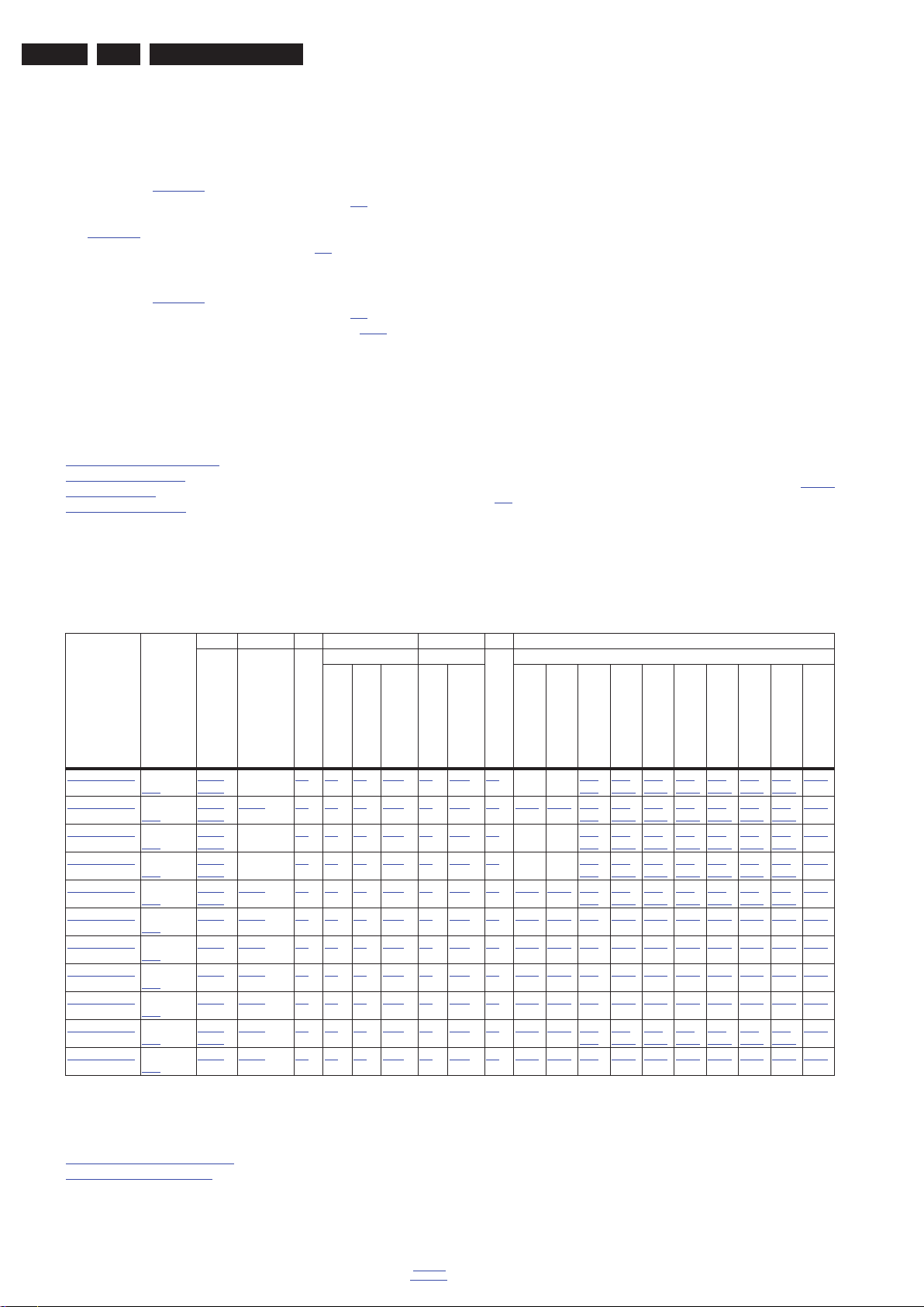
Table 2-1 Described Model Numbers and Diversity
SSB Ambilight 2 4 7 9 10
Mechanics Descriptions
CTN Styling
32PFL6606D/77 Blockbuster
32PFL7606D/78 Emmy
40PFL6606D/77 Blockbuster
40PFL6606D/78 Blockbuster
40PFL7606D/77 Emmy
40PFL7606D/78 Emmy
42PFL8606D/77 Sundance
42PFL8606D/78 Sundance
46PFL7606D/77 Emmy
46PFL7606D/78 Emmy
47PFL8606D/78 Sundance
11-1
11-1
11-2
11-2
11-2
11-2
11-3
11-3
11-2
11-2
11-3
3139 123 xxxxx
65213
- 2.3 4-1 4.3 4.3.7 7.2 7.4.1 9-1 - - 10-1
65214
65213
64833 2.3 4-2 4.3 4.3.7 7.2 7.4.1 9-1 10-21 10-23 10-1
65214
65213
- 2.3 4-3 4.3 4.3.7 7.2 7.4.1 9-2 - - 10-1
65214
65213
- 2.3 4-3 4.3 4.3.7 7.2 7.4.1 9-2 - - 10-1
65214
65213
64853 2.3 4-4 4.3 4.3.7 7.2 7.4.1 9-2 10-21 10-24 10-1
65214
65214 64853 2.3 4-4 4.3 4.3.7 7.2 7.4.1 9-2 10-21 10-24 10-9 10-10 10-11 10-12 10-13 10-14 10-15 10-18
65214 64853 2.3 4-5 4.4 4.4.8 7.2 7.4.1 9-3 10-22 10-26 10-9 10-10 10-11 10-12 10-13 10-14 10-15 10-20
65214 64853 2.3 4-5 4.4 4.4.8 7.2 7.4.1 9-3 10-22 10-26 10-9 10-10 10-11 10-12 10-13 10-14 10-15 10-20
65214 64873 2.3 4-6 4.3 4.3.7 7.2 7.4.1 9-2 10-21 10-25 10-9 10-10 10-11 10-12 10-13 10-14 10-15 10-19
65213
64873 2.3 4-6 4.3 4.3.7 7.2 7.4.1 9-2 10-21 10-25 10-1
65214
65214 64812 2.3 4-7 4.4 4.4.8 7.2 7.4.1 9-3 10-22 10-27 10-9 10-10 10-11 10-12 10-13 10-14 10-15 10-20
3104 313 xxxxx
Connection Overview
Wire Dressing
Dressing
Assembly Removal
2.1 Technical Specifications
For on-line product support please use the CTN links in Table
2-1. Here is product information available, as well as getting
started, user manuals, frequently asked questions and
software & drivers.
Schematics
LCD Removal
PSU
Wiring Diagram
Tuner
AL1 (Ambilight)
AL3 (Ambilight)
10-9
10-9
10-9
10-9
10-9
10-9
B01 (Tuner)
10-2
10-10
10-2
10-10
10-2
10-10
10-2
10-10
10-2
10-10
10-2
10-10
B02 (PNX85500)
10-3
10-11
10-3
10-11
10-3
10-11
10-3
10-11
10-3
10-11
10-3
10-11
B03 (DC/DC / Class D)
10-4
10-12
10-4
10-12
10-4
10-12
10-4
10-12
10-4
10-12
10-4
10-12
B04 (I/O)
10-5
10-13
10-5
10-13
10-5
10-13
10-5
10-13
10-5
10-13
10-5
10-13
B05 (DDR)
B06 (non-DVBS-LVDS)
10-6
10-14
10-6
10-14
10-6
10-14
10-6
10-14
10-6
10-14
10-6
10-14
B09 (non-DVBS-conn.)
10-7
10-17
10-15
10-7
10-18
10-15
10-7
10-17
10-15
10-7
10-17
10-15
10-7
10-18
10-15
10-7
10-19
10-15
E (IR/LED/Keyboard)
2.2 Directions for Use
You can download this information from the following websites:
http://www.philips.com/support
http://www.p4c.philips.com
2011-Jul-15
back to
div. table
Page 3
2.3 Connections
REAR CONNECTORS
BOTTOM REAR CONNECTORS
SIDE CONNECTORS
(3) (2)
HDMI
(1) ARC
(optional)
(optional)
(optional)
19110_051_110421.eps
110716
10
2
1
4
3
11
12
8 9
77
765
3
13
11
112345678
10000_025_090121.eps
090121
10000_017_090121.eps
090428
19
1
18 2
Technical Specifications, Diversity, and Connections
EN 3Q552.2L LA 2.
Note: The following connector colour abbreviations are used
(acc. to DIN/IEC 757): Bk= Black, Bu= Blue, Gn= Green, Gy=
Grey, Rd= Red, Wh= White, Ye= Yellow.
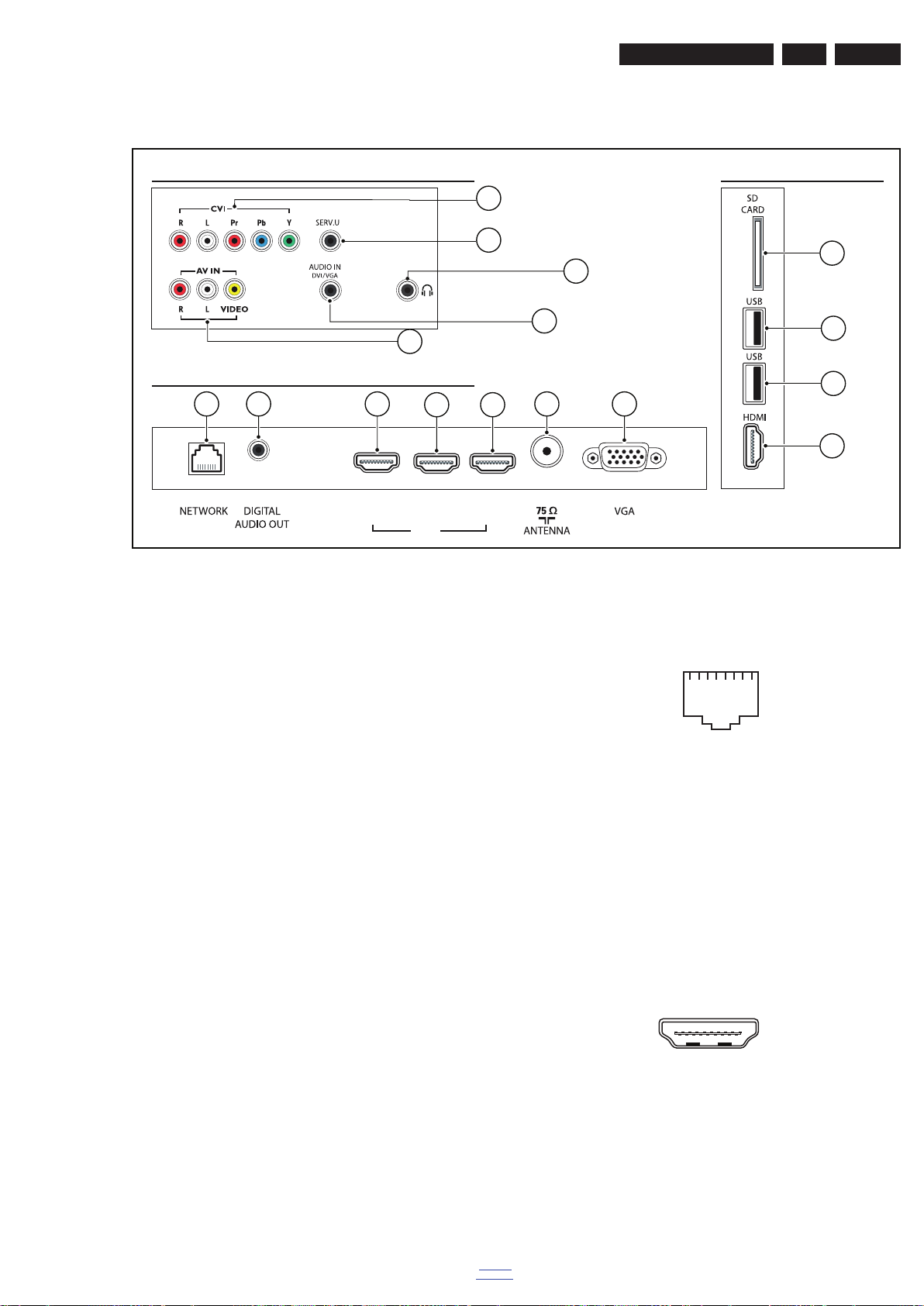
2.3.1 Rear Connections
1 - CVI: Cinch: Video YPbPr - In, Audio - In
Gn - Video Y 1 V
Bu - Video Pb 0.7 V
Rd - Video Pr 0.7 V
Rd - Audio - R 0.5 V
Wh - Audio - L 0.5 V
2 - Service Connector (UART)
1 - Ground Gnd H
2 - UART_TX Transmit k
3 - UART_RX Receive j
3 - Cinch: Audio - In (VGA/DVI)
Rd - Audio R 0.5 V
Wh - Audio L 0.5 V
4 - AV IN: Cinch: Video CVBS - In, Audio - In
Rd - Audio R 0.5 V
Wh - Audio L 0.5 V
Ye - Video CVBS 1 V
13 - Head phone (Output) (optional)
Bk - Head phone 32 - 600 ohm / 10 mW ot
Figure 2-1 Connection overview
/ 75 ohm jq
PP
/ 75 ohm jq
PP
/ 75 ohm jq
PP
/ 10 kohm jq
RMS
/ 10 kohm jq
RMS
/ 10 kohm jq
RMS
RMS
/ 10 kohm jq
/ 10 kohm jq
RMS
/ 10 kohm jq
RMS
/ 75 ohm jq
PP
back to
div. table
2.3.2 Rear Connections - Bottom
5 - RJ45: Ethernet
Figure 2-2 Ethernet connector
1 - TD+ Transmit signal k
2 - TD- Transmit signal k
3 - RD+ Receive signal j
4 - CT Centre Tap: DC level fixation
5 - CT Centre Tap: DC level fixation
6 - RD- Receive signal j
7 - GND Gnd H
8 - GND Gnd H
6 - Cinch: S/PDIF - Out
Bk - Coaxial 0.4 - 0.6V
/ 75 ohm kq
PP
7 - HDMI 2: Digital Video, Digital Audio - In
Figure 2-3 HDMI (type A) connector
1 - D2+ Data channel j
2 - Shield Gnd H
3 - D2- Data channel j
4 - D1+ Data channel j
5 - Shield Gnd H
6 - D1- Data channel j
7 - D0+ Data channel j
8 - Shield Gnd H
2011-Jul-15
Page 4
EN 4 Q552.2L LA2.
10000_017_090121.eps
090428
19
1
18 2
1
6
10
11
5
15
10000_002_090121.eps
090127
10000_049_100210.eps
100210
10
11
12
CD
GND
WP
14
GND
13
GND
1
2
3
4
5
6
7
8
9
DAT3/CS
CMD/DI
GND1
VDD
CLOCK
GND2
DAT0/D0
DAT1/IRQ
DAT2/NC
1 2 3 4
10000_022_090121.eps
090121
Technical Specifications, Diversity, and Connections
9 - D0- Data channel j
10 - CLK+ Data channel j
11 - Shield Gnd H
12 - CLK- Data channel j
13 - Easylink/CEC Control channel jk
14 - n.c.
15 - DDC_SCL DDC clock j
16 - DDC_SDA DDC data jk
17 - Ground Gnd H
18 - +5V j
19 - HPD Hot Plug Detect j
20 - Ground Gnd H
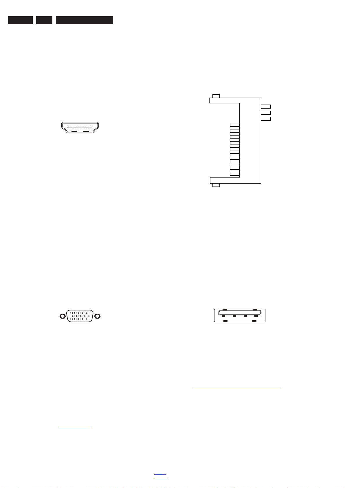
7 - HDMI 1: Digital Video - In, Digital Audio with ARC - In/
Out
Figure 2-4 HDMI (type A) connector
1 - D2+ Data channel j
2 - Shield Gnd H
3 - D2- Data channel j
4 - D1+ Data channel j
5 - Shield Gnd H
6 - D1- Data channel j
7 - D0+ Data channel j
8 - Shield Gnd H
9 - D0- Data channel j
10 - CLK+ Data channel j
11 - Shield Gnd H
12 - CLK- Data channel j
13 - Easylink/CEC Control channel jk
14 - ARC Audio Return Channel k
15 - DDC_SCL DDC clock j
16 - DDC_SDA DDC data jk
17 - Ground Gnd H
18 - +5V j
19 - HPD Hot Plug Detect j
20 - Ground Gnd H
8 - Aerial - In
- - F-type Coax, 75 ohm D
10 - Ground Sync Gnd H
11 - n.c.
12 - DDC_SDA DDC data j
13 - H-sync 0 - 5 V j
14 - V-sync 0 - 5 V j
15 - DDC_SCL DDC clock j
2.3.3 Side Connections
10 - SD-Card: Secure Digital Card - In/Out (optional)
Figure 2-6 SD-Card connector
1 - DAT3/CS Signal jk
2 - CMD/DI Signal k
3 - GND1 Gnd H
4 - Vdd Supply k
5 - CLOCK Signal k
6 - GND2 Gnd H
7 - DAT0/D0 Signal jk
8 - DAT1/IRQ Signal jk
9 - DAT2/NC Signal jk
10 - CD Signal j
11 - GND Gnd H
12 - WP Signal j
13 - GND Gnd H
14 - GND Gnd H
9 - VGA: Video RGB - In
Figure 2-5 VGA Connector
1 - Video Red 0.7 V
2 - Video Green 0.7 V
3 - Video Blue 0.7 V
4-n.c.
5 - Ground Gnd H
6 - Ground Red Gnd H
7 - Ground Green Gnd H
8 - Ground Blue Gnd H
9-+5V
2.4 Chassis Overview
Refer to chapter Block Diagrams for PWB/CBA locations.
2011-Jul-15
+5 V j
DC
11 - USB2.0
Figure 2-7 USB (type A)
/ 75 ohm j
PP
/ 75 ohm j
PP
/ 75 ohm j
PP
1-+5V k
2 - Data (-) jk
3 - Data (+) jk
4 - Ground Gnd H
12- HDMI : Digital Video, Digital Audio - In
See 7 - HDMI 2: Digital Video, Digital Audio - In
back to
div. table
Page 5

Precautions, Notes, and Abbreviation List
3. Precautions, Notes, and Abbreviation List
EN 5Q552.2L LA 3.
Index of this chapter:
3.1 Safety Instructions
3.2 Warnings
3.3 Notes
3.4 Abbreviation List
3.1 Safety Instructions
Safety regulations require the following during a repair:
• Connect the set to the Mains/AC Power via an isolation
transformer (> 800 VA).
• Replace safety components, indicated by the symbol h,
only by components identical to the original ones. Any
other component substitution (other than original type) may
increase risk of fire or electrical shock hazard.
Safety regulations require that after a repair, the set must be
returned in its original condition. Pay in particular attention to
the following points:
• Route the wire trees correctly and fix them with the
mounted cable clamps.
• Check the insulation of the Mains/AC Power lead for
external damage.
• Check the strain relief of the Mains/AC Power cord for
proper function.
• Check the electrical DC resistance between the Mains/AC
Power plug and the secondary side (only for sets that have
a Mains/AC Power isolated power supply):
1. Unplug the Mains/AC Power cord and connect a wire
between the two pins of the Mains/AC Power plug.
2. Set the Mains/AC Power switch to the “on” position
(keep the Mains/AC Power cord unplugged!).
3. Measure the resistance value between the pins of the
Mains/AC Power plug and the metal shielding of the
tuner or the aerial connection on the set. The reading
should be between 4.5 M: and 12 M:.
4. Switch “off” the set, and remove the wire between the
two pins of the Mains/AC Power plug.
• Check the cabinet for defects, to prevent touching of any
inner parts by the customer.
• Where necessary, measure the waveforms and voltages
with (D) and without (E) aerial signal. Measure the
voltages in the power supply section both in normal
operation (G) and in stand-by (F). These values are
indicated by means of the appropriate symbols.
3.3.2 Schematic Notes
• All resistor values are in ohms, and the value multiplier is
often used to indicate the decimal point location (e.g. 2K2
indicates 2.2 k:).
• Resistor values with no multiplier may be indicated with
either an “E” or an “R” (e.g. 220E or 220R indicates 220 :).
• All capacitor values are given in micro-farads (P u10
nano-farads (n u10
• Capacitor values may also use the value multiplier as the
decimal point indication (e.g. 2p2 indicates 2.2 pF).
• An “asterisk” (*) indicates component usage varies. Refer
to the diversity tables for the correct values.
• The correct component values are listed on the Philips
Spare Parts Web Portal.
3.3.3 Spare Parts
For the latest spare part overview, consult your Philips Spare
Part web portal.
3.3.4 BGA (Ball Grid Array) ICs
Introduction
For more information on how to handle BGA devices, visit this
URL: http://www.atyourservice-magazine.com
“Magazine”, then go to “Repair downloads”. Here you will find
Information on how to deal with BGA-ICs.
BGA Temperature Profiles
For BGA-ICs, you must use the correct temperature-profile.
Where applicable and available, this profile is added to the IC
Data Sheet information section in this manual.
-9
), or pico-farads (p u10
. Select
-12
-6
),
).
3.2 Warnings
• All ICs and many other semiconductors are susceptible to
electrostatic discharges (ESD w). Careless handling
during repair can reduce life drastically. Make sure that,
during repair, you are connected with the same potential as
the mass of the set by a wristband with resistance. Keep
components and tools also at this same potential.
• Be careful during measurements in the high voltage
section.
• Never replace modules or other components while the unit
is switched “on”.
• When you align the set, use plastic rather than metal tools.
This will prevent any short circuits and the danger of a
circuit becoming unstable.
3.3 Notes
3.3.1 General
• Measure the voltages and waveforms with regard to the
chassis (= tuner) ground (H), or hot ground (I), depending
on the tested area of circuitry. The voltages and waveforms
shown in the diagrams are indicative. Measure them in the
Service Default Mode with a colour bar signal and stereo
sound (L: 3 kHz, R: 1 kHz unless stated otherwise) and
picture carrier at 475.25 MHz for PAL, or 61.25 MHz for
NTSC (channel 3).
3.3.5 Lead-free Soldering
Due to lead-free technology some rules have to be respected
by the workshop during a repair:
• Use only lead-free soldering tin. If lead-free solder paste is
required, please contact the manufacturer of your soldering
equipment. In general, use of solder paste within
workshops should be avoided because paste is not easy to
store and to handle.
• Use only adequate solder tools applicable for lead-free
soldering tin. The solder tool must be able:
– To reach a solder-tip temperature of at least 400°C.
– To stabilize the adjusted temperature at the solder-tip.
– To exchange solder-tips for different applications.
• Adjust your solder tool so that a temperature of around
360°C - 380°C is reached and stabilized at the solder joint.
Heating time of the solder-joint should not exceed ~ 4 sec.
Avoid temperatures above 400°C, otherwise wear-out of
tips will increase drastically and flux-fluid will be destroyed.
To avoid wear-out of tips, switch “off” unused equipment or
reduce heat.
• Mix of lead-free soldering tin/parts with leaded soldering
tin/parts is possible but PHILIPS recommends strongly to
avoid mixed regimes. If this cannot be avoided, carefully
clear the solder-joint from old tin and re-solder with new tin.
3.3.6 Alternative BOM identification
It should be noted that on the European Service website,
“Alternative BOM” is referred to as “Design variant”.
back to
div. table
2011-Jul-15
Page 6
EN 6 Q552.2L LA3.
10000_053_110228.eps
110228
Precautions, Notes, and Abbreviation List
The third digit in the serial number (example:
AG2B0335000001) indicates the number of the alternative
B.O.M. (Bill Of Materials) that has been used for producing the
specific TV set. In general, it is possible that the same TV
model on the market is produced with e.g. two different types
of displays, coming from two different suppliers. This will then
result in sets which have the same CTN (Commercial Type
Number; e.g. 28PW9515/12) but which have a different B.O.M.
number.
By looking at the third digit of the serial number, one can
identify which B.O.M. is used for the TV set he is working with.
If the third digit of the serial number contains the number “1”
(example: AG1B033500001), then the TV set has been
manufactured according to B.O.M. number 1. If the third digit is
a “2” (example: AG2B0335000001), then the set has been
produced according to B.O.M. no. 2. This is important for
ordering the correct spare parts!
For the third digit, the numbers 1...9 and the characters A...Z
can be used, so in total: 9 plus 26= 35 different B.O.M.s can be
indicated by the third digit of the serial number.
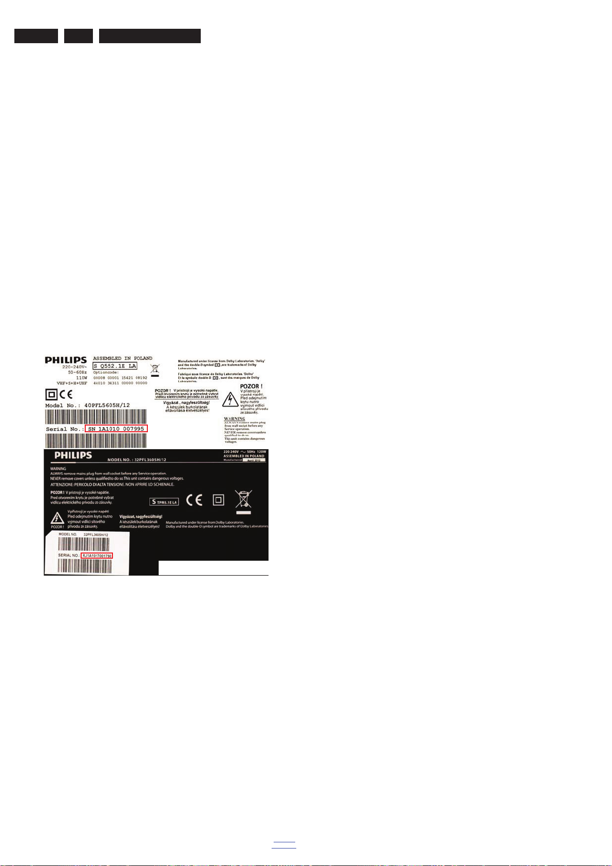
Identification: The bottom line of a type plate gives a 14-digit
serial number. Digits 1 and 2 refer to the production centre (e.g.
SN is Lysomice, RJ is Kobierzyce), digit 3 refers to the B.O.M.
code, digit 4 refers to the Service version change code, digits 5
and 6 refer to the production year, and digits 7 and 8 refer to
production week (in example below it is 2010 week 10 / 2010
week 17). The 6 last digits contain the serial number.
Figure 3-1 Serial number (example)
3.3.7 Board Level Repair (BLR) or Component Level Repair
(CLR)
If a board is defective, consult your repair procedure to decide
if the board has to be exchanged or if it should be repaired on
component level.
If your repair procedure says the board should be exchanged
completely, do not solder on the defective board. Otherwise, it
cannot be returned to the O.E.M. supplier for back charging!
3.3.8 Practical Service Precautions
• It makes sense to avoid exposure to electrical shock.
While some sources are expected to have a possible
dangerous impact, others of quite high potential are of
limited current and are sometimes held in less regard.
• Always respect voltages. While some may not be
dangerous in themselves, they can cause unexpected
reactions that are best avoided. Before reaching into a
powered TV set, it is best to test the high voltage insulation.
It is easy to do, and is a good service precaution.
3.4 Abbreviation List
0/6/12 SCART switch control signal on A/V
board. 0 = loop through (AUX to TV),
6 = play 16 : 9 format, 12 = play 4 : 3
format
AARA Automatic Aspect Ratio Adaptation:
algorithm that adapts aspect ratio to
remove horizontal black bars; keeps
the original aspect ratio
ACI Automatic Channel Installation:
algorithm that installs TV channels
directly from a cable network by
means of a predefined TXT page
ADC Analogue to Digital Converter
AFC Automatic Frequency Control: control
signal used to tune to the correct
frequency
AGC Automatic Gain Control: algorithm that
controls the video input of the feature
box
AM Amplitude Modulation
AP Asia Pacific
AR Aspect Ratio: 4 by 3 or 16 by 9
ASF Auto Screen Fit: algorithm that adapts
aspect ratio to remove horizontal black
bars without discarding video
information
ATSC Advanced Television Systems
Committee, the digital TV standard in
the USA
ATV See Auto TV
Auto TV A hardware and software control
system that measures picture content,
and adapts image parameters in a
dynamic way
AV External Audio Video
AVC Audio Video Controller
AVIP Audio Video Input Processor
B/G Monochrome TV system. Sound
carrier distance is 5.5 MHz
BDS Business Display Solutions (iTV)
BLR Board-Level Repair
BTSC Broadcast Television Standard
Committee. Multiplex FM stereo sound
system, originating from the USA and
used e.g. in LATAM and AP-NTSC
countries
B-TXT Blue TeleteXT
C Centre channel (audio)
CEC Consumer Electronics Control bus:
remote control bus on HDMI
connections
CL Constant Level: audio output to
connect with an external amplifier
CLR Component Level Repair
ComPair Computer aided rePair
CP Connected Planet / Copy Protection
CSM Customer Service Mode
CTI Color Transient Improvement:
manipulates steepness of chroma
transients
CVBS Composite Video Blanking and
Synchronization
DAC Digital to Analogue Converter
DBE Dynamic Bass Enhancement: extra
low frequency amplification
DCM Data Communication Module. Also
referred to as System Card or
Smartcard (for iTV).
DDC See “E-DDC”
D/K Monochrome TV system. Sound
carrier distance is 6.5 MHz
DFI Dynamic Frame Insertion
2011-Jul-15
back to
div. table
Page 7

Precautions, Notes, and Abbreviation List
EN 7Q552.2L LA 3.
DFU Directions For Use: owner's manual
DMR Digital Media Reader: card reader
DMSD Digital Multi Standard Decoding
DNM Digital Natural Motion
DNR Digital Noise Reduction: noise
reduction feature of the set
DRAM Dynamic RAM
DRM Digital Rights Management
DSP Digital Signal Processing
DST Dealer Service Tool: special remote
control designed for service
technicians
DTCP Digital Transmission Content
Protection; A protocol for protecting
digital audio/video content that is
traversing a high speed serial bus,
such as IEEE-1394
DVB-C Digital Video Broadcast - Cable
DVB-T Digital Video Broadcast - Terrestrial
DVD Digital Versatile Disc
DVI(-d) Digital Visual Interface (d= digital only)
E-DDC Enhanced Display Data Channel
(VESA standard for communication
channel and display). Using E-DDC,
the video source can read the EDID
information form the display.
EDID Extended Display Identification Data
(VESA standard)
EEPROM Electrically Erasable and
Programmable Read Only Memory
EMI Electro Magnetic Interference
EPG Electronic Program Guide
EPLD Erasable Programmable Logic Device
EU Europe
EXT EXTernal (source), entering the set by
SCART or by cinches (jacks)
FDS Full Dual Screen (same as FDW)
FDW Full Dual Window (same as FDS)
FLASH FLASH memory
FM Field Memory or Frequency
Modulation
FPGA Field-Programmable Gate Array
FTV Flat TeleVision
Gb/s Giga bits per second
G-TXT Green TeleteXT
H H_sync to the module
HD High Definition
HDD Hard Disk Drive
HDCP High-bandwidth Digital Content
Protection: A “key” encoded into the
HDMI/DVI signal that prevents video
data piracy. If a source is HDCP coded
and connected via HDMI/DVI without
the proper HDCP decoding, the
picture is put into a “snow vision” mode
or changed to a low resolution. For
normal content distribution the source
and the display device must be
enabled for HDCP “software key”
decoding.
HDMI High Definition Multimedia Interface
HP HeadPhone
I Monochrome TV system. Sound
2
I
C Inter IC bus
2
I
D Inter IC Data bus
2
I
S Inter IC Sound bus
carrier distance is 6.0 MHz
IF Intermediate Frequency
IR Infra Red
IRQ Interrupt Request
ITU-656 The ITU Radio communication Sector
(ITU-R) is a standards body
subcommittee of the International
Telecommunication Union relating to
radio communication. ITU-656 (a.k.a.
back to
div. table
SDI), is a digitized video format used
for broadcast grade video.
Uncompressed digital component or
digital composite signals can be used.
The SDI signal is self-synchronizing,
uses 8 bit or 10 bit data words, and has
a maximum data rate of 270 Mbit/s,
with a minimum bandwidth of 135
MHz.
iTV Institutional TeleVision; TV sets for
hotels, hospitals etc.
LS Last Status; The settings last chosen
by the customer and read and stored
in RAM or in the NVM. They are called
at start-up of the set to configure it
according to the customer's
preferences
LATAM Latin America
LCD Liquid Crystal Display
LED Light Emitting Diode
L/L' Monochrome TV system. Sound
carrier distance is 6.5 MHz. L' is Band
I, L is all bands except for Band I
LPL LG.Philips LCD (supplier)
LS Loudspeaker
LVDS Low Voltage Differential Signalling
Mbps Mega bits per second
M/N Monochrome TV system. Sound
carrier distance is 4.5 MHz
MHEG Part of a set of international standards
related to the presentation of
multimedia information, standardised
by the Multimedia and Hypermedia
Experts Group. It is commonly used as
a language to describe interactive
television services
MIPS Microprocessor without Interlocked
Pipeline-Stages; A RISC-based
microprocessor
MOP Matrix Output Processor
MOSFET Metal Oxide Silicon Field Effect
Transistor, switching device
MPEG Motion Pictures Experts Group
MPIF Multi Platform InterFace
MUTE MUTE Line
MTV Mainstream TV: TV-mode with
Consumer TV features enabled (iTV)
NC Not Connected
NICAM Near Instantaneous Compounded
Audio Multiplexing. This is a digital
sound system, mainly used in Europe.
NTC Negative Temperature Coefficient,
non-linear resistor
NTSC National Television Standard
Committee. Color system mainly used
in North America and Japan. Color
carrier NTSC M/N= 3.579545 MHz,
NTSC 4.43= 4.433619 MHz (this is a
VCR norm, it is not transmitted off-air)
NVM Non-Volatile Memory: IC containing
TV related data such as alignments
O/C Open Circuit
OSD On Screen Display
OAD Over the Air Download. Method of
software upgrade via RF transmission.
Upgrade software is broadcasted in
TS with TV channels.
OTC On screen display Teletext and
Control; also called Artistic (SAA5800)
P50 Project 50: communication protocol
between TV and peripherals
PAL Phase Alternating Line. Color system
mainly used in West Europe (colour
carrier = 4.433619 MHz) and South
America (colour carrier
2011-Jul-15
Page 8

EN 8 Q552.2L LA3.
Precautions, Notes, and Abbreviation List
PAL M = 3.575612 MHz and
PAL N = 3.582056 MHz)
PCB Printed Circuit Board (same as “PWB”)
PCM Pulse Code Modulation
PDP Plasma Display Panel
PFC Power Factor Corrector (or Pre-
conditioner)
PIP Picture In Picture
PLL Phase Locked Loop. Used for e.g.
FST tuning systems. The customer
can give directly the desired frequency
POD Point Of Deployment: a removable
CAM module, implementing the CA
system for a host (e.g. a TV-set)
POR Power On Reset, signal to reset the uP
PSDL Power Supply for Direct view LED
backlight with 2D-dimming
PSL Power Supply with integrated LED
drivers
PSLS Power Supply with integrated LED
drivers with added Scanning
functionality
PTC Positive Temperature Coefficient,
non-linear resistor
PWB Printed Wiring Board (same as “PCB”)
PWM Pulse Width Modulation
QRC Quasi Resonant Converter
QTNR Quality Temporal Noise Reduction
QVCP Quality Video Composition Processor
RAM Random Access Memory
RGB Red, Green, and Blue. The primary
color signals for TV. By mixing levels
of R, G, and B, all colors (Y/C) are
reproduced.
RC Remote Control
RC5 / RC6 Signal protocol from the remote
control receiver
RESET RESET signal
ROM Read Only Memory
RSDS Reduced Swing Differential Signalling
data interface
R-TXT Red TeleteXT
SAM Service Alignment Mode
S/C Short Circuit
SCART Syndicat des Constructeurs
d'Appareils Radiorécepteurs et
Téléviseurs
SCL Serial Clock I
2
C
SCL-F CLock Signal on Fast I
SD Standard Definition
SDA Serial Data I
2
C
SDA-F DAta Signal on Fast I
SDI Serial Digital Interface, see “ITU-656”
SDRAM Synchronous DRAM
SECAM SEequence Couleur Avec Mémoire.
Colour system mainly used in France
and East Europe. Colour
carriers = 4.406250 MHz and
4.250000 MHz
SIF Sound Intermediate Frequency
SMPS Switched Mode Power Supply
SoC System on Chip
SOG Sync On Green
SOPS Self Oscillating Power Supply
SPI Serial Peripheral Interface bus; a 4-
wire synchronous serial data link
standard
S/PDIF Sony Philips Digital InterFace
SRAM Static RAM
SRP Service Reference Protocol
SSB Small Signal Board
SSC Spread Spectrum Clocking, used to
reduce the effects of EMI
STB Set Top Box
STBY STand-BY
2011-Jul-15
2
C bus
2
C bus
back to
div. table
SVGA 800 × 600 (4:3)
SVHS Super Video Home System
SW Software
SWAN Spatial temporal Weighted Averaging
Noise reduction
SXGA 1280 × 1024
TFT Thin Film Transistor
THD Total Harmonic Distortion
TMDS Transmission Minimized Differential
Signalling
TS Transport Stream
TXT TeleteXT
TXT-DW Dual Window with TeleteXT
UI User Interface
uP Microprocessor
UXGA 1600 × 1200 (4:3)
V V-sync to the module
VESA Video Electronics Standards
Association
VGA 640 × 480 (4:3)
VL Variable Level out: processed audio
output toward external amplifier
VSB Vestigial Side Band; modulation
method
WYSIWYR What You See Is What You Record:
record selection that follows main
picture and sound
WXGA 1280 × 768 (15:9)
XTAL Quartz crystal
XGA 1024 × 768 (4:3)
Y Luminance signal
Y/C Luminance (Y) and Chrominance (C)
signal
YPbPr Component video. Luminance and
scaled color difference signals (B-Y
and R-Y)
YUV Component video
Page 9
4. Mechanical Instructions
19111_012_110519.eps
110519
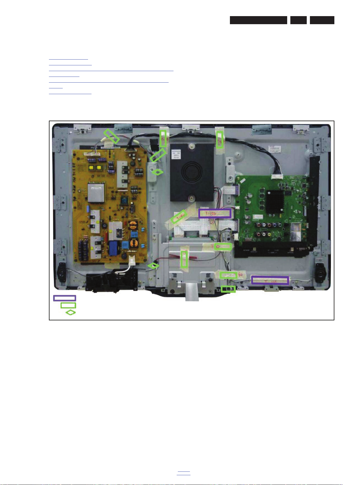
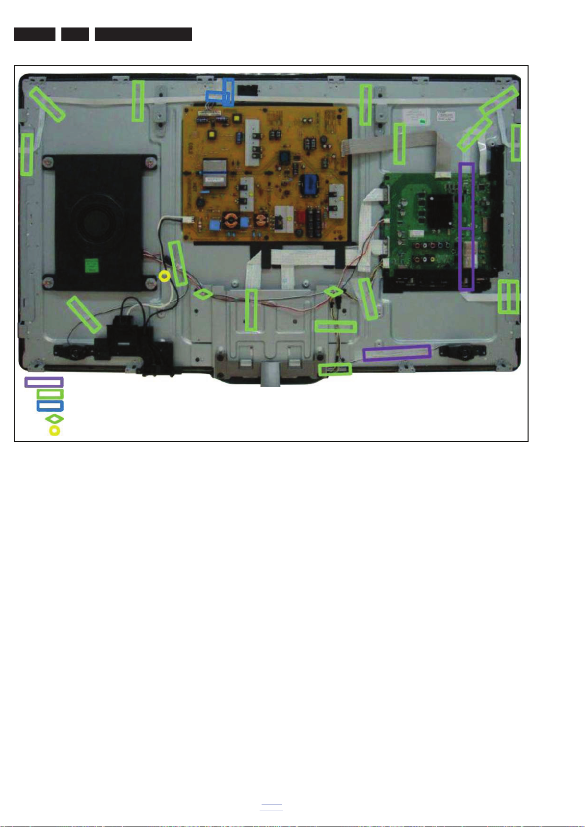
Tape (150 m.m.) 2 ×
Tape (80 m.m.) 9 ×
Clamp (11 m.m.) 2 ×
Mechanical Instructions
EN 9Q552.2L LA 4.
Index of this chapter:
4.1 Cable Dressing
4.2 Service Positions
4.3 Assy/Panel Removal Blockbuster/Emmy Styling (xxPFL6/
7xxx/xx series)
4.4 Assy/Panel Removal Sundance Styling (xxPFL8xxx/xx
series)
4.5 Set Re-assembly
4.1 Cable Dressing
Notes:
• Figures below can deviate slightly from the actual situation,
due to the different set executions.
Figure 4-1 Cable dressing 32PFL6606D/7x (Blockbuster)
back to
div. table
2011-Jul-15
Page 10
EN 10 Q552.2L LA4.
19111_016_110520.eps
110520
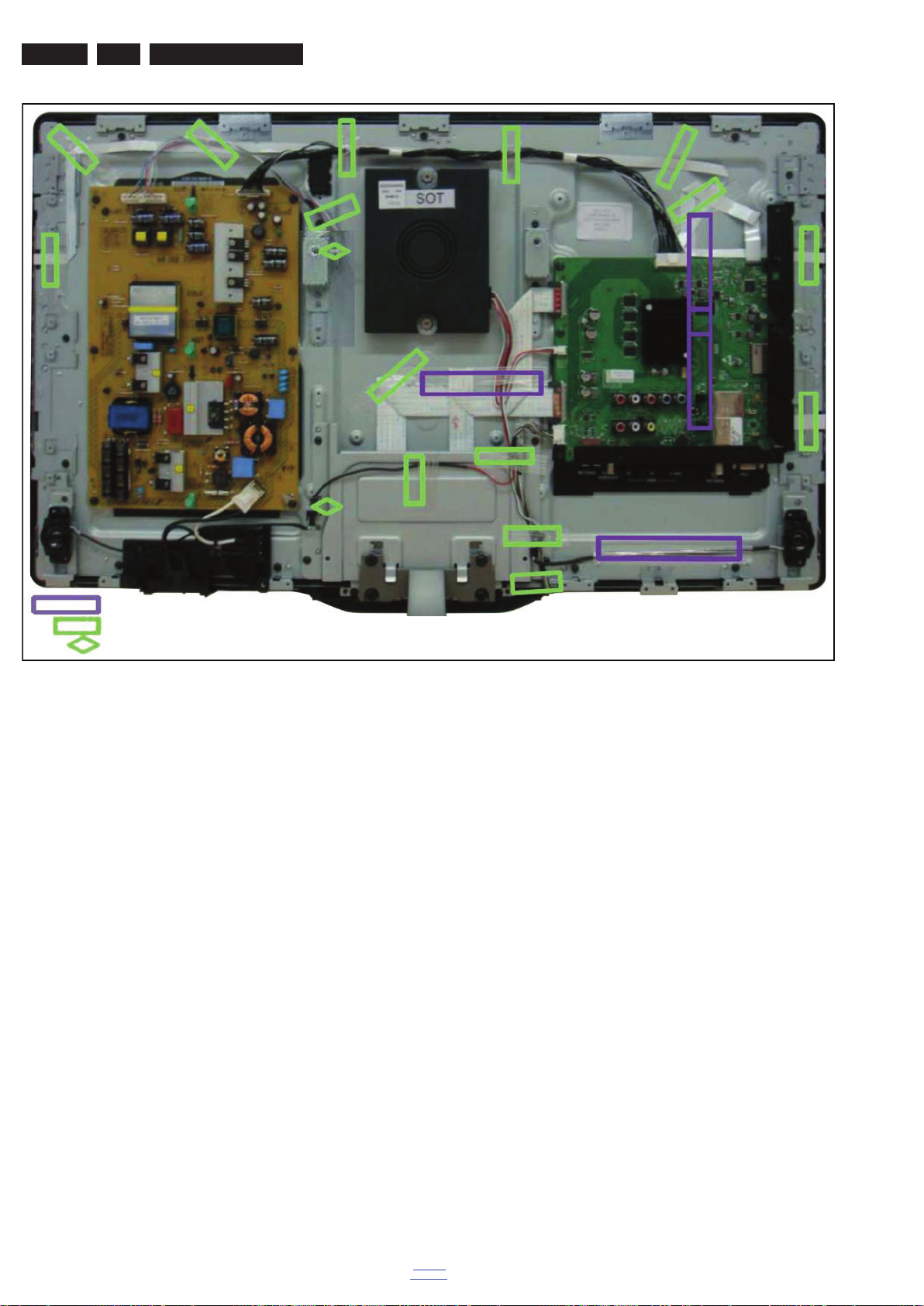
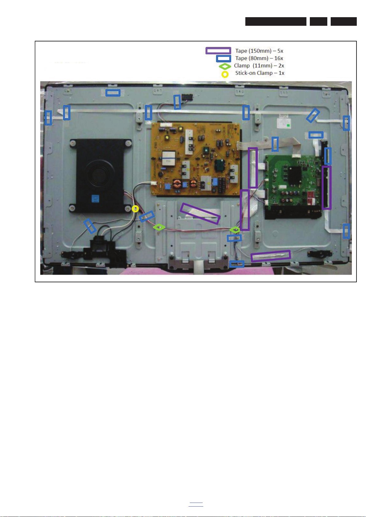
Tape (150 m.m.) 4 ×
Tape (80 m.m.) 15 ×
Clamp (11 m.m.) 2 ×
Mechanical Instructions
Figure 4-2 Cable dressing 32PFL7606D/7x (Emmy)
2011-Jul-15
back to
div. table
Page 11
Mechanical Instructions
19111_013_110519.eps
110519
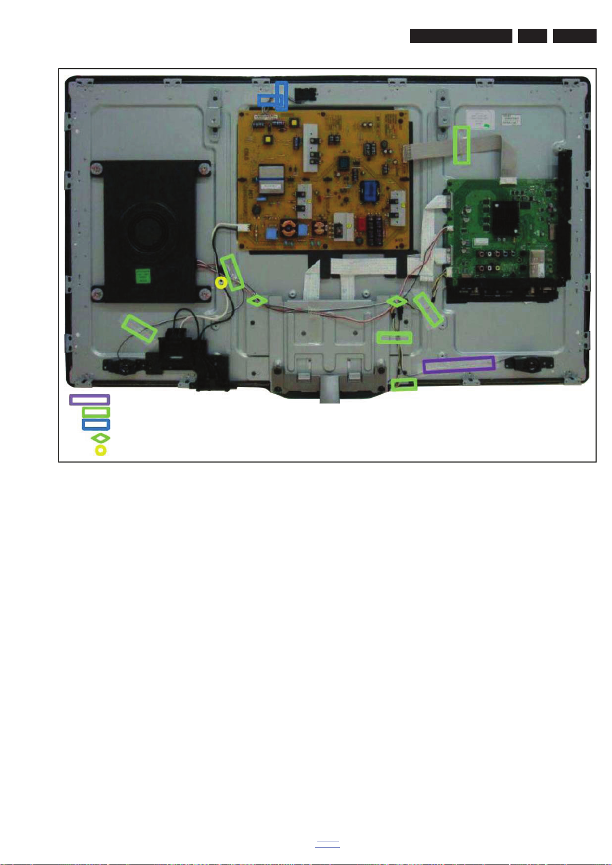
Tape (150 m.m.) 1 ×
Tape (80 m.m.) 6 ×
Tape (50 m.m.) 2 ×
Clamp (11 m.m.) 2 ×
Stick-on Clamp 1 ×
EN 11Q552.2L LA 4.
Figure 4-3 Cable dressing 40PFL6606D/7x (Blockbuster)
back to
div. table
2011-Jul-15
Page 12
EN 12 Q552.2L LA4.
19111_014_110519.eps
110519
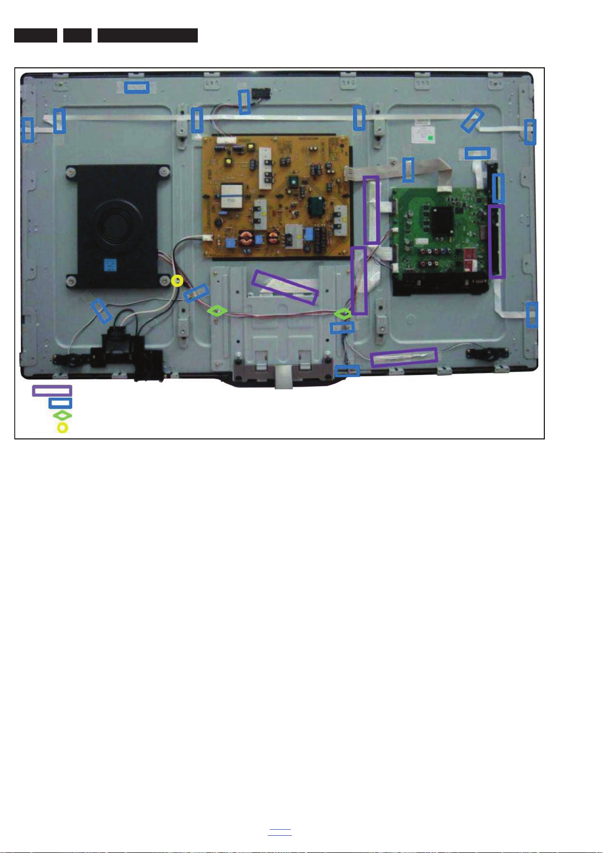
Tape (150 m.m.) 3 ×
Tape (80 m.m.) 16 ×
Tape (50 m.m.) 2 ×
Clamp (11 m.m.) 2 ×
Stick-on Clamp 1 ×
Mechanical Instructions
2011-Jul-15
Figure 4-4 Cable dressing 40PFL7606D/7x (Emmy)
back to
div. table
Page 13
Mechanical Instructions
19112_100_110712.eps
110712
EN 13Q552.2L LA 4.
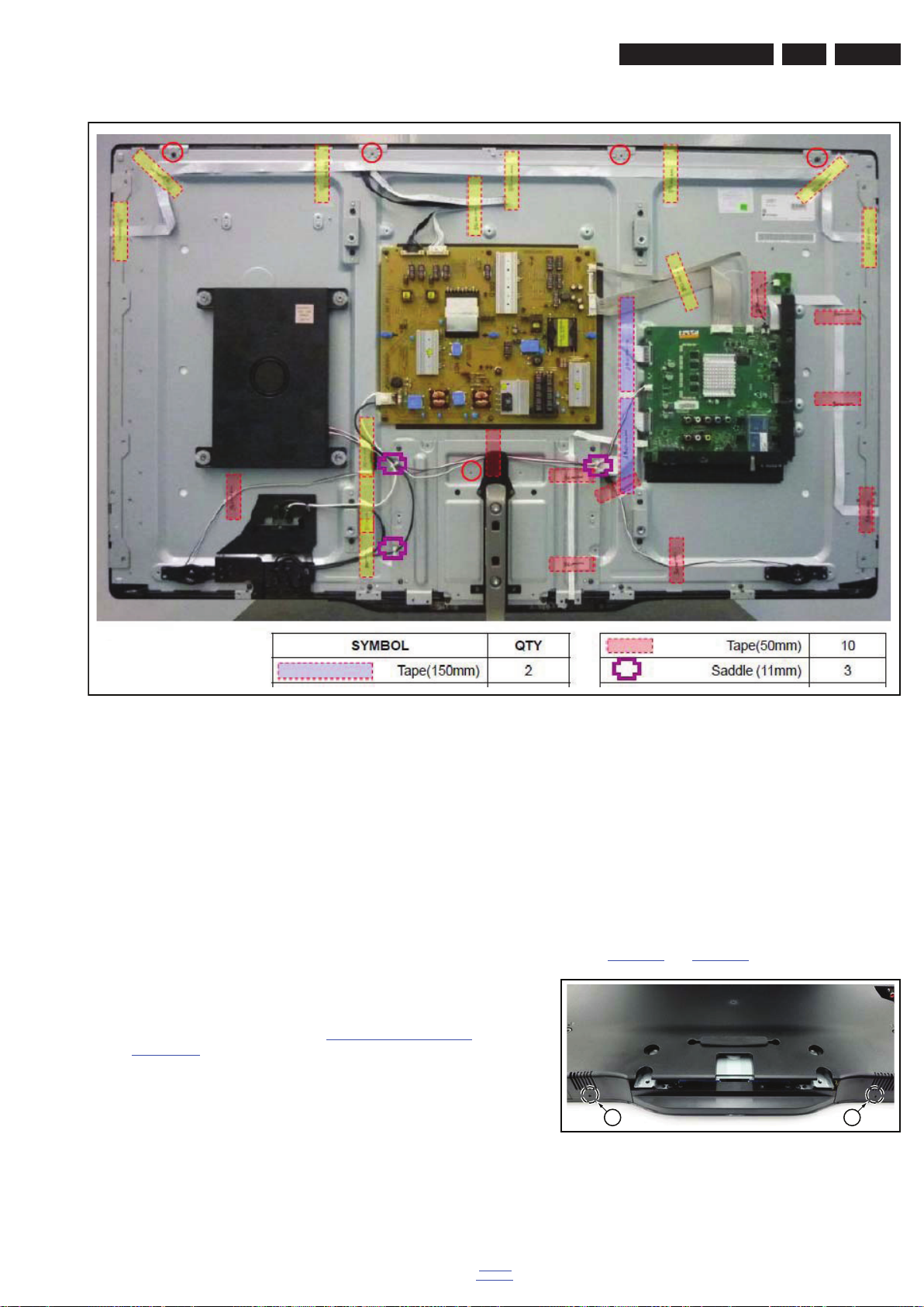
Figure 4-5 Cable dressing 42PFL8606D/7x (Sundance)
back to
div. table
2011-Jul-15
Page 14
EN 14 Q552.2L LA4.
19111_015_110519.eps
110519
Mechanical Instructions
Tape (150 m.m.) 5 ×
Tape (80 m.m.) 16 ×
Clamp (11 m.m.) 2 ×
Stick-on Clamp 1 ×
Figure 4-6 Cable dressing 46PFL7606D/7x (Emmy)
2011-Jul-15
back to
div. table
Page 15
Mechanical Instructions
19112_101_110712.eps
110712
19100_048_110216.eps
110216
1 1
EN 15Q552.2L LA 4.
Figure 4-7 Cable dressing 47PFL8606D/7x (Sundance)
4.2 Service Positions
For easy servicing of a TV set, the set should be put face down
on a soft flat surface, foam buffers or other specific workshop
tools. Ensure that a stable situation is created to perform
measurements and alignments. When using foam bars take
care that these always support the cabinet and never only the
display. Caution: Failure to follow these guidelines can
seriously damage the display!
Ensure that ESD safe measures are taken.
4.3 Assy/Panel Removal Blockbuster/Emmy
Styling (xxPFL6/7xxx/xx series)
For the 40" and 46" sets, additional instructions (rear cover
removal) apply. Refer to subsection Additional instructions 40"
and 46" sets.
The instructions apply to the 37PFL6606H/12 (Blockbuster European model) - without Ambilight. At time of publishing of
this manual, no data was available for the Ambilight models
(series xxPFL7606D/xx - Emmy).
4.3.1 Rear Cover
Warning: Disconnect the mains power cord before you remove
the rear cover.
Note: it is not necessary to remove the stand while removing
the rear cover.
1. Remove all screws of the rear cover.
2. Lift the rear cover from the TV. Make sure that wires and
flat coils are not damaged while lifting the rear cover from
the set.
Additional instructions 40" and 46" sets
40"and 46" sets have a dedicated method to open the bottom
catches when removing the rear cover.
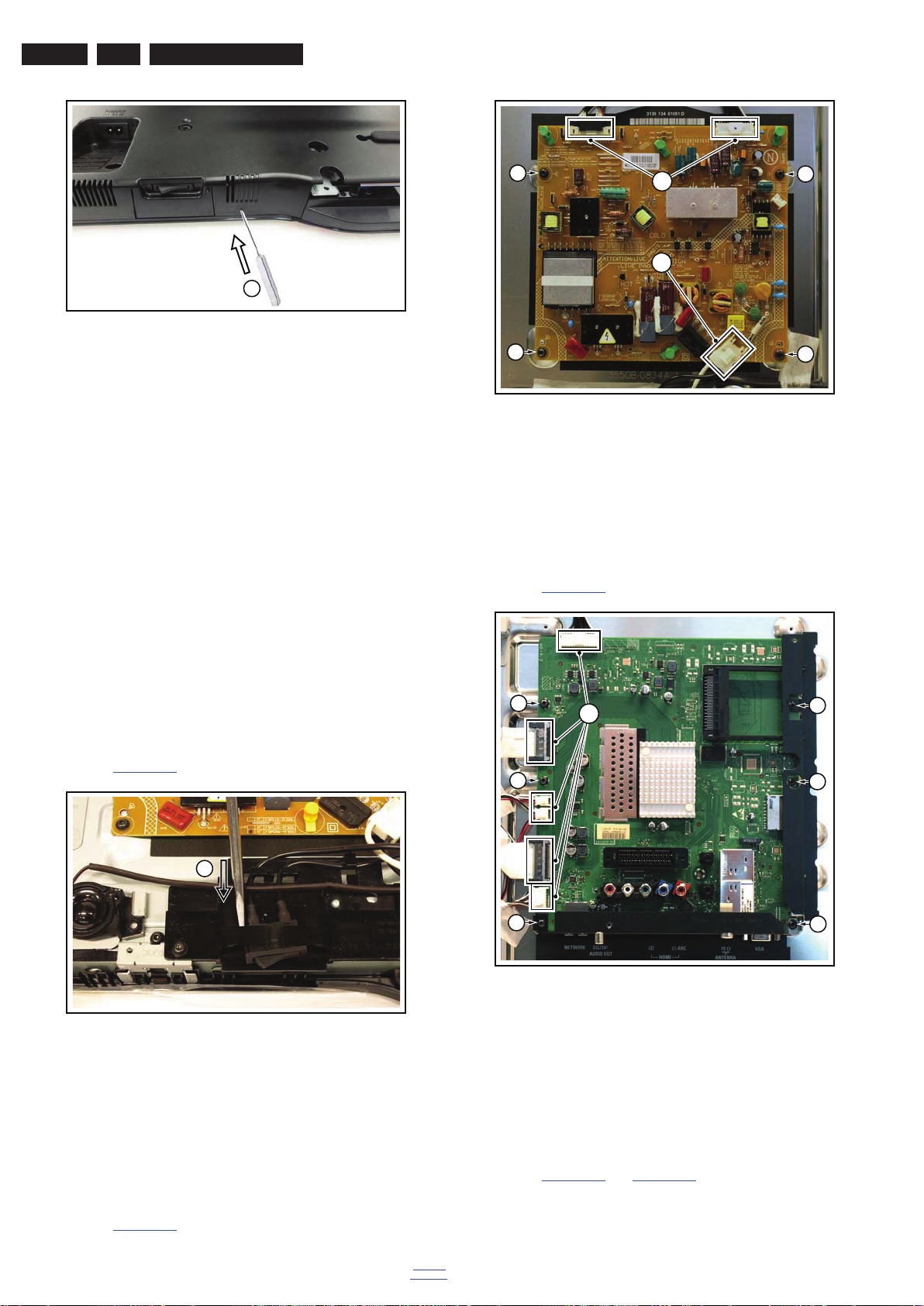
Refer to Figure 4-8
and Figure 4-9 for details.
Figure 4-8 Bottom catches 40" and 46" sets -1-
back to
div. table
2011-Jul-15
Page 16
EN 16 Q552.2L LA4.
19100_049_110216.eps
110216
2
19100_047_110216.eps
110216
1
19101_008_110407.eps
110407
2
2
2
2
1
1
19101_007_110407.eps
110407
2
2
2
2
2
2
1
Figure 4-9 Bottom catches 40" and 46" sets -2-
It is advised to lay the set with front facing down before
executing this operation.
1. Remove all screws from the rear cover.
2. Use a round rod (diameter 2 mm) and insert it in one of the
holes [1].
3. Push the catch located inside the rear cover away by
inserting the rod [2] through the hole and lifting the rear
cover at the same time.
4. Repeat the same procedure on the other hole.
Mechanical Instructions
Figure 4-11 Main Power Supply
1. Unplug all connectors [1].
2. Remove the fixation screws [2].
3. Take the board out.
When defective, replace the whole unit.
4.3.2 Speakers
Tweeters
Each tweeter unit is mounted with two screws.
When defective, replace the whole unit.
Subwoofer
The central subwoofer is located in the centre of the set and is
secured by two bosses.
When defective, replace the whole unit.
4.3.3 Mains Switch
Refer to Figure 4-10
for details.
4.3.5 Small Signal Board (SSB)
Refer to Figure 4-12
for details.
4.3.4 Main Power Supply
2011-Jul-15
Figure 4-10 Mains switch
The mains switch is mounted on a plastic subframe and can be
removed without removing the subframe.
1. Use a screwdriver and push the switch out of its casing [1].
2. Unplug the connectors.
When defective, replace the whole unit.
Refer to Figure 4-11
for details.
Figure 4-12 SSB
1. Unplug all connectors [1].
2. Remove the fixation screws [2].
3. Take the board out.
When remounting, ensure that the side shielding is positioned
correctly.
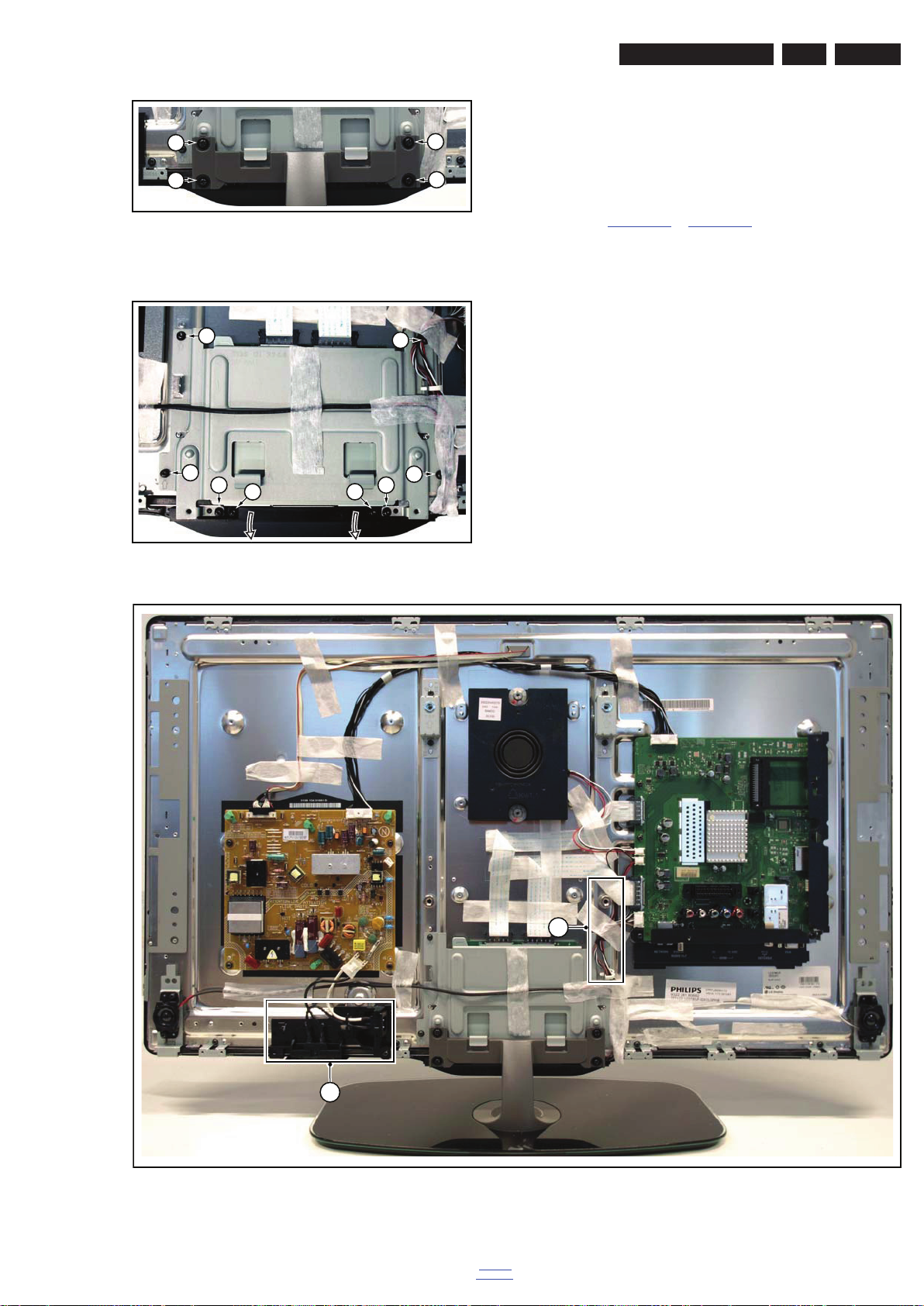
4.3.6 Keyboard Control, IR & LED Board
back to
div. table
Refer to Figure 4-13
and Figure 4-14 for details.
Page 17
Mechanical Instructions
19101_009_110407.eps
110407
1
1
1
1
19101_006_110407.eps
110407
2
2
2 2
2
2
3 3
19101_005_110407.eps
110407
2
1
1. Remove the stand [1].
2. Remove the stand subframe [2].
3. Remove the screws [3], unplug the connector and take the
board out.
When defective, replace the whole unit.
4.3.7 LCD Panel
EN 17Q552.2L LA 4.
Figure 4-13 Keyboard control, IR & LED board [1/2]
Figure 4-14 Keyboard control, IR & LED board [2/2]
Refer to Figure 4-15
1. Remove the SSB as described earlier.
2. Remove the PSU as described earlier.
3. Remove the tweeters with their subframes and subwoofer
as described earlier.
4. Remove the stand and -subframe as described earlier.
5. Remove the cables [1].
6. Remove the mains switch subframe [2].
7. Remove the keyboard control-, and IR & LED board as
described earlier.
8. Remove all remaining cables and subframes.
9. Use a screwdriver to release the catches [3] that secure the
panel.
10. Use a screwdriver to release the catches and remove the
sidewings [4] that secure the panel.
11. Take the panel out.
Remove the clamps from the panel before sending the panel in
for Service.
to Figure 4-17 for details.
Figure 4-15 LCD panel [1/3]
back to
div. table
2011-Jul-15
Page 18
EN 18 Q552.2L LA4.
19101_004_110407.eps
110407
3
19101_003_110407.eps
110407
4
19100_047_110216.eps
110216
1
19100_050_110216.eps
110216
1
1
1
22
2
2
Mechanical Instructions
When defective, replace the whole unit.
Subwoofer
The central subwoofer is located in the centre of the set and is
secured by two bosses.
When defective, replace the whole unit.
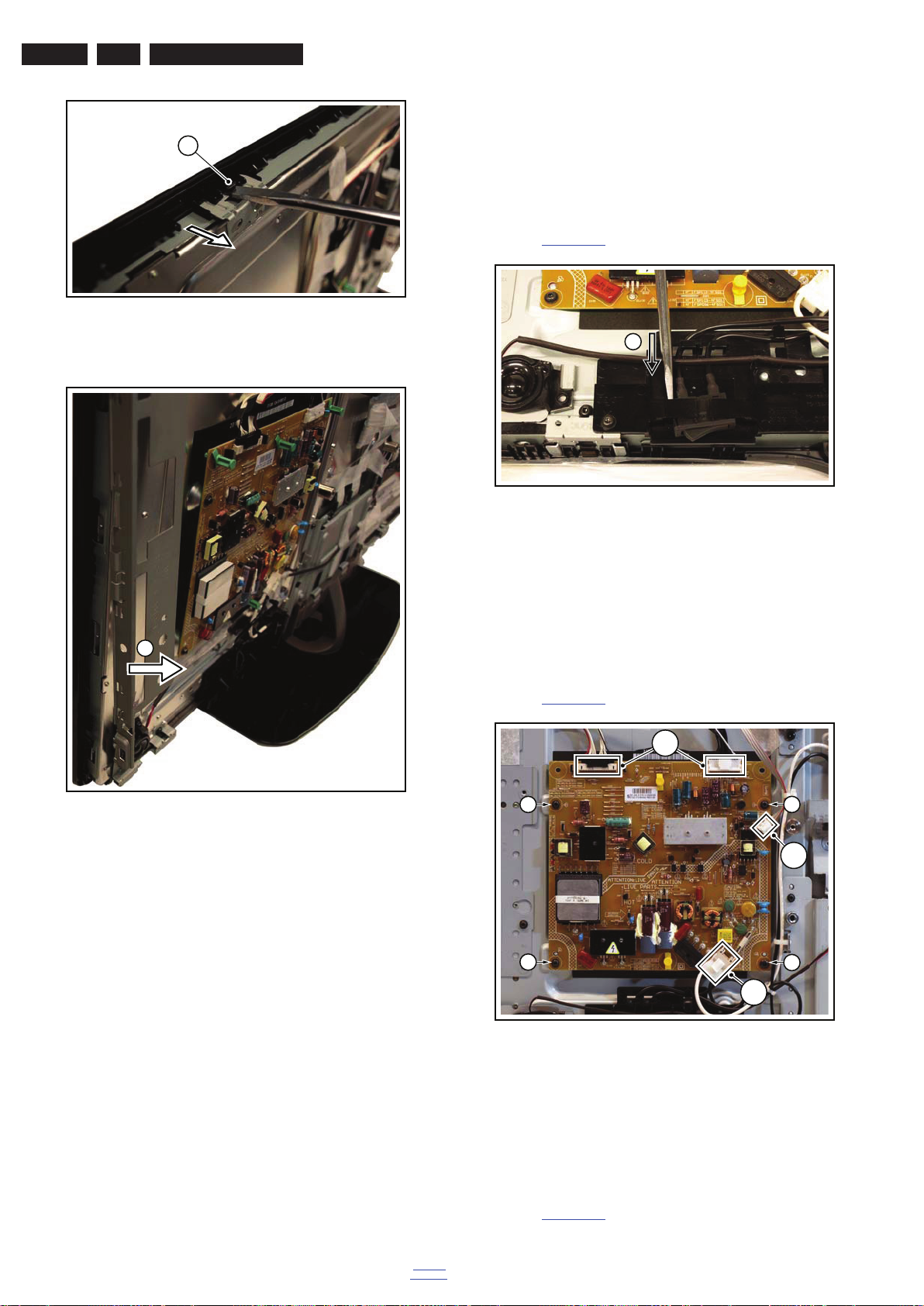
4.4.3 Mains Switch
Figure 4-16 LCD panel [2/3]
Refer to Figure 4-18
for details.
Figure 4-18 Mains switch
The mains switch is mounted on a plastic subframe and can be
removed without removing the subframe.
1. Use a screwdriver and push the switch out of its casing [1].
2. Unplug the connectors.
When defective, replace the whole unit.
4.4.4 Main Power Supply
Figure 4-17 LCD panel [3/3]
4.4 Assy/Panel Removal Sundance Styling
(xxPFL8xxx/xx series)
The instructions apply to the 32PFL7406K/02 - European
model.
4.4.1 Rear Cover
Warning: Disconnect the mains power cord before you remove
the rear cover.
Note: it is not necessary to remove the stand while removing
the rear cover.
1. Remove all screws of the rear cover.
2. Lift the rear cover from the TV. Make sure that wires and
flat coils are not damaged while lifting the rear cover from
the set.
Refer to Figure 4-19
for details.
Figure 4-19 Main Power Supply
1. Unplug all connectors [1].
2. Remove the fixation screws [2].
3. Take the board out.
When defective, replace the whole unit.
4.4.2 Speakers
Tweeters
Each tweeter unit is mounted with one screw.
2011-Jul-15
4.4.5 Small Signal Board (SSB)
Refer to Figure 4-20
back to
div. table
for details.
Page 19
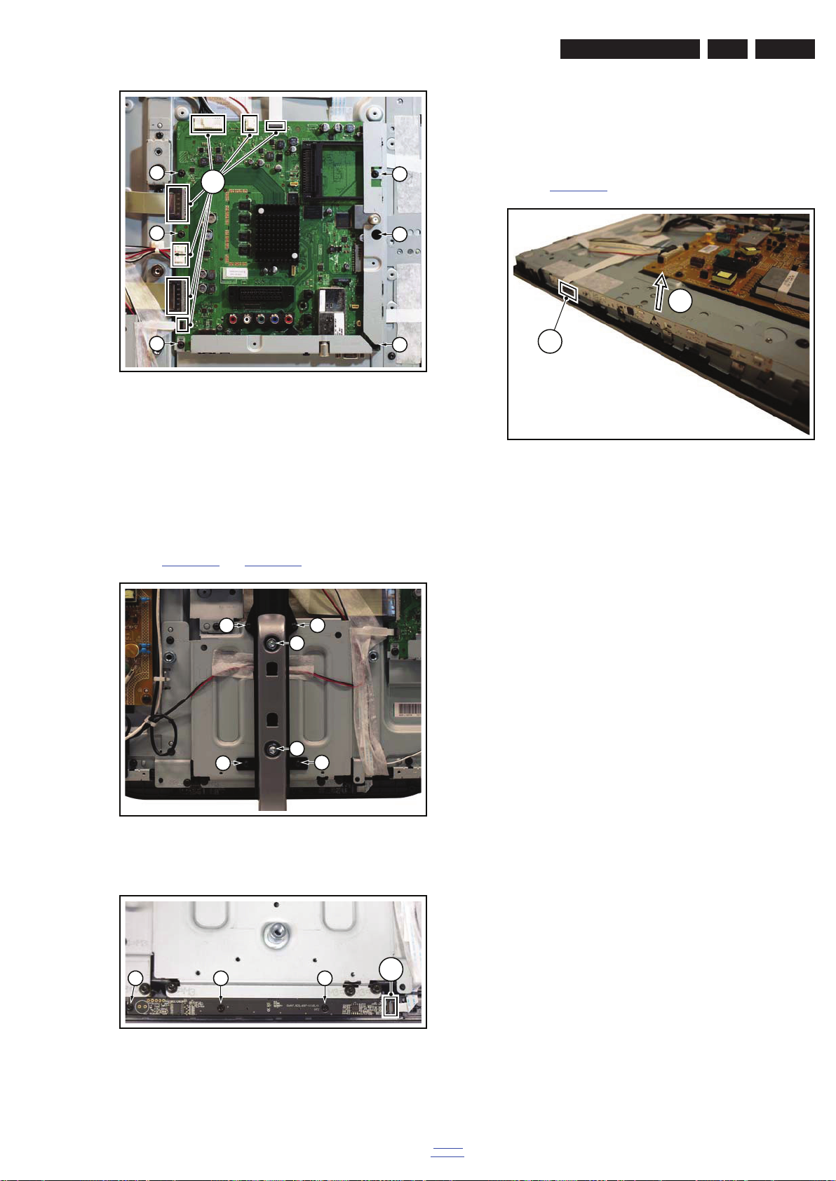
Figure 4-20 SSB
19100_051_110216.eps
110216
2
2
2
2
2
2
1
19100_052_110216.eps
110216
1
1
1
1
1
1
19100_053_110216.eps
110216
2
2 2
3
19100_054_110216.eps
110216
1. Unplug all connectors [1].
2. Remove the fixation screws [2].
3. Take the board out.
When remounting, ensure that the side shielding is positioned
correctly.
4.4.6 Keyboard Control, IR & LED Board
Refer to Figure 4-21
and Figure 4-22 for details.
Mechanical Instructions
3. Remove the screws [3] and take the board out.
When defective, replace the whole unit.
4.4.7 Ambilight Units
The Ambilight units can be lifted from the subframes without
the use of tools.
Refer to Figure 4-23
1. Unplug the connector [1].
2. Carefully lift the board [2] and take the board out.
When defective, replace the whole unit.
EN 19Q552.2L LA 4.
for details.
2
1
Figure 4-23 Ambilight units
Figure 4-21 Keyboard control, IR & LED board [1/2]
Figure 4-22 Keyboard control, IR & LED board [2/2]
1. Remove the stand and the plastic support [1].
2. Unplug the connector [2].
back to
div. table
2011-Jul-15
Page 20
EN 20 Q552.2L LA4.
19100_055_110216.eps
110216
4
4
4 4 4 4
4
2
2
2
2
2
1
19100_056_110217.eps
110217
4
4.4.8 LCD Panel
Mechanical Instructions
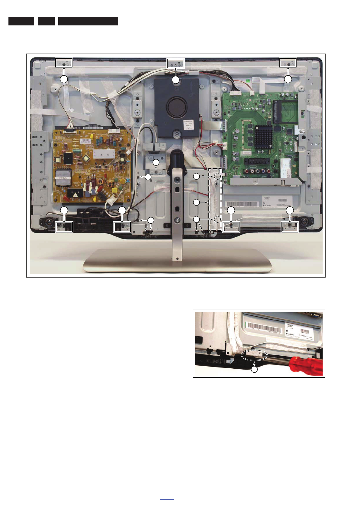
Refer to Figure 4-24
and Figure 4-25 for details.
Figure 4-24 LCD panel [1/2]
1. Remove the SSB as described earlier.
2. Remove the PSU as described earlier.
3. Remove the tweeters with their subframes and subwoofer
as described earlier.
4. Remove the stand and -support as described earlier.
5. Remove the cables [1].
6. Remove the stand subframe [2].
7. Remove the mains switch subframe [3].
8. Remove the Ambilight units together with their subframes
as described earlier.
9. Unplug the connector from the keyboard control-, and IR &
LED board as described earlier.
10. Remove all remaining cables and subframes.
11. Use a screwdriver to release the clamps [4] that secure the
panel and take the panel out.
Remove the clamps from the panel before sending the panel in
for Service.
Figure 4-25 LCD panel [2/2]
2011-Jul-15
back to
div. table
Page 21

4.5 Set Re-assembly
To re-assemble the whole set, execute all processes in reverse
order.
Notes:
• While re-assembling, make sure that all cables are placed
and connected in their original position.
• Pay special attention not to damage the EMC foams in the
set. Ensure that EMC foams are mounted correctly.
Mechanical Instructions
EN 21Q552.2L LA 4.
back to
div. table
2011-Jul-15
Page 22
EN 22 Q552.2L LA5.
19100_057_110217.eps
110217
SDM
Service Modes, Error Codes, and Fault Finding
5. Service Modes, Error Codes, and Fault Finding
Index of this chapter:
5.1 Test Points
5.2 Service Modes
5.3 Stepwise Start-up
5.4 Service Tools
5.5 Error Codes
5.6 The Blinking LED Procedure
5.7 Protections
5.8 Fault Finding and Repair Tips
5.9 Software Upgrading
5.1 Test Points
As most signals are digital, it will be difficult to measure
waveforms with a standard oscilloscope. However, several key
ICs are capable of generating test patterns, which can be
controlled via ComPair. In this way it is possible to determine
which part is defective.
Perform measurements under the following conditions:
• Service Default Mode.
• Video: Color bar signal.
• Audio: 3 kHz left, 1 kHz right.
5.2 Service Modes
Service Default mode (SDM) and Service Alignment Mode
(SAM) offers several features for the service technician, while
the Customer Service Mode (CSM) is used for communication
between the call centre and the customer.
• All service-unfriendly modes (if present) are disabled, like:
– (Sleep) timer.
– Child/parental lock.
– Picture mute (blue mute or black mute).
– Automatic volume levelling (AVL).
– Skip/blank of non-favorite pre-sets.
How to Activate SDM
For this chassis there are two kinds of SDM: an analogue SDM
and a digital SDM. Tuning will happen according Table 5-1
• Analogue SDM: use the standard RC-transmitter and key
in the code “062596”, directly followed by the “MENU” (or
“HOME”) button.
Note: It is possible that, together with the SDM, the main
menu will appear. To switch it “off”, push the “MENU” (or
"HOME") button again.
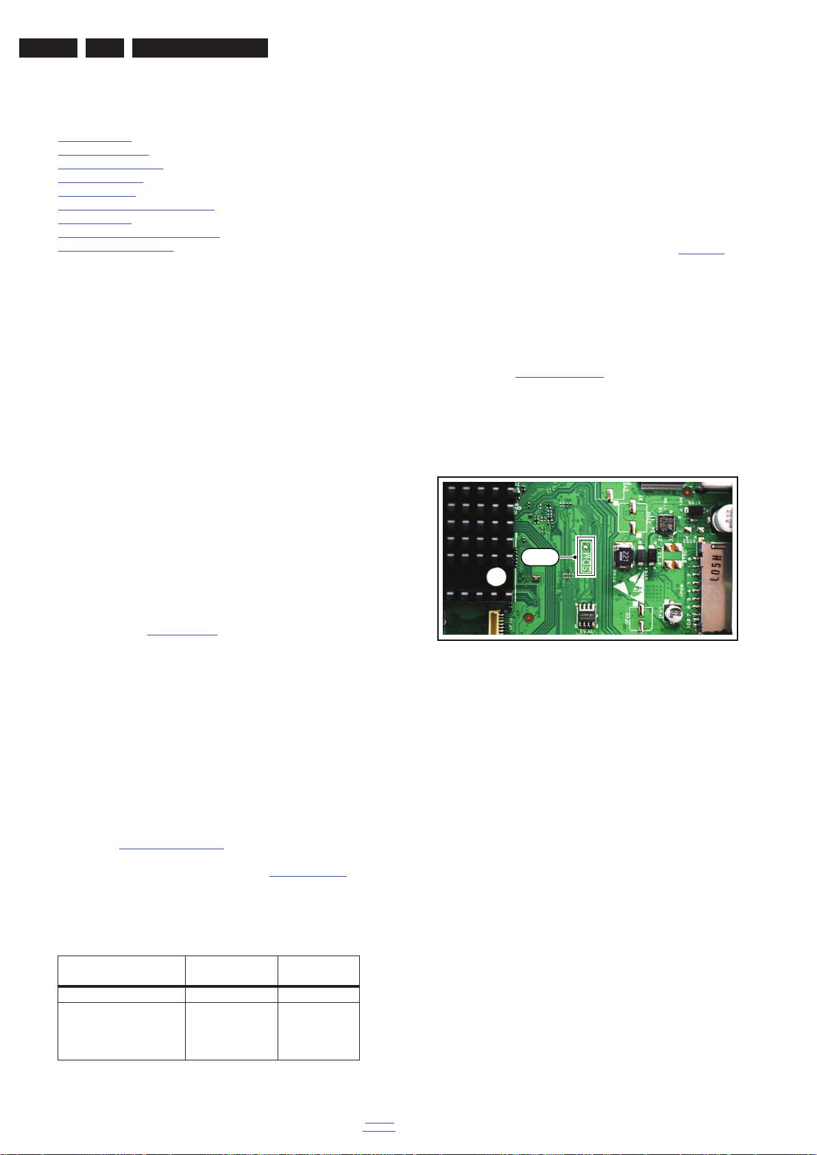
Analogue SDM can also be activated by grounding for a
moment the solder path on the SSB, with the indication
“SDM” (see Service mode pad
• Digital SDM: use the standard RC-transmitter and key in
the code “062593”, directly followed by the “MENU” (or
"HOME") button.
Note: It is possible that, together with the SDM, the main
menu will appear. To switch it “off”, push the “MENU” (or
"HOME") button again.
).
.
This chassis also offers the option of using ComPair, a
hardware interface between a computer and the TV chassis. It
offers the abilities of structured troubleshooting, error code
reading, and software version read-out for all chassis.
(see also section “5.4.1 ComPair
Note: For the new model range, a new remote control (RC) is
used with some renamed buttons. This has an impact on the
activation of the Service modes. For instance the old “MENU”
button is now called “HOME” (or is indicated by a “house” icon).
5.2.1 Service Default Mode (SDM)
Purpose
• To create a pre-defined setting, to get the same
measurement results as given in this manual.
• To override SW protections detected by stand-by
processor and make the TV start up to the step just before
protection (a sort of automatic stepwise start-up). See
section “5.3 Stepwise Start-up
• To start the blinking LED procedure where only LAYER 2
errors are displayed. (see also section “5.5 Error Codes
Specifications
Table 5-1 SDM default settings
Region Freq. (MHz)
Europe, AP(PAL/Multi) 475.25 PAL B/G
Europe, AP DVB-T 546.00 PID
• All picture settings at 50% (brightness, color, contrast).
• Sound volume at 25%.
2011-Jul-15
”).
”.
Video: 0B 06 PID
PCR: 0B 06 PID
Audio: 0B 07
Default
system
DVB-T
”).
Figure 5-1 Service mode pad
After activating this mode, “SDM” will appear in the upper right
corner of the screen (when a picture is available).
How to Navigate
When the “MENU” (or “HOME”) button is pressed on the RC
transmitter, the TV set will toggle between the SDM and the
normal user menu.
How to Exit SDM
Use one of the following methods:
• Switch the set to STAND-BY via the RC-transmitter.
• Via a standard customer RC-transmitter: key in “00”sequence.
5.2.2 Service Alignment Mode (SAM)
Purpose
• To perform (software) alignments.
• To change option settings.
• To easily identify the used software version.
• To view operation hours.
• To display (or clear) the error code buffer.
How to Activate SAM
Via a standard RC transmitter: Key in the code “062596”
directly followed by the “INFO” or “OK” button. After activating
SAM with this method a service warning will appear on the
screen, continue by pressing the “OK” button on the RC.
back to
div. table
Page 23
10000_038_090121.eps
090819
PHILIPS
MODEL:
32PF9968/10
PROD.SERIAL NO:
AG 1A0620 000001
040
39mm
27mm
(CTN Sticker)
Display Option
Code
Service Modes, Error Codes, and Fault Finding
EN 23Q552.2L LA 5.
Contents of SAM
• Hardware Info.
– A. SW Version. Displays the software version of the
main software (example: Q555X-1.2.3.4 =
AAAAB_X.Y.W.Z).
• AAAA= the chassis name.
• B= the SW branch version. This is a sequential
number (this is no longer the region indication, as
the software is now multi-region).
• X.Y.W.Z= the software version, where X is the
main version number (different numbers are not
compatible with one another) and Y.W.Z is the sub
version number (a higher number is always
compatible with a lower number).
– B. STBY PROC Version. Displays the software
version of the stand-by processor.
– C. Production Code. Displays the production code of
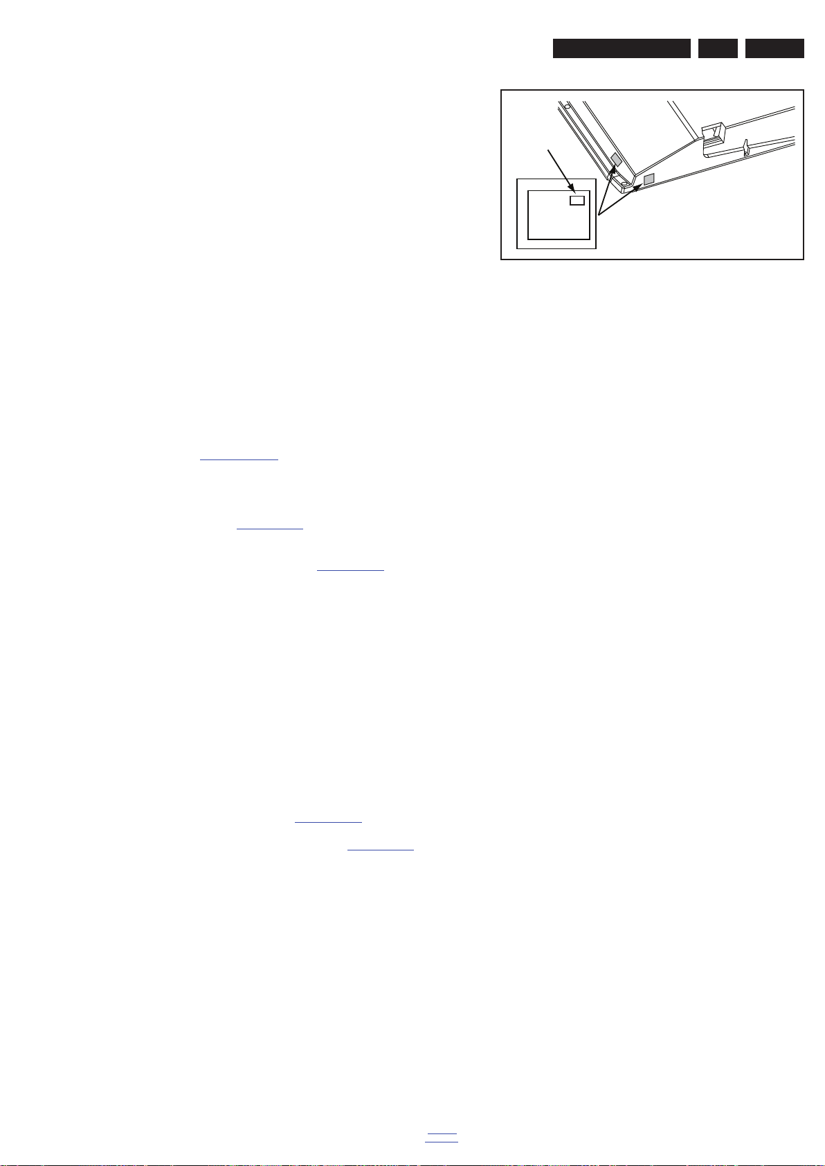
Figure 5-2 Location of Display Option Code sticker
the TV, this is the serial number as printed on the back
of the TV set. Note that if an NVM is replaced or is
initialized after corruption, this production code has to
be re-written to NVM. ComPair will foresee in a
possibility to do this.
• Operation Hours. Displays the accumulated total of
operation hours (not the stand-by hours). Every time the
TV is switched “on/off”, 0.5 hours is added to this number.
• Errors (followed by maximum 10 errors). The most recent
error is displayed at the upper left (for an error explanation
see section “5.5 Error Codes
”).
• Reset Error Buffer. When “cursor right” (or “OK” button)
pressed here, followed by the “OK” button, the error buffer
is reset.
• Alignments. This will activate the “ALIGNMENTS” submenu. See Chapter 6. Alignments
.
• Dealer Options. Extra features for the dealers.
• Options. Extra features for Service. For more info
regarding option codes, see chapter 6. Alignments
.
Note that if the option code numbers are changed, these
have to be confirmed with pressing the “OK” button before
the options are stored, otherwise changes will be lost.
• Initialize NVM. The moment the processor recognizes a
corrupted NVM, the “initialize NVM” line will be highlighted.
Now, two things can be done (dependent of the service
instructions at that moment):
– Save the content of the NVM via ComPair for
development analysis, before initializing. This will give
the Service department an extra possibility for
diagnosis (e.g. when Development asks for this).
– Initialize the NVM.
• Store - go right. All options and alignments are stored
when pressing “cursor right” (or the “OK” button) and then
the “OK”-button.
• Operation hours display. Displays the accumulated total
of operation hours of the screen itself. In case of a display
replacement, reset to “0” or to the consumed operation
hours of the spare display.
• SW Maintenance.
– SW Events. In case of specific software problems, the
development department can ask for this info.
– HW Events. In case of specific software problems, the
development department can ask for this info :
- Event 26: refers to a power dip, this is logged after
the TV set reboots due to a power dip.
- Event 17: refers to the power OK status, sensed even
before the 3 x retry to generate the error code.
• Test settings. For development purposes only.
• Development file versions. Not useful for Service
purposes, this information is only used by the development
department.
• Upload to USB. To upload several settings from the TV to
an USB stick, which is connected to the SSB. The items are
“Channel list”, “Personal settings”, “Option codes”,
“Alignments”, “Identification data” (includes the set type
and prod code + all 12NC like SSB, display, boards),
“History list”. The “All” item supports to upload all several
items at once.
First a directory “repair\” has to be created in the root
of the USB stick.
To upload the settings, select each item separately, press
“cursor right” (or the “OK” button), confirm with “OK” and
Note: When the NVM is corrupted, or replaced, there is a high
possibility that no picture appears because the display code is
not correct. So, before initializing the NVM via the SAM, a
picture is necessary and therefore the correct display option
has to be entered. Refer to Chapter 6. Alignments
for details.
To adapt this option, it’s advised to use ComPair (the correct
values for the options can be found in Chapter 6. Alignments
or a method via a standard RC (described below).
Changing the display option via a standard RC: Key in the
code “062598” directly followed by the “MENU” (or "HOME")
button and “XXX” (where XXX is the 3 digit decimal display
code as mentioned on the sticker in the set). Make sure to key
in all three digits, also the leading zero’s. If the above action is
successful, the front LED will go out as an indication that the
RC sequence was correct. After the display option is changed
in the NVM, the TV will go to the Stand-by mode. If the NVM
was corrupted or empty before this action, it will be initialized
first (loaded with default values). This initializing can take up to
20 seconds.
)
wait until the message “Done” appears. In case the
download to the USB stick was not successful, “Failure” will
be displayed. In this case, check if the USB stick is
connected properly and if the directory “repair” is present in
the root of the USB stick. Now the settings are stored onto
the USB stick and can be used to download into another TV
or other SSB. Uploading is of course only possible if the
software is running and preferably a picture is available.
This method is created to be able to save the customer’s
TV settings and to store them into another SSB.
• Download from USB. To download several settings from
the USB stick to the TV, same way of working needs to be
followed as described in “Upload to USB”. To make sure
that the download of the channel list from USB to the TV is
executed properly, it is necessary to restart the TV and
tune to a valid preset if necessary. The “All” item supports
to download all several items at once.
• NVM editor. For NET TV the set “type number” must be
entered correctly.
Also the production code (AG code) can be entered here
via the RC-transmitter.
Correct data can be found on the side/rear sticker.
back to
div. table
2011-Jul-15
Page 24

EN 24 Q552.2L LA5.
Service Modes, Error Codes, and Fault Finding
How to Navigate
• In SAM, the menu items can be selected with the
“CURSOR UP/DOWN” key on the RC-transmitter. The
selected item will be highlighted. When not all menu items
fit on the screen, move the “CURSOR UP/DOWN” key to
display the next/previous menu items.
• With the “CURSOR LEFT/RIGHT” keys, it is possible to:
– (De) activate the selected menu item.
– (De) activate the selected sub menu.
• With the “OK” key, it is possible to activate the selected
action.
How to Exit SAM
Use one of the following methods:
• Switch the TV set to STAND-BY via the RC-transmitter.
• Via a standard RC-transmitter, key in “00” sequence, or
select the “BACK” key.
5.2.3 Customer Service Mode (CSM)
Purpose
When a customer is having problems with his TV-set, he can
call his dealer or the Customer Helpdesk. The service
technician can then ask the customer to activate the CSM, in
order to identify the status of the set. Now, the service
technician can judge the severity of the complaint. In many
cases, he can advise the customer how to solve the problem,
or he can decide if it is necessary to visit the customer.
The CSM is a read only mode; therefore, modifications in this
mode are not possible.
When in this chassis CSM is activated, a test pattern will be
displayed during 5 seconds (1 second Blue, 1 second Green
and 1 second Red, then again 1 second Blue and 1 second
Green). This test pattern is generated by the PNX51X0
(located on the 200Hz board as part of the display). So if this
test pattern is shown, it could be determined that the back end
video chain (PNX51X0 and display) is working.For TV sets
without the PNX51X0 inside, every menu from CSM will be
used as check for the back end chain video.
When CSM is activated and there is a USB stick connected to
the TV set, the software will dump the CSM content to the USB
stick. The file (CSM_model number_serial number.txt) will be
saved in the root of the USB stick. This info can be handy if no
information is displayed.
When in CSM mode (and a USB stick connected), pressing
“OK” will create an extended CSM dump file on the USB stick.
This file (Extended_CSM_model number_serial number.txt)
contains:
• The normal CSM dump information,
• All items (from SAM “load to USB”, but in readable format),
• Operating hours,
• Error codes,
• SW/HW event logs.
To have fast feedback from the field, a flashdump can be
requested by development. When in CSM, push the “red”
button and key in serial digits ‘2679’ (same keys to form the
word ‘COPY’ with a cellphone). A file “Dump_model
number_serial number.bin” will be written on the connected
USB device. This can take 1/2 minute, depending on the
quantity of data that needs to be dumped.
Also when CSM is activated, the LAYER 1 error is displayed via
blinking LED. Only the latest error is displayed (see also
section 5.5 Error Codes
).
How to Activate CSM
Key in the code “123654” via the standard RC transmitter.
Note: Activation of the CSM is only possible if there is no (user)
menu on the screen!
How to Navigate
By means of the “CURSOR-DOWN/UP” knob on the RCtransmitter, can be navigated through the menus.
Contents of CSM
The contents are reduced to 3 pages: General, Software
versions and Quality items. The group names itself are not
shown anywhere in the CSM menu.
General
• Set Type. This information is very helpful for a helpdesk/
workshop as reference for further diagnosis. In this way, it
is not necessary for the customer to look at the rear of the
TV-set. Note that if an NVM is replaced or is initialized after
corruption, this set type has to be re-written to NVM.
ComPair will foresee in a possibility to do this. The update
can also be done via the NVM editor available in SAM.
• Production Code. Displays the production code (the serial
number) of the TV. Note that if an NVM is replaced or is
initialized after corruption, this production code has to be
re-written to NVM. ComPair will foresee in a possibility to
do this. The update can also be done via the NVM editor
available in SAM.
• Installed date. Indicates the date of the first installation of
the TV. This date is acquired via time extraction.
• Options 1. Gives the option codes of option group 1 as set
in SAM (Service Alignment Mode).
• Options 2. Gives the option codes of option group 2 as set
in SAM (Service Alignment Mode).
• 12NC SSB. Gives an identification of the SSB as stored in
NVM. Note that if an NVM is replaced or is initialized after
corruption, this identification number has to be re-written to
NVM. ComPair will foresee in a possibility to do this. This
identification number is the 12nc number of the SSB.
• 12NC display. Shows the 12NC of the display.
• 12NC supply. Shows the 12NC of the power supply.
• 12NC 200Hz board. Shows the 12NC of the 200Hz Panel
(when present).
• 12NC AV PIP. Shows the 12NC of the AV PIP board
(when present).
Software versions
• Current main SW. Displays the build-in main software
version. In case of field problems related to software,
software can be upgraded. As this software is consumer
upgradeable, it will also be published on the Internet.
Example: Q55xx1.2.3.4
• Stand-by SW. Displays the build-in stand-by processor
software version. Upgrading this software will be possible
via ComPair or via USB (see section 5.9 Software
Upgrading).
Example: STDBY_83.84.0.0.
• e-UM version. Displays the electronic user manual SWversion (12NC version number). Most significant number
here is the last digit.
• AV PIP software.
• 3D dongle software version.
Quality items
• Signal quality. Bad / average /good (not for DVB-S).
• Ethernet MAC address. Displays the MAC address
present in the SSB.
• Wireless MAC address. Displays the wireless MAC
address to support the Wi-Fi functionality.
• BDS key. Indicates if the set is in the BDS status.
• CI module. Displays status if the common interface
module is detected.
• CI + protected service. Yes/No.
• Event counter :
S : 000X 0000(number of software recoveries : SW
EVENT-LOG #(reboots)
S : 0000 000X (number of software events : SW EVENTLOG #(events)
H : 000X 0000(number of hardware errors)
2011-Jul-15
back to
div. table
Page 25
Service Modes, Error Codes, and Fault Finding
18770_250_100216.eps
100402
Active
Semi
St by
St by
Mains
on
Mains
off
GoToProtection
- WakeUp requested
- Acquisition needed
- Tact switch pushed
- stby requested and
no data Acquisition
required
- St by requested
- tact SW pushed
WakeUp
requested
Protection
WakeUp
requested
(SDM)
GoToProtection
Hibernate
- Tact switch pushed
- last status is hibernate
after mains ON
Tact switch
pushed
EN 25Q552.2L LA 5.
H : 0000 000X (number of hardware events : SW EVENTLOG #(events).
How to Exit CSM
Press “MENU” (or "HOME") / “Back” key on the RC-transmitter.
5.3 Stepwise Start-up
When the TV is in a protection state due to an error detected by
stand-by software (error blinking is displayed) and SDM is
activated via shortcutting the SDM solder path on the SSB, the
TV starts up until it reaches the situation just before protection.
So, this is a kind of automatic stepwise start-up. In combination
with the start-up diagrams below, you can see which supplies
are present at a certain moment. Caution: in case the start-up
in this mode with a faulty FET 7U0X is done, you can destroy
all IC’s supplied by the +1V8 and +1v1, due to overvoltage (12V
on XVX-line). It is recommended to measure first the FET
7U0X or others FET’s on shortcircuit before activating SDM via
the service pads.
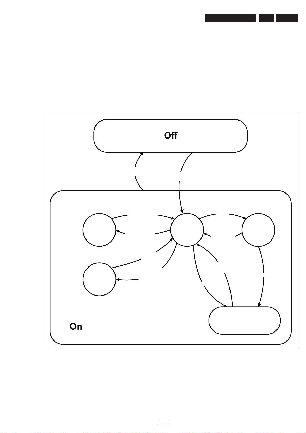
The abbreviations “SP” and “MP” in the figures stand for:
• SP: protection or error detected by the Stand-by
Processor.
• MP: protection or error detected by the MIPS Main
Processor.
Figure 5-3 Transition diagram
back to
div. table
2011-Jul-15
Page 26
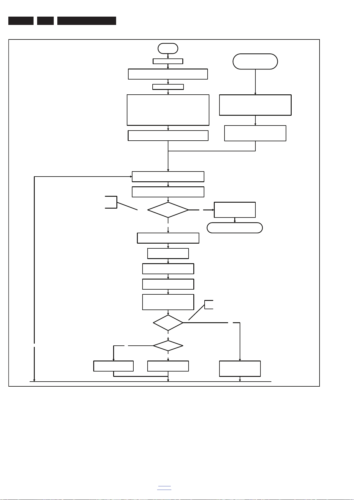
EN 26 Q552.2L LA5.
Service Modes, Error Codes, and Fault Finding
Off
Mains is applied
Stand by or
Protection
Standby Supply starts running.
All standby supply voltages become available.
st-by μP resets
Detect2 is moved to an interrupt. To be checked if
the detection on interrupt base is feasible or not or if
we should stick to the standard 40ms interval.
Initialise I/O pins of the st-by μP:
- Switch reset-AVC LOW (reset state)
- Switch reset-system LOW (reset state)
- Switch reset-Ethernet LOW (reset state)
- Switch reset-USB LOW (reset state)
- Switch reset-DVBs LOW (reset state)
- keep Audio-reset and Audio-Mute-Up HIGH
start keyboard scanning, RC detection. Wake up reasons are
Switch ON Platform and display supply by switching
+12V, +24Vs, AL and Bolt-on power
is switched on, followed by the +1V2 DCDC converter
Enable the supply detection algorithm
off.
LOW the Standby line.
Detect2 high received
within 2 seconds?
Yes
Enable the DCDC converter s
(ENABLE-3V3n LOW)
Wait 50ms
No
If the protection state was left by short circuiting the
SDM pins, detection of a protection condition during
startup will stall the startup. Protection conditions in a
playing set will be ignored. The protection mode will
not be entered.
- Switch Audio-Reset high.
It is low in the standby mode if the standby
mode lasted longer than 10s.
12V error :
Layer1: 3
Layer2: 16
Enter protection
Set I²C slave address
of Standby μP to (A0h)
Detect EJTAG debug probe
(pulling pin of the probe interface to
ground by inserting EJTAG probe)
EJTAG probe
connected ?
No
No
Release AVC system reset
Feed warm boot script
No
Cold boot?
Yes
Release AVC system reset
Feed cold boot script
An EJTAG probe (e.g. WindPower ICE probe) can be
connected for Linux Kernel debugging purposes.
Yes
Release AVC system reset
Feed initializing boot script
disable alive mechanism
18770_251_100216.eps
100216
Figure 5-4 “Off” to “Semi Stand-by” flowchart (part 1)
2011-Jul-15
back to
div. table
Page 27
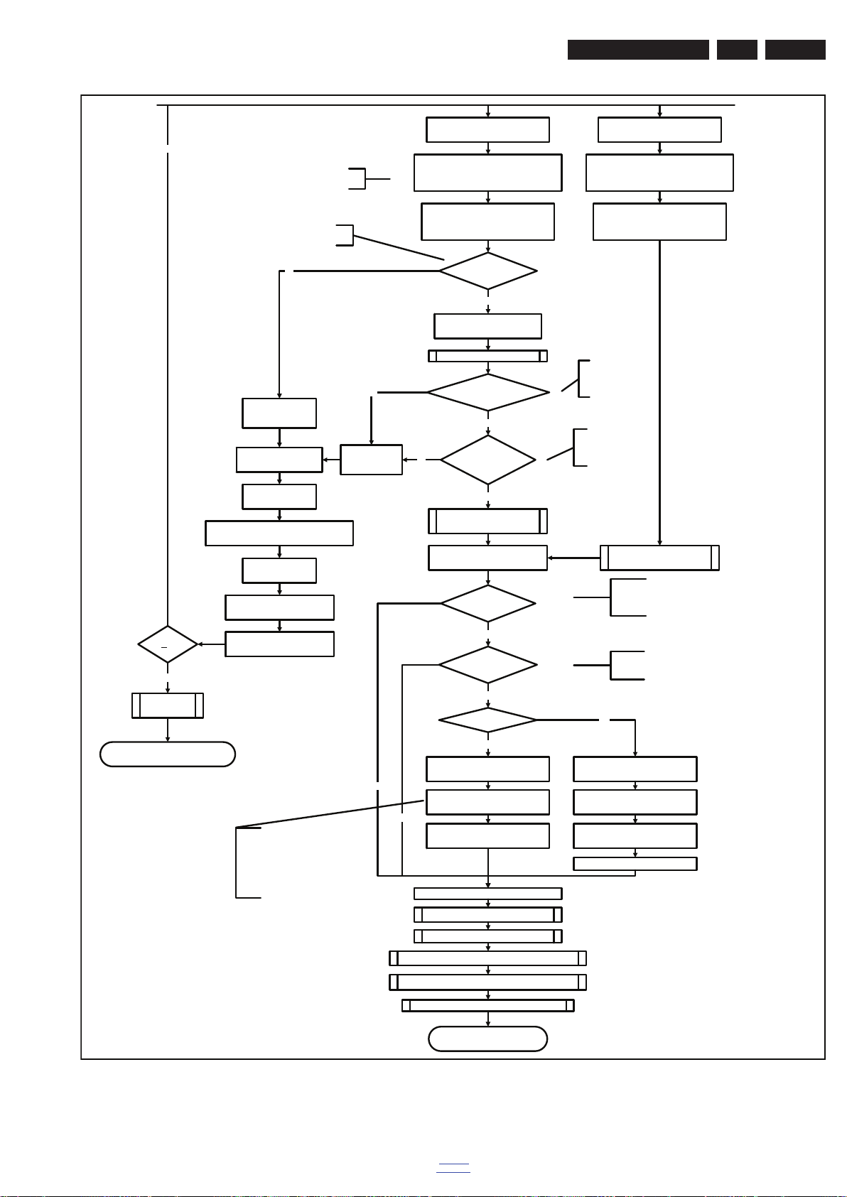
Service Modes, Error Codes, and Fault Finding
EN 27Q552.2L LA 5.
No
3-th try?
Yes
Blink Code as
error code
This cannot be done through the bootscript,
the I/O is on the sta ndby μP
Timing need to be updated if
more mature info is available.
No
Code =
Layer1: 2
Layer2: 15
Switch AVC PNX85500 in
reset (active low)
Wait 10ms
Disable all supply related protections and
switch off the +3V3 +5V DC/DC converter.
Wait 5ms
switch off the remaining DC/DC
converters
Switch Standby I/O line high
and wait 4 seconds
No
Code =
Layer1: 2
Layer2: 53
Reset-system is switched HIGH by the
AVC at the end of the bootscript
AVC releases Reset-Ethernet, Reset-USB and
Reset-DVBs when the end of the AVC boot-
script is detected
Reset-Audio and Audio-Mute-Up are
switched by MIPS code later on in the
startup process
Bootscript ready
in 1250 ms?
Yes
Set I²C slave address
of Standby μP to (60h)
RPC start (comm. protocol)
Flash to Ram
image transfer succeeded
within 30s?
Yes
No
SW initialization
succeeded
within 20s?
Yes
Enable Alive check mechanism
MIPS reads the wake up reason
from standby μP.
Wake up reason
coldboot & not semi-
standby?
yes
Startup screen cfg file
present?
yes
200Hz set?
Reset-system is switched HIGH by the
AVC at the end of the bootscript
AVC releases Reset-Ethernet, Reset-USB and
Reset-DVBs when the end of the AVC boot-
script is detected
Reset-Audio and Audio-Mute-Up are
switched by MIPS code later on in the
startup process
Timing needs to
be updated if more
mature info is
available.
Timing needs to be
updated if more
mature info is
available.
Wait until AVC starts to
communicat e
Startup screen shall only be visible when there is a coldboot to
an active state end situation. The startup screen shall not be
visible when waking up for reboot reasons or waking up to semistandby conditions or waking up to enter Hibernate mode. .
The first time after the option turn on o f the startup screen or
when the set is virgin, the cfg file is not present and hence
the startup screen will not be shown.
yes
Enter protection
To keep this flowchart readable, the exact
display turn on description is not copied
here. Please see the Semi-standby to On
description for the detailed display startup
During the complete display time of the
Startup screen, the preheat condition of
sequence.
100% PWM is valid.
Figure 5-5 “Off” to “Semi Stand-by” flowchart (part 2)
No
85500 sends out startup screen
No
85500 starts up the display.
No
Startup screen visible
Initialize audio
initialize tuner and channel decoders
Initialize source s election
Initialize video processing IC’s
initialize AutoTV by triggering CHS AutoTV Init interface
Initialize Ambilight with Lights off.
Semi-Standby
85500 sends out startup screen
200Hz Tcon has started up the
display.
85500 requests Lamp on
Startup screen visible
18770_252_100216.eps
100216
back to
div. table
2011-Jul-15
Page 28
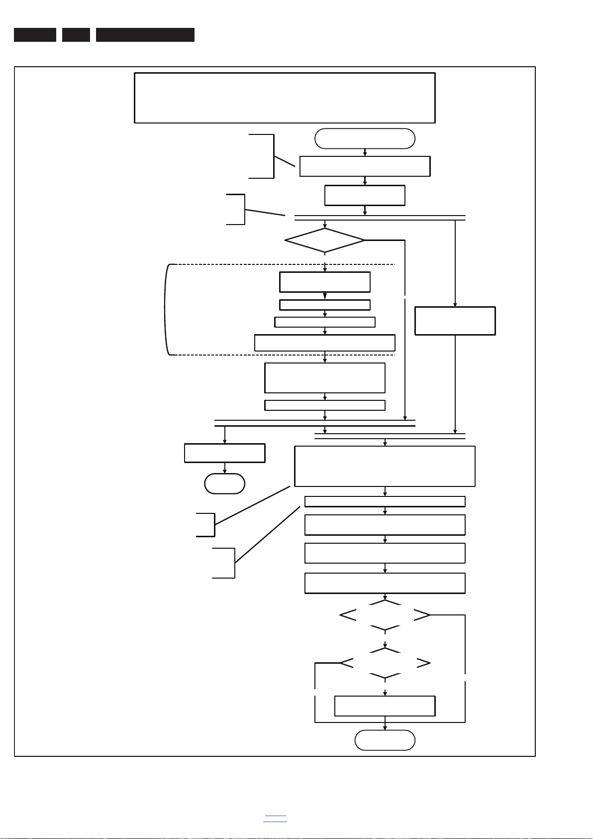
EN 28 Q552.2L LA5.
18770_253_100216.eps
100216
Active
Semi Standby
Initialize audio and video
processing IC's and functions
according needed use case.
Assert RGB video blanking
and audio mute
Wait until previous on-state is left more than 2
seconds ago. (to prevent LCD display problems)
The assumption here is that a fast toggle (<2s) can
only happen during ON->SEMI ->ON. In these states,
the AVC is still active and can provide the 2s delay. A
transition ON->SEMI->STBY->SEMI->ON cannot be
made in less than 2s, because the standby state will
be maintained for at least 4s.
Switch Audio-Reset low and wait 5ms
Constraints taken into account:
- Display may only be started when valid LVDS output clock can be delivered by the AVC.
- To have a reliable operation of the EEFL backlight, the backlight should be driven with a maximum PWM duty
cycle during the first seconds. Only after this first one or two seconds, the PWM may be set to the requir ed output
level (Note that the PWM output should be present before the backlight is switched on). To minimize the artefacts,
the picture should only be unblanked after these first seconds.
Restore dimming backlight feature, PWM and BOOST output
and unblank the video.
Wait until valid and stable audio and video, corresponding to the
requested output is delivered by the AVC
AND
the backlight has been switched on for at least the time which is
indicated in the display file as preheat time.
The higher level requirement is that audio and video
should be demuted without transient effects and that
the audio should be demuted maximum 1s before or
at the same time as the unblanking of the video.
Release audio mute and wait 100ms before any other audio
handling is done (e.g. volume change)
CPipe already generates a valid output
clock in the semi-standby state: display
startup can start immediately when leaving
the semi-standby state.
Switch on LCD backlight (Lamp-ON)
Switch off the dimming backlight feature, set
the BOOST control to nominal and make sure
PWM output is set to maximum allowed PWM
Switch on the Ambilight functionality according the last status
settings.
Delay Lamp-on with the sum of the LVDS delay and
the Lamp delay indicated in the display file
Switch on the display power by
switching LCD-PWR-ON low
Wait x ms
Switch on LVDS output in the 85500
No
The exact timings to
switch on the
display (LVDS
delay, lamp delay)
are defined in the
display file.
Start POK line
detection algorithm
return
Display already on?
(splash screen)
Yes
Display cfg file present
and up to date, according
correct display option?
Startup screen Option
and Installation setting
Photoscreen ON?
Yes
No
Prepare Start screen Display config
file and copy to Flash
No
Yes
A LED set does not normally need a
preheat time. The preheat remains present
but is set to zero in the display file.
Service Modes, Error Codes, and Fault Finding
Figure 5-6 “Semi Stand-by” to “Active” flowchart (EEFL or LED backlight 50/100 Hz only)
2011-Jul-15
back to
div. table
Page 29
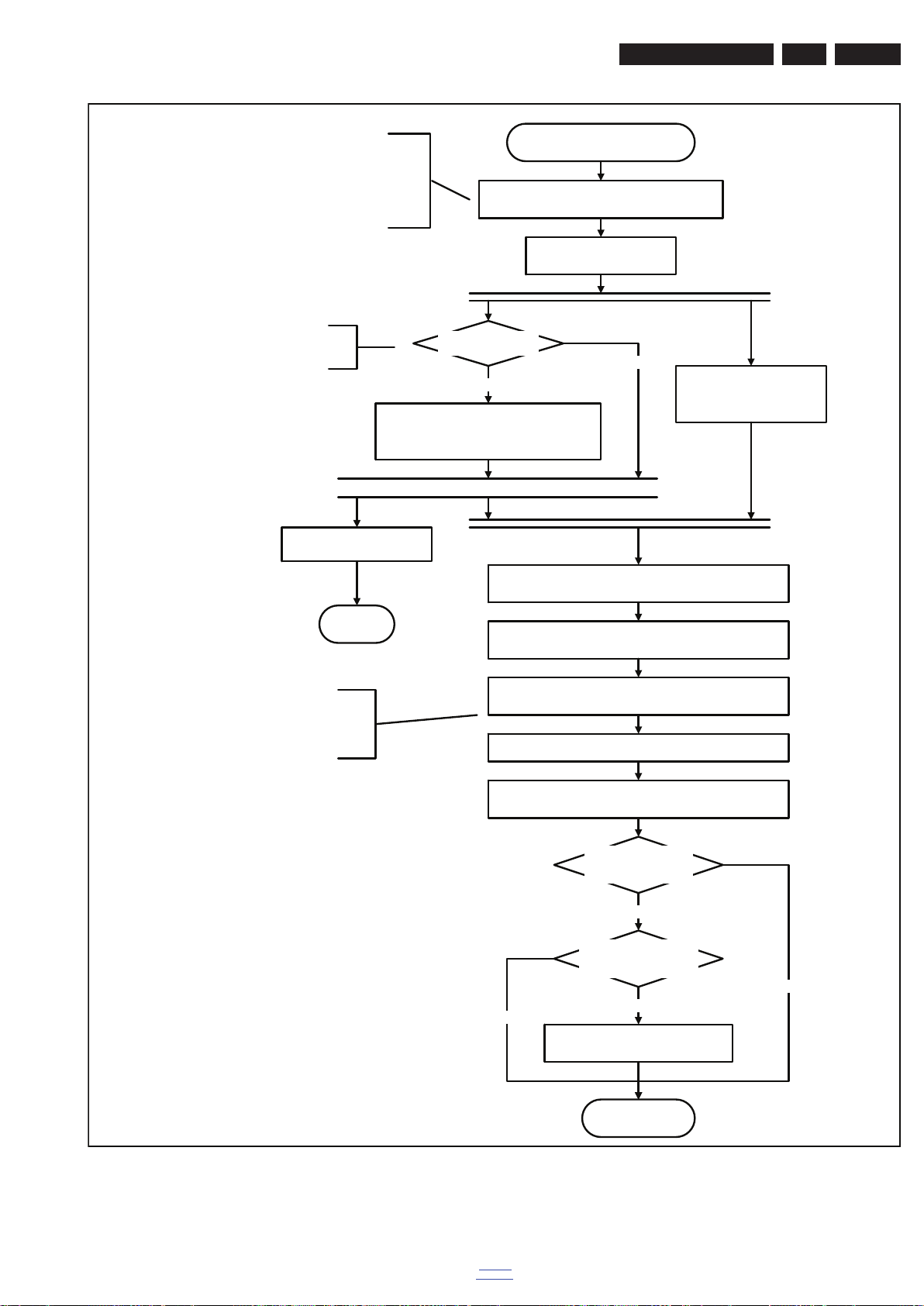
Service Modes, Error Codes, and Fault Finding
18770_254_100216.eps
100216
Active
Semi Standby
Initialize audio and video
processing IC's and functions
according needed use case.
Assert RGB video blanking
and audio mute
Wait until previous on-state is left more than 2
seconds ago. (to prevent LCD display problems)
The assumption here is that a fast toggle (<2s)
can only happen during ON->SEMI ->ON. In
these states, the AVC is still active and can
provide the 2s delay. If the transition ON->SEMI>STBY->SEMI->ON can be made in less than 2s,
we have to delay the semi -> stby transition until
the requirement is met.
Switch Audio-Reset low and wait 5ms
unblank the video.
Wait until valid and stable audio and video, corresponding to
the requested output is delivered by the AVC.
The higher level requirement is that audio and
video should be demuted without transient
effects and that the audio should be demuted
maximum 1s before or at the same time as the
unblanking of the video.
Release audio mute and wait 100ms before any other audio
handling is done (e.g. volume change)
Request Tcon to Switch on the backlight in a
direct LED or
set Lamp-on I/O line in case of a side LED
Switch on the Ambilight functionality according the last status
settings.
There is no need to define the
display timings since the timing
implementation is part of the Tcon.
Start POK line
detection algorithm
return
Display cfg file present
and up to date, according
correct display option?
Startup screen Option
and Installation setting
Photoscreen ON?
Yes
No
Prepare Start screen Display config
file and copy to Flash
No
Yes
Backlight already on?
(splash screen)
No
Yes
EN 29Q552.2L LA 5.
Figure 5-7 “Semi Stand-by” to “Active” flowchart (LED backlight 200 Hz)
back to
div. table
2011-Jul-15
Page 30
EN 30 Q552.2L LA5.
Service Modes, Error Codes, and Fault Finding
Active
Mute all sound outputs via softmute
Wait 100ms
Set main amplifier mute (I/O: audio-mute)
Force ext audio outputs to ground
(I/O: audio reset)
And wait 5ms
switch off Ambilight
Yes
Instruct 200Hz
Tcon to turn off
the display
Wait until Ambilight has faded out: Output power
Observer should be zero
Switch off POK line
detection algorithm
switch off LCD backlight
(I/O or I²C)
Mute all video outputs
200Hz set?
No
Wait x ms (display file)
Switch off LVDS output in 85500
Wait x ms
Switch off the display power by
switching LCD-PWR-ON high
The exact timings to
switch off the
display (LVDS
delay, lamp delay)
are defined in the
display file.
2011-Jul-15
Semi Standby
Figure 5-8 “Active” to “Semi Stand-by” flowchart
back to
div. table
18770_255_100216.eps
100216
Page 31
Service Modes, Error Codes, and Fault Finding
Semi Stand by
If ambientlight functionality was used in semi-standby
(lampadaire mode), switch off ambient light (see CHS
ambilight)
EN 31Q552.2L LA 5.
Delay transition until ramping down of ambient light is
finished. *)
transfer Wake up reasons to the Stand by μP.
Switch Memories to self-refresh (this creates a more
stable condition when switching off the power).
Switch AVC system in reset state (reset-system and
reset-AVC lines)
Switch reset-USB, Reset-Ethernet and Reset-DVBs
LOW
Wait 10ms
Disable all supply related protections and switch off
the DC/DC converters (ENABLE-3V3n)
Wait 5ms
Switch OFF all supplies by switching HIGH the
Standby I/O line
*) If this is not performed and the set is
switched to standby when the switch off of
the ambilights is still ongoing, the lights will
switch off abruptly when the supply is cut.
Important remarks:
release reset audio 10 sec after entering
standby to save power
Also here, the standby state has to be
maintained for at least 4s before starting
another state transition.
Stand by
Figure 5-9 “Semi Stand-by” to “Stand-by” flowchart
back to
div. table
18770_256_100216.eps
100216
2011-Jul-15
Page 32
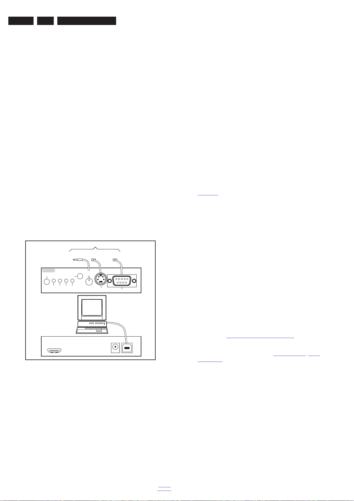
EN 32 Q552.2L LA5.
10000_036_090121.eps
091118
TO
UART SERVICE
CONNECTOR
TO
UART SERVICE
CONNECTOR
TO
I2C SERVICE
CONNECTOR
TO TV
PC
HDMI
I
2
C only
Optional power
5V DC
ComPair II Developed by Philips Brugge
RC out
RC in
Optional
Switch
Power ModeLink/
Activity
I
2
C
ComPair II
Multi
function
RS232 /UART
Service Modes, Error Codes, and Fault Finding
5.4 Service Tools
5.4.1 ComPair
Introduction
ComPair (Computer Aided Repair) is a Service tool for Philips
Consumer Electronics products. and offers the following:
1. ComPair helps to quickly get an understanding on how to
repair the chassis in a short and effective way.
2. ComPair allows very detailed diagnostics and is therefore
capable of accurately indicating problem areas. No
knowledge on I
because ComPair takes care of this.
3. ComPair speeds up the repair time since it can
automatically communicate with the chassis (when the μP
is working) and all repair information is directly available.
4. ComPair features TV software up possibilities.
Specifications
ComPair consists of a Windows based fault finding program
and an interface box between PC and the (defective) product.
The ComPair II interface box is connected to the PC via an
USB cable. For the TV chassis, the ComPair interface box and
the TV communicate via a bi-directional cable via the service
connector(s).
The ComPair fault finding program is able to determine the
problem of the defective television, by a combination of
automatic diagnostics and an interactive question/answer
procedure.
How to Connect
This is described in the chassis fault finding database in
ComPair.
Figure 5-10 ComPair II interface connection
Caution: It is compulsory to connect the TV to the PC as
shown in the picture above (with the ComPair interface in
between), as the ComPair interface acts as a level shifter. If
one connects the TV directly to the PC (via UART), ICs can be
blown!
How to Order
ComPair II order codes:
• ComPair II interface: 3122 785 91020.
• Software is available via the Philips Service web portal.
• ComPair UART interface cable for Q55x.x.
(using 3.5 mm Mini Jack connector): 3138 188 75051.
Note: When you encounter problems, contact your local
support desk.
2011-Jul-15
2
C or UART commands is necessary,
5.5 Error Codes
5.5.1 Introduction
The error code buffer contains all detected errors since the last
time the buffer was erased. The buffer is written from left to
right, new errors are logged at the left side, and all other errors
shift one position to the right.
When an error occurs, it is added to the list of errors, provided
the list is not full. When an error occurs and the error buffer is
full, then the new error is not added, and the error buffer stays
intact (history is maintained).
To prevent that an occasional error stays in the list forever, the
error is removed from the list after more than 50 hrs. of
operation.
When multiple errors occur (errors occurred within a short time
span), there is a high probability that there is some relation
between them.
New in this chassis is the way errors can be displayed:
• If no errors are there, the LED should not blink at all in
CSM or SDM. No spacer must be displayed as well.
• There is a simple blinking LED procedure for board
level repair (home repair) so called LAYER 1 errors
next to the existing errors which are LAYER 2 errors (see
Table 5-2
– LAYER 1 errors are one digit errors.
– LAYER 2 errors are 2 digit errors.
• In protection mode.
– From consumer mode: LAYER 1.
– From SDM mode: LAYER 2.
• Fatal errors, if I2C bus is blocked and the set reboots,
CSM and SAM are not selectable.
– From consumer mode: LAYER 1.
– From SDM mode: LAYER 2.
• In CSM mode.
– When entering CSM: error LAYER 1 will be displayed
• In SDM mode.
– When SDM is entered via Remote Control code or the
• Error display on screen.
– In CSM no error codes are displayed on screen.
– In SAM the complete error list is shown.
Basically there are three kinds of errors:
• Errors detected by the Stand-by software which lead to
protection. These errors will always lead to protection and
an automatic start of the blinking LED LAYER 1 error.
(see section “5.6 The Blinking LED Procedure
• Errors detected by the Stand-by software which not
lead to protection. In this case the front LED should blink
the involved error. See also section “5.5 Error Codes
Error Buffer”. Note that it can take up several minutes
before the TV starts blinking the error (e.g. LAYER 1
error = 2, LAYER 2 error = 15 or 53).
• Errors detected by main software (MIPS). In this case
the error will be logged into the error buffer and can be read
out via ComPair, via blinking LED method LAYER 1-2
error, or in case picture is visible, via SAM.
5.5.2 How to Read the Error Buffer
Use one of the following methods:
• On screen via the SAM (only when a picture is visible).
E.g.:
– 00 00 00 00 00: No errors detected
– 23 00 00 00 00: Error code 23 is the last and only
– 37 23 00 00 00: Error code 23 was first detected and
– Note that no protection errors can be logged in the
back to
div. table
).
by blinking LED. Only the latest error is shown.
hardware pins, LAYER 2 is displayed via blinking LED.
detected error.
error code 37 is the last detected error.
error buffer.
”).
, 5.5.4
Page 33
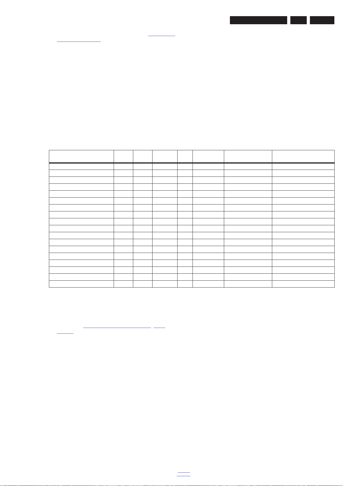
Service Modes, Error Codes, and Fault Finding
EN 33Q552.2L LA 5.
• Via the blinking LED procedure. See section 5.5.3 How to
Clear the Error Buffer.
•Via ComPair.
content, as this history can give significant information). This to
ensure that old error codes are no longer present.
If possible, check the entire contents of the error buffer. In
some situations, an error code is only the result of another error
5.5.3 How to Clear the Error Buffer
code and not the actual cause (e.g. a fault in the protection
detection circuitry can also lead to a protection).
Use one of the following methods:
• By activation of the “RESET ERROR BUFFER” command
in the SAM menu.
• If the content of the error buffer has not changed for 50+
hours, it resets automatically.
5.5.4 Error Buffer
In case of non-intermittent faults, clear the error buffer before
starting to repair (before clearing the buffer, write down the
There are several mechanisms of error detection:
• Via error bits in the status registers of ICs.
• Via polling on I/O pins going to the stand-by processor.
• Via sensing of analog values on the stand-by processor or
the PNX8550.
• Via a “not acknowledge” of an I
Take notice that some errors need several minutes before they
start blinking or before they will be logged. So in case of
problems wait 2 minutes from start-up onwards, and then
check if the front LED is blinking or if an error is logged.
Table 5-2 Error code overview
Monitored
Description Layer 1 Layer 2
2
I
C3 2 13 MIPS E BL / EB SSB SSB
2
C2 2 14 MIPS E BL / EB SSB SSB
I
2
C4 2 18 MIPS E BL / EB SSB SSB
I
by
Error/
Error Buffer/
Prot
Blinking LED Device Defective Board
PNX doesn’t boot (HW cause) 2 15 Stby μP P BL PNX8550 SSB
12V 3 16 Stby μP P BL / Supply
Inverter or display supply 3 17 MIPS E EB / Supply
PNX51X0 2/9 21 MIPS E EB PNX51X0 200 Hz board
HDMI mux 2 23 MIPS E EB Sil9x87A SSB
I2C switch 2 24 MIPS E EB PCA9540 SSB
Channel dec DVB-S 2 28 MIPS E EB STV0903 SSB
Lnb controller 2 31 MIPS E EB LNBH23 SSB
Tuner 2 34 MIPS E EB DTT 71300 SSB
Main nvm 2 35 MIPS E EB STM24C64 SSB
Tuner DVB-S 2 36 MIPS E EB STV6110 SSB
T° sensor SSB/set 2 42 MIPS E EB LM 75 T° sensor
T° sensor LED driver/Tcon 7 42 MIPS E EB LM 75 T° sensor
PNX doesn’t boot (SW cause) 2 53 Stby μP P BL PNX8550 SSB
Display 5 64 MIPS E BL / EB Altera Display
2
C communication.
Extra Info
• Rebooting. When a TV is constantly rebooting due to
internal problems, most of the time no errors will be logged
or blinked. This rebooting can be recognized via a ComPair
interface and Hyperterminal (for Hyperterminal settings,
see section “5.8 Fault Finding and Repair Tips
, 5.8.7
Logging). It’s shown that the loggings which are generated
by the main software keep continuing. In this case
diagnose has to be done via ComPair.
• Error 13 (I
2
C bus 3, SSB bus blocked). Current situation:
when this error occurs, the TV will constantly reboot due to
the blocked bus. The best way for further diagnosis here, is
to use ComPair.
• Error 14 (I
2
C bus 2, TV set bus blocked). Current
situation: when this error occurs, the TV will constantly
reboot due to the blocked bus. The best way for further
diagnosis here, is to use ComPair.
• Error 18 (I
2
C bus 4, Tuner bus blocked). In case this bus
is blocked, short the “SDM” solder paths on the SSB during
startup, LAYER error 2 = 18 will be blinked.
• Error 15 (PNX8550 doesn’t boot). Indicates that the main
processor was not able to read his bootscript. This error will
point to a hardware problem around the PNX8550
(supplies not OK, PNX 8550 completely dead, I
between PNX and Stand-by Processor broken, etc...).
When error 15 occurs it is also possible that I
blocked (NVM). I
2
C1 can be indicated in the schematics as
2
C link
2
C1 bus is
follows: SCL-UP-MIPS, SDA-UP-MIPS.
Other root causes for this error can be due to hardware
problems regarding the DDR’s and the bootscript reading
from the PNX8550.
• Error 16 (12V). This voltage is made in the power supply
and results in protection (LAYER 1 error = 3) in case of
absence. When SDM is activated we see blinking LED
LAYER 2 error = 16.
• Error 17 (Invertor or Display Supply). Here the status of
the “Power OK” is checked by software, no protection will
occur during failure of the invertor or display supply (no
picture), only error logging. LED blinking of LAYER 1
error = 3 in CSM, in SDM this gives LAYER 2 error = 17.
• Error 21 (PNX51X0). When there is no I
2
C communication
towards the PNX51X0 after start-up, LAYER 2 error = 21
will be logged and displayed via the blinking LED
procedure if SDM is switched on. This device is located on
the 200 Hz panel from the display.
• Error 23 (HDMI). When there is no I
2
C communication
towards the HDMI mux after start-up, LAYER 2 error = 23
will be logged and displayed via the blinking LED
procedure if SDM is switched on.
• Error 24 (I2C switch). When there is no I
communication towards the I
2
C switch, LAYER 2
2
C
error = 24 will be logged and displayed via the blinking LED
procedure when SDM is switched on. Remark: this only
works for TV sets with an I
• Error 28 (Channel dec DVB-S). When there is no I
2
C controlled screen included.
2
C
communication towards the DVB-S channel decoder,
back to
div. table
2011-Jul-15
Page 34

EN 34 Q552.2L LA5.
Service Modes, Error Codes, and Fault Finding
LAYER 2 error = 28 will be logged and displayed via the
blinking LED procedure if SDM is switched on.
• Error 31 (Lnb controller). When there is no I
communication towards this device, LAYER 2 error = 31
will be logged and displayed via the blinking LED
procedure if SDM is activated.
• Error 34 (Tuner). When there is no I
2
C communication
towards the tuner during start-up, LAYER 2 error = 34 will
be logged and displayed via the blinking LED procedure
when SDM is switched on.
• Error 35 (main NVM). When there is no I
communication towards the main NVM during start-up,
LAYER 2 error = 35 will be displayed via the blinking LED
procedure when SDM is switched “on”. All service modes
(CSM, SAM and SDM) are accessible during this failure,
observed in the Uart logging as follows: "<< ERRO >>>
PFPOW_.C: First Error (id19, Layer_1= 2 Layer_= 35)".
• Error 36 (Tuner DVB-S). When there is no I
communication towards the DVB-S tuner during start-up,
LAYER 2 error = 36 will be logged and displayed via the
blinking LED procedure when SDM is switched “on”.
• Error 42 (Temp sensor). Only applicable for TV sets
equipped with temperature devices.
• Error 53. This error will indicate that the PNX8550 has
read his bootscript (when this would have failed, error 15
would blink) but initialization was never completed because
of hardware problems (NAND flash, ...) or software
initialization problems. Possible cause could be that there
is no valid software loaded (try to upgrade to the latest main
software version). Note that it can take a few minutes
before the TV starts blinking LAYER 1 error = 2 or in SDM,
LAYER 2 error = 53.
• Error 64. Only applicable for TV sets with an I
screen.
5.6 The Blinking LED Procedure
5.6.1 Introduction
The blinking LED procedure can be split up into two situations:
• Blinking LED procedure LAYER 1 error. In this case the
error is automatically blinked when the TV is put in CSM.
This will be only one digit error, namely the one that is
referring to the defective board (see table “5-2 Error code
overview”) which causes the failure of the TV. This
approach will especially be used for home repair and call
centres. The aim here is to have service diagnosis from a
distance.
• Blinking LED procedure LAYER 2 error. Via this
procedure, the contents of the error buffer can be made
visible via the front LED. In this case the error contains
2 digits (see table “5-2 Error code overview
displayed when SDM (hardware pins) is activated. This is
especially useful for fault finding and gives more details
regarding the failure of the defective board.
Important remark:
For an empty error buffer, the LED should not blink at all in
CSM or SDM. No spacer will be displayed.
2
C
2
C
2
C
2
C controlled
”) and will be
2. Two short blinks of 250 ms followed by a pause of 3 s
3. Eight short blinks followed by a pause of 3 s
4. Six short blinks followed by a pause of 3 s
5. One long blink of 3 s to finish the sequence (spacer).
6. The sequence starts again.
5.6.2 How to Activate
Use one of the following methods:
• Activate the CSM. The blinking front LED will show only
the latest layer 1 error, this works in “normal operation”
mode or automatically when the error/protection is
monitored by the Stand-by processor.
In case no picture is shown and there is no LED blinking,
read the logging to detect whether “error devices” are
mentioned. (see section “5.8 Fault Finding and Repair
Tips, 5.8.7 Logging”).
• Activate the SDM. The blinking front LED will show the
entire content of the LAYER 2 error buffer, this works in
“normal operation” mode or when SDM (via hardware pins)
is activated when the tv set is in protection.
5.7 Protections
5.7.1 Software Protections
Most of the protections and errors use either the stand-by
microprocessor or the MIPS controller as detection device.
Since in these cases, checking of observers, polling of ADCs,
and filtering of input values are all heavily software based,
these protections are referred to as software protections.
There are several types of software related protections, solving
a variety of fault conditions:
• Related to supplies: presence of the +5V, +3V3 and 1V2
needs to be measured, no protection triggered here.
• Protections related to breakdown of the safety check
mechanism. E.g. since the protection detections are done
by means of software, failing of the software will have to
initiate a protection mode since safety cannot be
guaranteed any more.
Remark on the Supply Errors
The detection of a supply dip or supply loss during the normal
playing of the set does not lead to a protection, but to a cold
reboot of the set. If the supply is still missing after the reboot,
the TV will go to protection.
Protections during Start-up
During TV start-up, some voltages and IC observers are
actively monitored to be able to optimise the start-up speed,
and to assure good operation of all components. If these
monitors do not respond in a defined way, this indicates a
malfunction of the system and leads to a protection. As the
observers are only used during start-up, they are described in
the start-up flow in detail (see section “5.3 Stepwise Start-up
5.7.2 Hardware Protections
”).
When one of the blinking LED procedures is activated, the front
LED will show (blink) the contents of the error buffer. Error
codes greater then 10 are shown as follows:
1. “n” long blinks (where “n” = 1 to 9) indicating decimal digit
2. A pause of 1.5 s
3. “n” short blinks (where “n”= 1 to 9)
4. A pause of approximately 3 s,
5. When all the error codes are displayed, the sequence
finishes with a LED blink of 3 s (spacer).
6. The sequence starts again.
Example: Error 12 8 6 0 0.
After activation of the SDM, the front LED will show:
1. One long blink of 750 ms (which is an indication of the
decimal digit) followed by a pause of 1.5 s
2011-Jul-15
back to
div. table
The only real hardware protection in this chassis appears in
case of an audio problem e.g. DC voltage on the speakers. This
protection will only affect the Class D audio amplifier (item
7D10; see diagram B03A) and puts the amplifier in a
continuous burst mode (cyclus approximately 2 seconds).
Repair Tip
• There still will be a picture available but no sound. While
the Class D amplifier tries to start-up again, the cone of the
loudspeakers will move slowly in one or the other direction
until the initial failure shuts the amplifier down, this cyclus
starts over and over again. The headphone amplifier will
also behaves similar.
Page 35

Service Modes, Error Codes, and Fault Finding
EN 35Q552.2L LA 5.
5.8 Fault Finding and Repair Tips
Read also section “5.5 Error Codes, 5.5.4 Error Buffer, Extra
Info”.
5.8.1 Ambilight
Due to degeneration process of the LED’s fitted on the ambi
module, there can be a difference in the color and/or light
output of the spare ambilight modules in comparison with the
originals ones contained in the TV set. Via SAM => alignments
=> ambilight, the spare module can be adjusted.
5.8.2 Audio Amplifier
The Class D-IC 7D10 has a powerpad for cooling. When the IC
is replaced it must be ensured that the powerpad is very well
pushed to the PWB while the solder is still liquid. This is needed
to insure that the cooling is guaranteed, otherwise the Class DIC could break down in short time.
5.8.3 AV PIP
To check the AV PIP board (if present) functionality, a
dedicated testpattern can be invoked as follows: select the
“multiview” icon in the User Interface and press the “OK”
button. Apply for the main picture an extended source, e.g.
HDMI input. Proceed by entering CSM (push ‘123654’ on the
remote control) and press the yellow button. A colored
testpattern should appear now, generated by the AV PIP board
(this can take a few seconds).
• +5V-TUN supply voltage (5V nominal) for tuner and IF
amplifier.
+3V3-STANDY (3V3 nominal) is the permanent voltage,
supplying the Stand-by microprocessor inside PNX855xx.
Supply voltage +1V1 is started immediately when +12V voltage
becomes available (+12V is enabled by STANDBY signal when
"low"). Supply voltages +3V3, +2V5, +1V8, +1V2 and +5V-TUN
are switched "on" by signal ENABLE-3V3 when "low", provided
that +12V (detected via 7U40 and 7U41) is present.
+12V is considered OK (=> DETECT2 signal becomes "high",
+12V to +1V8, +12V to +3V3, +12V to +5V DC-DC converter
can be started up) if it rises above 10V and doesn’t drop below
9V5. A small delay of a few milliseconds is introduced between
the start-up of 12V to +1V8 DC-DC converter and the two other
DC-DC converters via 7U48 and associated components.
Description DVB-S2:
• LNB-RF1 (0V = disabled, 14V or 18V in normal operation)
LNB supply generated via the second conversion channel
of 7T03 followed by 7T50 LNB supply control IC. It provides
supply voltage that feeds the outdoor satellite reception
equipment.
• +3V3-DVBS (3V3 nominal), +2V5-DVBS (2V5 nominal)
and +1V-DVBS (1.03V nominal) power supply for the
silicon tuner and channel decoder. +1V-DVBS is generated
via a 5V to 1V DC-DC converter and is stabilized at the
point of load (channel decoder) by means of feedback
signal SENSE+1V0-DVBS. +3V3-DVBS and +2V5-DVBS
are generated via linear stabilizers from +5V-DVBS that by
itself is generated via the first conversion channel of 7T03.
5.8.4 CSM
When CSM is activated and there is a USB stick connected to
the TV, the software will dump the complete CSM content to the
USB stick. The file (Csm.txt) will be saved in the root of the USB
stick. If this mechanism works it can be concluded that a large
part of the operating system is already working (MIPS, USB...)
5.8.5 DC/DC Converter
Description basic board
The basic board power supply consists of 4 DC/DC converters
and 5 linear stabilizers. All DC/DC converters have +12V input
voltage and deliver:
• +1V1 supply voltage (1.15V nominal), for the core voltage
of PNX855xx, stabilized close to the point of load;
SENSE+1V1 signal provides the DC-DC converter the
needed feedback to achieve this.
• +1V8 supply voltage, for the DDR2 memories and DDR2
interface of PNX855xx.
• +3V3 supply voltage (3.30V nominal), overall 3.3 V for
onboard IC’s, for non-5000 series SSB diversities only.
• +5V (5.15V nominal) for USB, WIFI and Conditional
Access Module and +5V5-TUN for +5V-TUN tuner
stabilizer.
The linear stabilizers are providing:
• +1V2 supply voltage (1.2V nominal), stabilized close to
PNX855xx device, for various other internal blocks of
PNX855xx; SENSE+1V2 signal provides the needed
feedback to achieve this.
• +2V5 supply voltage (2.5V nominal) for LVDS interface and
various other internal blocks of PNX855xx; for 5000 series
SSB diversities the stabilizer is 7UD2 while for the other
diversities 7UC0 is used.
• +3V3 supply voltage (3V3 nominal) for 5000 series SSB
diversities, provided by 7UD3; in this case the 12V to 3V3
DC-DC converter is not present.
At start-up, +24V becomes available when STANDBY signal is
"low" (together with +12V for the basic board), when +3V3 from
the basic board is present the two DC-DC converters channels
inside 7T03 are activated. Initially only the 24V to 5V converter
(channel 1 of 7T03 generating +5V-DVBS) will effectively work,
while +V-LNB is held at a level around 11V7 via diode 6T55.
After 7T05 is initialized, the second channel of 7T03 will start
and generates a voltage higher then LNB-RF1 with 0V8. +5VDVBS start-up will imply +3V3-DVBS start-up, with a small
delay of a few milliseconds => +2V5-DVBS and +1V-DVBS will
be enabled.
If +24V drops below +15V level then the DVB-S2 supply will
stop, even if +3V3 is still present.
Debugging
The best way to find a failure in the DC/DC converters is to
check their start-up sequence at power “on” via the mains cord,
presuming that the stand-by microprocessor and the external
supply are operational. Take STANDBY signal "high"-to-"low"
transition as time reference.
When +12V becomes available (maximum 1 second after
STANDBY signal goes "low") then +1V1 is started immediately.
After ENABLE-3V3 goes "low", all the other supply voltages
should rise within a few milliseconds.
Tips
• Behavior comparison with a reference TV550 platform can
be a fast way to locate failures.
• If +12V stays "low", check the integrity of fuse 1U40.
• Check the integrity (at least no short circuit between drain
and source) of the power MOS-FETs before starting up the
platform in SDM, otherwise many components might be
damaged. Using a ohmmeter can detect short circuits
between any power rail and ground or between +12V and
any other power rail.
• Short circuit at the output of an integrated linear stabilizer
(7UC0, 7UD2 or 7UD3) will heat up this device strongly.
• Switching frequencies should be 500 kHz ...600 kHz for
12 V to 1.1 V and 12 V to 1.8 V DC-DC converters,
back to
div. table
2011-Jul-15
Page 36

EN 36 Q552.2L LA5.
Service Modes, Error Codes, and Fault Finding
900 kHz for 12 V to 3.3 V and 12 V to 5 V DC-DC
converters. The DVB-S2 supply 24 V to 5 V and 24 V to +V
LNB DC-DC converters operates at 300 kHz while for 5 V
to 1.1 V DC-DC converter 900 kHz is used.
5.8.6 Exit “Factory Mode”
When an “F” is displayed in the screen’s right corner, this
means the set is in “Factory” mode, and it normally
happens after a new SSB is mounted. To exit this mode, push
the “VOLUME minus” button on the TV’s local keyboard for 10
seconds (this disables the continuous mode).
Then push the “SOURCE” button for 10 seconds until the “F”
disappears from the screen.
5.8.7 Logging
When something is wrong with the TV set (f.i. the set is
rebooting) you can check for more information via the logging
in Hyperterminal. The Hyperterminal is available in every
Windows application via Programs, Accessories,
Communications, Hyperterminal. Connect a “ComPair UART”cable (3138 188 75051) from the service connector in the TV to
the “multi function” jack at the front of ComPair II box.
Required settings in ComPair before starting to log:
- Start up the ComPair application.
- Select the correct database (open file “Q55X.X”, this will set
the ComPair interface in the appropriate mode).
- Close ComPair
After start-up of the Hyperterminal, fill in a name (f.i. “logging”)
in the “Connection Description” box, then apply the following
settings:
1. COMx
2. Bits per second = 115200
3. Data bits = 8
4. Parity = none
5. Stop bits = 1
6. Flow control = none
During the start-up of the TV set, the logging will be displayed.
This is also the case during rebooting of the TV set (the same
logging appears time after time). Also available in the logging
is the “Display Option Code” (useful when there is no picture),
look for item “DisplayRawNumber” in the beginning of the
logging. Tip: when there is no picture available during rebooting
you are able to check for “error devices” in the logging (LAYER
2 error) which can be very helpful to determine the failure cause
of the reboot. For protection state, there is no logging.
5.8.8 Guidelines Uart logging
Uart loggings reporting fault conditions, error messages, error
codes, fatal errors:
• Failure messages should be checked and investigated.For
instance fatal error on the PNX51x0: check startup of the
back-end processor, supplies..reset, I
2
C bus. => error
mentioned in the logging as: *51x0 failed to start by itself*.
• Some failures are indicated by error codes in the logging,
check with error codes table (see Table “5-2 Error code
overview”).e.g. => <<<ERROR>>>PLFPOW_MERR.C :
First Error (id=10,Layer_1=2,Layer_2=23).
2
• I
C bus error mentioned as e.g.: “ I2C bus 4 blocked”.
• Not all failures or error messages should be interpreted as
fault.For instance root cause can be due to wrong option
codes settings => e.g. “DVBS2Suppoprted : False/True.
In the Uart log startup script we can observe and check the
enabled loaded option codes.
Defective sectors (bad blocks) in the Nand Flash can also be
reported in the logging.
Startup in the SW upgrade application and observe the Uart
logging:
Starting up the TV set in the Manual Software Upgrade mode
will show access to USB, meant to copy software content from
USB to the DRAM.Progress is shown in the logging as follows:
“cosupgstdcmds_mcmdwritepart: Programming 102400 bytes,
40505344 of 40607744 bytes programmed”.
Startup in Jett Mode:
Check Uart logging in Jet mode mentioned as : “JETT UART
READY”.
Uart logging changing preset:
=> COMMAND: calling DFB source = RC6, system=0, key = 4”.
5.8.9 Loudspeakers
Make sure that the volume is set to minimum during
disconnecting the speakers in the ON-state of the TV. The
audio amplifier can be damaged by disconnecting the speakers
during ON-state of the set!
5.8.10 PSL
In case of no picture when CSM (test pattern) is activated and
backlight doesn’t light up, it’s recommended first to check the
inverter on the PSL + wiring (LAYER 2 error = 17 is displayed
in SDM).
Description possible cases:
Uart loggings are displayed:
• When Uart loggings are coming out, the first conclusion we
can make is that the TV set is starting up and
communication with the flash RAM seems to be supported.
The PNX855xx is able to read and write in the DRAMs.
• We can not yet conclude : Flash RAM and DRAMs are fully
operational/reliable.There still can be errors in the data
transfers, DRAM errors, read/write speed and timing
control.
No Uart logging at all:
• In case there is no Uart logging coming out, check if the
startup script can be send over the I
2
C bus (3 trials to
startup) + power supplies are switched on and stable.
• No startup will end up in a blinking LED status : error
LAYER 1 = “2”, error LAYER 2 = “53” (startup with SDM
solder paths short).
• Error LAYER 2 = “15” (hardware cause) is more related to
a supply issue while error LAYER 2 = “53” (software cause)
refers more to boot issues.
2011-Jul-15
5.8.11 Tuner
Attention: In case the tuner is replaced, always check the tuner
options!
5.8.12 Display option code
Attention: In case the SSB is replaced, always check the
display option code in SAM, even when picture is available.
Performance with the incorrect display option code can lead to
unwanted side-effects for certain conditions.
New in this chassis:
While in the download application (start up in TV mode + “OK”
button pressed), the display option code can be changed via
062598 HOME XXX special SAM command (XXX=display
option in 3 digits).
back to
div. table
Page 37
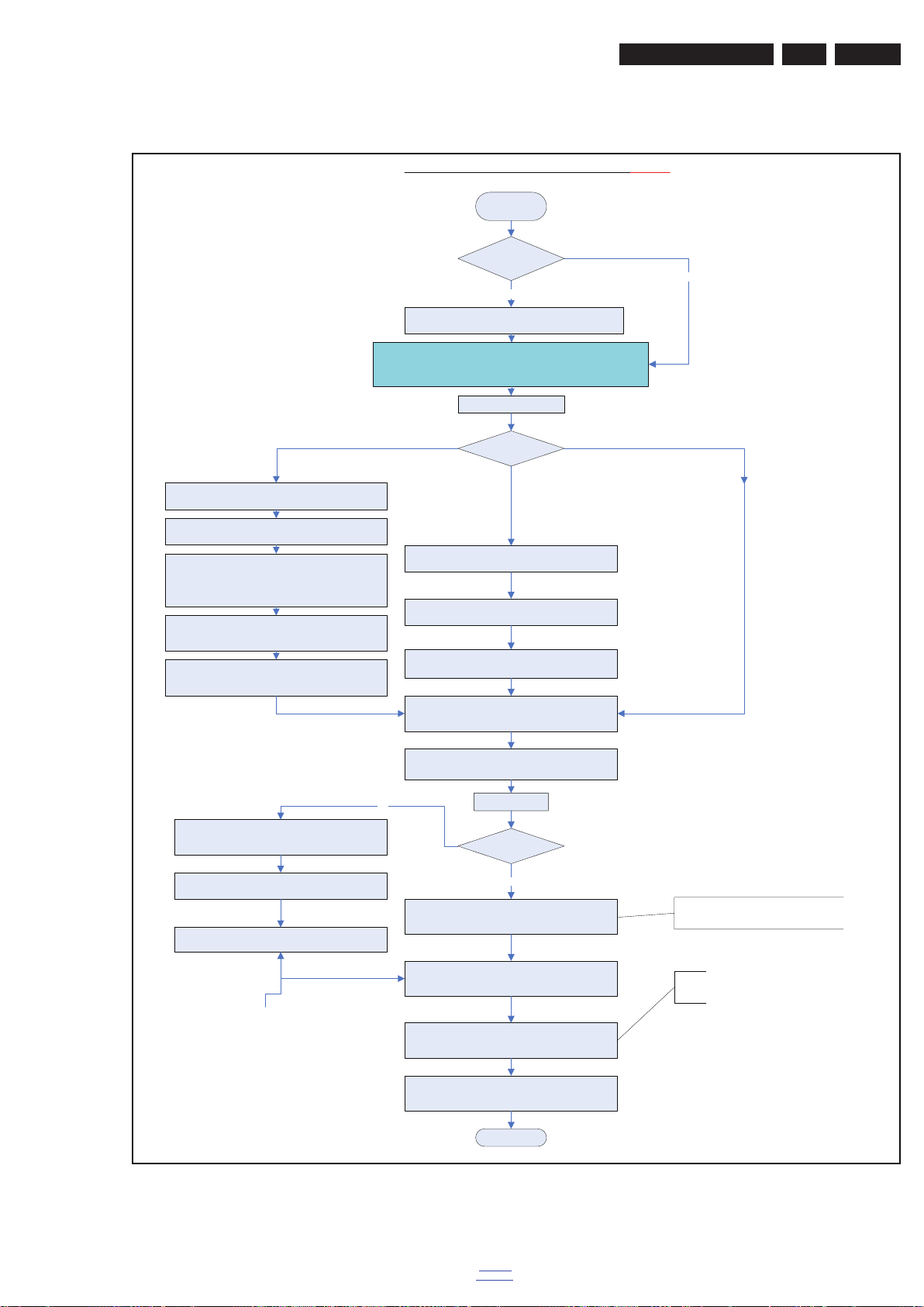
Service Modes, Error Codes, and Fault Finding
H_16771_007a.eps
100402
START
C onn ect the US B sti ck to th e set,
go to SAM and save the current TV settings via “Upload to USB”
Set is stil l operating?
Yes
1.
D isco nnect the WiFi modu le fro m the P CI c onnec tor (only for Q549.x SSB)
2. Replace the SSB by a Service SSB.
3. Place the WiFi module in the PCI connector.
4. Mount the Service SSB in the set.
Set behaviour?
Yes
No
No
Instru ction n ote SSB replacemen t Q543.x, Q548.x, Q549.x, and Q55x.x
Before starting:
- prepare a USB memory stick with the latest software
- download the latest Main Software (Fus) from www.p4c.philips.com
- unzip this file
- create a folder ”upgrades” in the root of a USB stick (size > 50 MB) and
save the autorun.upg file in this "upgrades" folder.
Note: it is possible to rename this file, e.g."Q54x_SW_version.upg"; this in
case there are more than one "autorun.upg" files on the USB stick.
No pic ture displayed
Pic tur e displayed
Set is starting up without software
upgrade menu appearing on screen
Pic tur e displayed
Set is starting up with software
upgrade menu appearing on screen
Due to a possible wrong display option code in the received Service
SSB (NVM), it’s possible that no picture is displayed. Due to this
the download application will not be shown either. This tree enables you
to load the main software step-by-step via the UART logging on the PC
(this for visual feedback).
Start-up the set
1) Start up the TV set, equiped with the Service SSB,
and enable the UART logging on the PC.
2) The TV set will start-up automatically in the
download application if main TV software is not loaded.
3) Plug the prepared USB stick into the TV set. Follow the
instructions in the UART log file, press “Right” cursor key to enter
the list. Navigate to the “autorun.upg” file in the UART logging
printout via the cursor keys on the remote control. When the
correct file is selected, press “Ok”.
4) Press "Down" cursor and “Ok” to start flashing the main
TV software. Printouts like: “L: 1-100%, V: 1-100% and
P: 1-100%” should be visible now in the UART logging.
5) Wait until the message “Operation successful !” is logged in
the UART log and remove all inserted media. Restart the TV set.
1) Plug the USB stick into the TV set and select
the “autorun .upg” file in the displayed browser.
2) Now the main software will be loaded automatically,
supported by a progress bar.
3) Wait until the message “Operation successful !” is displayed
and remove all inserted media. Restart the TV set.
Set the correct “Display code” via “062598 -HOME- xxx” where
“xxx” is the 3 digit display panel code (see sticker on the side
or bottom of the cabinet)
After entering the “Display Option” code, the set is going to
Standby
(= validation of code)
Restart the set
Connect PC via the ComPair interface to Service connector.
Start TV in Jett mode (DVD I + (OSD))
Open ComPair browser Q54x
Program set type number, serial number, and di
splay 12 NC
Program E - DFU if needed.
Go to SAM and reload settings
via “Download from USB” function.
In case of settings reloaded from USB, the set type,
serial number, display 12 NC, are automatically stored
when entering display options.
- Check if correct “display option” code is programmed.
- Verify “option codes” according to sticker inside the set.
- Default settings for “white drive” > see Service Manual.
Q54x.E SSB Board swap – VDS
Updated 22-03-2010
If not already done:
Check latest software on Service website.
Update main and Stand-by software via USB.
Check and perform alignments in SAM according to the
Service Manual. Option codes, colour temperature, etc.
Final check of all menus in CSM.
Special attention for HDMI Keys and Mac address.
Check if E - D F U is present.
End
Attention point for Net TV: If the set type and serial number are not
filled in, the Net TV functionality will not work. It will not be possible
to connect to the internet.
Saved settings
on USB stick?
5.8.13 SSB Replacement
Follow the instructions in the flowchart in case a SSB has to be
exchanged. See figure “SSB replacement flowchart”.
EN 37Q552.2L LA 5.
Figure 5-11 SSB replacement flowchart
back to
div. table
2011-Jul-15
Page 38
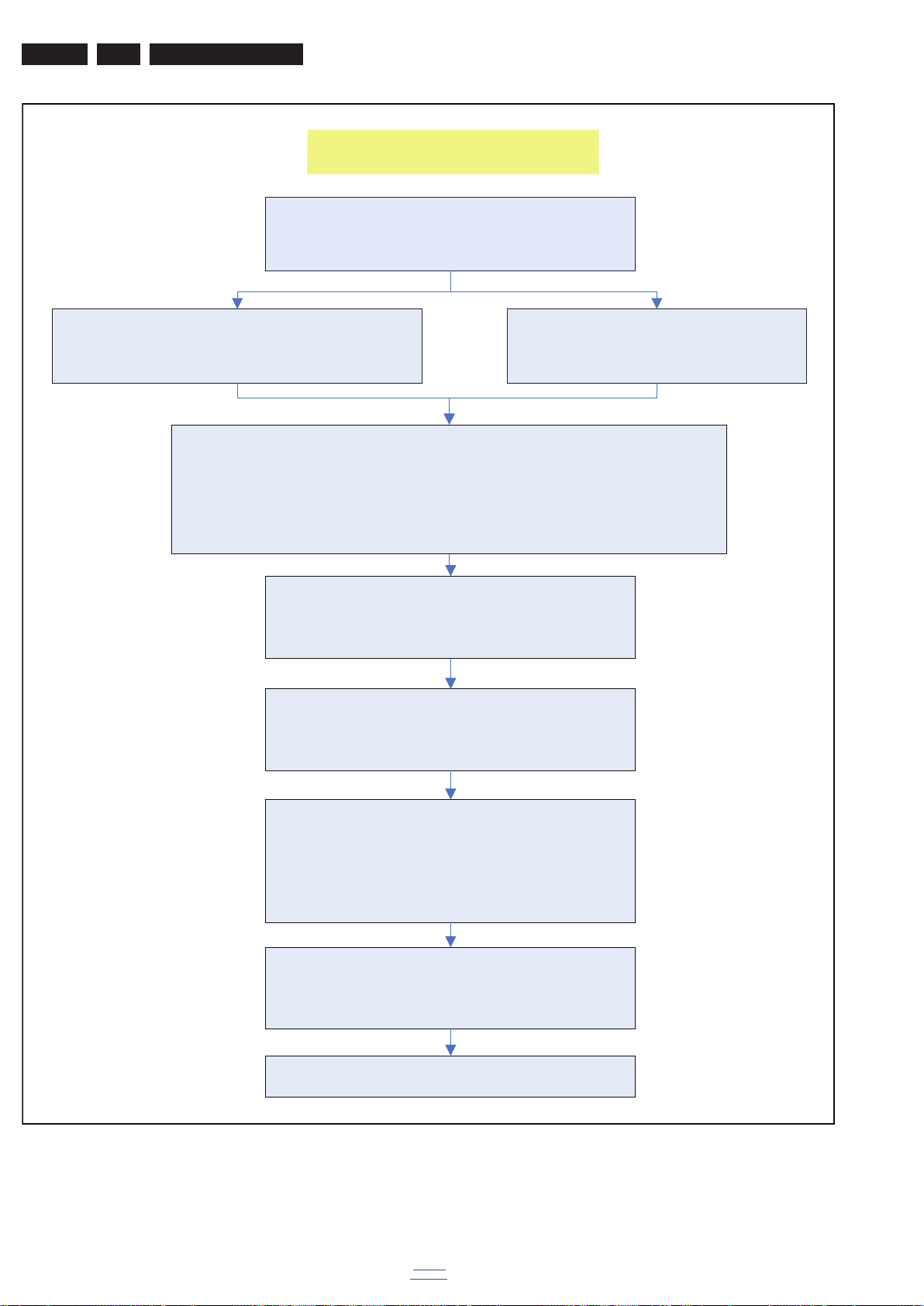
EN 38 Q552.2L LA5.
Service Modes, Error Codes, and Fault Finding
Set is starting up in Factory mode
Set is starting up in Factory m ode?
Noisy picture with bands/lines is visible and the
RED LED is continuous on.
- Press the “volume minus” button on the TVs local keyboard for 5 ~10
- Press the “SOURCE” button for 10 seconds until the “F” disappears
from the screen or the noise on the screen is replaced by “blue mute”
The noise on the screen is replaced
with the blue mute or the “F” is disappeared!
Unplug the mains cord to verify the correct
disabling of the Factory mode.
seconds
An “F” is displayed (and the HDMI 1
input is displayed).
2011-Jul-15
Program display option code
via “062598 MENU”, followed by
the 3 digits code of the display
(this code can be found
on a sticker on - or inside - the set).
After entering “display option” code, the set is
going in stand-by mode (= validation of code)
Restart the set
Figure 5-12 SSB replacement flowchart - Factory mode
back to
div. table
H_16771_007b.eps
100322
Page 39
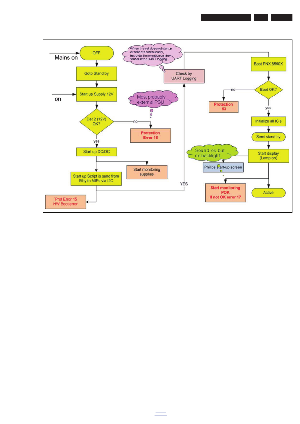
Service Modes, Error Codes, and Fault Finding
18753_211_100811.eps
100811
EN 39Q552.2L LA 5.
5.9 Software Upgrading
Attention!
Software version numbers for 2011 sets are all defined below
number 0.40.x.x. This might confuse servicers who store
software versions for more than one set and/or platform on the
same storage device (USB stick).
Always check the latest software version on the servicer
website in relation to the correct CTN!!!
5.9.1 Introduction
The set software and security keys are stored in a NANDFlash, which is connected to the PNX855xx.
It is possible for the user to upgrade the main software via the
USB port. This allows replacement of a software image in a
stand alone set, without the need of an E-JTAG debugger. A
description on how to upgrade the main software can be found
in the electronic User Manual.
Important: When the NAND-Flash must be replaced, a new
SSB must be ordered, due to the presence of the security keys!
(CI +, MAC address, ...).
Perform the following actions after SSB replacement:
1. Set the correct option codes (see sticker inside the TV).
2. Update the TV software => see the eUM (electronic User
Manual) for instructions.
3. Perform the alignments as described in chapter 6 (section
6.5 Reset of Repaired SSB
4. Check in CSM if the CI + key, MAC address.. are valid.
).
Figure 5-13 SSB start-up
5.9.2 Main Software Upgrade
back to
div. table
For the correct order number of a new SSB, always refer to the
Spare Parts list!
• The “UpgradeAll.upg” file is only used in the factory.
Automatic Software Upgrade
In “normal” conditions, so when there is no major problem with
the TV, the main software and the default software upgrade
application can be upgraded with the “AUTORUN.UPG”
(FUS part of the one-zip file: e.g. 3104 337 05661 _FUS
_Q555X_ x.x.x.x_prod.zip). This can also be done by the
consumers themselves, but they will have to get their software
from the commercial Philips website or via the Software Update
Assistant in the user menu (see eUM). The “autorun.upg” file
must be placed in the root of the USB stick.
How to upgrade:
1. Copy “AUTORUN.UPG” to the root of the USB stick.
2. Insert USB stick in the set while the set is operational. The
set will restart and the upgrading will start automatically. As
soon as the programming is finished, a message is shown
to remove the USB stick and restart the set.
Manual Software Upgrade
In case that the software upgrade application does not start
automatically, it can also be started manually.
How to start the software upgrade application manually:
1. Disconnect the TV from the Mains/AC Power.
2. Press the “OK” button on a Philips TV remote control or a
Philips DVD RC-6 remote control (it is also possible to use
2011-Jul-15
Page 40

EN 40 Q552.2L LA5.
Service Modes, Error Codes, and Fault Finding
a TV remote in “DVD” mode). Keep the “OK” button
pressed while reconnecting the TV to the Mains/AC Power.
3. The software upgrade application will start.
Attention!
In case the download application has been started manually,
the “autorun.upg” will maybe not be recognized.
What to do in this case:
1. Create a directory “UPGRADES” on the USB stick.
2. Rename the “autorun.upg” to something else, e.g. to
“software.upg”. Do not use long or complicated names,
keep it simple. Make sure that “AUTORUN.UPG” is no
longer present in the root of the USB stick.
3. Copy the renamed “upg” file into this directory.
4. Insert USB stick into the TV.
5. The renamed “upg” file will be visible and selectable in the
upgrade application.
Back-up Software Upgrade Application
If the default software upgrade application does not start (could
be due to a corrupted boot sector) via the above described
method, try activating the “back-up software upgrade
application”.
How to start the “back-up software upgrade application”
manually:
1. Disconnect the TV from the Mains/AC Power.
2. Press the “CURSOR DOWN”-button on a Philips TV
remote control while reconnecting the TV to the Mains/AC
Power.
3. The back-up software upgrade application will start.
5.9.3 Stand-by Software Upgrade via USB
In this chassis it is possible to upgrade the Stand-by software
via a USB stick. The method is similar to upgrading the main
software via USB.
Use the following steps:
1. Create a directory “UPGRADES” on the USB stick.
2. Copy the Stand-by software (part of the one-zip file, e.g.
StandbyFactory_88.0.0.0.upg) into this directory.
3. Insert the USB stick into the TV.
4. Start the download application manually (see section “
Manual Software Upgrade”.
5. Select the appropriate file and press the “OK” button to
upgrade.
5.9.4 Content and Usage of the One-Zip Software File
Below the content of the One-Zip file is explained, and
instructions on how and when to use it.
• AmbiCpld_Q55XX_x.x.x.x_prod.zip. Contains the
program instruction and software content, needed to
upgrade the ambilight CPLD on the TV550 platform.
• BalanceFPGA_Q555X_x.x.x.x_prod.zip. Contains the
BalanceFPGA software in “upg” format.
• FUS_Q555X_x.x.x.x_prod.zip. Contains the
“autorun.upg” which is needed to upgrade the TV main
software and the software download application.
• PNX5130UPG_Q555X_x.x.x.x_prod.zip. Contains the
PNX5130 software in “upg” format.
• StandbySW_Q555X_x.x.x.x_prod.zip. Contains the
StandbyFactory software in “upg” format.
• ProcessNVM_Q55XX_x.x.x.x_prod.zip. Default NVM
content. Must be programmed via ComPair or can be
loaded via USB, be aware that all alignments stored in
NVM are overwritten here.
5.9.5 UART logging 2K10 (see section “5.8 Fault Finding and
Repair Tips, 5.8.7 Logging)
2011-Jul-15
back to
div. table
Page 41
6. Alignments
Alignments
EN 41Q552.2L LA 6.
Index of this chapter:
6.1 General Alignment Conditions
6.2 Hardware Alignments
6.3 Software Alignments
6.4 Option Settings
6.5 Reset of Repaired SSB
6.6 Total Overview SAM modes
6.1 General Alignment Conditions
Perform all electrical adjustments under the following
conditions:
• Power supply voltage (depends on region):
– AP-NTSC: 120 VAC or 230 V
– AP-PAL-multi: 120 - 230 V
– EU: 230 V
/ 50 Hz (r 10%).
AC
– LATAM-NTSC: 120 - 230 V
– US: 120 V
/ 60 Hz (r 10%).
AC
/ 50 Hz (r 10%).
AC
/ 50 Hz (r 10%).
AC
/ 50 Hz (r 10%).
AC
• Connect the set to the mains via an isolation transformer
with low internal resistance.
• Allow the set to warm up for approximately 15 minutes.
• Measure voltages and waveforms in relation to correct
ground (e.g. measure audio signals in relation to
AUDIO_GND).
Caution: It is not allowed to use heat sinks as ground.
• Test probe: Ri > 10 M:, Ci < 20 pF.
• Use an isolated trimmer/screwdriver to perform
alignments.
6.1.1 Alignment Sequence
• First, set the correct options:
– In SAM, select “Option numbers”.
– Fill in the option settings for “Group 1” and “Group 2”
according to the set sticker (see also paragraph 6.4
Option Settings).
– Press OK on the remote control before the cursor is
moved to the left.
– In submenu “Option numbers” select “Store” and press
OK on the RC.
•OR:
– In main menu, select “Store” again and press OK on
the RC.
– Switch the set to Stand-by.
• Warming up (>15 minutes).
6.2 Hardware Alignments
Not applicable.
6.3 Software Alignments
Put the set in SAM mode (see Chapter 5. Service Modes, Error
Codes, and Fault Finding). The SAM menu will now appear on
the screen. Select ALIGNMENTS and go to one of the sub
menus. The alignments are explained below.
The following items can be aligned:
• White point
• Ambilight.
To store the data:
• Press OK on the RC before the cursor is moved to the
left
• In main menu select “Store” and press OK on the RC
• Switch the set to stand-by mode.
For the next alignments, supply the following test signals via a
video generator to the RF input:
• EU/AP-PAL models: a PAL B/G TV-signal with a signal
strength of at least 1 mV and a frequency of 475.25 MHz
• US/AP-NTSC models: an NTSC M/N TV-signal with a
signal strength of at least 1 mV and a frequency of 61.25
MHz (channel 3).
• LATAM models: an NTSC M TV-signal with a signal
strength of at least 1 mV and a frequency of 61.25 MHz
(channel 3).
6.3.1 White Point
• Choose “TV menu”, “Setup”, “More TV Settings” and then
“Picture” and set picture settings as follows:
Picture Setting
Contrast 100
Brightness 50
Colour 0
Light Sensor Off
Picture format Unscaled
• In menu “Picture”, choose “Pixel Plus HD” and set picture
settings as follows:
Picture Setting
Dynamic Contrast Off
Dynamic Backlight Off
Colour Enhancement Off
Gamma 0
• Go to the SAM and select “Alignments”-> “White point”.
White point alignment LCD screens:
• Use a 100% white screen (format: 720p50) to the HDMI
input and set the following values:
– “Color temperature”: “Cool”.
– All “White point” values to: “127”.
In case you have a color analyzer:
• Measure, in a dark environment, with a calibrated
contactless color analyzer (Minolta CA-210 or Minolta CS-
200) in the centre of the screen and note the x, y value.
• Change the pattern to 90% white screen. If a Quantum
Data generator is used, select the “GreyAll” test pattern at
level = 230.
• Adjust the correct x, y coordinates (while holding one of the
White point registers R, G or B on 127) by means of
decreasing the value of one or two other white points to the
correct x, y coordinates (see Table 6-1 White D alignment
values - LED - Minolta CA-210, or 6-2 White D alignment
values - LED - Minolta CS-200). Tolerance: dx: r 0.002, dy:
r 0.002.
• Repeat this step for the other color temperatures that need
to be aligned.
• When finished press OK on the RC and then press STORE
(in the SAM root menu) to store the aligned values to the
NVM.
• Restore the initial picture settings after the alignments.
Table 6-1 White D alignment values - LED - Minolta CA-210
Value Cool (9420K) Normal (8120K) Warm (6080K)
x 0.282 0.292 0.320
y 0.298 0.311 0.345
Table 6-2 White D alignment values - LED - Minolta CS-200
Value Cool (11000K) Normal (9000K) Warm (6500K)
x 0.276 0.287 0.313
y 0.282 0.296 0.329
back to
div. table
2011-Jul-15
Page 42
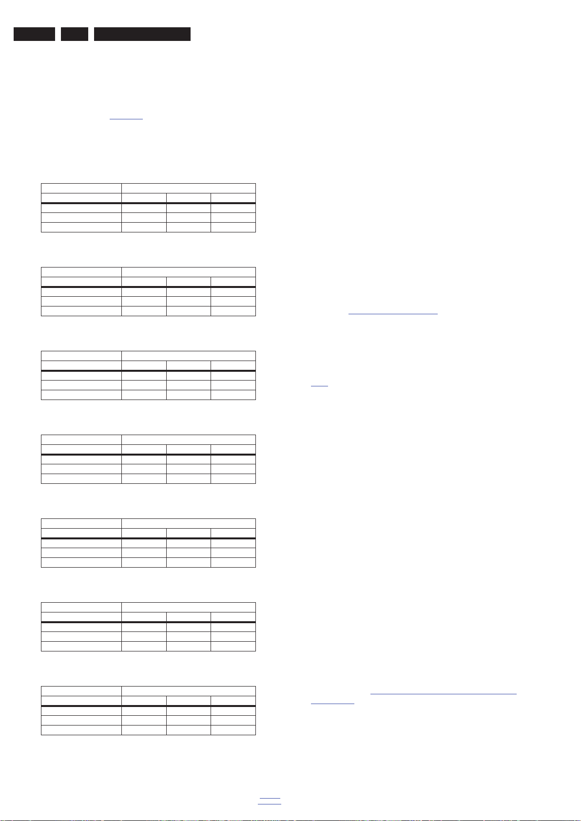
EN 42 Q552.2L LA6.
Alignments
If you do not have a color analyzer, you can use the default
values. This is the next best solution. The default values are
average values coming from production.
• Select a COLOUR TEMPERATURE (e.g. COOL,
NORMAL, or WARM).
• Set the RED, GREEN and BLUE default values according
to the values in Table 6-3
.
• When finished press OK on the RC, then press STORE (in
the SAM root menu) to store the aligned values to the NVM.
• Restore the initial picture settings after the alignments.
Table 6-3 White tone default setting 32" sets (Blockbuster)
White Tone e.g. 32PFL6606/xx
Colour Temp R G B
Normal t.b.d. t.b.d. t.b.d.
Cool t.b.d. t.b.d. t.b.d.
Warm t.b.d. t.b.d. t.b.d.
Table 6-4 White tone default setting 40" sets (Blockbuster)
White Tone e.g. 40PFL6606/xx
Colour Temp R G B
Normal 117 127 95
Cool 113 127 111
Warm 126 125 60
Table 6-5 White tone default setting 32" sets (Emmy)
6.4 Option Settings
6.4.1 Introduction
The microprocessor communicates with a large number of I
ICs in the set. To ensure good communication and to make
digital diagnosis possible, the microprocessor has to know
which ICs to address. The presence / absence of these
PNX51XX ICs (back-end advanced video picture improvement
IC which offers motion estimation and compensation features
(commercially called HDNM) plus integrated Ambilight control)
is made known by the option codes.
Notes:
• After changing the option(s), save them by pressing the OK
button on the RC before the cursor is moved to the left,
select STORE in the SAM root menu and press OK on the
RC.
• The new option setting is only active after the TV is
switched “off” / “stand-by” and “on” again with the mains
switch (the NVM is then read again).
6.4.2 Dealer Options
For dealer options, in SAM select “Dealer options”.
See Table 6-11 SAM mode overview
6.4.3 (Service) Options
.
2
C
White Tone e.g. 32PFL7606/xx
Colour Temp R G B
Normal 112 127 85
Cool 106 127 100
Warm 125 126 53
Table 6-6 White tone default setting 40" sets (Emmy)
White Tone e.g. 40PFL7606/xx
Colour Temp R G B
Normal 115 127 84
Cool 111 127 99
Warm 125 127 49
Table 6-7 White tone default setting 46" sets (Emmy)
White Tone e.g. 46PFL7606/xx
Colour Temp R G B
Normal 124 127 98
Cool 120 127 121
Warm 127 121 58
Table 6-8 White tone default setting 42" sets (Sundance)
White Tone e.g. 42PFL8606/xx
Colour Temp R G B
Normal 125 125 127
Cool 106 108 127
Warm 127 110 79
Table 6-9 White tone default setting 47" sets (Sundance)
White Tone e.g. 47PFL8606/xx
Colour Temp R G B
Normal t.b.d. t.b.d. t.b.d.
Cool t.b.d. t.b.d. t.b.d.
Warm t.b.d. t.b.d. t.b.d.
From 2011 onwards, it is not longer possible to change
individual option settings in SAM. Options can only be changed
all at once by using the option codes as described in section
6.4.4
.
6.4.4 Opt. No. (Option numbers)
Select this sub menu to set all options at once (expressed in
two long strings of numbers).
An option number (or “option byte”) represents a number of
different options. When you change these numbers directly,
you can set all options very quickly. All options are controlled
via eight option numbers.
When the NVM is replaced, all options will require resetting. To
be certain that the factory settings are reproduced exactly, you
must set both option number lines. You can find the correct
option numbers on a sticker inside the TV set.
Example: The options sticker gives the following option
numbers:
• 08192 00133 01387 45160
• 12232 04256 00164 00000
The first line (group 1) indicates hardware options 1 to 4, the
second line (group 2) indicate software options 5 to 8.
Every 5-digit number represents 16 bits (so the maximum value
will be 65536 if all options are set).
When all the correct options are set, the sum of the decimal
values of each Option Byte (OB) will give the option number.
Diversity
Not all sets with the same Commercial Type Number (CTN)
necessarily have the same option code!
Use of Alternative BOM => an alternative BOM number usually
indicates the use of an alternative display or power supply. This
results in another display code thus in another Option code.
Refer to Chapter 2. Technical Specifications, Diversity, and
Connections.
6.4.5 Option Code Overview
Refer to the sticker in the set for the correct option codes.
Important: after having edited the option numbers as
described above, you must press OK on the remote control
before the cursor is moved to the left!
2011-Jul-15
back to
div. table
Page 43
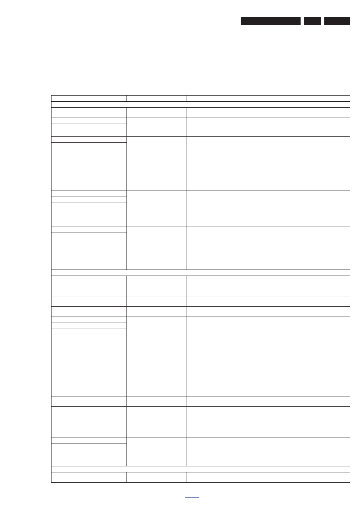
Alignments
EN 43Q552.2L LA 6.
6.4.6 Option Bit Overview
For test purposes, please find below an overview of the Option
Codes on bit level. With a bin/dec converter, you can calculate
the Option Code.
Table 6-10 Option codes at bit level (Option 1 - Option 8)
Option & Bit Dec. Value Option Name
Option 1 (prescribed value 327761))
Bit 15 (MSB) 32768 Video Store Streaming
Bit 14 16384 Multi App
Bit 13 8192
Bit 12 4096 Perfect Pixel
Bit 11 2048
Bit 10 1024 Tuner Type
Bit 9 512
Bit 8 256
Bit 7 128 PQ Profiles
Bit 6 64
Bit 5 32
Bit 4 16 DNM
Bit 3 8
Bit 2 4 MOP AL
Bit 1 2 AL Optical Syst
Bit 0 (LSB) 1
1)
Option 2 (prescribed value 00001
Bit 15 (MSB) 32768 AL Shop Mode
Bit 14 16384 AL settings storage location
Bit 13 8192 Wall Adaptive AL
Bit 12 4096 Sunset
Bit 11 2048 Ambient Light
Bit 10 1024
Bit 9 512
Bit 8 256
Bit 7 128 FPGA3Dact/1Ddimm
Bit 6 64 AL Select
Bit 5 32 3D Passive
Bit 4 16 Smart Bit Enhancement (SBE)
Bit 3 8 Super Resolution
Bit 2 4 Light Sensor LUT
Bit 1 2
Bit 0 (LSB) 1 Light Sensor
Option 3 (prescribed value 154211))
Bit 15 (MSB) 32768 Side IO
)
Prescribed Value
1)
1
1)
00
1)
00
1)
000
1)
000
1)
01
1)
0
1)
00
1)
0
1)
0
1)
0
1)
0
1)
0000
1)
0
1)
0
1)
0
1)
0
1)
0
1)
00
1)
1
1)
0
Caution
When manipulating option codes, know what you’re doing.
Wrong option codes could damage the set.
Prescribed option codes below are an example, not valid for all
sets and are subject to modification.
The correct option codes are always present on a sticker inside
the set!
1)
Description
0 = OFF
1 = ON
00 = none
01 = multi app (Multiview BASIC)
10 = AVPIP + multi app (Multiview ENHANCED)
11 = future use
00 = Pixel Plus HD
01 = Pixel Precise HD
10 = Perfect Pixel HD
11 = future use
000 = TH2603 (Europe/AP)
001 = FA2307 (Brazil)
010 = VA1E1ED2411
011 = future use
100 = future use
101 = future use
110 = future use
111 = future use
000 = profile 0
001 = profile 1
010 = profile 2
011 = profile 3
100 = profile 4
101 = profile 5
110 = profile 6
111 = profile 7
00 = Perfect Natural Motion
01 = HD Natural Motion
10 = future use
11 = future use
CPLD, not used in 2011
00 = 140 nit
01 = 200 nit
10 = future use
11 = future use
0 = boost mode in shop is OFF
1 = boost mode in shop is ON
0 = stored in AL modules
1 = stored in SSB
0 = OFF
1 = ON
0 = OFF
1 = ON
0000 = none
0001 = 2-sided (3/3)
0010 = 2-sided (4/4)
0011 = 2-sided (5/5)
0100 = 2-sided (6/6)
0101 = 2-sided (7/7)
0110 = 3-sided (5/5/5)
0111 = 3-sided (6/6/6)
1000 = 3-sided (3/6/3)
1001 = 3-sided (6/9/6)
1010 = 2-sided (8/8)
1011 = 3-sided (4/4/4)
1100 = 2-sided (1/1)
1101 = 2-sided (2/2)
1110 = future use
1111 = future use
0 = OFF
1 = ON
0 = AL2k10
1 = AL2k11
0 = 2D
1 = 3D passive
0 = off
1 = on (200 Hz board present)
0 = Super Resolution SD
1 = Super Resolution HD
00 = Lut 0
01 = Lut 1
10 = Lut 2
11 = Lut 3
0 = OFF
1 = ON
0 = not present
1 = present
back to
div. table
2011-Jul-15
Page 44
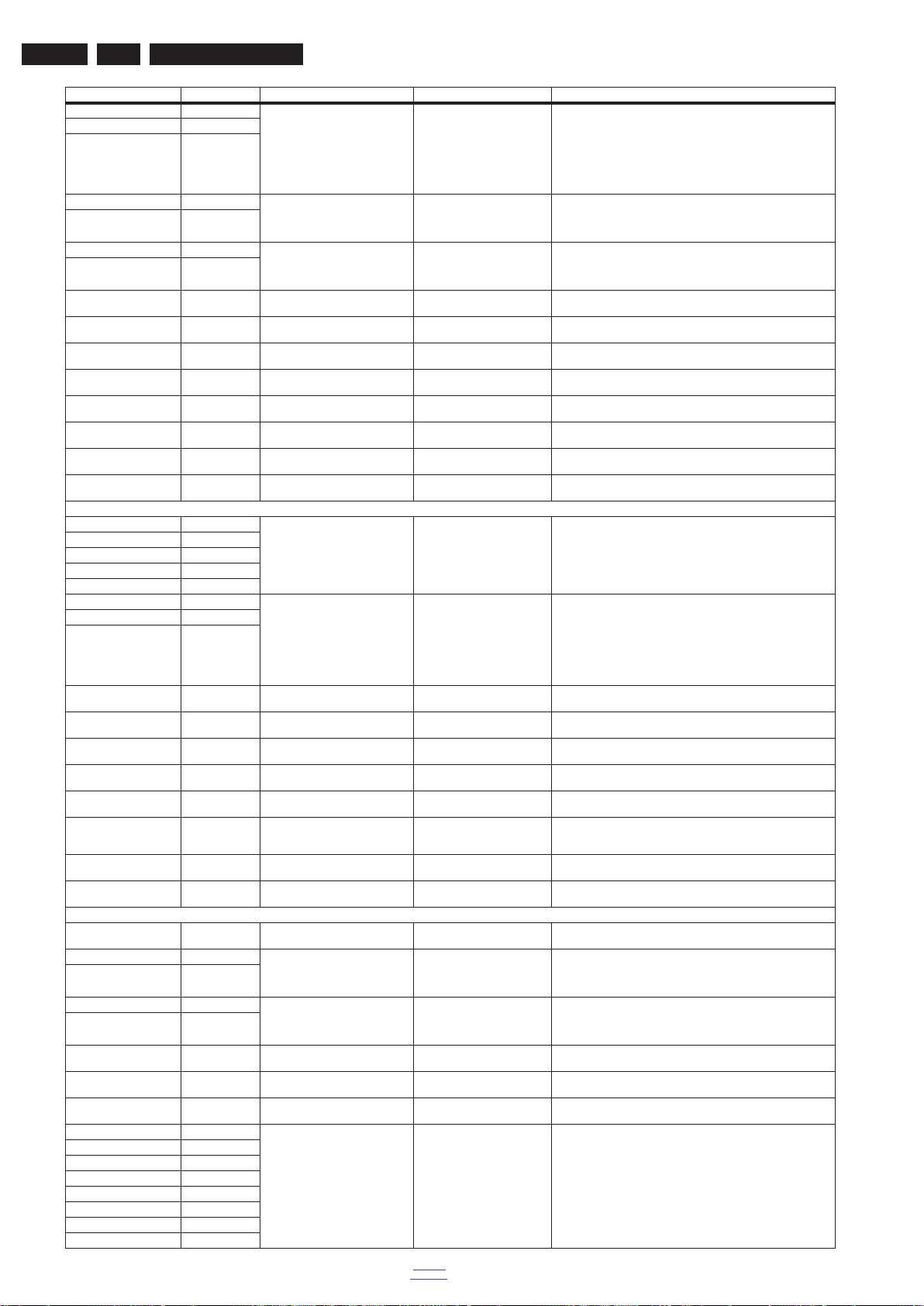
EN 44 Q552.2L LA6.
Alignments
Option & Bit Dec. Value Option Name
Bit 14 16384 AV3
Bit 13 8192
Bit 12 4096
Bit 11 2048 AV2
Bit 10 1024
Bit 9 512 AV1
Bit 8 256
Bit 7 128 3D Prepared
Bit 6 64 Sound in Stand
Bit 5 32 Headphone
Bit 4 16 Seamless System
Bit 3 8 ViewPort 21_9/PQL
Bit 2 4 HDMI Side
Bit 1 2 HDMI 3
Bit 0 (LSB) 1 HDMI 2
Option 4 (prescribed value 022351))
Bit 15 (MSB) 32768 Cabinet
Bit 14 16384
Bit 13 8192
Bit 12 4096
Bit 11 2048
Bit 10 1024 Region
Bit 9 512
Bit 8 256
Bit 7 128 Display MSB
Bit 6 64 S Video
Bit 5 32 Video Store SD Card
Bit 4 16 Internet SW Upgrade
Bit 3 8 Online Service
Bit 2 4 WiFi
Bit 1 2 DLNA
Bit 0 (LSB) 1 Ethernet
1)
Option 5 (prescribed value 43847
)
Bit 15 (MSB) 32768 8 Days EPG
Bit 14 16384 DVBC Installation
Bit 13 8192
Bit 12 4096 DVBT Installation
Bit 11 2048
Bit 10 1024 DVB-S
Bit 9 512 DVB-C
Bit 8 256 DVB
Bit 7 128 Display Type
Bit 6 64
Bit 5 32
Bit 4 16
Bit 3 8
Bit 2 4
Bit 1 2
Bit 0 (LSB) 1
Prescribed Value
1)
011
1)
11
1)
00
1)
0
1)
0
1)
1
1)
1
1)
1
1)
1
1)
0
1)
1
1)
00001
1)
000
1)
1
1)
0
1)
1
1)
1
1)
1
1)
0
1)
1
1)
1
1)
1
1)
01
1)
01
1)
0
1)
1
1)
1
1)
01000111
1)
Description
000 = none
001 = CVBS
010 = YPbPr
011 = YPbPr/LR
100 = YPbPr/HV/LR
101 = CVBS/LR
110 = CVBS/Yc/LR
111 = future use
00 = Scart/CVBS/RGB/LR
01 = CVBS/LR
10 = YPbPr/LR
11 = none
00 = Scart/CVBS/RGB/LR
01 = CVBS/YC/YPbPr/HV/LR
10 = CVBS/YC/YPbPr/LR
11 = YPbPr/LR
0 = not prepared
1 = prepared
0 = Sound in Cabinet
1 = Sound in Stand
0 = OFF
1 = ON
0 = OFF
1 = ON
0 = OFF
1 = ON
0 = OFF
1 = ON
0 = OFF
1 = ON
0 = OFF
1 = ON
Cabinet type
(no detailed info available)
000 = Europe (/02, /05 & /12)
001 = AP PAL multi
010 = AP NTSC
011 = Russian (/60)
100 = Latam (/78 & /77)
101 = Australia
110 = China (/93)
111 = future use
0 = display option =< 255
1 = display option > 255
0 = OFF
1 = ON
0 = OFF
1 = ON
0 = OFF
1 = ON (automatic software upgradable via internet)
0 = OFF
1 = ON (connection to internet provider Philips)
0 = OFF
1 = ON (wireless connection to ethernet; no link with “Ethernet option” bit “0”)
0 = OFF
1 = PC link
0 = OFF
1 = Ethernet vonnector and HW present
0 = OFF
1 = ON (country dependent)
00 = OFF
01 = Country dependent
10 = ON
11 = future use
00 = OFF
01 = Country dependent
10 = ON
11 = future use
0 = OFF
1 = ON (ATSC/DVB should be ON)
0 = OFF
1 = ON (ATSC/DVB should be ON)
0 = analogue only
1 = DVBT (and C/S depending DVBC/S option)
Display Type (ex.: 327)
2011-Jul-15
back to
div. table
Page 45
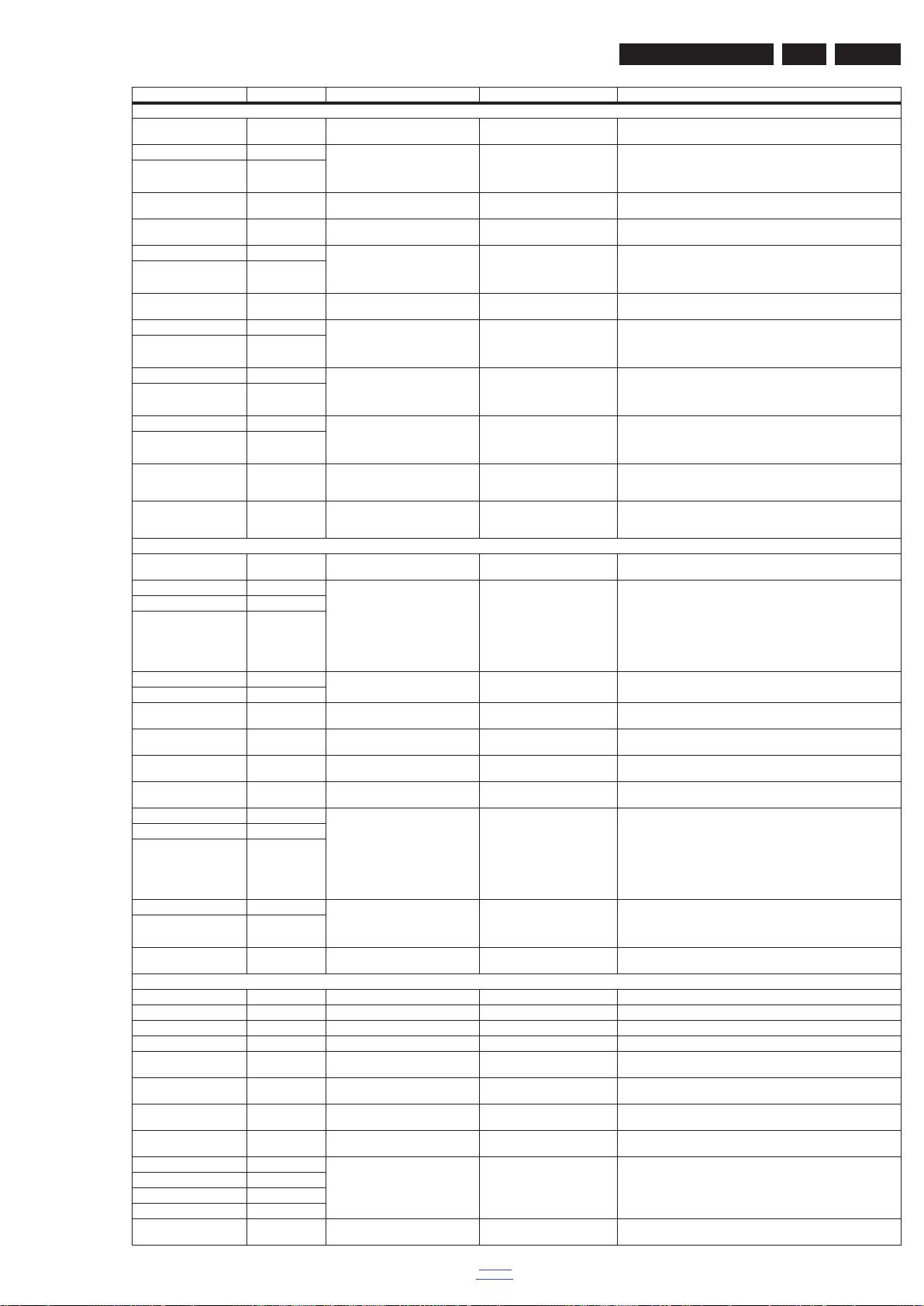
Alignments
EN 45Q552.2L LA 6.
Option & Bit Dec. Value Option Name
Option 6 (prescribed value 366151))
Bit 15 (MSB) 32768 E-sticker
Bit 14 16384 Hotel Mode
Bit 13 8192
Bit 12 4096 Virgin
Bit 11 2048 USB Time Shift
Bit 10 1024 Auto Store Mode
Bit 9 512
Bit 8 256 PVR
Bit 7 128 Ginga
Bit 6 64
Bit 5 32 MHP
Bit 4 16
Bit 3 8 Over the Air Download
Bit 2 4
Bit 1 2 DVBC light
Bit 0 (LSB) 1 DVBT light
Option 7 (prescribed value 330241))
Bit 15 (MSB) 32768 Visual Identity
Bit 14 16384 Red LED Config LUT
Bit 13 8192
Bit 12 4096
Bit 11 2048 Board Identifier
Bit 10 1024
Bit 9 512 Manet
Bit 8 256 Auto Power Down
Bit 7 128 Light Guide
Bit 6 64 E-box
Bit 5 32 Temp LUT
Bit 4 16
Bit 3 8
Bit 2 4 Temp Sensor
Bit 1 2
Bit 0 (LSB) 1 FAN
Option 8 (prescribed value 00012
1)
)
Bit 15 (MSB) 32768 Test 8
Bit 14 16384 Test 7
Bit 13 8192 Test 6
Bit 12 4096 Test 5
Bit 11 2048 Test 4 (Trick Mode)
Bit 10 1024 Test 3 (XRay)
Bit 9 512 Test 2 (DBV-T light)
Bit 8 256 Test 1 (Monitor out)
Bit 7 128 not used
Bit 6 64
Bit 5 32
Bit 4 16
Bit 3 8 WM DRM10
Prescribed Value
1)
1
1)
00
1)
0
1)
1
1)
11
1)
1
1)
00
1)
00
1)
01
1)
1
1)
1
1)
1
1)
000
1)
00
1)
0
1)
1
1)
0
1)
0
1)
000
1)
00
1)
0
1)
0
1)
0
1)
0
1)
0
1)
0
1)
0
1)
0
1)
0
1)
0000
1)
1
1)
Description
0 = OFF
1 = ON
00 = OFF
01 = 1V1
10 = 1V2
11 = future use
0 = ON
1 = OFF
0 = OFF
1 = ON
00 = none
01 = PDC_VPS
10 = TXT page
11 = PDC_VPS_TXT
0 = OFF
1 = ON
00 = OFF
01 = Country dependent
10 = ON
11 = future use
00 = OFF
01 = Country dependent
10 = ON
11 = future use
00 = OFF
01 = Country dependent
10 = ON
11 = future use
0 = OFF
1 = ON (when DVBC Installation is OFF or when ON but selected
country is OFF, this option is used)
0 = OFF
1 = ON (when DVBT Installation is OFF or Country depend to a
country is OFF, this option is used)
0 = User Interface 2k10
1 = User Interface 2k11
000 = LED config LUT 0
001 = LED config LUT 1
010 = LED config LUT 2
011 = LED config LUT 3
100 = LED config LUT 4
101 = LED config LUT 5
110 = LED config LUT 6
111 = LED config LUT 7
not used, should always be “00”
0 = all sets except Manet
1= Manet
0 = OFF
1 = ON
0 = OFF
1 = ON
0 = integrated set
1 = e-box/monitor
000 = temp lut 0
001 = temp lut 1
010 = temp lut 2
011 = temp lut 3
100 = future use
101 = future use
110 = future use
111 = future use
00 = no temp sensor
01 = temp sensor in display
10 = temp sensor on addition al board
11 = temp sensor in AL module
0 = no fan
1 = fan(s) present)
-
-
-
-
0 = OFF
1 = ON
0 = OFF
1 = ON
0 = OFF
1 = ON
0 = OFF
1 = ON
-
0 = OFF
1 = ON
back to
div. table
2011-Jul-15
Page 46
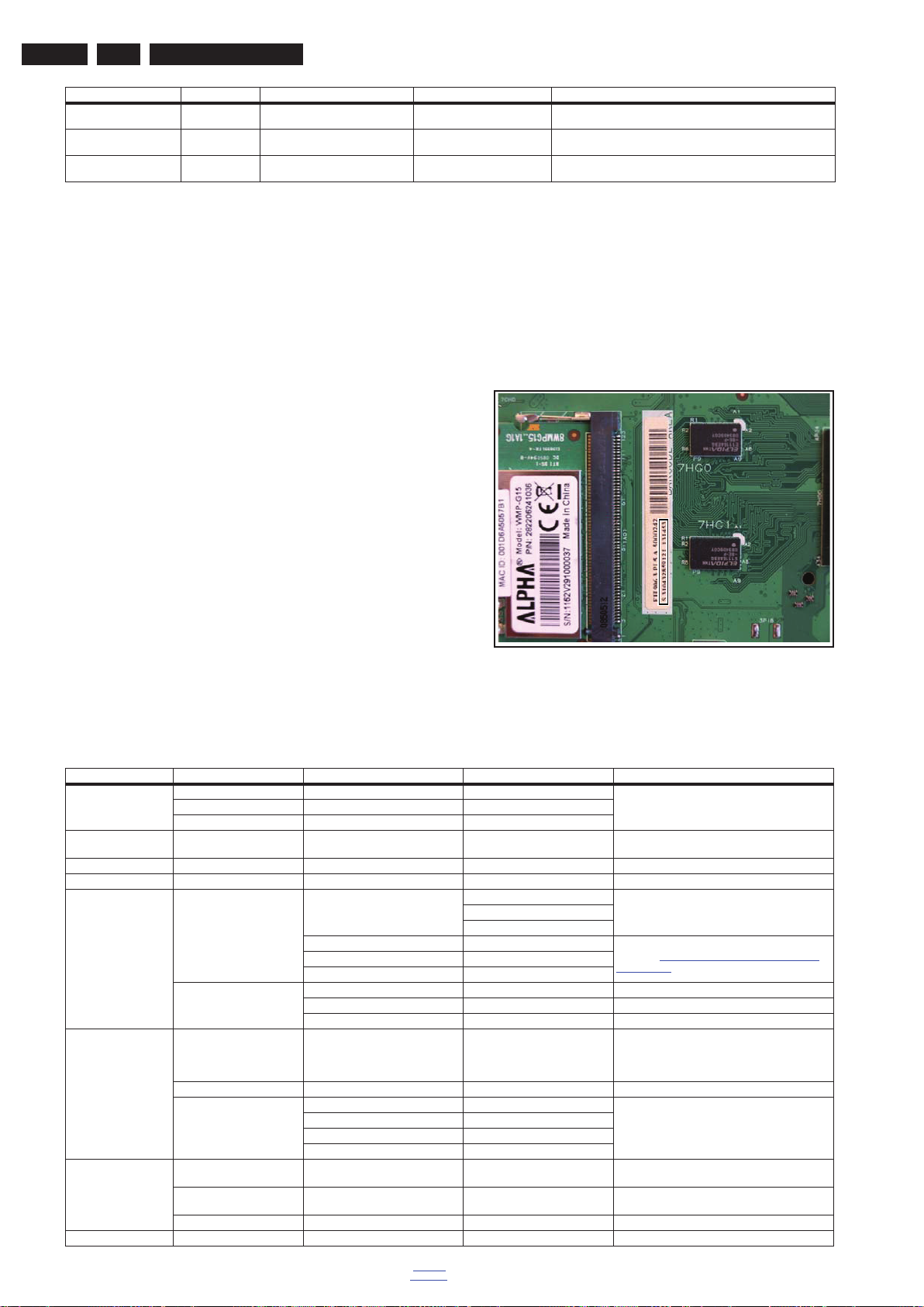
EN 46 Q552.2L LA6.
Alignments
Option & Bit Dec. Value Option Name
Bit 2 4 HBBTV
Bit 1 2 DVB-T2 Installation
Bit 0 (LSB) 1 DVB-T2
Note
1). Example
6.5 Reset of Repaired SSB
A very important issue towards a repaired SSB from a Service
repair shop (SSB repair on component level) implies the reset
of the NVM on the SSB.
A repaired SSB in Service should get the service Set type
“00PF0000000000” and Production code “00000000000000”.
Also the virgin bit is to be set. To set all this, you can use the
ComPair tool or use the “NVM editor” and “Dealer options”
items in SAM (do not forget to “store”).
After a repaired SSB has been mounted in the set (set repair
on board level), the type number (CTN) and production code of
the TV has to be set according to the type plate of the set. For
this, you can use the NVM editor in SAM. This action also
ensures the correct functioning of the “Net TV” feature and
access to the Net TV portals. The loading of the CTN and
production code can also be done via ComPair (Model number
programming).
Prescribed Value
1)
1
1)
0
1)
0
1)
In case of a display replacement, reset the “Operation hours
display” to “0”, or to the operation hours of the replacement
display.
6.5.1 SSB identification
Whenever ordering a new SSB, it should be noted that the
correct ordering number (12nc) of a SSB is located on a sticker
on the SSB. The format is <12nc SSB><serial number>. The
ordering number of a “Service” SSB is the same as the ordering
number of an initial “factory” SSB.
Description
0 = OFF
1 = ON
0 = OFF
1 = ON
0 = OFF
1 = ON
After a SSB repair, the original channel map can be restored,
provided that the original channel map was stored on a USB
stick before repair was commenced and that basic functionality
of the TV, needed for this procedure, was not hampered as a
result of the defect. The procedure of “channel map cloning” is
clearly described in the (electronic) user manual.
6.6 Total Overview SAM modes
Table 6-11 SAM mode overview
Main Menu Sub-menu 1 Sub-menu 2 Sub-menu 3 Description
Hardware Info A. SW version e.g. “Q5551_0.9.1.0 Display TV & Stand-by SW version and CTN serial
B. Stand-by processor version e.g. “STDBY_83.84.0.0”
C. Production code e.g. “see type plate”
Operation hours Displays the accumulated total of operation hours.TV
Errors Displayed the most recent errors
Reset error buffer Clears all content in the error buffer
Alignment White point Colour temperature Normal 3 different modes of colour temperature can be
White point red LCD White Point Alignment. For values,
White point green
White point blue
Ambilight Select module
Brightness
Select matrix
Dealer options Virgin mode Off/On Select Virgin mode On/Off. TV starts up / does not
E-sticker Off/On Select E-sticker On/Off (USP’s on-screen)
Auto store mode None
PDC/VPS
TXT page
PDC/VPS/TXT
Option numbers Group 1 e.g. “00008.00001.15421.02239” The first line (group 1) indicates hardware options 1
Group 2 e.g. “44816.34311.33024.00000” The second line (group 2) indicates software options
Store Store after changing
Initialise NVM N.A.
Warn
Cool
18310_221_090318.eps
number
switched “on/off” & every 0.5 hours is increase one
selected
see Table 6-3 White tone default setting 32" sets
(Blockbuster)
start up (once) with a language selection menu after
the mains switch is turned “on” for the first time (virgin
mode)
to 4
5 to 8
090319
2011-Jul-15
back to
div. table
Page 47
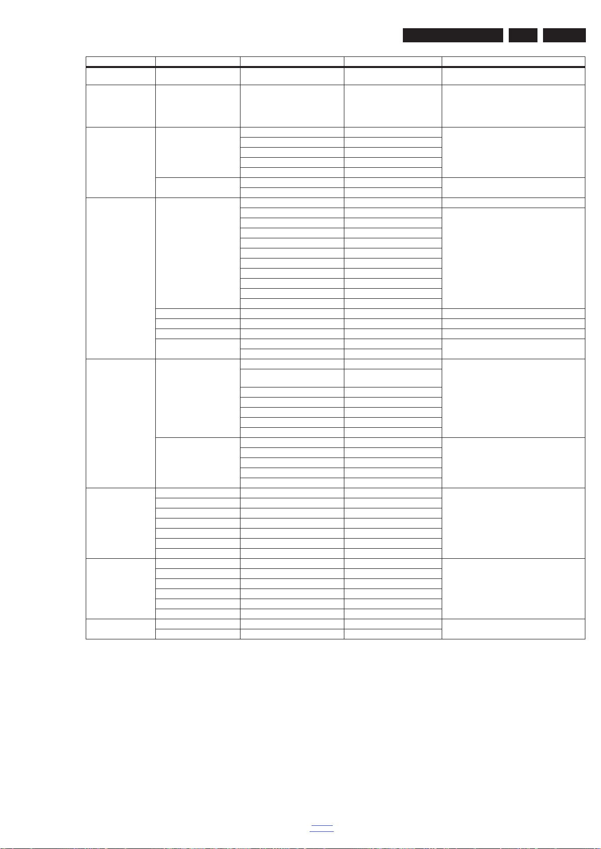
Alignments
Main Menu Sub-menu 1 Sub-menu 2 Sub-menu 3 Description
Store Select Store in the SAM root menu after making any
Operation hours display 0003 In case the display must be swapped for repair, you
Software maintenance Software events Display Display information is for development purposes
Hardware events Display Display information is for development purposes
Test setting Digital info Current frequency: 538
Install start frequency 000 Install start frequency from “0” MHz
Install end frequency 999 Install end frequency as “999” MHz
Default install frequency
Installation Digital only Select Digital only or Digital + Analogue before
Development file
versions
Upload to USB Channel list To upload several settings from the TV to an USB
Download from USB Channel list To download several settings from the USB stick to
NVM editor Type number see type plate NVM editor; re key-in type number and production
Development 1 file version Display parameters DISPT5.0.9.29 Display information is for development purposes
Development 2 file version 12NC one zip software Display information is for development purposes
Personal settings
Option codes
Alignments
Identification data
History list
All (options included)
Personal settings
Option codes
Alignments
Identification data
All (options included)
AG code see type plate
Clear
Test reboot
Test cold reboot
Test application crash
Clear
QAM modulation: 64-qam Display information is for development purposes
Symbol rate:
Original network ID: 12871
Network ID: 12871
Transport stream ID: 2
Service ID: 3
Hierarchical modulation: 0
Selected video PID: 35
Selected main audio PID: 99
Selected 2nd audio PID: 8191
Digital + Analogue
Acoustics parameters ACSTS
5.0.6.20
PQ - TV550 1.0.27.22
PQS- Profile set
PQF - Fixed settings
PQU - User styles
Ambilight parameters PRFAM 5.0.5.2
Initial main software
NVM version Q55x1_0.4.5.0
Flash units software
Temp com file version none
changes
can reset the “”Display operation hours” to “0”. So,
this one does keeps up the lifetime of the display
itself (mainly to compensate the degeneration
behaviour)
installation
stick
the TV
code after SSB replacement
EN 47Q552.2L LA 6.
back to
div. table
2011-Jul-15
Page 48
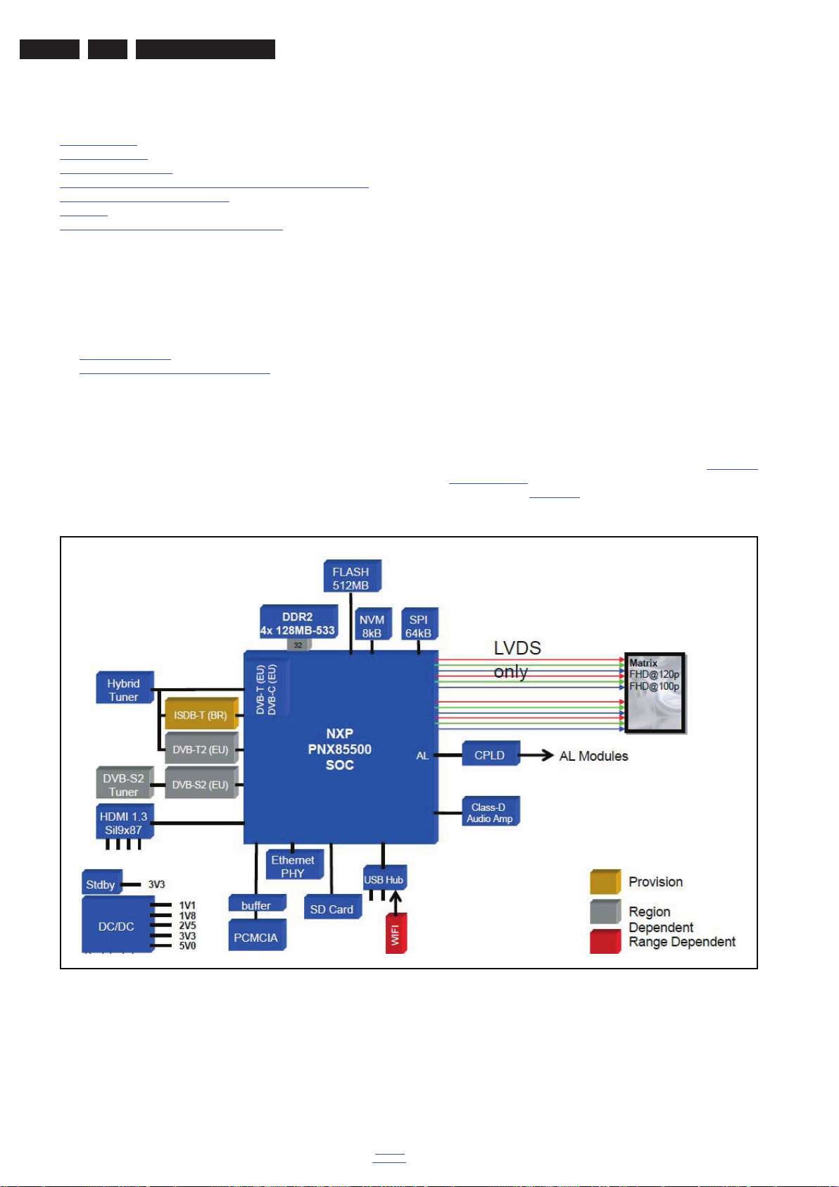
EN 48 Q552.2L LA7.
19110_053_110421.eps
110421
7. Circuit Descriptions
Circuit Descriptions
Index of this chapter:
7.1 Introduction
7.2 Power Supply
7.3 DC/DC Converters
7.4 Front-End Analogue and DVB-T, DVB-C; ISDB-T reception
7.5 Front-End DVB-S(2) reception
7.6 HDMI
7.7 Video and Audio Processing - PNX855xx
Notes:
•Only new circuits (circuits that are not published recently)
are described.
• Figures can deviate slightly from the actual situation, due
to different set executions.
• For a good understanding of the following circuit
descriptions, please use the wiring-, block- (see chapter
9. Block Diagrams
10. Circuit Diagrams and PWB Layouts
you will find a separate drawing for clarification.
) and circuit diagrams (see chapter
).Where necessary,
7.1 Introduction
The Q552.2L LA is part of the TV550 platform and uses the
(same) PNX855xx chipset.
The major deltas versus its predecessor Q551 are:
• support of DVB-T2 (“second generation” DVBT)
• implementation of “passive” 3D
• removal of TCON from the SSB (comes with the display)
• changed power architecture
• new USB hub (where applicable).
The Q552.2L LA chassis comes with the following stylings:
• Berlinale (series xxPFL58xx),
• Blockbuster (series xxPFL66xx),
• Emmy (series xxPFL76xx),
• Sundance (series xxPFL86xx).
7.1.1 Implementation
Key components of this chassis are:
• PNX855xx System-On-Chip (SOC) TV Processor
• TX26xx Hybrid Tuner (DVB-T/C, analogue)
• STV6110AT DVB-S Satellite Tuner
• SII9x87 HDMI Switch
• TPA312xD2PWP Class D Power Amplifier
• LAN8710 Dual Port Gigabit Ethernet media access
controller.
7.1.2 TV550 Architecture Overview
For details about the chassis block diagrams refer to chapter
Block Diagrams. An overview of the TV550 2011 architecture
can be found in Figure 7-1
.
9.
2011-Jul-15
Figure 7-1 Architecture of TV550 platform 2011
back to
div. table
Page 49
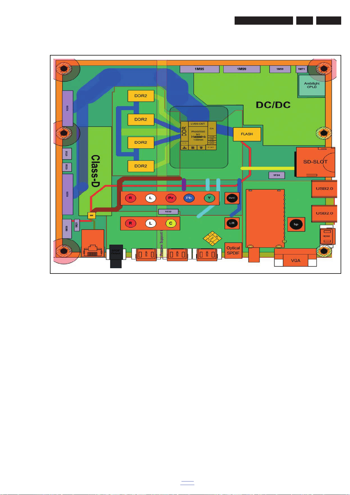
7.1.3 SSB Cell Layout
19110_052_110421.eps
110421
Circuit Descriptions
EN 49Q552.2L LA 7.
Figure 7-2 SSB layout cells (top view)
back to
div. table
2011-Jul-15
Page 50
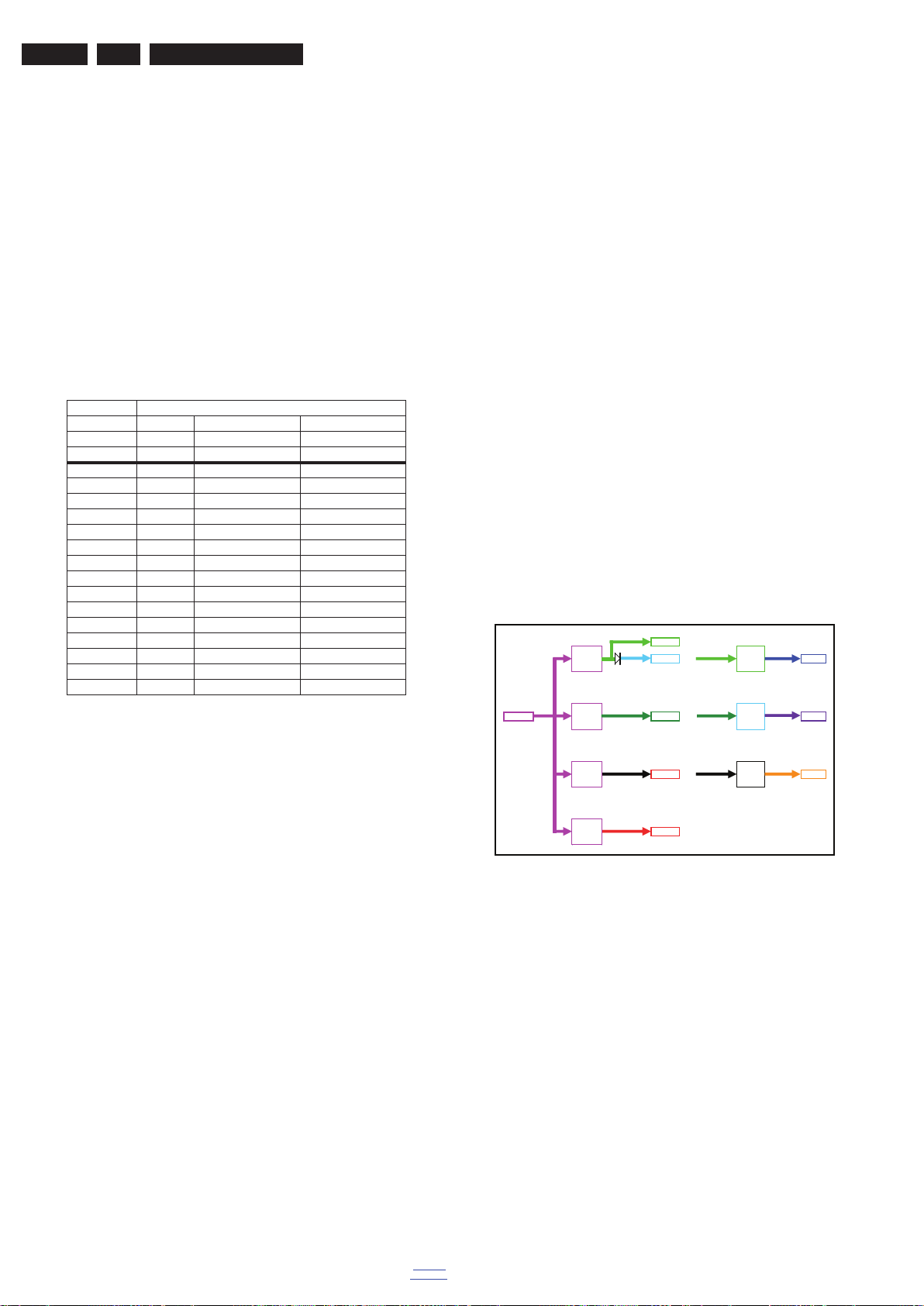
EN 50 Q552.2L LA7.
18770_226_100127.eps
100426
+5V5-TUN
196 mA
+5V
+5V5-TUN +5V-TUN
2179 mA 196 mA
+12V +3V 3
+3V3 +2V5
2919 mA 2371 m A 450 mA
+1V8
+1V8 +1V2
2450 mA 550 mA
+1V1
5100 mA
+1V1
dc-dc
+5V-TUN
stab ilizer
+2V5
stab ilizer
+1V2
stab ilizer
Circuit Descriptions
7.2 Power Supply
7.2.1 Power Supply Unit
All power supplies are a black box for Service. When defective,
a new board must be ordered and the defective one must be
returned, unless the main fuse of the board is broken. Always
replace a defective fuse with one with the correct
specifications! This part is available in the regular market.
Consult the Philips Service web portal for the order codes of the
boards.
In this manual, no detailed information is available because of
design protection issues.
7.2.2 Connector overview
Table 7-1 Connector overview
Connector
no. 1308 1316 1M95
Descr. Mains to display to SSB
Pin CN1 CN2 CN4
1 N Anode 1 +3V3stdby
2 L n.c. Standby
3 - Cathode 1 GND1
4-n.c. GND1
5 - Anode 2 +12V
6 - n.c. +12V
7 - Cathode 2 +Vsnd
8 - n.c. GND_SND
9 - Anode 3 BL-ON-OFF
10 - n.c. BL-DIM1 (Vsync)
11 - Cathode 3 BL-I-CTRL
12 - n.c. POK
13 - Anode 4 +24V (AL2_DVBS)
14 - n.c. GND1
15 - Cathode 4 -
7.3 DC/DC Converters
Stand-by microcontroller and ENABLE-3V3n is the signal
coming from the Stand-by microcontroller.
Diagram B03D contains the following linear stabilizers:
• +2V5 stabilizer, built around item no. 7UCO
• +5V-TUN stabilizer, built around items no. 7UA6 and 7UA7
• +1V2 stabilizer, built around items no. 7UA3 and 7UA4.
Diagram B08A contains the DVB-S2-related DC/DC
converters and -stabilizers:
• a +24V under-voltage detection circuitry is built around
item no. 7T04
• the switching frequency of the 24 to 14...20V switched
mode converter is 350 kHz (item no. 7T03 and +V-LNB
lines)
• the output signal on the +V-LNB line goes to the LNBH23Q
(item no. 7T50)
• the LNBH23Q (item no. 7T50) sends a feedback signal via
the V0-CNTRL line
• the switching frequency of the +5V-DVBS to +1-DVBS
switched mode converter is 900 kHz (item no. 7T00)
• a delay line for the +2V5-DVBS and +1V-DVBS lines is
created with item no. 3T03 (R=10k) and 2T06 (C=100n)
• a 3.3V to 2.5V linear stabilizer is built around item no. 7T01
• a 5V to 3.3V linear stabilizer is built around item no. 7T02.
Diagram B08B contains the DVB-S2 LNB supply:
• the +V-LNB signal comes from item no. 7T03
• the V0-CTRL signal goes to item no. 7T03
• the LNB-RF1 goes to the LNB.
Figures gives a graphical representation of the DC/DC
converters with its current consumptions:
+5V
dc-dc
+3V3
dc-dc
The on-board DC/DC converters deliver the following voltages
(depending on set execution):
• +3V3-STANDBY, permanent voltage for the Stand-by
controller, LED/IR receiver and controls; connector 1M95
pin 1
• +12V, input from the power supply for TV550 common
(active mode); connector 1M95 pins 6, 7 and 8
• +24V, input from the power supply for DVB-S2 (in active
mode); connector 1M09 pins 1 and 2
• +1V1, core voltage supply for PNX855xx; has to be started
up first and switched "off" last (diagram B03B)
• +1V2, supply voltage for analogue blocks inside PNX855xx
• +1V8, supply voltage for DDR2 (diagram B03B)
• +2V5, supply voltage for analogue blocks inside PNX855xx
(see diagram B03E)
• +3V3, general supply voltage (diagram B03E)
• +5V, supply voltage for USB and CAM (diagram B03E)
• +5V-TUN, supply voltage for tuner (diagram B03E)
• +V-LNB, input voltage for LNB supply IC (item no. 7T50)
• +5V-DVBS, input intermediate supply voltage for DVB-S2
• +3V3-DVBS, clean voltage for silicon tuner and DVB-S2
(diagram B08A)
channel decoder
• +2V5-DVBS, clean voltage for DVB-S2 channel decoder
• +1V-DVBS, core voltage for DVB-S2 channel decoder.
A +12 V under-voltage detector (see diagram B03C) enables
the 12V to 3.3V and 12V to 5V DC/DC converters via the
ENABLE-3V3-5V line, and the 12V to 1.8V DC/DC converter
via the ENABLE-1V8 line. DETECT2 is the signal going to the
+1V8
dc-dc
Figure 7-3 DC/DC converters
7.4 Front-End Analogue and DVB-T, DVB-C;
ISDB-T reception
7.4.1 Brazil region
The Front-End for the Brazil region consist of the following key
components:
• Hybrid Tuner with integrated SAW filter and amplifier
• External ISDB-T channel decoder covering the Brazilian
digital terrestrial TV standard
• Bandpass filter
•Amplifier
• PNX85500 SoC TV with integrated analogue demodulator.
Below find a block diagram of the front-end application for this
region.
2011-Jul-15
back to
div. table
Page 51
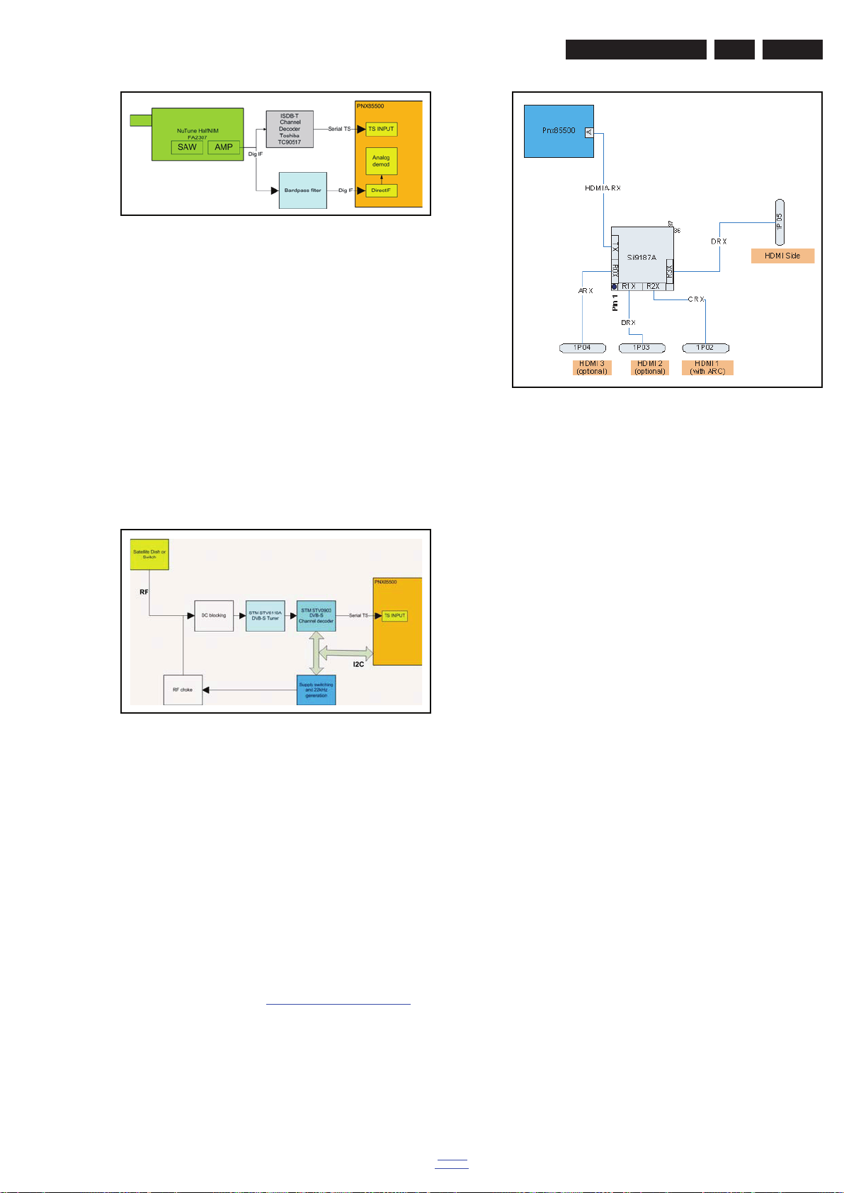
Figure 7-4 Front-End block diagram Brazil region
18770_236_100127.eps
100219
1
8770_237_100127.eps
100219
1
8770_243_100203.eps
100203
7.5 Front-End DVB-S(2) reception
The Front-End for the DVB-S(2) application consist of the
following key components:
Circuit Descriptions
EN 51Q552.2L LA 7.
• Satellite Tuner; I
decoder)
• Channel decoder; I
• LNB switching regulator; I
2
C address 0xC6 (bridged via channel
2
C address 0xD0
2
C address 0x14
• Amplifier
• PNX855xx SoC TV processor with integrated DVB-T and
DVB-C channel decoder and analogue demodulator.
Below find a block diagram of the front-end application for
DVB-S(2) reception.
Figure 7-5 Front-End block diagram DVB-S(2) reception
This application supports the following protocols:
• Polarization selection via supply voltage (18V = horizontal,
13V = vertical)
• Band selection via “toneburst” (22 kHz): tone “on” = “high”
band, tone “off” = “low” band
• Satellite (LNB) selection via DiSEqC 1.0 protocol
• Reception of DVB-S (supporting QPSK encoded signals)
and DVB-S2 (supporting QPSK, 8PSK, 16APSK and
32APSK encoded signals), introducing LDPC low-density
parity check techniques.
7.6 HDMI
In this platform, the Silicon Image Sil9x87 HDMI multiplexer is
implemented. Refer to figure 7-6 HDMI input configuration
the application.
for
Figure 7-6 HDMI input configuration
The following multiplexers can be used:
• Sil9187A (does not support “Instaport” technology for fast
switching between input signals)
• Sil9287B (supports “Instaport” technology for fast
switching between input signals).
The hardware default I
2
C addresses are:
• Sil9187A: 0xB0/0xB2 (random: software workaround)
• Sil9287B: 0xB2 (fixed).
The Sil9x87 has the following specifications:
• +5V detection mechanism
• Stable clock detection mechanism
• Integrated EDID
• RT control
• HPD control
• Sync detection
• TMDS output control
• CEC control
• EDID stored in Sil9x87, therefore there are no EDID pins
on the SSB.
7.7 Video and Audio Processing - PNX855xx
The PNX855xx is the main audio and video processor (or
System-on-Chip) for this platform. It has the following features:
• Multi-standard digital video decoder (MPEG-2, H.264,
MPEG-4)
• Integrated DVB-T/DVB-C channel decoder
• Integrated CI+
• Integrated motion accurate picture processing (MAPP2)
• High definition ME/MC
• 2D LED backlight dimming option
• Embedded HDMI HDCP keys
• Extended colour gamut and colour booster
• Integrated USB2.0 host controller
• Improved MPEG artefact reduction compared with
PNX8543
• Security for customers own code/settings (secure flash).
back to
div. table
The TV550 combines front-end video processing functions,
such as DVB-T channel decoding, MPEG-2/H.264 decode,
analog video decode and HDMI reception, with advanced
back-end video picture improvements. It also includes next
generation Motion Accurate Picture Processing (MAPP2). The
MAPP2 technology provides state-of-the-art motion artifact
reduction with movie judder cancellation, motion sharpness
2011-Jul-15
Page 52
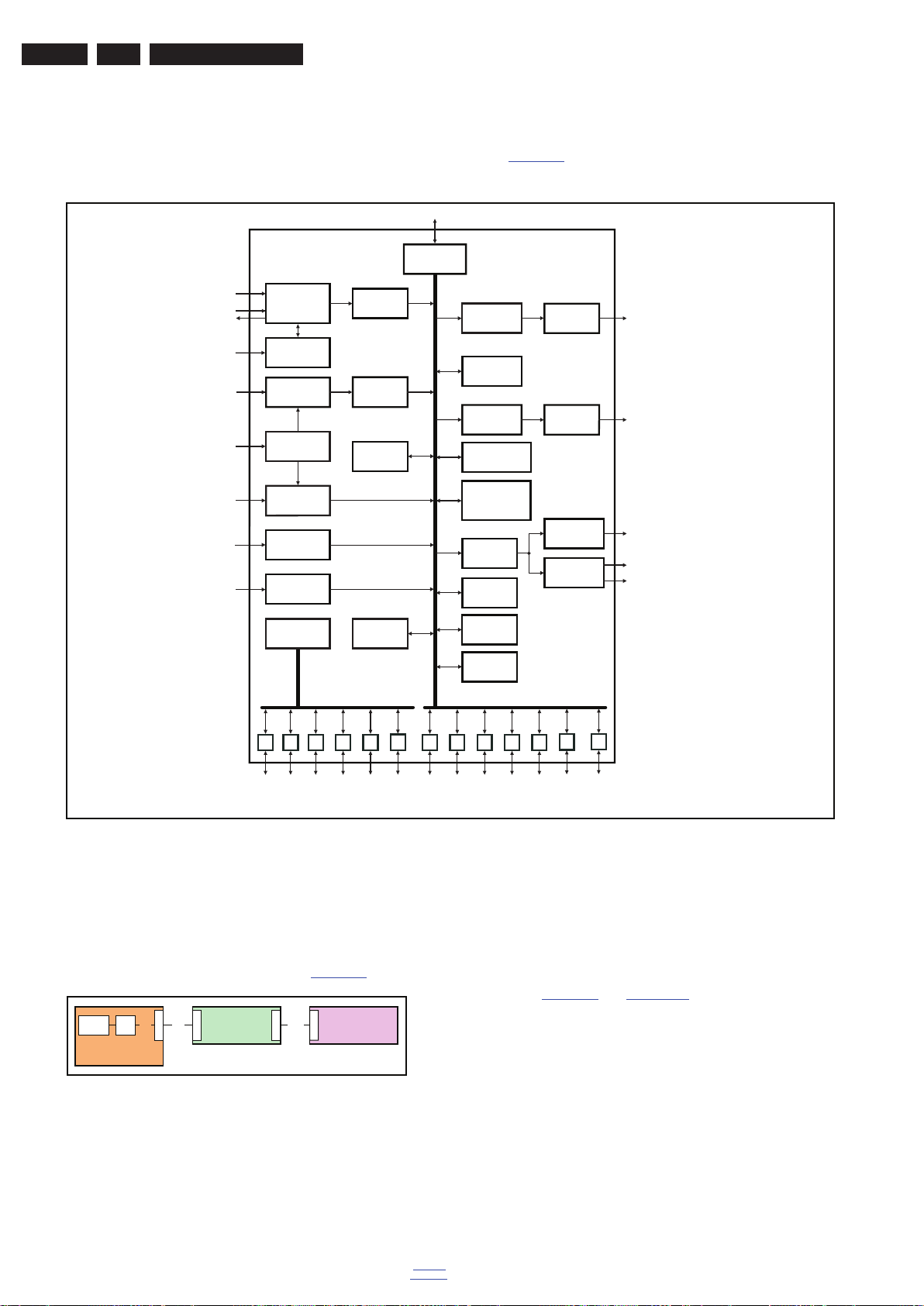
EN 52 Q552.2L LA7.
18770_241_100201.eps
100219
TS out/in for
TS input
CVBS, Y/C,
LVDS for
analog CVBS
SPDIF
Low-IF
SSIF, LR
HDMI
CI/CA
MPEG
PRIMARY
LVDS
VIDEO
SECONDARY
MEMORY
VIDEO
3D COMB
DIGITAL IF
AUDIO DEMOD
AUDIO IN
HDMI
SCALER,
AUDIO DSP
AUDIO DACS
AUDIO OUT
450 MHz
560 MHz
I2C
PWM
GPIO IR ADC UART I2C GPIO Flash
analog audio
I2S
SPDIF
SYSTEM
USB 2.0
PNX85500x
DVB-T/C
channel decoder
DVB
AV-PIP
SPI
MPEG/H.264
RECEIVER
(8051)
CONTROLLER
AND DECODE
DECODER
PCMCIA
RGB
PROCESSOR
SYSTEM
CONTROLLER
DECODER
VIDEO
24KEf CPU
MIPS32
x 8
AV-DSP
REDUCTION
AND NOISE
DE-INTERLACE
OUTPUT
VIDEO
SUB-PICTURE
ENCODER
OUTPUT
VIDEO
quad channel)
(single, dual or
flat panel display
DRAWING
ENGINE
DMA BLOCK
Motion-accurate
pixel processing
SD
Memory
Card
Ethernet
MAC
19111_009_110519.eps
110519
1
M
8
6
1
M
8
3
1
M
8
5
AmbiLight AmbiLight
PWM
CPLD
1
M
9
5
SSB
SPI
PNX85500
SPI
Circuit Descriptions
and vivid colour management. High flat panel screen
resolutions and refresh rates are supported with formats
including 1366 × 768 @ 100Hz/120Hz and 1920 × 1080 @
100Hz/120Hz. The combination of Ethernet, CI+ and H.264
supports new TV experiences with IPTV and VOD. On top of
that, optional support is available for 2D dimming in
combination with LED backlights for optimum contrast and
power savings up to 50%.
For a functional diagram of the PNX855xx, refer
to Figure 7-7
.
7.8 Ambilight
Sets in the xxPFL7606D/xx range are equipped with Ambilight.
For the implementation of Ambilight, refer to Figure 7-8
Figure 7-8 Ambilight configuration
Figure 7-7 PNX855xx functional diagram
.
with the CPLD located on the SSB whereas the Slave Ambilight
module communicates via the PWM communication protocol
with the Master Ambilight module.
The supply voltage of the modules is +24 V.
Refer to Figure 7-9
implementation.
and Figure 7-10 for the Ambilight board
2011-Jul-15
The Ambilight implementation consists of 2 separate units in
the set, where the Ambilight module located on the right (seen
from the back of the set) acts as a Master and the module on
the left acts as a Slave.
The NVM is located on the Master Ambilight module. This
module communicates via the SPI communication protocol
back to
div. table
Page 53
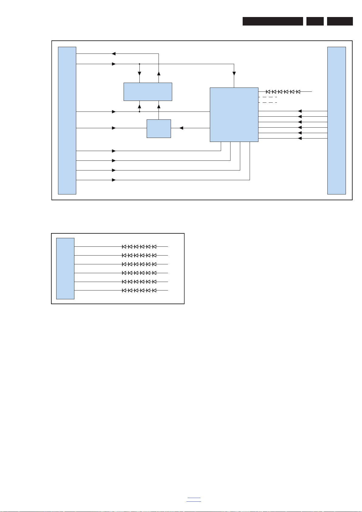
Circuit Descriptions
19111_010_110519.eps
110519
1M83
1M85
LED
Driver
OR
EEPROM
AMBI-SPI-SDI
AMBI-SPI-SDO
AMBI-SPI-CLK
PWM-G3
PWM-B3
PWM-R4
PWM-G4
PWM-B4
PWM-R3
+24 V
AMBI-SPI-CLK CS-Local
AMBI-PWM-CLK
AMBI-BLANK
AMBI-PROG
AMBI-LATCH
19111_011_110519.eps
110519
1M86
PWM-R3
+24 V
PWM-G3
+24 V
PWM-B3
+24 V
PWM-R4
+24 V
PWM-G4
+24 V
PWM-B4
+24 V
EN 53Q552.2L LA 7.
Figure 7-10 Slave Ambilight module
Figure 7-9 Master Ambilight module
back to
div. table
2011-Jul-15
Page 54
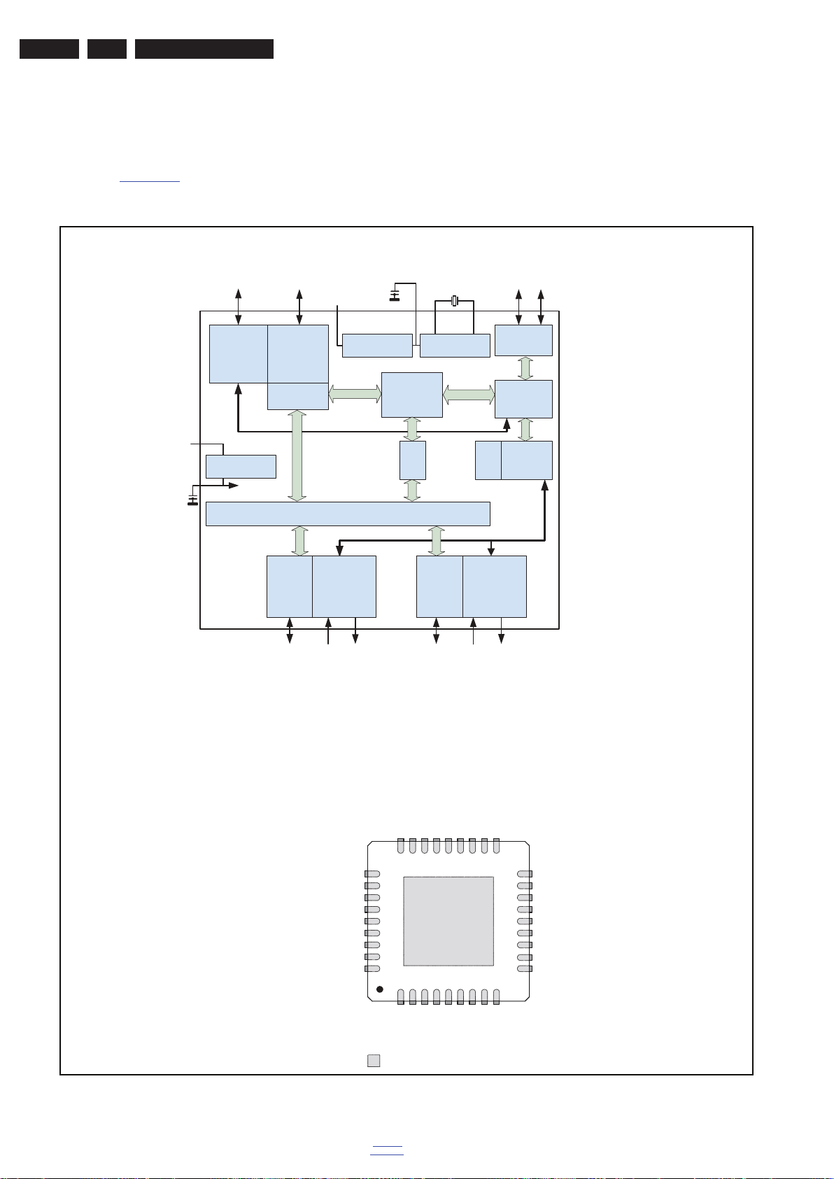
EN 54 Q552.2L LA8.
18770_301_100217.eps
100217
Block diagram
Pinning information
Note : The LED port indicators only apply to USB2513i.
To Upstream
V
BUS
3.3 V
Upstream
PHY
Upstream
USB Data
Repeater
Controller
Serial
Interface
Engine
Serial
Interface
To EEPROM or
SMBus Master
SCL
SDA
Port
Controller
Bus-
Power
Detect/
V
bus
Pulse
PHY#1
USB Data
Downstream
OC
Sense
Switch/
LED
Drivers
USB Data
Downstream
Port
Power
3.3 V
PLL
24 MHz
Crystal
Routing & Port Re-Ordering Logic
Regulator
CRFILT
Port
Power
Regulator
PHY#x
Port #x
OC Sense
Switch Driver/
LED Drivers
TT
#x
TT
#1
...
Port #1
OC Sense
Switch Driver/
LED Drivers
OC
Sense
Switch/
LED
Drivers
...
The ‘x’ indicates the number of available downstream ports: 2, 3, 4, or 7.
Ground Pad
(must be connected to VSS)
SMSC
USB2512/12A/12B
USB2512i/12Ai/12Bi
(Top View QFN-36)
26
VDD33
25
RESET_N24HS_IND / CFG_SEL[1]23SCL / SMBCLK / CFG_SEL[0]
22
SDA / SMBDATA / NON_REM[1]
21
NC
20
NC
19
VBUS_DET
27
NC
18
NC
17
OCS_N[2]
16
PRTPWR[2] / BC_EN[2]*
15
OCS_N[1]
14
VDD33
13
CRFILT
12
PRTPWR[1] / BC_EN[1]*
11
TEST
10
VDD33
SUSP_IND / LOCAL_PWR / NON_REM[0]
28
VDD33
29
USBDP_UP
31
XTALOUT
32
XTALIN / CLKIN
33
RBIAS
36
VDD33
35
PLLFILT
34
USBDM_UP
30
VDD33
1
USBDM_DN[1]
2
USBDP_DN[1]
3
USBDM_DN[2]
4
USBDP_DN[2]
5NC6
NC
7
NC
8NC9
Indicates pins on the bottom of the device.
8. IC Data Sheets
IC Data Sheets
This chapter shows the internal block diagrams and pin
configurations of ICs that are drawn as “black boxes” in the
8.1 Diagram USB Hub B01C, USB2513B (IC 7F25)
electrical diagrams (with the exception of “memory” and “logic”
ICs).
2011-Jul-15
Figure 8-1 Internal block diagram and pin configuration
back to
div. table
Page 55
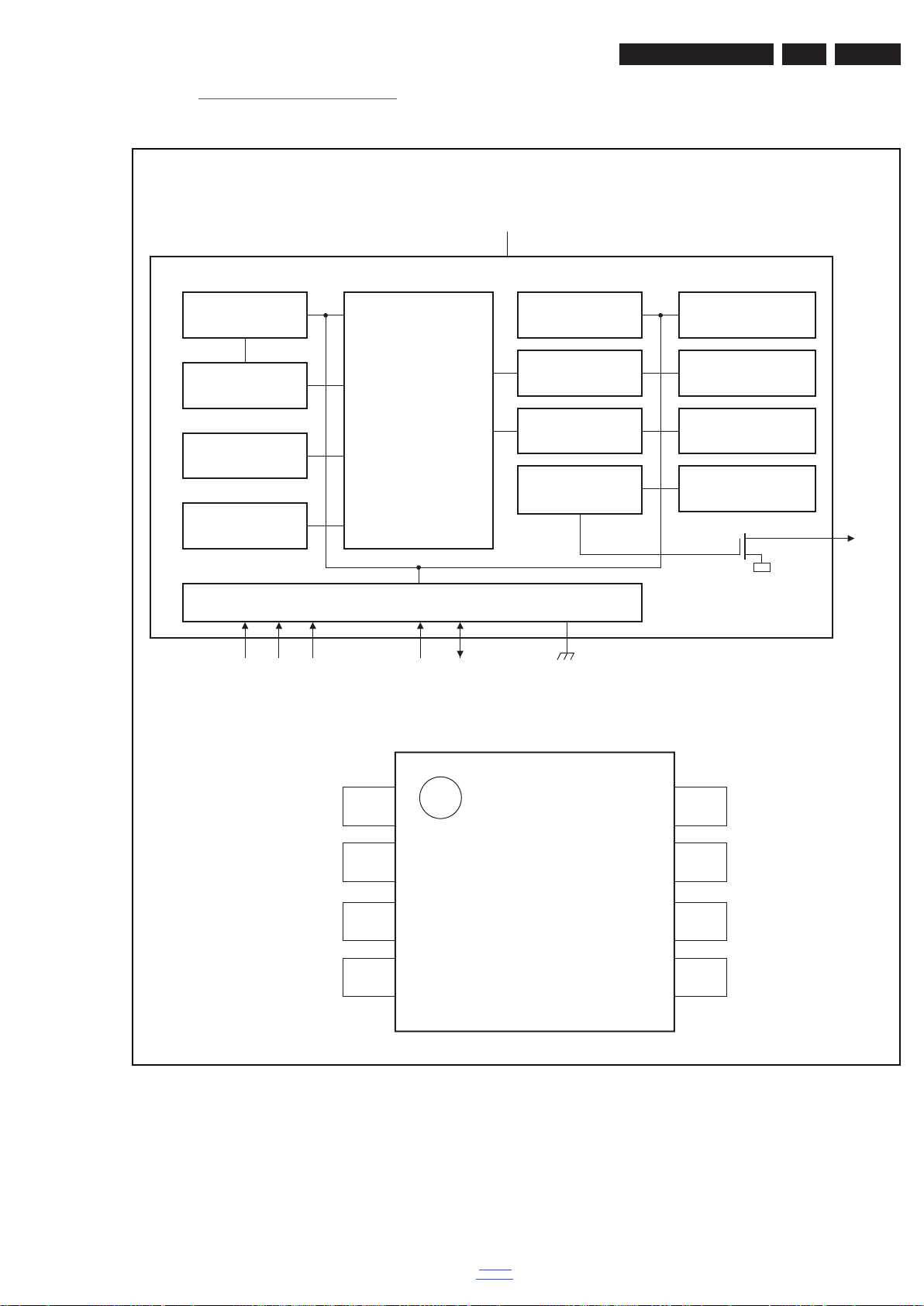
IC Data Sheets
8.2 Diagram Temp sensor & headphone B01J, LM75BDP (IC 7FD1)
Block diagram
V
CC
LM75B
EN 55Q552.2L LA 8.
BIAS
REFERENCE
BAND GAP
TEMP SENSOR
OSCILLATOR
POWER-ON
RESET
LOGIC CONTROL AND INTERFACE
Pinning information
11-BIT
SIGMA-DELTA
A-to-D
CONVERTER
SDA
SCLA0
POINTER
REGISTER
COUNTER
TIMER
COMPARATOR/
INTERRUPT
DNG1AA2
CONFIGURATION
REGISTER
TEMPERATURE
REGISTER
TOS
REGISTER
THYST
REGISTER
OS
1
2
3
4
LM75BDP
Figure 8-2 Pin configuration
8
7
6
5
VADS
CC
0ALCS
1ASO
2ADNG
18770_300_100217.eps
100217
back to
div. table
2011-Jul-15
Page 56
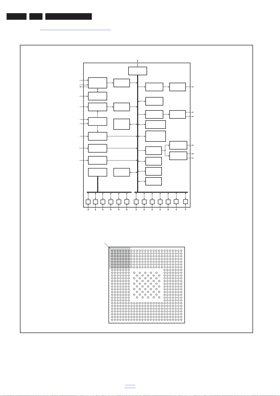
EN 56 Q552.2L LA8.
IC Data Sheets
8.3 Diagram NANDflash - conditional access B02A, PNX855xx (IC7S00)
Block diagram
TS input
TS out/in for
PCMCIA
DVB
CVBS, Y/C,
RGB
Low-IF
Direct-IF
SSIF, LR
SPDIF
HDMI
PNX8550x
CI/CA
DVB-T/C
channel decoder
VIDEO
DECODER
DIGITAL IF
AUDIO DEMOD
AND DECODE
AUDIO IN
HDMI
RECEIVER
SYSTEM
CONTROLLER
(8051)
MPEG
SYSTEM
PROCESSOR
3D COMB
MULTI-
STANDARD
VIDEO
DECODER
500 MHz
MIPS32
24KEf CPU
MEMORY
CONTROLLER
PRIMARY
VIDEO
OUTPUT
AV-PIP
SUB-PICTURE
SECONDARY
VIDEO
OUTPUT
Motion-accurate
pixel processing
SCALER,
DE-INTERLACE
AND NOISE
REDUCTION
AUDIO DSP
450 MHz
AV-DSP
DRAWING
ENGINE
Scatter/Gather
TS Demux
LVD S
VIDEO
ENCODER
AUDIO DACS
AUDIO OUT
LVD S fo r
flat panel display
(single, dual or
quad channel)
analog CVBS
analog Y/C
analog audio
I2S
SPDIF
Pinning information
Figure 8-3 Internal block diagram and pin configuration
PWM
I2C
Px_x IR ADC UART I2C GPIO Flash
SPI
ball A1
index area
246810121314
1357911
A
B
C
D
E
F
G
H
J
K
L
M
N
P
R
T
U
V
W
Y
AA
AB
AC
AD
AE
AF
Transparent top view
x 10
PNX8550xE
15 171619
18 20
USB 2.0
22 242526
23
21
SD
Memory
Card
Ethernet
MAC
18770_308_100217.eps
100217
2011-Jul-15
back to
div. table
Page 57
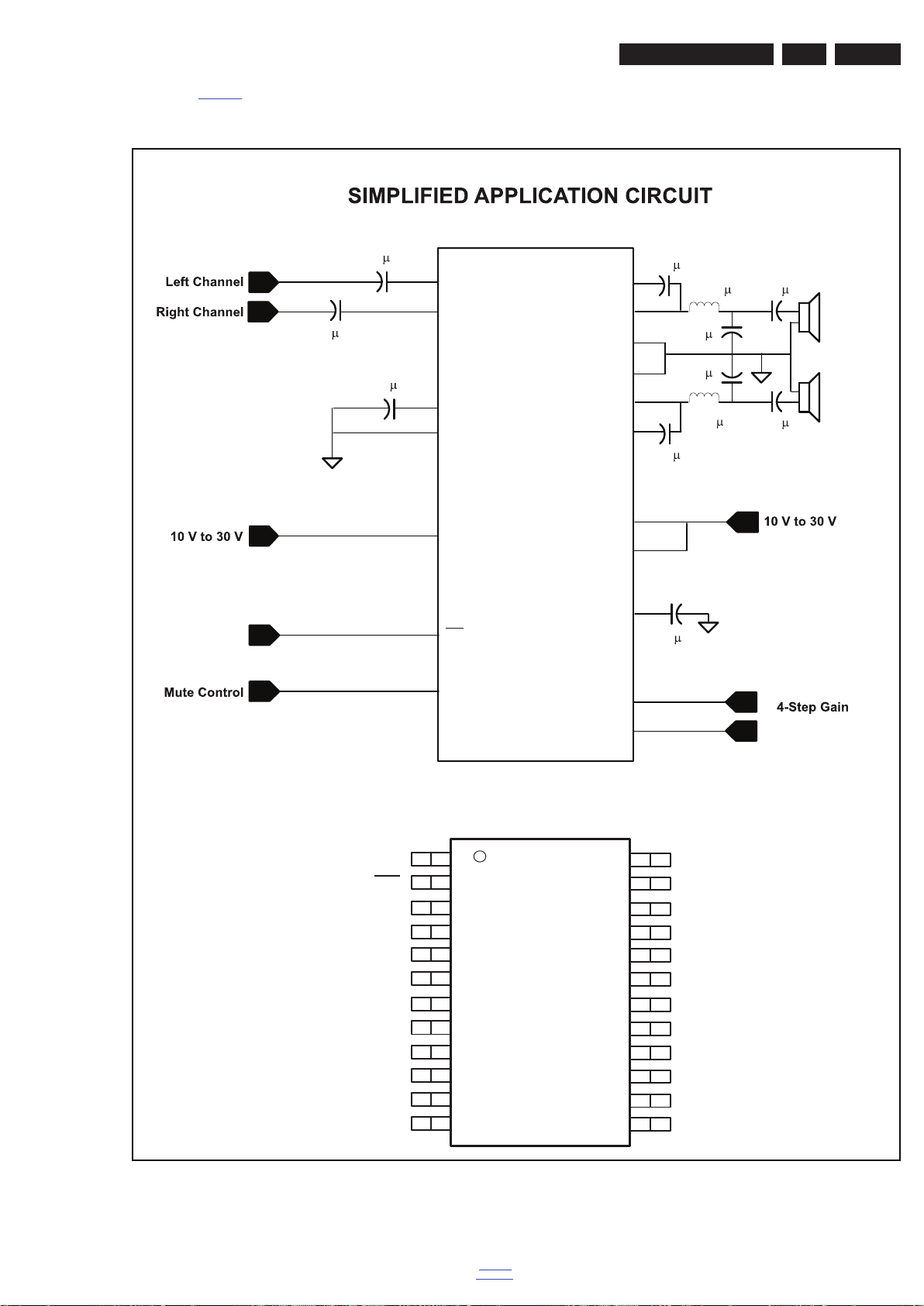
8.4 Diagram Audio B03A, TPA312xD2PWP (IC7D10)
Block diagram
1F
LIN
RIN
1F
IC Data Sheets
TPA3120D2
BSR
ROUT
PGNDR
0.22 F
22 H
0.68 F
EN 57Q552.2L LA 8.
470 F
Shutdown
Control
Pinning information
1F
PGNDL
BYPASS
AGND
AVCC
SD
MUTE
LOUT
BSL
PVCCL
PVCCR
VCLAMP
GAIN0
GAIN1
PWP (TSSOP) PACKAGE
(TOP VIEW)
0.22 F
1F
0.68 F
22 H
470 F
}
Control
PVCCL
SD
PVCCL
MUTE
LIN
RIN
BYPASS
AGND
AGND
PVCCR
VCLAMP
PVCCR
Figure 8-4 Internal block diagram and pin configuration
1
2
3
4
5
6
7
8
9
10
11
12
back to
div. table
24
23
22
21
20
19
18
17
16
15
14
13
PGNDL
PGNDL
LOUT
BSL
AVCC
AVCC
GAIN0
GAIN1
BSR
ROUT
PGNDR
PGNDR
I_18020_142.eps
100402
2011-Jul-15
Page 58
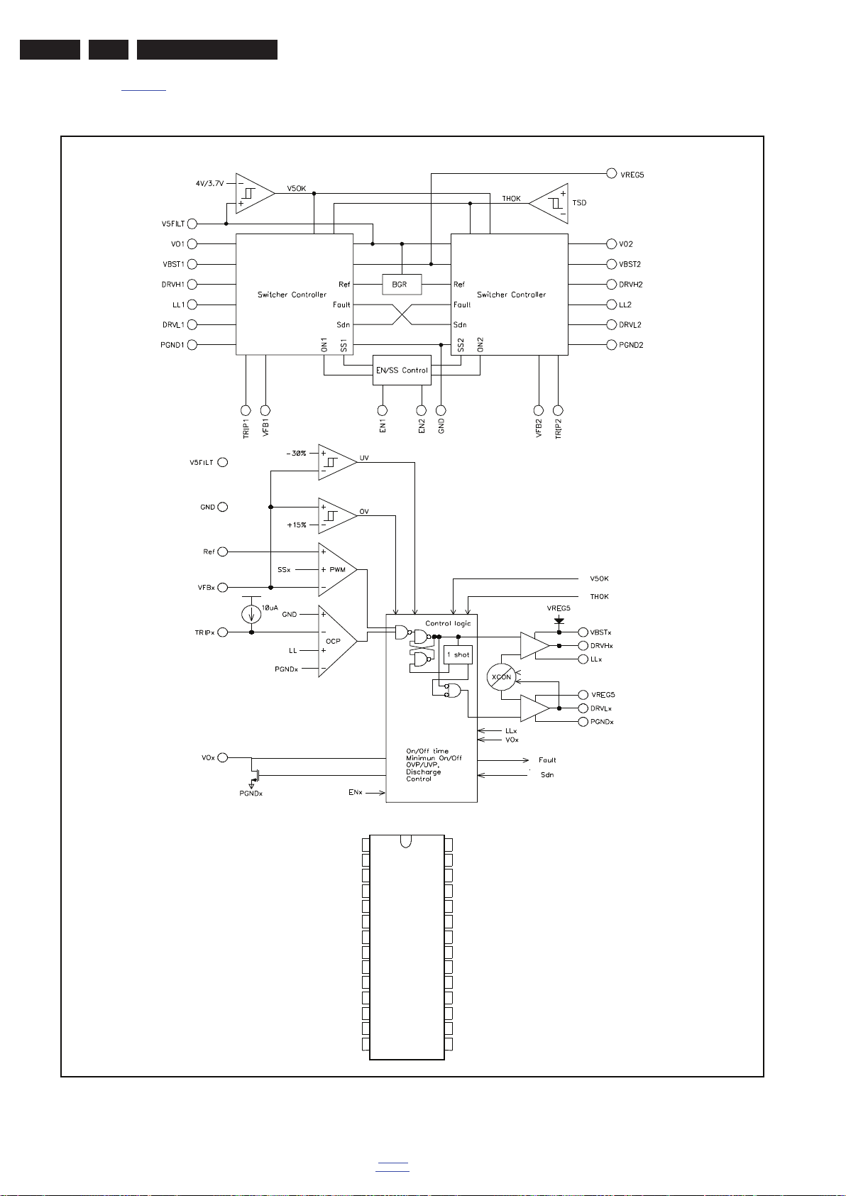
EN 58 Q552.2L LA8.
IC Data Sheets
8.5 Diagram DC/DC B03B, TPS53126PW (IC7U03)
Block diagram
2011-Jul-15
Pinning information
Figure 8-5 Internal block diagram and pin configuration
VBST1
EN1
VO1
VFB1
GND
TEST1
VFB2
VO2
EN2
VBST2
28
1
NC
2
3
4
5
6
7
8
9
10
11
12
13
14
back to
div. table
TPS53124
NC
NC
NC
DRVH1
27
LL1
26
DRVL1
25
PGND1
24
TRIP1
23
VIN
VREG5
22
21
V5FILT
TEST2
20
TRIP2
19
PGND2
18
DRVL2
17
LL2
16
DRVH2
15
18310_300_090319.eps
100416
Page 59
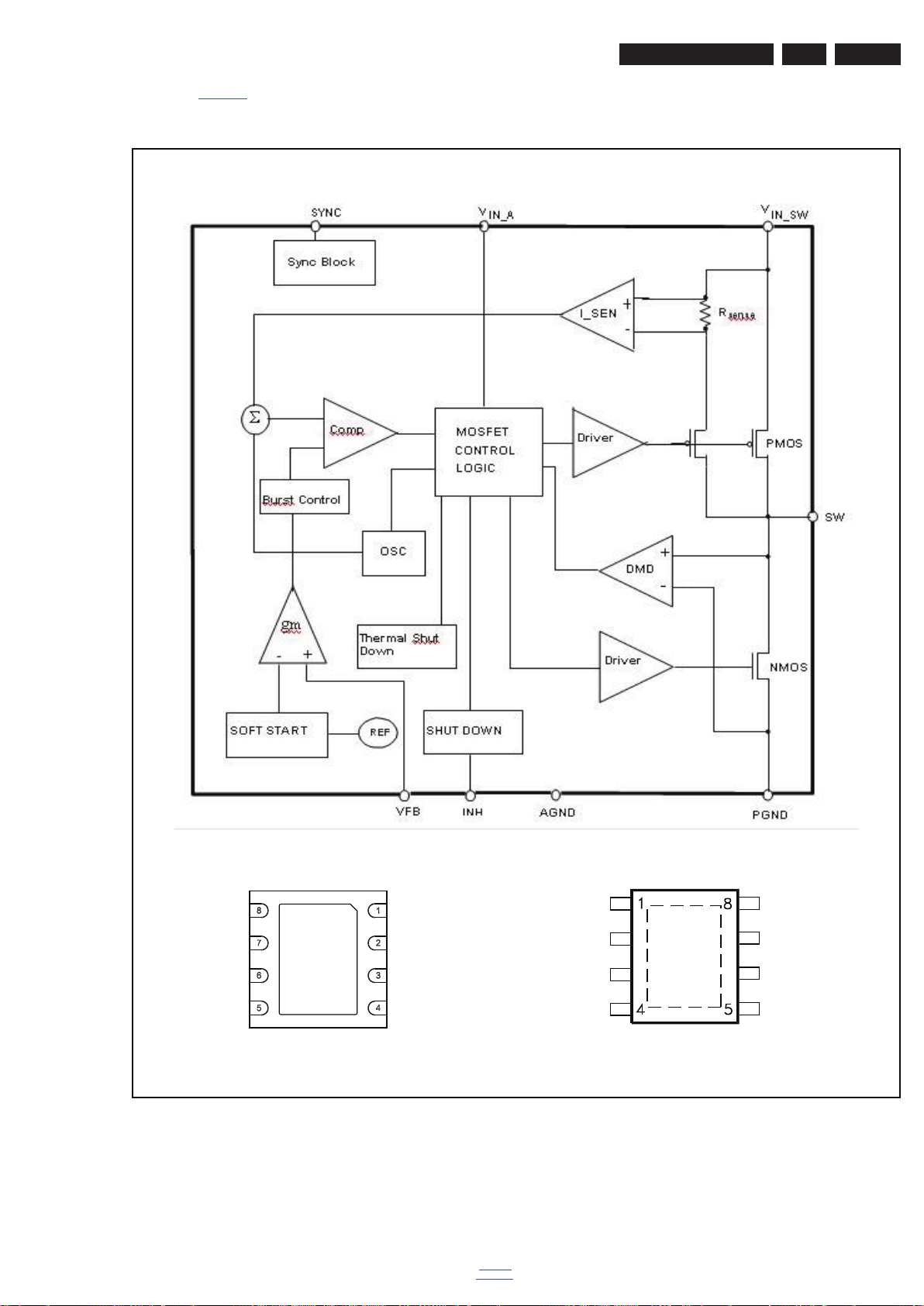
8.6 Diagram DC/DC B03E, ST1S10PH (IC 7UD0)
Block diagram
ST1S10PH
IC Data Sheets
EN 59Q552.2L LA 8.
Pinning information
DFN8 (4 × 4)
Figure 8-6 Internal block diagram and pin configuration
back to
div. table
PowerSO-8
I_18010_083.eps
110601
2011-Jul-15
Page 60
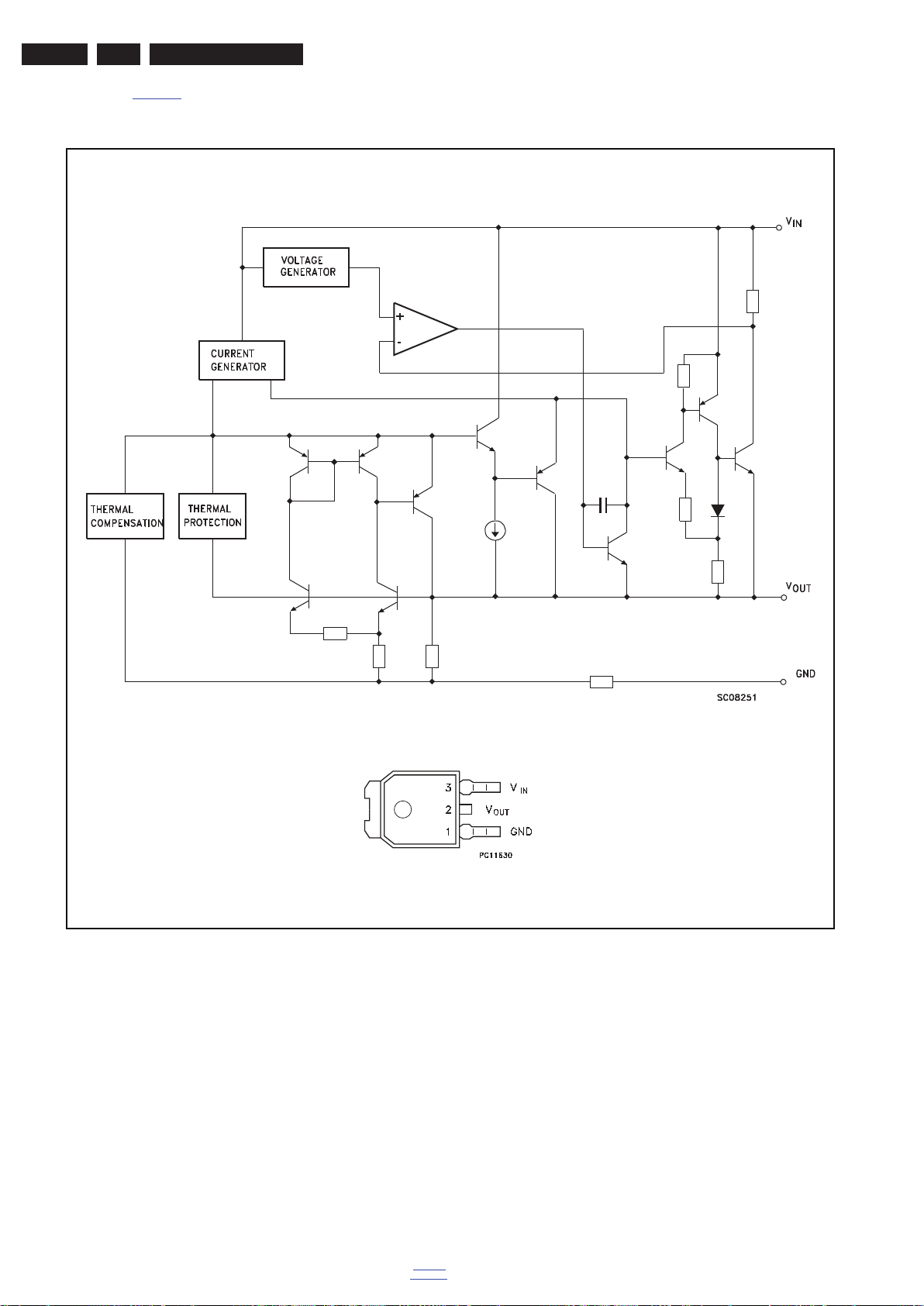
EN 60 Q552.2L LA8.
IC Data Sheets
8.7 Diagram DC/DC B03E, LD1117DT25 (IC 7UD2)
Block diagram
LD1117DT
Pinning information
Figure 8-7 Internal block diagram and pin configuration
DPAK
F_15710_166.eps
100402
2011-Jul-15
back to
div. table
Page 61
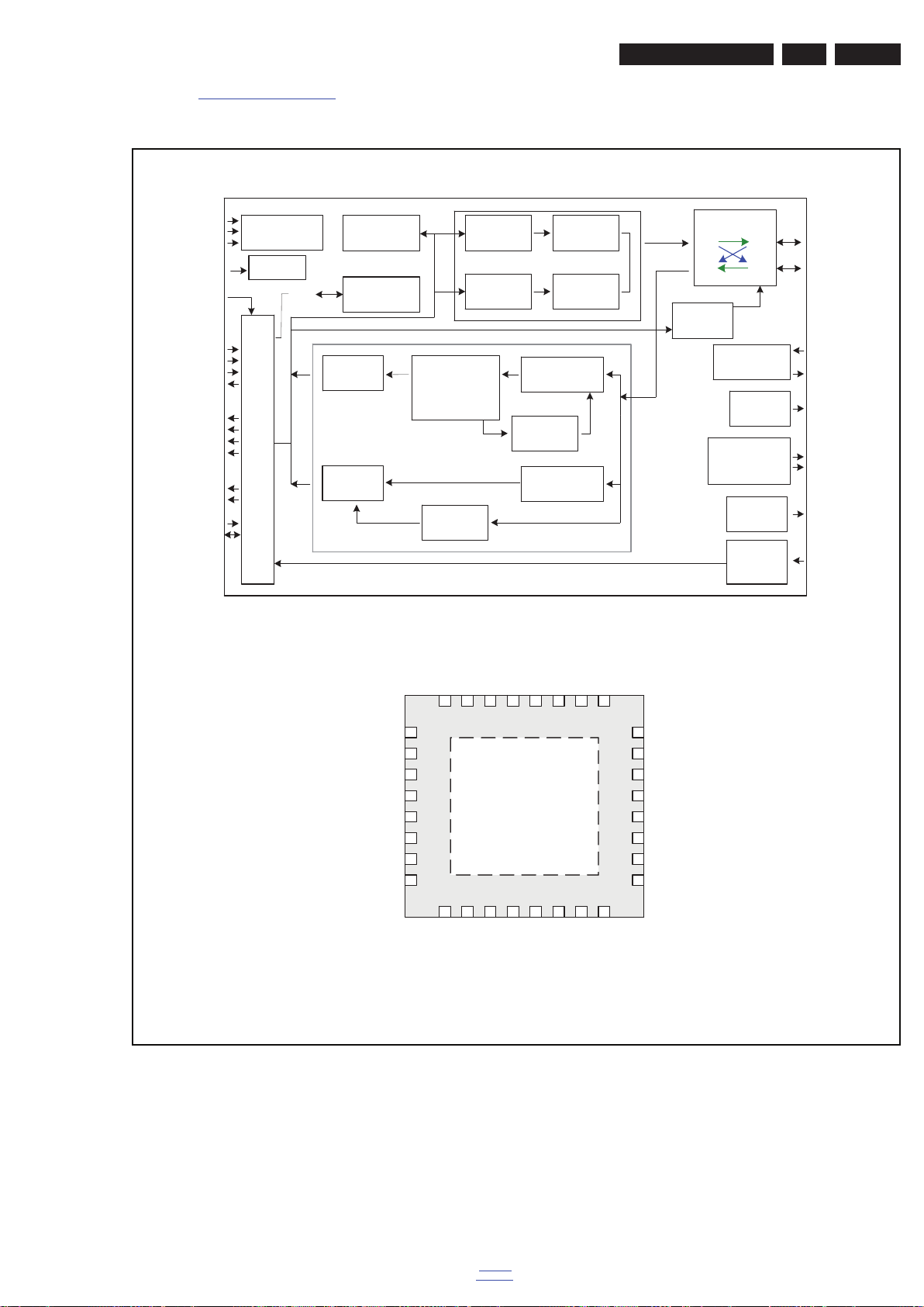
IC Data Sheets
8.8 Diagram Ethernet & Service B04C, LAN8710A-EZKH (IC 7E10)
Block diagram
EN 61Q552.2L LA 8.
MODE0
MODE1
MODE2
nRST
RMIISEL
TXD[0:3]
TXEN
TXER
TXCLK
RXD[0:3]
RXDV
RXER
RXCLK
CRS
COL/CRS_DV
MDC
MDIO
MODE Control
Reset
Control
SMI
100M Rx
Logic
RMII / MII Logic
10M Rx
Logic
Pinning information
Auto-
Negotiation
Management
Control
DSP System:
Data Recovery
Receive Section
Clock
Equalizer
10M PLL
10M Tx
Logic
Transmit Section
100M Tx
Logic
Analog-to-
100M PLL
Squelch &
10M
Transmitter
100M
Transmitter
Digital
Filters
HP Auto-MDIX
MDIX
Control
LED Circuitry
PLL
Interrupt
Generator
Central
Bias
PHY
Address
Latches
TXP / TXN
RXP / RXN
XTAL1/CLKIN
XTAL2
nINT
LED1
LED2
RBIAS
PHYAD[0:2]
TXP
RXN
RXP
30
29
31
SMSC
32 PIN QFN
(Top View)
VSS
10
12
11
VDDIO
RXD0/MDE0
RXD1/MODE1
TXN
28
13
RXER/RXD4/PHYAD0
27
14
CRS
RXDV
26
15
COL/CRS_DV/MODE2
2516
24
23
22
21
20
19
18
17
MDIO
VDD2A
LED2/nINTSEL
LED1/REGOFF
XTAL2
XTAL1/CLKIN
VDDCR
RXCLK/PHYAD1
RXD3/PHYAD2
RBIAS
32
1
2
3
4
LAN8710/LAN8710i
5
6
7
8
9
RXD2/RMIISEL
TXD3
VDD1A
Figure 8-8 Internal block diagram and pin configuration
TXD2
TXD1
TXD0
TXEN
TXCLK
nRST
nINT/TXER/TXD4
MDC
18770_302_100217.eps
100217
back to
div. table
2011-Jul-15
Page 62
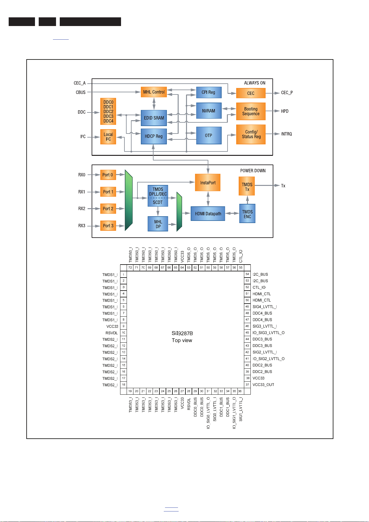
EN 62 Q552.2L LA8.
18770_303_100217.eps
100217
Block diagram
Pinning information
IC Data Sheets
8.9 Diagram HDMI B04D, SII9x87B (IC 7EC1)
Figure 8-9 Internal block diagram and pin configuration
2011-Jul-15
back to
div. table
Page 63
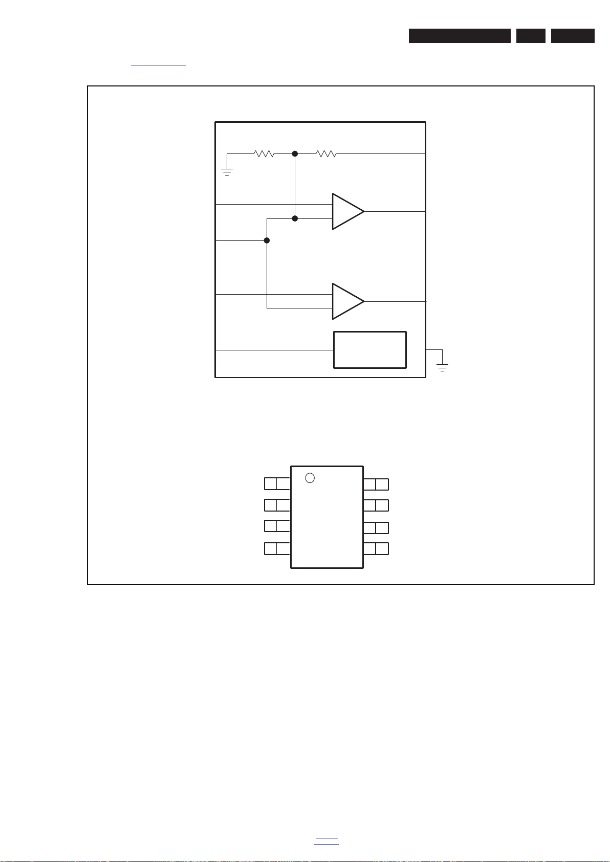
IC Data Sheets
8.10 Diagram Headphone B04E, TPA6111A2DGN (IC 7EE1)
Block diagram
/2
V
DD
IN1−
2
BYP
3
6
ASS
IN2−
−
+
TPA6111A2
−
+
EN 63Q552.2L LA 8.
8
V
DD
V
1
O1
V
7
O2
SHUTDOWN
5
Pinning information
BYPASS
GND
Figure 8-10 Internal block diagram and pin configuration
D OR DGN PACKAGE
(TOP VIEW)
V
O1
IN1−
1
2
3
4
Bias
Control
8
7
6
5
4
V
DD
V
O2
IN2−
SHUTDOWN
18770_309_100217.eps
110602
back to
div. table
2011-Jul-15
Page 64
EN 64 Q552.2L LA8.
P
ersonal Notes:
IC Data Sheets
2011-Jul-15
back to
div. table
10000_012_090121.eps
090121
Page 65
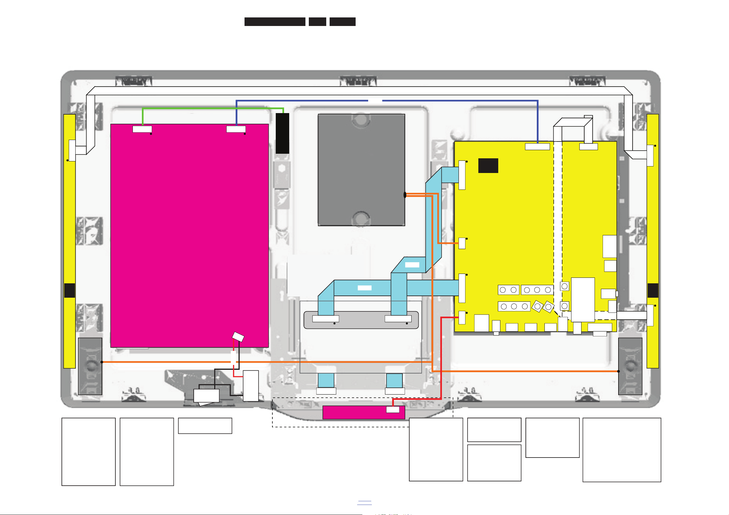
Block Diagrams
EN 65Q552.2L LA 9.
2011-Jul-15
back to
div. table
9. Block Diagrams
9-1 Wiring diagram Blockbuster/Emmy 32"
LCD DISPLAY
(1004)
MAIN POWER SUPPLY
32
"
PLDC-P005A
(1005)
LOUDSPEAKER
(5213)
LOUDSPEAKER
(5216)
LOUDSPEAKER
(5216)
1M19
8P
1D38
3P
1M95
14P
1M59
26P
SD-CARD
READER
USB
ETHER
NET
SPDIF
HDMIHDMIHDMI
VGA
1316
10P
1M95
14P
MAINS
SWITCH
(8308)
INLET
8M95
19110_008_110323.eps
110711
TO DISPLAY
51P
TO DISPLAY
41P
C2 C1
IR/LED/CONTROL BOARD
(1108)
J1
8P
WIRING DIAGRAM 32" BLOCKBUSTER / EMMY
1M19
(B09A)
1. LIGHT-SENSOR
2. GND
3. RC
4. LED-2
5. +3V3-STANDBY
6. LED-1
7. KEYBOARD
8. +5V
1735
(B03A)
1. LEFT-SPEAKER
2. GND-AUDIO
3. GND-AUDIO
4. RIGHT-SPEAKER
1D38
(B03A)
1. LEFT-SPEAKER
2. GND-AUDIO
3. RIGHT-SPEAKER
1308
(PSU)
1. N
2. L
1M95
(B03C)
1. +3V3-STANDBY
2. STANDBY
3. GND
4. GND
5. +12VIN
6. +12VIN
7. +24V-AUDIO-POWER
8. GND
9. LAMP-ON
10. BACKLIGHT-PWM_BL-VS
11. BACKLIGHT-BOOST
12. POWER-OK
13. +24V
14. GND
1M95
(PSU)
1. +3V3STDBY
2. STANDBY
3. GND
4. GND
5. +12V
6. +12V
7. +VSND
8. GND_SND
9. BL-ON-OFF
10. BL-DIM1
11. BL-I-CTRL
12. POK
13. +24V
14. GND1
1316
(PSU)
1. ANODE 1
2. NC
3. CATHODE 1
4. GND
5. ANODE 2
6. NC
7. CATHODE 2
8. NC
9. ANODE 3
10. NC
11. CATHODE 3
12. NC
13. ANODE 4
14. NC
15. CATHODE 4
1G51
(B06B)
1. +VDISP
2. +VDISP
3. +VDISP
4. +VDISP
|
|
51. CTRL-DISP
TO DISPLAY
SUPPLY
8308
1G50
41P
1G51
51P
2P
13
08
*AMBILIGHT MODULE
(1162)
AL
18P
1M86
*AMBILIGHT MODULE
(1161)
AL
1M85
18P
1M83
26P
TUNER
SPDIF
PHONE
8M85
8M59
8G51
8G50
SSB
3139 123 6521.x
(1150)
B
*AMBILIGHT ONLY APLICABLE FOR EMMY STYLING
1M59
(B09A)
1. AMBI-SPI-CLK-OUT
2. GND
3. AMBI-SPI-SDO-OUT
4. AMBI-SPI-SDI-OUT-GI
5. V-AMBI
6. AMBI-PWM-CLK_B2
7. GND
8. AMBI-SPI-CS-OUTn_R2
9. AMBI-LATCH1_G2
10. V-AMBI
11. AMBI-BLANK_R1
12. AMBI-PROG_B1
13. AMBI-LATCH2_DIS
14. AMBI-TEMP
15. GND_AL
16. GND_AL
17. GND_AL
18. GND_AL
19. GND_AL
20. N.C.
21. +24V
22. +24V
23. +24V
24. +24V
25. +24V
26. +24V
LEADING EDGE
HDMI
Page 66
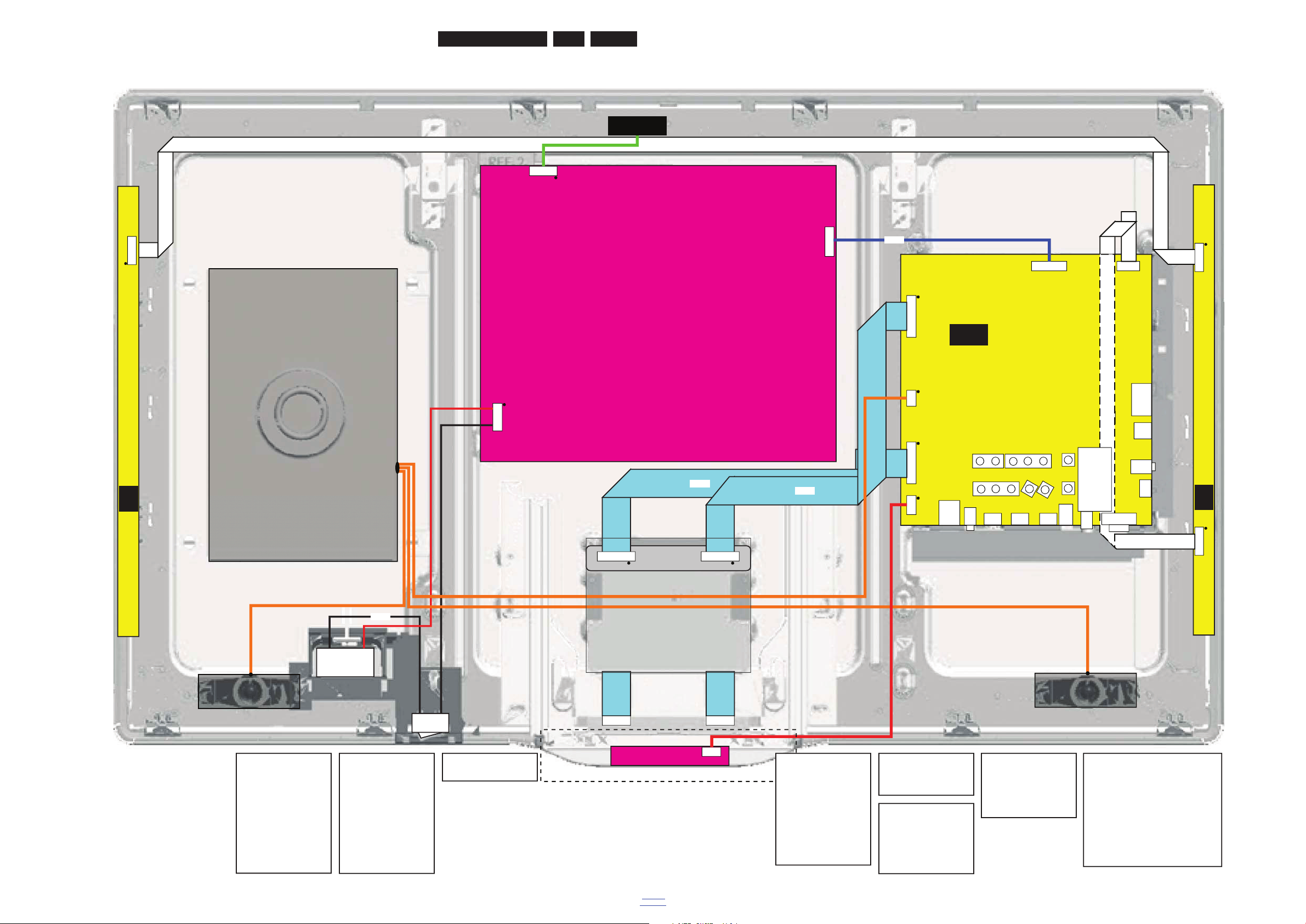
EN 66Q552.2L LA 9.
Block Diagrams
2011-Jul-15
back to
div. table
9-2 Wiring diagram Blockbuster/Emmy 40" - 46"
LCD DISPLAY
(1004)
MAIN POWER SUPPLY
40
"
PLDE-P008A
46
"
PLDG-P010A
(1005)
LOUDSPEAKER
(5213)
LOUDSPEAKER
(5216)
LOUDSPEAKER
(5216)
1M19
8P
1D38
3P
1M95
14P
1M59
26P
1G50
41P
1G51
51P
SSB
3139 123 6521.x
(1150)
B
SD-CARD
READER
USB
ETHER
NET
SPDIF
PHONE
SPDIF
HDMI
HDMIHDMIHDMI
1316
10P
MAINS
SWITCH
(8308)
14P
1M99
1308
2P
INLET
8308
8M95
8G51
8G50
19110_009_110323.eps
110711
TO DISPLAY
51P
TO DISPLAY
41P
C2 C1
IR/LED/CONTROL BOARD
(
1108
)
J1
8P
WIRING DIAGRAM 40"- 46" BLOCKBUSTER / EMMY
1M19 (B09A)
1. LIGHT-SENSOR
2. GND
3. RC
4. LED-2
5. +3V3-STANDBY
6. LED-1
7. KEYBOARD
8. +5V
1D38 (B03A)
1. LEFT-SPEAKER
2. GND-AUDIO
3. RIGHT-SPEAKER
1308 (PSU)
1. N
2. L
1M95 (PSU)
1. +3V3STDBY
2. STANDBY
3. GND
4. GND
5. +12V
6. +12V
7. +VSND
8. GND_SND
9. BL-ON-OFF
10. BL-DIM1
11. BL-I-CTRL
12. POK
13. +24V
14. GND1
1316 (PSU)
1. ANODE 1
2. NC
3. CATHODE 1
4. GND
5. ANODE 2
6. NC
7. CATHODE 2
8. NC
9. ANODE 3
10. NC
11. CATHODE 3
12. NC
13. ANODE 4
14. NC
15. CATHODE 4
1G51 (B06B)
1. +VDISP
2. +VDISP
3. +VDISP
4. +VDISP
|
|
51. CTRL-DISP
TO DISPLY
SUPPLT
LEADING EDGE
1M59 (B09A)
1. AMBI-SPI-CLK-OUT
2. GND
3. AMBI-SPI-SDO-OUT
4. AMBI-SPI-SDI-OUT-GI
5. V-AMBI
6. AMBI-PWM-CLK_B2
7. GND
8. AMBI-SPI-CS-OUTn_R2
9. AMBI-LATCH1_G2
10. V-AMBI
11. AMBI-BLANK_R1
12. AMBI-PROG_B1
13. AMBI-LATCH2_DIS
14. AMBI-TEMP
15. GND_AL
16. GND_AL
17. GND_AL
18. GND_AL
19. GND_AL
20. N.C.
21. +24V
22. +24V
23. +24V
24. +24V
25. +24V
26. +24V
1M95 (B03C)
1. +3V3-STANDBY
2. STANDBY
3. GND
4. GND
5. +12VIN
6. +12VIN
7. +24V-AUDIO-POWER
8. GND
9. LAMP-ON
10. BACKLIGHT-PWM_BL-VS
11. BACKLIGHT-BOOST
12. POWER-OK
13. +24V
14. GND
*AMBILIGHT MODULE 24 LED
(1162)
AL
18P
1M86
*AMBILIGHT MODULE 24 LED
(1161)
AL
1M85
18P
1M83
26P
TUNER
8M59
VGA
*AMBILIGHT ONLY APLICABLE FOR EMMY STYLING
Page 67
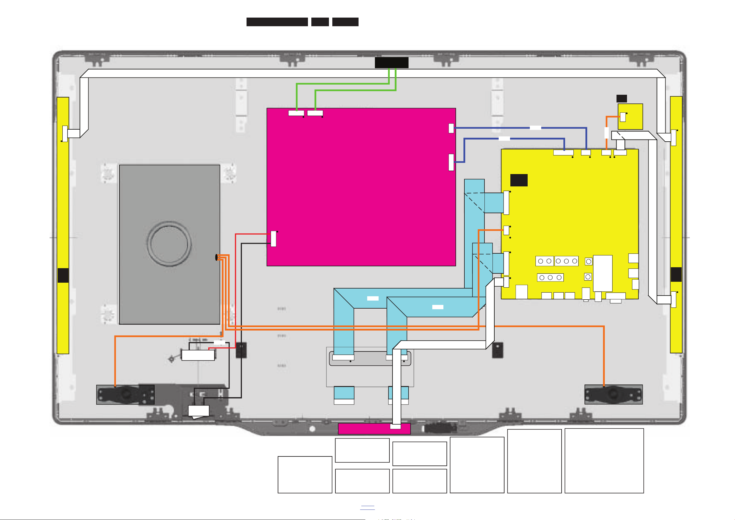
Block Diagrams
EN 67Q552.2L LA 9.
2011-Jul-15
back to
div. table
9-3 Wiring diagram Sundance 42" - 47"
LCD DISPLAY
(1004)
MAIN POWER SUPPLY
42
" - 47"
PLDHP018A
(1005)
LOUDSPEAKER
(5213)
LOUDSPEAKER
(5216)
LOUDSPEAKER
(5217)
1M20
11P
1D38
3P
1T02
4P
1M95
14P
1M994P1M714P1M59
26P
1G50
41P
1G51
51P
SSB
3139 123 6521.x
(1150)
B
USB USB
ETHER
NET
HDMI
HDMIHDMIHDMI
1316
10P
1319
10P
MAINS
SWITCH
(8308)
14P
1M99
4P
1M09
1308
2P
INLET
8308
8M95
8G50
19110_063_110711.eps
110711
TO DISPLAY
41P
TO DISPLAY
51P
CN2CN1
IR/LED/CONTROL BOARD
(1108)
J1
11P
WIRING DIAGRAM 42"- 47" SUNDANCE
1M20 (B09A)
1. LIGHT-SENSOR
2. LED-1
3. LED-2
4. GND
5. KEYBOARD
6. +3V3-STANDBY
7. RC
8. +5V
9. SCL-SET
10. GND
11. SDA-SET
1D38 (B03A)
1. LEFT-SPEAKER
2. GND-AUDIO
3. RIGHT-SPEAKER
1G51 (B06B)
1. +VDISP
2. +VDISP
3. +VDISP
4. +VDISP
|
|
51. N.C.
LED
POWER
1M59 (B09A)
1. AMBI-SPI-CLK-OUT
2. GND
3. AMBI-SPI-SDO-OUT
4. AMBI-SPI-SDI-OUT-GI
5. V-AMBI
6. AMBI-PWM-CLK_B2
7. GND
8. AMBI-SPI-CS-OUTn_R2
9. AMBI-LATCH1_G2
10. V-AMBI
11. AMBI-BLANK_R1
12. AMBI-PROG_B1
13. AMBI-LATCH2_DIS
14. AMBI-TEMP
15. GND_AL
16. GND_AL
17. GND_AL
18. GND_AL
19. GND_AL
20. N.C.
21. +12V_AL
22. +12V_AL
23. +12V_AL
24. +12V_AL
25. +12V_AL
26. +12V_AL
1M95 (B03C)
1. +3V3-STANDBY
2. STANDBY
3. GND
4. GND
5. +12VIN
6. +12VIN
7. +24V-AUDIO-POWER
8. GND
9. LAMP-ON
10. BACKLIGHT-PWM_BL-VS
11. BACKLIGHT-BOOST
12. POWER-OK
13. +24V
14. GND
AMBILIGHT MODULE
(1163)
AL
26P
1M83
AMBILIGHT MODULE
(1163)
AL
1M84
26P
1M83
26P
TUNER
VGA
8G51
8M84
8M59
WIFI MODULE
(1115)
8M99
1735 (B03A)
1. LEFT-SPEAKER
2. GND-AUDIO
3. GND-AUDIO
4. RIGHT-SPEAKER
1M99 (B03C)
1. GND_AL
2. +12V_AL
3. GND_AL
4. +12V_AL
1M71 (B09A)
1. SCL-BL
2. GND
3. SDA-BL
4. +3V3
8M71
8M21
TEMP. SENSOR
(1027)
TS
Page 68
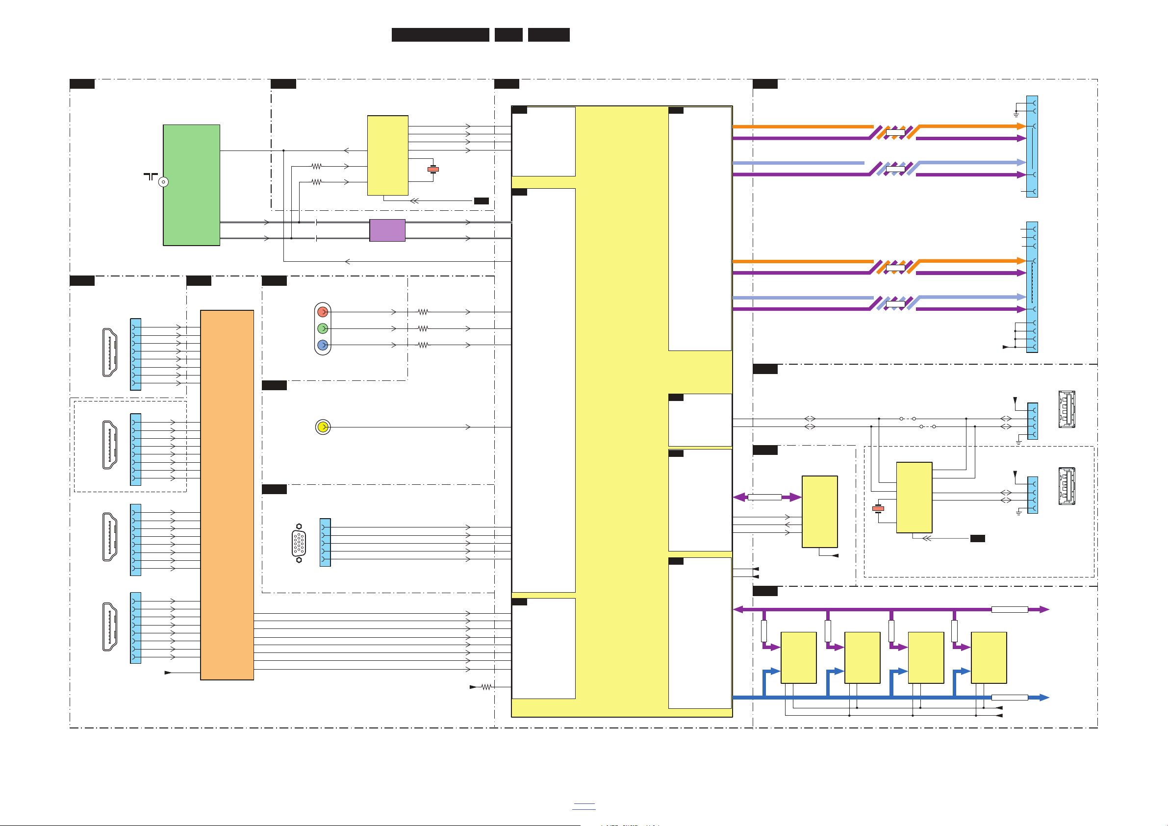
EN 68Q552.2L LA 9.
Block Diagrams
2011-Jul-15
back to
div. table
Block Diagram Video
B02
PNX85500
B06B
VIDEO OUT - LVDS
B04A
ANALOGUE EXTERNALS A
B01I
VGA
B04B
ANALOGUE EXTERNALS B
B01K
TUNER BRASIL
B01F
TUNER
B05A
DDR
B01C
USB HUB
B01B
FLASH
B01H
HDMI
B04D
HDMI
1E01
1E08
7S00
PNX85537EB
VIDEO STREAM
B02A
LVD S
B02F
ANALOG VIDEO
B02I
HDMI_DV
B02C
AV2-CVBS
VIDEO
YPBPR
1
1E05
2
3
14
13
R-VGA
G-VGA
B-VGA
H-SYNC-VGA
V-SYNC-VGA
1
6
10
11
5
15
VGA
CONNECTOR
AB14
AC18
AB18
AE16
AD16
AF16
63
HDMIA-RXC-
HDMIA-RX0+
HDMIA-RX0-
HDMIA-RX1+
HDMIA-RX1-
HDMIA-RX2+
HDMIA-RX2-
62
61
60
59
58
57
56
HDMIA-RXC+
U26
T25
T26
W24
U25
V26
W26
W25
V25
RREF
PNX85537
19110_005_110309.eps
110321
VIDEO
2
TUNER_P
TUNER_N
IF_AGC
VGA_R
VSYNC_IN
VGA_G
VGA_B
CVBS-_Y2
AC15
YPBPR1-PR
PR_R_C1
AD15
YPBPR1-PB
PB_B1
AE15
YPBPR1-SYNCIN1
AV3-PR
AV3-PB
AV3 -Y
Y_G1
TNR_SER1_MIVAL
TNR_SER1_SOP
TNR_SER1_MICLK
TNR_SER1_DATA
HSYNC_IN
+3V3
3S0W
PX1
PX2
PX3
PX4
TO DISPLAY
TO DISPLAY
1G51
+VDISP
I2C
N.C.
50
51
49
40
40
3
4
2
1
1G50
N.C.
1
2
3
3
41
MEMORY
B02B
V1
DDR2-VREF-CTRL3
A2
DDR2-VREF-CTRL2
VREF_2
VREF_1
CONROL
B02E
FLASH
B02A
USB-DM
USB-DP
R26
R25
USB_DP
USB_DN
LOUT1
LOUT2
LOUT3
LOUT4
*7EC1
SII9187BC
SII9287BC
HDMI
SWITCH
VCC33
RXC
RXD
RXB
RXA
18
17
16
15
14
13
12
11
8
7
6
5
4
3
2
1
72
71
70
69
68
67
66
65
26
25
24
23
22
21
20
19
19
1
18 2
1
1P05
3
4
7
9
10
12
6
DRX2+
DRX2-
DRX1+
DRX1-
DRX0+
DRX0-
DRXC+
DRXC-
HDMI SIDE
CONNECTOR
19
1
18 2
1
1P02
3
4
7
9
10
12
6
CRX2+
CRX2-
CRX1+
CRX1-
CRX0+
CRX0-
CRXC+
CRXC-
HDMI 1
CONNECTOR
1
1P03
3
4
7
9
10
12
6
BRX2+
BRX2-
BRX1+
BRX1-
BRX0+
BRX0-
BRXC+
BRXC-
1
1P04
3
4
7
9
10
12
6
ARX2+
ARX2-
ARX1+
ARX1-
ARX0+
ARX0-
ARXC+
ARXC-
19
1
18 2
HDMI 2
CONNECTOR
19
1
18 2
HDMI 3
CONNECTOR
9,27,64
+3V3-HDMI
3E90
3E89
3E87
DDR2-VREF-DDR
A1 E2A1 E2A1 E2A1 E2
+1V8
SDRAM
128Mx8
7B01
H5PS1G83E
SDRAM
128Mx8
7B02
H5PS1G83E
SDRAM
128Mx8
7B03
H5PS1G83E
DQ
A
SDRAM
128Mx8
7B00
H5PS1G83E
VREF
VDDL
VREF
VDDL
VREF
VDDL
VREF
VDDL
DDR2-D(0-31)
D(24-31)
D(16-23)
D(8-15)
D(0-7)
DDR2-A(0-14)
TXC_N
TXC_P
TX0_N
TX0_P
TX1_N
TX1_P
TX2_N
TX2_P
RX1_A_N
RX0_A_P
RX0_A_N
RX1_A_P
RX2_A_N
RXC_A_N
RXC_A_P
RX2_A_P
4321
USB1-DM
USB1-DP
USB2-DM
USB2-DP
SIDE USB
CONNECTOR
1P08
+5V-USB2
+5V-USB1
17
21
22
18
9
10
13
14
2
1
3
4
4321
SIDE USB
CONNECTOR
1P07
2
1
3
4
9F26
9F25
7FL5
CY7C65631
USB
HUB
1FL5
24M
ONLY FOR 8000 SERIE
*6000/7000 SERIE MUX SII9187 NON INSTAPORT
8000 SERIE MUX SII9287 INSTAPORT
OPTIONAL
29
30
58
59
61
60
AD12
AE12
R23
T22
R22
T21
AF12
PNX-IF-AGC
2F75
2F79
1T01
FA2327
IF-OUT1
IF-OUT2
MAIN HYBRID
TUNER
9
PNX-IF-P
PNX-IF-N
11
10
4MHZ_REF
9
RF IN
BANDPASS
FILTER
TUN-IF-P
TUN-IF-N
7FE0
TC90517FG
DEMODULATOR
(ISDB-T)
TS-FE-VALID
RESET-SYSTEMn
IF-
IF AGC
IF+
TS-FE-SOP
TS-FE-CLOCK
TS-FE-DATA
3F80
3F81
B02E
42
1FE0
25M4
19
18
NAND-CE1n
7F20
H27U4G8F2DTR-BC
NAND
FLASH
E21
21,37
+3V3
VCC
XIO_D
NAND_CE1
NAND_RDY1
NAND_WP_
XIO-D(00-07)
NAND-RDY1n
F21
NAND-WPn
A21
9
7
19
RESET-USBn
B02G
42
Page 69
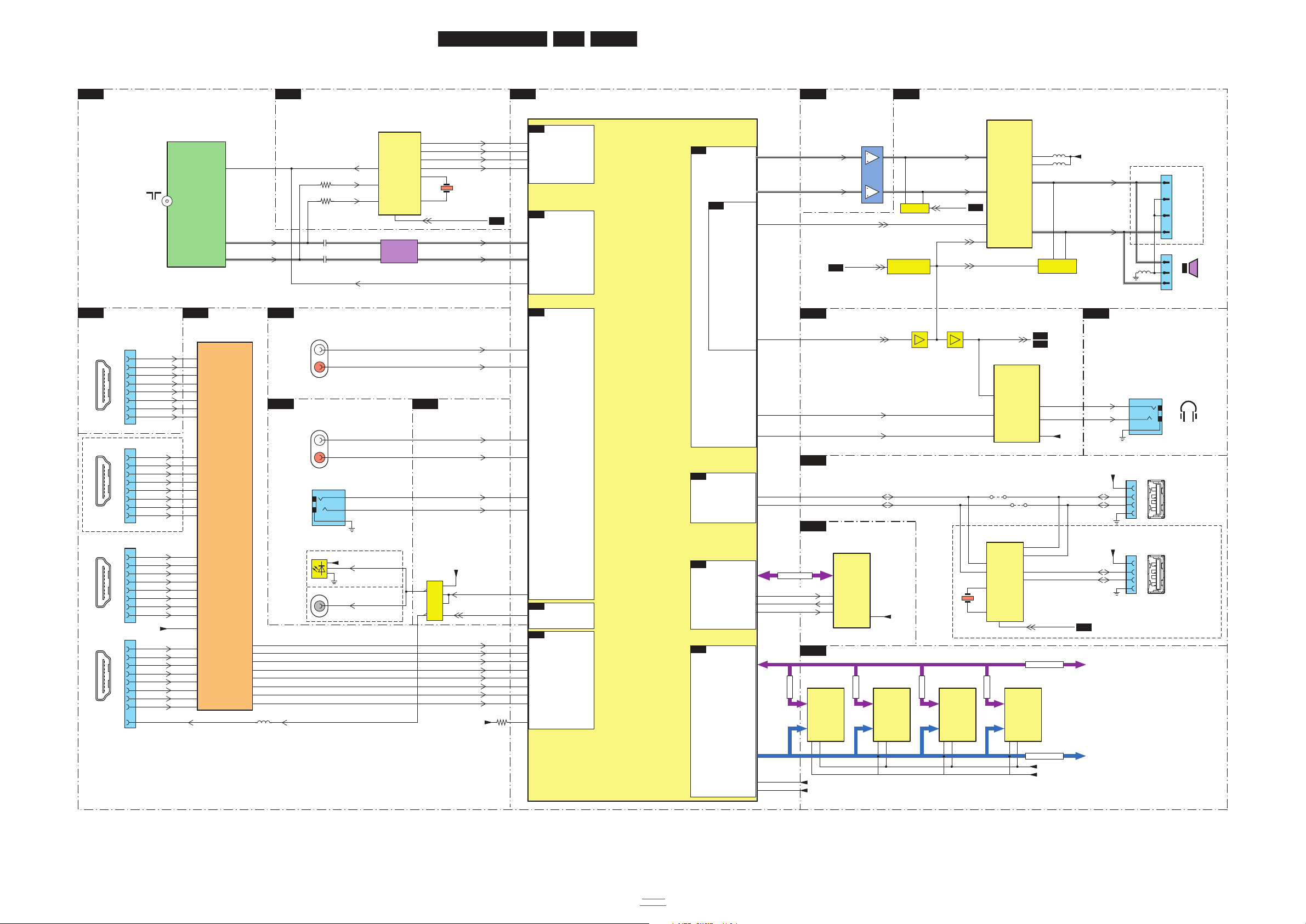
Block Diagrams
EN 69Q552.2L LA 9.
2011-Jul-15
back to
div. table
9-4 Block Diagram Audio
B01H
HDMI
B04D
HDMI
B02D
PNX85500: AUDIO
B02D
PNX85500: AUDIO
B03A
AUDIO
B04E
HEADPHONE
B04B
ANALOGUE EXTERNALS B
B04A
ANALOGUE EXTERNALS A
B01J
TEMP SENSOR + HEADPHONE
B02
PNX85500
B05A
DDR
B01C
USB HUB
B01B
FLASH
B01K
TUNER BRASIL
B01F
TUNER
7S00
PNX85537EB
AUDI O
B02D
STANDBY
B02G
HDMI_DV
B02C
STANDBY
B02G
PNX85537
19110_006_110309.eps
110321
NAND-CE1n
AE10
AF10
1E08
4
6
1E02
2
4
AUDIO-IN3-L
AUDIO-IN3-R
AE9
AF9
AUDIO IN
L+R
AUDIO IN
L+R
ADAC_2
PO_7
PO_6
ADAC3
ADAC4
ADAC_1
AUDIO
AUDIO-IN1-L
AUDIO-IN1-R
*7EC1
SII9187BCNU
SII9287BCNU
HDMI
SWITCH
VCC33
RXC
RXD
RXB
RXA
19
1
18 2
1
1P05
3
4
7
9
10
12
6
DRX2+
DRX2-
DRX1+
DRX1-
DRX0+
DRX0-
DRXC+
DRXC-
HDMI SIDE
CONNECTOR
19
1
18 2
1
1P02
3
4
7
9
10
12
6
CRX2+
CRX2-
CRX1+
CRX1-
CRX0+
CRX0-
CRXC+
CRXC-
HDMI 1
CONNECTOR
1
1P03
3
4
7
9
10
12
6
BRX2+
BRX2-
BRX1+
BRX1-
BRX0+
BRX0-
BRXC+
BRXC-
1
1P04
3
4
7
9
10
12
6
ARX2+
ARX2-
ARX1+
ARX1-
ARX0+
ARX0-
ARXC+
ARXC-
19
1
18 2
HDMI 2
CONNECTOR
19
1
18 2
HDMI 3
CONNECTOR
14
ARC-eHDMI+ eHDMI+
9,27,64
+3V3-HDMI
AD9
AC9
AUDIO-IN4-L
AUDIO-IN4-R
VGA
AUDI O
1E09
2
3
1
AIN4_L
AIN4_R
AIN1_R
AIN3_L
AIN3_R
AIN1_L
VIDEO STREAM
B02A
ANALOG VIDEO
B02I
AUDIO
B02D
TUNER_P
TUNER_N
IF_AGC
TNR_SER1_MIVAL
TNR_SER1_SOP
TNR_SER1_MICLK
TNR_SER1_DATA
MEMORY
B02B
V1
DDR2-VREF-CTRL3
A2
DDR2-VREF-CTRL2
VREF_2
VREF_1
1E07
1
AF5
AF18
DIGITAL
AUDIO
OUT
SPDIF-OUT-PNX
SEL-HDMI-ARC
SPDIF-OUT
SPDIF-OPT
2
1
4
5
3
8
SPDIF_OUT
P0_4
7S09
74LVC00
&
+3V3
CONROL
B02E
FLASH
B02A
7F20
H27U4G8F2DTR-BC
NAND
FLASH
R26
R25
E21
21,37
+3V3
VCC
USB_DP
USB_DN
XIO_D
NAND_CE1
NAND_RDY1
NAND_WP_
XIO-D(00-07)
5EC2
63
HDMIA-RXC-
HDMIA-RX0+
HDMIA-RX0-
HDMIA-RX1+
HDMIA-RX1-
HDMIA-RX2+
HDMIA-RX2-
62
61
60
59
58
57
56
HDMIA-RXC+
U26
T25
T26
W24
U25
V26
W26
W25
V25
RREF
+3V3
3S0W
TXC_N
TXC_P
TX0_N
TX0_P
TX1_N
TX1_P
TX2_N
TX2_P
RX1_A_N
RX0_A_P
RX0_A_N
RX1_A_P
RX2_A_N
RXC_A_N
RXC_A_P
RX2_A_P
DDR2-VREF-DDR
A1 E2A1 E2A1 E2A1 E2
+1V8
SDRAM
128Mx8
7B01
H5PS1G83EFR
SDRAM
128Mx8
7B02
H5PS1G83EFR
SDRAM
128Mx8
7B03
H5PS1G83EFR
DQ
A
SDRAM
128Mx8
7B00
H5PS1G83EFR
VREF
VDDL
VREF
VDDL
VREF
VDDL
VREF
VDDL
DDR2-D(0-31)
D(24-31)
D(16-23)
D(8-15)
D(0-7)
DDR2-A(0-14)
29
30
58
59
61
60
AD12
AE12
R23
T22
R22
T21
AF12
PNX-IF-AGC
2F75
2F79
1T01
FA2327
IF-OUT1
IF-OUT2
MAIN HYBRID
TUNER
9
PNX-IF-P
PNX-IF-N
11
10
4MHZ_REF
9
RF IN
BANDPASS
FILTER
TUN-IF-P
TUN-IF-N
7FE0
TC90517FG
DEMODULATOR
(ISDB-T)
TS-FE-VALID
RESET-SYSTEMn
IF-
IF AGC
IF+
TS-FE-SOP
TS-FE-CLOCK
TS-FE-DATA
1E10
8000 SERIES
6000/7000 SERIES
+3V3
1
2
3
USB-DM
USB-DP
4321
USB1-DM
USB1-DP
USB2-DM
USB2-DP
USB 1 SIDE
CONNECTOR
1P08
+5V-USB2
+5V-USB1
17
21
22
18
9
10
13
14
2
1
3
4
4321
USB 2 SIDE
CONNECTOR
1P07
2
1
3
4
9F26
9F25
7FL5
CY7C65631
USB
HUB
1FL5
24M
ONLY FOR 8000 SERIE
*6000/7000 SERIE MUX SII9187 NON INSTAPORT
8000 SERIE MUX SII9287 INSTAPORT
18
17
16
15
14
13
12
11
8
7
6
5
4
3
2
1
72
71
70
69
68
67
66
65
26
25
24
23
22
21
20
19
OPTIONAL
3F80
3F81
B02E
42
1FE0
25M4
19
18
NAND-RDY1n
F21
NAND-WPn
A21
9
7
19
RESET-USBn
B02G
42
AD7
AE7
1735
1
2
3
4
SPEAKERS
RES
ADAC(1)
ADAC(2)
+AUDIO-L
-AUDIO-R
RESET-AUDIO
AB19
AC19
ADAC(4)
AMP1
AMP2
ADAC(3)
HEADPHONE
OUT 3.5mm
AF7
AD6
7EE1
TPA6111A2DGN
HEADPHONE
AMPLIFIER
1
7
IN-1
SHUTDOWN
IN-2
2
6
5
A-PLOP
B03A
B03C
7D10
TPA3123D2PWP
CLASS D
POWER
AMPLIFIER
OUT-L
PVCC_L
PVCC_R
OUT-R
512
10
6
22
15
IN-R
IN-L
MUTE
SD
4
2
AUDIO-MUTE-UP
A-STBY
A-STBY
B04A
STANDBY &
PROTECTION
7D03
MAINS SWITCH
DETECT
7D11
LEFT-SPEAKER
RIGHT-SPEAKER
1328
2
3
1
7EE0-1 7EE0-2
1D38
1
2
3
DETECT2
5D03
8
+3V3
1,3
10,12
+24V-AUDIO-POWER
5D07
5D08
VDD
VO_1
VO_2
7S05
LM324P
14
8
A-PLOP
7D15
A-PLOP
B04E
Page 70
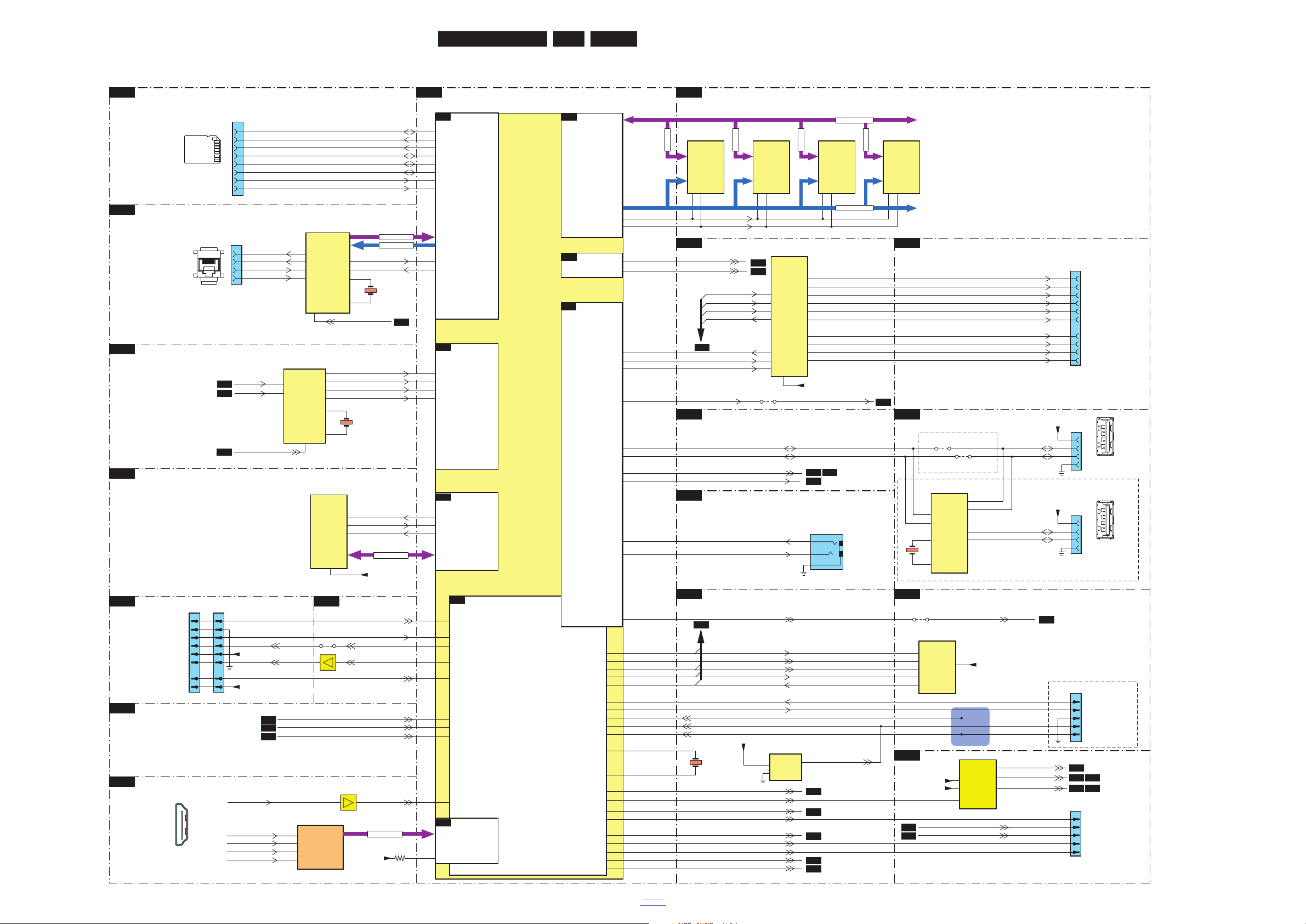
EN 70Q552.2L LA 9.
Block Diagrams
2011-Jul-15
back to
div. table
9-5 Block Diagram Control & Clock Signals
B01D
SD-CARD
B02A
PNX85500
B06C
AMBILIGHT CPLD
B04C
ETHERNET + SERVICE
B09A
CONNECTORS COMP
B01B
FLASH
B03C
DC / DC
B05A
DDR
B01E
PNX85500-CONTROL
B04C
ETHERNET + SERVICE
B02E
PNX85500: MIPS
B01C
USB HUB
B03C
DC / DC
B02G
PNX85500: STANDBY CONTROLLER
B02G
PNX85500: STANDBY CONTROLLER
B04D
HDMI
CONTROL + CLOCK SIGNALS
B09A
NON DVBS CONNECTOR BOARD
B1K
TUNER BRASIL
RES
VIDEO STREAM
B02A
B02E
ETHERNET
1M95
11
10
9
LED1
AD26
AE26
AA22
DETECT2
AA26
AF19
RESET-STBYn
4x HDMI
CONNECTOR
AB22
RESET-SYSTEMn
AD21
ENABLE-3V3n
PNX85537
7S00
PNX85537EB
SD-CARD
CONNECTOR
AC25
LED2
1S02
54M
AF17
AE17
CONTROL
B02E
STANDBY
B02G
HDMI_DV
B02C
AF20
STANDBY
AD19
AD23
KEYBOARD
RC
LIGHT-SENSOR
AD18
AC19
RESET-USBn
AB19
RESET-AUDIO
AF1
SENSE+1V1
BACKLIGHT-PWM_BL-VS
BACKLIGHT-BOOST
B01C
AC21
POWER-OK
B01F
B02E
B01F
B03B
B06C
B01E
7S20
NCP303LSN28G
2
INP
1
OUTP
+3V3-STANDBY
GND
B02E
B02H
POWER
7EC1
SII9187BCNU
SII9287BCNU
HDMI
SWITCH
P3_0
P3_1
P1_7
P6_4
P2_2
P2_7
P1_1
P2_6
P0_6
P2_3
VDD_1V1
XTAL_IN
XTAL_OUT
P5_1
P5_0
P3_2
P3_3
RESET_IN
P1_2
W24
RREF
RX
P1_0
PWM_1
PWM_0
TO
POWER SUPPLY
+3V3-STANDBY
+5V
B04E
B03C
SDM
SPI-PROG
AF22
AB20
FF04
FF29
19110_007_110318.eps
110321
RXD-UP
TXD-UP
Y23
Y24
UART
SERVICE
CONNECTOR
AE21
AF21
RXD1-MIPS
TXD1-MIPS
LED-2
LED-1
1
2
3
4
5
6
7
8
1M19
1
4
7
3
6
2
5
8
*1M20
7U43
ARX-HOTPLUG
1E06
2
3
1
P2_0
AC20
LCD-PWR-ONn
B03H
RESET-STBYn
AUDIO-MUTE-UP
B03A
P0_7
AA15
N5
N4
SENSE+1V2
B03D
VDDA_1V2
AE18
RESET-ETHERNETn
B04C
P0_3
AF18
SEL-HDMI-ARC
B02D
P0_4
AE20
LAMP-ON
V23
BOOST-PWM
GPIO_10
B03C
BACKLIGHT-BOOST
12
2
31
BRX-HOTPLUG
CRX-HOTPLUG
41
DRX-HOTPLUG
45
35
PCEC-HDMI
CEC-HDMI
1
2
19
18
1P05-19
1P02-19
1P03-19
1P04-19
TO PIN:
1P02-13
1P03-13
1P04-13
1P05-13
FLASH
B02A
7F20
H27U4G8F2DTR
NAND
FLASH
12,37
+3V3
VCC
1P09
W2
1
SDIO-DAT3
CC_DAT3
2
W6
SDIO-CLK
SDIO-CMD
CMD
AA2
ETH-TXCLK
RXCLK
10
U6
SDIO-CDn
SDCD
AA3
ETH-RXCLK
TXCLK
12
V6
SDIO-WP
SDWP
RXD
TXD
W1
5
CLK
7
W5
SDIO-DAT0
DAT_0
8
W4
SDIO-DAT1
DAT_1
9
W3
SDIO-DAT2
DAT_2
DDR-CLK_N
DDR-CLK_P
3
SPI_CLK
SPI_CSB
SPI_SDO
SPI_SDI
P6_5
7F52
M25P05-AVMN6P
FLASH
512K
8
+3V3-STANDBY
VCC
6
PNX-SPI-CLK
AF24
3
PNX-SPI-WPn
AE22
1
PNX-SPI-CSBn
AF23
5
PNX-SPI-SDO
AE23
2
PNX-SPI-SDI
AF25
CONTROL
+3V3-STANDBY
+12V
ENABLE-1V8
ENABLE-3V3-5V
DETECT2
XIO-D(00-07)
ETH-TXD
ETH-RXD
XIO_D
MEMORY
B02B
F8 E8F8 E8F8 E8F8 E8
SDRAM
128Mx8
7B01
H5PS1G83EFR
SDRAM
128Mx8
7B02
H5PS1G83EFR
SDRAM
128Mx8
7B03
H5PS1G83EFR
DQ
A
CLK_N
CLK_P
GPI0_2
V22
GPI0_7
GPI0_3
SDRAM
128Mx8
7B00
H5PS1G83EFR
DDR2-D(0-31)
D(24-31)
D(16-23)
D(8-15)
D(0-7)
DDR2-A(0-13)
B06C
BL_PWM
BACKLIGHT-PWM
AD5
BACKLIGHT-PWM_BL-VS
RESET-SYSTEMn
AE4
B01K B02G
RESET_SYS
GPI0_11
SELECT-SAW
U23
B01F
CLK_54_OUT
AC5
PXCLK54
B02G
+3V3
3S0W
TO IR / LED BOARD AND
KEYBOARD CONTROL
9U41
9CH0
B03E
B03B B03D
B02G B03A
EF
7EC0
T21
T22
7
20
R22
R23
B02G
RESET-ETHERNETn
19
29
28
31
30
1M59
3
1
4
6
9
8
12
11
13
14
Pin8 Pin3Pin5Pin7 Pin6 Pin4
Pin9
Pin2 Pin1
7GA0
XC9572XL
CPLD
26
VIO
VCCIO
41
43
GPIO_1
Y22
7
40
PNX-SPI-SDI
39
PNX-SPI-SDO
3
PNX-SPI-CS-BLn
PNX-SPI-CLK
3D-LR
AMBI-SPI-CLK-OUT
AMBI-SPI-SDO-OUT
27
22
AMBI-SPI-SDI-OUT_G1
23
AMBI-PWM-CLK_B2
29
AMBI-SPI-CS-OUTn_R2
30
AMBI-LATCH1_G2
31
AMBI-PROG_B1
19
AMBI-BLANK_R1
20
AMBI-LATCH2_DIS
28
AMBI-TEMP
32
5
PNX-SPI-CSBn
HDMIA-RX
4321
USB-DM1
USB-DP1
USB-DM2
USB-DP2
SIDE USB
CONNECTOR
1P08
+5V-USB2
+5V-U
SB1
17
21
22
18
9
10
2
1
3
4
4321
SIDE USB
CONNECTOR
1P07
2
1
3
13
14
4
9F26
9F25
7FL5
CY7C65631
USB
HUB
USB-DM
USB-DP
R26
R25
USB_DP
USB_DN
TNR_SER1_MIVAL
TNR_SER1_SOP
TNR_SER1_MICLK
TNR_SER1_DATA
1F51
1
3
4
5
2
LEVEL SHIFTED
FOR
DEBUG USE
ONLY
7E10
LAN8710A-EZK
ETHERNET
ETHERNET
CONNECTOR
RJ45
TO AMBILIGHT
MODULE
SDM
SPI-PROG
1FL5
24M
1E70
25M
4
5
7FJ0
CXD2820R
DEMODULATOR
(ISDB-T)
IF+
IF-
4
3
30
29
5
7
TS-FE-VALID
TS-FE-SOP
TS-FE-CLOCK
TS-FE-DATA
ONLY FOR 8000 SERIE
ONLY FOR 6000/7000 SERIE
OPTIONAL
9GA0
B03C
RESET-SYSTEMn
NAND-CE1n
E21
NAND_CE1
NAND_RDY1
NAND_WP_
NAND-RDY1n
F21
NAND-WPn
A21
9
7
19
1FE0
25M4
18
19
1N00
1
ETH-TXP
2
ETH-RXP
ETH-TXN
3
6
ETH-RXN
SUNDANCE / INFINITY
Page 71
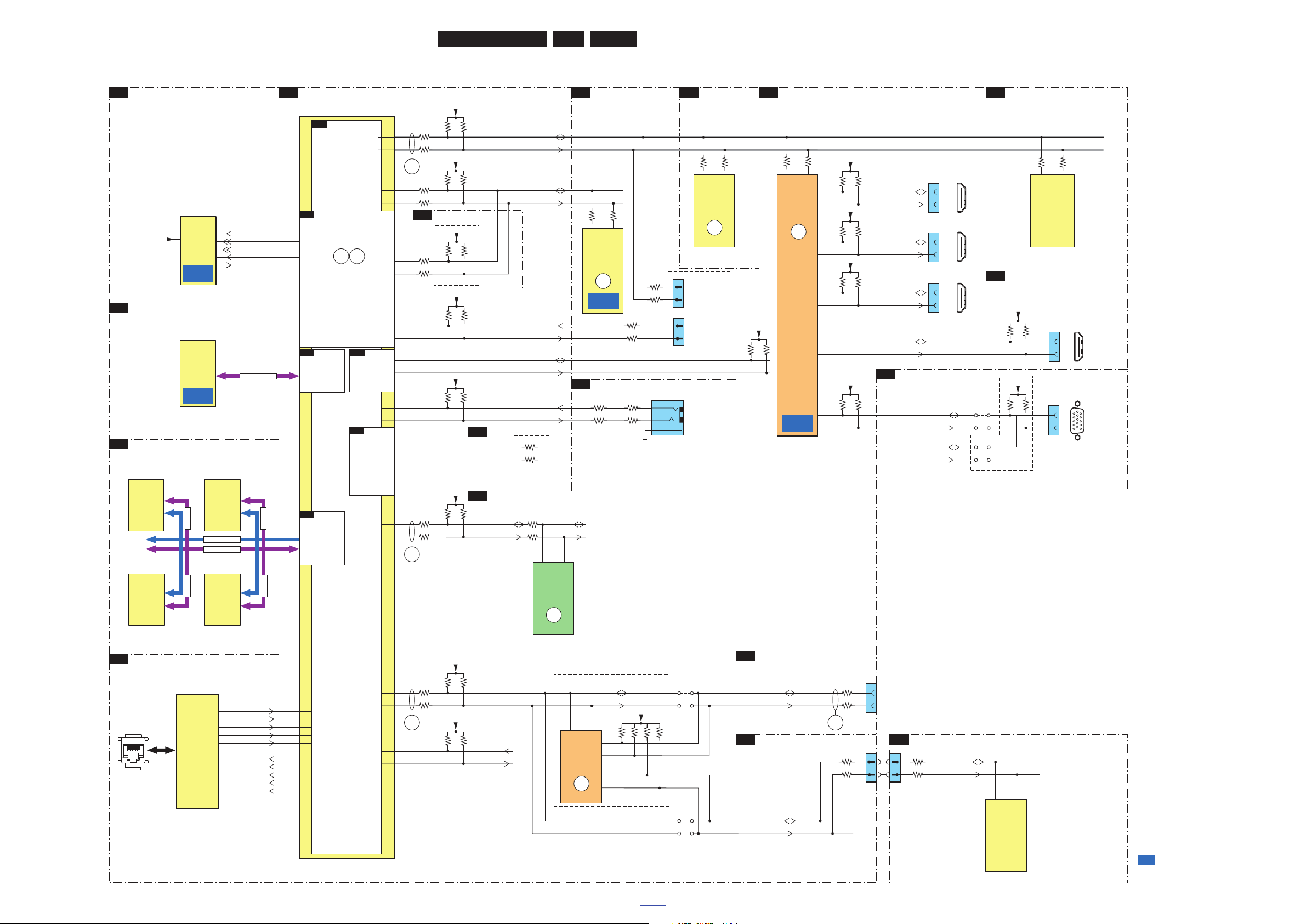
Block Diagrams
EN 71Q552.2L LA 9.
2011-Jul-15
back to
div. table
9-6 Block Diagram I2C
I²C
PNX85500: MIPS
B02E
DDR
B05A
FLASH
B01B
ETHERNET + SERVICE
B04C
PNX85500: CONTROL
B01E
PNX85500-CONTROL
B01E
PNX85500: STANDBY
CONTROLER
B02G
HDMI
B04D
HDMI
B01H
TEMP SENSOR +
HEADPHONE
B01J
TUNER BRAZIL
B01K
TUNER
B01F
PNX85500: ANALOG VIDEO
B02I
ETHERNET + SERVICE
B04C
VGA
B01I
VIDEO OUT - LVDS
B06B
DVBS CONNECTOR BOARD
B09A
TEMP SENSOR
TS1
1F52
7S00
PNX85537EB
PNX85537
SDA-SSB
SCL-SSB
C25
C26
1_SDA
1_SCL
AC23
AC24
MC_SDA
MC_SCL
B25
A24
3_SDA
3_SCL
SDA-UP-MIPS
SCL-UP-MIPS
CONTROL
STANDBY
1
3
DEBUG
ONLY
19110_004_110309.eps
110321
RES
3F63
3F62
56
7F58
M24C64
EEPROM
(NVM)
3F60
3F59
TUN-P7
TUN-P6
SDA-TUNER
SCL-TUNER
76
1T01
TH2627
MAIN
TUNER
3S60
3S61
3F75
3F76
53 54
7EC1
SII9287B
SII9187A
HDMI
MUX
3EC5
3EC3
HDMI
CONNECTOR 3
HDMI
CONNECTOR 2
1P04
16
15
29
30
1P03
16
15
33
34
1P02
16
15
39
40
HDMI
CONNECTOR
SIDE
1P05
16
15
3FBF-2
3FBF-1
DIN-5V
43
44
47
48
Y25
Y26
Y23
Y24
GPIO_2
GPIO_3
DDCA-SDA
DDCA-SCL
ARX-DDC-SDA
ARX-DDC-SCL
BRX-DDC-SDA
BRX-DDC-SCL
CRX-DDC-SDA
CRX-DDC-SCL
DRX-DDC-SDA
DRX-DDC-SCL
12
7FD1
LM75BDP
TEMP
SENSOR
3FD3
3FD4
46 45
7FE0
TC90517FG
DEMODULATOR
3FE9
3FE8
3S56
3S57
3S2F
3S2G
3S5Y
3S5Z
3S6D
3S6E
+3V3
3S69
3S6A
+3V3
3S6V
3S6W
+3V3-STANDBY
3S81
3S80
+3V3
3S83
3S84
+3V3
3S6F
3S6G
+3V3
AD25
AD24
1E05
12
15
VGA-SDA-EDID-HDMI
VGA-SCL-EDID-HDMI
VGA-SDA-EDID
VGA-SCL-EDID
3FC1
3FC2
+5V-VGA
9FC2
9FC4
9FC1
9FC3
RES
RES
3S5V-1
3S5V-3
3EC1-1
3EC1-3
AIN-5V
3ECA-1
3ECA-2
BIN-5V
3ECA-3
3ECA-4
CIN-5V
3ECP-3
3ECP-1
+5V-EDID
3ECU-2
3ECU-4
+3V3
B24
Y5
Y6
AB4
AC1
AA3
11
10
9
8
7
A23
4_SDA
4_SCL
AE21
AF21
P3_0
P3_1
1
6
10
11
5
15
VGA
CONNECTOR
RXD1-MIPS
TXD1-MIPS
W21
W22
GPIO_2
GPIO_3
RXD2-MIPS
TXD2-MIPS
UART
SERVICE
CONNECTOR
1E06
3
2
1
3E53-3
3E53-1
3E53-4
3E53-2
1F51
1
3
B02E
B02G
MEMORY
B02B
FLASH
B02A
ANALOGUE
VIDEO
VGA_EDID_SDA
VGA_EDID_SCL
B02I
B02C
ERR
35
ERR15ERR
53
4
5
SDA-BL
SCL-BL
SDA-TEMP1
SCL-TEMP1
LVD S
CONNECTOR
Programmable via USB
1G51
50
49
SDA-DISP
SCL-DISP
3C83
3C81
3S67
3S65
3S68
3S66
+3V3
B26
A25
2_SDA
2_SCL
SDA-SET
SCL-SET
3S58
3S5W
3S6B
3S6C
+3V3
3S1G
3S1H
+3V3-STANDBY
RES
7
8
9S13
9S10
3G2W
3G2Y
uP
LEVEL SHIFTED
FOR DEBUG
USE ONLY
RXD-UP
TXD-UP
3F65
3F64
21
7S01
PCA9540B
2 CHAN.
MULTIPLEX.
ERR
24
ERR
34
ERR
23
ERR
42
12
7104
LM75ADP
TEMP
SENSOR
9S12
9S11
7E10
LAN8710A-EZK
ETH-RXD(0)
ETH-RXD(3)
ETH-RXCLK
ETH-RXD(1)
ETH-RXD(2)
AA1
AA4
AB1
AB2
AA2
22
23
24
25
20
ETH-TXD(0)
ETH-TXD(3)
ETH-TXCLK
ETH-TXD(1)
ETH-TXD(2)
RXD_0
RXD_1
RXD_2
RXD_3
RXCLK
TXD_0
TXD_1
TXD_2
TXD_3
TXCLK
XIO_D
DQ
A
ETHERNET
DDC_A_SDA
DDC_A_SCL
HDMI_DV
HDMI
CONNECTOR 1
ETHERNET
CONNECTOR
RJ45
RES
SDRAM
128Mx8
7B01
H5PS1G83EFR
SDRAM
128Mx8
7B02
H5PS1G83EFR
FLASH
(4Gx16)
SDRAM
128Mx8
7B03
H5PS1G83EFR
SDRAM
128Mx8
7B00
H5PS1G83EFR
DDR2-D(0-31)
XIO-D(00-07)
D(24-31)
D(16-23)
D(8-15)
D(0-7)
DDR2-A(0-13)
19
1
18 2
19
1
18 2
19
1
18 2
19
1
18 2
SPI_CLK
SPI_CSB
SPI_SDO
SPI_SDI
P6_5
7F52
M25P05-AVMN6P
FLASH
512K
8
+3V3-STANDBY
VCC
6
PNX-SPI-CLK
AF24
3
PNX-SPI-WPn
AE22
1
PNX-SPI-CSBn
AF23
5
PNX-SPI-SDO
AE23
2
PNX-SPI-SDI
AF25
7F20
H27U4G8F2DTR
ERR
13
ERR
18
ERR
14
ERR
64
STANDBY
SW
MAIN
SW
MAIN NVM
SW
EDID
SW
SW
RES
1M71 1T02
33
11
3124
3123
OPTIONAL
Page 72
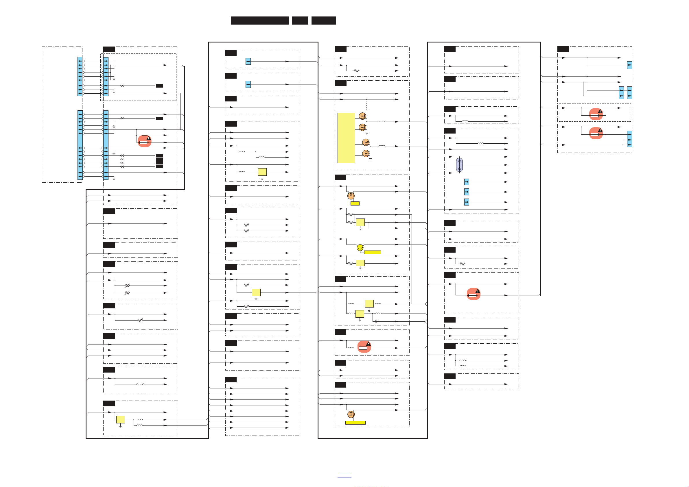
EN 72Q552.2L LA 9.
Block Diagrams
2011-Jul-15
back to
div. table
9-7 Supply Lines Overview
B01A
COMMON INTERFACE
B01D
SD-CARD
B01F
TUNER
B01K
TUNER BRAZIL
B01C
USB HUB
B02B
PNX85500: SDRAM
B01B
FLASH
B02A
PNX85500: NANDFLASH
CONDITIONAL ACCESS
B02C
PNX85500: DIGITAL VIDEO IN
B02E
PNX85500: MIPS
B02G
PNX85500: STANDBY CONTROLLER
B02H
PNX85500: POWER
B01H
HDMI
B01I
VGA
B01J
TEMP SENSOR + HEADPHONE
B01E
PNX85500: CONTROL
B03D
DC / DC
B03E
DC / DC
B09A
CONNECTORS COMP
B04A
ANALOGUE EXTERNALS A
B04C
ETHERNET + SERVICE
B03F
TEMPSENSOR + AMBILIGHT
B06A
DISPLAY INTERFACING-VDISP
B02D
PNX85500: AUDIO
B03A
AUDI O
B03B
DC / DC
SUPPLY LINES OVERVIEW
PSU
B03C
DC / DC
B03H
VDISP - SWITCH
B04D
HDMI
B04E
HEADPHONE
B04B
ANALOGUE EXTERNALS B
B06B
VIDEO OUT - LVDS
B06D
SPI-BUFFER
B06C
AMBILIGHT CPLD
B05A
DDR
B01G
TOSHIBA SUPPLY
B03G
FAN - CONTROL
+3V3
+3V3
B03e
B03e
B03e
+3V3-SD
3F40
+T
+3V3
+3V3
+5V-TUN-PIN
+5V-TUN
+5V-TUN
B03e
+5V
+5V
+5V-USB2
3FL2
+T
+5V-USB1
3F32
+T
B03e
+3V3
+3V3
B03e
+1V8
+1V8
DDR2-VREF-CTRL2
DDR2-VREF-CTRL3
B03c
+3V3
+3V3
+3V3
+3V3
+5V
+5V
B03e
+3V3
+3V3
B03e
B03e
B01g
B03e
B03b
+3V3
+3V3
B03e
B03b,d,e,g,
B09a
B01e,B02e,
g,h,B03a,b,h,
B04d,e,B09a
B02d,B03a
+3V3
+3V3
B03e
+3V3-STANDBY
+3V3-STANDBY
B03c
+1V1
+1V1
B03b
+3V3-STANDBY
+3V3-STANDBY
B03c
+1V1
+1V1
B03b
+1V2
+1V2
B03d
+1V8
+1V8
B03b
+2V5
+2V5
B03d
+2V5-AUDIO
+2V5-AUDIO
B02d
+2V5-LVDS
+2V5-LVDS
B03d
+3V3
+3V3
B03e
+3V3-STANDBY
+3V3-STANDBY
B03
c
DIN-5V
+3V3
+3V3
+1V2-BRA-VDDC
+1V2-BRA-VDDC
+1V2-BRA-DR1
+1V2-BRA-DR1
+3V3
+3V3
B03e
+3V3-STANDBY
+3V3-STANDBY
B03c
+5V
+5V
B03e
B03d
B03e
9F71
+3V3-BRA
+3V3
+3V3
5FE7
+3V3
+5V+5V
+2V5-LVDS
+2V5
B03e
+2V5-AUDIO
+3V3-ARC
+3V3+3V3
B03d
+2V5+2V5
+2V5-BRA
+3V3-BRA-FLT
+5V+5V
7FE3
IN OUT
COM
5FE9
5FE4
3S20
3S06
+24V-AUDIO-POWER
+24V-AUDIO-POWER
+24V-AUDIO-VDD
3S0Z
3S11
B03c
B03c
+3V3-STANDBY+3V3-STANDBY
+24V-AUDIO-POWER
+24V-AUDIO-POWER
+AVCC
3D09
7U03
TPS53126PW
+12V
+1V8
12
14
+1V1
5U01
23
+12V
12V/1V1
COVERSION
12V/1V8
COVERSION
5U02
5U00
B03c
+3V3-STANDBY
+3V3-STANDBY
B03c
Dual
Synchronous
Step-Down
Controller
7U04
7U01
7U02-2
7U02-1
1
1M95
11
66
77
88
1M95
+3V3-STANDBY
+12V_AL
3V3SB
+12V3
1M99
11
66
77
22
33
44
88
55
LAMP-ON
14 14
1M99
BACKLIGHT-BOOST
GND_AL
B03h
B09a
B09a
+12VIN
BACKLIGHT-PWM_BL-VS
+12V
99
+24V-AUDIO-POWER
13 13
+24V
10 10
+VSND
BL-DIM1
BL-I-CTRL
POK
99
22
33
44
55
STANDBY
STANDBY
GND1
GND1
GND1
BL-ON-OFF
+12V3
11 11
+24V
GND1
1U40
T 3.0A
+12VIN
+12VD
CUA0
+1V2
+1V8+1V8
+12V
7UA3
B03b
+3V3-ET-ANA
+3V3+3V3
B03e
B03e
+2V5-REF
+12V+12V
B03c
B03b
B02h
B03c
B03e
B03e
3U16
3UA0
7UC0
IN OUT
COM
3U15
7UA0
VOLT.
REG.
+5V-TUN
+5V5-TUN+5V5-TUN
7UA6
ENABLE-1V8
+3V3
+12V+12V
+1V1+1V1
+3V3+3V3
B03e
+3V3+3V3
5UD3 5UD2
+5V
+5V5-TUN
6UD0
7UD1
IN OUT
COM
+3V3+3V3
V-AMBI
1UM0
T 1.0A
5UM1
+VDISP-INT+VDISP-INT
+VDISP
1G03
T 3.0A
1C86
T 2.0A
5E08
+VDISP-INT
+12VD+12VD
+3V3+3V3
7UU2
LCD-PWR-ONn
7UU0
B03c
B03e
+3V3-STANDBY+3V3-STANDBY
B03c
1P03
18
HDMI 2
CONNECTOR
BIN-5V
1P02
18
HDMI 1
CONNECTOR
+5V-EDID
+3V3-STANDBY
+3V3-STANDBY
+3V3
+3V3
+3V3-HDMI
CIN-5V
1P04
18
HDMI 3
CONNECTOR
AIN-5V
5EC0
B03e
B03c
B03e
+5V-VGA
+5V-VGA
+5V
+5V
B01I
B02b,h,B03d,
B05a
B02h,g,B03e
DIN-5VDIN-5V
B01h
B03e
B03c
B03h
B03b
6EC1
+3V3-STANDBY+3V3-STANDBY
+3V3+3V3
B03e
B06a
+VDISP+VDISP
+3V3+3V3
B03e
+3V3
+3V3
B01f
B06a
B09a
B03d
VIO
+3V3+3V3
B03e
5GA1
VINT
5GA0
B03e
B03c
B03f
B03e
B03c
+3V3-STANDBY+3V3-STANDBY
+5V+5V
V-AMBI
+24V
+3V3+3V3
1M71
8
4
1M20
6
1M19
8
5
1M59
21
10
5
TEMP
SENSOR
(OPTIONAL)
TO
IR/LED
BOARD
TO
AMBILIGHT
MODULE
+24V
1C87
T 2.0A
B03c
+12V_AL
+12V_AL
B01,c,e,k,
B03c,d,e,
B04d,B09a
1P05
B02g,h,
B03e
B02d,h
B02h
18
HDMI SIDE
CONNECTOR
B04d
+5V-VGA
1E05
9
VGA
CONNECTOR
B04d
B01g
19110_003_110309.eps
110321
B01E
POWER-OK
12 12
B02G
3D-LR
B02G
B02G
B06C
B02E
B01,a,b,c,d,e,
g,j,k,
B02a,c,d,e,h,
B03c,f,g,h,
B04a,c,d,e,
B06b,c,d,
B09a
+12V3
+12V3
+12V3
N.C.
+12V3
GND1
GND1
GND1
GND1
DDR2-VREF-DDR
+1V8+1V8
B03b
3B20
B03e
+1V2-BRA-VDDC
+3V3+3V3
+1V2-BRA-DR1
B01k
B01k
7FA3
IN OUT
COM
5FA3
7S08
IN OUT
COM
B06b
5FA4
B03e
B03c
+12V+12V
+3V3+3V3
5UD0 5UD1
7UD0
IN OUT
COM
ONLY 8000 SERIES
ONLY 8000 SERIES
Page 73
Circuit Diagrams and PWB Layouts
EN 73Q552.2L LA 10.
2011-Jul-15
back to
div. table
10. Circuit Diagrams and PWB Layouts
10-1 B01 313912365213
Common Interface
19110_010_110411.eps
110415
Common Interface
B01A B01A
2011-03-09
3
2010-12-23
2
3139 123 6521
SPB SSB TV550
2K11 4DDR BR SD
3F08-1
18
10K
45
36
10K
3F08-4
27
3F08-3
10K
3F08-2
10K
REF EMC HOLE
1X07 1X08
REF EMC HOLE
1X01
REF EMC HOLE
1X04
EMC HOLE
+3V3
10K
3F12
10K
3F11-1
18
IF08
+3V3
IF04
+3V3
+3V3
45
3F11-3
10K
36
10K
3F11-4
27
18
10K
3F11-2
27
RES
10K
3F10-1
6
RES
3F10-2
10K
10K
3F10-3
3
45
RES
3F09-4
10K
45
RES
3F10-4
10K
36
RES
RES
10K
3F09-3
FF09
FF07
FF08
7
FF05
FF06
3F09-2
10K
2
18
RES
7
RES
10K
3F09-1
3F07-2
10K
2
10K
18
3F07-4
10K
45
3F07-1
10K
3F07-3
36
CA-VS1n
CA-RDY
CA-CD1n
CA-CD2n
CA-MOCLK
CA-MOVAL
CA-MOSTRT
CA-MDO0
CA-MDO1
CA-MDO2
CA-MDO3
CA-MDO4
CA-MDO5
CA-MDO6
CA-MDO7
Page 74
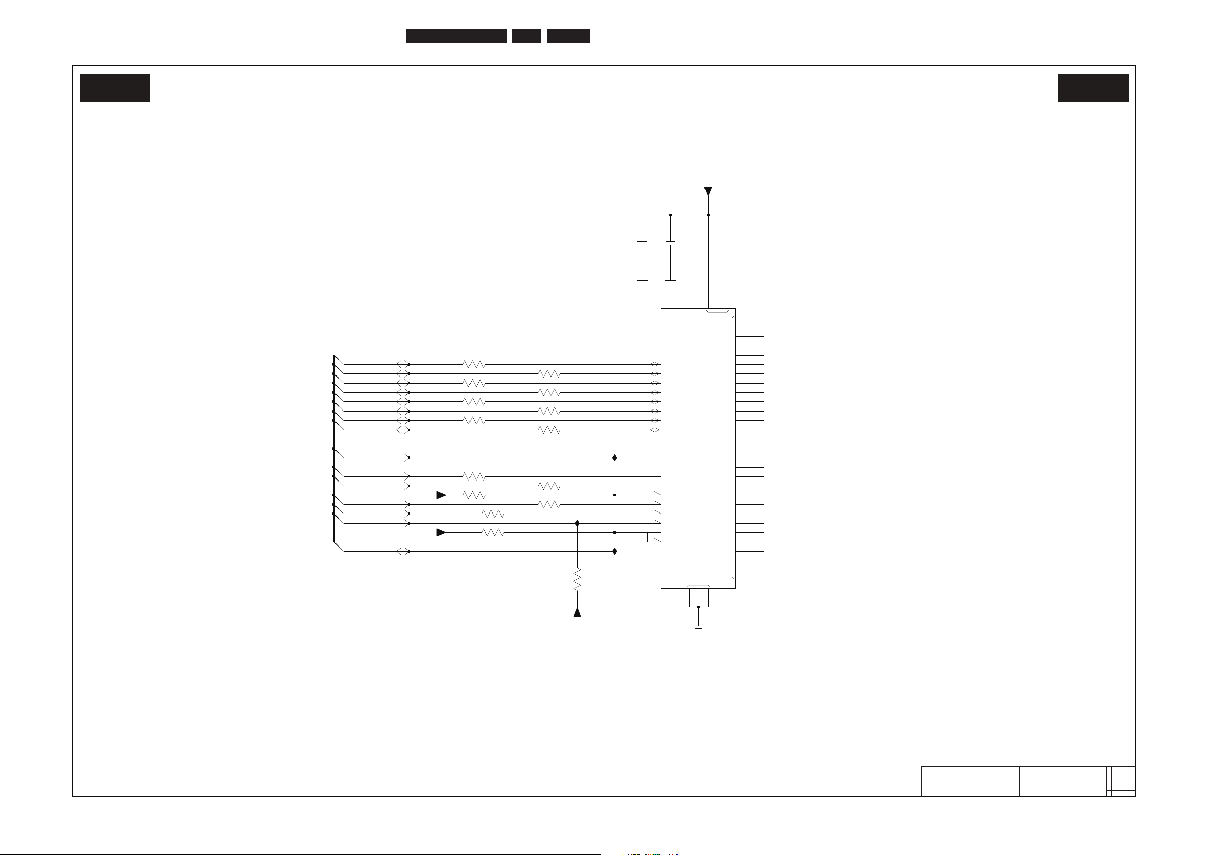
EN 74Q552.2L LA 10.
Circuit Diagrams and PWB Layouts
2011-Jul-15
back to
div. table
Flash
19110_011_110411.eps
110415
Flash
B01B B01B
2011-03-09
3
2010-12-23
2
3139 123 6521
SPB SSB TV550
2K11 4DDR BR SD
WE
B
R
WP
VCC
VSS
IO
NC
0
1
2
3
4
5
6
7
CLE
ALE
CE
RE
IF22
IF21
IF23
+3V3
100n
2F20
2F21
100n
18
19
3F23 10K
5
6
10
11
14
8
7
12
37
13
36
35
38
39
40
45
46
47
3
48
4
22
23
24
25
26
27
28
2
33
34
31
32
41
42
43
44
1
15
20
21
17
9
16
29
30
4G × 16
[FLASH]
Φ
NAND04GW3B2DN6F
7F20
2K2
+3V3
3F24
+3V3
+3V3
45
3F19
10K
100R3F22-4
3F22-1 100R18
100R3F22-3 3 6
27
45
3F22-2 100R
27
3F21-4 100R
5
100R3F21-2
3F20-4 100R4
100R3F21-3 3 6
100R18
3F20-3 3 6
3F21-1
27
100R
8
100R3F20-2
3F20-1 100R1
NAND-CE1n
NAND-RDY1n
NAND-WPn
XIO-D01
XIO-D00
XIO-D03
XIO-D02
XIO-D05
XIO-D04
XIO-D07
XIO-D06
NAND-ALE
NAND-CLE
XIO-OEn
XIO-WEn
Page 75
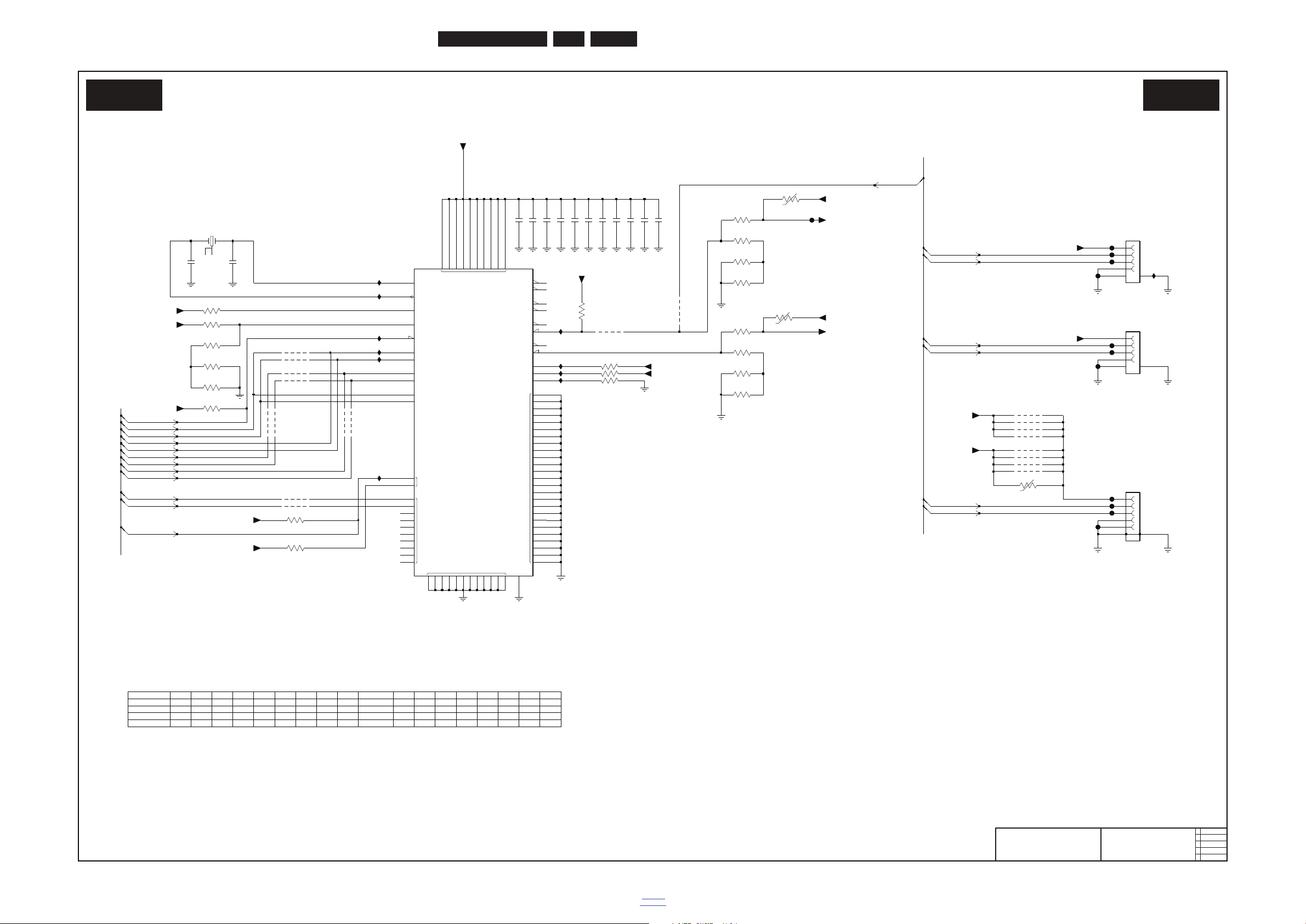
Circuit Diagrams and PWB Layouts
EN 75Q552.2L LA 10.
2011-Jul-15
back to
div. table
USB Hub
19110_012_110411.eps
110415
USB Hub
B01C B01C
2011-03-09
3
2010-12-23
2
3139 123 6521
SPB SSB TV550
2K11 4DDR BR SD
SPI_SCK
SPI_SD
VIA
VCC
GND
GND
HS
XIN
XOUT
SELFPWR
VBUSPOWER
RESET
DD+
DD1DD1+
DD2DD2+
RES
NC
GREEN1
AMBER1
GREEN2
AMBER2
PWR1
OVR1
PWR2
OVR2
SPI_CS
+T
+T
+T
Y
9FLF/G 9FLH/J 9FLK/L
YN
Y
3F32
Y
1P08
Y
1x USB
Y
Y
Y
3F34
CY7C65621
7FL5
N -
(WIFI)
Y
Y
NY
N
Y
N
N
N
Y
NNN
N
N
Y
Y
Y
Y
Y NN
N
Y
Y
9FL3
Y
N
YNNN
N
3FL7
Y
CY7C65621
CY7C65631
N
Y
N
NNN N N
1P07
Y
N
N
1F24
USB1
3FL2
2x USB + WIFI
USB2
9FLC/D
Y
Y
SCENARIO
NN
9F25/6
N
3FL4
Y
Y
N
Y
Y
3FLG
Y
9FLE
1x USB + WIFI
2x USB
N
9FL2
Y
N
18
100K
3FLE-1
10K
3FLD
9FL2-118
IFLE
FL41
IFLD
+5V
IFLC
2FLA
1n0
FL43
+3V3
2FLD
10n
10K
3FL7
15K
+5V
3FLB
3FLA 10K
10K3FLC
IFLG
3FLH
10K
9FLD
9FLC
9FLL
9FLJ
9FLK
3FLE-2
27
3FLE-4
100K
45
100K
36
IFL3
9FL2-3
9FL1-2RES 2 7
IFL1
9FL1-1RES 1 8
3FLG
10K
+3V3
10n
2FL5
+3V3
2FL2
100n
3FLE-3
100K
36
+5V
FL40
FL32
9FL2-445
IFL4
IFL2
9FL1-3RES 3 6
81
82
60
61
62
63
64
65
66
21
22
72
73
74
75
76
59
77
78
79
80
1923273339
58
67
68
69
70
71
45
25
48
49
26
3557
11
15
2
44
43
30
32
29
31
53
51
46
57
35
37
5
52
6
42
41
54
1
50
56
8
12162024283440
36
38
18
17
14
13
10
9
4
47
FL30
7FL5
CY7C65621-56LTXCT
FL38
FL39
3FL2
0R3
9FLH
+3V3
IFLB
9FLG
9FLF
36
FL31
100K
3FL4-3
FL36
2FL4
IFLF
100n
100n
2FL9
1u02FL8
18
+3V3
+5V
27
100K
3F34-1
100K
3F34-2
100n
2FL1
27
+5V-USB1
3FL4-1
18
100K
3FL4-2
+5V-USB2
100K
FL42
USB-16-PBT-B-30-CU1-BRF
1P07
1
2
3
4
5
6
9FL1-4RES 4 5
+3V3
9F25
+3V3
12p
2FL6
100K
3F34-4
4
10K
+3V3
4
13
3FLF
24M
1FL5
2
3FL4-4
45
+5V-USB1
67
+5V-USB2
100K
1F24
502386-0570
1
2
3
4
5
3F32
RES
0R3
9FL3
2FL7
12p
9FL2-227
0R3
3FLJ
FL33
RES
10n
2FL3
+3V3
9F26
IFLA
100K
36
1
2
3
4
5
6
3F34-3
USB-16-PBT-B-30-CU1-BRF
1P08
FL37
9FLE
2FLC
1n0
1n0
2FLB
USB2-DP
USB2-DM
USB-OVR1
USB2-DP
USB2-DM
USB-OVR1
USB-WIFI-DDn
USB-WIFI-DDp
USB-DP
RESET-USBn
USB1-DM
USB1-DP
USB-WIFI-DDn
USB-WIFI-DDp
USB-DM
USB1-DP
USB1-DM
USB2-DP
USB2-DM
Page 76
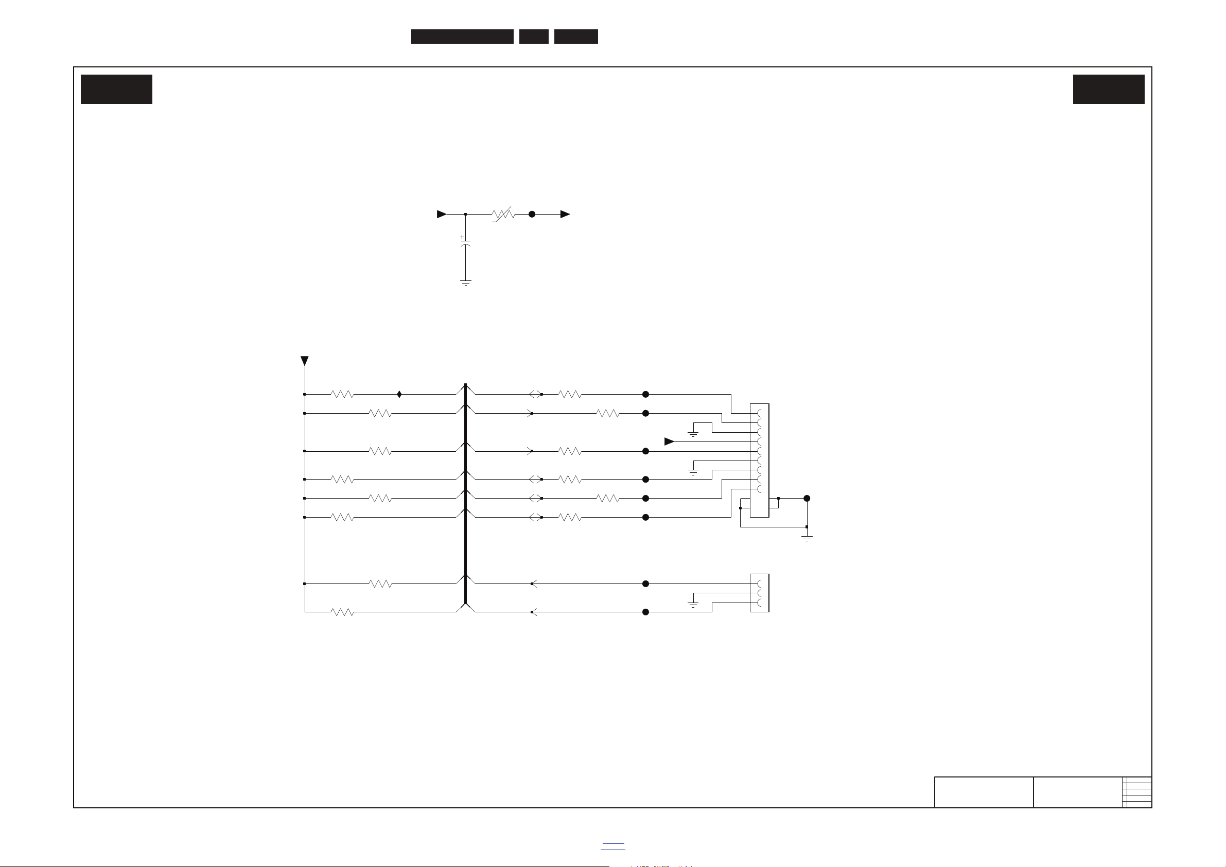
EN 76Q552.2L LA 10.
Circuit Diagrams and PWB Layouts
2011-Jul-15
back to
div. table
SD Card
19110_013_110411.eps
110415
SD-Card
B01D B01D
2011-03-09
3
2010-12-23
2
3139 123 6521
SPB SSB TV550
2K11 4DDR BR SD
+T
FF42
FF41
100R
3F44-2
27
FF48
3F43-2
100R
27
1P09-2
SCDA7A0200
10
11
12
FF45
27
+3V3
8
3F42-2
47K
3F41-1
47K
1
47K
3F41-3
36
+3V3-SD
3F44-3
36
100R
100R
3F43-3
36
IF47
+3V3-SD
16V
22u
2F40
FF49
FF50
FF47
18
0R3
3F40
3F44-1
100R
413181
15
16
100R
3F43-1
2
3
4
5
6
7
8
9
1P09-1
SCDA7A0200
1
6
FF46
47K
3F42-3
3
3F42-1
47K
18
47K
27
3F41-2
RES3F45
10K
3F41-4
45
47K
+3V3
FF43
FF44
SDIO-CMD
SDIO-DAT0
SDIO-DAT1
SDIO-DAT2
SDIO-CDn
SDIO-WP
SDIO-CLK
SDIO-DAT3
SDIO-CMD
SDIO-CLK
SDIO-DAT0
SDIO-DAT1
SDIO-DAT2
SDIO-CDn
SDIO-WP
SDIO-DAT3
Page 77
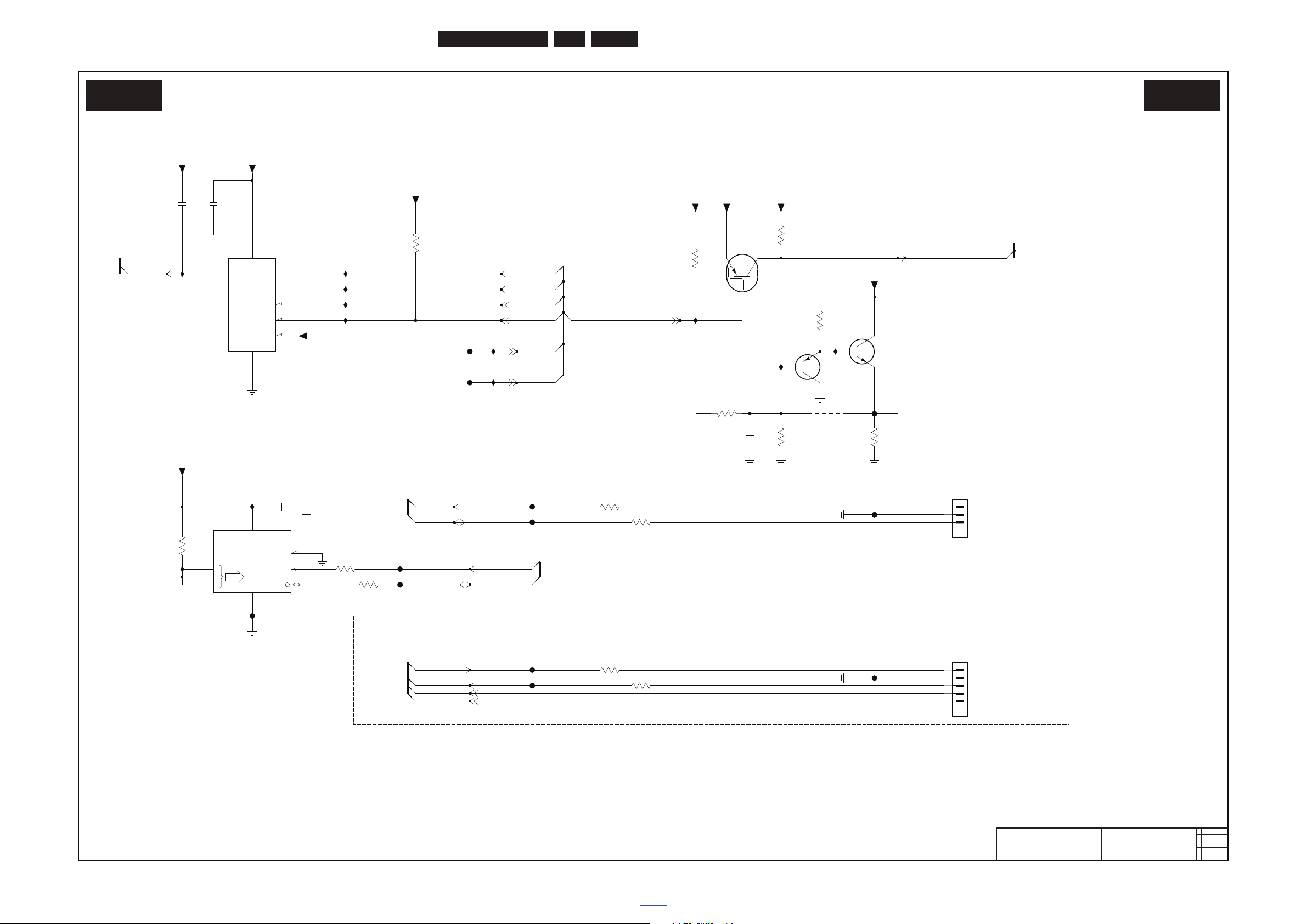
Circuit Diagrams and PWB Layouts
EN 77Q552.2L LA 10.
2011-Jul-15
back to
div. table
PNX85500 Control
19110_014_110411.eps
110415
PNX85500 Control
B01E B01E
2011-03-09
3
2010-12-23
2
3139 123 6521
SPB SSB TV550
2K11 4DDR BR SD
SCL
ADR
0
1
2SDA
WC
D
C
S
W
HOLD
VSS
Q
VCC
UP
DEBUG / RS232 INTERFACE
FOR
SCL
USE ONLY
LEVEL
DEBUG
MAIN NVM
SDA
SHIFTED
DEBUG ONLY
2F49
100p
100n
IF61
IF50
RES
2F58
IF57
100R
3F64
FF62
FF61
+3V3-STANDBY
+3V3-STANDBY
RES
100n
2F52
2
3
4
5
+3V3
1F52
RES
1
3F59
RES
PDTA114EU
7F53
3F60
100R
100R
3F67
FF57
10K
IF54
100R
3F65
10K
3F66
+5V
RES
47K
3F68
IF58
RES
7F52
M25P05-AVMN6
FLASH
512K
Φ
6
5
7
2
1
84
3
7F54-2
BC847BPN(COL)
5
3
4
+3V3
7
RES
(8K × 8)
1
2
3
6
5
84
Φ
EEPROM
7F58
3F63
+3V3
100R
10K
3F52
IF56
IF55
FF56
9CH0
10K
3F69
FF55
RES
IF52
FF66
FF29
FF04
IF51
3F54
1K0
IF53
RES
FF65
RES
1u0
2F53
FF64
3F53
5
67
10K
RES
1
2
3
4
3F58
10K
1F51
3F62
100R
FF63
IF59
+3V3-STANDBY
+3V3-STANDBY
2
6
1
RES7F54-1
BC847BPN(COL)
FF58
+3V3
IF62
PNX-SPI-SDO
PNX-SPI-CLK
RXD-UP
TXD-UP
SDA-SSB
SCL-SSB
SCL-UP-MIPS
SDA-UP-MIPS
PNX-SPI-WPn
PNX-SPI-CSBn
PNX-SPI-SDI
BOOST-PWM
SPI-PROG
RESET-STBYn
SDM
SPI-PROG
BACKLIGHT-BOOST
Page 78
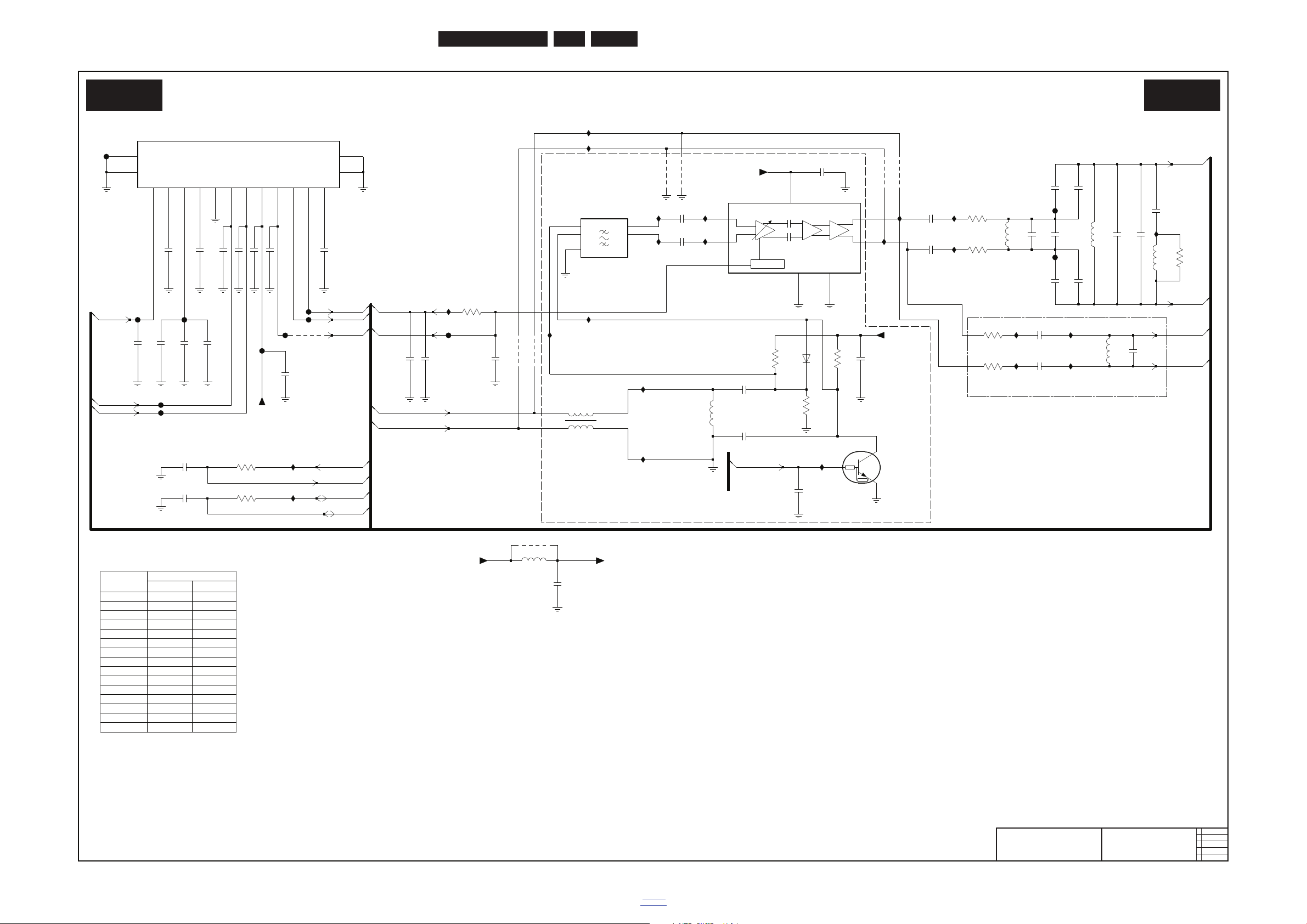
EN 78Q552.2L LA 10.
Circuit Diagrams and PWB Layouts
2011-Jul-15
back to
div. table
Tuner
19110_015_110415.eps
110415
Tuner
B01F B01F
2011-03-09
3
2010-12-23
2
3139 123 6521
SPB SSB TV550
2K11 4DDR BR SD
AGC CONTROL
I
O2ISWI
O1
GND
*
*
*
2F62
Used
1p0
*
FA23X7
560n
5F74
*
820n
680n
22p
RES
2F72
4u7
For BR NIM Tuner only
*
Remarks
1p0
2F82
Item No.
*
RES
*
9F04
1T01 TH26X3
15p
*
*
12p
2F80
*
RES9F03
15p
*
*
*
5p6
680n
Used
18p
5F71
9F02
2F61
*
RES
For EU Hybrid Tuner Only
Component
*
RES
2F73
RES9F05
9F06
RES
*
Used
*
10p
Brazil
Europe
RES
Used
Used
12p
2F77
3K3
PDTC114EU
7F70
3F78
1K0
3F72
4K7
10n
3F71
RES2F94
9F04
IF10
100n2F60
10n
2F71
AF73
+5V-TUN-PIN
2F75
10n
680n
5F66
IF72
FF00
IF14
2F72
3F82
820R
RES
+5V-TUN-PIN
IF86
2F64
10n
FF71
FF76
5F71
30R
5F72 RES
IF11
IF79
IF16
+5V-TUN-PIN
2F65
15p
1
FF01
RES
GND1
8
GND2
5
INPUT12
INPUT23
OUTPUT1 7
OUTPUT2 6
VAGC4
VCC
UPC3221GV-E1
7F75
15p
2F66
FF81
RES 2F9B
6p8
2F9D
6p8
RES
220R
3F80
FF74
6p8
2F97
2F77
RES
RES
2F76
2p2
RES
6p8
2F9C
2F93
100n
4K7
3F77
ATB2012
5F73
23
14
RES 5F76
330n
9F03
10n
2F79
9F71
RES 2F99
6p8
6p8
2F98
1415
16
12
NC
3
RF_AGC
1
RF_IO
4
TUN
RES
2
B+_LNA
B+_TUN
8
5
I2C_ADR
6
I2C_SCL
I2C_SDA
7
IF_OUT110IF_OUT2
11
13
1T01
TUNER
4MHZ_REF
9
+5V-TUN-PIN
3F79-1
220R
1
5F74
10n
2F90
AF72
9F05
36M17
1F75
X7251M
3
1
2
5
4
+5V-TUN
9F00
9F02
BA591
6F72
RES
6p8
2F9A
4
2F59 4n7
220R
3F79-4
2F63
10n
IF80
FF82
2F84
15p
220R
3F81
AF71
10n
2F74
RES
IF73
2F81
4n7
5F70
470n
3F75
47R
IF77
IF12
9F06
15p
2F86
FF75
IF15
IF81
AF70
RES
100p
2F96
IF89
IF90
9F01
2F80
47n
2F85
2F61
2F78
10n
2F88
22u
2F82
IF88
2F62
IF75
2F73
IF87
IF82
RES
1p0
2F70
RES
IF76
2F91
10n
IF78
IF13
IF74
RES 2F95
100p
10n
2F92
47R
3F76
SELECT-SAW
TUN-IF-N
TUN-IF-P
TUN-P6
TUN-P1
TUN-P7
PNX-IF-P
PNX-IF-N
IF-AGC
IF+
IF-
PNX-IF-AGC
TUN-IF-P
TUN-IF-N
IF-AGC
SCL-TUNER
TUN-P6
SDA-TUNER
TUN-P7
Page 79
Circuit Diagrams and PWB Layouts
EN 79Q552.2L LA 10.
2011-Jul-15
back to
div. table
Toshiba Supply
19110_016_110415.eps
110415
Toshiba supply
B01G B01G
2011-03-09
3
2010-12-23
2
3139 123 6521
SPB SSB TV550
2K11 4DDR BR SD
COM
OUTIN
+1V2-BRA-VDDC
+3V3
30R
30R
5FA3
5FA4
10u
2FA4
2FA3
100n
FFA2
FFAF
LD1117DT12
7FA3
1
32
100n
2FA2
+1V2-BRA-DR1
Page 80
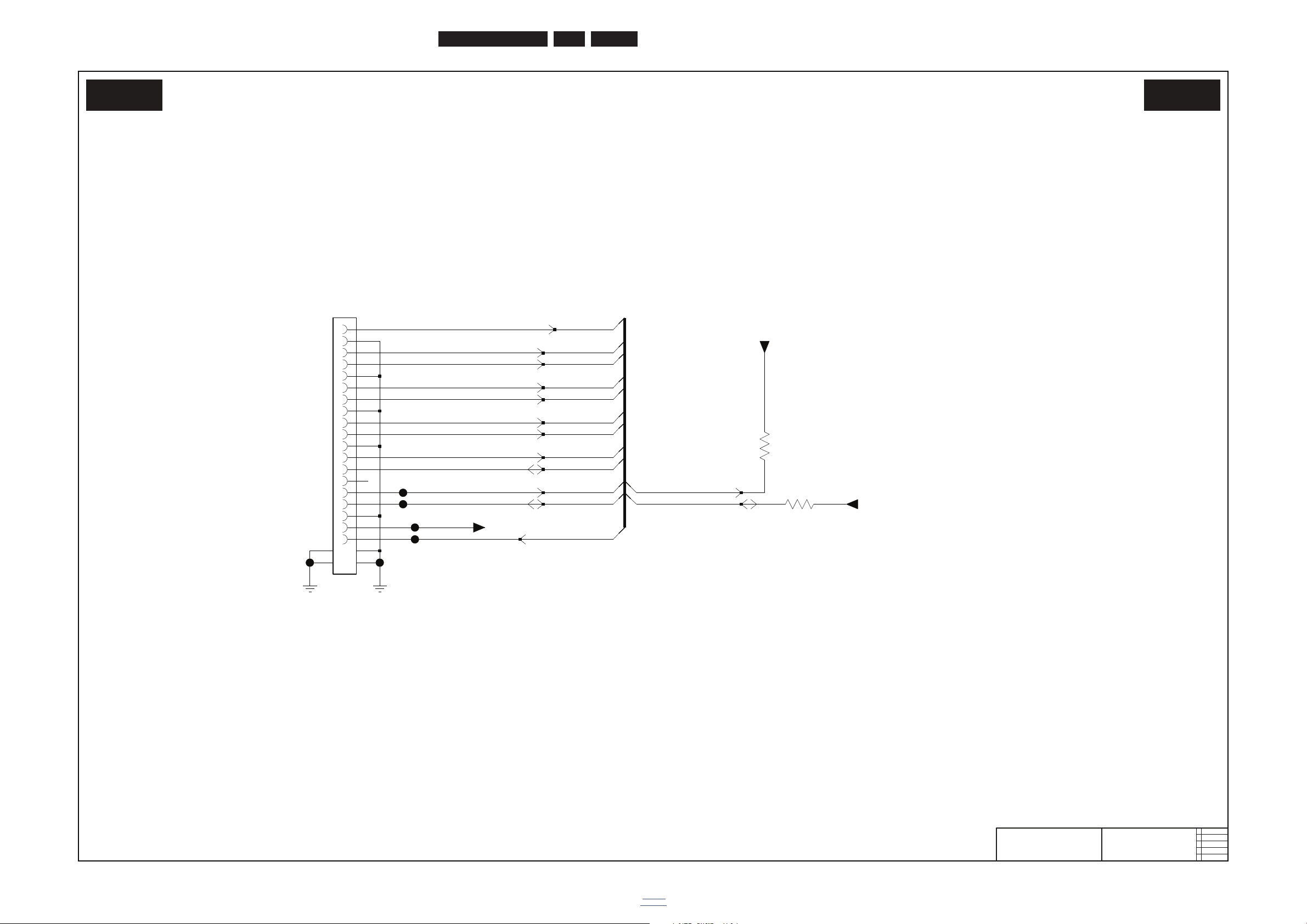
EN 80Q552.2L LA 10.
Circuit Diagrams and PWB Layouts
2011-Jul-15
back to
div. table
HDMI
19110_017_110415.eps
110415
HDMI
B01H B01H
2011-03-09
3
2010-12-23
2
3139 123 6521
SPB SSB TV550
2K11 4DDR BR SD
HDMI CONNECTOR SIDE
FFB3
47K
3FBF-2
27
18
DIN-5V
DIN-5V
3FBF-1
47K
FFB5
DIN-5V
FFB6
FFB4
FFB1
FFB2
2223
19
2
3
4
5
6
7
8
9
2021
1
10
11
12
13
14
15
16
17
18
1P05
DRX1-
DRX0+
DRX0-
DRX-DDC-SCL
DRX-DDC-SDA
DRX2+
DRXC+
DRXC-
PCEC-HDMI
DRX-DDC-SCL
DRX-DDC-SDA
DRX-HOTPLUG
DRX2-
DRX1+
Page 81
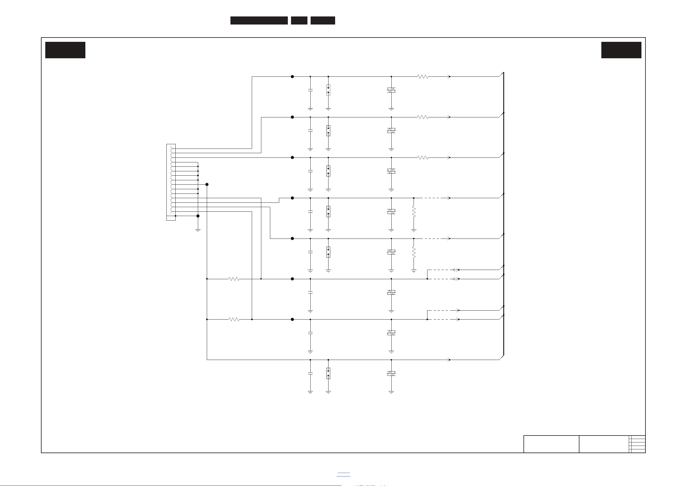
Circuit Diagrams and PWB Layouts
EN 81Q552.2L LA 10.
2011-Jul-15
back to
div. table
VGA
19110_018_110415.eps
110415
VGA
B01I B01I
2011-03-09
3
2010-12-23
2
3139 123 6521
SPB SSB TV550
2K11 4DDR BR SD
CONNECTOR
VGA
RES
12V
CDS4C12GTA
6FC4
9FC4
RES
2FC6
47p
FFC6
3FC1
RES
10K
RES 2FC2
100p
RES
12V
6FC5
CDS4C12GTA
RES
12V
CDS4C12GTA
6FC3
9FC1
RES
9FC2
FFC4
FFC8
FFC1
2FC1
100p
RES2FC8
47p
1FC1
4
5
6
7
8
9
1617
1216-02D-15L-2EC
1
10
11
12
13
14
15
2
3
1E05
9FC3
47p
2FC7
FFC9
6FC7
CDS4C12GTA
12V
RES RES
12V
CDS4C12GTA
6FC1
FFC5
9FC6
9FC5
1FC4
47p
2FC4
FFC7
3FC7
18R
18R
3FC6
CDS4C12GTA
6FC6
12V
RES
3FC5
18R
47p
1FC5
2FC5
10K
RES
3FC2
FFC3
RES
CDS4C12GTA
6FC2
12V
CDS4C12GTA
6FC8
4K7
RES
12V
3FC4
1FC3
4K7
3FC3
FFC2
1FC2
RES
1FC6
100p
2FC3
VGA-SCL-EDID
VGA-SDA-EDID
R-VGA
H-SYNC-VGA
V-SYNC-VGA
G-VGA
B-VGA
+5V-VGA
VGA-SDA-EDID-HDMI
VGA-SCL-EDID-HDMI
Page 82
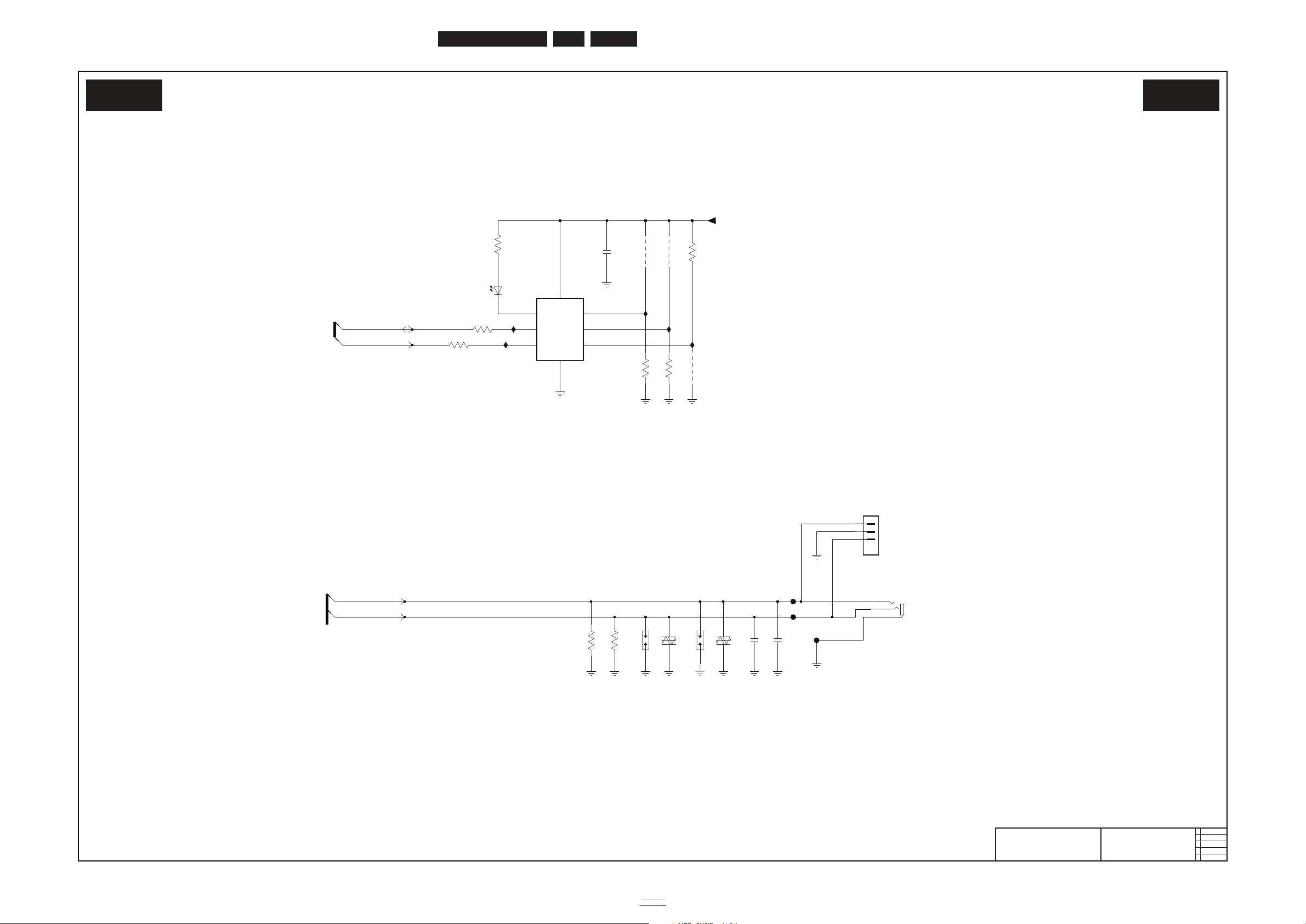
EN 82Q552.2L LA 10.
Circuit Diagrams and PWB Layouts
2011-Jul-15
back to
div. table
Temp sensor & headphone
19110_019_110415.eps
110415
Temp sensor & headphone
B01J B01J
2011-03-09
3
2010-12-23
2
3139 123 6521
SPB SSB TV550
2K11 4DDR BR SD
3FDG-2
27
FFDA
9FD2
1K0
RES
9FD1
RES
1K0
3FD7
1K0
3FD6
1329
1
2
3
45
502382-0370
RES
FFDC
6FD2
CDS4C12GTA
12V
RES
12V
1FD2
CDS4C12GTA
6FD3
RES
1FD3
22n
2FDC
2FDD
22n
3FD3
100R
3FD1
RES
IFD4
IFD2
1K0
6FD1
IFD5
LTST-C190KGKT
RES
IFD1
IFD3
3FD4
100R
2
1
3
MSJ-035-69A-B-RF-PBT-BRF
1328
100n
2FD1
RES
9FD5
3FD2
1K0
6
A1
A2
5
4
GND
OS
3
SCL
2
SDA
1
7FD1
LM75BDP
+VS
8
A0
7
+3V3
18
1K0
3FDG-1
AMP1
FFDB
SDA-SSB
SCL-SSB
AMP2
Page 83
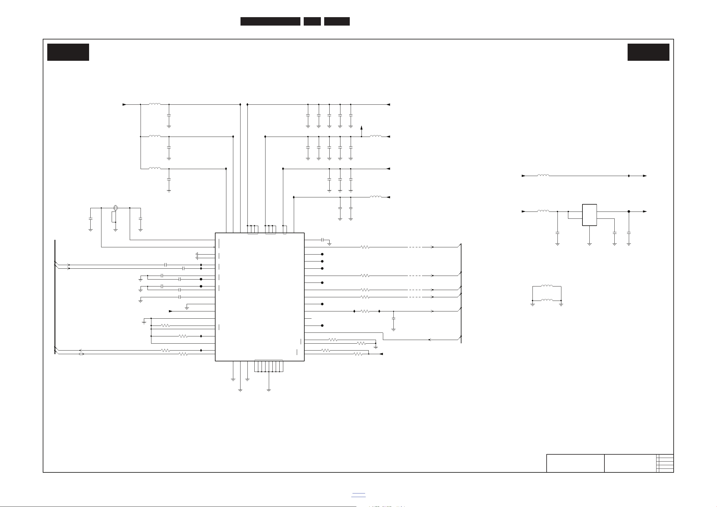
Circuit Diagrams and PWB Layouts
EN 83Q552.2L LA 10.
2011-Jul-15
back to
div. table
Tuner Brazil
19110_020_110415.eps
110415
Tuner Brazil
B01K B01K
2011-03-09
3
2010-12-23
2
3139 123 6521
SPB SSB TV550
2K11 4DDR BR SD
OUTIN
INH BP
COM
X
XSEL
ADI_AI
ADQ_AI
AD_VREF
TSMD
TN
SLADRS
VSS
DR2VDD
DR1VDD
VDDS
AD_DVDD
AD_AVDD
PLLVDD
VDDC
PBVAL
RERR
RLOCK
RSEORF
SBYTE
SLOCK
SRCK
SRDT
STSFLG1
AGCCNTI
AGCCNTR
STSFLG0
SYRSTN
0
1
SCL
SDA
FIL
AD_AVSS
AD_DVSS
PLLVSS
I
O
0
1
P
N
P
N
P
N
AD_VREF
DTCLK
DTMB
S_INFO
0
1
AGCI
CKI
SCL
SDA
*
*
* To be drawn near PNX85500
*
*
3
5
1u0
2FH2
4
2
1
33R3FG6-4 4 5
7FE3
LD3985M25
AGND
10n
2FH8
3FE5
18K
33R3FG6-2 2 7
2FH4
1u0
100n
2FE4
2FE3
100n
1u0
2FF1
2FE5
100n
100n
2FF0
1u0
2FE8
AGND
5FE5
30R
2FE0
1u0
18
3
2
5FE0
30R
4
15
333744
475057
62
19
1
41
16
365663
133549
64
5
52
61
60
51
38
42
8
12
14
58
20
17
53
54
55
59
45
46
6
24
9
10
7
11
34
48
43
39
40
21
29
30
27
28
2223
32
31
26
25
7FE0
TC90517FG
Φ
DFE8
DFE7
33R3FG6-3 3 6
DFE6
AGNDAGND
2FH5
1n5
18p
2FG3
AGND
4
13
2FG2
18p
25M4
1FE0
2
33R3FG7
DFE9
DFF2
DFF1
9F28
9F27-227
9F27-445
100n2FH6
2FG9 100n
2FG8 100n
2FG6 10n
10n2FG4
100n2FG7
AGND AGND
10K3FE7
3FE6 10K
AGND
AGND
AGND
2FH7 100n
IF49
BFE3
IF29
BFE2
IF18
1u0
2FF9
IF17
100n
2FF8
100n
2FF2
2FF3
100n
100n
2FF4
2FF6
1u0
2FF5
100n
5FE4
30R
IF68
IF69
AGND
IF66
1u0
2FE6
30R
5FE3
189F27-1
2FG1
1u0
100n
2FG0
5FE8
30R
2FF7
100n
AGND
5FG2
30R
100R3FE9
3FE8 100R
IF64
IF65
IF63
IF67
IF28
FF03
IF27
IF48
3FG2-2
10K
10K
3FG2-1
3FG4-1
4K7
4K7
3FG4-2
5FG0
30R
30R
5FE7
30R
10n
2FH3
5FE9
TS-FE-VALID
TS-BR-VALID
TS-FE-SOP
TS-BR-SOP
TS-FE-CLOCK
TS-BR-CLOCK
TS-FE-DATA
TS-BR-DATA
+3V3-BRA
+3V3-BRA-FLT
IF-
SCL-SSB
SDA-SSB
IF-AGC
+2V5-BRA
+5V
+3V3
+1V2-BRA-DR1
+3V3-BRA-FLT
RESET-SYSTEMn
+1V2-BRA-VDDC
+3V3-BRA-FLT
+3V3-BRA-FLT
+2V5-BRA
+3V3-BRA
+2V5-BRA
IF+
Page 84
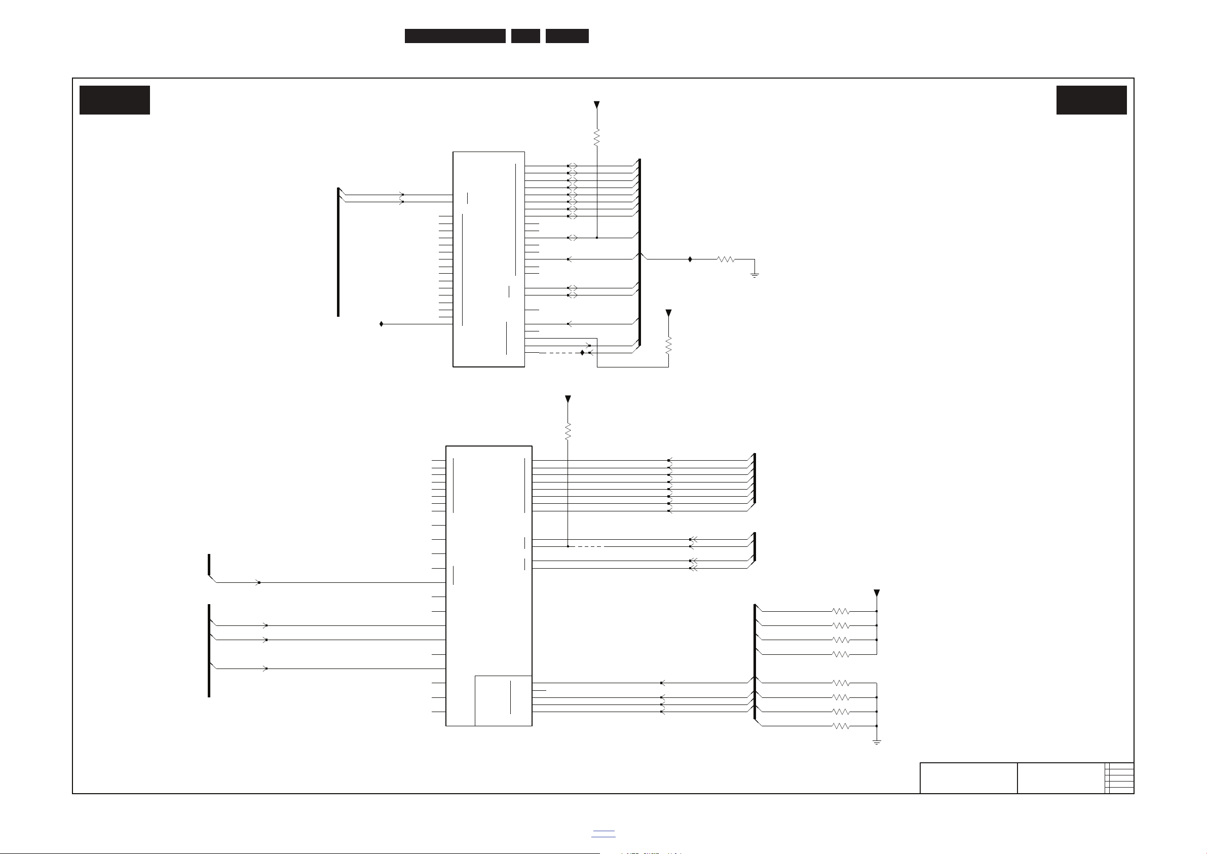
EN 84Q552.2L LA 10.
Circuit Diagrams and PWB Layouts
2011-Jul-15
back to
div. table
10-2 B02 313912365213
NANDflash - conditional access
19110_021_110415.eps
110415
PNX85500: NANDflash - conditional access
B02A B02A
2011-03-09
3
2010-12-23
2
3139 123 6521
SPB SSB TV550
2K11 4DDR BR SD
NAND
XIO_A
XIO_D
XIO
NAND
07
08
09
10
11
12
13
14
15
OE_
WE_
CLK_BURST
WP_
RDY1
RDY2
CE2_
CE1_
00
01
02
03
04
05
06
CLE
00
01
02
03
04
05
06
07
08
09
10
11
12
13
14
15
ALE
MDI
MCLK
MDO
TNR_SER1
VS
CD
CA
DATA
ERR
MICLK
MIVAL
SOP
0
1
2
3
4
5
6
7
1
2
1
2
VPPEN
0
1
2
3
4
5
6
7
ADD_EN
DATA_DIR
DATA_EN
I
O
MISTRT
MIVAL
MOSTRT
MOVAL
OOB_EN
RDY
RST
VCCEN
TS-FE-ERR
470R
3S23
3S1R
560R
560R
3S1S
IS26
560R
3S1U
RES
9S00
RES
10K
3S1V
RES
3S1T
560R
470R
3S28
IS25
RES
+3V3
IS00
+3V3
+3V3
3S1X
10K
3S1W
10K
3S24
470R
+3V3
9S08
L26
J23
J24
K23
K24
T21
T23
T22
R23
R22
M23
M24
M25
M26
L21
N24
N25
L22
L23
J21
L24
P22
P23
P24
P25
P26
N21
N22
N26
M21
M22
J22
K21
K22
K25
K26
N23
L25
P21
E26
D24
B22
C22
7S00-11
PNX85500
VIDEO_STREAM
D23
C23
B23
A22
E22
F24
F25
F26
E23
E24
E25
G22
G23
G24
G25
G26
F22
F23
D25
D26
C24
A20
A21
J25
J26
H21
H22
H23
H24
H25
H26
G21
FLASH
B21
D22
E21
D21
C21
F21
7S00-5
PNX85500
3S29
470R
RES
10K
3S15
TS-FE-CLOCK
TS-FE-VALID
TS-FE-SOP
INPACK INPACK
XIO-D10
CA-MOCLK
XIO-D00
XIO-D01
XIO-D02
XIO-D03
XIO-D04
XIO-D05
XIO-D06
XIO-D07
XIO-OEn
XIO-WEn
CA-RDY
NAND-ALE
NAND-CLE
NAND-CE1n
NAND-RDY1n
NAND-WPn
TS-FE-DATA
TS-FE-CLOCK
TS-FE-VALID
TS-FE-SOP
TS-FE-DATA
TS-FE-DATA
TS-FE-CLOCK
TS-FE-SOP
TS-FE-VALID
CA-MDO0
CA-MDO1
CA-MDO2
CA-MDO3
CA-MDO4
CA-MDO5
CA-MDO6
CA-MDO7
CA-MOVAL
CA-MOSTRT
CA-CD1n
CA-CD2n
CA-VS1n
CA-MOCLK
Page 85
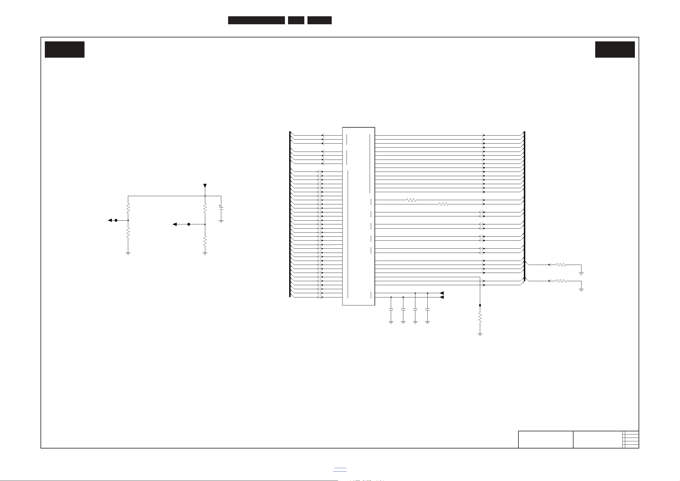
Circuit Diagrams and PWB Layouts
EN 85Q552.2L LA 10.
2011-Jul-15
back to
div. table
SDRAM
19110_022_110415.eps
110415
PNX85500: SDRAM
B02B B02B
2011-03-09
3
2010-12-23
2
3139 123 6521
SPB SSB TV550
2K11 4DDR BR SD
1
3
0
1
2
3
4
5
6
7
8
9
10
11
12
13
14
15
16
17
18
19
20
21
22
23
24
25
26
27
28
29
0
1
RASB
CASB
CKE
CSB
ODT
PCAL
0
1
2
3
4
5
6
7
8
9
10
11
12
13
14
N
P
N
P
30
31
0
1
2
2
DM
DQ
BA
A
CLK
DQS0
N
P
DQS1
N
P
DQS2
N
P
DQS3
VREF
M0
WEB
2
DDR2-VREF-CTRL2
+1V8
RES
3S6P
10K
FS02
DDR2-VREF-CTRL2
2S17
100n
IS42
10K
3S6Q
DDR2-VREF-CTRL3
DDR2-VREF-CTRL3
3S07
180R 1% 1%
180R
3S06
100p
2S24
100p
2S25
FS01
V1
H3
D3
D4
R1
R2
T3
T4
M4
M1
M5
A2
C3
R4
V5
B4
F1
C1
E1
F4
B2
E2
E3
N1
U1
P1
T1
V4
R5
U5
P5
N3
V3
E5
C5
A4
G5
B3
F5
U3
P2
U2
P3
F2
K3
K4
N5
N4
L5
D1
D5
R3
T5
F3
C2
G4
L3
G3
L2
H5
L1
J5
H1
H2
G1
MEMORY
PNX85500
7S00-8
J1
J3
J2
M3
J4
M2
K5
K1
1%
180R
3S22 3S20
180R 1%
100n
2S20
2.0V100u
2S12
10R
3S33
3S30
10R
1%
261R
3S0V
DDR2-ODTDDR2-RAS
DDR2-WE
DDR2-A13
DDR2-A14
DDR2-CKE
DDR2-DQS2_N
DDR2-DQS2_P
DDR2-DQS3_N
DDR2-DQS3_P
DDR2-BA2
DDR2-ODT
DDR2-DQM1
DDR2-DQM2
DDR2-DQM3
DDR2-DQS0_N
DDR2-DQS0_P
DDR2-DQS1_N
DDR2-DQS1_P
DDR2-D27
DDR2-D29
DDR2-D4
DDR2-D5
DDR2-D6
DDR2-D7
DDR2-D8
DDR2-D9
DDR2-DQM0
DDR2-D21
DDR2-D24
DDR2-D30
DDR2-D26
DDR2-D25
DDR2-D28
DDR2-D31
DDR2-D3
DDR2-D16
DDR2-D17
DDR2-D19
DDR2-D18
DDR2-D2
DDR2-D22
DDR2-D23
DDR2-D20
DDR2-D0
DDR2-D1
DDR2-D10
DDR2-D11
DDR2-D12
DDR2-D13
DDR2-D14
DDR2-D15
DDR2-A7
DDR2-A8
DDR2-A9
DDR2-BA0
DDR2-BA1
DDR2-CAS
DDR2-CKE
DDR2-CLK_N
DDR2-CLK_P
DDR2-CS
DDR2-A0
DDR2-A1
DDR2-A10
DDR2-A11
DDR2-A12
DDR2-A2
DDR2-A3
DDR2-A4
DDR2-A5
DDR2-A6
Page 86
EN 86Q552.2L LA 10.
Circuit Diagrams and PWB Layouts
2011-Jul-15
back to
div. table
Digital video in
19110_023_110415.eps
110415
PNX85500: Digital video in
B02C B02C
2011-03-09
3
2010-12-23
2
3139 123 6521
SPB SSB TV550
2K11 4DDR BR SD
RX0_A
RX1_A
P
N
RX2_A
RXC_A
P
N
DDC_A
P
N
P
N
HOT_PLUG_A
SDA
SCL
RREF
IS01
IS10
RES
2S2E
10u
+3V3
W26
W25
12K
3S0W
Y26
Y25
T24
W24
T26
T25
U26
U25
V26
V25
HDMI_DV
PNX85500
7S00-6
HDMIA-RX1-
HDMIA-RX2+
HDMIA-RX2-
HDMIA-RXC-
HDMIA-RXC+
DDCA-SCL
DDCA-SDA
HDMIA-RX0+
HDMIA-RX0-
HDMIA-RX1+
Page 87
Circuit Diagrams and PWB Layouts
EN 87Q552.2L LA 10.
2011-Jul-15
back to
div. table
Audio
19110_024_110415.eps
110415
PNX85500: Audio
B02D B02D
2011-03-09
3
2010-12-23
2
3139 123 6521
SPB SSB TV550
2K11 4DDR BR SD
&
&
&
&
OUT IN
INHBP
COM
AIN1
L
R
AIN2
L
R
AIN3
L
R
AIN4
L
R
AIN5
VR_AADC
ADAC
ADACL
P
N
ADACR
I2S_OUT
I2S_OUT_SD
SPDIF_OUT
POS
NEG
VREF_AADC
VCOM_AADC
SPDIF_IN1
4
3
2
1
2
N
P
1
3
4
5
6
WS
SCK
OSCLK
L
R
IS1S
1u0
2S30
22K
2
7
2
7
3S13-2
3S16-2
10K
2S3D
1n0
IS03
IS1N
IS0V
10K
3S34
3S37
10K
IS1Q
1R0
IS1P
+3V3
3S11
4V100u
2S41
3
2
1
4
11
+3V3
36
7S05-1
LM324
18
33R
3S3G-333R
3S3G-1
2S39
1n0
IS12
2S38
1n0
+24V-AUDIO-POWER
4
5
2S42
1u0
2S2V
3S16-4
10K
1u0
2S3Q
100n
2S3M
100n100n
2S3L
+24V-AUDIO-VDD
+3V3
10u
2S2S
4
2
1
3
5
RES
7S08
LD3985M25
FS08
10u
2S2R
56R
3S3F
7S09-4
74LVC00APW
12
13
714
11
9
10
714
8
14
6
74LVC00APW
7S09-3
7S09-2
74LVC00APW
4
5
7
1
2
714
3
74LVC00APW
7S09-1
220n
2S3J
IS1B
2S2H
47p
18
+24V-AUDIO-VDD
27
10K
3S36-1
3S36-2
10K
47p
2S2G
IS1K
2S3F
10u
2S3E
100n
100n
2S3G
22K
2
7
10K
3S16-3
3
6
3S12-2
1
8
2S2W
1u0
22K
3S12-1
2S3C
1n0
+24V-AUDIO-VDD
47R
3S6N
5
2S32
1u0
3S13-4
22K
4
3S17-227
2S31
10K
3
6
1u0
36
22K
3S13-3
10K
3S36-3
IS1H
1u0
2S34
4S14
RES
3S39
100R
100R
3S38
+3V3-ARC
IS1D
3S0Z
4R7
+2V5
DBS8
IS07
RES
27
+3V3
RES
36
220R
3S18-2
18
3S18-3
220R
220R
3S18-1
RES
+3V3
+3V3
100R
3S53-4
3S51
IS44
4R7
180R
3S6M
10K
68R
3S19
3S25
3S32
22K
3S6L
22K
11
IS1A
7S05-2
LM324
5
6
7
4
10
9
8
4
11
4
11
7S05-3
LM324
7S05-4
LM324
12
13
14
1
8
10K
3S16-1
2S2Y
1u0
2S36
+24V-AUDIO-VDD
1u0
10K
4
5
IS13
3S17-4
33R
3S3U
45
33R
3S3H
33R
3S3G-4
33R
3S3G-2
27
IS1J
18
AC8
AD8
AB8
AB9
3S17-1
10K
4DA8EA
AD1
AE1
AF2
AE3
AF3
AD2
AE5
AF5
AB6
AC6
AE10
AF10
AD10
AC10
AE9
AF9
AD9
AC9
AF8
AD7
AE7
AF7
AD6
AE6
AF6
AB7
AC7
AUDIO
7S00-2
PNX85500
IS1L
IS1G
+3V3-ARC
IS1E
+3V3-ARC
+3V3-ARC
18
IS0R
22K
3S13-1
1u0
2S2Z
1u0
2S33
2S2J
47p
45
47p
2S2K
3S36-4
10K
+2V5-AUDIO
IS1M
RES
9S06
3S10
100R
1u0
2S2L
10K
3
6
3S17-3
10u
2S3H
IS06
FS03
3S53-3
100R
IS02
100R
3S53-2
3S53-1
100R
1n0
2S3B
1n0
2S3A
2S2T
100n
IS19
100n
RES
eHDMI+
SPDIF-OPT
2S3K
ADAC(5)
ADAC(6)
SPDIF-OUT-PNX
SPDIF-OUT-PNX
SEL-HDMI-ARC
SPDIF-OUT
AUDIO-IN1-L
AUDIO-IN3-R
AUDIO-IN3-L
AUDIO-IN4-R
AUDIO-IN4-L
AUDIO-OUT-R
ADAC(6)
ADAC(4)
ADAC(3)
ADAC(2)
ADAC(1)
AUDIO-IN1-R
ADAC(1)
+AUDIO-L
-AUDIO-R
ADAC(2)
AUDIO-OUT-L
ADAC(5)
Page 88
EN 88Q552.2L LA 10.
Circuit Diagrams and PWB Layouts
2011-Jul-15
back to
div. table
MIPS
19110_025_110415.eps
110415
PNX85500: MIPS
B02E B02E
2011-03-09
3
2010-12-23
2
3139 123 6521
SPB SSB TV550
2K11 4DDR BR SD
USB
1
2
3
4
RREF
DP
DN
CLK_54_OUT
BL_PWM
RESET_SYS
TDI
TDO
TCK
TMS
TRSTN
SCL
SDA
SCL
SDA
SCL
SDA
SCL
SDA
ETHRXD
SDIO
DAT
ETH
TXD
TXCLK
0
1
2
3
TXEN
TXER
COL
CRS
MDC
MDIO
0
1
2
SDCD
SDWP
RXCLK
0
1
2
3
RXDV
RXER
CC_DAT3
CLK
CMD
-BUS
CTRL
FIL
I2C
INP
USE ONLY
FOR FACTORY
RES
61SI71SI
12
12
3S67
4K7
12
3S66
4K7
4K7
3S65
+3V3
100n
2S89
3S6G 2K2
+3V3
FS49
3S26
R24
10K
C25
B26
B25
B24
AA23
AB25
AB26
AA24
AA25
R26
R25
GPIO_4
W22
GPIO_5
GPIO_6
W23
V22
GPIO_7
AE4
C26
A25
A24
A23
AD5
AC5
GPIO_0
Y21
Y22
GPIO_1
V23
GPIO_10
GPIO_11
U23
Y23
GPIO_2
Y24
GPIO_3
W21
PNX85500
7S00-3
CONTROL
FS52
3S6E 2K2
IS08
+3V3-STANDBY
AB3W2
W1
W6
W5
W4
W3
U6
V6
AB4
AC1
AC2
Y4
AA2
AA1
AA4
AB1
AB2
AA5
ETHERNET
AC3
Y2
Y3
Y1
AA3
Y5
Y6
PNX85500
7S00-4
+3V3 +3V3
FS44
+3V3
10K
3S80
+3V3
FS11
IS09
DS52
3S40
10K
+3V3
3S64
10K
FS64
FS53
FS51
FS50
3S6C 4K7
IS4Z
RES
3S6J
10K
10K
3S6H-4
4
5
36
10K
3S6H-3
3S6K
10K
33R
3S00
2K23S6F2
2K23S6D
3S60
100R
1
3S5Z
100R
12
12
3S5W
100R
12
3S5Y
100R
12
3S571
2
3S58
100R
+3V3
100R
9S10
3S72
47R
3S55
5K6
9
10
1%
1
2
3
4
5
6
7
8
RES
BM08B-SRSS-TBT
1F10
10K
3S62
+3V3
VSS
IS04
SC0
SC1 8
4LCS1SD0
SD1 72SDA
3
VDD
6
7S01
PCA9540B
5
10K
3S21RES
FS10
3S27
10K
100R
12
+3V3
3S61
IS05
10K
3S45
9S09
+3V3
+3V3
3S83
10K
3S84
+3V3
10K
IS50
FS57
FS2Y
FS31
18
9S11
3S6H-1
10K
3S68
12
4K7
10K
3S82
FS2W
IS40
3S6B
+3V3
4K7
4K73S6A 4K7
3S69
9S13
2
9S12
100R
3S56
1
+3V3
+3V3
27
3S81
10K
3S6H-2
10K
BOOTMODE
SELECT-SAW
GPIO6
PNX-SPI-CS-BLn
BOOST-PWM
RXD1-MIPS
TXD1-MIPS
EJTAG-TDI-PNX85500
EJTAG-TRSTn-PNX85500
EJTAG-TMS-PNX85500
PXCLK54
TXD2-MIPS
RXD2-MIPS
3D-LR3D-LR
SCL-DISP
SDA-SET
SDA-DISP
SDA-BL
EJTAG-TMS-PNX85500
EJTAG-TRSTn-PNX85500
EJTAG-TCK-PNX85500
EJTAG-TDO-PNX85500
EJTAG-TDI-PNX85500
EJTAG-DETECTn
EJTAG-TDO-PNX85500
EJTAG-TCK-PNX85500
SCL-TUNER
RESET-SYSTEMn
SCL-DISP
SCL-BL
SCL-SET SDA-DISP
SDA-BLSDA-SET
SCL-DISP
SCL-BL
SDA-DISP
SDA-BL
SCL-SET
SCL-BL
SCL-UP-MIPS
SDA-SET
SCL-SET
SDA-SSB
SCL-SSB
SDA-TUNER
SCL-TUNER
SDA-UP-MIPS
SCL-UP-MIPS
SDA-SET
SCL-SET
SDA-SSB
SCL-SSB
SDA-TUNER
ETH-TXD(2)
ETH-TXD(3)
ETH-TXEN
ETH-TXER
ETH-COL
ETH-CRS
ETH-MDC
SDA-UP-MIPS
ETH-TXCLK
SDIO-DAT3
SDIO-CLK
SDIO-CMD
SDIO-DAT0
SDIO-DAT1
SDIO-DAT2
SDIO-CDn
SDIO-WP
ETH-TXD(0)
ETH-TXD(1)
ETH-RXCLK
ETH-RXD(0)
ETH-RXD(1)
ETH-RXD(2)
ETH-RXD(3)
ETH-RXDV
ETH-RXER
BACKLIGHT-PWM
BOOTMODE
BOOST-PWM
SELECT-SAW
RXD1-MIPS
TXD1-MIPS
RXD2-MIPS
TXD2-MIPS
GPIO6
PNX-SPI-CS-BLn
EJTAG-TCK-PNX85500
EJTAG-TDI-PNX85500
EJTAG-TDO-PNX85500
EJTAG-TMS-PNX85500
EJTAG-TRSTn-PNX85500
USB-DM
USB-DP
ETH-MDIO
Page 89
Circuit Diagrams and PWB Layouts
EN 89Q552.2L LA 10.
2011-Jul-15
back to
div. table
Video out - LVDS
19110_026_110415.eps
110415
PNX85500: Video out - LVDS
B02F B02F
2011-03-09
3
2010-12-23
2
3139 123 6521
SPB SSB TV550
2K11 4DDR BR SD
LOUT1
A
N
P
B
CLK
N
P
C
N
P
D
N
P
E
LOUT2
N
P
A
N
P
B
N
P
CLK
N
P
C
N
P
D
N
P
E
LOUT3
A
N
P
B
CLK
N
P
C
N
P
D
N
P
E
N
P
N
P
LOUT4
A
N
P
B
CLK
N
P
C
N
P
D
N
P
E
N
P
N
P
N
P
N
P
E18
E19
D19
D12
D14
E14
E15
D15
E17
D17
D16
E16
D18
D7
E7
E8
D8
E10
D10
D9
E9
D11
E11
E12
B14
C15
B15
C17
B17
A16
B16
A18
B18
C19
B19
B8
C10
B10
A9
B9
A11
B11
C12
B12
A14
LVDS
7S00-7
PNX85500
A7
B7
C8
9S90
9S91
9S92
9S93 9S97
9S95
9S96
9S94
PX3CLK+
PX3CLK-
PX4CLK+
PX4CLK-
PX1C+
PX1C-
PX1B+
PX1B-
PX1A+
PX1A-
PX2A+
PX2A-
PX1E+
PX1E-
PX1D+
PX1D-
PX1CLK+
PX1CLK-
PX2D+
PX2D-
PX2CLK+
PX2CLK-
PX2C+
PX2C-
PX2B+
PX2B-
PX3C+
PX3C-
PX3B+
PX3B-
PX3A+
PX3A-
PX2E+
PX2E-
PX4B-
PX4A+
PX4A-
PX3E+
PX3E-
PX3D+
PX3D-
PX4E+
PX4E-
PX4D+
PX4D-
PX4C+
PX4C-
PX4B+
Page 90
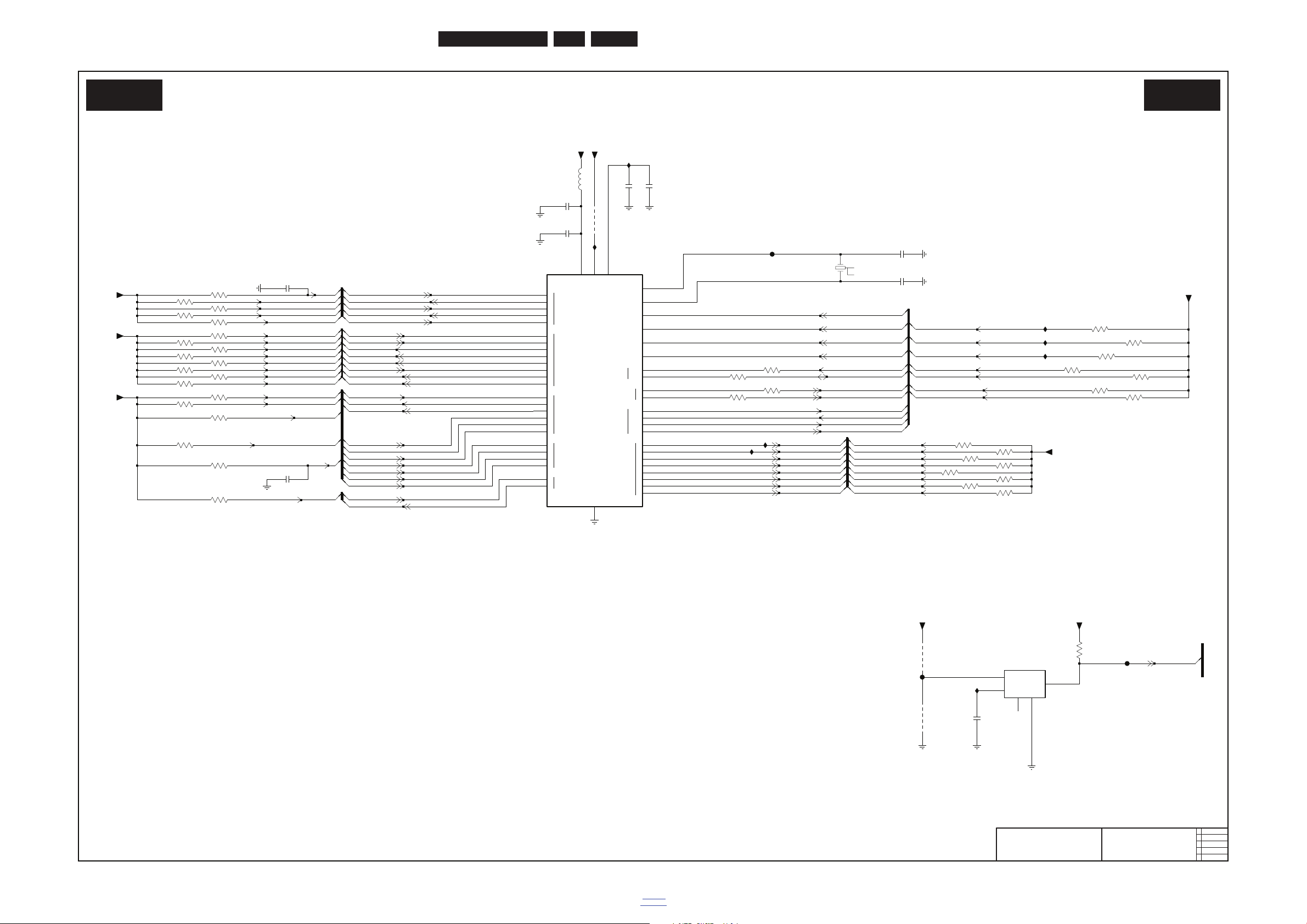
EN 90Q552.2L LA 10.
Circuit Diagrams and PWB Layouts
2011-Jul-15
back to
div. table
Standby controller
19110_027_110415.eps
110415
PNX85500: Standby controller
B02G B02G
2011-03-09
4
2010-12-23
2
3139 123 6521
SPB SSB TV550
2K11 4DDR BR SD
MC
PWM
SPI
P0
P1
P2
P3
P5
P6
3
4
5
0
1
2
3
4
5
VDD_XTAL
VDDA_ADC2V5
VDDA_1V1_DCS
0
1
2
3
7
0
1
2
3
4
5
6
7
0
1
2
7
VSS_XTAL
XTAL_IN
XTAL_OUT
RESET_IN
EA
ALE
PSEN
SDA
SCL
0
1
SDO
SDI
CLK
CSB
0
1
2
3
4
5
6
2S4D
1n0
100n
2S10
OUTP
1
2S4K
100n
5
CD
3
GND
INP
2
NC
4
NCP303LSN28
7S20
3S42
10K
1S02
2
4
1
3
54M
RES3S3Q
10K
RES 3S46
10K
10K
3S2M
RES
3S1K
10K
RES
10K
3S1G
3S1H
10K
10K
3S3P
RES
+3V3-STANDBY
3S3N
10K
RES
3S6W
4K7
DS50
1
+1V1
AF25
AE23
AA17
AF26
AC17
AD17
AE17
AF17
AE24
AF22
AE22
AC26
AD26
AC25
AA26
AC24
AC23
AF24
AF23
AD21
AE21
AF21
AA22
AB22
AC22
AD22
AD23
AE26
AE25
AE19
AF19
AA20
AB20
AC20
AD20
AE20
AF20
AA21
AB21
AC21
AB24
AB17
AA18
AD18
AE18
AF18
AA19
AB19
AC19
AD19
7S00-9
PNX85500
STANDBY
AB23
10K
3S44
10K
+3V3-STANDBY
3S43
12
9S0E
1K0
3S2V
FS0Z
10K
3S1L
+3V3-STANDBY
FS45
1
10K
RES
3S2A
IS3B
1u0
2S13
3S6VRES
4K7
IS20
9S24
RES
POL
IS3E
IS2Z
10K
RES
IS2V
3S2L
9S0D
RES
10K
3S3M
IS2U
100R3S2K
+3V3-STANDBY
100R3S2G
3S2F 100R
10K
RES
+3V3-STANDBY
3S1P
10p
2S4G
3S1B
10K
3S1D
27K
10K
3S1C
RES
10K
RES
3S3L
4K7
3S49
10K
3S3R
RES
+3V3-STANDBY
1u0
2S37
100n
2S11
3S3S
10K
RES
+3V3-STANDBY
3S3W
4K7
RES
2S4E
100n
3S1J
100K
IS3D
RES
3S2S
10K
10K
3S3T
RES
3S47
10K
10K
3S3YRES
3S2H 100R
10K
3S41
2S4F
10p
3S1F
10K
RES
10K
3S1E
5S04
RES
30R
IS3F
SDA-UP-MIPS
SCL-UP-MIPS
SPI-PROG
RESET-AVPIP
RESET-STBYn
PNX-SPI-WPn
SPI-PROG
DETECT2
RESET-STBYn
CTRL-DISP
SEL-HDMI-ARC
LCD-PWR-ONn
EJTAG-DETECTn
LAMP-ON
STANDBY
FAN-CTRL1
FAN-CTRL2
POWER-OK
ENABLE-3V3n
AV1-STATUS
AV2-STATUS
LED2
PSEN
ALE
EA
RESET-DVBS
RESET-USBn
RESET-ETHERNETn
RESET-AUDIO
AUDIO-MUTE-UP
BACKLIGHT-PWM-ANA-DISP
SDM
RXD-UP
TXD-UP
RESET-SYSTEMn
KEYBOARD
SDA-UP-MIPS
SCL-UP-MIPS
LED1
LED2
LED1
PSEN
PNX-SPI-CLK
PNX-SPI-CSBn
PNX-SPI-SDI
PNX-SPI-SDO
KEYBOARD
LIGHT-SENSOR
RC
TACHO
CEC-HDMI
ALE
EA
CTRL-DISP
RESET-DVBS
RESET-USBn
RESET-ETHERNETn
SEL-HDMI-ARC
RESET-AVPIP
RESET-AUDIO
AUDIO-MUTE-UP
RC
TACHO
CEC-HDMI
BACKLIGHT-PWM-ANA-DISP
SDM
LCD-PWR-ONn
EJTAG-DETECTn
LAMP-ON
STANDBY
FAN-CTRL1
FAN-CTRL2
POWER-OK
ENABLE-3V3n
RXD-UP
TXD-UP
DETECT2
RESET-SYSTEMn
AV2-BLK
AV1-BLK
Page 91
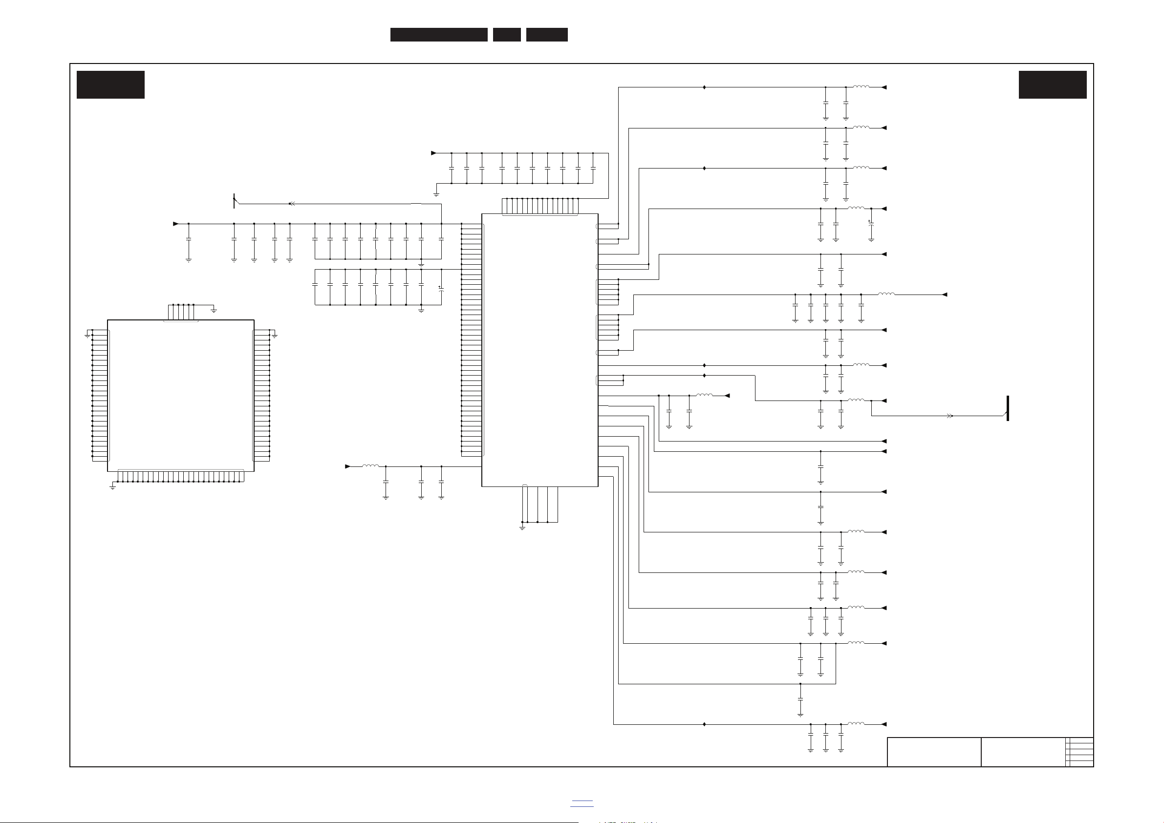
Circuit Diagrams and PWB Layouts
EN 91Q552.2L LA 10.
2011-Jul-15
back to
div. table
Power
19110_028_110415.eps
110415
PNX85500: Power
B02H B02H
2011-03-09
3
2010-12-23
2
3139 123 6521
SPB SSB TV550
2K11 4DDR BR SD
VDDA_2V5
HDMI_VDDA_3V3_TERM
VDDA_2V5_LVDS_BG
VDDA_2V5_USB
VDDA_2V5_VADC
VDDA_2V5_VDAC
VDDA_3V3_USB
VDD_1V1
VDD_1V8
HDMI_VDDA_1V1
HDMI_VDDA_2V5
VDD_2V5
VDD_2V5_LVDS
VDD_3V3
VDD_3V3_SBY
VDDA_1V2
VSSA_USB
VSSA_2V5_LVDS_BG
VSSA_1V1_LVDS_PLL
HDMI_AGND
VDD_1V1_DDR
VDDA_2V5_DCS
VDDA_2V5_ADAC
VDDA_2V5_AADC
VDDA_1V1_LVDS_PLL
VSSA
VSS
VSS
VSS
+2V5
100n
2S43
2S56
1u0
10u
2S5D
RES
2S58
10u
10u
RES
30R
5S82
2S4S
22u
2S4R
2S4M
220u 6.3V
100n
2S67
2S66
100n
100n
2S64
2S65
100n
100n
2S63
30R
5S85
2S61
100n
100n
2S6F
12
Y8
Y19
Y18
A13
C13
R20
C7
C9
C11
C14
C16
C18
W20
P20
M20
K20
V7
G7
L7
R6
R7U7A5
A6B5B6
N6
N7
G11
F13
J7
L6
C6D6E6F6G6
F7
U15
U17
J6
AA6
Y7
W7
F9
G9
AB5
H20
F11
N15
N17
R9
R11
R13
R15
R17
U9
U11
U13
AC4
J17
L9
L11
L13
L15
L17
N9
N11
N13
AD3
F15
G15
F17
G17
F19
G19
J9
J11
J13
AE2
J15
AA9
AA7
Y17
D13
T20
Y13
Y10
R21
AF1
G13
V24
V20
V21
U20
U21
U22
B13
AA15
Y15
AA13
Y12
VDD
PNX85500
7S00-10
U24
100n
2S4Z
IS3K
30R
5S84
5S94
30R
45
2S62
100n
2S5J-4
100n
100n
2S28
12
2S6H
100n
2S27
100n
100u
2S26
2S21
1u0
1u0
2S4Y
RES
5
30R
5S92
2S5K-4
100n
4
5S89
30R
+2V5
+2V5-LVDS
30R
5S88
2S57
10u
+1V1
100n
2S60
IS58
30R
5S80
c001
2S53
10u
+3V3
+2V5
100n
2S5C
2
+2V5
2S5B
10u
RES
2S4Q
22u
+1V1
2S4T
100n
100n
100n
3
6
2S68
2S29
220u 2.5V
2S5J-3
45
100n
2S5H-4
100n
2S5H-3
36
18
100n
2S5H-1
6
5S90
30R
2S5G-3
100n
3
2S46
100n
100n
2S45
5S93
30R
+1V1
+1V2
+2V5-LVDS
2S4N
100n
100u
2S23
V2
A3
Y20
A8
AA16
AA8
Y11
Y14
Y16
Y9
T18
A26
T2
T6
T7
U4
V10
V12
V14
V16
V18
A19
P16
P18
P4
P6
P7
T10
T12
T14
T16
A17
M14
M16
M18
M6
M7
N2
N20
P10
P12
P14
A15
K14
K16
K18
K2K6K7
L20
L4
M10
M12
G18G2G20
G8
H4H6H7
J20
K10
K12
F12
F14
F16
F18
F20
F8
G10
G12
G14
G16
A12
B1
B20
C20
C4
D2
D20
E13
E20
E4
F10
A10
7S00-12
PNX85500
VSS
A1
2S6P
2SHW
10u
+2V5-AUDIO
100n
c000
100n
2S6N
12
POL
12
2S4W
100n
2S6K
100n
100n
2S5M
100n
2S6E
1
2
12
12
2S6D
100n
18
100n
2S5P
100n
2S5G-1
27
+1V1
2S5J-2
100n
10u
2S55
100n
+2V5
+2V5-AUDIO
2S4P
10u 6.3V
2S52
2S51
100n
5S81
30R
IS3Q
10u
2S5A
RES
+3V3
100n
2S5J-1
1
8
100n
2S5K-3
36
100n
2S5K-2
27
2S5K-1
18
5S95
30R
100n
IS3L
+2V5
10u
2S50
2S4V
10u
2S4U
+3V3-STANDBY
+3V3
100n 100n
2S6C
12
IS3S
12
2S6G
100n
12
5S83
30R
12
100n
2S6L
2
100n
2S6M
100n
1
100n
2S6A
12
2S6B
27
1u0
2S59
2S5H-2
100n
45
5S87
30R
2S5G-4
100n
27
2S5G-2
100n
+1V8
SENSE+1V1
SENSE+1V2
Page 92
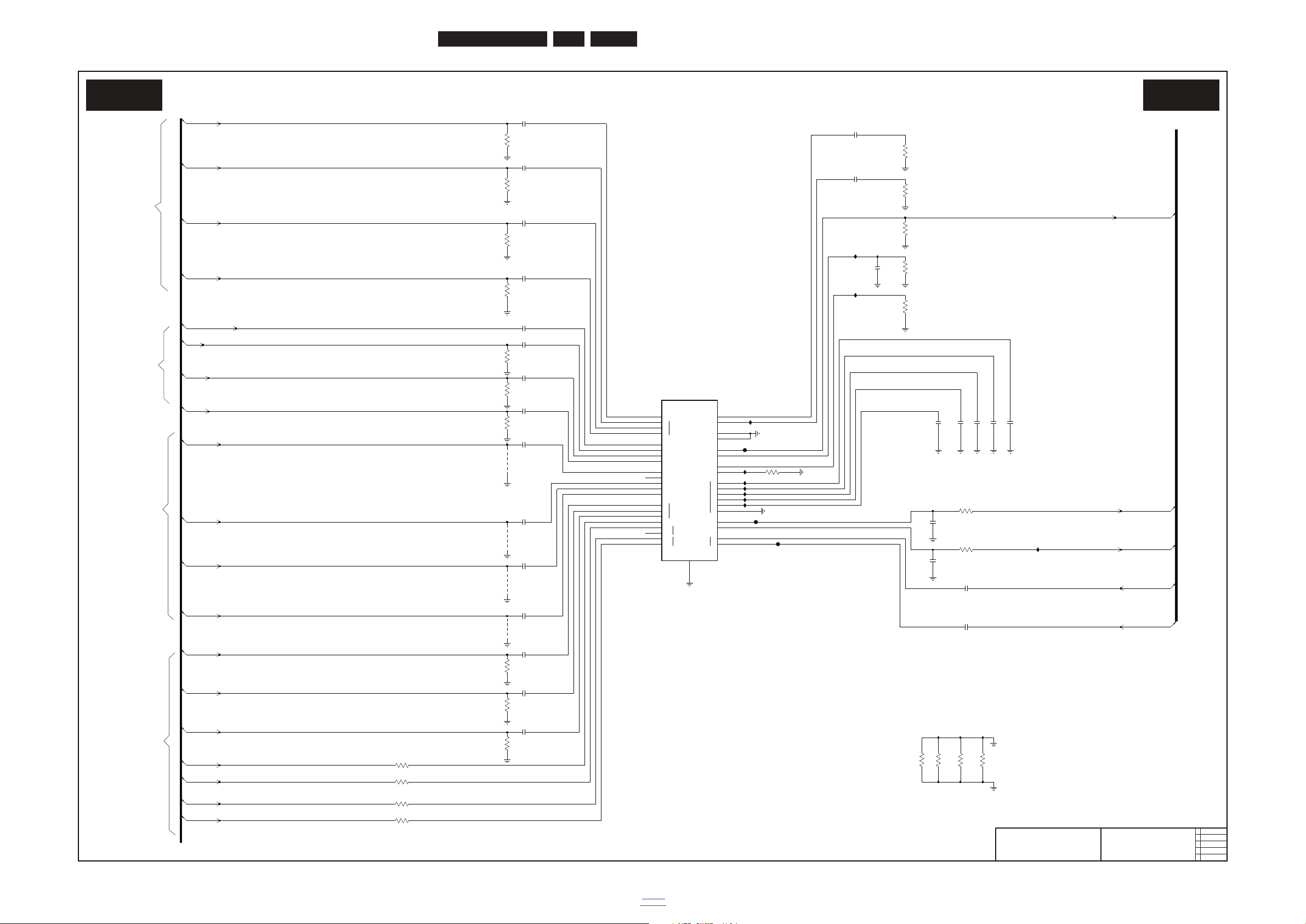
EN 92Q552.2L LA 10.
Circuit Diagrams and PWB Layouts
2011-Jul-15
back to
div. table
Analog video
19110_029_110415.eps
110415
PNX85500: Analog video
B02I B02I
2011-03-09
3
2010-12-23
2
3139 123 6521
SPB SSB TV550
2K11 4DDR BR SD
CVBS_Y7
C7
6
IN
OUT
SCL
SDA
ANALOG_VIDEO
AV1
VGA
ATV_CVBS_Y3
C3
CVBS1_OUT
CVBS2_OUT
RESREF
REF
TUNER
VGA_EDID
VSYNC
CURREF
1
2
3
4
5
IF_AGC
RF_AGC
P
N
AGND
CVBS_Y1
R
B
G
SYNCIN1
Y_G1
PR_R_C1
PB_B1
CVBS_Y2
SYNCIN2
Y_G2
PR_R_C2
PB_B2
R
G
B
HSYNC_IN
EU:
AP:
+CVBS
AP:
YPBPR1
YPBPR2
VGA
-
YPBPR1
AP:
SCART2
AP:
EU:
VGA
* 319803104790 - RST SM0402 47R PMS Col R at 9S18 for BRZ
EU:
Connectivity
EU:
SCART1
*
2S7L
22n
2S15
22n
2S14
22n
10n
2S76
56R
3S50
56R
3S4R
56R
3S4L
56R
3S4K
3S75
10K
9S19
3S5T-4
100R
45
3S4P
56R
2S7H
22n
3S5E
560R
IS5H
3S5B
47R
22n
2S87
IS4W
3S4J
56R
22n
2S86
22n
2S7K
9S21
2S8G
22n
3S59
22n
2S7R
47R
2S85
22n
2S7P
22n
BS10
22n
2S7N
36
10n
2S7M
8
3S5T-3
100R
3S5T-1
100R
1
2S18
22n
2S8A
22n
56R
3S54
10K
3S5S
IS5C
2S7J
22n
3S52
56R
2S84
AD25
AF15
AF14
AF12
AE12
AC18
AF4
AE15
AE14
22n
AC14
AC16
AB16
AB13
AB12
AA12
AA10
AB10
AB11
AF16
AD24
AF11
AE11
AB15
AB14
AD11
AD16
AB18
AD12
AD15
AD14
AC15
AA14
AC12
AD13
AE13
AC13
AE16
AF13
AC11
AA11
PNX85500
7S00-1
2S7U
22n
IS11
9S18
27
47p
2S40
3S5T-2
100R
8K2
3S09
3S4T
56R
2S19
22n
IS5G
IS5F
560R
3S08
BS13
9S20
2S77
10n
47K
3S76
IS4V
3S5V-3
RES
36
8
100R
3S5V-1
100R
RES
1
IS5J
2S16
22n
IS5D
IS5E
22n
2S7E
2S22
3S05
56R
22n
BS15
2S75
10n
10n
2S78
3S5V-2
100R
27
45
C-SVHS
3S5V-4
100R
PNX-RF-AGC
PNX-IF-AGC
H-SYNC-VGA
V-SYNC-VGA
VGA-SCL-EDID
VGA-SDA-EDID
AV3-PB
AV2-CVBS
AV4-Y
AV4-PR
R-VGA
G-VGA
B-VGA
Y-SVHS
AV1-G
AV1-CVBS
AV1-B
AV1-R
AV3-Y
YPBPR1-SYNCIN1
AV3-PR
CVBS-MON-OUT1
PNX-IF-P
PNX-IF-N
AV4-PB
Page 93
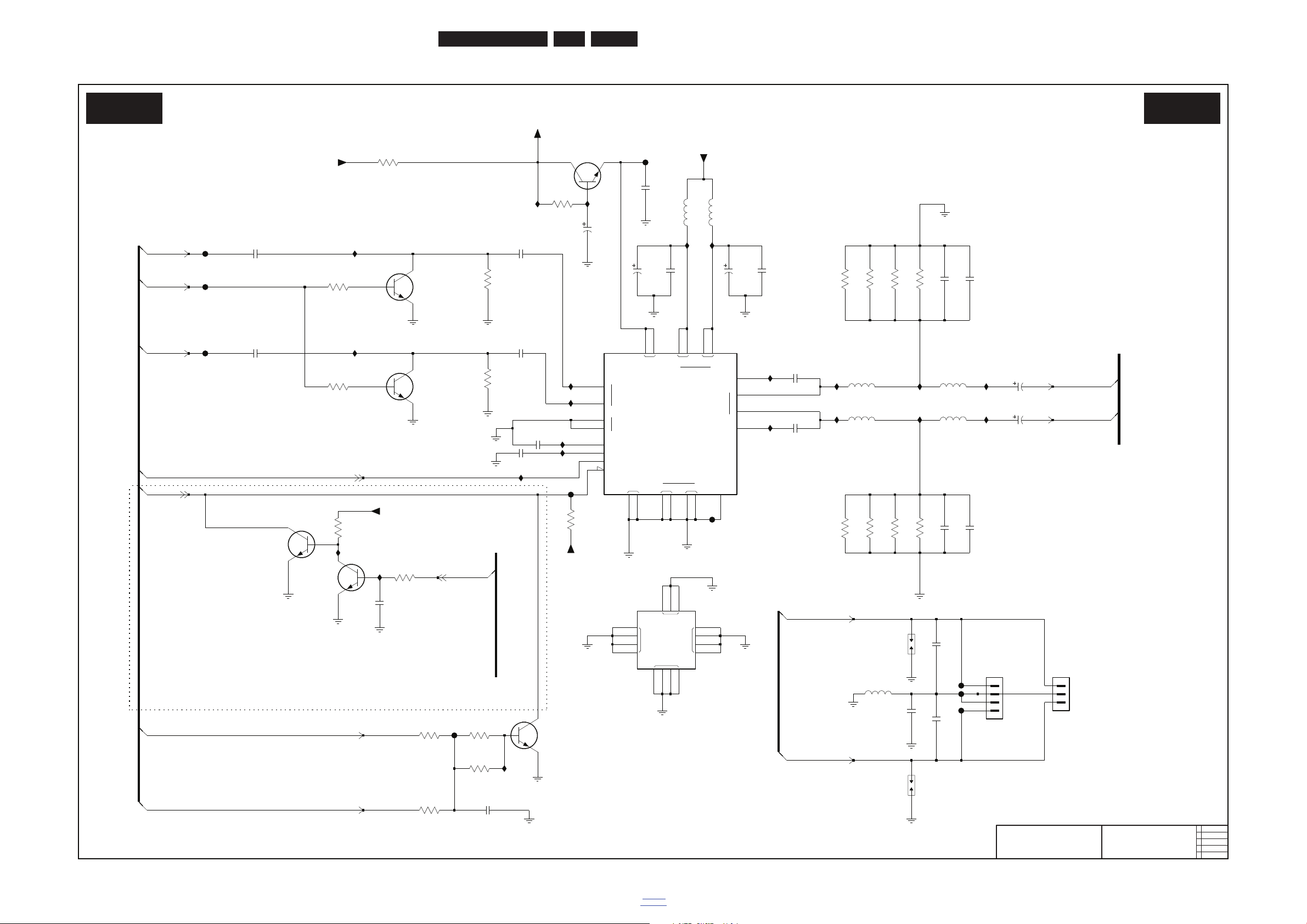
Circuit Diagrams and PWB Layouts
EN 93Q552.2L LA 10.
2011-Jul-15
back to
div. table
10-3 B03 313912365213
Audio
19110_030_110415.eps
110415
Audio
B03A B03A
2011-03-09
3
2010-12-23
2
3139 123 6521
SPB SSB TV550
2K11 4DDR BR SD
VIA VIA
VIA
VIA
VCLAMP
MUTE
IN
BSL
SD
R
AVCC
L
BSR
GND_HS
L
PGND
AGND L R
L
OUT
R
BYPASS
1
R
0
PVCC
GAIN
MAINS SWITCH DETECT
7
2
81
22K
3D10-2
3D10-1
22K
3D06-2
7
2
ID19
100K
ID32
220R
5D05
BC847BS(COL)
7D03-2
5
3
4
GND-AUDIO
2D28
1u0
CD10
ID29
ID31
22K
54
3D14-4
2D12
220u35V
5D04
220R
ID18
5D08
220R
220R
5D07
ID28
GND-AUDIO
35V 220u
2D11
47n
2D23
ID05
3D16
22K
ID15
FD02
2D13
10n
63
ID14
22K
3D10-3
35V
220u
2D20
220u
2D19
1
ID11
35V
7D03-1
BC847BS(COL)
2
6
ID37
FD09
63
FD08
36
4K7
3D02-3
4
3D01-3
47K
5
ID06
3D10-4
22K
GND-AUDIO
V_NOM
1D50
V_NOM
1D52
ID07
ID08
6
3
FD05
+3V3-STANDBY
3D14-3
22K
81
GND-AUDIO
22K
3D14-1
35V
10u
2D29
1u0
2D05
220R
5D03
2D24
47n
220n
2D22
+AVCC
GND-AUDIO
GND-AUDIO
5D01
22u
2D10
220n
220n
2D09
220n
2D06
2D17
1u0
ID27
ID35
FD14
72
GND-AUDIO
FD07
3D02-2
4K7
4K7
3D02-4
54
+3V3-STANDBY
1
4K7
3D02-1
8
FD01
5
2D02
10u
3D06-4
4
100K
36
100K
4K7
3D15
3D06-3
RES
ID33
GND-AUDIO
GND-AUDIO
220n
2D27
2D01
10n
ID09
RES
FD06
220n
2D26
2D03
100p
1u0
2D16
3D14-2
22K
7
2
2
6
1
GND-AUDIO
BC847BS(COL)
7D11-1
2D07
220n
220n
2D08
+24V-AUDIO-POWER
+24V-AUDIO-POWER
ID10
ID34
54
GND-AUDIO
47K
3D01-4
2D21
220n
81
100K
3D06-1
1
2
3
ID30
GND-AUDIO
2041145-3
1D38
GND-AUDIO
GND-AUDIO
GND-AUDIO
10n
2D14
4R7
3D09
GND-AUDIO
5
3
4
2
6
1
7D15-2
BC847BS(COL)
7D15-1
BC847BS(COL)
FD10
1
31012
6
15
2
11
17
25
5
22
4
23
24
13
14
8
9
19
20
21
16
7
18
AUDIO AMP
Φ
CLASS-D
TPA3123D2PWP
7D10-1
22u
5D02
ID12
FD03
28
29
30
31
32
33
34
26
35
36
37
38
39
40
27
VIA
7D10-2
TPA3123D2PWP
1
2
3
4
3
4
2041145-4
1735
BC847BS(COL)
7D11-2
5
DETECT2
AUDIO-MUTE-UP
-AUDIO-R
+AUDIO-L
A-STBY
RIGHT-SPEAKER
LEFT-SPEAKER
LEFT-SPEAKER
RIGHT-SPEAKER
LEFT-SPEAKER
RIGHT-SPEAKER
A-PLOP
Page 94
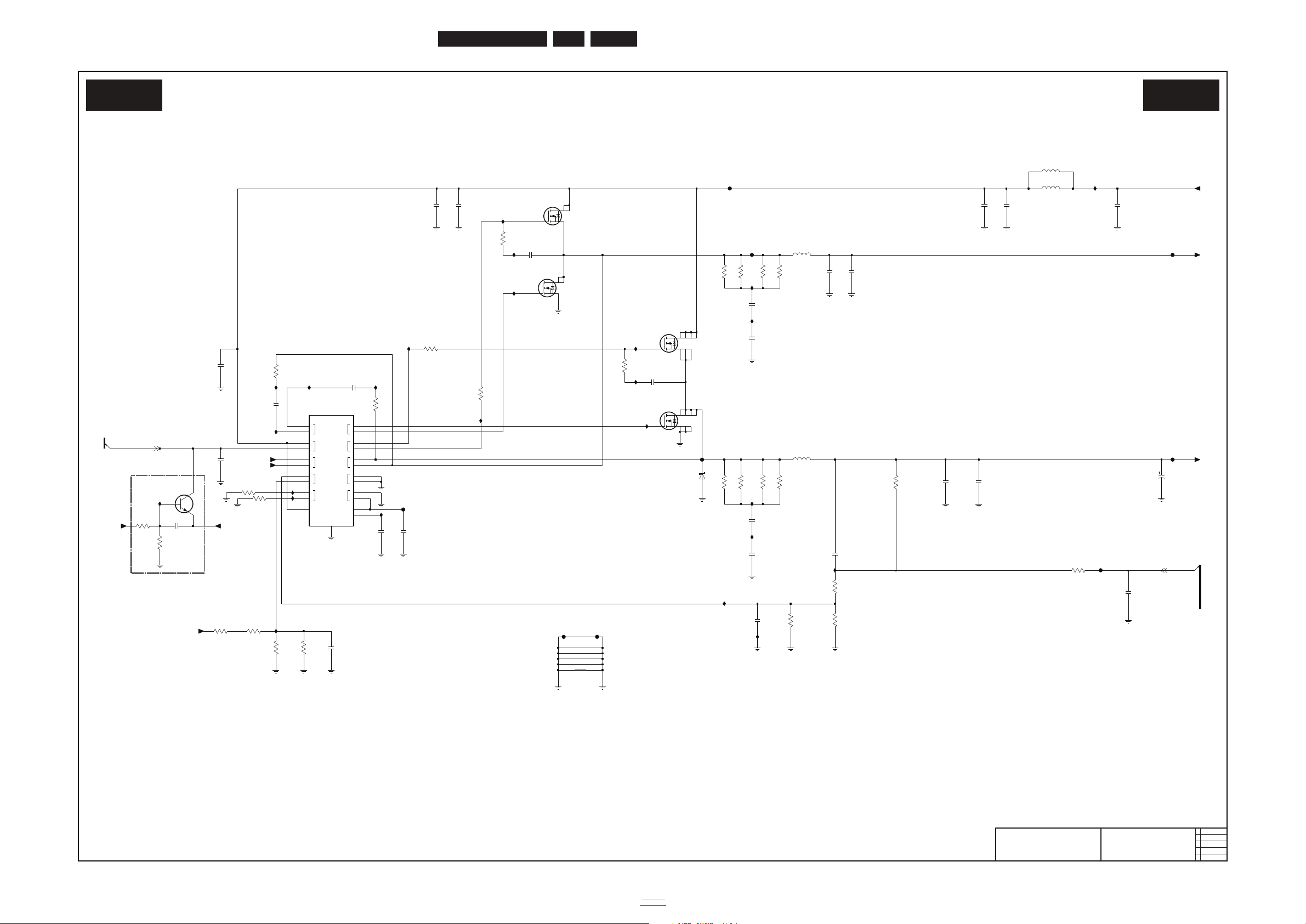
EN 94Q552.2L LA 10.
Circuit Diagrams and PWB Layouts
2011-Jul-15
back to
div. table
DC/DC
19110_031_110415.eps
110415
DC/DC
B03B B03B
2011-03-09
3
2010-12-23
2
3139 123 65213
SPB SSB TV550
2K11 4DDR BR SD
2
VFB
1
2
TRIP
DRVL
1
2
DRVH
1
2
SW
1
2
PGND
1
2
TEST
1
2
VREG5
V5FILT
1
2
VIN
GND
VBST
1
2
EN
1
2
VO
1
12V/1V1 CONVERSION
*
0402 Jumper
RES
12V/1V8 CONVERSION
IU06
FU04
3U04
3R3
IU18
IU19
IU15
GND-SIG
IU21
2U10
1u0
47R
3U24-2
IU20
FU06
IU04
FU05
100n
2U01
3U28
10R
IU10
1u0
2U20
IU14
IU12
RES
GND-SIG
2U03
1n0
3R3
3U05
56
4
3
+12V
7U02-2
SI4952DY
CU04
CU05
CU00
GND-SIG
RES
IU16
2U29
100n
22u
2U16
+1V1
GND-SIG
FU01
3U03
12K
10u
2U19
3U01
10K
10R
CU01
3U27
RES
2U21
220p
100p
2U08
IU05
1%
FU08
10R
RES
3U21
100R
3U20
2U09
1n0
GND-SIG
2U11
1n0
1n0
2U18
GND-SIG
678
4
123
SI4778DY
7U01
5
47R
3U23-4
45
RES
IU22
2U14
100u 2.0V
GND-SIG
IU11
+3V3-STANDBY
2U02
100n
IU23
IU17
IU01
IU24
GND-SIG
IU08
IU13
+1V8
1%
+1V1
FU02
3U22
1K0
GND-SIG
GND-SIG
+1V1
220p
2U22
FU09
FU03
IU07
2U00
+1V8
10u
IU09
2U04
10u
1%
GND-SIG
1
3
2
3U08
330R
7U00
BC847BW
IU25
3U24-1
47R
CU03
CU02
2U17
1n0
2U12
47u
3U24-3
47R
3U24-4
47R
18
47R
27
3U23-1
47R
3U23-2
47u
2U15
6
5U01
2u0
3U23-3
47R
3
22K
3U02
10u
2U24
2U25
10u
3R3
3U11
RES
5U02
30R
FU00
5U03
30R
8
20
4
9
19
24
13
7
17
21
16
18
2
11
5
1
12
23
14
3
10
6
22
15
123
7U03
TPS53126PW
7U04
SI4778DY
5678
4
5U00
3u6
GND-SIG
GND-SIG
STPS2L30A
2U05
1u0
6U00
2U23
10u
78
2
1
22u
2U13
SI4952DY
7U02-1
3U17
330R
1%
22K
3U10
100p
2U07
RES
1K0
3U09
1%
1K0
3U18
1%
5K6
3U19
10K
IU03
+1V8
3U00
2U06
100n
3U14
3R3
IU02
ENABLE-1V8
SENSE+1V1
Page 95
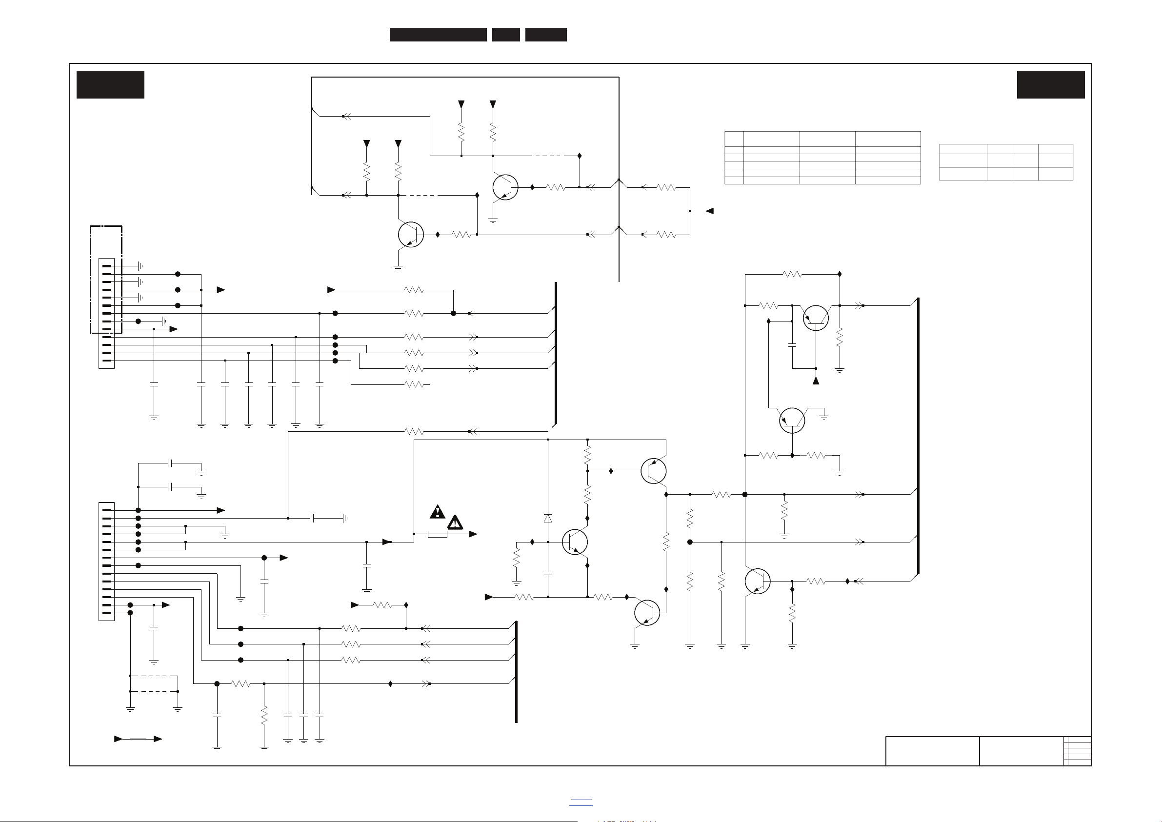
Circuit Diagrams and PWB Layouts
EN 95Q552.2L LA 10.
2011-Jul-15
back to
div. table
DC/DC
19110_032_110415.eps
110415
DC/DC
B03C B03C
2011-03-09
3
2010-12-23
2
3139 123 6521
SPB SSB TV550
2K11 4DDR BR SD
Emmy Sundance / Infinity
BlockBuster
( +12V AL)
4U01
yes
no
no
)stes thgilbmA-non roF()LA V42+ (
4U00
yes
**
**
optionally 1M99 is a 9 pin connector
no
yes
yes
yes
no no
MAINS-OK
yes
yes
no
no
Items
2U56
no
**
Optional table for Ambilight
Optional table for Styling
**
1M99
1M95
open
100p
3U432U44
Core Range
**
14 POLE
100R
*
*
13 POLE
0RDream Catcher
1M95
IU43
3U44
+3V3-STANDBY
+3V3
GND_AL
RES 100R
2
6
1
5
3
4
7U48-1
BC857BS(COL)
7U48-2
BC857BS(COL)
IU55
FU55
FU63
FU61
10K
3U81
10K
3U68
IU40
3U83-1
18
+3V3-STANDBY
100K
+12VIN
FU53
2U51
+12VD
27
RES
100p
10K
3U62-2
9U41
IU62
IU50
3U73
3K3
FU52
RES 2U43 100p
IU57
1n0
2U56
10K
18
3U62-1
2U49
100n
IU41
6
10n2U46
100K
3U83-3
3
3U82
1K0 RES
RES
+5V
3U63
10K
3U60-1
81
GND_AL
+3V3-STANDBY
22K
100p2U44
FU07
3U59
10K RES
IU64
FU74
3U66 100R
RES
+24V
FU49
4
IU48
BC847BPN(COL)
7U40-2
5
3
BC847BPN(COL)
2
6
1
4K7
7U40-1
3U80
+12VIN
2U54
10n
FU62
+3V3
100R
RES
3U53
10K
3U84
FU50
3U64
1K0
IU56
22K
3U60-4
45
4U00
72
22K
3U60-2
RES
IU63
9U42
BC847BW
7U43
RES
1n0
2U57
BZX384-C6V2
6U40
1u0
2U68
36
FU58
45
10K
3U62-3
3U62-4
10K
2U45
FU76
1n0
FU56
100K
4U01
3U65
+3V3-STANDBY
3U74
10K
RES
+24V-AUDIO-POWER
FU57
FU48
GND-AUDIO
100K
45
100n
2U71
3U83-4
10K
3U41
RES
IU45
3U61
10K
RES
+12VIN
2U48 100p
RES
+3V3-STANDBY
10n
2U47
3U76
100R
2U72
RES
FU68
RES 100p
IU61
FU60
IU49
100R
3U43
7
8
9
+3V3
1
10
11
12
13
2
3
4
5
6
1-2041145-3
1M99
FU67
3U42
FU66
100R
100R
3U45
RES
FU77
100R
3U67
2U50
10n
FU51
2U52
RES 100p
FU59
5
6
7
8
9
+12V_AL
1
10
11
12
13
14
2
3
4
1M95
1-2041145-4
2U58
100n
+3V3
FU54
IU51
100R3U71
FU75
1n0
RES
2U53
6
1
1u0
2U55
BC847BS(COL)
7U41-1
2
IU52
FU73
IU44
10K
3U75
RES
IU47
10K
10K
3U70
RES 3U56
36
FU72
3U60-3
22K
3
4
GND_AL
7U41-2
BC847BS(COL)
5
BC847BW
RES
GND_AL
7U42
3U69
10K
RES
1U40
3.0A 32VT
1K0
3U72
27
+12V
3D-LR
100K
3U83-2
LAMP-ON
BACKLIGHT-PWM_BL-VS
BACKLIGHT-BOOST
POWER-OK
BL-SPI-SDO
BL-SPI-CSn
ENABLE-1V8
ENABLE-3V3n
ENABLE-3V3-5V
BL-SPI-CLK
LED-1
LED1
LED-2
LED2 LED2
LED1
STANDBY
DETECT2
***
***
***
***
Page 96
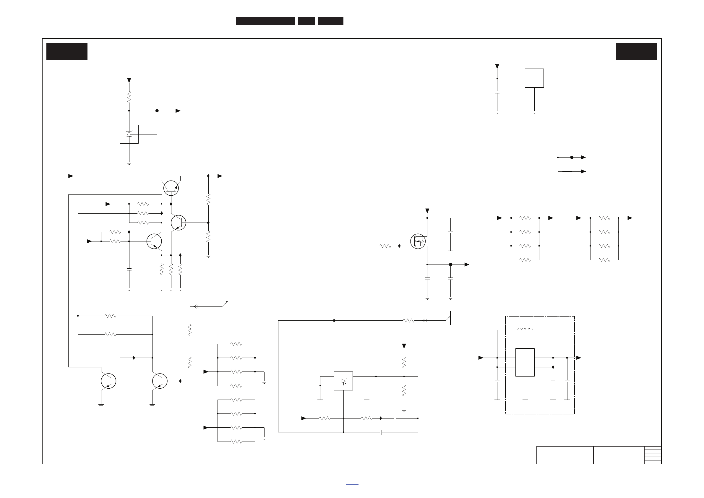
EN 96Q552.2L LA 10.
Circuit Diagrams and PWB Layouts
2011-Jul-15
back to
div. table
DC/DC
19110_033_110415.eps
110415
DC/DC
B03D B03D
2011-03-09
3
2010-12-23
2
3139 123 6521
SPB SSB TV550
2K11 4DDR BR SD
OUTIN
INH BP
COM
COM
OUTIN
NCNC
A
REF
K
*
*
NOT FOR 5000 SERIES
*
RESERVED
*
*
RES
36
RES
27
470R
3U26-3
18
3U26-2
470R
470R
3U26-1 RES
IUB6
22R
3UB0
12
IUA5
7UA3
PHD38N02LT
2K2
3UA0
3
AK
1
R
2
+12V
7UA0
TS2431
+2V5-REF
FUA0
3U16-3
36
27
100R
18
100R
3U16-2
100R
3U16-1
+5V
100n
2UB5
7
5UA0
30R
3U15-2
100R
2
3U15-1
100R
18
IU26
RES
18
+1V8
+3V3
3U29-1
470R
22u
2UB8
1u0
2UB0
2UA4
1u0
470R
3U29-2
RES
27
CUA0
5
3U26-4
470R
RES
4
3U25-1
RES
81
100K RES
27
100K
+2V5
3U25-2
RES
45
+3V3
6
470R
3U29-4
3U29-3
470R
RES
3
100K
3U25-3
RES
36
7UA7-1
BC847BS(COL)
2
6
1
18
7UA6
BC817-25W
3UB6-1
1K0
1K0
3UB6-2
27
3UB6-3
1K0
36
+3V3
+5V-TUN
+12V
3U15-4
100R
45
100R
36
+2V5-LVDS
3U15-3
3U13
330R
1%
FUA4
+2V5-REF
7UC0
LF25ABDT
2
13
4
2
1
3
5
+5V5-TUN
7UA5
LDS3985M50
+12V
+5V-TUN
1u0
2UB6
3UB2
4K7
4K7
3UB3
45
+3V3
+5V
100R
3U16-4
IU29
+5V
7U06-2
BC847BS(COL)
RES
5
3
4
7U06-1
RES
2
6
1
RES
45
BC847BS(COL)
3U25-4
100K
IUB1
+3V3
+1V2
2UB7
1u0
3UB1
1K0
IUB0
2UB3
1n0
2UB4
330p
RES
1K0
3UB4
IUA6
FUA3
RES
2UB1
1u0
1u0
2UB2
5
3
4
IUB4
BC847BS(COL)
7UA7-2
IUB3
IUB2
81
470R
63
470R
3UB7-1
3UB7-3
100K
3UB5
TS431AILT
7UA4
53
12
4
72
+5V5-TUN
4
470R
3UB7-2
3UB7-4
470R
5
3UB6-4
45
330R
1%
1K0
3U12
IUB5
IU30
ENABLE-1V8
SENSE+1V2
Page 97
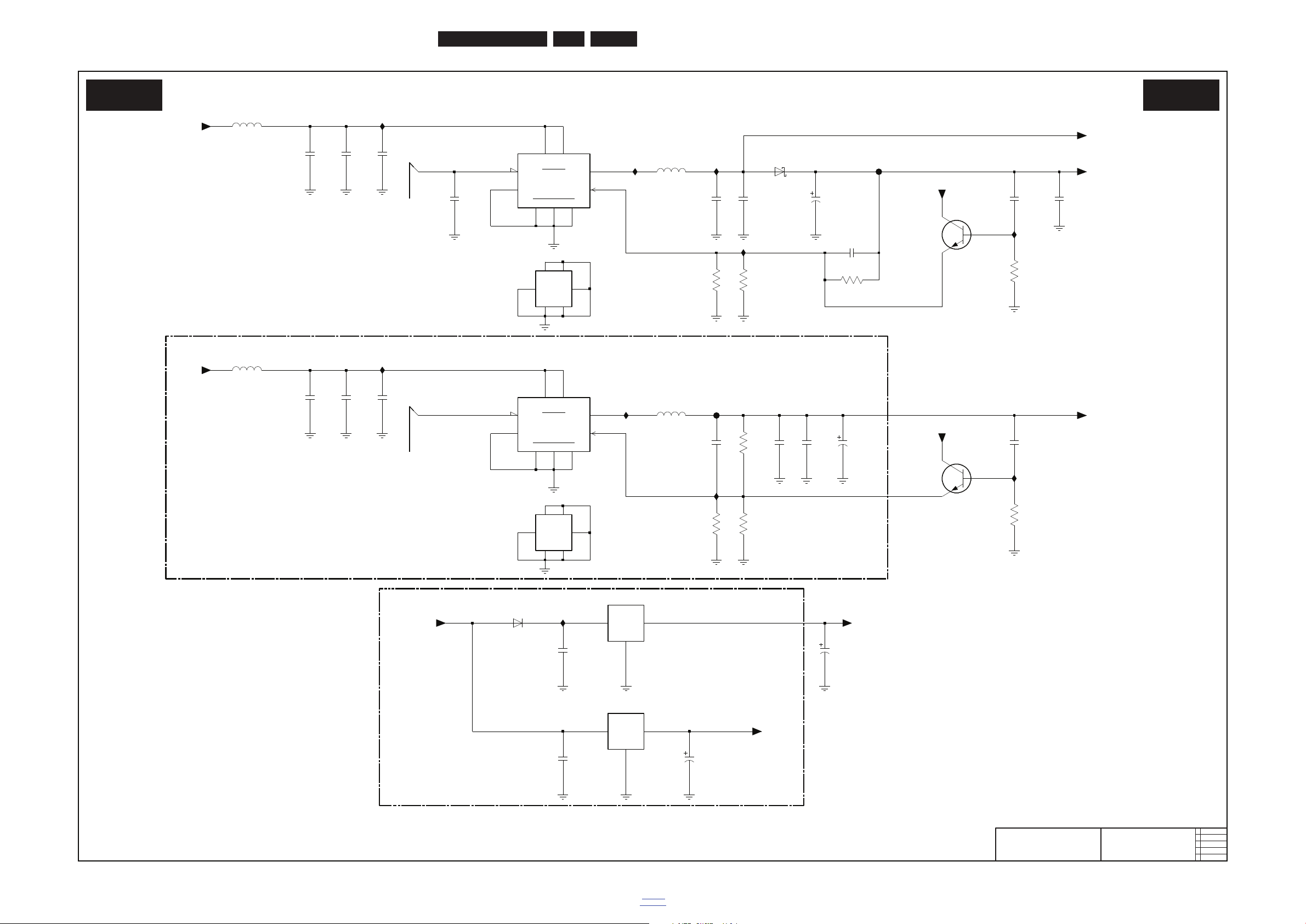
Circuit Diagrams and PWB Layouts
EN 97Q552.2L LA 10.
2011-Jul-15
back to
div. table
DC/DC
19110_034_110415.eps
110415
DC/DC
B03E B03E
2011-03-09
3
2010-12-23
2
3139 123 6521
SPB SSB TV550
2K11 4DDR BR SD
GND
VIN
HSPA
INH
SYNC
SW
VFB
A
SW
VIA
VIA
GND
VIN
HSPA
INH
SYNC
SW
VFB
A
SW
COM
OUTIN
COM
OUTIN
*
0402 Jumper
*
0402 Jumper
FOR 5000 SERIES ONLY
**
(*)
NOT FOR 5000 SERIES
(**)
*
7
35
1
6
ST1S10PH
7UD1-1
4
9
2
8
2
6
1
+1V1
RES
BC847BS(COL)
7U05-1
3UD0
68K
1%
3UD3
100K1%
S1D
6UD1
IUD1
IUD2
10
11
12
13
14 15
+12V
ST1S10PH
7UD0-2
IUD5
4n7
2UD7
IUD6
+2V5
10u
2UD2
4n7
2UE1
1%
3UD5
33K
5UD0
30R
IUD7
2UD1
10u
10u
2UD0
22u
2UE9
2U27
100n
RES
RES
16V22u
2UE6
+5V
+3V3
+12V
IU27
IUD3
IUD4
100n
2UE5
RES
100n
2U28
2UE3
22u
22u
2UE2
7U05-2
5
3
4
8
7
35
1
6
RES
BC847BS(COL)
7UD0-1
ST1S10PH
4
9
2
3UD4
1M0
IUD0
+3V3
1%
6UD0
SS36
33K
3UD1
IU28
FUD2
2UD8
10u
22u
2UD4
3u6
12
13
14 15
5UD1
7UD1-2
ST1S10PH
10
11
2UE8
22u 16V
10K
3U07
+5V
RES
32
+1V1
7UD2
LD1117DT25
1
2UE7
100n
120K
3UD2
220u 16V
2UE4
2UE0
10u
10u
2UD9
FUD3
+5V5-TUN
16V220u
2UD6
RES
1n0
2UD3
30R
5UD3
1
32
7UD3
LD1117DT33
3U06
10K
RES
2UD5
22u
3u6
5UD2
ENABLE-3V3-5V
ENABLE-3V3-5V
Page 98
EN 98Q552.2L LA 10.
Circuit Diagrams and PWB Layouts
2011-Jul-15
back to
div. table
Temperature sensor & AmbiLight
19110_035_110415.eps
110415
Temperature sensor & AmbiLight
B03F B03F
2011-03-09
3
2010-12-23
2
3139 123 65213
SPB SSB TV550
2K11 4DDR BR SD
FUM0
5UM1
A0.1R03
1UM0
T 63V
+3V3
V-AMBI
IUM0
Page 99
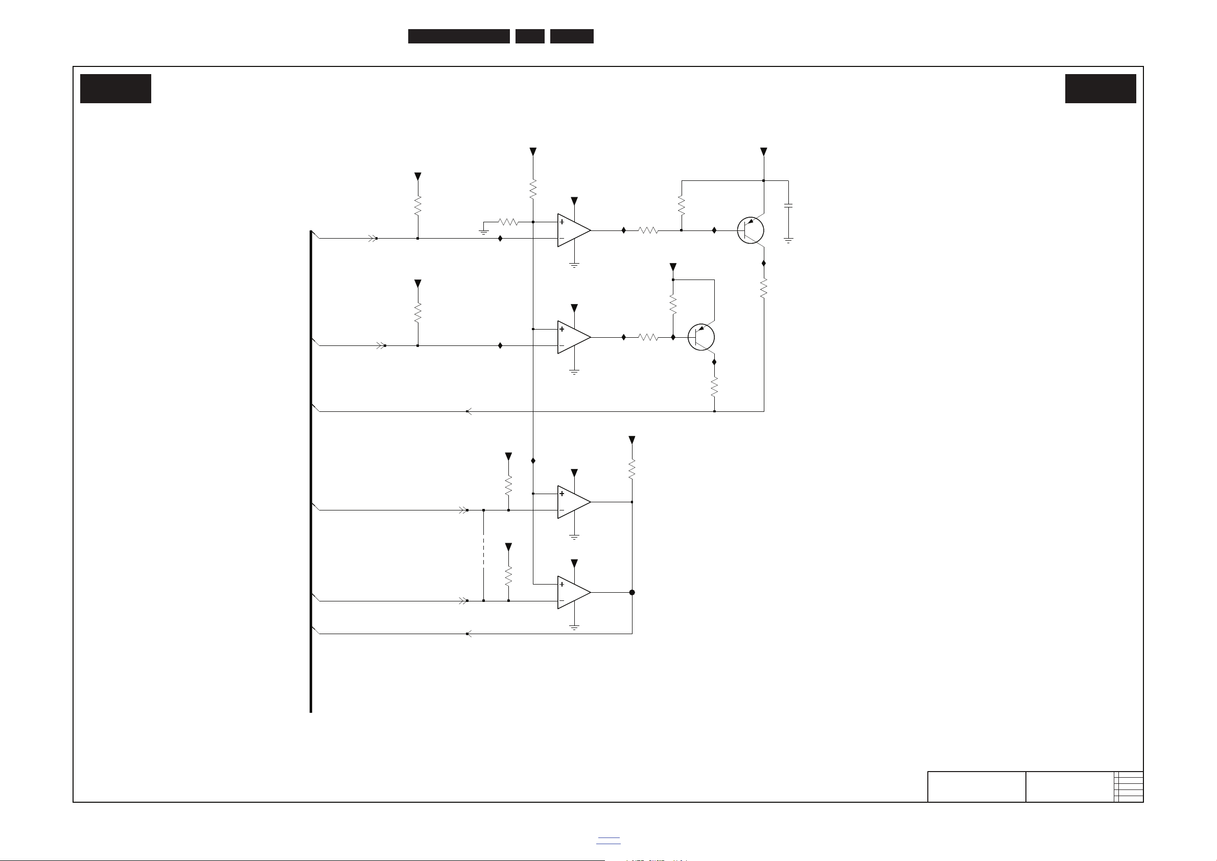
Circuit Diagrams and PWB Layouts
EN 99Q552.2L LA 10.
2011-Jul-15
back to
div. table
Fan control
19110_035_110415.eps
110415
Fan control
B03G B03G
2011-03-09
3
2010-12-23
2
3139 123 6521
SPB SSB TV550
2K11 4DDR BR SD
+12V
+12V
3US4-2
27
+12V
11
10
13
3
12
10K
14
3
12
7US1-2
LM339P
LM339P
7US1-1
9
8
7US1-4
LM339P
7
6
1
312
5
4
2
312
+12V
LM339P
7US1-3
10K
3US4-1
18
3US4-4
10K
45
36
10K
3US4-3
54
3US7
1K0
10K
3US5-4
63
+12V
+12V
3US5-3
10K
3US6
47R
3US9
22R
BC807-25W
7US3
27
7US2
BC807-25W
81
3US5-2
10K
10K
3US5-1
9US0
RES
FUS0
+3V3
+3V3
10K
3US3
3US2
10K
IUT2
IUS9
+3V3
IUT1
IUS8
IUS7
IUS3
IUS5
IUS6
IUS4
+12V
+12V
2US3
100n
FAN-CTRL2
+12V
TACH01
TACH02
TACHO
FAN-CTRL1
FAN-DRV
Page 100
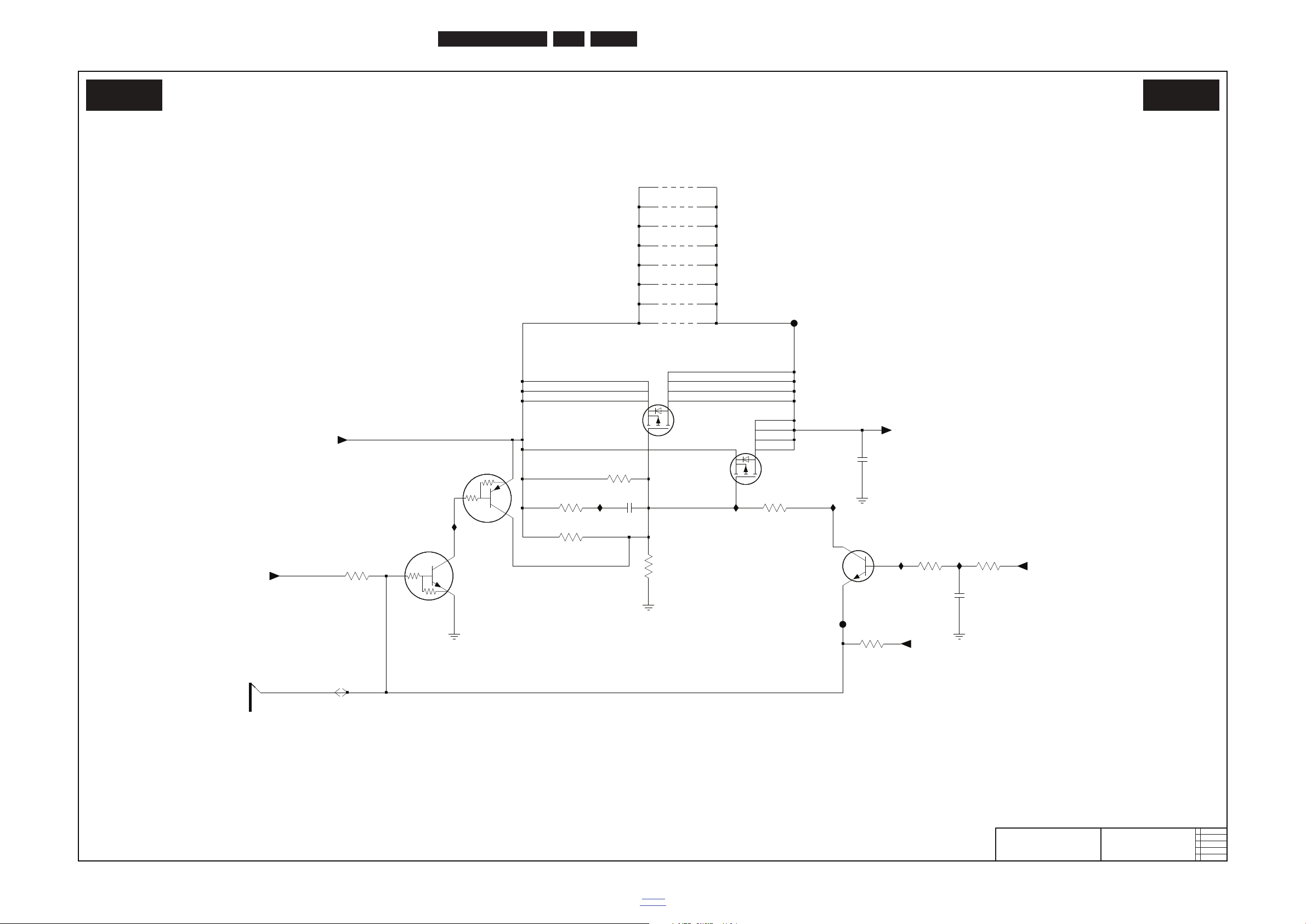
EN 100Q552.2L LA 10.
Circuit Diagrams and PWB Layouts
2011-Jul-15
back to
div. table
Vdisp switch
19110_037_110415.eps
110415
Vdisp switch
B03H B03H
2011-03-09
3
2010-12-23
2
3139 123 6521
SPB SSB TV550
2K11 4DDR BR SD
VDISP-SWITCH
IUU3
FUU0
IUU4
9UU1-118
9UU1-227
RES
RES
9UU1-336
RES
RES
9UU0-4
45
22n
2UU2RES
1
3
2
45
RES
BC847BW
7UU3
RES47K
3UU3-4
RES
9UU0-1
18
RES
7UU0
SI4835DDY
RES
3UU2
4K7
47K
3UU3-2
27
RES
+3V3-STANDBY
+VDISP-INT
+3V3
9UU1-445
IUU1
RES
SI3441BDV
FUU1
7UU1
RES
RES
72
RES
81
47K
3UU0-2
81
47K
3UU0-1
RES
3UU3-1
47K
IUU0
63
+3V3
RES
3UU3-3
47K
9UU0-3
36
+12VD
9UU0-2
27
RES
RES
5
3
4
RES
RES
2
6
1
7UU2-2
PUMD12
RES
45
PUMD12
7UU2-1
47K
3UU0-4
IUU5
IUU2
1u0
2UU1RES
RES 3UU1
47R
RES
100n
2UU0
LCD-PWR-ONn
 Loading...