

Page 1
Colour Television Chassis
TPM15.1E
LA
Contents Page Contents Page
1. Revision List 2
2. Technical Specs, Diversity, and Connections 2
3. Precautions, Notes, and Abbreviation List 5
4. Mechanical Instructions 9
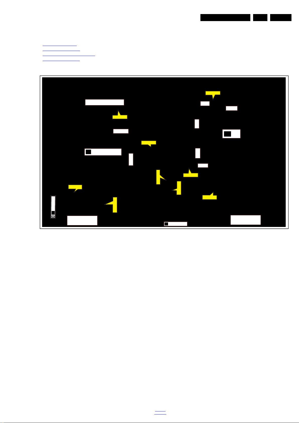
Cable dressing (32" 5300 series) 9
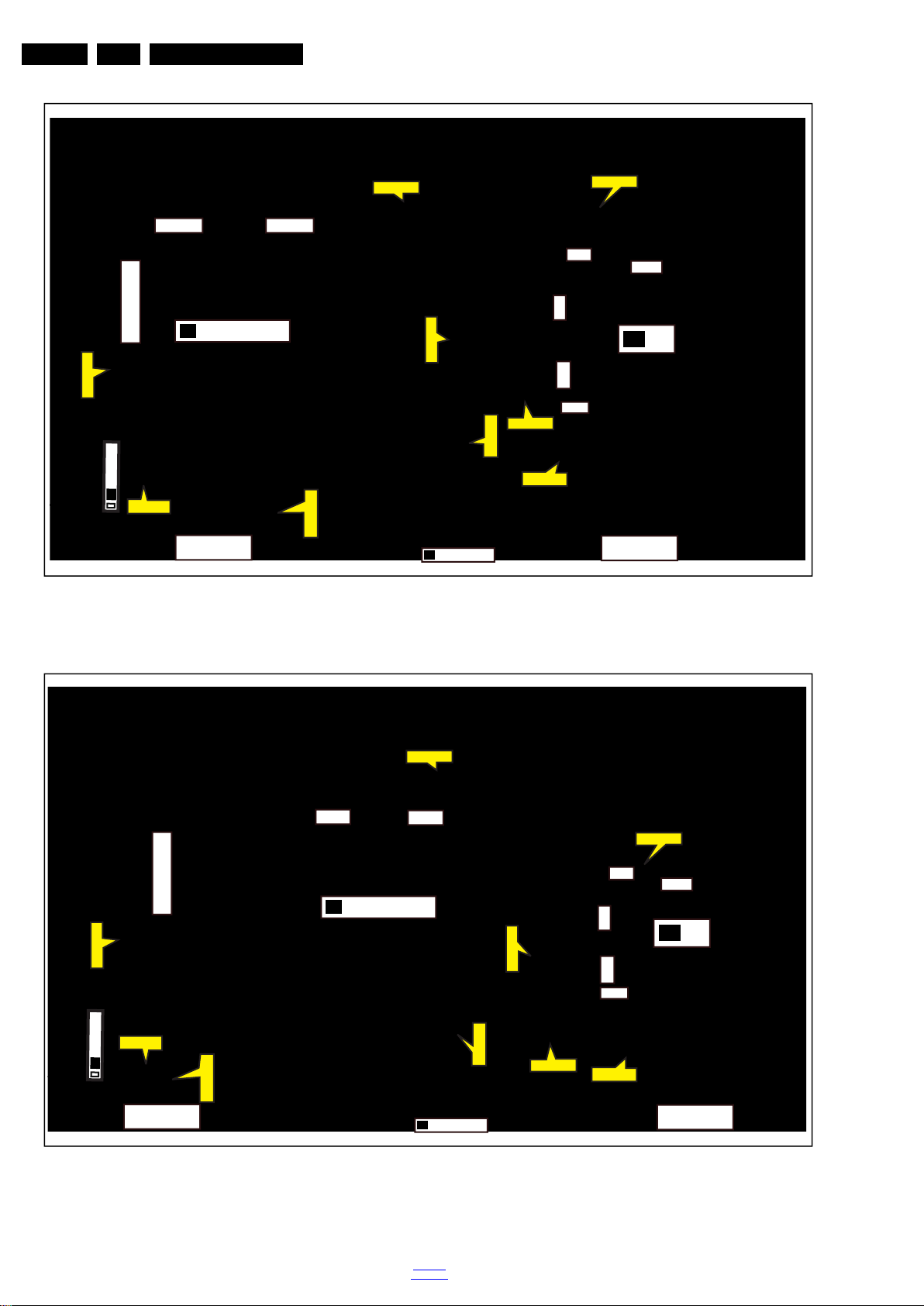
Cable dressing (40" 5300 series) 10
Cable dressing (50" 5300 series) 10
5. Service Modes, Error Codes, and Fault Finding 13
6. Alignments 21
7. Circuit Descriptions 24
8. IC Data Sheets 29
9. Block Diagrams
Block diagram 5300 series 37
10. Circuit Diagrams and PWB Layouts Drawing PWB
A 715G6550 PSU
A 715G6353 PSU 42 46-47
A 715G6338 PSU 48 53-54
B 715G6165 SSB 55 69-70
J 715G6167 IR/LED Panel 71 72
E 715G6316 Keyboard control panel 73 74
11. Styling Sheets
5300 series 32" 75
5300 series 40" 76
5300 series 50" 77
38 40-41
Published by CQZ/SC 1524 Quality Printed in the Netherlands Subject to modification EN 3122 785 19781
2015-Jun-12
2015 ©
TP Vision Netherlands B.V.
All rights reserved. Specifications are subject to change without notice. Trademarks are the
property of Koninklijke Philips Electronics N.V. or their respective owners.
TP Vision Netherlands B.V. reserves the right to change products at any time without being obliged to adjust
earlier supplies accordingly.
PHILIPS and the PHILIPS’ Shield Emblem are used under license from Koninklijke Phili ps Electronics N.V.
Page 2
EN 2 TPM15.1E LA1.
Revision List
1. Revision List
Manual xxxx xxx xxxx.0
• First release.
Manual xxxx xxx xxxx.1
• Chapter 6: Updated tables 6-3 Display code overview
2. Technical Specs, Diversity, and Connections
.
Index of this chapter:
• Specifications are indicative (subject to change).
2.1 Technical Specifications
2.2 Directions for Use
2.3 Connections
2.4 Chassis Overview
2.1 Technical Specifications
For on-line product support please use the links in back to
div.table 2-1. Here is product information available, as well as
getting started, user manuals, frequently asked questions and
Notes:
software & drivers.
• Figures can deviate due to the different set executions.
Table 2-1 Described Model Numbers and Diversity
24 910 11
CTN
32PFH5300/88 2-1 4-1 4-4 4-5 9.1 10.1 10.4 10.5 10.6 11.1
32PFK5300/12 2-1 4-1 4-4 4-5 9.1 10.1 10.4 10.5 10.6 11.1
32PFT5300/12 2-1 4-1 4-4 4-5 9.1 10.1 10.4 10.5 10.6 11.1
32PFT5300/60 2-1 4-1 4-4 4-5 9.1 10.1 10.4 10.5 10.6 11.1
40PFH5300/88 2-1 4-2 4-4 4-5 9.1 10.2 10.4 10.5 10.6 11.2
40PFK5300/12 2-1 4-2 4-4 4-5 9.1 10.2 10.4 10.5 10.6 11.2
40PFT5300/12 2-1 4-2 4-4 4-5 9.1 10.2 10.4 10.5 10.6 11.2
40PFT5300/60 2-1 4-2 4-4 4-5 9.1 10.2 10.4 10.5 10.6 11.2
50PFH5300/88 2-1 4-3 4-4 4-5 9.1 10.3 10.4 10.5 10.6 11.3
50PFK5300/12 2-1 4-3 4-4 4-5 9.1 10.3 10.4 10.5 10.6 11.3
50PFT5300/12 2-1 4-3 4-4 4-5 9.1 10.3 10.4 10.5 10.6 11.3
50PFT5300/60 2-1 4-3 4-4 4-5 9.1 10.3 10.4 10.5 10.6 11.3
Mechanics
Connection Overview
Wire Dressing
Rear Cover Removal
Schematics
SSB Removal
Block Diagram
Power Supply
SSB
J (IR/LED)
E (Key board/Leading Edge)
Styling
2.2 Directions for Use
Directions for use can be downloaded from the following
websites:
http://www.philips.com/support
http://www.p4c.philips.com
2015-Jun-12
back to
div.table
Page 3
2.3 Connections
HDMI ARC
USB
1
USB
2
CI
NETWORK
TV ANTENNA
SERV.U
AUDIO IN DVI
SCART
(RGB/CVBS)
(Optional)
R L
CVBS/Y Pb
Pr
DIGITAL
AUDIO OUT
SAT
HDMI 1
ARC
19780_001.eps
1
2
3
4
5
78
9
6
10
12
11
14
13
Side ConnectorsRear Connectors
1 2 3 4
10000_022_090121.eps
090121
10000_017_090121.eps
090428
19
1
18 2
1 2 3 4
10000_022_090121.eps
090121
Technical Specs, Diversity, and Connections
EN 3TPM15.1E LA 2.
2.3.1 Side Connections
Figure 2-1 Connection overview
Note: The following connector colour abbreviations are used
(acc. to DIN/IEC 757): Bk= Black, Bu= Blue, Gn= Green,
Gy= Grey, Rd= Red, Wh= White, Ye= Yellow.
1 - Common Interface
68p- See figure 10-4-11
jk
2 - USB2 2.0
Figure 2-2 USB (type A)
1-+5V k
2 -Data (-) jk
3 -Data (+) jk
4 -Ground Gnd H
3 - HDMI: Digital Video - In, Digital Audio with ARC - In/Out
Figure 2-3 HDMI (type A) connector
1 -D2+ Data channel j
2-Shield Gnd H
3 -D2- Data channel j
4 -D1+ Data channel j
5-Shield Gnd H
6 -D1- Data channel j
7 -D0+ Data channel j
8 -Shield Gnd H
9 -D0- Data channel j
10 - CLK+ Data channel j
11 - Shield Gnd H
12 - CLK- Data channel j
13 - Easylink/CEC Control channel jk
14 - ARC Audio Return Channel k
15 - DDC_SCL DDC clock j
16 - DDC_SDA DDC data jk
17 - Ground Gnd H
18 - +5V j
19 - HPD Hot Plug Detect j
20 - Ground Gnd H
4 - USB1 2.0
1-+5V k
2 -Data (-) jk
3 -Data (+) jk
4 -Ground Gnd H
5 - Head phone (Output)
Bk -Head phone 80 - 600 / 10 mW ot
2.3.2 Rear Connections
6 - SAT - In
Signal input from an SAT.
back to
div.table
Figure 2-4 USB (type A)
2015-Jun-12
Page 4
EN 4 TPM15.1E LA2.
10000_017_090121.eps
090428
19
1
18 2
10000_025_090121.eps
120320
Technical Specs, Diversity, and Connections
7 - TV ANTENNA - In
Signal input from an antenna, cable or satellite.
8 - Audio - In: Left / Right, VGA
Gn - Audio L/R in 0.5 V
/ 10 kW jq
RMS
9 - HDMI 2: Digital Video - In, Digital Audio with ARC In/Out
Figure 2-5 HDMI (type A) connector
1 -D2+ Data channel j
2-Shield Gnd H
3 -D2- Data channel j
4 -D1+ Data channel j
5-Shield Gnd H
6 -D1- Data channel j
7 -D0+ Data channel j
8-Shield Gnd H
9 -D0- Data channel j
10 - CLK+ Data channel j
11 - Shield Gnd H
12 - CLK- Data channel j
13 - Easylink/CEC Control channel jk
14 - ARC Audio Return Channel k
15 - DDC_SCL DDC clock j
16 - DDC_SDA DDC data jk
17 - Ground Gnd H
18 - +5V j
19 - HPD Hot Plug Detect j
20 - Ground Gnd H
10 - RJ45: Ethernet
Figure 2-6 Ethernet connector
1 -TD+ Transmit signal k
2 -TD- Transmit signal k
3 -RD+ Receive signal j
4 -CT Centre Tap: DC level fixation
5 -CT Centre Tap: DC level fixation
6 -RD- Receive signal j
7 -GND Gnd H
8 -GND Gnd H
11 - Cinch: Video YPbPr - In, Audio - In
Gn - Video - Y 1 V
Bu -Video - Pb 0.7 V
Rd -Video - Pr 0.7 V
Wh -Audio - L 0.5 V
Rd -Audio - R 0.5 V
/ 75 W jq
PP
/ 75 W jq
PP
/ 75 W jq
PP
/ 10 kW jq
RMS
/ 10 kW jq
RMS
12 - Cinch: Digital Audio - Out
BK - Coaxial 0.4 - 0.6V
/ 75 W kq
PP
13 - Service / UART
1 -Ground Gnd H
2 -UART_TX Transmit k
3 -UART_RX Receive j
14 - SCART: Video RGB/YC - In, CVBS - In/Out, Audio In/Out
20
21
10000_001_090121.eps
2
1
090121
Figure 2-7 SCART connector
1 -Audio R 0.5 V
2 -Audio R 0.5 V
3 -Audio L 0.5 V
/ 1 k k
RMS
/ 10 k j
RMS
/ 1 k k
RMS
4 -Ground Audio Gnd H
5 -Ground Blue Gnd H
6 -Audio L 0.5 V
7 -Video Blue/C-out 0.7 V
8 -Function Select 0 - 2 V: INT
/ 10 k j
RMS
/ 75 jk
PP
4.5 - 7 V: EXT 16:9
9.5 - 12 V: EXT 4:3 j
9 -Ground Green Gnd H
10 - n.c.
11 - Video Green 0.7 V
12 - n.c.
/ 75 j
PP
13 - Ground Red Gnd H
14 - Ground P50 Gnd H
15 - Video Red/C 0.7 V
16 - Status/FBL 0 - 0.4 V: INT
/ 75 j
PP
1 - 3 V: EXT / 75 j
17 - Ground Video Gnd H
18 - Ground FBL Gnd H
19 - Video CVBS 1 V
20 - Video CVBS/Y 1 V
21 - Shield Gnd H
/ 75 k
PP
/ 75 j
PP
2.4 Chassis Overview
Refer to 9. Block Diagrams for PWB/CBA locations.
2015-Jun-12
back to
div.table
Page 5

Precautions, Notes, and Abbreviation List
3. Precautions, Notes, and Abbreviation List
Index of this chapter:
3.1 Safety Instructions
3.2 Warnings
3.3 Notes
3.4 Abbreviation List
3.1 Safety Instructions
Safety regulations require the following during a repair:
• Connect the set to the Mains/AC Power via an isolation
transformer (> 800 VA).
• Replace safety components, indicated by the symbol h,
only by components identical to the original ones. Any
other component substitution (other than original type) may
increase risk of fire or electrical shock hazard.
Safety regulations require that after a repair, the set must be
returned in its original condition. Pay in particular attention to
the following points:
• Route the wire trees correctly and fix them with the
mounted cable clamps.
• Check the insulation of the Mains/AC Power lead for
external damage.
• Check the strain relief of the Mains/AC Power cord for
proper function.
• Check the electrical DC resistance between the Mains/AC
Power plug and the secondary side (only for sets that have
a Mains/AC Power isolated power supply):
1. Unplug the Mains/AC Power cord and connect a wire
between the two pins of the Mains/AC Power plug.
2. Set the Mains/AC Power switch to the “on” position
(keep the Mains/AC Power cord unplugged!).
3. Measure the resistance value between the pins of the
Mains/AC Power plug and the metal shielding of the
tuner or the aerial connection on the set. The reading
should be between 4.5 M and 12 M.
4. Switch “off” the set, and remove the wire between the
two pins of the Mains/AC Power plug.
• Check the cabinet for defects, to prevent touching of any
inner parts by the customer.
3.2 Warnings
• All ICs and many other semiconductors are susceptible to
electrostatic discharges (ESD w). Careless handling
during repair can reduce life drastically. Make sure that,
during repair, you are connected with the same potential as
the mass of the set by a wristband with resistance. Keep
components and tools also at this same potential.
• Be careful during measurements in the high voltage
section.
• Never replace modules or other components while the unit
is switched “on”.
• When you align the set, use plastic rather than metal tools.
This will prevent any short circuits and the danger of a
circuit becoming unstable.
3.3 Notes
3.3.1 General
• Measure the voltages and waveforms with regard to the
chassis (= tuner) ground (H), or hot ground (I), depending
on the tested area of circuitry. The voltages and waveforms
shown in the diagrams are indicative. Measure them in the
Service Default Mode with a colour bar signal and stereo
sound (L: 3 kHz, R: 1 kHz unless stated otherwise) and
picture carrier at 475.25 MHz for PAL, or 61.25 MHz for
NTSC (channel 3).
• Where necessary, measure the waveforms and voltages
with (D) and without (E) aerial signal. Measure the
voltages in the power supply section both in normal
operation (G) and in stand-by (F). These values are
indicated by means of the appropriate symbols.
3.3.2 Schematic Notes
• All resistor values are in ohms, and the value multiplier is
often used to indicate the decimal point location (e.g. 2K2
indicates 2.2 k).
• Resistor values with no multiplier may be indicated with
either an “E” or an “R” (e.g. 220E or 220R indicates 220 ).
• All capacitor values are given in micro-farads (10
nano-farads (n 10
• Capacitor values may also use the value multiplier as the
decimal point indication (e.g. 2p2 indicates 2.2 pF).
• An “asterisk” (*) indicates component usage varies. Refer
to the diversity tables for the correct values.
• The correct component values are listed on the Philips
Spare Parts Web Portal.
3.3.3 Spare Parts
For the latest spare part overview, consult your Philips Spare
Part web portal.
3.3.4 BGA (Ball Grid Array) ICs
Introduction
For more information on how to handle BGA devices, visit this
URL: http://www.atyourservice-magazine.com
“Magazine”, then go to “Repair downloads”. Here you will find
Information on how to deal with BGA-ICs.
BGA Temperature Profiles
For BGA-ICs, you must use the correct temperature-profile.
Where applicable and available, this profile is added to the IC
Data Sheet information section in this manual.
3.3.5 Lead-free Soldering
Due to lead-free technology some rules have to be respected
by the workshop during a repair:
• Use only lead-free soldering tin. If lead-free solder paste is
required, please contact the manufacturer of your soldering
equipment. In general, use of solder paste within
workshops should be avoided because paste is not easy to
store and to handle.
• Use only adequate solder tools applicable for lead-free
soldering tin. The solder tool must be able:
– To reach a solder-tip temperature of at least 400°C.
– To stabilize the adjusted temperature at the solder-tip.
– To exchange solder-tips for different applications.
• Adjust your solder tool so that a temperature of around
360°C - 380°C is reached and stabilized at the solder joint.
Heating time of the solder-joint should not exceed ~ 4 sec.
Avoid temperatures above 400°C, otherwise wear-out of
tips will increase drastically and flux-fluid will be destroyed.
To avoid wear-out of tips, switch “off” unused equipment or
reduce heat.
• Mix of lead-free soldering tin/parts with leaded soldering
tin/parts is possible but PHILIPS recommends strongly to
avoid mixed regimes. If this cannot be avoided, carefully
clear the solder-joint from old tin and re-solder with new tin.
3.3.6 Alternative BOM identification
It should be noted that on the European Service website,
“Alternative BOM” is referred to as “Design variant”.
The third digit in the serial number (example:
AG2B0335000001) indicates the number of the alternative
B.O.M. (Bill Of Materials) that has been used for producing the
specific TV set. In general, it is possible that the same TV
model on the market is produced with e.g. two different types
of displays, coming from two different suppliers. This will then
back to
div.table
-9
), or pico-farads (p 10
. Select
EN 5TPM15.1E LA 3.
-6
),
-12
).
2015-Jun-12
Page 6

EN 6 TPM15.1E LA3.
10000_053_110228.eps
110228
Precautions, Notes, and Abbreviation List
result in sets which have the same CTN (Commercial Type
Number; e.g. 28PW9515/12) but which have a different B.O.M.
number.
By looking at the third digit of the serial number, one can
identify which B.O.M. is used for the TV set he is working with.
If the third digit of the serial number contains the number “1”
(example: AG1B033500001), then the TV set has been
manufactured according to B.O.M. number 1. If the third digit is
a “2” (example: AG2B0335000001), then the set has been
produced according to B.O.M. no. 2. This is important for
ordering the correct spare parts!
For the third digit, the numbers 1...9 and the characters A...Z
can be used, so in total: 9 plus 26= 35 different B.O.M.s can be
indicated by the third digit of the serial number.
Identification: The bottom line of a type plate gives a 14-digit
serial number. Digits 1 and 2 refer to the production centre (e.g.
SN is Lysomice, RJ is Kobierzyce), digit 3 refers to the B.O.M.
code, digit 4 refers to the Service version change code, digits 5
and 6 refer to the production year, and digits 7 and 8 refer to
production week (in example below it is 2010 week 10 / 2010
week 17). The 6 last digits contain the serial number.
Figure 3-1 Serial number (example)
3.3.7 Board Level Repair (BLR) or Component Level Repair (CLR)
If a board is defective, consult your repair procedure to decide
if the board has to be exchanged or if it should be repaired on
component level.
If your repair procedure says the board should be exchanged
completely, do not solder on the defective board. Otherwise, it
cannot be returned to the O.E.M. supplier for back charging!
3.3.8 Practical Service Precautions
• It makes sense to avoid exposure to electrical shock.
While some sources are expected to have a possible
dangerous impact, others of quite high potential are of
limited current and are sometimes held in less regard.
• Always respect voltages. While some may not be
dangerous in themselves, they can cause unexpected
reactions that are best avoided. Before reaching into a
powered TV set, it is best to test the high voltage insulation.
It is easy to do, and is a good service precaution.
3.4 Abbreviation List
0/6/12 SCART switch control signal on A/V
board. 0 = loop through (AUX to TV),
6 = play 16 : 9 format, 12 = play 4 : 3
format
AARA Automatic Aspect Ratio Adaptation:
algorithm that adapts aspect ratio to
remove horizontal black bars; keeps
the original aspect ratio
ACI Automatic Channel Installation:
algorithm that installs TV channels
directly from a cable network by
means of a predefined TXT page
ADC Analogue to Digital Converter
AFC Automatic Frequency Control: control
signal used to tune to the correct
frequency
AGC Automatic Gain Control: algorithm that
controls the video input of the feature
box
AM Amplitude Modulation
AP Asia Pacific
AR Aspect Ratio: 4 by 3 or 16 by 9
ASF Auto Screen Fit: algorithm that adapts
aspect ratio to remove horizontal black
bars without discarding video
information
ATSC Advanced Television Systems
Committee, the digital TV standard in
the USA
ATV See Auto TV
Auto TV A hardware and software control
system that measures picture content,
and adapts image parameters in a
dynamic way
AV External Audio Video
AVC Audio Video Controller
AVIP Audio Video Input Processor
B/G Monochrome TV system. Sound
carrier distance is 5.5 MHz
BDS Business Display Solutions (iTV)
BLR Board-Level Repair
BTSC Broadcast Television Standard
Committee. Multiplex FM stereo sound
system, originating from the USA and
used e.g. in LATAM and AP-NTSC
countries
B-TXT Blue TeleteXT
C Centre channel (audio)
CEC Consumer Electronics Control bus:
remote control bus on HDMI
connections
CL Constant Level: audio output to
connect with an external amplifier
CLR Component Level Repair
ComPair Computer aided rePair
CP Connected Planet / Copy Protection
CSM Customer Service Mode
CTI Color Transient Improvement:
manipulates steepness of chroma
transients
CVBS Composite Video Blanking and
Synchronization
DAC Digital to Analogue Converter
DBE Dynamic Bass Enhancement: extra
low frequency amplification
DCM Data Communication Module. Also
referred to as System Card or
Smartcard (for iTV).
DDC See “E-DDC”
D/K Monochrome TV system. Sound
carrier distance is 6.5 MHz
DFI Dynamic Frame Insertion
DFU Directions For Use: owner's manual
DMR Digital Media Reader: card reader
DMSD Digital Multi Standard Decoding
DNM Digital Natural Motion
2015-Jun-12
back to
div.table
Page 7

Precautions, Notes, and Abbreviation List
EN 7TPM15.1E LA 3.
DNR Digital Noise Reduction: noise
reduction feature of the set
DRAM Dynamic RAM
DRM Digital Rights Management
DSP Digital Signal Processing
DST Dealer Service Tool: special remote
control designed for service
technicians
DTCP Digital Transmission Content
Protection; A protocol for protecting
digital audio/video content that is
traversing a high speed serial bus,
such as IEEE-1394
DVB-C Digital Video Broadcast - Cable
DVB-T Digital Video Broadcast - Terrestrial
DVD Digital Versatile Disc
DVI(-d) Digital Visual Interface (d= digital only)
E-DDC Enhanced Display Data Channel
(VESA standard for communication
channel and display). Using E-DDC,
the video source can read the EDID
information form the display.
EDID Extended Display Identification Data
(VESA standard)
EEPROM Electrically Erasable and
Programmable Read Only Memory
EMI Electro Magnetic Interference
EPG Electronic Program Guide
EPLD Erasable Programmable Logic Device
EU Europe
EXT EXTernal (source), entering the set by
SCART or by cinches (jacks)
FDS Full Dual Screen (same as FDW)
FDW Full Dual Window (same as FDS)
FLASH FLASH memory
FM Field Memory or Frequency
Modulation
FPGA Field-Programmable Gate Array
FTV Flat TeleVision
Gb/s Giga bits per second
G-TXT Green TeleteXT
H H_sync to the module
HD High Definition
HDD Hard Disk Drive
HDCP High-bandwidth Digital Content
Protection: A “key” encoded into the
HDMI/DVI signal that prevents video
data piracy. If a source is HDCP coded
and connected via HDMI/DVI without
the proper HDCP decoding, the
picture is put into a “snow vision” mode
or changed to a low resolution. For
normal content distribution the source
and the display device must be
enabled for HDCP “software key”
decoding.
HDMI High Definition Multimedia Interface
HP HeadPhone
I Monochrome TV system. Sound
2
C Inter IC bus
I
2
I
D Inter IC Data bus
2
S Inter IC Sound bus
I
carrier distance is 6.0 MHz
IF Intermediate Frequency
IR Infra Red
IRQ Interrupt Request
ITU-656 The ITU Radio communication Sector
(ITU-R) is a standards body
subcommittee of the International
Telecommunication Union relating to
radio communication. ITU-656 (a.k.a.
SDI), is a digitized video format used
for broadcast grade video.
Uncompressed digital component or
digital composite signals can be used.
back to
div.table
The SDI signal is self-synchronizing,
uses 8 bit or 10 bit data words, and has
a maximum data rate of 270 Mbit/s,
with a minimum bandwidth of 135
MHz.
iTV Institutional TeleVision; TV sets for
hotels, hospitals etc.
LS Last Status; The settings last chosen
by the customer and read and stored
in RAM or in the NVM. They are called
at start-up of the set to configure it
according to the customer's
preferences
LATAM Latin America
LCD Liquid Crystal Display
LED Light Emitting Diode
L/L' Monochrome TV system. Sound
carrier distance is 6.5 MHz. L' is Band
I, L is all bands except for Band I
LPL LG.Philips LCD (supplier)
LS Loudspeaker
LVDS Low Voltage Differential Signalling
Mbps Mega bits per second
M/N Monochrome TV system. Sound
carrier distance is 4.5 MHz
MHEG Part of a set of international standards
related to the presentation of
multimedia information, standardised
by the Multimedia and Hypermedia
Experts Group. It is commonly used as
a language to describe interactive
television services
MIPS Microprocessor without Interlocked
Pipeline-Stages; A RISC-based
microprocessor
MOP Matrix Output Processor
MOSFET Metal Oxide Silicon Field Effect
Transistor, switching device
MPEG Motion Pictures Experts Group
MPIF Multi Platform InterFace
MUTE MUTE Line
MTV Mainstream TV: TV-mode with
Consumer TV features enabled (iTV)
NC Not Connected
NICAM Near Instantaneous Compounded
Audio Multiplexing. This is a digital
sound system, mainly used in Europe.
NTC Negative Temperature Coefficient,
non-linear resistor
NTSC National Television Standard
Committee. Color system mainly used
in North America and Japan. Color
carrier NTSC M/N= 3.579545 MHz,
NTSC 4.43= 4.433619 MHz (this is a
VCR norm, it is not transmitted off-air)
NVM Non-Volatile Memory: IC containing
TV related data such as alignments
O/C Open Circuit
OSD On Screen Display
OAD Over the Air Download. Method of
software upgrade via RF transmission.
Upgrade software is broadcasted in
TS with TV channels.
OTC On screen display Teletext and
Control; also called Artistic (SAA5800)
P50 Project 50: communication protocol
between TV and peripherals
PAL Phase Alternating Line. Color system
mainly used in West Europe (colour
carrier = 4.433619 MHz) and South
America (colour carrier
PAL M = 3.575612 MHz and
PAL N = 3.582056 MHz)
PCB Printed Circuit Board (same as “PWB”)
PCM Pulse Code Modulation
2015-Jun-12
Page 8

EN 8 TPM15.1E LA3.
Precautions, Notes, and Abbreviation List
PDP Plasma Display Panel
PFC Power Factor Corrector (or
Pre-conditioner)
PIP Picture In Picture
PLL Phase Locked Loop. Used for e.g.
FST tuning systems. The customer
can give directly the desired frequency
POD Point Of Deployment: a removable
CAM module, implementing the CA
system for a host (e.g. a TV-set)
POR Power On Reset, signal to reset the uP
PSDL Power Supply for Direct view LED
backlight with 2D-dimming
PSL Power Supply with integrated LED
drivers
PSLS Power Supply with integrated LED
drivers with added Scanning
functionality
PTC Positive Temperature Coefficient,
non-linear resistor
PWB Printed Wiring Board (same as “PCB”)
PWM Pulse Width Modulation
QRC Quasi Resonant Converter
QTNR Quality Temporal Noise Reduction
QVCP Quality Video Composition Processor
RAM Random Access Memory
RGB Red, Green, and Blue. The primary
color signals for TV. By mixing levels
of R, G, and B, all colors (Y/C) are
reproduced.
RC Remote Control
RC5 / RC6 Signal protocol from the remote
control receiver
RESET RESET signal
ROM Read Only Memory
RSDS Reduced Swing Differential Signalling
data interface
R-TXT Red TeleteXT
SAM Service Alignment Mode
S/C Short Circuit
SCART Syndicat des Constructeurs
d'Appareils Radiorécepteurs et
SCL Serial Clock I
Téléviseurs
SCL-F CLock Signal on Fast I
SD Standard Definition
SDA Serial Data I
SDA-F DAta Signal on Fast I
2
C
2
C bus
2
C
2
C bus
SDI Serial Digital Interface, see “ITU-656”
SDRAM Synchronous DRAM
SECAM SEequence Couleur Avec Mémoire.
Colour system mainly used in France
and East Europe. Colour
carriers = 4.406250 MHz and
4.250000 MHz
SIF Sound Intermediate Frequency
SMPS Switched Mode Power Supply
SoC System on Chip
SOG Sync On Green
SOPS Self Oscillating Power Supply
SPI Serial Peripheral Interface bus; a
4-wire synchronous serial data link
standard
S/PDIF Sony Philips Digital InterFace
SRAM Static RAM
SRP Service Reference Protocol
SSB Small Signal Board
SSC Spread Spectrum Clocking, used to
reduce the effects of EMI
STB Set Top Box
STBY STand-BY
SVGA 800 × 600 (4:3)
SVHS Super Video Home System
SW Software
SWAN Spatial temporal Weighted Averaging
Noise reduction
SXGA 1280 × 1024
TFT Thin Film Transistor
THD Total Harmonic Distortion
TMDS Transmission Minimized Differential
Signalling
TS Transport Stream
TXT TeleteXT
TXT-DW Dual Window with TeleteXT
UI User Interface
uP Microprocessor
UXGA 1600 × 1200 (4:3)
V V-sync to the module
VESA Video Electronics Standards
Association
VGA 640 × 480 (4:3)
VL Variable Level out: processed audio
output toward external amplifier
VSB Vestigial Side Band; modulation
method
WYSIWYR What You See Is What You Record:
record selection that follows main
picture and sound
WXGA 1280 × 768 (15:9)
XTAL Quartz crystal
XGA 1024 × 768 (4:3)
Y Luminance signal
Y/C Luminance (Y) and Chrominance (C)
signal
YPbPr Component video. Luminance and
scaled color difference signals (B-Y
and R-Y)
YUV Component video
2015-Jun-12
back to
div.table
Page 9
4. Mechanical Instructions
19780_100.eps
CN601
CN401
CN700
CN408
CN8602
CN9101
CN4250
MAIN POWER SUPPLY
(1054)
A
SSB
(1053)
B
ECN408
ECN700
ECN601
ECN601
ECN401
ECN401
LOUDSPEAKER
(1184)
LOUDSPEAKER
(1184)
ECN408
ECN4250
ECN4250
IR/LED BOARD
(1056)
J
KEYBOARD CONTROL
(1057)
E
CN01
WIFI Module
(WiFi01)
Index of this chapter:
4.1 Cable Dressing
4.2 Service Positions
4.3 Assembly/Panel Removal
4.4 Set Re-assembly
4.1 Cable Dressing
Mechanical Instructions
Notes:
• Figures below can deviate slightly from the actual situation,
due to the different set executions.
EN 9TPM15.1E LA 4.
Figure 4-1 Cable dressing (32" 5300 series)
back to
div.table
2015-Jun-12
Page 10
EN 10 TPM15.1E LA4.
19780_102.eps
CN601
CN401
CN700
CN408
CN9301
CN8101
CN4250
MAIN POWER SUPPLY
(1054)
A
SSB
(1053)
B
ECN408
ECN700
ECN601
ECN601
ECN401
ECN401
LOUDSPEAKER
(1184)
LOUDSPEAKER
(1184)
ECN408
ECN4250
ECN4250
IR/LED BOARD
(1056)
J
KEYBOARD CONTROL
(1057)
E
CN01
WIFI Module
(WiFi01)
Mechanical Instructions
ECN4250
(1057)
KEYBOARD CONTROL
E
CN01
WIFI Module
(WiFi01)
ECN401
MAIN POWER SUPPLY
A
(1054)
LOUDSPEAKER
(1184)
ECN700
CN9101CN8101
ECN408
ECN601
IR/LED BOARD
J
(1056)
Figure 4-2 Cable dressing (40" 5300 series)
ECN401
ECN4250
ECN601
CN700
CN401
CN601
CN4250
ECN408
LOUDSPEAKER
CN408
B
(1184)
SSB
(1053)
19780_101.eps
2015-Jun-12
Figure 4-3 Cable dressing (50" 5300 series)
back to
div.table
Page 11
Mechanical Instructions
19780_103.eps
2
2
2
2
2
2
2
2
2
2
2
2
2
2
1
1
1
1
3
1
M4 × 10
M3× 6
2
Q3 × 8
3
EN 11TPM15.1E LA 4.
4.2 Service Positions
For easy servicing of a TV set, the set should be put face down
on a soft flat surface, foam buffers or other specific workshop
tools. Ensure that a stable situation is created to perform
measurements and alignments. When using foam bars take
care that these always support the cabinet and never only the
display. Caution: Failure to follow these guidelines can
seriously damage the display!
Ensure that ESD safe measures are taken.
4.3 Assembly/Panel Removal
Instructions below apply to the 40PFH5300/88, but will be
similar for other models.
4.3.1 Rear Cover
Refer to Figure 4-4
Warning: Disconnect the mains power cord before removing
the rear cover.
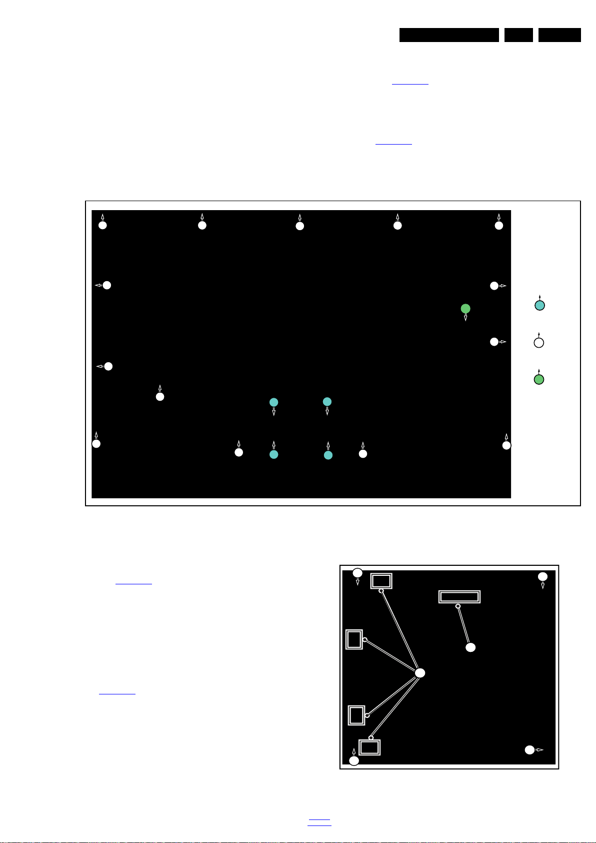
1. Remove fixation screws [1] that secure the base assy, pull
out the base assy from the set. Then remove the fixation
screws [2], [3] that secure the rear cover. Refer to
Figure 4-4
2. Gently lift the rear cover from the TV. Make sure that wires
and cables are not damaged while lifting the rear cover
from the set.
for details.
for details.
4.3.2 Small Signal Board (SSB)
Refer to Figure 4-5
Caution: it is mandatory to remount all different screws at their
original position during re-assembly. Failure to do so may result
in damaging the SSB.
1. Release the clips from the LVDS [1] connector that connect
with the SSB.
Caution: be careful, as these are very fragile connectors!
2. Unplug all other connectors [2].
3. Remove all the fixation screws [3] from the SSB.
4. The SSB can now be shifted from side connector cover,
then lifted and taken out of the I/O bracket.Refer to
Figure 4-5
for details.
for details.
Figure 4-4 Rear cover removal
3
3
2
1
3
back to
div.table
3
Figure 4-5 SSB removal
19780_104.eps
2015-Jun-12
Page 12

EN 12 TPM15.1E LA4.
4.3.3 Power Supply Unit (PSU)
Caution: it is mandatory to remount all different screws at their
original position during re-assembly. Failure to do so may result
in damaging the PSU.
1. Gently unplug all connectors from the PSU.
2. Remove all fixation screws from the PSU.
3. The PSU can be taken out of the set now.
4.3.4 Speakers
1. Gently release the tapes that secures the speaker cables.
2. Unplug the speaker connectors from the SSB.
3. Take the speakers out.
When defective, replace the both units.
4.3.5 Stand bracket
1. Remove all fixation screws of the bracket.
2. Lift the bracket from the set.
4.3.6 Keyboard Control unit
1. Unplug the connector from the keyboard control panel.
2. Remove the fixation screw that secure the keyboard
3. Gently take the keyboard out.
When defective, replace the whole unit.
Mechanical Instructions
4.3.7 IR/LED Board
1. Remove the stand bracket as described earlier.
2. Gently release the clips that hold the board and take it out
from the bezel.
3. Unplug both the connectors from the IR/LED board.
When defective, replace the whole unit.
4.3.8 WIFI module
1. Unplug the connector from the SSB.
2. Remove fixation screw that secure the WIFI module,
getntly remove the module from the set.
When defective, replace the whole unit.
4.3.9 LCD Panel
1. Remove the SSB as described earlier.
2. Remove the PSU as described earlier.
3. Remove the keyboard control panel as described earlier.
4. Remove the stand bracket as described earlier.
5. Remove the IR/LED as described earlier.
6. Remove the WIFI module as described earlier.
7. Remove the fixations screws that fix the metal clamps to
the front bezel. Take out those clamps.
8. Remove all other metal parts not belonging to the panel.
9. Lift the LCD Panel from the bezel.
When defective, replace the whole unit.
4.4 Set Re-assembly
To re-assemble the whole set, execute all processes in reverse
order.
Notes:
• While re-assembling, make sure that all cables are placed
and connected in their original position. See Figure 4-1
Figure 4-3
• Pay special attention not to damage the EMC foams on the
SSB shields. Ensure that EMC foams are mounted
correctly.
2015-Jun-12
.
to
back to
div.table
Page 13

Service Modes, Error Codes, and Fault Finding
5. Service Modes, Error Codes, and Fault Finding
Index of this chapter:
5.1 Test Points
5.2 Service Modes
5.3 Stepwise Start-up
5.4 Service Tools
5.5 Software Upgrading
5.6 Error Codes
5.7 The Blinking LED Procedure
5.8 Fault Finding and Repair Tips
5.1 Test Points
As most signals are digital, it will be difficult to measure
waveforms with a standard oscilloscope. However, several key
ICs are capable of generating test patterns, which can be
controlled via ComPair. In this way it is possible to determine
which part is defective.
Perform measurements under the following conditions:
• Service Default Mode.
• Video: Colour bar signal.
• Audio: 3 kHz left, 1 kHz right.
5.2 Service Modes
The Service Mode feature is split into five parts:
• Service Alignment Mode (SAM).
• Factory Mode.
• Customer Service Mode (CSM).
• Computer Aided Repair Mode (ComPair).
SAM and the Factory mode offer features, which can be used
by the Service engineer to repair/align a TV set. Some features
are:
• Make alignments (e.g. White Tone), reset the error buffer
(SAM and Factory Mode).
• Display information (“SAM” indication in upper right corner
of screen, error buffer, software version, operating hours,
options and option codes, sub menus).
The CSM is a Service Mode that can be enabled by the
consumer. The CSM displays diagnosis information, which the
customer can forward to the dealer or call centre. In CSM
mode, “CSM”, is displayed in the top right corner of the screen.
The information provided in CSM and the purpose of CSM is to:
• Increase the home repair hit rate.
• Decrease the number of nuisance calls.
• Solved customers’ problem without home visit.
ComPair Mode is used for communication between a computer
and a TV on I
engineer to quickly diagnose the TV set by reading out error
codes, read and write in NVMs, communicate with ICs and the
micro processor (PWM, registers, etc.), and by making use of
a fault finding database. It will also be possible to up and
download the software of the TV set via I
ComPair. To do this, ComPair has to be connected to the TV
set via the ComPair connector, which will be accessible
through the rear of the set (without removing the rear cover).
Note: For the new model range, a new remote control (RC) is
used with some renamed buttons. This has an impact on the
activation of the Service modes. For instance the old “MENU”
button is now called “HOME” (or is indicated by a “house” icon).
5.2.1 General
Next items are applicable to all Service Modes or are general.
Life Timer
During the life time cycle of the TV set, a timer is kept (called
“Op. Hour”). It counts the normal operation hours (not the
Stand-by hours). The actual value of the timer is displayed in
2
C /UART level and can be used by a Service
2
C with help of
SAM in a decimal value. Every two soft-resets increase the
hour by + 1. Stand-by hours are not counted.
Software Identification, Version, and Cluster
The software ID, version, and cluster will be shown in the main
menu display of SAM and CSM.
The screen will show: “AAAAB-X.YYY”, where:
• AAAA is the chassis name: TPM156E x.yy.
• B is the region indication: E = Europe, A = AP/China, U =
NAFTA, L = LATAM.
• X is the main version number: this is updated with a major
change of specification (incompatible with the previous
software version). Numbering will go from 1 - 99 and
AA - ZZ.
- If the main version number changes, the new version
number is written in the NVM.
- If the main version number changes, the default settings
are loaded.
• YYY is the sub version number: this is updated with a minor
change (backwards compatible with the previous
versions). Numbering will go from 000 - 999.
- If the sub version number changes, the new version
number is written in the NVM.
- If the NVM is refreshed, the software identification,
version, and cluster will also be written to NVM.
Display Option Code Selection
When after an SSB or display exchange, the display option
code is not set properly, it will result in a TV with “no display”.
Therefore, it is required to set this display option code after
such a repair.
To do so, press the following key sequence on a standard RC
transmitter: “062598” directly followed by MENU and “xxx”,
where “xxx” is a 3 digit decimal value of the panel type: see
column “Display Code” in back to div.table 6-3
is accepted and stored in NVM, the set will switch to Stand-by,
to indicate that the process has been completed.
During this algorithm, the NVM-content must be filtered,
because several items in the NVM are TV-related and not SSB
related (e.g. Model and Prod. S/N). Therefore, “Model”
and “Prod. S/N” data is changed into “See Type Plate”. In case
a call centre or consumer reads “See Type Plate” in CSM
mode.
5.2.2 Service Alignment Mode (SAM)
Purpose
• To modify the NVM.
• To display/clear the error code buffer.
• To perform alignments.
Specifications
• Operation hours counter (maximum five digits displayed).
• Software version, error codes, and option settings display.
• Error buffer clearing.
• Option settings.
• Software alignments (White Tone).
• NVM Editor.
• Set screen mode to full screen (all content is visible).
How to Activate SAM
To activate SAM, use one of the following methods:
• Press the following key sequence on the remote control
transmitter: “062596”, directly followed by the “INFO/OK”
button. Do not allow the display to time out between entries
while keying the sequence.
• Or via ComPair.
After entering SAM, the following items are displayed,
with “SAM” in the upper right corner of the screen to indicate
that the television is in Service Alignment Mode.
EN 13TPM15.1E LA 5.
. When the value
back to
div.table
2015-Jun-12
Page 14
EN 14 TPM15.1E LA5.
Service Modes, Error Codes, and Fault Finding
Table 5-1 SAM mode overview
Main Menu Sub-menu 1 Sub-menu 2 Description
System Information Op Hour e.g. 00011 This represents the life timer. The timer counts normal operation hou rs, but does not
Main SW ID e.g. “TPN14E_010.001.004.001” See paragraph Software Identification , Version, and Cluster for the software name
ERR e.g. “000 000 000 000 000” Shows all errors detected since the last time the buffer was erased. Five errors
OP1 e.g. “000 224 032 000 038 192 192
OP2 e .g. “159 255 127 061 011003 000
Clear Codes Press [OK] to clean the Error Codes
Options OP#1-OP#8 e.g. “032” Option code
Alignments Warm R Gain To align the White Tone. See
NVM editor NVM editor NVM-editor will function as in the past: Address and Value
Upload to USB Channel List To upload several settings from the TV to an USB stick
Download from USB Channel List To download several settings from the USB stick to the TV
Initialize NVM Press [OK] to Initialize NVM
Dealer Options Set Virgin mode Virgin mode:Off Set Virgin mode
immediately
Normal R Gain
Cool R Gain
Store Store the RGB value
Service Data Edit and display the applicable service dat a by using the displayed key pad
NVM Copy
Readable Info
EDID Copy
NVM Copy
EDID Copy
immediately
Store Press [OK] to store virgin mode
015”
000”
G Gain
B Gain
G Gain
B Gain
G Gain
B Gain
immediately
count Stand-by hours.
definition.
possible.
Used to read-out the option bytes. See paragraph 6.4 Option Settings in the
Alignments section for a detailed description. Ten codes are possible.
Erases the contents of the error buffer. Select this menu item and press the MENU
RIGHT key on the remote control. The content of the error buffer is cleared.
paragraph 6.3 Software Alignments in the Alignments section for a detailed
description
field is a decimal value via digit entry
To initialize a (corrupted) NVM. Be careful, this will erase all settings.
Store the virgin mode in the address
How to Navigate
• In the SAM menu, select menu items with the UP/DOWN
keys on the remote control transmitter. The selected item
will be indicated. When not all menu items fit on the screen,
use the UP/DOWN keys to display the next/previous menu
items.
• With the “LEFT/RIGHT” keys, it is possible to:
– (De) activate the selected menu item.
– (De) activate the selected sub menu.
– Change the value of the selected menu item.
• When you press the MENU button once while in top level
SAM, the set will switch to the normal user menu (with the
SAM mode still active in the background).
How to Store SAM Settings
To store the settings changed in SAM mode (except the
RGB Align settings), leave the top level SAM menu by using
the POWER button on the remote control transmitter or the
television set. The mentioned exceptions must be stored
separately via the STORE button.
How to Exit SAM
Use one of the following methods:
• Switch the set to STANDBY by pressing the mains button
on the remote control transmitter or the television set.
• Via a standard RC-transmitter, key in “00” sequence.
Note: When the TV is switched “off” by a power interrupt while
in SAM, the TV will show up in “normal operation mode” as
soon as the power is supplied again. The error buffer will not be
cleared.
5.2.3 Contents of the Factory mode:
Purpose
• To perform extended alignments.
Specifications
• Displaying and or changing Panel ID information.
• Displaying and or changing Tuner ID information.
• Error buffer clearing.
• Various software alignment settings.
• Testpattern displaying.
• Public Broadcasting Service password Reset.
•etc.
How to Activate the Factory mode
To activate the Factory mode, use the following method:
• Press the following key sequence on the remote control
transmitter: from the “menu/home” press “1999”, directly
followed by the “Back/Return” button. Do not allow the
display to time out between entries while keying the
sequence.
After entering the Factory mode, the following items are
displayed,
2015-Jun-12
back to
div.table
Page 15
Service Modes, Error Codes, and Fault Finding
EN 15TPM15.1E LA 5.
Table 5-2 Factory mode overview
Default value
Item Item value
0 F/W VERSION Press OK Displays the software versions of the supplier, Flash PQ, Smart Picture, BL Dimming,
1 PANEL_ID See table 6-3 Display code overview Displays and changes the Panel ID with the left and right cursor; be careful changing
2 TUNER_ID 4 Displays and changes the Tuner ID with the left and right cursor. Not to be changed
3 DEMOD_TYPE 3 0 3 Choos e demod type.
4 ERR Code: xxx xxx xxx
xxx xxx
5 CLEAR ERROR BUFFER Press OK Selecting this clear all current error codes.
6 NVM ADDRESS 0 NVM address 0 to 8191, Use Item 6 to change and 7 to store the data to the correct
7 NVM VALUE 0 Displays the value at the NVM address of item 5
8 NVM STORE Press OK Use this option to save the data of item 6 to NVM address of item 5
9 NVM COPY TV to USB Press OK Use this to store the NVM data to the REPAIR folder of a FAT formatted USB memory
10 NVM READ USB to TV Press OK Use this to store the NVM data from the USB memory stick to the TV. The TV will save
11 RESET_PBS_PWD Press OK Use this to reset the Child Lock
12 DIM_LIB RESET Press OK Reset the Dimming
13 SRC_METER RESET Press OK Reset the Source meter
14 AMBLIGHT RESET Press OK Reset Ambilight
15 ACFG RESET Press OK Reset ACFG
16 CIPLUS QUERY Press OK Shows the Validity of the CI+ key and the supplier information
17 CIPLUS UPDATE Press OK Used to enter a new CI + code into the NVM. This can only be used when no CI+ code
18 EDID UPDATE Press OK Used to enter a new EDID codes into the NVM
19 TEST PATTERN Press OK With the “left” and “right” keys of the remote control various test patterns can be
20 VIRGIN_MODE Off Use this to return the set to virgin mode. Depends whether the set has been used
21 E-Fuse On E-fuse mode
22 ORT_MODE Off ORT mode
23 VGA_UART_SWITCH Off When switched “on” the VGA port can be used for UART logging.
24 DRMWARNING On Warning the data rights management
25 AGEING MODE Off Off Off Use this for aging a new LCD panel
26 CLR_TEMP_R 255 223 251 Red colour temperature setting
27 CLR_TEMP_G 255 244 235 Green colour temperature setting
28 CLR_TEMP_B 255 255 255 Red colour temperature setting
29 AUTO_COLOR Press OK PC: any pattern that has black and white, YPbPr: SMPTE bar (colour bar), any timing.
30 ADC_GAIN_R 0 0 0 Red ADC gain
31 ADC_GAIN_G 0 0 0 Green ADC gain
32 ADC_GAIN_B 0 0 0 Blue ADC gain
33 ADC_OFFSET_R 128 128 128 Red ADC offset
34 ADC_OFFSET_G 128 128 128 Green ADC offset
35 ADC_OFFSET_B 128 128 128 Blue ADC offset
36 YPBPR_PHASE InValid Not available for this chassis
37 AUD_GAIN_LINEIN 0 Line-in audio gain
38 AUD_GAIN_HDMI 0 HDMI audio gain
39 AUD_GAIN_ATV 0 Analogue TV audio gain
40 AUD_GAIN_DTV 0 Digital TV audio gain
41 AUD_GAIN_USB 0 USB audio gain
42 AQ_INDEX 17 16 16 Audio Quality index
43 AUDIO TEST MODE Off Used for audio testing during production
44 AUDIO CHANNEL TYPE 0.0 Defines the installed speaker system
45 AUDIO SRS Off SRS Audio
46 DUMP PQ FROM TV Press OK Saves the picture quality data to a file “pq.bin” to the root of a FAT formatted USB
47 LOAD PQ to TV Press OK Loads the picture quality data from a file “pq.bin” in to the TV
48 DUMP AQ FROM TV Press OK Saves the audio quality data to a file “AQ.bin” to the root of a FAT formatted USB
49 LOAD AQ to TV Press OK Loads the audio quality data from a file “AQ.bin” in to the TV
50 COPY BIN CHL to TV Press OK Copy the USB channel list to TV
51 COPY BIN CHL to USB Press OK Copy the TV channel list to USB
52 FEF CHECK Off FEF Check
000 000 000 000 000 Values showing the last 5 errors during the last 50 hours of operation, according to
Description32" 40" 50"
Source Meter, the Picture Quality checksum, the Dimming library, the Source meter
library, the Flash AQ, MCU and OAD software versions.
this, it can result in not correct displaying the screen!
when the tuner is replaced with the correct service part.
table 5-4 Error code table
NVM address
stick. The TV will write two files in the REPAIR folder of the memory stick. It will create
this folder if it does not exist. The item s are “Channel list”, “Pe rsonal settings”, “Op tion
codes”, “Display-related alignments” and “History list”. In case the download to the
USB stick was not successful “Failure” will appear. In this case, check if the USB stick
is connected properly. Now the settings are stored onto the USB stick and can be
used to download onto another TV or other SSB. Upl oading is of course only possible
if the software is running and if a picture is available. This method is created to be
able to save the customer’s TV settings and to store them into another SSB.
the two files which were created in item 8 to the NVM of the set. Use these options
when replacing a SSB. When “USB to TV Success” is displayed remove the power
and restart the TV
exists in the NVM
chosen
already.
memory stick
memory stick
back to
div.table
2015-Jun-12
Page 16
EN 16 TPM15.1E LA5.
Default value
Item Item value
53 PANEL FLIP Off Flip panel
54 VGA_SOURCE Off Enable/Disable VGA source
55 HDMI3 Off Enable/Disable HDMI3 source
56 HDMI4 Off Enable/Disable HDMI4 source
57 USB2 On Enable/Disable USB2 source
58 USB3 Off Enable/Disable USB3 source
59 KEYBOARD CONFIG On Enable/Disable HDMI3 sour ce
60 LIGHT SENEOR TUNING 0 Light sensor tuning
61 LIGHT SENSOR TYPE 0 Light sensor type
62 TEMP SENSOR TYPE 0 Tempreture sensor
63 AMBILIGHT_DRIVER 0 Drive the Ambient light
64 AMBILIGHT TYPE 0 The type of Ambient light
65 LED TYPE 0 The type of LED
66 MHP APP Off MHP APP
67 3D 0 3D o n/off
68 SMALL SCREEEN Off Small screen
69 BLUETOOTH On BLUETOOTH
70 BLUETOOTH-priority Off Priority Bluetooth
71 ARC TEST Off ARC test
72 EXIT_FACTORY Press OK Exits the Factory mode
Service Modes, Error Codes, and Fault Finding
Description32" 40" 50"
How to Exit the Factory mode
Use one of the following methods:
• Select EXIT_FACTORY from the menu and press the “OK”
button.
Note: When the TV is switched “off” by a power interrupt, or
normal switch to “stand-by” while in the factory mode, the TV
will show up in “normal operation mode” as soon as the power
is supplied again. The error buffer will not be cleared.
5.2.4 Customer Service Mode (CSM)
Purpose
The Customer Service Mode shows error codes and
information on the TVs operation settings.The call centre can
instruct the customer (by telephone) to enter CSM in order to
identify the status of the set.This helps the call centre to
diagnose problems and failures in the TV set before making a
service call.
The CSM is a read-only mode; therefore, modifications are not
possible in this mode.
Specifications
• Ignore “Service unfriendly modes”.
• Line number for every
line (to make CSM language independent).
• Set the screen mode to full
screen (all contents on screen is visible).
• After leaving the Customer Service Mode, the original
settings are restored.
• Possibility to use “CH+” or “CH-” for channel surfing, or
enter the specific channel number on the RC.
How to Activate CSM
To activate CSM, press the following key sequence on a
standard remote control transmitter: “123654” (do not allow the
display to time out between entries while keying the sequence).
After entering the Customer Service Mode, the following items
are displayed.
Note: Activation of the CSM is only possible if there is no (user)
menu on the screen!
Contents of CSM
• 1.1 Set Type This information is very helpful for a
helpdesk/workshop as reference for further diagnosis. In
this way, it is not necessary for the customer to look at the
rear of the TV-set. Note that if an NVM is replaced or is
initialized after corruption, this set type has to be re-written
to NVM.
• 1.2 Production code Displays the production
code (the serial number) of the TV. Note that if an NVM is
replaced or is initialized after corruption, this production
code has to be re-written to NVM.
• 1.3 Installation date Indicates the date of the first
installation of the TV. This date is acquired via time
extraction.
• 1.4 a Option Code 1 Gives the option codes of option
group 1 as set in SAM.
• 1.4b Option Code 2 Gives the option codes of option
group 2 as set in SAM.
• 1.5 SSB Gives an identification of the SSB as stored in
NVM. Note that if an NVM is replaced or is initialized after
corruption, this identification number has to be re-written to
NVM. This identification number is the 12NC number of the
SSB.
• 1.6 Display 12NC NVM read/write.
• 1.7 PSU 12NC NVM read/write.
• 1.8 RF4CE 12NC NVM read/write.
• 2.1 Current Main SW Displays the built-in main software
version. In case of field problems related to software,
software can be upgraded. As this software is consumer
upgradeable, it will also be published on the internet.
• 2.2 Standby SW Displays the built-in stand-by processor
software version. Upgrading this software will be possible
via USB.
• 2.3 Panel Code
• 2.4 B
ootloader ID ID of Bootloader.
Displays the Display Code number.
• 2.5 NVM version Detects and displays NVM version.
• 2.6 Flash ID ID of flash model.
• 2.7 e-UM version eDFU (help) version.
• 2.8 Channel Table Structure Version version of channel
table structure.
• 2.9 Error Codes Detects and displays errors.
• 3.1 Signal Quality Analog/digital signal strength.
• 3.2 Child lock Not active /active. This is a combined item
for locks. If any lock (channel lock, parental lock) is active,it
is indicated as “active”.
• 3.3 HDCP keys Indicates the validity of the HDMI keys (or
HDCP keys). In case these keys are not valid and the
customer wants to make use of the HDMI functionality, the
SSB has to be replaced.
• 3.4 Ethernet MAC address A Media Access Control
address (MAC address) is a unique identifier assigned to
network interfaces for communications on the physical
network segment.
• 3.5 Wireless MAC address Wireless Media Access
Control address.
• 3.6 BDS key BDS key for Hotel Mode, this key is only for
hotel model.
2015-Jun-12
back to
div.table
Page 17
Service Modes, Error Codes, and Fault Finding
19080_206_110323.eps
120224
Power Off
Standby
Soft Mode
Power On
Semi-
Standby
Standby
Switch
Off(Mains
Power Plug)
Standby Soft Mode
Command Received,
previously in Standby
Soft Mode (Power tact
switch)
TV Wakeup
commands
Received
(TV Wakeup
keys)
Digital
background
tasks started
Digital
background
tasks completed
Swith On,
previously in
Standby/Semi-
Standby (Mains
Power Plug)
Standby
Soft Mode
Command
Received
(Power tact
switch)
Switch Off (Mains
Power Plug)
Switch Off
(Mains Power
Plug)
Swith On,
previously in
Standby Soft Mode
(Mains Power Plug)
Standby
commands
Received (RC
Standby key)
Standby Soft Mode
Command Received,
previously in Standby
Soft Mode (Power
tact switch)
TV Wakeup
commands
Received
(TV Wakeup
keys)
Switch On, previously
in Power On Mode
(Power tact switch)
Standby Soft Mode
Command Received,
(Power tact switch)
Switch Off (Mains
Power Plug)
Switch On,previously in
TV Operation Mode
(Mains Power Plug)
EN 17TPM15.1E LA 5.
How to Navigate
By means of the “CURSOR-DOWN/UP” knob (or the scroll
wheel) on the RC-transmitter, can be navigated through the
menus.
5.3 Stepwise Start- up
How to Exit CSM
To exit CSM, use one of the following methods.
• Press the MENU/HOME button on the remote control
transmitter.
• Press the POWER button on the remote control
transmitter.
• Press the POWER button on the television set.
Figure 5-1 Stepwise Start-up
back to
div.table
2015-Jun-12
Page 18
EN 18 TPM15.1E LA5.
Service Modes, Error Codes, and Fault Finding
5.4 Service Tools
5.4.1 ComPair
Introduction
ComPair (Computer Aided Repair) is a Service tool for Philips
Consumer Electronics products. and offers the following:
1. ComPair helps to quickly get an understanding on how to
repair the chassis in a short and effective way.
2. ComPair allows very detailed diagnostics and is therefore
capable of accurately indicating problem areas. No
knowledge on I
because ComPair takes care of this.
3. ComPair speeds up the repair time since it can
automatically communicate with the chassis (when the
micro processor is working) and all repair information is
directly available.
4. ComPair features TV software up possibilities.
Specifications
ComPair consists of a Windows based fault finding program
and an interface box between PC and the (defective) product.
The ComPair II interface box is connected to the PC via an
USB cable. For the TV chassis, the ComPair interface box and
the TV communicate via a bi-directional cable via the service
connector(s).
The ComPair fault finding program is able to determine the
problem of the defective television, by a combination of
automatic diagnostics and an interactive question/answer
procedure.
How to Connect
This is described in the chassis fault finding database in
ComPair.
ComPair II
RC in
Optional
Switch
2
C or UART commands is necessary,
TO TV
TO
TO
UART SERVICE
CONNECTOR
2
I
C
RS232 /UART
ComPair II Developed by Philips Brugge
Optional power
5V DC
Power ModeLink/
Activity
HDMI
2
I
C only
UART SERVICE
CONNECTOR
RC out
TO
I2C SERVICE
CONNECTOR
Multi
function
PC
5.5 Software Upgrading
5.5.1 Description
It is possible for the user to upgrade the main software via the
USB port. This allows replacement of a software image in a
stand alone set. A description on how to upgrade the main
software can be found in the DFU or on the Philips website.
5.5.2 Introduction
Philips continuously tries to improve its products, and it’s
recommend that the TV software is updated when updates are
available. Software update files can be obtained from the
dealer or can be downloaded from the following websites:
http://www.philips.com/support
Preparing a portable memory for software upgrade
The following requirements have to be met:
1. A personal computer connected to the internet.
2. An archive utility that supports the ZIP-format (e.g. WinZip
for Windows or Stufflt for Mac OS).
3. A FAT formatted USB memory stick (preferably empty).
Note:
1. Only FAT/DOS-formatted memory sticks are supported.
2. Only use software update files that can be found on the
http://www.philips.com/support
5.5.3 Check the current TV software version
Before starting the software upgrade procedure, it is advised to
check that what the current TV software:
1. Press the “1 2 3 6 5 4” button on the remote control to enter
the CSM mode.
2. Use the up/down cursor keys to select “Current Main
Software”.
If the current software version of the TV is the same as the
latest update file found on http://www.philips.com/support
not necessary to update the TV software.
5.5.4 Download the latest software
1. Open the internet page http://www.philips.com/support
2. Find information and software related to the TV.
3. Select the latest software update file and download it to the
PC.
4. Insert the USB memory stick into one of the USB ports of
the PC.
5. Decompress the downloaded ZIP file and copy it to the root
directory of the USB flash drive.
5.5.5 Update the TV software
web site.
, it is
.
10000_036_090121.eps
Figure 5-2 ComPair II interface connection
Caution: It is compulsory to connect the TV to the PC as
shown in the picture above (with the ComPair interface in
between), as the ComPair interface acts as a level shifter. If
one connects the TV directly to the PC (via UART), ICs can be
blown!
How to Order
ComPair II order codes:
• ComPair II interface: 3122 785 91020.
• Software is available via the Philips Service web portal.
• ComPair UART interface cable for TPM10.1x xx.
(using DB9 to 2mm pitch JST connector): 3122 785 90630.
Note: When you encounter problems, contact your local
support desk.
2015-Jun-12
091118
back to
div.table
1. Turn the TV on and wait for it to boot completely.
2. Insert the USB memory stick that contains the software
update files in one of the TV’s USB ports.
3. The TV will detect the USB memory stick automatically.
Then a window jumps out as Figure 5-3
.
Note: If the USB flash drive is not detected after power up,
disconnect it and re-insert it.
4. Select [Update] and press OK. See Figure 5-3
.
5. To proceed, In next menu select [Start] and press OK to
start software updates. See Figure 5-4
.
6. Upgrading will now begins and the status of the updating
progress will be displayed.
7. When the TV software is updated. Remove your USB flash
drive, then select [Restart] and press OK to restart the
TV.See Figure 5-5
.
Page 19
Service Modes, Error Codes, and Fault Finding
19080_207_110324.eps
110324
19080_208_110324.eps
110324
19080_209_110324.eps
110324
Figure 5-3 Update the TV software [1/3]
Figure 5-4 Update the TV software [2/3]
• FUS_clustername_version.zip: Contains the file
downloaded which is needed to upgrade the TV main
software and the software download application.
• NVM_clustername_version.zip: Default NVM content.
Must be programmed via ComPair.
5.5.7 How to Copy NVM Data to/from USB
When copying data to and from a USB memory stick, the folder
“repair” is used. When inserting an empty USB memory stick,
and downloading data to the stick, the TV will create this folder.
When sending data from a USB memory stick to a TV, the
intended data must be available in the “repair” folder.
Note that when copying EDID data to the TV, all necessary
EDID files must be in this folder.
Service mode overview for your reference.
Table 5-3 Service mode overview
Service Modes Description
SAM Service alignment mode
Factory Mode Used for extended alignments
CSM 3-page compact CSM pages. There will be C SM dump to
USB SW upgradeable SW-upgrading of flash memories MT5580PUEI can be
NVM-Editor in SAM NVM-editor will function as in the past: Address and Value
Service Data New Service data in SAM for CTN, Prod. no., 12NC
USB copy/paste in
SAM
UART logging There will be printout available in UART. No specifications
Blind SAM RC sequence “062598” + “Menu” +
Clear Buffer RC sequence “062599” + “OK” or via SAM
USB-stick upon entering CSM-mode
done via USB. The main SW can be upgraded v ia the ZIP
file downloaded.
field is a decimal value via digit entry
programming with virtual keyboard
Channel list, NVM data, Readable info, EDID
of the printout, per MTK provision/definition.
“Panel code”
EN 19TPM15.1E LA 5.
Figure 5-5 Update the TV software [3/3]
Note:
• Do not remove the USB flash drive during the software
update.
• If a power failure occurs during the update, do not remove
the USB flash drive from the TV. The TV will continue the
software update as soon as the power comes up again.
• If an error occurs during the update retry the procedure or
contact the dealer.
• We do not recommend downgrading to an older version.
• Once the upgrade is finished, use the PC to remove the TV
software from the USB portable memory.
5.5.6 Content and Usage of the One-Zip Software File
Below you find a content explanation of the One-Zip file, and
instructions on how and when to use it. Only files that are
relevant for Service are mentioned here.
• EDID_clustername.zip: Contains the EDID content of the
different EDID NVMs. See ComPair for further instructions.
5.6 Error Codes
5.6.1 Introduction
Error codes are required to indicate failures in the TV set. In
principle a unique error code is available for every:
• Activated (SW) protection.
• Failing I
• General I
The last five errors, stored in the NVM, are shown in the
Service menu’s. This is called the error buffer.
The error code buffer contains all errors detected since the last
time the buffer was erased. The buffer is written from left to
right. When an error occurs that is not yet in the error code
buffer, it is displayed at the left side and all other errors shift one
position to the right.
An error will be added to the buffer if this error differs from any
error in the buffer. The last found error is displayed on the left.
An error with a designated error code never leads to a
deadlock situation. It must always be diagnosable (e.g. error
buffer via OSD or blinking LED or via ComPair).
In case a failure identified by an error code automatically
results in other error codes (cause and effect), only the error
code of the MAIN failure is displayed.
5.6.2 How to Read the Error Buffer
You can read the error buffer in three ways:
• On screen via the SAM/CSM (if you have a picture).
2
C device.
2
C error.
Example:
– ERROR: 000 000 000 000 000: No errors detected
– ERROR: 013 000 000 000 000: Error code 13 is the
last and only detected error
back to
div.table
2015-Jun-12
Page 20
EN 20 TPM15.1E LA5.
Service Modes, Error Codes, and Fault Finding
– ERROR: 034 013 000 000 000: Error code 13 was
detected first and error code 34 is the last detected
(newest) error
• Via the blinking LED procedure (when you have no
picture). See paragraph 5.7 The Blinking LED Procedure
•Via ComPair.
5.6.3 Error codes
In this chassis only “layer 2” error codes are available and point
to problems on the SSB. They are triggered by LED blinking
when CSM is activated. Only the following layer 2 errors are
defined:
Table 5-4 Error code table
Layer-2 error code Defective device
13 General I2C bus error on the SSB
16 +12 V mi ssing or low, PSU defective
27 Channel decoder error on the SSB
34 Tuner I2C bus error on the SSB
35 EEPROM I2C error on SSB, M24C64
5.6.4 How to Clear the Error Buffer
The error code buffer is cleared in the following cases:
• By using the CLEAR command in the SAM menu
• By using the CLEAR command in the Factory mode:
• By using the following key sequence on the remote control
transmitter: “062599” directly followed by the OK button.
• If the contents of the error buffer have not changed for 50
hours, the error buffer resets automatically.
Note: If you exit SAM by disconnecting the mains from the
television set, the error buffer is not reset.
5.7 The Blinking LED Procedure
5.7.1 Introduction
The software is capable of identifying different kinds of errors.
Because it is possible that more than one error can occur over
time, an error buffer is available, which is capable of storing the
last five errors that occurred. This is useful if the OSD is not
working properly.
Errors can also be displayed by the blinking LED procedure.
The method is to repeatedly let the front LED pulse with as
many pulses as the error code number, followed by a period of
1.5 seconds in which the LED is “off”. Then this sequence is
repeated.
Example (1): error code 4 will result in four times the sequence
LED “on” for 0.25 seconds / LED “off” for 0.25 seconds. After
this sequence, the LED will be “off” for 1.5 seconds. Any RC
command terminates the sequence. Error code LED blinking is
in red color.
5.8 Fault Finding and Repair Tips
Note:
• It is assumed that the components are mounted correctly
with correct values and no bad solder joints.
• Before any fault finding actions, check if the correct options
are set.
5.8.1 NVM Editor
In some cases, it can be convenient if one directly can change
the NVM contents. This can be done with the “NVM Editor” in
SAM mode. With this option, single bytes can be changed.
Caution:
• Do not change these, without understanding the function of
each setting, because incorrect NVM settings may
seriously hamper the correct functioning of the TV set!
.
• Always write down the existing NVM settings, before
changing the settings. This will enable you to return to the
original settings, if the new settings turn out to be incorrect.
5.8.2 Load Default NVM Values
It is possible to upload the default values to the NVM with
ComPair in case the SW is changed, the NVM is replaced with
a new (empty) one, or when the NVM content is corrupted.
After replacing an EEPROM (or with a defective/no EEPROM),
default settings should be used to enable the set to start-up and
allow the Service Default Mode and Service Alignment Mode to
be accessed.
5.8.3 No Picture
When you have no picture, first make sure you have entered
the correct display code. See paragraph 6.4 Option Settings
the instructions. See also back to div.table 6-3
.
for
5.8.4 Unstable Picture via HDMI input
Check (via ComPair or factory mode) if HDMI EDID data is
properly programmed.
5.8.5 No Picture via HDMI input
Check if HDCP key is valid. This can be done in CSM.
5.8.6 TV Will Not Start-up from Stand-by
Possible Stand-by Controller failure. Re-flash the software.
5.8.7 Audio Amplifier
The Class D-IC U606 has a powerpad for cooling. When the IC
is replaced it must be ensured that the powerpad is very well
pushed to the PWB while the solder is still liquid. This is needed
to insure that the cooling is guaranteed, otherwise the Class
D-IC could break down in short time.
5.8.8 CSM
When CSM is activated and there is a USB memory stick
connected to the TV, the software will dump the complete CSM
content to the USB memory stick. The file (Csm.txt) will be
saved in the root of the USB memory stick.
5.8.9 Loudspeakers
Make sure that the volume is set to minimum during
disconnecting the speakers in the ON-state of the TV. The
audio amplifier can be damaged by disconnecting the speakers
during ON-state of the set!
5.8.10 Display option code
Attention: In case the SSB is replaced, always check the Panel
Code in CSM, even when picture is available. Performance
with the incorrect display option code can lead to unwanted
side-effects for certain conditions.
2015-Jun-12
back to
div.table
Page 21
6. Alignments
Index of this chapter:
6.1 General Alignment Conditions
6.2 Hardware Alignments
6.3 Software Alignments
6.4 Option Settings
6.5 Reset of Repaired SSB
6.1 General Alignmen t Cond it io n s
Perform all electrical adjustments under the following
conditions:
• Power supply voltage: 90 - 264 V
• Connect the set to the mains via an isolation transformer
with low internal resistance.
• Allow the set to warm up for approximately 15 minutes.
• Measure voltages and waveforms in relation to correct
ground (e.g. measure audio signals in relation to
AUDIO_GND).
Caution: It is not allowed to use heat sinks as ground.
• Test probe: R
> 10 MW, Ci < 20 pF.
i
• Use an isolated trimmer/screwdriver to perform
alignments.
, 50/ 60 ± 3 Hz.
AC
Alignments
In case you have a colour analyser:
• Measure with a calibrated (phosphor- independent) color
analyser (e.g. Minolta CA-210) in the centre of the screen.
Consequently, the measurement needs to be done in a
dark environment.
• Adjust the correct x, y coordinates (while holding one of the
White point registers R, G or B on max. value) by means of
decreasing the value of one or two other white points to the
correct x, y coordinates (see Table 6-1 White D alignment
values). Tolerance: dx: ± 0.003, dy: ± 0.003.
• Repeat this step for the other colour Temperatures that
need to be aligned.
• When finished return to the SAM root menu and press
STANDBY on the RC to store the aligned values to the
NVM.
Table 6-1 White D alignment values
Value Cool (11000 K) Normal (9000 K) Warm (6500 K)
x 0.276 0.287 0.313
y 0.282 0.296 0.329
EN 21TPM15.1E LA 6.
6.2 Hardware Alignments
Not applicable.
6.3 Software Alignments
Put the set in SAM mode (see Chapter 5. Service Modes, Error
Codes, and Fault Finding). The SAM menu will now appear on
the screen. Select RGB Align and go to one of the sub menus.
The alignments are explained below.
The following items can be aligned:
• White point.
To store the data:
• Press OK on the RC before the cursor is moved to the
left.
• Select “Store” and press OK on the RC.
• Switch the set to stand-by mode.
For the next alignments, supply the following test signals via a
video generator to the RF input:
• EU/AP-PAL models: a PAL B/G TV-signal with a signal
strength of at least 1 mV and a frequency of 475.25 MHz
• US/AP-NTSC models: an NTSC M/N TV-signal with a
signal strength of at least 1 mV and a frequency of
61.25 MHz (channel 3).
• LATAM models: an NTSC M TV-signal with a signal
strength of at least 1 mV and a frequency of
61.25 MHz (channel 3).
6.3.1 RGB Alignment
Before alignment, set the picture as follows:
Picture Setting
Dynamic backlight Off
Dynamic Contrast Off
Color Enhancement Off
Picture Format Unscaled
Light Sensor Off
Brightness 50
Color 0
Contrast 100
White Tone Alignment:
• Activate SAM.
• Select “RGB Align.” and choose a color temperature.
• Use a 100% white screen as input signal and set the
following values:
– “Red BL Offset” and “Green BL Offset” to “7” (if
present).
– All “White point” values initial to “128”.
If you do not have a colour analyser, you can use the default
values. This is the next best solution. The default values are
average values coming from production (statistics).
6.3.2 Display Adjustment
You can use the default values. The default values are average
values coming from production.
• Enter SAM mode.
• Select a colour temperature (e.g. COOL, NORMAL, or
WARM).
• Set the RED, GREEN and BLUE default values according
to the values in back to div.table 6-2
.
• When finished press OK on the RC, then press STORE to
store the aligned values to the NVM.
• Restore the initial picture settings after the alignments.
Table 6-2 White tone default settings
Picture mode Screen size
Normal (9000K) 32PFH5300/88 254 252 235
32PFK5300/12 255 253 231
32PFT5300/12 255 251 235
32PFT5300/60 250 253 234
40PFH5300/88 252 255 241
40PFK5300/12 255 252 242
40PFT5300/12 254 255 240
40PFT5300/60 253 251 242
50PFH5300/88 255 245 238
50PFK5300/12 255 245 239
50PFT5300/12 253 245 239
50PFT5300/60 252 243 237
Cool (11000K) 32PFH5300/88 232 235 251
32PFK5300/12 235 237 254
32PFT5300/12 235 236 255
32PFT5300/60 233 237 255
40PFH5300/88 223 244 255
40PFK5300/12 221 243 254
40PFT5300/12 222 242 253
40PFT5300/60 223 241 252
50PFH5300/88 250 235 254
50PFK5300/12 251 235 255
50PFT5300/12 250 235 254
50PFT5300/60 249 235 253
Colour temperature
Red Green Blue
back to
div.table
2015-Jun-12
Page 22
EN 22 TPM15.1E LA6.
Alignments
Colour temperature
Picture mode Screen size
Warm (6500K) 32PFH5300/88 253 222 142
32PFK5300/12 255 220 141
32PFT5300/12 253 222 140
32PFT5300/60 254 221 141
40PFH5300/88 250 244 173
40PFK5300/12 255 245 175
40PFT5300/12 251 245 172
40PFT5300/60 254 243 175
50PFH5300/88 255 211 150
50PFK5300/12 253 210 149
50PFT5300/12 252 211 151
50PFT5300/60 254 212 152
Red Green Blue
This group setting of colour temperature will be applied
automatically to the TV / VGA / HDMI / AV sources.
6.4 Option Settings
6.4.1 Introduction
The microprocessor communicates with a large number of I
ICs in the set. To ensure good communication and to make
digital diagnosis possible, the microprocessor has to know
which ICs to address. The presence / absence of these
MT5561 ICs is made known by the option codes.
Notes:
• After changing the option(s), save them by pressing the OK
button on the RC before the cursor is moved to the left,
select STORE and press OK on the RC.
• The new option setting is only active after the TV is
switched “off” / “stand-by” and “on” again with the mains
switch (the NVM is then read again).
CTN_ALT BOM# Panel Type Display Code
50PFT5300/60 TPT500J1-LE8 SC1D 114
50PFT5300/60 TPT500J1-LE8 SC3A 114
2
C
6.4.2 Option Code Overview
Enter SAM mode to check the option codes. they could be
edited in the NVM.
6.4.3 Display Code Overview
Press the following key sequence on a standard RC
transmitter: “062598” directly followed by MENU and “xxx”,
where “xxx” is a 3 digit decimal value of the panel type: see
column “Display Code” in back to div.table 6-3
the Display Code, restart the set immediately.
Table 6-3 Display code overview
CTN_ALT BOM# Panel Type Display Code
32PFH5300/88 TPT315B5-EUJFFE S1K 143
32PFH5300/88 TPT315B5-HVN05.A S600 148
32PFK5300/12 TPT315B5-EUJFFE S1K 143
32PFK5300/12 TPT315B5-HVN05.A S600 148
32PFT5300/12 TPT315B5-EUJFFE S1K 143
32PFT5300/12 TPT315B5-HVN05.A S600 148
32PFT5300/60 TPT315B5-EUJFFE S1K 143
32PFT5300/60 TPT315B5-HVN05.A S600 148
40PFH5300/88 TPT400LA-J6PE1 SC1M 113
40PFK5300/12 TPT400LA-J6PE1 SC1M 113
40PFT5300/12 TPT400LA-J6PE1 SC1M 113
40PFT5300/60 TPT400LA-J6PE1 SC1M 113
50PFH5300/88 TPT500J1-LE8 SC1D 114
50PFH5300/88 TPT500J1-LE8 SC3A 114
50PFK5300/12 TPT500J1-LE8 SC1D 114
50PFK5300/12 TPT500J1-LE8 SC3A 114
50PFT5300/12 TPT500J1-LE8 SC1D 114
50PFT5300/12 TPT500J1-LE8 SC3A 114
. After resetting
2015-Jun-12
back to
div.table
Page 23

6.5 Reset of Repaired SSB
A very important issue towards a repaired SSB from a Service
repair shop (SSB repair on component level) implies the reset
of the NVM on the SSB.
A repaired SSB in Service should get the service Set type
“00PF0000000000” and Production code “00000000000000”.
Also the virgin bit is to be set. To set all this, you can use the
ComPair tool or use the “NVM editor” and “Dealer options”
items in SAM (do not forget to “store”).
After a repaired SSB has been mounted in the set (set repair
on board level), the type number (CTN) and production code of
the TV has to be set according to the type plate of the set. For
this, you can use the NVM editor in SAM. The loading of the
CTN and production code can also be done via ComPair
(Model number programming).
In case of a display replacement, reset the “Operation hours
display” to “0”, or to the operation hours of the replacement
display.
Remark:
- After the NVM has been replaced, go to SAM and scroll to the
<Reload MAC address> (see figure 1*).
- Select the item and press <OK> on the RC.
6.5.1 Reset of Repaired SSB
Alignments
EN 23TPM15.1E LA 6.
Instruction
After NVM replacement, reload MAC address via SAM
menu.This ensures the correct MAC address to be available in
CSM for future repair actions.
Way of working:
• After the NVM has been replaced, go to SAM and scroll to
the <Reload MAC address> .
• Select the item and press <OK> on the RC.
Notes:
• Only applicable to all related models that are “Smart TV
level 0”enabled (only YouTube access). For models
without internet connection feature, no action is needed.
• HDCP keys are located in the NVM. If you are loading NVM
with the ComPair tool, there is warning message displayed.
New NVM EEPROMs are shipped with pre-loaded HDCP keys.
6.5.2 SSB Identification
SSB’s of this chassis are identified by a “715” code on the SSB.
715Axxxx-Nnn-MMM-OOOO
• 715 main category, Printed Wiring Board
• Axxxx sub category, sequential coding number
• Nnn Version code
• N Development number
• nn Production number
• MMM Mounting variation code
• OOOO Optional variation code
Make sure when replacing an SSB the SSB identification codes
match the replacement panel.
back to
div.table
2015-Jun-12
Page 24

EN 24 TPM15.1E LA7.
7. Circuit Descriptions
Index of this chapter:
7.1 Introduction
7.2 Power Supply
7.3 DC/DC Converters
7.4 Front-End Analogue and DVB-T, DVB-C; ISDB-T reception
7.5 HDMI
7.6 Video and Audio Processing - MT5580PUEI/B
Notes:
•Only new circuits (circuits that are not published recently)
are described.
• Figures can deviate slightly from the actual situation, due
to different set executions.
• For a good understanding of the following circuit
descriptions, please use the wiring, block (see chapter
9. Block Diagrams
10. Circuit Diagrams and PWB Layouts
you will find a separate drawing for clarification.
) and circuit diagrams (see chapter
).Where necessary,
Circuit Descriptions
7.1 Introduction
The TPM15.1E LA is a new chassis launched in Europe in
2015. The whole range is covered by MT5580 platform.
The major deltas versus its predecessor support DVB-TC;
DVB-TC/T2; DVB-TC/S2 with also multi-media, ARC,
SPDIF, WIFI, Smart TV functionality.
The TPM15.1E LA chassis comes with the following stylings:
• series xxPFX5300/xx
7.1.1 Implementation
Key components of this chassis are:
• SCALER MT5580PUEI/B PBGA-511 TV Processor
• Tuner Europe ST25CS-2-E for K/H series(DVB-T/C)
• Tuner-TDSY-G720D for T series(DVB-T2)
• Tuner Europe TDQS-A901F for K series(DVB-S2)
• DEMODULATOR CXD2837ER-T4 VQFN 48 for T
series(T2 Demond)
• Test only other AVL6211LA LQFP-64 for K series(S2
Demond)
• TAS5760LDDCAR 20W TSSOP-48 for Audio Amplifier
• THGBMAG5A1JBAIR 4GB FBGA153 for EMMC IC
• MP8126DF-LF-Z 550mA 13V TSSOP-16EP for LNB
Power supply IC
7.1.2 TPM15.1E LA Architecture Overview
For details about the chassis block diagrams refer to
9. Block Diagrams
Figure 9.1
. An overview architecture can be found in
.
2015-Jun-12
back to
div.table
Page 25

7.1.3 SSB Cell Layout
19780_200.eps
MT5580
DDR
HDMI
HDMI
TUNER
DC/DC
SAT
NETWORK
COMMON INTERFACE
USB
USB
Headphone
SCART
SERVICE
CONNECTOR
ANALOG I/O
SPDIF OUT
Circuit Descriptions
EN 25TPM15.1E LA 7.
Figure 7-1 SSB layout cells (top view)
back to
div.table
2015-Jun-12
Page 26

EN 26 TPM15.1E LA7.
19780_201.eps
Display power
Platform
MT5580
PFC (Except 32”)
Platform power
1 power- PCB
LVDS AMP
Low stby
power
Ac-input + Mains filter
BL-ON/OFF
AC IN
CN9901
CN8602(FOR 715G6550)
CN8101(FOR 715G6353/715G6338)
DIM
PS_ON
12V
12V_A
12V
CN700
AMP
12V
7.2 Power Supply
Refer to figure Figure 7-2 for the power architecture of this
platform.
Circuit Descriptions
7.2.1 Power Supply Unit
All power supplies are a black box for Service. When defective,
a new board must be ordered and the defective one must be
returned, unless the main fuse of the board is broken. Always
replace a defective fuse with one with the correct
specifications! This part is available in the regular market.
Consult the Philips Service web portal for the order codes of the
boards.
Important delta’s with the TPM15.1E LA classis platform are:
• New power architecture for LED backlight
• “Boost”-signal is now a PWM-signal + continuous variable.
The control signals are:
• Stand-by
• Lamp “on/off”
• DIM (PWM) (not for PSDL)
In this manual, no detailed information is available because of
design protection issues.
The output voltages to the chassis are:
• 12V (Stand-by mode for 30")
• 8V (Stand-by mode for 40")
• 8.5V (Stand-by mode for 50")
• +12V (on-mode)
• +12V_audio(audio power) (on-mode for all mode)
• +18V (bolt-on power) (on-mode for 30")
• +24V (bolt-on power) (on-mode for 40")
• +36V (bolt-on power) (on-mode for 50")
• Output to the display; in case of
- IPB: High voltage to the LCD panel
- PSL and PSLS (LED-driver outputs)
- PSDL (high frequent) AC-current.
2015-Jun-12
Figure 7-2 Power Architecture
7.2.2 Diversity
back to
div.table
The diversity in power supply units is mainly determined by the
diversity in displays.
The following displays can be distinguished:
• CCFL/EEFL backlight: power panel is conventional IPB
• LED backlight:
- side-view LED without scanning: PSL power panel
- side-view LED with scanning: PSLS power panel
- direct-view LED without 2D-dimming: PSL power panel
- direct-view LED with 2D-dimming: PSDL power panel.
PSL stands for Power Supply with integrated LED-drivers.
PSLS stands for a Power Supply with integrated LED-drivers
with added Scanning functionality (added microcontroller).
PSDL stands for a Power Supply for Direct-view LED backlight
with 2D-dimming.
Page 27

7.2.3 Connector overview
19780_202.eps
P12V
3.3V
AVDD3V3
3V3SB
AVDD1V2
DV1.2
5V_SW
5V_SW
5V_USB
DVD3V3
PVDD
FB755
FB754
AMP STA381BWTR
U703
U702
Q702
USB
U703
U705
U102
CI-VCC
Tuner
MT5580
U4250
U105
WIFI VCC
DDR
Demond IC
EMMC
Keyboard
MT5580
MT5580
5VSB
P12V
PANEL_VCC
Q750
+12V
1.5V
U701
Table 7-1 Connector overview
Circuit Descriptions
Connector
32" 40" 55"
Number
Description to SSB to Panel to SSB to panel to SSB to panel
Pin 16 8 14 12 14 12
1 DIM VLED+ DIM VLED_1+ DIM VLED+
2 On/off VLED+ On/off n.c. On/off n.c.
3 PS_ON n.c. PS_ON VLED_1- PS_ON VLED_1
4 n.c. n.c. 2D/3D VLED_1- 2D/3D VLED_1
5 GND LED_ GND n.c. GND n.c.
6 GND LED_ GND n.c. GND n.c.
7 GND n.c. GND n.c. GND n.c.
8 GND n.c. GND n.c. GND n.c.
9 +12V_A - +12V-AUDIO VLED_2- +12V-AUDIO VLED_2
10 +12V_A - +12V-AUDIO VLED_2- +12V-AUDIO VLED_2
11 +12V - +12V n.c. +12V n.c.
12 +12V - +12V VLED_2+ +12V VLED+
13 +12V - +12V_AL - +12V 14 +12V - +12V_AL - +12V 15+5.2V----16+5.2V-----
CN9101 CN8602 CN9101 CN8101 CN9301 CN8101
EN 27TPM15.1E LA 7.
7.3 DC/DC Converters
The on-board DC/DC converters deliver the following voltages
(depending on set execution):
• +5V-STANDBY, tra n s f o r m f r o m 1 2 V , permanent voltage for
the Stand-by controller.
• +12V, input from the power supply for the panel
common(active mode)
• +12V, input from the power supply for the AMP
• +1V2, from the power supply for the scaler IC MT5580
• +1V5, supply voltage for DDR3
• +3V3, genenal supply voltage
• +5V, supply voltage for USB and CAM
• +3V3-TUN, supply voltage for tuner
• +5V-USB, input intermediate supply voltage for the USB
Power
• +3V3, from the power supply for the scaler IC MT5580
• +3V3-DVBS, clean voltage for DVB-S2 channel decoder
• +1V2-DVBS, core voltage for DVB-S2 channel decoder
Figures gives a graphical representation of the DC/DC
converters with its current consumptions :
Figure 7-3 DC/DC converters
back to
div.table
2015-Jun-12
Page 28

EN 28 TPM15.1E LA7.
IF
IF AGC
TS DATA
RF_AGC
MT5580
T2 demod
CXD2842ER
IF_AGC
TDSY-G720D
I2C
I
2
C
I
2
C
19780_204.eps
Circuit Descriptions
7.4 Front-End Analogue and DVB-T, DVB-C; ISDB-T reception
7.4.1 Front-End Analogue part
The Front-End for analogue tuner consist of the following key
components:
• TUNER EUROPE ST25CS-2-E (DVB-T/C)
• SCALER MT5580PUEI/B PBGA-511 TV Processor
Below find a block diagram of the front-end application for
analogue part.
ST25CS-2-E
2
I
C
IF_AGC
RF_AGC
Figure 7-4 Front-End Analogue block diagram
7.4.2 Front-End DVB-T(2) reception DTV part
The Front-End for DVT part consist of the following key
components:
• TDSY-G720D (DVB-T2)
• SCALER MT5580PUEI/B PBGA-511 TV Processor
• DEMODULATOR CXD2842ER-T4 VQFN-48
Below find a block diagram of the front-end application for DTV
part.
I2C
IF
IF_AGC
MT5580
19780_203.eps
7.5 HDMI
Refer to figure 7-6 HDMI input configuration for the application.
MT5580
S2 function
S2 tuner
Tuner I2C
IP/IN/OP/ON
LNB power
AVL6211LA
System I2C
TS DATA
MCU ARM Cortex-A9
MPEG/vedio/audio
decoder
Scaling
Vedio enhancement
3D comb
LVD S Transmitter
HDMI 1.4
ADC
H 264
Build-in HDMI swich x 3
min LVDS Transmitter
ATD build-in
DVB-T/C Demond
Head phone Amp
USB x 2
PHY
19780_205.eps
Figure 7-6 HDMI input configuration
The following HDMI connector can be used:
• HDMI 1: HDMI input ( TV digital interface support HDCP)
with digital audio/PC DVI input/ARC
• Rear HDMI: HDMI input ( TV digital interface support
HDCP) with digital audio/PC DVI input
• +5V detection mechanism
• Stable clock detection mechanism
• Embedded EDID
• HPD control
• Sync detection
• TMDS output control
• CEC control
7.6 Video and Audio Processing - MT5580PUEI/B
The MT5580PUEI/B is the main audio and video processor (or
System-on-Chip) for this platform. It has the following features:
• Multi-standard digital video decoder (MPEG-2, H.264,
MPEG-4)
• ATSC (option)/DVB-T (option)/DVB-C (option)
demodulator
• Worldwide multi-standard analog TV demodulator
• A muti-standard video decoder
• A transport de-multiplexer
• HDMI 1.4a receiver with 3D support
• 2D/3D converter
• Rich format audio codec
• Powerful dual core CPU
• Local dimming (LED backlight)
2015-Jun-12
Figure 7-5 Front-End DVB-T2 DTV block diagram
back to
div.table
The MT5580PUEI/B combines front-end video processing
functions, such as ATSC,DVB-T/T2, DVB-C,DVB-S/S2
channel decoding, MPEG1-2/H.264 decoding, analog video
decode and HDMI reception, with advanced back-end video
picture improvements. It also includes next generation Motion
Accurate Picture Processing High flat panel screen resolutions
and refresh rates are supported with formats including 1360 ×
768 @ 60Hz and 1920 × 1080 @ 60Hz. The combination of
Ethernet, CI+ and H.264 supports new TV experiences with
IPTV and VOD. A 3D comb filter added to the TV decoder
recovers great details for still picture. The special color
processing technology provides a nature, deep colors and true
studio quality video. Professional error-concealment provides
stable, smooth and mosaic-free video quality.
For a functional diagram of the MT5580PUEI/B, refer
to Figure 8-2
.
Page 29

IC Data Sheets
19610_300.eps
Block diagram
MP8126 – LNB
Vref
Boost
Driver
22kHz
Shaper
13V / 18V
Switch
8~14V Vin
BYP ASS
13V/18V
POK
VBOOST
COMP
BST
+1V Offset
Internal
Regulator
Charge
Pump
TCAP
EXTM
VDD
SGND
PGND
SW
POK
LINEDROP
13V/18V
VOUT
ILIMIT
EN
Current
Limit
8. IC Data Sheets
This chapter shows the internal block diagrams and pin
configurations of ICs that are drawn as “black boxes” in the
electrical diagrams (with the exception of “memory” and “logic”
ICs).
8.1 Diagram 10-4-2 System Power 2, B02,MP8126DF-LF-Z (IC U751)
EN 29TPM15.1E LA 8.
Figure 8-1 Internal block diagram
back to
div.table
2015-Jun-12
Page 30

EN 30 TPM15.1E LA8.
19600_300.eps
Block diagram
NTSC/
PAL/
SECAM
ATD
TV
Decoder
TS
Demux
Dual Core
ARM CA9
L2 Cache
Video
ADCx4
Video
Input
De-
interlace
ATSC/
DVB-T/
DVB-C
DTD
HDMI Rx
JPEG/MP2/MP4/
DivX/H.264/VC-1/
RM/AVS/VP6/VP8
Decoders
Audio
Input
Audio
Demod
Audio
ADC
SPDIF
In
2D/3D
Grapihc
LVDS/min-LVS/
EPI
OD, TCON
2D/3D Converter
Post Processing
DDR3
Controller
OSD
scaler
PIP
Vplane
scaler
Audio DSP
Audio
I/F
Audio DAC
JTAG IrDA
PCR
I2C
RTC UART SDIO
USB2.0 PWM
Ethernet
Watchdog Serial Flash
NAND Flash
Servo ADC
SPDIF Out, I2S
ADAC L/R x 3
TS
Input
Tuner
Input
CVBS/YC
Input
Component
Analog Input
HDMI
Input
SIF
Audio
Input
Panel
32-bit
DDR3
T8032
Smart
Card
H.264
Encoder
CKGEN
MT5580PUEI/B
IC Data Sheets
8.2 Diagram 10-4-3 Peripheral, B03,MT5580PUEI/ B (IC U401I)
Figure 8-2 Internal block diagram
2015-Jun-12
back to
div.table
Page 31

19600_301.eps
Pinning Information
511 1 2 3 4 5 6 7 8 9 10 11 12 13
A RODT RRAS# RCSX#
DDR3_R
ST#
RA9 RBA2 RDQ19 RDQS3 RCLK1# RDQS2
B RDQ6 RCAS# RCS#
RA7 RA3 RBA0
RDQ17 RDQM2 RDQS3# RCLK1 RDQS2#
C RDQ0 RDQ4 RWE# RA5 RA2 RA13 RA8 RDQ21 RDQ23
AVDD33
_MEMPLL DVSS DVSS RDQM3
D RDQS0# RDQS0 RDQ2 RA0 RA11 RA6 RA14 RA1 RBA1 RDQ24
RDQ28
E RCLK0# RCLK0 RVREF RDQ11 DVSS RA12 RA4
RCKE RDQ26
RDQ30 RDQ31
F RDQS1 RDQS1#
RDQ9 DVSS DVSS DVSS RA10
RDQ29
G DVSS RDQM0 RDQ13 RDQ15 RDQM1
DVSS DVSS DVSS
AVSS33_
MEMPLL
MEMTP MEMTN
H
RDQ3 RDQ1 RDQ10 RDQ12 DVSS DDRV
J RDQ5 RDQ7 RDQ14 RDQ8 DDRV DVSS
DVSS VCCK VCCK DVSS DVSS
K DDRV DDRV DDRV DDRV DDRV DDRV DDRV
DVSS DVSS DVSS DVSS DVSS
L VCCK VCCK VCCK VCCK VCCK VCCK VCCK VCCK DVSS DVSS DVSS DVSS DVSS
M VCCK VCCK VCCK VCCK VCCK VCCK VCCK VCCK DVSS DVSS DVSS DVSS DVSS
N
AVDD33
_HDMI_R
X
HDMI_1_
RX_CB
HDMI_1_
RX_C
VCCK VCCK
AVSS33_
HDMI_RX VCCK VCCK DVSS DVSS DVSS DVSS
P
HDMI_1_
RX_0B
HDMI_1_
RX_0
HDMI_1_
SCL
HDMI_1_
SDA
GPIO0 DVSS VCCK DVSS DVSS DVSS DVSS
R
HDMI_1_
RX_1B
HDMI_1_
RX_1
HDMI_1_
RX_2B
HDMI_1_
RX_2
OSCL0 OSDA0
VCCK DVSS DVSS DVSS DVSS
T
HDMI_2_
RX_CB
HDMI_2_
RX_C
HDMI_2_
SCL
HDMI_2_
SDA
HDMI_2_
HPD
HDMI_1_
HPD
VCCK DVSS DVSS DVSS DVSS
U
HDMI_2_
RX_0B
HDMI_2_
RX_0
HDMI_2_
RX_1B
HDMI_2_
RX_1
HDMI_C
EC
GPIO7 GPIO2 DVSS DVSS VCCK VCCK VCCK VCCK
V
HDMI_2_
RX_2B
HDMI_2_
RX_2
GPIO8
DVSS
AVSS33_
ELDO
AVSS33_
VGA_ST
B
ADIN1_S
RV
DVSS
AVSS12_
RGB
W
AVDD12
_HDMI_R
X
AVDD12
_HDMI_R
X
HDMI_3_
SCL
HDMI_3_
SDA
HDMI_3_
HPD
GPIO5
AVSS33_
COM
POR_BN
D
U0TX
ADIN0_S
RV
Y PDD7 PDD6 PDD5
GPIO3 GPIO9
OPCTRL2 AVSS33_
LD
OPWRS
B
U0RX
OPCTRL
3
AA
PDD4 PDD3
VCC3IO_
C
PAALE
ADIN3_S
RV
GPIO1
ADIN2_S
RV
OPCTRL
4
AB PDD1 PDD2
VCC3IO_B ASPDIF
O0
PACLE POWE#
ADIN4_S
RV
OPCTRL1 ADIN5_S
RV
OIRI
BP RP
AC PARB# PDD0 GPIO6 POCE0# POOE# POCE1#
AOSDAT
A1
AOBCK
OPCTRL
0
VSYNC HSYNC SOG SOY1
AD GPIO4 RXVN_1 TXVN_0
AVDD33
_ETH
AOSDAT
A0
AOLRCK AOMCLK
VGA_SDA AVDD10
_LDO
COM
AE REXT RXVP_1 TXVP_0
AVDD10
_ELDO
ALIN
ORESET
__B
VGA_SC
L
AVDD33
_VGA_S
TB
GP
MT5580PUEI/B
IC Data Sheets
EN 31TPM15.1E LA 8.
Figure 8-3 Pin configuration [1/2]
back to
div.table
2015-Jun-12
Page 32

EN 32 TPM15.1E LA8.
19600_302.eps
Pinning Information
MT5580PUEI
14 15 16 17 18 19 20 21 22 23 24 25
RDQ16 AO0P AO1P AO2P AOCKP AO3P AO4P AO5P
AVDD33_L
VDSA
TCON5 TCON12 A
RDQ18 RDQ20 AO0N AO1N AO2N AOCKN AO3N AO4N AO5N
AVDD12_L
VDSA
TCON3 TCON7 B
RDQ22 AE1N AE1P AECKN AECKP AE4N AE4P TCON0 TCON1 TCON8 TCON4 C
DVSS AE0P AE2N AE3N AE5N TCON6 TCON11 TCON2 TCON10 D
RDQ27 DVSS AE0N AE2P AE3P
AVSS33_L
VDSA
AE5P OPWM2 OPWM3 TCON9 VCC3IO E
RDQ25 DVSS
AVSS33_L
VDSA
FSRC_WR OPWM6 OPWM1 F
DVSS
AVSS33_C
PUPLL
AVSS33_L
VDSA
OPWM4 OPWM5 OPWM0 CIGPIO52 CIGPIO36 G
VCCK
AVSS12_L
VDSA
CIGPIO5 CIGPIO55 CIGPIO6 CIGPIO12 CIGPIO35 CIGPIO34 CIGPIO0 CIGPIO26 CIGPIO28 CIGPIO27 H
DVSS VCCK DVSS DVSS CIGPIO44 CIGPIO49 CIGPIO24 CIGPIO23 CIGPIO45 J
DVSS DVSS VCCK DVSS CIGPIO8 CIGPIO14 CIGPIO1 CIGPIO46 CIGPIO2 K
DVSS DVSS DVSS DVSS DVSS CIGPIO48 CIGPIO4 CIGPIO56 CIGPIO3 L
DVSS DVSS DVSS DVSS CIGPIO17 IF_AGC RF_AGC OSCL2 OSDA2 CIGPIO25 M
DVSS DVSS DVSS DVSS CIGPIO47 CIGPIO43 CIGPIO11 CIGPIO9 CIGPIO50 CIGPIO15 CIGPIO20 CIGPIO19 N
DVSS DVSS DVSS
AVSS33_U
SB
CIGPIO10 CIGPIO7 CIGPIO13
AVDD33_
USB
P
DVSS DVSS DVSS VCCK
AVSS33_H
DMI_3_RX
GPIO10 GPIO11 R
DVSS DVSS DVSS VCCK CIGPIO41 CIGPIO33 CIGPIO32 CIGPIO40 CIGPIO39
USB_DP_
P1
USB_DM_
P1
T
VCCK VCCK VCCK DVSS CIGPIO38 CIGPIO30 CIGPIO31 CIGPIO21 CIGPIO22 CIGPIO16
USB_DP_
P0
USB_DM_
P0
U
AVSS33_V
DAC
AVSS33_P
LLGP
AVSS33_D
EMOD
AVSS33_H
PA
CIGPIO37
HDMI_3_R
X_2B
HDMI_3_R
X_2
V
MPXP
AVSS33_V
DAC_BG
CVBS0P
AVSS33_C
VBS_1
DVSS
AVSS33_A
DAC
HDMI_3_R
X_1B
HDMI_3_R
X_1
W
VDACY_O
UT
CVBS3P
AVSS33_C
VBS_2
AVSS33_A
ADC
CIGPIO29 CIGPIO54 CIGPIO53 CIGPIO51
HDMI_3_R
X_0B
HDMI_3_R
X_0
Y
VDACX_O
UT
CVBS_CO
M
CVBS2P
AVSS33_C
LN
CIGPIO18 CIGPIO42
HDMI_3_R
X_CB
HDMI_3_R
X_C
AA
Y1P SOY0 CVBS1P
AIN2_L_A
ADC
AIN1_L_A
ADC
AIN3_L_A
ADC
AIN1_R_A
ADC
AIN2_R_A
ADC
AIN4_R_A
ADC
AVDD12_
HDMI_3_R
X
AVDD33_
HDMI_3_RX AB
PR1P Y0P COM0
AVDD12_
RGB
AVSS12_D
EMOD
AIN4_L_A
ADC
AIN3_R_A
ADC
AL1_ADAC AR2_ADA
C
AC
COM1 PB0P
AVDD33_
VIDEO
AVDD12_
DEMOD
ADCINP_D
EMOD
AVSS33_X
TAL_STB
XTALO
AVDD33_
AADC
VMID_AA
DC
AL2_ADAC AR0_ADA
C
AD
PB1P PR0P
AVDD33_
PLL
AVDD33_
DEMOD
ADCINN_
DEMOD
AVDD33_
XTAL_STB
XTALI
AVDD33_
HPA
AVDD33_
ADAC
AL0_ADAC AR1_ADA
C
AE
14 15 16 17 18 19 20 21 22 23 24 25
IC Data Sheets
2015-Jun-12
Figure 8-4 Pin configuration [2/2]
back to
div.table
Page 33

IC Data Sheets
19600_303.eps
Block diagram
Pinning information
+
TAS5760LD
S
+
-
8.3 Diagram 10-4-6 Speaker/Headphone B06, TAS5760LD (IC U602)
DDVAGER_ANADDVRDDDVD GVDD_REGPVDD
EN 33TPM15.1E LA 8.
DR_INA+
DR_INB+
FT_CLIP
MCLK
SCLK
LRCK
SDIN
DR_INA-
DR_INB-
Internal
Voltage
Supplies
Serial
Audio
DirectPathTM Ground
Centered Headphone /
DR_OUTA DR_OUTB
Port
Line Driver
DRVDD
Digital
Boost
&
Volume
Control
Clock Monitoring
Internal Reference
Regulators
Closed Loop Class D Amplifier
Digital to
PWM
Digital
Clipper
DRVSS DR_CP
Conversion
Analog
Gain
DRVDD
Charge Pump Internal Control Registers and State Machines
DR_CN
PBTL/
SCL
Soft
Clipper
SPK_GAIN0
SPK_GAIN1
Internal Gate
Drive Regulator
Gate
Drives
Gate
Drives
SPK_SD
Full Bridge
Power Stage
A
Full Bridge
Power Stage
B
SPK_FAULT
Over-
Current
Protection
Die
Temp. Monitor
SPK_SLEEP/
ADR
FREQ/
SDA
SPK_OUTA+
SPK_OUTA-
SPK_OUTB
SPK_OUTB
SFT_CLIP
ANA_REG
VCOM
ANA_REF
SPK_FAULT
SPK_SD
FREQ/SDA
PBTL/SCL
DVDD
SPK_GAIN0
SPK_GAIN1
SPK_SLEEP/ADR
MCLK
SCLK
SDIN
LRCK
DGND
DR_INA-
DR_INA+
DR_OUTA
DRGND
DR_MUTE
DRVSS
DR_CN
1
2
3
4
5
6
7
8
9
10
11
12
13
14
15
16
17
18
19
20
21
22
23
24
48
47
46
45
44
43
42
41
40
39
38
37
36
35
34
33
32
31
30
29
28
27
26
25
GVDD_REG
GGND
AVDD
PVDD
PVDD
BSTRPA+
SPK_OUTA+
PGND
SPK_OUTABSTRPABSTRPBSPK_OUTBPGND
SPK_OUTB
BSTRPB+
PVDD
PVDD
DR_INBDR_INB+
DR_OUTB
DR_UVE
DRGND
DRVDD
DR_CP
Figure 8-5 Internal block diagram and pin configuration
back to
div.table
2015-Jun-12
Page 34

EN 34 TPM15.1E LA8.
19600_304.eps
Block diagram
Pinning information
AADC_AVDD
ADC_AVDD
ADC_AVSS
ADC_IP
ADC_IN
ADC_QP
ADC_QN
PLL_AVDD
ADC_AVSS
PLL_AVSS
VDDC
VDDC
PLL_REFCLK_XI
GND
RFAGC
PLL_REFCLK_XO
VDDC
GND
MPEG_ERR
MPEG_SYNC
MPEG_VALID
VDDIO
GND
VDDC
MPEG_CLK
MPEG_DATA_0
MPEG_DATA_1
GND
VDDIO
VDDC
VDDIO
TDI
TDO
TCLK
GND
TMS
TRST_N
VDDC
MPEG_DATA_7
MPEG_DATA_6
GND
VDDIO
GND
GND
RST_B
CS_0
LNB_CNTRL_1
LNB_CNTRL_0
DISEQC_OUT
VDDC
VDDIO
DISEQC_IN
SDA2
SCL2
G
N
D
1
2
3
4
5
6
7
8
9
10
11
12
13
14
17
18
19
20
21
22
23
24
2526
27
28
29
3
0
31
35
36
37
38
39
40
41
42
43
44
45
46
47
48
52
53
54
55
5657
58
59
60
61
62
64
GPIO_CLK
LOCK
AVL6211LA
TOP VIEW
(Not to Scale)
MPEG_DATA_5
15
16
MPEG_DATA_4 32
MPEG_DATA_2
33
34
SDA1
SCL150
51
MPEG_DATA_3
SLEEP49
63
AVL6211
Dual
10 - Bit
ADC
PLL
Digital Front-end
Down Converter
Carrier
Phase
Recovery
Symbol
Timing
Recovery
Equalizer
PL Frame
Processor
DVB FEC
Viterbi/RS
Decoder
TS Output
Interface
Tuner
Control
Interface
DiSEqC
2.0
Control
Interface
Two-wire
Bus
Controller
RFAGC
ADC_I
ADC_Q
MPEG TS
Output
JTAG
LDPC &
BCH FEC
Decoder
IC Data Sheets
8.4 Diagram 10-4-13 DVB/T2/C/S2 Tuner B13, AVL6211LA (IC U104)
2015-Jun-12
Figure 8-6 Internal block diagram and pin configuration
back to
div.table
Page 35

8.5 Diagram 10-4-13 DVB/T2/C/S2 Tuner B13, CXD2837ER (IC U103)
19600_305.eps
Block diagram
Pinning information
Exposed-Pad
CXD2837ER
IC Data Sheets
EN 35TPM15.1E LA 8.
Figure 8-7 Internal block diagram and pin configuration
back to
div.table
2015-Jun-12
Page 36

EN 36 TPM15.1E LA8.
Personal Notes:
10000_012_090121
110
IC Data Sheets
2015-Jun-12
back to
div.table
Page 37

9. Block Diagrams
19780_400.eps
Audio R/L of CVI/CBVS
Audio AMP
STA381BW
NVM
24C128
SPDIF Out
RC
Audio R/L of SCART
System I2C
Local Key pad
YPbPr x 1
CVBS share with Y
HDMI x 2
Audio R/L of PC/ DVI
Half SCART x 1
EMMC Flash
DDR3 1.6 GHz
LVDS (50Hz )
12V/5V
I2S
Tuner I2C
CI/CI+
Analog Audio inputs :
Analog Video inputs :
Panel
DBV-T2/T/C
DEMUX
CXD2837
DIF +/-
Speakers
UART ( ISP & Factory alignment )
T/C/T2
RF Tuner
MT5580
.MCU ARM Cortex-A9
.MPEG/video/audio
decoder
.Scaling
.Video enhancement
.3D comb
.LVDS Transmitter
.HDMI 1.4
.ADC
.H.264
.Build-in HDMI swich x 3
.min LVDS Transmitter
. ATD build -in
.DVB-T/C Demod
.Head phone Amp
. USB x2
. PHY
CI card slot
(CAM)
TS
RJ45
S2 tuner
AVL6211
LNB power
System I2C
S2 function
Tuner I2C
IP/IN/OP/ON
WiFi module
USB2
USB1
System I2C
T2 function
Headphone
9.1 Block diagram 5300 series
Block Diagrams
EN 37TPM15.1E LA 9.
2015-Jun-12
back to
div.table
Page 38

Circuit Diagrams and PWB Layouts
19780_500.eps
A01 A01
Power
Power
715G6550
2014-06-14
+12V_A
NC
+12V/+5.2V(NC)
R9908
R9909
U9901
NC
1
D1
2
D1
3
NC4NC
5
D2
6
D2
7
NC
8
C9906
+12VS
D9107
SR515-04
1 2
R9110
47R 1%
D9108
SR515-04
1 2
R9140
22 OHM 1/4W
!
PS_ON
C9307
C9308
R9141
680R 1/8W 1%
A
R9104
82K OHM 1%
R9125
620K 1/8W 1%
U9101
PF6003AS
BNO
1
FB
2
CS
3
GND4OUT
5
VCC
6
NC
7
VCC
8
R9129
470OHM +-5% 1/8W
FB9302
BEAD
1 2
R9121
2K4 1/8W 5%
!
DIM
R9111
10K OHM +-5% 1/8W
!
PS_ON
R9131
1K 1/8W
R9144
R9122
9.1K OHM
+18V
CN9901
SOCKET
12
PS_ON
R9901
620K +-1% 1/4W
R9124
10K OHM +-5% 1/8W
!
+12V
FB9301
1 2
L9901
18MH
1
2
4
3
R9105
82K OHM 1%
C9140
R9145
HS9101
HEAT SINK
1
2
3
4
Q9106
+12VS
NC
R9115
22 OHM 1/4W
R9345
U9102
EL817M(X)
1
23
4
+12VS
!
D9105
1N4007
!
R9143
R9902
D9109
SR34H
1 2
!
t
NR9901
2.5R
12
+5.2V
C9103
2.2NF
R9903
620K +-1% 1/4W
! !!
R9904
!
!
R9106
82K OHM 1%
F9901
T4AL 250V
+12V_A
+12V
+12V_A
R9127
3.3M 1/4W
+12V
+12V_A
R9109
10R 1/8W 5%
+18V
FB9901
127R
12
+12V
C9904
470pF 250V
PS_ON
R9107
82K OHM 1%
! !
C9908
NC
ON/OFF
ON/OFF
U9103
AS431AN-E1
DIM
C9902
470PF 250V
C9903
470PF 250V
NC
-
+
BD9902
GBL408-C
2
1
3
4
CN9102
2
4
6
8
10
12
14
16
1
3
5
7
9
11
13
15
NC
L9101
3UH
+
C9121
470uF 25V
R9116
22 OHM 1/4W
R9307
C9124
1NF
RV9901
680V
R9126
9.31K +-1% 1/8W
+
C9109
470uF 25V
C9128
1N 50V
T9101
POWER X'FMR
1
2
3
5
6
7
8
9
10
4
C9127
1N 50V
For Q9101
R9146
0 OHM +-5% 1/8W
-
+
BD9901
2
1
3
4
C9107
3.3NF 500V
NC
C9113
2.2NF
C9907
100PF 250V
C9910
100PF 250V
Q9306
!
!
+12V_A
+12V
+
C9116
330UF 35V
D9104
1N4148W
CN9101
CONN
2
4
6
8
10
12
14
16
1
3
5
7
9
11
13
15
+5.2V
D9103
FR107G-A0
FB9908
BEAD
1 2
FB9906
NC
1 2
R9907
CN9902
1
1
2
2
C9119
100N 50V
C9129
NC
FB9902
127R
12
Q9102
BTN5551A3
SG9902
D9106
1N4148W
SG9901
C9306
C9323
C9336
R9130
1K OHM
ZD9101
BZT52-B22
1 2
Q9101
TK6A65D(STA4,X,M)
R9112
510K 1/4W
T4AH/250V
C9108
470pF 1KV
R9142
3.3M 1/4W
R9102
510K 1/4W
R9103
510K 1/4W
+
C9105
10UF50V
+
C9102
2.2UF 50V
R9302
C9125
1NF
D9110
SR510-22
1 2
R9117
NC
D9111
SR510-22
1 2
R9304
D9112
SR510-22
1 2
D9101
SR510-22
1 2
R9113
1K 1/4W
L9301
R9358
R9342
L9903
4mH
1
2
4
3
C9330
R9361
+
C9331
C9106
330P 50V
R9344
NC/3K OHM 1%
U9301
PGND
1
VIN
2
AGND
3
VCC4FB
5
COMP
6
LX
7
EN
8
+
C9332
R9347
C9333
COLDHOT
C9335
C9334
+
C9122
330UF 35V
R9118
NC
R9348
F9902
1 2
3 4
R9138
22 OHM 1/4W
R9906
R9905
620K +-1% 1/4W
620K +-1% 1/4W
620K +-1% 1/4W
620K +-1% 1/4W
R9139
NC
+
C9101
470uF 25V
JUMPER
R9120
22 OHM 1/4W
C9110
100N 50V
R9119
NC
C9901
470NF 275V
C9126
100PF
R9123
43K 1/8W 1%
C9117
220N 50V
+
C9801
120UF 450V
C9104
100N 50V
R9149
22 OHM 1/4W
Q9305
R9148
22 OHM 1/4W
R9150
NC
R9108
4R7 1/4W 5%
ZD9104
BZT52-B16
1 2
C9112
100N 50V
R9128
3.3M 1/4W
A
ZD9301
12
R9101
0.27R 2W
R9114
110K
+
C9111
470UF 25V
NC NC
D9102
SR515-04
1 2
!
NC
10. Circuit Diagrams and PWB Layouts
10.1 A 715G6550 PSU
10-1-1 Power
EN 38TPM15.1E LA 10.
2015-Jun-12
back to
div.table
Page 39

10-1-2 LED DRIVER
19597_501.eps
LED DRIVER
A02 A02
2014-06-14
715G6550
LED DRIVER
C8617
100PF 500V
ZD8601
BZT52-B18
1 2
R8603
33K 1/8W 5%
ZD8602
BZT52-B18
1 2
C8603
47N 50V
C8621
100N 50V
C8623
NC
R8605
1K OHM +-5% 1/8W
NC
R8606
330K 1/8W 5%
D8602
1N4148
+
C8601
330UF 35V
+18V
U8601
PF7708AS
LED
1
VCC
2
CS/OVP
3
OUT4GND
5
DIM
6
GM
7
FB
8
OUT
R8604
33R 1/8W 5%
R8608
4.7KOHM +-1% 1/8W
C8605
100N 50V
D8603
1N4148W
C8611
0.47UF 50V
+12V
Q8603
DTA144WN3/S
Q8602
2N7002K
D8604
1N4148W
C8609
100N 50V
C8604
0.47UF 50V
Vcc2
Vcc2
ON/OFF
R8602
NC
R8616
0 OHM +-5% 1/8W
R8617
62K 1/8W 1%
R8655
1oHM 1% 1/4W
L8603
33uH
D8601
SR510-22
1 2
R8656
1oHM 1% 1/4W
DIM
C8607
220P 50V
C8606
1NF
R8611
NC
R8612
100K
R8601
0R05
FB8605
BEAD
1 2
+
C8616
220uF 50V
C8610
22pF 50V
R8647
10K OHM +-5% 1/8W
CN8602
CONN
1
2
3
4
5
6
78
Q8601
SM1A23NSUC-TRG
OUT
+
C8612
220uF 50V
R8654
1oHM 1% 1/4W
C8602
220N 50V
R8609
10R 1/8W 5%
R8652
2.7 OHM +-1% 1/4W
R8653
1oHM 1% 1/4W
VLED+
VLED+LED-
LED-
L8602
R8615
22K 1/4W
Circuit Diagrams and PWB Layouts
EN 39TPM15.1E LA 10.
2015-Jun-12
back to
div.table
Page 40

10-1-3 Power layou t top
19597_502.eps
2014-06-14
715G6550
LAYOUT TOP
U9102
R9101
R8601
SU1
J9112
SU4
D9102
D9107
D9108
L9903
D9110
D9112
J9102
D9111
D9103
SU2
C9102
D9101
J9118
J9110
J9109
J9111
J9116
J9119
J9117
J9101
J9113
SU3
F9901
J9115
D8601
J9107
J9108
J9104
J9120
J9106
J9103
T9101
BD9901
BD9902
DR8
DR10
DR1
MH28
DR3
DR2DR4
DR7
DR5
DR11
DR6
C8601
C9103
C9109
C9111
C9116
C9121
C9122
C9126
CN8602
CN9902
FB9906
HS9101
L8602
L8603
L9101
MH1
MH3
D9105
L9901
NR9901
C9113
FB8605
SG9901
SG9902
C9105
C8612
C8616
C9904
C9908
C9901
R9130
Q9102
C9331
C9332
L9301
R9907
FB9908
C9101
FB9301
CN9102
CN9101
C9801
FB9302
Q9101
C9906
FB9901
FB9902
R9908
C9907
C9910
C9902
C9903
RV9901
CN9901
MH5MH6
F9902
R9909
D8602
MH2
Circuit Diagrams and PWB Layouts
EN 40TPM15.1E LA 10.
2015-Jun-12
back to
div.table
Page 41

10-1-4 Power layou t bottom
19597_503.eps
2014-06-14
715G6550
LAYOUT BOTTOM
MH11
MH14
MH19
R9145
R8647
R9342
R9348
R9347
R9109
R9110
R9111
R9114
R9121
R9122
R9123
R9124
R9126
R9131
R9141
R9125
C9336
C8605
C8610
C9106
C9110
C9112
C9117
C9119
C9124
C9127
C9128
R8652
R8653
R8654
R8655
R9112
R9102
R9103
R9104
R9105
R9106 R9107
R9108
R9113
R9115
R9116
R9117
R9118
R9119
R9120
R9138
R9139
R8612
JR9104
JR9101
C9129
C8621
C8602
C8607
C9125
R8611
C8606
C8623
C9140
C9330
C9333C9334
C9335
R8616
R9344
R8615
R9127
R9128
R9142
R9358
R9361
C9108
C9107
C8617
R9903
R9904
C9306
C9307
C9308
R9302
R9304
R9307
Q9306
C9323
JR9105
R9345
JR9107
JR9102
JR9108
R8602
ZD9301
JR9103
R9146
Q9305
Q9106
C9104
R9148
R9149
R9150
R9140
R9129
R8604
R8608
R9143
R9144
JR9109
R8603
C8603
U9103
U9901
R8656
C8604
C8609
C8611
R8605
R8606
Q8603
Q8602
R8617
R8609
U8601
U9101
U9301
R9901
R9902
R9905
R9906
MH4
SG1
SG2
Q8601
D8603
D9104
ZD9104
D9106
D9109
D8604
ZD8601
ZD8602
ZD9101
Circuit Diagrams and PWB Layouts
EN 41TPM15.1E LA 10.
2015-Jun-12
back to
div.table
Page 42

10.2 A 715G6353 PSU
19610_507.eps
AC input
A01 A01
2013-11-04
4
715G6353
AC input
!
!
!
!
!
1 2
3 4
F9901
FUSE
!
C9901
1NF
C9909
330PF 250V
T5.0AH/250V
!
R9907
1MOHM +-5% 1/2W
1
2
4
3
L9903
0.25mH
2
1
3
4
-
+
BD9901
KBJ608G-FUC
R9908
NC/510K
NC
1
D1
2
D1
3
NC4NC
5
D2
6
D2
7
NC
8
IC9901
NC/CAP004DG
R9909
NC/510K
C9907 NC/47PF
VXB
C9906
470NF 275V
VXA
SG9902
DSPL-501N-A21F-NC
!
!
!
C9910
330PF 250V
!
Vsin
!
!
12
t
NR9901
2.5R
!
!
1
2
CN9901
SOCKET
!
1 2
t
NR9902
2.5R
C9905
470NF 275V
!
SG9901
DSPL-501N-A21F-NC
1 2
FB9901
BEAD
1
2
HS9102
HEAT SINK
C9903
NC / 100PF 250V
C9904
NC / 100PF 250V
12
FB9902 BEAD
1
2
4
3
L9901
14mH
1
2
4
3
L9902
14mH
VXB
VXA
RV9901
680V
10-2-1 AC input
Circuit Diagrams and PWB Layouts
EN 42TPM15.1E LA 10.
2015-Jun-12
back to
div.table
Page 43

10-2-2 PFC
19610_508.eps
PFC
A02 A02
2013-11-04
4
715G6353
PFC
C9804
47P 50V
R9814
4.7K 1/ 8W
C9817
NC/47PF
Vsin
HV
R9806
10K OHM +-5% 1/8W
C9806
100N 50V
D9801
S8KC
R9823
NC
C9812
NC / 100P 50V
D9802
MUR460-28
R9818
18.7K 1/8W 1%
C9811
220pF 50V
1
3
4
5
L9801
300uH
INV
1
COMP
2
RAMP
3
CS
4
ZCD
5
GND
6
OUT
7
VCC
8
IC9801
LD7591T
+
C9814
68UF 450V
C9807
470PF 50V
1 2
FB9802
BEAD
Q9801
TK 15A60U
R9815
200K 1/8W 1%
VCC_ON
+
C9815
68UF 450V
1 2
FB9803
BEAD
!
C9818
47PF
R9802
10R 1/ 8W 5%
R9803
33R 1/8W 5%
R9813
10K OHM +-5% 1/8W
R9810
470 OHM 1/4W
R9805
47K 1/4W
R9812
24K 1/8W 1%
C9808
NC / 100P 50V
C9810
0.47UF 50V
C9809
47N 50V
R9808
0.15 O MH 2W S
C9802
1NF
C9801
1UF 450V
12
D9803
RB160M
R9807
1MOHM +-1% 1/4W
R9809
750K 1%
R9804
1MOHM +-1% 1/4W
C9803
1NF
Circuit Diagrams and PWB Layouts
EN 43TPM15.1E LA 10.
2015-Jun-12
back to
div.table
Page 44

10-2-3 Main Power
19610_509.eps
Main Power
A03 A03
2013-11-04
4
715G6353
Main Power
COLD
+
C9112
10UF 50V
R9167
NC
R9168
NC
2D/3D
C9404
NC/100N 50V
1
2
3
4
5
6
7
8
9
10
11
12
13
14
CN9102
NC/CONN
+24V
ON/OFF
DIM
1 2
FB9103
BEAD
+
C9116
100UF 50V
C9913
470pF 250V
1
GND5
GND
1
GND4
GND
R9339
6.2K OHM +-1% 1/8W
C9138
1uF
+
C9137
470UF 25V
R9163
NC
L9103
3UH
Q9401
BTC4672M3
C9403
NC/100N 50V
R9113
100 OHM 1/4W
R9125
5K1 +-5% 1/8W
C9139
330P 50V-NC
C9104
2.2NF
R9149
0 OHM 1/4W
R9107
10KOHM
+
C9108
330UF 50V
R9111
0.15 OMH 2WS
D9103
PR1007
1
2
3
4
HS9103
HEAT SINK
R9408
330K 1% 1/8W
+
C9109
330UF 50V
Q9101
TK13A65U
R9129
3K 1/8W +/-1%
R9106
22 OHM 1/4W
C9103
330P 50V
1
2
3
D9106
FMEN-220A
R9104
82K 2W
ǂ
L9102
3UH
1
2
3
D9105
FMXA-2202S
+
C9110
330UF 50V
R9140
100 OHM 1/4W
+
C9136
470UF 25V
C9147
1uF
12
ZD9102
BZT52-B39
R9159
NC
R9164
0 OHM 1/4W
R9341
100K 1/8W 1%
C9105
100N 50V
R9402
2Kohm 1/4W +/ -5%
R9146
100 OHM 1/4W
C9142
220P 50V
Q9403
2N7002K
C9119
47PF
R9118
NC
R9109
1K
R9162
NC
R9142
0 OHM 1/4W
R9147
NC
C9123
100N 50V
R9139
100 OHM 1/4W
12
ZD9105
BZT52-B39
R9308
10K 1/8W 1%
R9114
100 OHM 1/4W
IC9301
AS431AN-E1
1243
IC9102
EL817M(X)
12
D9102
RB160M
2
4
6
8
10
12
14
1
3
5
7
9
11
13
CN9101
CONN
R9160
NC
1
2
ZD9401
BZT52-B16
1
2
3
4
HS9105
HEAT SINK
1
2
3
4
5
7
8
9
10
11
12
T9101
POWER X'FMR
+
C9111
330UF 50V
R9105
10 OHM
R9340
10K OHM +-5% 1/8W
R9127
9.31K +-1% 1/8W
12
43
IC9401
EL817M(X)
C9118
220N 50V
R9401
2Kohm 1/4W +/- 5%
R9178
10K 1/4W
R9145
100 OHM 1/4W
+
C9120
470UF 25V
1
2
ZD9104
BZT52-B30
Q9301
2N7002K
C9127
100PF 500V
R9126
1K 1/8W 1%
R9407
10K OHM
Q9305
MMBT3906 PNP
R9124
2K 1/8W 1%
R9108
47K
R9148
NC
+
C9135
470UF 25V
R9161
NC
R9128
100KOHM +-1% 1/4W
R9110
13K 1/8W 1%
+
C9402
10UF 50V
R91355.1 OHM 1/4W
C9143
220P 50V
1 2
ZD9106
BZT52-B16
1
2
3
4
HS9101
HEAT SINK
R9165
NC
C9114
1NF
+
C9107
47UF 50V
1 2
ZD9101
BZT52-B30
D9101
1N4007
C9113
10N 50V
R9166
NC
FB/OLP
1
BD
2
NC
3
ST4DRV
5
OCP
6
VCC
7
GND
8
IC9101 SSC1S311
12
ZD9107
BZT52-B16
R9405
100K 1/8W 1%
R9112
10 OHM 1/4W
C9126
100PF 500V
R9307
10K OHM
C9911
1NF 250V
C9106
100N 50V
C9141
220P 50V
VCC
12V
PS_ON
+24VS
VCC
DV5
12V
DV5
12V
ON/O FF
+12V_AUDIO
DIM
+12V_AL
+24VS
!
+24V
12V
PS_ON
VCC_ON
!
HV
!
!
+12V
+12V
HV
C9146
1uF
2D/3D
C9144
1uF
C9405
100N 50V
!
!
1 2
D9104
SK54BL
1 2
FB9101
BEAD
+12V_AUDIO
+12V_AL
HOT COLD
C9140
1uF
PS_ON
R9150
NC
R9151
NC
Q9104
NC/BTB1424AM3
R9152
NC/ 27K 1/ 8W 1%
C9912
1NF 250V
R9169
NC/2K 1/8W 5%
R9156
NC/1K OHM
R9154
NC/20 K 1/ 4W
R9153
NC/2K43 1/8W 1%
R9157
NC/1K OHM
IC9106
NC/AS431AN-E1
C9134
NC/1N 50V
+24VS
C9117
1NF
1
GND2
GND
1
GND1
GND
1
GND3
GND
HOT
C9145
1uF
Circuit Diagrams and PWB Layouts
EN 44TPM15.1E LA 10.
2015-Jun-12
back to
div.table
Page 45

10-2-4 LED Driver for A3D
19610_510.eps
LED Driver for A3D
A04 A04
2013-11-04
4
715G6353
LED Driver for A3D
R8137
NC/20K
R8108
330K 1% 1/8W
C8131
100N 50V
R8111
150K 1/4W +/-1%
R8141
0R05 1/ 4W
C8132
100N 50V
R8115
820K OHM
R8113
10.5K OHM 1%
R8152
0R05OHM1/8W
R8102
33 OHM
C8107
100P 50V
C8144
NC/100N 50V
R8155
200K 1/8W 1%
R8110
240KOHM
R8134
NC/4.7K 1/8W
VIN
1
OVP
2
EN
3
RT
4
COMP
5
PAR L
6
SENSE1
7
Gate1
8
FB1
9
SENSE2
10
Gate2
11
FB212SENSE3
13
Gate3
14
FB3
15
SENSE4
16
Gate4
17
FB4
18
STATU S
19
LOSC
20
DIM
21
CS
22
GND
23
DRV
24
IC8101
LD7890GS
R8133
NC/4.7K 1/8W
3
4
1
2
HS8101
HEAT SINK
Q8103
NC/2N7002K
R8104
0.1R 2W
1
2
3
4
5
6
7
8
9
10
11
12
CN8101
CONN
R8101
2.2 OHM 1/ 8W
R8143
NC/ 10K 1/ 8W 1%
R8131
33K OHM 1%
+
C8101
100UF 50V
R8135
10ohm +/-1% 1/8W
2
1
L8101
33uH
C8108
100N 50V
Q8101
EMD60N10F
C8109
1uF
C8143
100P 50V
R8146
2 OHM 1%
R8150
0R05OHM1/8W
R8112
150K 1/4W +/-1%
R8109
100K 1/8W 1%
R8114
820K OHM
R8106
10K 1% 1/4W
R8142
NC/100KOHM
C8141
NC/100p
12
D8102
NC/SS1060FL
R8147
NC/1R 1%
C8104
220nF50V
C8133
NC/1NF
R8132
100KOHM +-5% 1/8W
R8105
470R 1%
Q8145
NC/AO3414
R8136
NC/30K OHM
C8110
0.1uF 50V
R8144
1.8R
Q8102
NC/PMBT3906
R8145
NC/1.5R
Q8143
MTBA5N10J3
R8148
0R051/8W
C8106
1uF
R8107
510 OHM
R8149
20K
C8105
220nF50V
R8103
10K 1% 1/8W
1
2
3
D8101
FME-220B
C8142
NC/100P
R8161
NC/1R 1%
VLED_1+
VLED_2-
VLED_1-
ON/OFF
DIM
VLED_1+
VLED_2+
VLED_1-
VLED_1-
OVP_L
OVP_L
+24V
VLED_2-
SENSE3
S4
S4
S3
G4
G4
G3
G3
FB3
FB3
R8116
240KOHM
R8162
NC/1R 1%
R8151
100K 1/8W
R8159
NC/1.2R
R8153
240K 1/8W
2D/3D
option LED 1 ch or 2 ch
R8166
NC/0R05 1/4W
VLED_1-
R8117
100K 1/8W 1%
R8158
NC/1.8R
+
C8111
82uF 100V
VLED_2+
G3
S3
R8163
2 OHM 1%
R8164
2 OHM 1%
12
ZD8101
NC/BZ T52-B9V1_R1_00001
VLED_1-
R8156
1.8R
VLED_2-
R8157
1.8R
+
C8112
82uF 100V
R8165
0R05 1/ 4W
VLED_1+
R8139
0R05 1/4W
VLED_2+
+24V
R8138
NC/10K OH M
+12V
C8114
10N 50V
Circuit Diagrams and PWB Layouts
EN 45TPM15.1E LA 10.
2015-Jun-12
back to
div.table
Page 46

10-2-5 Power layou t top
19610_511.eps
2013-11-04
4
715G6353
LAYOUT TOP
SU2
J9909
C9402
C9817
D9103
IC9401
T9101
J9907
C9907
J9901
J9908
J9910
J9920
J9902
J9916
J9918
J9915
C9112
J9917
J9904
J9912
J9903
J9906
J9921
J9914
J9919
J9905
J8813
J8810
J9911
J8812
J8806
J8804
J8811
J9913
J9922
J8814
J8815
J8807
J8808
J8809
J8803
J8805
J8817
J9923
J8816
J8818
J9924
SU7
R9156
R9157
J8801
J8802
J9925
D9101
J9927
J9926
C9104
C9108
C9109
C9110
C9111
C9116
C9117
C9802
C9803
D9105
IC9102
R8104
R9104
R9111
R9808
C9120
C9107
D9802
SU5
SU4
SU1
SU3
GND1
SLT9
SLT8
SLT10
SLT1
SLT2
SLT3
SLT4SLT5SLT6
SLT7
H1
MH18
C9135
C9136
C9137
C9801
C9903
C9904
D9106
F9901
FB9803
HS9101
L9103
NR9901
Q9101
Q9801
SG9902
CN9901
L9102
CN8101
C9905
C9906
C9815
C9814
HS9105
R9907
R9908
R9909
SG9901
HS9102
NR9902
L9903
C9114
C9901
FB9901
FB9902
CN9101
FB9101
FB9802
C9119
BD9901
MH1
MH6
MH3
MH7
MH8
MH10
MH5
L8101
MH9
MH15
HS9103
HS8101
Q8101
C8111
C8112
D8101
C9909
C9910
FB9103
C9913
MH17
CN9102
C9911
C9912
C9818
L9901
L9902
GND2
GND3
GND4
GND5
RV9901
C8101
L9801
Circuit Diagrams and PWB Layouts
EN 46TPM15.1E LA 10.
2015-Jun-12
back to
div.table
Page 47

10-2-6 Power layou t bottom
19610_512.eps
2013-11-04
4
715G6353
LAYOUT BOTTOM
Q9301 Q9305
Q9403
JR901
JR801
JR902
SM5
SM6
SM7
IC9101
R9339
R9340
R9405
R9408
R9818
R9823
R8131
C9106
C9118
C9138
C9139
C9141
C9142
C9143
C9147
C9403
C9804C9808
C9810
C9811
C9812
C9123
C9105
C9144
C9145
R9105
R9118
R9145
R9146
R9147
R9148
R9149
R9159
R9160
R9161
R9162
R9163
R9164
R9165
R9166
R9178
R9401
R9402
R9407
R9135
R9142
R8141
R8117
R8158
R8159
R8162
R8163
R8132
R8150
C8141
C8142
JR803
R8114
JR802
JR804
R8151
R8152
R8153
R8165
R8166
JR903
C9404
C9405
R9150
R9151
R9167
R9168
JR805
C9134
C9140
R9152
R9153
R9169
R9154
IC9106
IC9301
C9146
C8104
C8105
C8106
C8107
C8108
C8109
C8110
C8114
C8131
C8143
C8144
C9103
C9126
C9127
C9806
C9807
C9809
R8102
R8103
R8107
R8108
R8110
R8111
R8112
R8113
R8115
R8116
R8133
R8142
R8148
R8149
R9106
R9107
R9108
R9109
R9113
R9129
R9125
R9126
R9127
R9139
R9140
R9307
R9308
R9341
R9802
R9803
R9804
R9805
R9806
R9807R9809
R9810
R9812
R9813
R9814
R8143
R9114
R9128
Q8145
R9124
R9815
IC9801
IC9901
R8105
R8155
R8106
R8135
R9110
R9112
D9801
R8109
R8161
R8101
R8164
C8132
C8133
C9113
R8136
R8137
R8138
R8139
Q8102
Q9104
Q8103
R8134
Q8143
R8144
R8145
R8146
R8147
R8156
R8157
D9102
D9803
ZD9101
ZD9102
ZD9106
ZD9401
ZD9104
ZD9105ZD9107
D9104
D8102
IC8101
ZD8101
Q9401
Circuit Diagrams and PWB Layouts
EN 47TPM15.1E LA 10.
2015-Jun-12
back to
div.table
Page 48

10.3 A 715G6338 PSU
19792_525.eps
AC input
A01 A01
2013-10-18
715G6338
AC input
T5AH/250V
R9902 3.9MOHM +-5% 1/ 2W
C9903
100PF 250V
C9904
100PF 250V
1
2
HS9902
HEAT SINK
!
SG9901
NC
SG9902
NC
RV9901
680V
1
2
CN9901
SOCKET
COLDHOT
R9901
NC
R9903
NC
!
!
!
1
2
3
4
HS9901
HEAT SINK
C9902
100NF 305V
!
!
1
2
4
3
L9902
12mH
C9901
100NF 305V
1 2
3 4
F9901
FUSE
!
1 2
t
NR9901
2.5R
!
C9907
470pF 250V
C9908
NC
!
1
2
4
3
L9901
12mH
!
!
!
12
t
NR9902
2.5R
!
!
B
Vsin
A
A
B
!
!
2
1
3
4
-
+
BD9901
TS10K80-02
NC
1
D1
2
D1
3
NC
4
NC
5
D2
6
D2
7
NC
8
IC9901
NC
C9906
470pF 250V
C9905
470pF 250V
10-3-1 AC input
Circuit Diagrams and PWB Layouts
EN 48TPM15.1E LA 10.
2015-Jun-12
back to
div.table
Page 49

10-3-2 LED Driver
19610_501.eps
LED Driver
A02 A02
2013-10-18
715G6338
LED Driver
VLED+
VLED+
R8107
510 OHM +-1 % 1/ 8W
R8121
100KOHM +- 1% 1/ 8W
C8107
1N 50V
R8124
100K 1/ 4W
S1
+
C8102
82uF 100V
G1
G2
+
C8103
82uF 100V
G1
R8148
0R051/8W
R8116
0R1 5% 2W
2
1
L8101
33uH
R8155
200K 1/8W
+36V/+24V
C8105
220nF50V
SENSE2
R8111
150K 1/4W +/- 1%
C8109
1UF 50V
C8108
100N 50V
R8106
10K 1/8W 1%
R8102
33 OHM
R8108
330K 1% 1/8W
OVP_L
R8112
150K 1/4W +/-1%
C8110
100N 50V
R8113
10KOHM +-1% 1/8W
VLED_1
VLED_2
D8102
SS1060FL
R8135
10ohm +/ -1 % 1/8W
C8114
10N 50V
R8101
2.2 OHM 1/8W
C8104
220nF50V
R8103
10K 1% 1/8W
R8149
20K
R8145
0R68 1W 5%
R8104
0R1 5% 2W
R8105
1K 1/8W 1%
R8144
0R68 1W 5%
1 2
FB8103
BEAD
OVP_L
R8143
10K 1/8W 1%
R8142
100KOHM +-5% 1/8W
2D/3D
R8138
100K 1/8W 1%
C8144
100N 50V
R8136
20K OHM
Q8147
P5002CMG
1
GND806
GND
1
GND807
GND
DIM
1
GND801
GND
1
2
3
4
HS8101
HEAT SINK
R8147
0R68 1W 5%
R8146
0R68 1W 5%
1
GND804
GND
1
GND802
GND
C8131
1N 50V
1
GND805
GND
R8115
1M 1/8W 5%
C8106
100N 50 V
R8156
0R68 1W 5%
Q8143
MTBA5N10J3
Q8145
P5002CMG
R8157
0R68 1W 5%
R8109
100KOHM +-1% 1/8W
R8110
240K 1% 1/8W
Q8149
MTBA5N10J3
R8164
200K OHM
G2
SENSE2
12
FB8101
127R
VLED_1
1
2
3
4
5
6
7
8
9
10
11
12
CN8101
CONN
VLED_1
1 2
FB8102
BEAD
R8160
4.7R 1%
R8161
4.7R 1%
R8139
10ohm 1%
C8143
100P 50V
+
C8101
330UF 5 0V
VLED+
VIN
1
OVP
2
EN
3
RT
4
COMP
5
PAR L
6
SENSE1
7
Gate1
8
FB1
9
SENSE2
10
Gate2
11
FB212SENSE3
13
Gate3
14
FB3
15
SENSE4
16
Gate4
17
FB4
18
STAT U S
19
LOSC
20
DIM
21
CS
22
GND
23
DRV
24
IC8101
LD7890GS
12
ZD8101
BZT52-B9V1_R1_00001
1
2
3
D8101
MBRF10100CT
C8132
100N 50 V
+36V/+24V
C8133
1N 50V
R8134
10K 1/4W
R8133
10K OHM +-5% 1/8W
R8137
20K OHM
ON/OFF
Q8101
P3710BTF
Q8102
PMBT3906
Q8103
2N7002K
1
GND803
GND
+12V
R8140
100K 1/ 8W 1%
R8120
240K 1% 1/8W
R8123
240K 1% 1/8W
S1
Circuit Diagrams and PWB Layouts
EN 49TPM15.1E LA 10.
2015-Jun-12
back to
div.table
Page 50

10-3-3 LLC 36V
19610_502.eps
LLC 36V
A03 A03
2013-10-18
A
715G6338
LLC 36V
COLD
HOT
1 2
ZD9103
BZT52-B43
C9113
1uF
+
C9121
330UF 50V
+
C9122
NC
C9107
470pF 50V
L9102
1.1uH
R9113
91KOHM +-1% 1/8W
C9106
47pF
C9105
22nF
R9104
22K 1/8W 1%
R9137
0 OHM +-5% 1/8W
C9109
4N7 50V
R9107
2.2R
C9108
1uF
D9105
UF1010G
C9104
1uF
C9102
100N 50V
R9125
1K 1/8W 1%
C9103
470NF 50V
C9125
100N 50V
R9128
2.4KOHM +-1% 1/8W
R9106
4R7 +-5% 1/ 8W
C9111
33N 50V
IC9103
AS431AN-E1
1
2
4
3
IC9102
PS2561DL1-1
R9126
4K7 1/8W 1%
+36V/+24V
R9123
100KOHM +-1% 1/8W
VCC_ON
R9120
2K4 +/-1% 1/8W
1 2
FB9101
BEAD
R9119
11K 1%
R9108
1K 1/8W 1%
C9101
10NF
R9121
12K 5% 1/4W
R9105
0.1R
B+
VCC
1
VREF
3
G
4
OV/U V
5
FB
6
DT/BF
7
IS
8
NC
9
S1
10
S2
11
HB
13
VCCH
14
D
16
IC9101
LCS700LG-TL
R9101
1MOHM +-1% 1/4W
R9124
2.4KOHM +-1% 1/8W
R9114
22KOHM +-1% 1/8W
R9102
1MOHM +-5% 1/2W
R9103
1MOHM +-5% 1/2W
R9127
43R 1%
C9127
1uF
C9128
1uF
1
2
3
D9104
FMEN-2308
C9117
2.2nF 50V
!
!
D9106
SS1060FL
C9126
2.2nF 50V
+36V/+24V
R9110
8.2K 1/4W
C9116
47nF 50V
R9109
120R 1%
R9111
150KOHM +-1% 1/8W
R9112
12K 1/8W
C9110
2.2U F 25V
R9115
3K 1/8W +/-1%
+
C9123
NC
1
2
HS9101
HEAT SINK
+36V/+24V
R9140
1K 1/8W 1%
OVP
+36V/+24V
Q9104
PMBS3904
C9133
100N 50V
Q9103
PMBS3906
R9139
100 OHM 1%
R9136
1K 1/8W 1%
R9138
1K 1/8W 1%
D9110
SS1060FL
D9108
SS1060FL
1
2
5
6
7
8
9
10
11
12
10
9
T9101
210uH
ON/OFF
R9122
12K 5% 1/4W
R9133
12K 5% 1/4W
R9132
12K 5% 1/4W
2D/3D
DIM
+12V
D9107
SS1060FL
R9129
2.4KOHM +-1% 1/8W
+
C9120
10UF 50V
1
2
3
4
5
6
7
8
9
10
11
12
13
14
CN9101 CONN
1
2
3
4
HS9109
HEAT SINK
Circuit Diagrams and PWB Layouts
EN 50TPM15.1E LA 10.
2015-Jun-12
back to
div.table
Page 51

10-3-4 Main Power 12V
19610_503.eps
Main Power 12V
A04 A04
2013-10-18
A
715G6338
Main Power 12V
1
2
3
4
HS9302
HEAT SINK
1
2
ZD9303
NC/P6KE160AA0
1
2
3
4
HS9301
HEAT SINK
Q9332
PMBT3906
HOT
COLD
C9309
2N2 500V
D9301
SS1060FL
R9321
51 OHM 1/4W
R9331
10K OHM +-5% 1/8W
IC9342
AS431AN-E1
D9302
FR107
Q9301
TK13A65U
C9306
NC
Q9341
2N7002K
12
ZD9302
BZT52-B30
C9302
1NF
R9334
10K OHM
C9331
100N 50V
L9301
3UH
12
4
3
IC9341
PS2561DL1-1
D9303
FR107
12
ZD9301
BZT52-B30
C9310
2N2 500V
R9306
0.1R
+
C9311
470UF 2 5V
R9342
100K 1/ 8W 1%
!
R9307
100K 1/4W
1
2
3
4
5
6
7
9
10
T9301
POWER X'FMR/380GL32P133H00
+
C9320
47UF 50V
R9348
1K 1/8W 1%
1 2
ZD9340
BZT52-B16
R9333
10K 1/8W 1%
R9318
51 OHM 1/4W
R9345
6.2K OHM +-1% 1/8W
R9303
6.8K 1/4W
+
C9314
330UF25V
R9337
2Kohm 1/4W +/-5%
R9302
6.8K 1/4W
R9346
2Kohm 1/4W +/-5%
R9311
10 OHM
R9344
3.9K 1% 1/8W
R9315
470 OHM 1/4W
R9336
2Kohm 1/4W +/-5%
R9316
2.2 OHM 1/4W
R9314
0.27R
R9308
100K 1/4W
R9347
2.2KOHM +-1% 1/8W
+
C9332
10UF 5 0V
R9338
100K 1/8W 1%
R9312
51 OHM 1/4W
R9335
10K OHM +-5% 1/8W
R9332
330K 1% 1/8W
12
43
IC9331
PS2561DL1-1
C9304
1N 50V
R9341
10K OHM +-5% 1/ 8W
Q9331
2N7002K
R9301
6.8K 1/4W
C9301
10NF
C9315
100N 50V
+
C9312
470UF 25V
R9309
100K 1/4W
R9310
100K 1/4W
C9341
220N 50V
1 2
ZD9330
BZT52-B15
Q9333
BTC4672M3
C9305
470P 50V
D9331
SS1060FL
PS_ON
C9308
100N 50V
R9320
51 OHM 1/ 4W
2D/3D
+
C9313
470UF 25V
R9313
10KOHM
+
C9317
470UF 25V
+
C9318
470UF 25V
DV5
VCC
DV5
+12"V
+12"V
VCC
ON/OFF
PS_ON
COLDHOT
B+
DIM
HOT COLD
HOT COLD
OVP
R9324NCR9325
NC
CT
1
COMP
2
CS
3
GND4OUT
5
VCC
6
HV
8
IC9301
LD7752B
R9305
NC/100KOHM +-5% 1/8W
VCC_ON
+12V
+12V
+12V
+12V
R9326
51 OHM 1/ 4W
R9327
51 OHM 1/4W
1
2
3
D9305
FME-220B
R9343
9.53KOH M +- 1 % 1/ 8W
1 2
FB9301
BEAD
1
2
3
D9306
FME-220B
R9322
51 OHM 1/4W
R9323
51 OHM 1/4W
+
C9307
10UF 50V
D9304
FR107
+
C9321
NC/ 470U F 25V
C9303
47nF 50V
R9319
51 OHM 1/4W
C9328
470pF 250V
!
C9316
1NF 250V
!
!
!
+12V_audio
+12V_audio
2
4
6
8
10
12
14
1
3
5
7
9
11
13
CN9301
CONN
C9319
100N 50V
Circuit Diagrams and PWB Layouts
EN 51TPM15.1E LA 10.
2015-Jun-12
back to
div.table
Page 52

10-3-5 PFC
19610_504.eps
PFC
A05 A05
2013-10-18
A
715G6338
PFC
C9808
100PF
Vsin
!
R9815
2.2R
R9809
10K 1/8W
B+
C9803
100N 50V
+
C9812
68uF 450V
D9801
IN5408G-04
D9805
IN5408G-04
1 2
L9802
BEAD
C9815
2.2NF
INV1COMP2RAMP
3
CS
4
ZCD
5
GND
6
OUT7VCC
8
IC9801
LD7591T
C9813
1UF 450V
!
Q9801
TK16A60W
VCC_ON
HOT COLD
D9802
MUR460-28
1 2
L9803
NC
C9814
470pF 250V
R9807
10 OHM 1/8W
R9808
75 OHM 1/8W
C9807
1N 50V
1
2
3
4
HS9801
HEAT SINK
R9813
10K 1/8W
R9810
470 OHM 1/4W
R9805
20K 1/4W
R9811
0.1R
C9801
1UF 450V
D9806
NC/FMNS-1106S
3
1
4
5
L9801
240UH
R9814
NC
C9809
100P 50V
1 2
FB9802
BEAD
R9812
27K 1/8W 1%
C9806
470NF 50V
R9806
3.3KOH M +- 1 % 1/ 8W
+
C9810
68uF 450V
+
C9811
68uF 450V
C9802
47P 50V
C9805
100N 50V
R9802
1MOHM +-1% 1/4W
R9803
1MOHM +-1% 1/4W
R9801
1MOHM +-1% 1/4W
R9804
19K1 +-1% 1/8W
D9803
SS1060FL
1 2
FB9803
BEAD
Circuit Diagrams and PWB Layouts
EN 52TPM15.1E LA 10.
2015-Jun-12
back to
div.table
Page 53

10-3-6 Power layou t top
19610_505.eps
2013-10-18
A
715G6338
LAYOUT TOP
C9302
C9332
D9105
D9302
D9303
IC9102
IC9331
IC9341
R8104
R8116
R9314
T9301
ZD9303
J9128
J9120
J9130
J9134
J9143
J9144
J9127
J9124
J9138
J9125
J9129
J9111
J9136
J9122
C9120
C9307
D9304
J9115
J9119
R9103
R9102
J9103
J9104
J9121
J9102
J9137
D9802
D9801
D9805
J9140
J9133
J9145
J9135
J9117
J9109
J9110
J9141
J9107
J9131
J9139
J9118
J9108
J9113
J9114
J9126
J9105
J9123
J9132
J9148
J9142
J9146
SU2
SU5
SU4
SU1
J9147
J9101
SU3
R8144
R8145
R8146
R8147
R8156
R8157
HS1
HS2
HS3
H5
H10
H8
H7
H6
H9
H2
MH12
H11
GND1
BD9901
C8101
C9101
C9106
C9121
C9122
C9123
C9301
C9306
C9311
C9312
C9313
C9314
C9317
C9318
C9810C9811 C9812
C9907
C9908
CN8101
CN9901
D8101
D9104
D9305
D9306
F9901
FB9101
FB9802
HS9101
HS9301
HS9801
HS9901
IC9101
L8101
L9102
L9301
L9801
L9901
L9902
NR9901
NR9902
Q9301
Q9801
R9811
R9901
R9902
R9903
SG9901
SG9902
MH8
MH7
MH6
MH5
MH1
C9105
J9112
HS9109
HS9302
C9320
Q8101
MH4
MH9
C8102
C8103
T9101
C9321
D9806
HS8101
MH11
RV9901
HS9902
R9105
R9306
C9814
L9803
FB9803
FB8101
C9328
MH10
MH3
C9316
C9808
C9815
L9802
FB9301
FB8102
FB8103
C9901
C9902
CN9101
C9905
C9906
C9903
C9904
CN9301
GND801
GND802
GND803
GND804
GND805
GND806
GND807
C9801
C9813
Circuit Diagrams and PWB Layouts
EN 53TPM15.1E LA 10.
2015-Jun-12
back to
div.table
Page 54

10-3-7 Power layou t bottom
19610_506.eps
2013-10-18
A
715G6338
LAYOUT BOTTOM
C8104
C8105
C8106
C8107
C8108
C8109
C8110
C8114
C8131
C8143
C8144
C9102
C9103
C9104
C9108
C9109
C9110
C9111
C9116
C9117
C9125
C9126
C9127
C9128
C9133
C9303
C9304
C9305
C9308
C9309
C9310
C9315
C9319
C9331
C9341
C9802
C9803
C9805
C9806
C9807
C9809
R8102
R8103
R8107
R8108
R8110
R8111
R8112
R8113
R8115
R8133
R8140
R8142
R8148
R8149
R8124
R9104
R9106
R9107
R9108R9109
R9111
R9113
R9119
R9120
R9121
R9122
R9123
R9129
R9125
R9126
R9127
R9137
R9139
R9140
R9301
R9302R9303
R9305
R9307
R9308
R9309
R9310
R9311
R9312
R9313
R9315
R9316
R9318R9319
R9320
R9321
R9324
R9325
R9332
R9333
R9334
R9336
R9337
R9338
R9341
R9344
R9345
R9347
R9348
R9801
R9802R9803
R9804
R9805
R9806
R9807
R9808
R9809
R9810
R9812
R9813
R9814
JR8105
R9342
R8143
SE7
SE5
SE6
R9114
R9128
R9115
R9343
Q8145
Q8147
R8120
R8123
R9124
R9322
R9323
R9815
IC9801
IC9901
R8105
R8155
R8106
R8135
R9101
R9110
C9107
R9112
R9132
R9133
R9136
JR8100
R8109
R8121
R8161
R8160
R9335
R9346
R9138
R9331
R8101
R8164
C8132
C8133
C9113
R8136
R8137
R8138
R8139
Q8102
Q9103
Q9104
Q9332
Q8103
Q9331
Q9341
R8134
JR8102
IC9342
IC9103
Q8143
R9326
R9327
JR8106
JR8101
D8102
D9106
D9107
D9108
D9110
D9301
D9331
D9803
ZD9103
ZD9301ZD9302
ZD9330
ZD9340
IC9301
Q9333
IC8101
ZD8101
Q8149
Circuit Diagrams and PWB Layouts
EN 54TPM15.1E LA 10.
2015-Jun-12
back to
div.table
Page 55

10.4 B 715G6165 SSB
19600_508.eps
System Power 1
B01 B01
2013-10-03
715G6165
System Power 1
+12V
BRIGH T_ADJ
TUNER VCC
R708
NC/1MOHM 1/16W +/-5%
PS_ON/OFF
OPWRSB
1 2
FB713
120R 3A
+3V3_TUNER
DVDD3V3
R719
NC/22K 1/ 1 6W 5%
OPWRSB
INVERTER_ON_OFF:
Normal: High
Stand_By: Low
BRIGH T_ADJ
BRIGHT_ADJ:
Normal:Max:+3V3, Min:0V
Stand_By:0V
DC POWER INPUT
OPWRSB:
Normal: High
Stand_by: Low
INVERTER_ON_OFF
+5V_STB
DDRV
R710
4K7 1/16W 5%
OPWRSB
C739
10UF 16V
TP705
L702
1.5UH
L703
3.3UH
1 2
FB711
120R 3A
1 2
FB704 120R 3A
1 2
FB712 120R
C708
10UF 10V
C701
10UF 10V
1 2
FB705 120R 3A
C713
22NF 25V
C723
22NF 25V
C719
100NF 16V
C738
1UF 16V
C730
10UF 6.3V 20%
R714
5K6 1/16W 5%
1 2
FB709
120R 3A
R702
24R 1/10W 1%
C703
10UF 10V
R722
36K 1/16W 5%
R718
100K 1%
Regulator for 1A output Current
ADJ/G ND
1
OUTPUT(TAB)
2
INPUT
3
U701
AZ1084CS2-ADJTRE1
TP704
R711
36K 1/16W 5%
1 2
FB703
120R
C735
100NF 16V
STANDBY POW ER 3V3SB form +5VSB
R701 100R 1/16W 5%
C706 1U F 16V
C732
10UF 6. 3V 20%
ADJ(GN D)
1
VOUT2VIN
3
4
4
U706
AZ1117CH -3.3TRG 1
C722
2.2nF 50V
1 2
FB707 120R 3A
+
C736
220UF 16V
R720
22K 1%
C712
10UF 10V
R706
22K 1/16W 5%
R716
10K +-1% 1/16W
C741
10UF 10V
C726
10UF 10V
1 2
FB706 120R 3A
C731
10UF 6. 3V 20%
TP701
C737
1UF 16V
+12V
R715
4K7 1/16W 5%
C709
1UF 16V
3
21Q701
BC847C
R703
110R 1/10W 1%
C721
100NF 16V
C700
NC/10uF 6.3V
+5V_SW
C727
100NF 16V
C711
10UF 10V
C707
10UF 10V
C744
22PF 50V
C743
100NF 16V
C746
10UF 10V
C725
10UF 6. 3V 20%
EN
1
FB
2
VREG5
3
SS4PGND
5
SW
6
BOOT
7
VIN
8
PGND
9
U704
RT7234GSP
R737
22K 1%
C715
100NF 16V
C734
10UF 6. 3V 20%
TP710
+12V to +5V_STB
C740
10UF 10V
R712 100 K 1/ 16W 5%
C749
1uF 10V
OPCTRL4 4,11
C718
100NF 16V
OPCTRL4
VIN
1
VIN
2
GND
3
GND
4
AGND
5
VSNS
6
COMP
7
RT/CLK
8
SS
9
PH
10
PH
11
PH
12
BOOT
13
PWRGD
14
EN
15
VIN
16
PwPd
17
U702
TPS54519RTE
AVD D3V3
TP706
R704
33K 1/16W 5%
R717
5K6 1/16W 5%
R723
124K 1%
1 2
FB700 120R L701
1.5UH
C747
10UF 10V
C742
100NF 16V
C704
2.2nF 50V
+
C717
100UF 16V
C720
100NF 16V
D
1
D
2
D
3
G4S
5
D
6
D
7
D
8
Q702
AON44 21
2
4
6
8
10
12
1
3
5
7
9
11
CN700
CONN
C714
10UF 6. 3V 20%
R727
NC/22 K 1/ 16W 5%
C729
100NF 16V
TP700
TP702
C724
10UF 6.3V 20%
C702
100NF 16V
VIN
1
VIN
2
GND
3
GND
4
AGND
5
VSNS
6
COMP
7
RT/CLK
8
SS
9
PH
10
PH
11
PH
12
BOOT
13
PWRGD
14
EN
15
VIN
16
PwPd
17
U703
TPS54519RTE
C710
1uF 10V
C716
10UF 6.3V 20%
C728
10UF 6.3V 20%
C705
100NF 16V
TP703
1 2
FB710
120R 3A
R713
10K +-1% 1/16W
C733
10UF 6. 3V 20%
R705 2K7 1/16W 5%
C745
8.2NF 50V
VI3VO
2
GND
1
U705
+12V
12V_AUDIO
3V3SB
DDRV
DVDD 3V3
3
2
1
Q703
NC/BC847C
VCCK
+5V_STB
AVD D1V 2
+5V_STB +5V_ SW
DVDD3V3
AVDD 3V3
+5V_SW
3V3SB
+5V_STB
+5V_SW +3V3_TUNER
+5V_STB
+12V
12V_AUDIO
+12V
OPWRSB4,7
BRIGH T_ADJ 9
GND 3,4,5,6,7,8,9,10,11,12,13,14,15
INVERTER_ON_OFF 9
3V3SB 4,5,7,9,11,13
DVDD3V33,4,5,7,9,11,12,14,15
+3V3_TUNER 14
AVDD 3V3 4,6,9, 10,11,13
+12V3,7,9
AVDD 1V 2 6, 9, 13,14
VCCK4,11
+5V_SW 3,5,6,7,8,9,12,13,14
DDRV 10
+5V_STB4,7
2D/3D_EN 9
12V_AUDIO3
12V_AUDIO
1 2
FB708
120R
R707
NC/100R 1/16W 5%
2D/3D_EN
OPCTRL4
AVD D1V 2
3V3SB
INVERTER_ON_OFF
2D/3D_EN
R709
NC/10K 1/ 1 6W 5%
VCCK
+5V_STB TO +5V_SW BY VCCK
+12V
AZ1117D-33
VCCK
10-4-1 System Power 1
Circuit Diagrams and PWB Layouts
EN 55TPM15.1E LA 10.
2015-Jun-12
back to
div.table
Page 56

10-4-2 System Power 2
19600_509.eps
System Power 2
B02 B02
2013-10-03
715G6165
System Power 2
13V/18V_SW
ADIN_Unicable
12V_AMBILIGHT
LINEDROP
AUDIO POWER & SWITCH
L751
1.0UH 4.5A
DVDD3V3
C758
10uF 25V
LINEDROP
LO : 13V/18V
HI : 14V/19V
12V_SWITCH
DISEQC_OUT
12V_AMBILIGHT
R773
10K 1/16W 5%
R775
NC/100K 1/16W 5%
R782
0R051/8W
1 2
D751
FB340M
R779
NC/0R05 1/16W
LNB_EN
13V/18V_SW
R772
NC/100K 1/16W 5%
C766
0.1uF 50V
R783
0R05 1/10W
C757 470PF 50VC763 1UF 16V
1 2
FB758
120R 3A
+
C752
NC/100UF 16V
R765
100K 1/ 10 W 5%
R776
5.1KOH M +-5% 1/ 10W
R781
4.99K 1/16W 1%
R763
5.1KOH M +-5% 1/ 10W
D
1
D
2
D
3
G4S
5
D
6
D
7
D
8
Q750
AON4421
1 2
FB751
NC/120R/3000mA
C756
47NF 1 6V
1
2
FB752
120R 3A
R757 33R 1/16W 5%
R750 10K 1/16W 5%
R761 27K 1/10W 5%
Q754
BC847C
C765
4.7uF K 25V
+
C666
NC/100UF 16V
R754
NC/10K 1/ 16W 5%
C751
NC/4.7UF 10V
R770
10K 1/10W 5%
D
1
D
2
D
3
G4S
5
D
6
D
7
D
8
Q753
AON4421
R753 27K 1/10W 5%
R780
34.8K 1/16W 1%
Q751
BC847C
C753 0.1uF 25V
R751
5.1KOH M +-5% 1/ 10W
R756
4K7 1/16W 5%
SGND
1
BYPASS
2
VDD
3
COMP
4
EN
5
LINEDROP
6
POK
7
TCAP
10
ILIMIT
11
VOUT
12
VBOOST
13
BST
14
SW
15
PGND
16
13V/18V8EXTM
9
EP
17
U751
MP8126DF-LF-Z
1
2
FB754
120R 3A
R752
10K 1/10W 5%
1 2
FB759
120R 3A
R764
10K 1/16W 5%
+
C667
NC/100UF 16V
L750
22UH
C762
100NF 16V
C761 22NF 25V
R766 10K 1/16 W 5%
C759220NF 16V
1 2
D750
FB340M
Q755
MMBT3904
R774
10K 1/16W 5%
R762
10K 1/16W 5%
R778
10K 1/1 6W 5%
1 2
FB750
120R 3A
1
2
ZD752
MM3Z3V6B
R769 27K 1/10 W 5%
R777
10K 1/16W 5%
R758 100K 1/16W 5%
C750 1U F 16V
+
C755
100UF 16V
1
2
ZD750
PJSD24CW
C754
10uF 25V
R759
10K 1/1 6W 5%
1
2
D752
FB340M
D
1
D
2
D
3
G4S
5
D
6
D
7
D
8
Q757
AON4421
Q752
BC847C
R760
10K 1/10W 5%
12
FB755
120R 3A
C760 1UF 16V
R755
10K 1/16W 5%
1 2
ZD751
NC/PJSD24CW
C764
10UF 16V
PAN EL_ V C C+12V
C767
4.7uF K 25V
+5V_SW
12V_LNB
DVDD3V3
12V_LNB
12V_AUDIO
PVDD
+12V
LNB_EN
12V_AMBILIGHT
12V_AUDIO2
DVDD3V3
PANEL_VCC_ON/OFF9,11
TUN ER_LNB14
GND2,4,5,6,7,8,9,10,11,12,13,14,15
DVDD3V32,4,5,7,9,11,12,14,15
OPWRSB 2,4,7
+5V_SW2,5,6,7,8,9,12,13,14
PVDD7
DISEQC_OUT14
12V_AMBILIGHT15
+12V2,7,9
LNB_EN9
12V_AMBILIGHT15
13V/18V_SW14
LINEDROP14
ADIN_Unicable11
TUN ER_LNB
12V_AUDIO
Panel VCC=12V or 5V
ADIN_UniCable
PANEL_VCC ON/OF F :
Normal:High
Stand_By:Low
TUNER_LNB
PANEL_VCC_ON/OFF
GND
OPWRSB
PANEL_VCC_ON/OFF
Yes
0R
5.1K
R751
NCNCYes
+12V
LINEDROP
FB751FB750
P A NEL V CC
+5V
R767
10K 1/10W 1%
DVDD3V3
PVDD
+5V_SW
DISEQC_OUT
+12V
LNB POWER SUP PLY
R768
33K 1%
R771
2.7K 1%
Circuit Diagrams and PWB Layouts
EN 56TPM15.1E LA 10.
2015-Jun-12
back to
div.table
Page 57

10-4-3 Peripheral
19600_510.eps
Peripheral
B03 B03
2013-10-03
715G6165
Peripheral
R4032
4K7 1/16W 5%
PAC L E
OPCTRL0
C4037
100NF 16V
PAALE _E MM C
OPCTRL4
3
1
2
D4001
LBAV99LT1G
R4010
4K7 1/10W 5%
Q4000
MMBT3904
DVDD 3V3
VCCK
3V3SB AVDD 3V33V3SB
DVDD 3V3
DVDD 3V3
DVDD3V3
3V3SB
PAC LE_ EMMC
DVDD 3V3
PDD4
R4071
0R05 1/16W
R4070
0R05 1/16W
3V3SB
PDD5_EMMCPDD5
PDD4_EMMC
3V3SB
3V3SB
3V3SB
3V3SB
+5V_STB
+5V_STB
+5V_STB
+5V_STB
DVDD 3V3
RESET_RF4CE#
DVDD3V3
RC6
RXD_RF4CE
TXD_R F4 CE
DVDD 3V3
DVDD3V3
3V3SB
DVDD 3V3
RC6 5,7
3V3SB
OPWRSB2,7
SYS_EEPROM_WP11
OSDA05,7
OSCL05,7
OPCTRL42,11
GND2,3,5,6,7,8,9,10,11,12,13,14,15
OPCTRL05,11
OPCTRL39,11
3V3SB2,5,7,9,11,13
+12V2,3,7,9
DVDD 3V32,3,5,7,9,11,12,14,15
VCCK2,11
AVDD 3V32,6,9,10, 11,13
UART_SEL13
+5V_STB2,7
HDMI1_SCL13
HDMI1_SDA13
HDMI_SDA0/TX13
HDMI_SCL0/RX13
TXD_RF4C E6,8
RXD_RF4CE6,8
U0RX 7
RESET_RF4CE#6
RESET_RF4CE#
HI : NORMA L
LO: RESET ACTIVE
U0TX 7
EMMC_RST#11
POWE#
HDMI1_SCL
ORESET#
Reset IC
SYS_EEPROM_WP
GND
OSDA0
OSCL0
OPCTRL0
OPCTRL3
OPWRSB
OPCTRL4
POWE#_EMMC
PAA LE _EMM C
R4072
0R05 1/16W
PDD6
R4073
0R05 1/16W
PDD6_EMMC
PDD7_EMMCPDD7
3V3SB
R4064
0R05 1/16W
OSCL0
PDD2_EMMC
S1
H
U0TX U0RX
L+12V
S1
H
Debug mode
HDMI function
CHANNEL
S0
HDMI1_SDA
NC
HDMI
pin14
H
HDMI_SCL0/RX
HDMI1_SDA
HDMI1_SCL
UART_SEL
HDMI_SDA0/TX
RF4CE
VDD_NAN D
Factory alignment by HDMI1_SCL/HDMI1_SDA
PAC LE _EMMC
POWE#_EMMC
PAC LE
AVDD 33_VGA_STB
UART_SEL
POWE#
POWE#_EMMC
R4022
NC/0R05 1/16W
R4065
0R05 1/16W
PAALE PAAL E_ EMMC
3.3V IO Power
PAA LE _EMM C
I2C Address "A0"
VCCK
POWE#_EMMC
AVDD33_XTAL_STB
SYS_EEPROM_WP
PDD7
PDD5
PDD6
PAR B #
PDD4
PDD5_EMMC
PDD3
PDD2
POOE#
PDD2_EMMC
PDD0
POCE1#
PDD1
HDMI_SCL0/RX
PDD3_EMMC
DVDD 3V3
VDDI
NAND 512MB
NAND Flash
PDD6_EMMC
EMMC_RST#
EMMC 4GB
VDD_NAND
OSCL0
AVDD 33_XTAL_STB
U0TX
U0RX
PDD7_EMMC
AVDD 33_PLL
AVSS33_PLLGP
OXT ALO
OXT ALI
OSDA0
PAC LE
PAALE
POWE#
PAR B#
AVSS33_XTAL_STB
PDD4
PDD3
POOE#
POCE1#
POCE0#
PDD2
PDD1
PDD7
PDD6
PDD0
PDD5
E-Fuse
FSRC_WR
ORESET#
RC6
AVD D 33_VGA_STB
AVSS33_VGA_STB
OPWRSB
AVDD10_LDO
PAC LE_ EMMC
EMMC_RST#
U0TX
U0RX
R4023
NC/0R05 1/16W
VDDI
For code download,debugging,factory alignment and c ompair mode.
R4012
NC/0R 05 1/16W
Core Po wer
OPCTRL3
RESET_RF4CE#
PDD4_EMMC
PDD7_EMMC
PDD6_EMMC
PARB#_EMMC
+5V_STB
PARB#_EMMC
PDD7_EMMC
S0
---><---|>
OSDA0
R7
OSCL0
R6
U0TX
W10
U0RX
Y10
XTALI
AE21
XTALO
AD21
AVSS33_XTAL_STB
AD20
AVDD33_XTAL_STB
AE20
AVDD33_PLL
AE17
AVSS33_PLLGP
V15
POWE#
AB6
POOE#
AC5
POCE1#
AC6
POCE0#
AC4
PDD0
AC2
PDD1
AB1
PDD2
AB2
PDD3
AA3
PDD4
AA2
PDD5
Y3
PDD6
Y2
PDD7
Y1
PAR B#
AC1
PAC L E
AB5
PAALE
AA5
ORESET__B
AE8
OPWRSB
Y9
OIRI
AB10
FSRC_WR
F21
POR_BND
W9
MT5580PUEI
U401I
U0TX
U0RX
---><---|>
R4066
0R05 1/16W
PAR B#
PAC LE
R4067
0R05 1/16W
PAC LE _EMM C
PARB#_EMM C
HDMI1_SDA
HDMI1_SCL
R4059 10K 1/16W 5%
+12V
OXT ALO
27MHz CRYSTAL
OXTALI
Pin7 WP
HI = > Di sable wr ite
LO = > Enable Write
SYSTEM EEPROM
RC6
PAR B#_ EM MC
R4060 10K 1/16W 5%
R4009
4K7 1/16W 5%
R4057 10K 1/16W 5%
HDMI_SDA0/TX
AVDD 3V3
R4027 4K7 1/16W 5%
R4006
NC/0R05 1/16W
C4044
100NF 16V
R4030
100R 1/16W 5%
C4029
100NF 16V
C4017
100NF 16V
C4043
100NF 16V
C4012
100NF 16V
A0
1
A1
2
A2
3
VSS4SDA
5
SCL
6
WP
7
VCC
8
U409
CAT24C128WI-GT3
C4008
100NF 16V
R4044
60.4K 1%
R4015
1K 1/16W 5%
TP4001
TP
C4020
100NF 16V
R4061 10K 1/16W 5%
C4011
100NF 16V
C4001
100NF 16V
C4045
NC/10UF 6.3V 20%
C4007
10UF 6.3V 20%
R4028
4K7 1/16W 5%
R4041
NC/3K9 +/ -5 % 1/16W
R4042
NC/10K 1/ 16W 5%
1
2
3
CN412
CONN
R4007
0R05 1/16W
R4016
NC/10K 1 / 16W 5%
C4013
10UF 10V
R4020
NC/10K 1/ 16W 5%
PAALE
R4043
NC/0R05 1/16W
C4038
100NF 16V
1
2
ZD4000
RLZ9V1B
C4024
4.7UF 10% 10V
R4068
0R05 1/16W
R4046
10K 1/16W 5%
PDD2
R4069
0R05 1/16W
PDD2_EMMC
PDD3_EMMCPDD3
1
2 4
3
X40 00
27MHz
2Y0
1
2Y2
2
2-COM
3
2Y3
4
2Y1
5
INH
6
GND
7
GND
8
B
9
A
10
1Y3
11
1Y0
12
1-COM
13
1Y1
14
1Y2
15
VCC
16
U4053
74HC4052PW
R4021
9.1K 1%
HDMI_SDA0/TX
HDMI_SCL0/RX
R4063 10K 1/16W 5%
DAT0
A3
DAT1
A4
DAT2
A5
NC
A6
NC
A7
DAT3
B2
DAT4
B3
DAT5
B4
DAT6
B5
DAT7
B6
VDDI
C2
Vssq
C4
Vccq
C6
NC
C5
Vcc
E6
Vss
E7
NC
C3
NC
D1
Vcc
F5
NC
F10
Vss
G5
NC
G10
NC
G3
NC
H5
Vss
H10
NC
J5
Vcc
J10
RSTN
K5
NC
K6
NC
K7
Vss
K8
Vcc
K9
NC
K10
Vccq
M4
CMD
M5
CLK
M6
Vssq
N2
Vccq
N4
Vssq
N5
Vccq
P3
Vssq
P4
Vccq
P5
Vssq
P6
NC
P7
NC
P10
A1 index
D4
NC
A2
NC
D2
NCB1NC
C1
NC
N1
U4052
THGBMAG5A1JBAIR
C4022
1UF 16V
R4040
13K OHM +-1%
R4011
4K7 1/10W 5%
R4026 4K7 1/16W 5%
R4048
4K7 1/16W 5%
R4018
NC/10K 1/16W 5%
C4027
10UF 10V
R4002
4K7 1/16W 5%
R4001
NC/0R 05 1/16W
C4034
10UF 6. 3V 20%
C4015
100NF 16V
C4018
100NF 16V
RXD_RF4CE
TXD_RF4C E
C4023
10UF 10V
R4045
40.2K 1/16W 1%
R4054 10K 1/16W 5%
Analog Pow er
C4039
1uF 10V
1
2
3
4
5
6
7
8
9
10
CN413
CONN
R4047
10K 1/16W 5%
CLE
16
I/O0
29
R/B1
7
VSS
13
VDD12VDD
37
VSS
36
ALE
17
I/O1
30
I/O2
31
I/O3
32
I/O4
41
I/O5
42
I/O6
43
I/O7
44
NC
1
NC
2
NC
3
NC
4
NC
5
NC
6
NC
10
NC
11
NC
14
NC
15
NC
20
NC
21
NC
22
NC
23
NC24NC
25
NC
26
NC
27
NC
28
NC
33
NC
34
NC
35
NC
38
NC
39
NC
40
NC
45
NC
46
NC
47
NC
48
RE
8
CE1
9
WE
18
WP
19
U4051
NC/TC58NVG2S3ETAI0
C4006
NC/4.7uF 10V
C4033
100NF 16V
C4046
100NF 16V
C4028
1UF 16V
C4004
8.2PF 50V
1 2
FB4000
120R 3A
C4019
100NF 16V
GND
1
RESET
2
Vcc
3
U410
NC/AZ809ANSTR-E1
C4003
NC/1uF 16V
C4016
100NF 16V
C4010
100NF 16V
Flash_WP#
R4056 10K 1/16W 5%
R4031
4K7 1/16W 5%
C4005
8.2PF 50V
AVDD33_PLL
R4062
10K 1/16W 5%
R4013
10K 1/16W 5%
C4014
NC/4.7uF 10V
R4019
10K 1/16W 5%
R4005
4K7 1/16W 5%
Chip bottom
R4008
NC/100K 1/ 16W 5%
C4002
100NF 16V
R4014
10K 1/16W 5%
3
1
2
D4000
LBAV99LT1G
C4035
10UF 6.3V 20%
R4055 10K 1/16W 5%
C4009
100NF 16V
R4058 10K 1/16W 5%
OSDA0
AVDD33_VGA_STB
AE10
AVSS33_VGA_STB
V10
AVDD10_LDO
AD10
MT5580PUEI
U401K
R4017
10K 1/16W 5%
C4030
100NF 16V
R4029
100R 1/16W 5%
C4036
100NF 16V
C4026
NC/10uF 10V
C4025
10uF 16V
+
C4021
NC/100UF 16V
R4004 4K7 1/16W 5%
Circuit Diagrams and PWB Layouts
EN 57TPM15.1E LA 10.
2015-Jun-12
back to
div.table
Page 58

10-4-4 Connector/USB
19600_511.eps
Connector/USB
B04 B04
2013-10-03
715G6165
Connector/USB
KEY_PAD0
TO KEY PAD BOARD
Function
NOYes
C4124 / C4125
CN4100 / Q4100
Q4101 / Q4102
R4130 / R4131
R4132 / R4148
R4149 / R4151
R4153 / R4154
R4157 / R4169
U4101
IR IN/
OUT
Non-BUHBUHItem
OSDA0
OSCL0
R4116
OSDA0
Yes
CN1031 / C4108
R4104 / R4105
FB4101 / TH4000
USB2
Function
NO
other5610Item
LOGO_PWM
3D_L/R_OUT
OSCL0
USB PORT 2
USB_DP_P2
1 2
t
TH4000 PTCR
1
2
3
4
65
12
34
CN1032USB CONN
R4117 100R 1/ 16W 5%
1
2
3
4
65
1234
CN1031USB CONN
1 2
FB4102
120R
R4131 NC/0R05 1/16W
R4130 NC/0R05 1/16W
LS_SCL
C4115NC/10uF 6.3V
R4147
NC/ 0R05 1/16W
C4124
NC/10UF 6.3V
R4112 0R05 1/ 16W
Q4100
NC/2N7002
R4114 100R 1/ 16W 5%
R4169
NC/ 100R 1/ 16W 5%
C4106
0.1uF 50V
1
2
FB4101
120R
R4132 NC/0R05 1/16W
R4158
NC/1K 1/ 16W 5%
1
2
ZD4102
NC/ML VG0402
R4148
NC/10K 1/ 16W 5%
C4125
NC/100NF 16V
C4116
NC/ 10N 50V
ZD4101
NC/MM3Z5V6B
R4149
NC/22K 1/16W 5%
Q4102
NC/PMBT3904
R4116 100R 1/16W 5%
R4105 0R05 1/ 16W
R4157
NC/1K 1/ 16W 5%
AVD D3V3
R4151
NC/10K 1/ 16W 5%
R4104 0R05 1/ 16W
R4153
NC/10K 1/16W 5%
+
C4108
100UF 16V
1 2
t
TH4001 PTCR
1
2
3
4
CN4100
NC/PHONE JACK
R4124 N C / 100R 1/ 16W 5%
3V3SB
NO
1
GND
2
NC3COM
4
V+
5
IN
6
U4101
NC/TS5A3157DCKR
R4115
100R 1/16W 5%
R4102
100R 1/16W 1%
R4101
NC/6.8K 1%
123
4
SW4100
NC/SW
Q4101
NC/PMBT3904
R4111 0R05 1/ 16W
ZD4100
NC/MM3Z5V6B
R4118 NC/ 100R 1/ 16W 5%
1
2
3
4
5
6
7
8
9
10
11
12
13
14
15
CN401
CONN
USB_DM_P0
R4119
100R 1/16W 5%
R4100
6.8K 1%
C4113
NC/ 100NF 25V
R4154
NC/33K 1/16W 5%
R4103
100R 1/16W 1%
+
C4111
100UF 16V
C4107
10nF 50V
3V3SB 3V3SB
+5V_SW
+5V_SW
3V3SB
+5V_SW
3V3SB
3V3SB
3V3SB
LOGO_PWM LOGO
IR_SSB
IR_RC
KEY_PAD0 11
DVDD 3V3
LED_R 4,11
GND 2,3,4,6,7,8,9,10,11,12,13,14,15
RC6 4,7
LOGO_PWM 11
Light_Sensor 11
3V3SB 2,4,7,9,11,13
USB_DP_P0 11
DVDD3V3 2,3,4,7,9,11,12,14,15
USB_DM_P0 11
AVD D3V3 2,4,6,9,10,11,13
+5V_SW2,3,6,7,8,9,12,13,14
+12V 2,3,7,9
IR_RC 7
IR_SSB4,7
3D_L/R_OUT 9
Gamming 9
OSDA04,7
OSCL04,7
DVDD 3V3
USB_DP_P0
One Touch POW ER KEY
Gamming
Function
NO Yes
R4115
Item
3D L/R
output
other 6 200
Function
Light
Sensor
Item
KEY_PAD0
LED_R
EQUAL LENGTH and
DIFFERENTIAL
IMPEDANCE 90ohm
USB PORT 1
LS_SDA
C630 / C631
C634 / C635
CN602 / R630
R631 / R632
R633
RC6
Yes NO
Light_Sensor
RC6
Updated on 7/ 3
SMD type
IR_IN
IR_SW_IN
RC6
USB_DM_P2 11
USB_DP_P2 11
USB_DP_P2
USB_DM_P2
IR_SW
IR_OUT
IR_IN
Yes
IR_SW
IR_SW_IN
L
IR_SW_IN
Yes
No
IR-Bypass
H
IR_RC
USB_DM_P2
NO
R4114
3D_L/R_OUT
Light_Sensor
LED_R:
Enable(Stand_By): High
Disable: Low
Key 1
LED_R
TO IR/KEY BOARD
LOGO
LS_SDA
IR_RC
USB_DP_P0
USB_DM_P0
BUH IR IN/OUT
Gamming
+5V_SW
LS_SCL
Key 1
IR_SSB
2W Mono
Speaker
output for
Bolt-on
Board
+12V
Circuit Diagrams and PWB Layouts
EN 58TPM15.1E LA 10.
2015-Jun-12
back to
div.table
Page 59

10-4-5 Audio/Vedio IO/SPDIF
19430_519_130114.eps
130114
Audio/Video IO/SPDIF
B05 B05
2012-12-15
C
715G5713
Audio/Video IO/SPDIF
Y1P
SOY0
ADCINP_DEMOD
ADCINN_DEMOD
IF BPF
VGA_R_IN
SCART1_R_IN
SCART1_L_IN
GND
VGA_L_IN
AVDD33_ADAC
AOSDATA0_D
AOMCLK_D
AOBCLK_D
AR0O
AL0O
AOLRCK_D
AVDD33_HPAAVDD33_AADC
Analog Power
YPBPR0_L_IN
R1047
56R 1/16W 1%
MT5580MPOI
U401J
ADCINP_DEMOD
AD19
ADCINN_DEMOD
AE19
IF_AGC
M19
RF_AGC
M20
AVDD12_RGB
AC17
AVSS12_RGB
V13
AVDD33_DEMOD
AE18
AVSS33_DEMOD
V16
AVDD12_DEMOD
AD18
AVSS12_DEMOD
AC18
AVDD33_VIDEO
AD17
AVSS33_VDAC
V14
AVSS33_VDAC_BG
W15
AVSS33_CVBS_1
W17
AVSS33_CVBS_2
Y17
AVSS33_CPUPLL
G15
HSYNC
AC11
VSYNC
AC10
RP
AB13
GP
AE12
BP
AB12
COM
AD12
SOG
AC12
VGA_SCL
AE9
VGA_SDA
AD9
COM1
AD14
PB1P
AE14
PR1P
AC14
Y1P
AB14
SOY1
AC13
COM0
AC16
PB0P
AD16
PR0P
AE16
Y0P
AC15
SOY0
AB15
VDACX_OUT
AA14
VDACY_OUT
Y14
CVBS0P
W16
CVBS1P
AB16
CVBS2P
AA16
CVBS3P
Y16
OSCL2
M21
OSDA2
M22
CVBS_COM
AA15
C605
33pF 50V
R1043 100R 1/16W 5%
MT5580MPOI
U401C
AIN1_L_AADC
AB19
AIN1_R_AADC
AB21
AIN2_L_AADC
AB18
AIN2_R_AADC
AB22
AIN3_L_AADC
AB20
AIN3_R_AADC
AC22
AIN4_L_AADC
AC20
AIN4_R_AADC
AB23
MPXP
W14
AVDD33_AADC
AD22
AVSS33_AADC
Y18
AVDD33_ADAC
AE23
AVSS33_ADAC
W19
AVSS33_CLN
AA18
VMID_AADC
AD23
AL0_ADAC
AE24
AR0_ADAC
AD25
AL1_ADAC
AC24
AR1_ADAC
AE25
AL2_ADAC
AD24
AR2_ADAC
AC25
ALIN
AE6
ASPDIFO0
AB4
AOBCK
AC8
AOLRCK
AD7
AOMCLK
AD8
AOSDATA0
AD6
AOSDATA1
AC7
AVDD33_HPA
AE22
AVSS33_HPA
V17
R1048 100R 1/16W 5%
R1040
18R 1/16W 5%
C619 10NF 50V
C603
100NF 16V
C1034 10NF 50V
R600
240R 1/10W 5%
C1040
10UF 10V
C618
10PF 50V
R1045
56R 1/16W 1%
C620 10NF 50V
R1039 0R05 1/16W
C615
10UF 10V
C600
100NF 16V
C612
100NF 16V
R1073 75 OHM +-5% 1/16W
C601
100NF 16V
C1037
NC/10N 50V
C614
10UF 10V
C613
100NF 16V
C1036 47NF 16V
C1035
10PF 50V
C1033 1.5NF 50V
C617 10NF 50V
R1071 75 OHM +-5% 1/16W
R1050 100R 1/16W 5%
C607
1uF 10V
R1041 100R 1/16W 5%
R1042
18R 1/16W 5%
R604
51OHM 1/16W +/-5%
C606
1uF 10V
C602
100NF 16V
R1113 10R 1/16W 5%
R1088
30Kohm 1/16W +/-5%
R605 10K 1/16W 5%
R1049 100R 1/16W 5%
R601
100R 1/10W 5%
C609
10PF 50V
C622
47PF 50V
C604
100NF 16V
R603
51OHM 1/16W +/-5%
ABC
D
EF
CN112
RCA JACK
3
2
6
5
9
8
1
4
7
10
11
12
C623
47PF 50V
C611
100NF 16V
C610
100NF 16V
C1039
10UF 10V
C608
1uF 10V
C1038
NC/10N 50V
C616
10NF 50V
R1087
30Kohm 1/16W +/-5%
C621
47NF 16V
R1044
18R 1/16W 5%
YPBPR0_R_IN
R1046
56R 1/16W 1%
AVDD3V3
AVDD3V3
AVDD3V3
AVDD1V2 AVDD3V3
AVDD1V2 AVDD3V3
VGA_R_IN8
VGA_L_IN8
SCART1_L_IN8
GND2,3,4,5,7,8,9,10,11,12,13,14,15
AL0O7
SCART1_R_IN8
AR0O7
AOLRCK_D7
AOBCLK_D7
AOMCLK_D7
Y0P8
AOSDATA0_D7
PB0P8
COM08
PR0P8
VSYNC8
HSYNC8
RP8
SPDIFOUT
BP8
GP8
VGACOM8
SOG8
VGASCL8
VGASDA8
TU_FAT_IN2+14
PR1P
TU_FAT_IN2-14
OSCL212,14
CVBS3P8
OSDA212,14
IF_AGC12,14
AVDD1V2 2,9,12,13,14
SOY08
AVDD3V32,4,5,9,10,11,12,13
ARC13
Analog Power
AVDD12_DEMOD
AVDD12_RGB AVDD33_DEMOD
AVDD33_VIDEO
AVDD1V2
SPDIF_OUT
YPbPrL_INY_IN_1
YPbPrR_IN
SPDIFOUT
PB_IN_1
YPbPr & Audio IN
PR_IN_1
IF_AGC
YPbPrL_IN
---><---|>
---><---|>
YPBPR0_L_IN
YPBPR0_R_INYPbPrR_IN
IF_AGC
PB1P
TU_FAT_IN2+
AVDD3V3
PR_IN_1
PB_IN_1
-------><-------
YPBPR IN
PR1
PB1P
COM1
PR1P
SOY1
Y1PY1
-------><--------------><-------
PB1
Y_IN_1
CVBS1P
Video
TU_FAT_IN2-
---><---|>
SPDIF OUT
AOLRCK_D
AOSDATA0_D
AOMCLK_D
AOBCLK_D
AL0O
AVSS33_HPA
AVDD33_HPA
AR0O
SPDIF_OUT
ARC
VGA_R_IN
SCART1_R_IN
SCART1_L_IN
AVDD33_AADC
AVSS33_AADC
AVSS33_ADAC
AVDD33_ADAC
VGA_L_IN
VMID_AADC
AVSS33_CLN
ARC
OSDA2
OSCL2
SOG
Y0P
COM0
VGASDA
CVBS_COM
PB0P
VGASCL
HSYNC
AVSS33_DEMOD
AVDD12_RGB
AVSS12_RGB
VSYNC
AVSS33_VDAC_BG
AVSS33_VDAC
AVDD33_VIDEO
AVSS12_DEMOD
AVDD12_DEMOD
AVDD33_DEMOD
TU_FAT_IN2+
RP
PR0P
AVSS33_CVBS_1
AVSS33_CPUPLL
ADCINP_DEMOD
ADCINN_DEMOD
TU_FAT_IN2-
GP
BP
GP
VSYNC
HSYNC
AVSS33_CVBS_2
BP
CVBS3P
VGASDA
VGASCL
VGACOM
SOG
RP
VGACOM
COM0
SOY1
Y0P
PR0P
PB0P
SOY0
OSDA2
CVBS1P
CVBS3P
OSCL2
Audio
COM1
19600_512.eps
Audio/Vedio IO/SPDIF
B05 B05
2013-10-03
715G6165
Audio/Vedio IO/SPDIF
Y1P
SOY0
ADCINP_DEMOD
ADCINN_DEMOD
IF BPF (Reserv e d , de fault is on demod daughter card )
VGA_R_IN
SCART1_R_IN
SCART1_L_IN
+5V_SW2,3,5,7,8,9,12,13,14
=5V_SW
GND
VGA_L_I N
AVDD 33_ADAC
AOSDATA0_D
AOMCLK_D
AOBCLK_D
AR0O
AL0O
AOLRCK_D
AVDD 33_H PAAVDD 33_AADC
Close to Main Chip ( Max Trace Length 1000mil )
Analog P ower
YPBPR0_L_IN
AR1O
AL1O
YPBPR0_R_IN
PR1P
Analog Power
AVDD12_DEMOD
AVDD12_RGB AV DD 33_D EMOD
AVDD 33_VIDEO
AVDD 1V 2
SPDIF_OUT
RESET_RF4CE#4
RESET_RF4CE#
YPbPrL_IN
Y_IN_1
YPbPrR_IN
PB_IN_1
YPbPr & Audio IN
PR_IN_1
IF_AGC
YPbPrL_IN
---><---|>
---><---|>
YPBPR0_L_IN
YPBPR0_R_INYPbPrR_IN
R1073 75 OH M +-5% 1/16W
C612
100NF 16V
C1038
NC/10N 50V
C603
100NF 16V
R1042
18R 1/16W 5%
C1035
10PF 5 0V
C608
1uF 10V
C1040
10UF 10V
C622
47PF 5 0V
C610
100NF 16V
C607
1uF 10V
C615
10UF 10V
C1039
10UF 10V
C613
100NF 16V
R1049 100R 1/16W 5%
R1046
56R 1/1 6W 1%
C616
10NF 5 0V
R1040
18R 1/16W 5%
AIN1_L_AADC
AB19
AIN1_R_AADC
AB21
AIN2_L_AADC
AB18
AIN2_R_AADC
AB22
AIN3_L_AADC
AB20
AIN3_R_AADC
AC22
AIN4_L_AADC
AC20
AIN4_R_AADC
AB23
MPXP
W14
AVDD 33_AADC
AD22
AVSS33_AADC
Y18
AVDD 33_ADAC
AE23
AVSS33_ADAC
W19
AVSS33_CLN
AA18
VMID_AADC
AD23
AL0_ADAC
AE24
AR0_ADAC
AD25
AL1_ADAC
AC24
AR1_ADAC
AE25
AL2_ADAC
AD24
AR2_ADAC
AC25
ALIN
AE6
ASPDIFO0
AB4
AOBCK
AC8
AOLRCK
AD7
AOMCL K
AD8
AOSDATA0
AD6
AOSDATA1
AC7
AVD D 33_HPA
AE22
AVSS33_HPA
V17
MT5580PUEI
U40 1C
R1088
30Kohm 1/1 6W +/- 5%
PB1P
R1113 1 0R 1/16 W 5%
C620 22NF 2 5V
C609
10PF 5 0V
RESET_RF4CE#
ADCINP_DEMOD
AD19
ADCINN_DEMOD
AE19
IF_AGC
M19
RF_AGC
M20
AVDD12_R GB
AC17
AVSS12_RGB
V13
AVDD 33_D EMOD
AE18
AVSS33_DEMOD
V16
AVDD12_DEMOD
AD18
AVSS12_DEMOD
AC18
AVDD 33_VIDEO
AD17
AVSS33_VDAC
V14
AVSS33_VDAC_BG
W15
AVSS33_CVBS_1
W17
AVSS33_CVBS_2
Y17
AVSS33_CPUPLL
G15
HSYNC
AC11
VSYNC
AC10
RP
AB13
GP
AE12
BP
AB12
COM
AD12
SOG
AC12
VGA_SCL
AE9
VGA_SDA
AD9
COM1
AD14
PB1P
AE14
PR1P
AC14
Y1P
AB14
SOY 1
AC13
COM0
AC16
PB0P
AD16
PR0P
AE16
Y0P
AC15
SOY 0
AB15
VDACX_OUT
AA14
VDACY_OUT
Y14
CVBS0P
W16
CVBS1P
AB16
CVBS2P
AA16
CVBS3P
Y16
OSCL2
M21
OSDA2
M22
CVBS_COM
AA15
MT5580PUEI
U401J
R604
51OHM 1/ 16 W +/-5%
R1039 0R 05 1/ 16 W
C600
100NF 16V
R1045
56R 1/16W 1%
C611
100NF 16V
R1071 75 OH M +-5% 1/16W
R1041 100R 1/16 W 5%
C606
1uF 10V
R1048 100R 1/ 16W 5%
R1047
56R 1/1 6W 1%
C617 22NF 2 5V
C602
100NF 16V
C618
10PF 5 0V
R603
51OHM 1/ 16 W +/-5%
R1044
18R 1/16W 5%
R1050 100R 1/16 W 5%
C103422NF 25V
R1043 100R 1/ 16W 5%
C619 22NF 2 5V
R1087
30Kohm 1/ 16W +/- 5%
C614
10UF 1 0V
C1033 1.5NF 50V
C601
100NF 16V
C623
47PF 5 0V
C1037
NC/10N 50V
C103647NF 16V
AVD D 3V3
AVD D 3V3
AVDD 3V3
AVD D 1V 2 AVD D3V3
AVD D 1V 2 AVD D3V3
VGA_L_I N8
VGA_R_IN8
SCART1_L_IN8
GND2,3,4,5,7,8,9,10,11,12,13,14,15
SCART1_R_IN8
AR0O7
AL0O7
AOBCLK_D7
AOMCL K_D7
AOLRCK_D7
Y0P8
AOSDATA0_D7
COM08
PR0P8
PB0P8
HSYNC8
TU_FAT_IN2+
AVDD 3V3
RP8
VSYNC8
BP8
GP8
VGACOM8
VGASDA4,8
SOG8
VGASCL4,8
TU_FAT_I N 2-14
TU_FAT_I N 2+14
OSCL214
CVBS3P8
OSDA214
SOY08
IF_AGC14
AVDD 1V 2 2,9,13,14
ARC13
AVD D 3V32,4,9,10,11, 13
AR1O7
AL1O7
PR_IN_1
IF_AGC
PB_IN_1
-------><-------
YPBPR IN
PR1
PB1P
COM1
PR1P
SOY 1
Y1PY1
-------><-------
-------><-------
PB1
Y_IN_1
CVBS1P
Video
AL1O
TU_FAT_IN2-
OPTICAL SPDIF OUT
C624
100NF 16V
+5V_SW
AOLRCK_D
AOSDATA0_D
AOMCLK_D
AOBCLK_D
R602
33R 1/16W 5%
GND
1
VCC
2
VIN
3
GND
4
GND
5
CN6003
CONNNECTOR
AL0O
AVSS33_HPA
AVDD 33_HPA
AR0O
SPDIF _OUT
ARC
VGA_R_IN
SCART1_R_IN
SCART1_L_IN
AVD D 33_AADC
AVSS33_AADC
AVSS33_ADAC
AVD D33_ADAC
VGA_L_I N
VMID_AAD C
AVSS33_CLN
AR1O
ARC
C1033 / C1034
C1035 / C1036
C1039 / C1040
C609 / C617
C618 / C619
C620 / CN112
CN113 / R1039
R1040 / R1041
R1042 / R1043
R1044 / R1045
R1046 / R1047
R1048 / R1049
R1050 / R1087
R1088 / R1113
NO Yes
Item
4500/5500/
6100/6200
Large size
(W YPBPR)
Model
5610
Small size
(W/O YPBPR)
OSDA2
OSCL2
SOG
Y0P
COM0
VGASDA
CVBS_COM
PB0P
VGASCL
HSYNC
AVSS33_DEMOD
AVDD12_RGB
AVSS12_RGB
VSYNC
AVSS33_VDAC_BG
AVSS33_VDAC
AVD D 33_VIDEO
AVSS12_DEMOD
AVDD12_DEMOD
AVD D 33_DEMOD
TU_FAT_IN 2+
RP
PR0P
AVSS33_CVBS_1
AVSS33_CPUPLL
ADCINP_DEMOD
ADCINN_DEMOD
TU_FAT_IN 2-
GP
BP
GP
VSYNC
HSYNC
AVSS33_CVBS_2
BP
CVBS3P
VGASDA
VGASCL
VGACOM
SOG
RP
VGACOM
COM0
SOY 1
Y0P
PR0P
PB0P
SOY 0
OSDA2
CVBS1P
CVBS3P
OSCL2
2
1
4
3
5
6
A
B
C
CN112
RCA JACK
2
1
4
3
A
B
CN113
RCA JACK
R
R
BL
G
W
Audio
COM1
Circuit Diagrams and PWB Layouts
EN 59TPM15.1E LA 10.
2015-Jun-12
back to
div.table
Page 60

10-4-6 Speaker/Headphone
19600_513.eps
Speaker/Headphone
B06 B06
2013-10-03
715G6165
Speaker/Headphone
C653
4.7UF 10% 10V
LRCLKI
R666
NC/4K7 1/16W 5%
IR_RC
LSPK-
Bathroom_L
Bathroom_R
AR1O
AL1O
RSPK+
SDI
HPOUTL
R659
4K7 1/16W 5%
+12V
C642 100NF 16V
C644
1uF 10V
AUD _V33
IR_SSB
BICKI
DVDD3V3
AOSDATA0_D
BICKI
R667
NC/4K7 1/16W 5%
R643
2.4K 1% 1/16W
AL0O
C675
68P 50V
R635
16K 1%
AOBCLK_D
C674
1uF 10V
C646
330PF 50V
R661
43K 1/16W
R668
4K7 1/16W 5%
R63718Kohm 1/16W +/ -1%
AR0O
AL0O
LRCLKI
HPOUTR
+5V_STB
PWRDN-HP
AUD _V33HP
MCLK
HPOUTR
AR0OPWRDN-HP
OUT2A
OUT1B
PVDD
R638
2K2 1/16W 5%
R650 1 00R 1/ 16W 5%
OSDA0
R651 1 00R 1/ 16W 5%
OSCL0
OUT2B
R645
22K 1/16W 5%
C636
NC/33P50V
C661 22 0nF 16V
R634
22 OHM 1/4W
C650
4.7UF 10% 10V
1
2
3
4
CN601
CONN
1 2
FB631
120R
L630
22uH
C659
33NF 16V
C654 22 0nF 16V
C671
68P 50V
R646
10K 1/16W 5%
R642
0R05 1/16W
C664
1uF 10V
C634
NC/10NF 50V
C649
680nF 50V
C637 220nF 16V
C658 1uF 10V
L631
22uH
C657 1uF 10V
C652
330PF 50V
C648
220PF 50V
C633
100NF 16 V
1
2
3
CN604
PHONE JACK
AR1O
AL1O
HPOUTL
C643 220nF 16V
R641
0R05 1/16W
PLIM
C641
NC/33P50V
C655
680nF 50V
C638
100NF 16V
L632
22uH
U0TX
R639
0R05 1/1 6W
1 2
FB633
120R
C673
10UF 16 V
R656
0R05 1/16W
Q633
BC847C
C635
NC/1 0N F 50V
C645
4.7UF 10% 10V
L633
22uH
C639
NC/33P50V
R662 18Kohm 1/ 16W +/- 1%
R657
1K 1/16W 5%
R669
10K 1/16W 5%
Mute CKT
C670
1uF 10V
Anti-Pop CKT
Main Speak CKT
C660
10UF 1 6V
AOSDATA0_D
R655
0R05 1/ 16W
R636
16K 1%
R649
0R05 1/16W
SFT_CLIP
1
AVDD_ REG
2
VCOM
3
AVSS
4
SPK_FAULT
5
SPK_SD
6
SDA/FREQ
7
SCL/PBTL
8
DVDD
9
SPK_GAIN0
10
SPK_GAIN1
11
SPK_MUTE12SPK_OUTB-
37
BSTRPB-
38
BSTRPA-
39
SPK_OUTA-
40
PGND
41
SPK_OUTA+
42
BSTRPBA+
43
PVDD
44
PVDD
45
AVDD
46
GGND
47
GVDD_REG
48
PGND
36
SPK_OUTB+
35
PVDD
33
BSTRPB+
34
PVDD
32
DR_INB-
31
DR_INB+
30
DR_OUTB
29
DR_UVP
28
DRGND
27
DRVDD
26
DR_CP
25
MCLK
13
SCLK
14
SDIN
15
LRCLK
16
DGND
17
DR_INA-
18
DR_INA+
19
DR_OUTA
20
DRGND
21
DR_MUTE
22
DRVSS
23
DR_CN
24
E-PAD
49
U602
TAS5760LD
C647 1uF 10V
OSDA0
OSCL0
OUT1A
R670
0R05 1/ 16 W
AOMCLK_D
AOBCL K_D
C632
100NF 16V
R658
100K 1/16W 5%
R632
NC/2 00R 1/ 16W 5%
C662
220PF 50V
MCLK
R652
10K 1/16W 5%
C656 1uF 10V
C663
33NF 16V
R665
10K 1/16W 5%
LSPK+
Q632
BC847C
R633
NC/510R 1/16W 5%
R644
2K 1%
C640
NC/33P50V
C668
33NF 16V
C665
33NF 16V
R631
NC/2 00R 1/ 16W 5%
C630
NC/1nF 50V
R630
NC/510R 1/16W 5%
R663
43K 1/16W
C651
100NF 16V
RSPK-
C631
NC/1nF 50V
1
23
Q631
BC857BW
R640
22 OHM 1/4W
R664
10K 1/16W 5%
R648
0R05 1/ 16 W
+5V_STB
DVDD3V3
PVDD
+5V_SW
DVDD3V3 AUD_V33AUD_ V33HP
AUD _V33
DVDD3V3
GAIN1
GAIN0
DVDD3V3
3V3SB
PWRDN
+12V
AOMCLK_D 6
1
2
3
4
5
6
7
8
9
10
11
12
1314
CN602
CONN
AOLRC K_D 6
AOBCLK_D 6
AOSDATA0_D 6
AOLRCK_D
OSCL0 4,5
OSDA0 4 ,5
ǂ ǂ
DVDD3V3 2,3,4,5,9,11,12,14,15
GND 2,3,4,5,6,8,9,10,11,12,13,14,15
+5V_STB 2,4
AL0O 6
AR0O 6
PVDD3
OPWRSB
IR_RC 5
IR_SSB4,5
AR1O6
AL1O6
Ground in bottom side need connector
it togother, heat sink is also.
3V3SB2,4,5,9,11,13
U0TX 4
U0RX 4
OPWRSB2,4
+5V_SW2,3,5,6,8,9,12, 13,14
+12V 2,3,9
3V3SB
PVDD
AUD _V33
U0RX
OPWRSB
U0TX
U0RX
R647
2K 1%
IR_SSB
IR_RC
I2S Input
GAIN1
R653
4K7 1/16W 5%
2W Mono Speaker output for BUH
SDI
+5V_SW
R654
NC/4K7 1/16W 5%
PVDD
GAIN0
AOMCLK_D
AOLRCK_D
PVDD
PWRDN
Circuit Diagrams and PWB Layouts
EN 60TPM15.1E LA 10.
2015-Jun-12
back to
div.table
Page 61

10-4-7 SCART/VGA Input
19600_514.eps
SCART/VGA Input
B07 B07
2013-10-03
715G6165
SCART/VGA Input
GRN
BLU
RED
GP
RP
BP
VGACOM
SOG
VGA IN
-------><-------
-------><-------
-------><-------
GRN_GND
VGASDA_IN
VGASCL_IN
CVBS3PSCT1_AV_IN
CVBS IN
Audio Input
FAST BLANKING/SOY
SCART (Full SCART) -- CVBS+SV+RGB
VSYNCVSYNC#
VGA SYNC SLICER
+5V_SW
HSYNCHSYNC#
SCART1_L_IN
SCART1_R_IN
RXD_RF4CE
TXD_RF4CE
SCART_FS0
SOY0
SCT1_FS_IN
VGA_Audi oRIN
VGA_L_ IN
VGA_R_ IN
VGA_Audi oLIN
SCT1_G_IN
VGA AU DIO
SCT1_B_IN
SCT1_AV_IN
SCT1_AUL_IN
SCT1_R_IN
SCT1_FB_IN
C1016 / C1017
C1018 / C1019
C1020 / C1021
C1022 / C1023
CN103 / D1000
D1001 / R1019
R1020 / R1021
R1022 / R1023
R1024 / R1025
R1026 / R1027
R1029 / R1031
R1032 / R1037
R1038 / ZD1002
ZD1003
VGA_AudioLIN
SCT1_AUR_IN
SCT1_AVO_GND
SCT1_FS_IN
VGA Audio I nput
SCT1_AV1_GND
VGA_Audi oRIN
Function Select
Item
VGASCL
VGA_L_IN
VGASDA
HSYNC
RP
VSYNC
VGA_R_ IN
SOG
VGACOM
BP
GP
NOYes
Model
4500/5500/
6100/6200
Large size
(W/O VGA)
SCT1_AUL_IN
SCT1_FB_IN
BLU_GND
SCT1_AUR_IN
VGA I2C
----------><--- ------|
----------><---------|
VGASCLRXD_RF4CE
VGASDATXD_RF4CE
SCART1_R_IN
SCART1_L_IN
RED_GND
SCT1_R_IN
SCT1_G_IN
-------><-------
SCART IN
PR0P
Y0P
PB0P
COM0
-------><--------------><-------
SCT1_B_IN
SOY0
Y0P
COM0
PB0P
PR0P
CVBS3P
SCART_FS0
GND
5610
Small size
(with VGA)
C1019 N C/ 10N 50V
R1021
NC/75R
R1033
30Kohm 1/16W +/-5%
R1008 100R 1/ 16W 5%
1 2
ZD1002
NC/UDZSNP5.6B
R1013
75R 1/16W 1%
C1011 1uF 10V
R1027
NC/10K 1/ 16W 5%
R1029
NC/100R 1/ 16W 5%
R1026
NC/75R
C1014
NC/10N 50V
1
2
3
4
5
6
7
8
9
10
11
12
13
14
15
16
17
18
19
20
21
SCART 21PCN151
C1010
47PF 50V
C1020 N C/ 10N 50V
C1013
NC/10N 50V
R1031
NC/10K 1/ 16W 5%
R1016
30Kohm 1/16W +/-5%
R1006
75 OHM +-5% 1/16W
R1005
75 OHM +-5% 1/16W
R1012
75 OHM +-5% 1/ 16W
C1025
1uF 10V
R1017
10K 1/16W 5%
1
2
ZD1001
NC/UDZSNP5.6B
R1011
100R 1/16W 5%
C1004 22NF 25V
R1038
NC/100R 1/ 16W 5%
C1026
NC/5PF 50V
1
2
ZD1000
NC/UDZSNP5.6B
1
2
ZD1003
NC/UDZSNP5.6B
C1017 N C/ 10N 50V
C1018
NC/10PF 50V
C1003 22NF 25V
R1037
NC/100R 1/ 16W 5%
R1001 100R 1/ 16W 5%
R1023
NC/100R 1/ 16W 5%
C1021
NC/10PF 50V
R1022
NC/100R 1/ 16W 5%
R1004
0R05 1/16W
C1006 22NF 25V
A1K
2
D1000
NC/BAS316
R1034
30Kohm 1/16W +/-5%
R1014
51K 1/16W 5%
A
1
K
2
D1001
NC/BAS316
R1007
75 OHM +-5% 1/16W
C1023
NC/10PF 50V
R1000
0R05 1/16W
C1022 NC / 10N 50V
R1015
0R05 1/16W
C1024
1uF 10V
R1032
NC/100R 1/16W 5%
1
2
3
CN104
PHONE JAC K
C1001 22NF 25V
R1018
30Kohm 1/16W +/-5%
C1007
10PF 50V
R1020
NC/100R 1/ 16W 5%
C1027
NC/5PF 50V
C1012
1uF 10V
C1009
47NF 16V
R1002
0R05 1/16W
R1003 100R 1/ 16W 5%
C1002
10PF 50V
R1024
NC/75R
1
6
2
7
3
8
4
9
5
11
12
13
14
15
10
1716
CN103
NC/CONN
R1009 100R 1/ 16W 5%
R1025
NC/100R 1/16W 5%
C1000
10PF 50V
C1016 N C / 1. 5nF 50VR1019
NC/10R 1/ 16W 5%
+5V_SW
VGA_PLUGPWR
VGA_PLUGPWR
SOY06
CVBS3P6
Y0P6
PB0P6
COM06
SCART_FS011
PR0P6
GND2,3,4,5,6,7,9,10,11,12,13,14,15
VGA_L_IN6
VGA_R_ IN6
HSYNC6
RP6
VSYNC6
BP6
GP6
VGACOM6
BLU_GND
VGASDA4,6
SOG6
RED
----------><---------|
VGASCL4,6
GRN
VGA_PLU GPW R
SCART1_L_IN6
SCART1_R_IN6
VGASDA_IN
VGASCL_IN
TXD_RF 4C E4, 6
+5V_SW2,3,5,6,7,9,12,13,14
GRN_GND
HSYNC#
VSYNC#
RXD_RF4CE4, 6
RED_GND
BLU
VGA In put
Circuit Diagrams and PWB Layouts
EN 61TPM15.1E LA 10.
2015-Jun-12
back to
div.table
Page 62

10-4-8 LVDS
19600_515.eps
LVDS
B08 B08
2013-10-03
715G6165
LVDS
TP422 TP
AVDD33_LVDSA
TP404 TP
Analog Power
AVDD12_LVDSA
TP408 TP
R407
NC/4K7 1/16W 5%
TP405 TP
TP403 TP
R402
1K 1/16W 5%
TP418 TP
R421
NC/4K7 1/16W 5%
R415
NC/0R05 1/16W
R412
NC/100R 1/16W 5%
R411
5K1 1/8W 1%
TP411 TP
R414
4K7 1/16W 5%
R413
NC/ 100R 1/16W 5%
12
FB401
120R
C404
100NF 16V
R416
3K3 1/16W 5%
R403
100R 1/ 16W 5 %
1
2
3
4
5
6
7
8
9
10
11
12
13
14
15
16
17
18
19
20
21
22
23
24
25
26
27
28
29
30
31
32
33
34
35
36
37
38
39
40
41
42
43
44
45
46
47
48
49
50
52
51
53
54
55
56
57
58
59
60
61
CN408
CONN
R408
NC/4K7 1/16W 5%
TP414 TP
R418
3K3 1/16W 5%
C406
NC/1uF 25V
R433
NC/ 100R 1/16W 5%
1
3
5
7
9
11
13
15
17
19
21
23
25
27
29
31
33
35
37
39
41
2
4
6
8
10
12
14
16
18
20
22
24
26
28
30
32
34
36
38
40
42
CN409
CONN
TP423 TP
+12V 2,3,7
R406
1K 1/16W 5%
+12V
LVDS_SETTING
R410
NC/100R 1/16W 5%
TP410 TP
BL_3D_DIMMING
TP406 TP
TP413 TP
R435
TP420 TP
R405
NC/2K 1/16W
TP417 TP
R422
NC/ 100R 1/16W 5%
R420
4K7 1/16W 5%
T2_DEMOD_RESET
LVD S_SETTING
TCON 0
C22
TCON 1
C23
TCON 2
D24
TCON 3
B24
TCON 4
C25
TCON 5
A24
TCON 6
D22
TCON 7
B25
TCON 8
C24
TCON 9
E24
TCON 10
D25
TCON 11
D23
TCON 12
A25
AVDD33_LVDSA
A23
AVSS33_LVDSA
G16
AVDD12_LVDSA
B23
AVSS12_LVDSA
H15
AO0P
A16
AO0N
B16
AO1P
A17
AO1N
B17
AO2P
A18
AO2N
B18
AOCKP
A19
AOCKN
B19
AO3P
A20
AO3N
B20
AO4P
A21
AO4N
B21
AO5P
A22
AO5N
B22
AE0P
D16
AE0N
E16
AE1P
C17
AE1N
C16
AE2P
E17
AE2N
D17
AECKP
C19
AECKN
C18
AE3P
E19
AE3N
D19
AE4P
C21
AE4N
C20
AE5P
E21
AE5N
D21
AVSS33_LVDSA
F17
AVSS33_LVDSA
E20
MT5580PUEI
U401B
Q400
MMBT3904
R419
NC/ 100R 1/10W 5%
3D_L/R _OUT
TP407 TP
LVD S_SEL
12
FB400
120R
C405
NC/1uF 25V
C403
100NF 16V
C401
NC/10uF 10V
TP409 TP
TP402 TP
TP400 TP
TP416 TP
TP421 TP
TP401 TP
Q401
MMBT3904
C400
NC/10uF 10V
YesR428
R417
3K3 1/16W 5 %
R409
4K7 1/16W 5%
R400
NC/4.7K1/16W
TP415 TP
C402
NC/10uF 16V
TP412 TP
TP419 TP
R404
4K7 1/16W 5%
3V3SBDVDD 3V3
+5V_SW
PAN EL _3V3
DVDD3V3
AVDD1V2 AVDD 3V3
PAN E L _3V3
DVDD3V3
PanelVCCPAN EL_ VC C
PAN E L _3V3
NO
PAN E L _3V3 PA N E L_3V3
GND2,3,4,5,6,7,8,10,11,12,13,14,15
BL_ON/OF F 4,11
BL_DIMMING 11
INVERTER_ON_OFF 2
BRIGHT_ADJ 2
3V3SB 2,4,5,7,11,13
AVD D3V32,4,6,10, 11,13
DVDD3V32,3,4,5,7,11,12,14,15
AVD D1V22,6,13,14
S2_DEMOD_RESET14
CI_OCP 12
T2_DEMOD_RESET14
+5V_SW2,3,5,6,7,8,12,13,14
3D_L/R_OUT 5
Wi-Fi_OCP 11
LNB_EN 3
Gamming 5
2D/3D_EN 2
OPC OPC_EN
EXTVBR_PWM_IN Temp_sel0
3D_L/R_SYNC_OUT
3V3SB
BL_DIMMING
INVERTER_ON_OFF
BRIGHT_ADJ
BL_ON/OFF
12V_DET
Gamming
GND
LVD S_SEL
Wi-Fi_OCP
Tem p _ sel_0
BL_3D_DIMMING 11
BL_3D_DIMMING
Tem p _ sel1
+5V_SW
DVDD3V3
R426
22K 1%
PANEL_VCC_ON/OFF3,11
PAN E L _V C C _ O N / OFF
PANEL_3V3 SW
PAN EL _V CC_ON/ O FF
R428
NC/0R05 1/16W
R430
6K8 1/10W 5%
R429
10K 1/16W 5%
R432
10K 1/16W 5%
R431
10K 1/10W 5%
D
1
D
2
D
3
G4S
5
D
6
D
7
D
8
Q403
AON4421
C407
1UF 16V
C408
NC/4.7UF 10V
PAN E L _3V3
OPC_EN
Q402
BC847C
DVDD3V3
Gamming
S2_DEMOD_RESET
2D/3D_SEL
R436
AVD D3V3
CI_OCP
YES
Yes
Item
C407
Q402
Q403
R429
R430
R431
R432
Model
NO
R434
0R05 1/1 6W
4500/5500 6100
(Passive 3D)
6200
(Active 3D)
3D_L/R_SYNC_OUT
NO
R427
100K 1%
Tem p _ sel1
EXTVBR_PWM_IN Temp_sel0
OPC_EN
TX_AE0P TX_AE0N
TX_AE4P
2D/3D_EN
TX_AE1P
TX_AO4N
TX_AOCKP
R435 0R0 5 1/ 16 W
TX_AE2N
TX_AE4N
TX_AO2N
TX_AOCKN
TX_AECKN
TX_AE1N
TX_AO1N
TX_AE2P
TX_AO1P
TX_AO3P
TX_AO0P TX_AO0N
TX_AECKP
TX_AO3N
TX_AO2P
TX_AE3NTX_AE3P
EXTVBR_PWM_IN
3D_L/R_OUT_M
2D/3D_SEL 2D/3D_EN
BRIGHT_ADJ
PWM for Scanning
(A3D panel)
NO
T2_DEMOD_RESET
Wi-Fi_OCP
LNB_EN
YES
OPC
S2_DEMOD_RESET
AVDD1V2
BL_DIMMI NG ( P WM for BRI GHT_ADJ) :
Max: 0V
Min : +3V3
DC
BRIGHT_ADJ
TX_AO4P
10K
100R
PWM
10U
N/C
BL_DIMMING
N/C
N/C
CR
RB
2K
1K
TX_AO2N
RA
INVER TER _O N_OFF
TX_AO0P
TX_AO0N
TX_AO1P
TX_AO1N
TX_AO2P
R437
NC/ 0R 0 5 1/ 1 6W
5V
3V3
TX_AO3P
TX_AO3N
TX_AOC KN
TX_AOC KP
INVERTER_ON_OFF
TX_AE4N
TX_AO4N
TX_AO4P
3D_L/R_SYNC_OUT
TX_AE1P
TX_AE1N
TX_AE3P
TX_AE3N
TX_AE4P
Tem p _ sel_0
TX_AEC KP
TX_AEC KN
TX_AE2N
TX_AE2P
TX_AE0P
TX_AE0N
INVERTER ON/OF F
BRIGHT ADJUST
AVSS33_LVDSA
AVD D33_LVDSA
BRIGHT_ADJ
AVSS12_LVDSA
AVDD12_LVDSA
BL_ON/OFF
C
R
BL_ON/OFF:
Inverter on: Low
Inverter off: High
RBRA
AVSS33_LVDSA
AVSS33_LVDSA 3D_L/R_OUT
TX_AO0N O0N
3V3SB
TX_AO2P O2P
TX_AO4P
TX_AO4N
TX_AO2N O2N
TX_AE0N E0N
TX_AO3PO3P
TX_AO3NO3N
TX_AOC KP OC KP
TX_AOC KN OCK N
TX_AE3PE3P
TX_AE2P E2P
TX_AE2N E2N
TX_AE1P E1P
TX_AE1N E1N
TX_AE0P E0P
TX_AECKP ECKP
TX_AECKN ECKN
TX_AE3NE3N
TX_AE4P
TX_AE4N
TX_AO1P O1P
TX_AO1N O1N
TX_AO0P O0P
1
2
3
Q404
BC857BW
Tem p _ sel_1
R424
22K 1/16W
PWM for 2D or P3D panel
LNB_EN
2D/3D_EN
PanelVCC
R425
15K 1%
R423
0R05 1/16W
CI_OCP
LVDS OUTPUT
+12V
R436 0R0 5 1/ 16 W
Tem p _ sel1 Te m p _ sel0Tem p _ sel_1
3D_L/R_OUT_M
2D/3D_EN
Circuit Diagrams and PWB Layouts
EN 62TPM15.1E LA 10.
2015-Jun-12
back to
div.table
Page 63

10-4-9 DRAM Interface
19600_516.eps
DRAM Interface
B09 B09
2013-10-03
715G6165
DRAM Interface
RDQ29
RDQ28
RDQ30
RDQ31
RDQ26
RDQ25
RDQ24
RDQ27
RDQS3#
RDQS3
RVREF4
01AR01AR_1
RA142_RA14
RA132_RA13
RA32_RA3
RA92_RA9
RA122_RA12
1_RA2
1_RA3
1_RA4
1_RA5
1_RA6
1_RA14
RBA22_RBA2
RBA02_RBA0
RCSX#CSX#
1_RA0
1_RBA0
1_RA1
CLK0
CLK0#
RA72_RA7
RDQ6
RDQ7
RDQ3
RDQ2
RDQ1
RDQS0#
RDQS0
RDQM0
RDQ4
RDQ0
RDQ5
1_RBA1
1_RCKE
ZQ1
1_RRAS#
1_RCAS#
1_RWE#
1_RODT
CS#
1_RBA2
RVREF2
1_RA8
1_RA9
1_DDR3_RST#
1_RA10
1_RA11
1_RA12
RVREF3
1_RA13
RA52_RA5
1_RA7
DDR3_RST#2_DDR3_R ST#
RWE#2_RWE#
RA11_RA1
RA22_RA2
RA02_RA0
RCAS#2_RCAS#
RA81_RA8
RA91_RA9
RA112_RA11
RA121_RA12
RA41_RA4
RRAS#2_RRAS#
RA141_RA14
RA131_RA13
RA31_RA3
RA62_RA6
RA71_RA7
RBA21_RBA2
RBA11_RBA1
RBA01_RBA0
RCS#CS#
RWE#1_RWE#
DDR3_RST#1_DDR3_R ST#
RA51_RA5
RODT1_RODT
RCKE1_RCKE
RRAS#1_RRAS#
RA21_RA2
RA01_RA0
RCAS#1_RCAS#
RVREF0
RDQ6
RDQ7
RDQ3
RDQ2
RDQ1
RDQ9
RDQ10
RDQ4
RDQ0
RDQ5
RDQ14
RDQ11
RDQ13
RDQ8
RDQ12
RDQ25
RDQ19
RDQ24
RDQ17
RDQ16
RDQ15
RDQ23
RDQ27
RDQ20
RDQ21
RDQ18
RDQ28
RDQ31
RDQ30
RDQ26
RDQ22
RDQ29
RDQS1
2_RA14
RDQM1
RDQ14
RDQ15
RDQ11
RDQ10
RDQ9
RDQS1#
RDQ12
RDQ8
RDQ13
ZQ2
RDQS2#
RDQS2
CLK1#
CLK1
DDR#2
DDR#1
2_RCKE
2_RBA1
2_RBA0
2_RBA2
2_RRAS#
2_RCAS#
2_DDR3_RST#
CSX#
2_RWE#
2_RODT
RODT2_RODT
RVREF4
RA111_RA11
RA42_RA4
RA12_RA1
RCKE2_RCKE
RBA12_RBA1
RA102_RA10
RA61_RA6
RA82_RA8
R4163
1Kohm 1/ 16W +/ - 1 %
C4156
100NF 16V
R4155
1Kohm 1/16W +/-1%
RVREF5
VDD_0
B2
NC_0
J1
VSS_0
A9
VSSQ_0
B1
UDQS#
B7
VDDQ_0
A1
DQU6
B8
VSSQ_1
B9
UDM
D3
UDQS
C7
VSSQ_2
D1
DQU7
A3
VDDQ_1
A8
DQU1
C3
VDDQ_2
C1
VDDQ_3
C9
DQU0
D7
VDDQ_4
D2
DQU4
A7
VSSQ_3
D8
DQU3
C2
DQU2
C8
VSSQ_4
E2
DQU5
A2
VDD_1
D9
NC_1
J9
VSS_1
B3
VSSQ_5
E8
LDQS#
G3
VDDQ_5
E9
DQL6
G2
VSSQ_6
F9
LDM
E7
LDQS
F3
VSSQ_7
G1
DQL7
H7
VDDQ_6
F1
DQL1
F7
VDDQ_7
H2
DQL0
E3
VDDQ_8
H9
DQL4
H3
VSSQ_8
G9
DQL3
F8
DQL2
F2
BA2
M3
DQL5
H8
VDD_5
N1
VREFD Q
H1
VSS_2
E1
VSS_5
J8
CK
J7
VDD_2
G7
CKE
K9
WE#
L3
RAS#
J3
CK#
K7
ODT
K1
RESET#
T2
BA0
M2
BA1
N8
CAS#
K3
CS#
L2
A10/AP
L7
A1
P7
A2
P3
A0
N3
VDD_3K2VSS_3
G8
A3
N2
A5
P2
A6
R8
A4
P8
A7
R2
A9
R3
A11
R7
A8
T8
VSS_4
J2
VDD_4
K8
A12
N7
NC_3
L9
ZQ
L8
NC_2
L1
VREFCA
M8
NC_4
M7
NC
T3
NC_6
T7
VSS_6
M1
VSS_7
M9
VSS_8
P1
VSS_9
P9
VSS_10
T1
VSS_11
T9
VDD_6
N9
VDD_7
R1
VDD_8
R9
U403
K4B4G1646B-H CK0
C4167
22UF 16V
R4167
240 OHM +-5% 1/16W
R4166
1Kohm 1/16W +/-1%
AVD D3V3
C4178
10UF 6.3V 2 0%
C4169
100NF 16V
C4183
10UF 10V
R4159
1Kohm 1/16W +/-1%
C4163
100NF 16V
RDQ0
C1
RDQ1
H3
RDQ2
D3
RDQ3
H2
RDQ4
C2
RDQ5
J1
RDQ6
B1
RDQ7
J2
RDQ8
J4
RDQ9
F5
RDQ10
H4
RDQ11
E4
RDQ12
H5
RDQ13
G3
RDQ14
J3
RDQ15
G4
RDQ16
A14
RDQ17
B9
RDQ18
B14
RDQ19
A9
RDQ20
B15
RDQ21
C8
RDQ22
C14
RDQ23
C9
RDQ24
D10
RDQ25
F14
RDQ26
E10
RDQ27
E14
RDQ28
D13
RDQ29
F13
RDQ30
E12
RDQ31
E13
RDQS0
D2
RDQS0#
D1
RDQS1
F1
RDQS1#
F2
RDQS2
A13
RDQS2#
B13
RDQS3
A11
RDQS3#
B11
RDQM0
G2
RDQM1
G5
RDQM2
B10
RDQM3
C13
AVDD 33_MEMPLL
C10
AVSS33_MEMPLL
G10
RVREF
E3
RA0
D4
RA1
D8
RA2
C5
RA3
B6
RA4
E7
RA5
C4
RA6
D6
RA7
B5
RA8
C7
RA9
A6
RA10
F9
RA11
D5
RA12
E6
RA13
C6
RA14
D7
RBA0
B7
RBA1
D9
RBA2
A7
RCLK0
E2
RCLK0#
E1
RCLK1
B12
RCLK1#
A12
RCS#
B3
RCSX#
A3
RCKE
E9
RWE#
C3
RCAS#
B2
RRAS#
A2
DDR3_RST#
A5
RODT
A1
DDRV
J5
DDRV
K7
DDRV
K6
DDRV
K5
DDRV
K4
DDRV
K3
DDRV
K2
DDRV
K1
DDRV
H7
MEMTP
G11
MEMTN
G12
MT5580PUEI
U401A
C4151
22UF 16V
C4175
22UF 16V
C4180
100NF 16V
R4165
1Kohm 1/ 16W +/ - 1 %
C4189
100NF 16V
C4191
100NF 16V
1 2
FB4251
120R 3A
+
C4190
100UF 16V
C4158
100NF 16V
DVDD3V3
R4164
1Kohm 1/16W +/-1%
C4220
NC/100NF 16V
C4222
NC/100N F 16V
C4192
100NF 16V
R4161
1Kohm 1/ 16W +/ - 1 %
C4172
22UF 16V
C4184
100NF 16V
C4174
100NF 16V
C4221
NC/100NF 16V
C4170
100NF 16V
+
C4160
100UF 16V
C4219
NC/100N F 16V
C4188
100NF 16V
RDQM2
C4159
100NF 16V
R4152
100R 1/16W 5%
C4161
10UF 10V
C4165
100NF 16V
R4162
1Kohm 1/16W +/-1%
C4166
10UF 10V
C4181
100NF 16V
C4185
100NF 16V
R4168
240 OHM +-5% 1/16W
C4179
100NF 16V
C4194
100NF 16V
VDD_0
B2
NC_0
J1
VSS_0
A9
VSSQ_0
B1
UDQS#
B7
VDDQ_0
A1
DQU6
B8
VSSQ_1
B9
UDM
D3
UDQS
C7
VSSQ_2
D1
DQU7
A3
VDDQ_1
A8
DQU1
C3
VDDQ_2
C1
VDDQ_3
C9
DQU0
D7
VDDQ_4
D2
DQU4
A7
VSSQ_3
D8
DQU3
C2
DQU2
C8
VSSQ_4
E2
DQU5
A2
VDD_1
D9
NC_1
J9
VSS_1
B3
VSSQ_5
E8
LDQS#
G3
VDDQ_5
E9
DQL6
G2
VSSQ_6
F9
LDM
E7
LDQS
F3
VSSQ_7
G1
DQL7
H7
VDDQ_6
F1
DQL1
F7
VDDQ_7
H2
DQL0
E3
VDDQ_8
H9
DQL4
H3
VSSQ_8
G9
DQL3
F8
DQL2
F2
BA2
M3
DQL5
H8
VDD_5
N1
VREFD Q
H1
VSS_2
E1
VSS_5
J8
CK
J7
VDD_2
G7
CKE
K9
WE#
L3
RAS#
J3
CK#
K7
ODT
K1
RESET#
T2
BA0
M2
BA1
N8
CAS#
K3
CS#
L2
A10/AP
L7
A1
P7
A2
P3
A0
N3
VDD_3K2VSS_3
G8
A3
N2
A5
P2
A6
R8
A4
P8
A7
R2
A9
R3
A11
R7
A8
T8
VSS_4
J2
VDD_4
K8
A12
N7
NC_3
L9
ZQ
L8
NC_2
L1
VREFCA
M8
NC_4
M7
NC
T3
NC_6
T7
VSS_6
M1
VSS_7
M9
VSS_8
P1
VSS_9
P9
VSS_10
T1
VSS_11
T9
VDD_6
N9
VDD_7
R1
VDD_8
R9
U402
K4B4G1646B-H CK0
C4155
100NF 16V
R4156
100R 1/16W 5%
C4150
1UF 16V
C4162
100NF 16V
RVREF5
C4182
100NF 16V
C4173
100NF 16V
C4197
100NF 16V
C4168
100NF 16V
C4164
22UF 16V
C4193
100NF 16V
C4218
NC/100N F 16V
R4150
1Kohm 1/16W +/-1%
R4160
1Kohm 1/ 16W +/ - 1 %
C4171
100NF 16V
C4186
22UF 16V
C4157
100NF 16V
DDRV
DDRV
DDRV DDRV DDRVDDRV
AVDD 3V3
DDRV
DDRV
DDRV
DDRV
DDRV DDRV
GND 2,3,4,5,6,7,8,9,11,12,13,14,15
AVD D3V3 2,4,6,9,11,13
DVDD3V3 2,3,4,5,7,9,11,12,14,15
DDRV 2
RDQS0#
RDQS1
RDQS1#
RDQS2
RDQS2#
RDQS0
RDQM2
RDQM3
RDQM1
RDQS3
RDQS3#
RDQM0
RVREF0
AVSS33_MEMPLL
AVDD 33_MEMPLL
RODT
AVDD 33_MEMPLL
DDR3#2-256Mx16-1600MHzDDR3#1-256Mx16-1600MHz
RVREF2
RCLK1
CLK0
CLK0#
CLK1
CLK1#
RCLK0
RCLK0#
RCLK1#
Damping and T ermination for CLK
RDQM3
RVREF3
RDQ18
RDQ19
RDQ17
RDQ16
RDQ22
RDQ23
RDQ20
RDQ21
RCKE
RA9
RBA1
DDR3_RST#
RA10
RA1
RA6
RA5
RA11
RA13
RBA2
RA0
RA2
RA8
RA4
RA3
RCLK1#
RCLK0#
RCLK0
RA14
RBA0
2_RA1
2_RA2
2_RA3
2_RA4
2_RA5
2_RA6
RWE#
RA12
RCSX#
RCS#
RCLK1
DDRV
2_RA10
2_RA11
2_RA12
2_RA13
2_RA0
RA7
RRAS#
RCAS#
2_RA7
2_RA8
2_RA9
Circuit Diagrams and PWB Layouts
EN 63TPM15.1E LA 10.
2015-Jun-12
back to
div.table
Page 64

10-4-10 MII/GPIO/ServAD
19600_517.eps
MII/GPIO/ServAD
B10 B10
2013-10-03
715G6165
MII/GPIO/ServAD
USB_DM_P0 5
Light_Sensor 5
DVDD3V3 2,3,4,5,7,9,12,14,15
LED_R 4,5
SPI_DO 15
SPI_CLK 15
3V3SB2,4,5,7,9,13
Tem p_ o ut15
ARC2_EN
ARC3_EN
VCCK 2,4
ARC1_EN
ADIN _Unicable3
EMMC_RST#4
Wi-Fi_OCP 9
DVDD3V3
AVD D33_ETH
AVDD 33_USB
C4266
100NF 16V
PANEL_VCC_ON/OFF
YES
WOL
R4263
0R05 1/16W
NO
BL_ON/ OFF
BL_DIMMING
R4257 100R 1/16 W 5%
3V3SB
3V3SB
KEY_PAD0
VCCK
R4258 0R05 1/16W
Yes
R4260
1K 1/16 W 5%
CI_PWR_EN
R4259 0R05 1/16W
SPI_CLK
USB_DM_P2
WOL_ON/OFF
W i- F i P ower C o ntrol
Tem p _ o ut
Wi-Fi_PWR_EN Wi-Fi_OCP
Remark
PAN EL_VC C _ ON / O F F
LOGO_PWM
Panel_T emp_out
Thermal Sensor
WOL_OFF
3V3SB
SPI_DO
SCART_FS1Panel_Temp_outCI_PWR_EN
SYS_EEPROM_WP
SCART_FS0
LOGO_PWM
OPCTRL3 BL_ON/OFF
OPCTRL4
OPCTRL0 LED _R
EMMC_RST#
WOL_ON
WOL_ON/OFF
NONO
Thermal
sensor
C4264
C4265
R4263
U4251
NO
L
H
WOL_ON/OFF
AVD D3V3
Wi-Fi_OCP :
Disable : Low
Wi-Fi_PWR_EN :
Enable : High
Disable : Lo w
ARC1_EN
NO
1
GND
2
NC3COM
4
V+
5
IN
6
U4252
TS5A3157DCKR
AVDD 33_ETH
SCART_FS0
Wi-Fi_PWR_EN
NO
USB_DP_P2
ADIN_Unicable
Wi-Fi-Reset
NC
AVDD3V3
ARC2_EN
BL_3D_DIMMING 9
BL_3D_DIMMING
3V3SB
LED_R
ADIN _UniC able
Yes
6200
Yes
Wi-Fi_VCC
Light_Sensor
SEPARATE GROUND
RJ45
TXVN
TXVP
SYS_EEPROM_WP
RXVP
RXVN
YesNOwi_fi
Function
C4250 / C4251
C4253 / CN4250
FB4250 / R4250
R4251 / R4252
R4268 / R4269
R4270 / U4250
55004500Item
USB_DM_P0
ARC3_EN
R4256 0R 05 1/ 16W
BL_3D_DIMMING
USB_DM_P1
FunctionITEM
R4254
TP4006
Light_Sensor
6100
TP4002
USB_DM_P2 5
USB_DP_P2 5
USB_DM_P2
USB_DP_P2
HTV non-HTV
AVSS33_USB
AVDD 33_USB
AVSS33_LD
AVDD 33_ETH
AVSS33_COM
AVSS33_ELDO
RXVP
AVDD10_ELDO
REXTUSB_DM_P1
USB_DM_P0
USB_DP_P0
TXVP
TXVN
RXVN
USB_DP_P1
NO YES
C4266
R4256
R4257
R4258
R4259
R4260
R4261
U4252
KEY_PAD0
Wi-Fi-Reset
USB_DP_P0
1 2
FB4250 120R 3A
R4251
4K7 1/ 16W 5 %
C4261
100NF 16V
C4256
1UF 25V
TP4004
R4261
4K7 1/16W 5%
USB_DP_P1
USB_DP_P0
U24
USB_DM_P0
U25
USB_DP_P1
T24
USB_DM_P1
T25
GPIO10
R24
GPIO11
R25
AVD D33_USB
P25
AVSS33_USB
P17
RXVN_1
AD2
RXVP_1
AE2
TXVN_0
AD3
TXVP_0
AE3
REXT
AE1
AVDD 33_ETH
AD4
AVSS33_LD
Y8
AVSS33_ELDO
V9
AVSS33_COM
W8
AVDD10_ELDO
AE4
MT5580P UEI
U401F
TP4005
VOUT
1
GND
2
OCB
3
EN
4
VIN
5
U4250
APL3511CBI-TRG
C4254
100NF 16V
R4269 0R 05 1/1 6W
C4255
100NF 16V
C4260
0.1uF 25V
R4250
10K 1/ 16W 5%
GPIO0
P7
GPIO1
AA7
GPIO2
U7
GPIO3
Y5
GPIO4
AD1
GPIO5
W7
GPIO6
AC3
GPIO7
U6
GPIO8
V6
GPIO9
Y6
OPCTRL0
AC9
OPCTRL1
AB8
OPCTRL2
Y7
OPCTRL3
Y12
OPCTRL4
AA10
ADIN0_SRV
W12
ADIN1_SRV
V11
ADIN2_SRV
AA9
ADIN3_SRV
AA6
ADIN4_SRV
AB7
ADIN5_SRV
AB9
OPWM0
G23
OPWM1
F23
OPWM2
E22
OPWM3
E23
OPWM4
G21
OPWM5
G22
OPWM6
F22
MT5580PUEI
U401G
R4268 0R 05 1/ 1 6W
C4264
100NF 16V
C4259
10NF 50V
C4265
100NF 16V
EMMC_RST#
Tem p_ o ut
Wi-Fi_OCP
VCCK
M6
VCCK
L6
VCCK
M5
VCCK
L5
VCCK
M4
VCCK
L4
VCCK
M3
VCCK
L3
VCCK
M2
VCCK
L2
VCCK
M1
VCCK
L1
VCCK
M8
VCCK
L8
VCCK
M7
VCCK
L7
VCCK
N8
VCCK
N9
VCCK
N5
VCCK
U13
VCCK
U14
VCCK
R17
DVSS
N10
DVSS
P10
DVSS
P8
DVSS
H6
DVSS
T13
DVSS
K11
DVSS
L11
DVSS
M11
DVSS
N11
DVSS
P11
DVSS
R11
DVSS
R10
DVSS
U9
DVSS
J12
DVSS
K12
DVSS
L12
DVSS
M12
DVSS
N12
DVSS
P12
DVSS
R12
DVSS
W18
DVSS
T11
DVSS
J13
DVSS
K13
DVSS
L13
DVSS
M13
DVSS
N13
DVSS
P13
DVSS
R13
DVSS
T12
DVSS
J14
DVSS
K14
DVSS
L14
DVSS
M14
DVSS
N14
DVSS
P14
DVSS
R14
VCC3IO_C
AA4
VCC3IO
E25
VCC3IO_B
AB3
DVSS
E5
DVSS
F6
DVSS
J6
DVSS
P15
DVSS
N15
DVSS
M15
DVSS
L15
DVSS
K15
DVSS
K17
DVSS
T14
DVSS
U17
DVSS
T15
DVSS
T16
DVSS
N17
DVSS
L17
DVSS
V12
DVSS
R16
DVSS
P16
DVSS
N16
DVSS
M16
DVSS
L16
DVSS
M10
DVSS
L10
DVSS
K10
DVSS
M9
DVSS
L9
DVSS
K9
DVSS
J9
DVSS
M17
DVSS
R15
VCCK
H14
VCCK
J15
VCCK
N6
VCCK
J10
VCCK
U10
VCCK
J11
VCCK
K16
DVSS
F8
DVSS
C11
DVSS
G1
DVSS
T10
DVSS
G7
DVSS
U8
DVSS
V8
DVSS
J16
DVSS
J17
DVSS
L18
VCCK
P9
VCCK
R9
VCCK
T9
VCCK
U11
VCCK
U12
VCCK
U15
VCCK
U16
VCCK
T17
DVSS
F7
DVSS
G14
DVSS
D15
DVSS
G8
DVSS
G9
DVSS
C12
DVSS
E15
DVSS
F15
MT5580P UEI
U401E
R4267
10K 1/10 W 5%
C4258
10NF 50V
P1
1
P2
2
P3
3
P4
4
P5
5
P6
6
P7 NC
7
P8
8
TH2
10
TH1
9
CN4252
RJ45 CONN
R4253
24K 1%
C425010UF 10V
C4262
10NF 50V
N.C.
1
PG
2
VOUT
3
VDD
4
GND
5
U4251
BD1020H FVTR
1
2
3
4
5
6
7
8
CN4250
CONN
R4262
4K7 1/16W 5%
C4251
1UF 1 6V
SPI_CLK
SPI_DO
R4270 0R 05 1/ 16W
R4266
NC/10K 1/10W 5%
C4253
100NF 16V
R4252
4K7 1/16 W 5%
R4254
0R05 1/ 16W
C4257
4.7U F 1 0% 10V
C4263
0.1uF 25V
R4255
NC/0R05 1/16W
AVDD 3V3
AVD D3V3 3V3SB
AVD D3V3
OPCTRL4
OPCTRL0
OPCTRL3
VCCK
DVDD 3V3
VCCK
DVDD3V3
DVDD 3V3
Wi-Fi_VCC
DVDD 3V3
DVDD 3V3
GND 2,3,4,5,6,7,8,9,10,12,13,14,15
AVDD 3V3 2,4,6,9,10,13
PANEL_VCC_ON/OFF3,9
CI_PWR_EN 12
SCART_FS08
SYS_EEPROM_WP4
LOGO_PWM 5
BL_DIMMING
KEY_PAD0 5
BL_ON/OFF 4,9
BL_DIMMING 9
ARC3_EN13
ARC1_EN13
ARC2_EN13
OPCTRL42,4
OPCTRL04,5
USB_DP_P0 5
OPCTRL34,9
Circuit Diagrams and PWB Layouts
EN 64TPM15.1E LA 10.
2015-Jun-12
back to
div.table
Page 65

10-4-11 CI Card
19600_518.eps
CI Card
B11 B11
2013-10-03
715G6165
CI Card
DEMOD_TSCLK
CIGPIO 26~41 5VT
CI_GP IO to tal : 57 Pin
CIGPIO21
CIGPIO27
CIGPIO20
CIGPIO26
CIGPIO24
CIGPIO23
CIGPIO29
CIGPIO22
CIGPIO28
CIGPIO1
CIGPIO7
CIGPIO0
CIGPIO6
CIGPIO25
CIGPIO5
CIGPIO4
CIGPIO3
CIGPIO9
CIGPIO2
CIGPIO8
CIGPIO18
CIGPIO11
CIGPIO17
CIGPIO10
CIGPIO16
CIGPIO15
CIGPIO14
CIGPIO13
CIGPIO19
CIGPIO12
CIGPIO37
CIGPIO30
CIGPIO36
CIGPIO54
CIGPIO46
CIGPIO53
CIGPIO33
CIGPIO39
CIGPIO32
CIGPIO38
CIGPIO31
CIGPIO47
CIGPIO41
CIGPIO40
CIGPIO35
CIGPIO34
CIGPIO43
CIGPIO49
CIGPIO42
CIGPIO56
CIGPIO48
CIGPIO55
CIGPIO52
CIGPIO45
CIGPIO51
CIGPIO44
CIGPIO50
CI_OUT_TSCLK CIGPIO48
R1133 0R 05 1/ 16W
R1064
10K 1/16W 5%
R1080 22R 1/ 16W 5%
R1097 22R 1/16 W 5%
R1125 47R 1/ 16W 5%
R1109 22R 1/16 W 5%
R1063
10K 1/16W 5%
R1053
4K7 1/16W 5%
R1103 0R05 1/16W
R1104 47R 1/ 16W 5%
C1082
100NF 16V
R1122 47R 1/16W 5%
R1112 22R 1/16 W 5%
R1119 22R 1/16W 5%
R1106 22R 1/16 W 5%
R1077 47R 1/16W 5%
R1066
10K 1/16W 5%
R1055
10K 1/1 6W 5%
R1107 22R 1/16 W 5%
R1082 22R 1/ 16W 5%
R1075 22R 1/16W 5%
R1086 47R 1/16W 5%
R1116 0R05 1/16W
R1134 0R05 1/16W
R1118 47R 1/16W 5%
R1105 22R 1/16 W 5%
R1129 0R05 1/16W
R1128 0R05 1/16W
R1120 22R 1/16W 5%
C105310U F 10V
R1065
10K 1/16W 5%
R1110 22R 1/16 W 5%
R1111 22R 1/16 W 5%
R1123 47R 1/16W 5%
DVDD3V3
VOUT
1
GND
2
OCB
3
EN
4
VIN
5
U102
APL3511CBI-TRG
R1072 22R 1/16W 5%
R1130 0R05 1/16W
R1081 22R 1/ 16W 5%
R1070 0R05 1/16W
C1078100NF 16V
DEMOD_TS2
R1121 22R 1/16W 5%
A15
20
A16
19
CE1#
7
OE#
9
WE#
15
READY#:IREQ#
16
GND
1
GND
34
D0
30
D1
31
D2
32
D3
2
D4
3
D5
4
D6
5
D7
6
A0
29
A1
28
A2
27
A3
26
A4
25
A5
24
A6
23
A7
22
A8
12
A9
11
A10
8
A11
10
A12
21
A13
13
A14
14
WP#
33
VPP1
18
VCC
17
GND
68
CD2#
67
D10
66
D9
65
D8
64
BVD1#:STSCHG
63
BVD2#:SPKR
62
GND
35
CD1#
36
D11
37
D12
38
D13
39
D14
40
D15
41
CE2#
42
VS1#
43
IORD#
44
IOWR#
45
A17
46
A18
47
A19
48
A20
49
A21
50
VCC
51
VPP2
52
A22
53
A23
54
A24
55
A25
56
VS2#
57
RESET
58
WAIT#
59
INPACK
60
REG#
61
69
69
70
70
71
71
72
72
PCMCIA
CN159
PCMCIA CARD
R1084 22R 1/ 16W 5%
C1079100NF 16V
R1126 47R 1/ 16W 5%
R1117 0R05 1/16W
R1127 47R 1/ 16W 5%
R1131 0R05 1/16W
C1081
NC/10PF 50V
C1080
NC/ 10PF 50 V
R1132 0R05 1/16W
R1069
10K 1/16W 5%
CI_CD2#
R1067
NC/10K 1/16W 5%
C1051
1UF 16V
CI 3V3 PWR Cap.
CI_OUT_TSCLKCI_WAIT#CI_CD1# CI_VS1#
CI_IREQ#
R1068
10K 1/16W 5%
CIGPIO0
H22
CIGPIO1
K23
CIGPIO2
K25
CIGPIO3
L25
CIGPIO4
L23
CIGPIO5
H16
CIGPIO6
H18
CIGPIO7
P23
CIGPIO8
K18
CIGPIO9
N21
CIGPIO10
P18
CIGPIO11
N20
CIGPIO12
H19
CIGPIO13
P24
CIGPIO14
K19
CIGPIO15
N23
CIGPIO16
U23
CIGPIO17
M18
CIGPIO18
AA21
CIGPIO19
N25
CIGPIO20
N24
CIGPIO21
U21
CIGPIO22
U22
CIGPIO23
J22
CIGPIO24
J21
CIGPIO25
M23
CIGPIO26
H23
CIGPIO27
H25
CIGPIO28
H24
CIGPIO29
Y19
CIGPIO30
U19
CIGPIO31
U20
CIGPIO32
T20
CIGPIO33
T19
CIGPIO34
H21
CIGPIO35
H20
CIGPIO36
G25
CIGPIO37
V18
CIGPIO38
U18
CIGPIO39
T22
CIGPIO40
T21
CIGPIO41
T18
CIGPIO42
AA23
CIGPIO43
N19
CIGPIO44
J19
CIGPIO45
J23
CIGPIO46
K24
CIGPIO47
N18
CIGPIO48
L22
CIGPIO49
J20
CIGPIO50
N22
CIGPIO51
Y22
CIGPIO52
G24
CIGPIO53
Y21
CIGPIO54
Y20
CIGPIO55
H17
CIGPIO56
L24
MT5580PUE I
U401H
R1115 47R 1/ 16W 5%
R1108 22R 1/ 16 W 5 %
CI_CE2#
R1124 47R 1/ 16W 5%
R1101 22R 1/16 W 5%
R1051 100K 1/ 16W 5%
C1077100NF 16V
R1054
4K7 1/16W 5%
R1083 22R 1/ 16W 5%
R1098 22R 1/ 16 W 5 %
R1135 0R05 1/16W
R1085 22R 1/ 16W 5%
1 2
FB1050 120R 3A
CI_PWR_EN :
Enable : High
Disable : Low
+5V_SW
DVDD3V3
CI_VCC
CI_VCC
CI_VCC
CI_VCC
CI_VCC
CI_VCC
DVDD3V3
CI_DVDD3V3
CI_VCC
CI_DVDD3V3
CI_DVDD3V3DVDD3V3
CI_VCC CI_VCCCI_DVDD3V3
CI_PWR_EN 11
DVDD3V3 2, 3,4, 5,7,9,11,14,15
GND2,3,4,5,6,7,8,9,10,11,13,14,15
IF_AGC6,14
CI_OCP 9
3V3SB2,4,5,7,9,11,13
OSDA2 6,14
OSCL2 6,14
+5V_SW2,3,5,6,7,8,9,13,14
AVDD1V2 2,6 ,9, 13,14
AVDD3V3 2,4,6,9,10,11,13
DEMOD_TSVALID14
DEMOD_TSSYNC14
VCCK 2,4,11
DEMOD_TS014
DEMOD_TSCLK14
DEMOD_TS314
DEMOD_TS214
DEMOD_TS114
DEMOD_TS614
DEMOD_TS514
DEMOD_TS414
DEMOD_TS714
VCCK
3V3SB
R1076
NC/10K 1/ 16W 5%
CIGPIO54CI_IOWR#
CIGPIO53CI_IORD#
CI_OUTDATA3
CI_OUTDATA5
CI_INSYNC
CI_OUTDATA7
CI_OUTDATA5
CI_CD2#
CI_CE2#
CI_INDATA3
CI_INDATA4
CI_INDATA0
CI_OUTDATA3
CI_VS1#
CI_OUTSYNC
CI_OUTVALID
CI_INDATA2
CI_INVALID
CI_OUTDATA4
CI_OUTDATA7
CI_INSYNC
CI_IOWR#
CI_OUTDATA6
CI_INDATA0
CI_REG#
CI_IORD#
CI_CD1#
CI_INDATA4
CI_INDATA7
CI_INDATA6
CI_INDATA5
CI_INDATA3
CI_INDATA1
CIGPIO32CI_D6
CIGPIO41
TSCLK
CI_OUT_TSCLK
CI_OUTDATA2
CI_OUTDATA1
CI_OUTDATA0
CI_WAIT#
CI_RESET
CI_OUTDATA6
CI_OUTDATA4
CI_INDATA6
CI_INDATA5
CI_INDATA2
CI_INDATA7
CIGPIO44CI_WE#
CIGPIO43CI_OE#
CIGPIO42CI_CE1#
CIGPIO47CI_VS1#
TS0
TSSYNC
TSVALI D
CIGPIO51CI_CD1#
CIGPIO39
CIGPIO37
TS4
CIGPIO52CI_CD2#
CIGPIO56CI_REG#
CIGPIO30CI_D4
CIGPIO33CI_D7
TS5
TS2
TS3
TS6
CIGPIO55CI_RESET
CIGPIO40
TS7
CIGPIO31CI_D5
CIGPIO38
CIGPIO29CI_D3
R1078
NC/10K 1/ 16W 5%
CI_OCP :
Disable : Low
CIGPIO23
CIGPIO25
CIGPIO24
CIGPIO22
CIGPIO34CI_OUTDATA0
CI_OUTDATA2
CIGPIO35CI_OUTDATA1
CIGPIO36
CIGPIO20
CIGPIO18
CIGPIO21
CIGPIO19
CI interface
CI Bus Power Cont rol
CIGPIO49CI_IREQ#
CIGPIO50CI_WAIT#
CI_OCP
CIGPIO28CI_D2
CIGPIO27CI_D1
DEMOD_TS7
DEMOD_TS3
OSDA2
OSCL2
DEMOD_TS1
CI_VCC
CIGPIO17
CIGPIO16
+5V_SW
CIGPIO46
CIGPIO45CI_OUTSYNC
CI_OUTVALID
DEMOD_TSVALID
DEMOD_TSSYNC
DEMOD_TSCLK
DEMOD_TS7
DEMOD_TS2
DEMOD_TS1
DEMOD_TS0
DEMOD_TS3
DEMOD_TS6
DEMOD_TS5
DEMOD_TS4
DEMOD_TS0
TS1
AVDD3V3
DEMOD_TS6
CI_PWR_EN
IF_AGC
DEMOD_TSSYNC
AVDD1V2
CI_OCP
DEMOD_TS5
CI_PWR_EN
CIGPIO4CI_A4
CI_INVALID
CI_OE#
CIGPIO13CI_A13
CIGPIO12CI_A12
CIGPIO9CI_A9
CIGPIO8CI_A8
CI_CE1#
CI_A13
CI_D6
CI_D7
CIGPIO11CI_A11
CIGPIO5CI_A5
CIGPIO6CI_A6
CIGPIO14CI_A14
CI_A6
CI_A7
CI_D5
CI_A10
CIGPIO2CI_A2
CIGPIO1CI_A1
CIGPIO0CI_A0
CIGPIO7CI_A7
CIGPIO15
CI_IREQ#
CI_A1
CI_A2
CI_A8
CI_A9
CI_A11
CIGPIO10CI_A10
CIGPIO3CI_A3
CI_A4
CI_A5
CI_D1
CI_D0
CI_A12
CI_D3
CI_A0
CI_D2
CI_A14
CI_A3
CI_WE#
CI_IN_TSCLK
CI_D4
DEMOD_TSVALID
TS3
TS2
TS1
TS0
TSSYNC
TS7
TSVALI D
TSCLK
DEMOD_TS4
TS6
TS5
TS4
CIGPIO26CI_D0
CI_INDATA1
CI_IN_TSCLK
Circuit Diagrams and PWB Layouts
EN 65TPM15.1E LA 10.
2015-Jun-12
back to
div.table
Page 66

10-4-12 HDMI SW/Connector
19600_519.eps
HDMI SW/Connector
B12 B12
2013-10-03
715G6165
HDMI SW/Connector
SCL_3
HDMI 2 INPUT
RX1_2+
GND
ARCARC3_HDMI
ARC3_EN
AVD D3V3
SDA_3
Audio Reture Channel (ARC)
ARC disable
ARC
ARC enable
L
ARC_EN
H
UART_SEL
ARC1_E N
PWR5V_1
RX1_2-
AVDD 1V2
R501
47K 1/16W 5%
R500
0R05 1/16W
R516 100R 1/16W 5%
24
5
1
3
U514
74LVC1G125GV
Q510
AO3414
R503 0 R 05 1/ 16W
R551
NC/0R05 1/16W
A
1
K
2
D505BAS316WS
3
2
1
Q508
MMBT3904
R545
NC/0R05 1/16W
PWR5V_ 1
R521470K 1/16W 5%
R541
82R
------><-------
PWR5V_1
3
21Q509
MMBT3904
3
2
1
Q506
MMBT3904
RX1_1-
RX1_1+
RX1_2-
RX1_2+
R511
75 OHM +-5% 1/16 W
CEC_1
RX1_C-
RX1_C+
RX1_0-
RX1_0+
R548
4K7 1/16W 5%
HDMI_1_RX_0
P4
HDMI_1_RX_0B
P3
HDMI_1_RX_1
R2
HDMI_1_RX_1B
R1
HDMI_1_RX_2
R4
HDMI_1_RX_2B
R3
HDMI_1_RX_C
N4
HDMI_1_RX_CB
N3
HDMI_1_SCL
P5
HDMI_1_SDA
P6
HDMI_1_HPD
T8
HDMI_2_RX_0
U2
HDMI_2_RX_0B
U1
HDMI_2_RX_1
U4
HDMI_2_RX_1B
U3
HDMI_2_RX_2
V4
HDMI_2_RX_2B
V3
HDMI_2_RX_C
T4
HDMI_2_RX_CB
T3
HDMI_2_SCL
T5
HDMI_2_SDA
T6
HDMI_2_HPD
T7
HDMI_3_RX_0
Y25
HDMI_3_RX _0B
Y24
HDMI_3_RX_1
W25
HDMI_3_RX _1B
W24
HDMI_3_RX_2
V25
HDMI_3_RX _2B
V24
HDMI_3_RX _C
AA25
HDMI_3_RX_CB
AA24
HDMI_3_SCL
W3
HDMI_3_SDA
W4
HDMI_3_HPD
W5
HDMI_CEC
U5
AVDD12_HD MI_RX
W1
AVDD12_HD MI_RX
W2
AVDD12_HD MI_3_RX
AB24
AVD D33_HDMI_RX
N2
AVDD 33_HDMI_ 3_RX
AB25
AVSS33_HDMI_RX
N7
AVSS33 _HDMI_3_R X
R18
MT55 80PUEI
U401 D
HPD1
C508
1uF 10V
R538
0R05 1/16W
SCL_2
3
21Q507
MMBT3904
R549
100K 1/16W 5%
A
1
K
2
D510BA S316WS
C502
100NF 16V
24
5
1
3
U512
74LVC1G125GV
R554
47K 1/16W 5%
C500
100NF 16V
C512
100NF 1 6V
R544
0R05 1/16W
HDMI_SDA0/TX
HDMI_SCL0/RX
R523910R
R546
180ohm 1/16W +/ -5%
R553
47K 1/16W 5%
R557
47K 1/16W 5%
R513
75 OHM +-5% 1/16W
R533
180ohm 1/16W +/-5%
SHELL1
20
SHELL2
21
D2+
1
D2 Shield
2
D2-
3
D1+
4
D1 Shield
5
D1-
6
D0+
7
D0 Shield
8
D0-
9
CK+
10
CK Shield
11
CK-
12
CE Remote
13
NC
14
DDC CLK
15
DDC DATA
16
GND
17
+5V
18
HP DET
19
SHELL4
23
SHELL3
22
SHELL5
24
CN501
HDMI CONN
1
2
ZD501NC/ PDZ24B
R558
47K 1/16W 5%
AVDD 3V3HDMI
R555
47K 1/16W 5%
SHLD0
20
SHLD1
21
TMDSD2+
1
DSHLD0
2
TMDSD2-
3
TMDSD1+
4
DSHLD1
5
TMDSD1-
6
TMDSD0+
7
DSHLD2
8
TMDSD0-
9
TMDSC+
10
CSHLD0
11
TMDSC-
12
CEC
13
NC
14
SCL
15
SDA
16
DDC_GND
17
VCC5
18
HPD
19
SHLD2
22
SHLD3
23
CN503
HDMI
R530470K 1/16W 5%
R526 10 0R 1/16W 5%
C510
1uF 10V
R515 100R 1/16W 5%
ARC
R531 100R 1/ 16W 5%
R508
47K 1/16W 5%
A
1
K
2
D508BAS316WS
R556
47K 1/16W 5%
R540
180ohm 1/1 6W +/-5%
R547
82R
C501
100NF 16V
C509100NF 16V
YES
NC
YES
SHELL1
20
SHELL2
21
D2+
1
D2 Shield
2
D2-
3
D1+
4
D1 Shield
5
D1-
6
D0+
7
D0 Shield
8
D0-
9
CK+
10
CK Shield
11
CK-
12
CE Remote
13
NC
14
DDC CLK
15
DDC DATA
16
GND
17
+5V
18
HP DET
19
SHELL4
23
SHELL3
22
SHELL5
24
CN502
HDMI CONN
R542
100K 1/16W 5%
R537
NC/0R05 1/16W
R517910R
24
5
1
3
U515
74LVC1G125GV
R506
10K 1/16W 5%
12
ZD502NC/PDZ24B
C511
1uF 10V
R543
4K7 1/16W 5%
R502
0R05 1/16 W
R522
75 OHM +-5% 1/16W
C513
100NF 16V
R504 100R 1/16W 5%
R507 N C/0R 05 1/ 16W
3
21Q505
MMBT3904
C504100N F 16 V
R552
NC/0 R0 5 1/ 16 W
R510910R
R535
82R
C506
100NF 16V
R505 100R 1/16W 5%
R534
100K 1/16W 5%
R550
0R05 1/16 W
R50947 0K 1/ 1 6W 5%
1
2
ZD503NC /PDZ24B
3
2
1
Q504
MMBT3904
R536
4K7 1/16W 5%
AVDD 3V3
AVDD 3V3
AVDD 3V3HDMI
AVDD 1 V2
AVDD 3V3HDMI
AVDD 1V2AVDD 1V2
AVD D3V3
AVDD 3V3
AVDD 3V3
AVDD 3V3
+5V_SW
AVDD 3V3
ARC2_EN11
ARC3_EN11
AVDD 3V32,4,6,9, 10,11
AVD D1 V22,6,9,14
GND2,3,4,5,6,7,8 ,9,10,11,12,14,15
ARC1_EN11
HDMI1_SCL4
+5V_SW2,3,5,6,7,8,9,12,14
ARC6
RX1_0-
HDMI_SDA0/TX4
HDMI_SCL0/RX4
HDMI1_SDA4
3V3SB 2,4,5,7,9,11
UART_SEL4
RX1_C+
SDA_2
UART_SEL
R559
NC/0 R0 5 1/ 16W
SCL_1
HDMI_CEC
R560
NC/0R05 1/16W
AVDD 33_HD MI_3_RX
AVDD12_HD MI_3_RX
AVDD12_HD MI_2_RX
AVSS33_HDMI_3_RX
AVSS33_HDMI_RX
AVDD 33_HD MI_RX
AVDD12_HD MI_1_RX
RX1_C-
EMMCSLC
R512
47K 1/16W 5%
------><-------
R514
47K 1/16W 5%
PWR5V_2
RX2_2+
PWR5V_ 2
RX2_0-
RX2_0+
RX2_1-
RX2_1+
RX2_2-
PWR5V_ 2
CEC_2
RX2_C-
RX2_C+
HDMI2_SCL
R506
HDMI2_SDA
SDA_1
Q510
R507
AVDD12_HD MI_1_RX
Analog Power
AVDD 33_HD MI_RX
AVD D33_HDMI_3_RX
AVD D1 2_ HD MI _3_RXAVDD12_HDMI_2_R X
ARC2_H DMI
HPD1
HDMI1_SCL
PWR5V_2
3V3SB
HPD2
HDMI2 NO Yes
ARC3_EN
Function
RX3_C-
RX3_C+
RX3_0-
RX3_2-
RX3_2+
Item
RX3_1-
HPD3
RX3_1+
HDMI3_SDA
RX3_0+
HDMI3_SCL
6100/62004500/5500
PWR5V_3
PWR5V_3
RX3_2-
RX3_2+
RX3_0-
RX3_0+
RX3_1-
RX3_1+
------><-------
CEC_3
RX3_C-
RX3_C+
HPD3
NC
HDMI3_SCL
HDMI3_SDA
CEC_3
HDMI 3 INPUT (SIDE)
NC
HPD2
UART_SEL
RX1_0+
R519
47K 1/16W 5%
R518
47K 1/16W 5%
YES
PWR5V_3
HDMI1_SDA
+5V_SW
HDMI-CEC
ARC3_HDMI
RX2_2-
RX2_2+
HDMI2_SDA
RX2_0+
HDMI2_SCL
RX2_C-
RX2_C+
RX2_0RX2_1-
HPD2
RX2_1+
ARC2_E N
PWR5V_3
3V3SB
HPD3
RX1_1+
ARCARC2_HDMI
ARC2_EN
HDMI1_SCL
HDMI_SCL0/RX
HDMI1_SDA
HDMI_SDA0/TX
CEC_2
CEC_1
HDMI_CEC
3V3SB
HPD1
3V3SB
ARC1_E N
C506
C510
CN502
D508
Q506
Q507
R502
R512
R513
R514
R515
R516
R517
R521
R540
R541
R542
R543
R544
R555
R556
U514
RX1_1-
HDMI 1 INPUT
PWR5V_1
Circuit Diagrams and PWB Layouts
EN 66TPM15.1E LA 10.
2015-Jun-12
back to
div.table
Page 67

10-4-13 DVB/T2/C/S2 Tuner
19600_520.eps
DVB/T2/C/S2 Tuner
B13 B13
2013-10-03
715G6165
DVB/T2/C/S2 Tuner
DV33_VDDIO
DV12_VDDC
IN
S2_DEMO _SDA
DV12_ADC
TUNER _QP
OSCL2
OSDA2
T2_DEMO_SCL
T2_DEMO_SDA
DIF_OUT_N
TU_FAT_IN2+
TU_FAT_IN2-
DV33_VDDIO
IF_AGC_T
DIF_OUT_P
TT_SDA
DIF_OUT_N
OSDA2
+3V3_VCC_T2
TT_SCL
DV12_VDDC
+5V_A NT
DEMOD_TS1
DEMOD_TS0
DEMOD_TS3
DEMOD_TSCLK
DEMOD_TS4
DEMOD_TS7
DEMOD_TSVALID
DEMOD_TSSYNC
DEMOD_TS2
TS_T2_VAL
TS_T2_SYNC
TS_T2_CLK
DEMOD_TS6
DEMOD_TS5
TS_T2_DQ0
TS_T2_DQ7
TS_T2_DQ6
TS_T2_DQ5
TS_T2_DQ4
TS_T2_DQ3
TS_T2_DQ2
TS_T2_DQ1
S2_DEMO _SCL
DIF_OUT_P
TU_SCL
+3V3_VCC_T2
S2_RESET
DV33_VDDIO
DV12_VDDC
OSCL2
IF_AGC
LINED ROP
R1371
10K 1/16 W 5%
R1352
33R 1/16W 5%
IF_AGC_T
1
2
3
4
8
7
6
5
RP1301
22R
R1315 10 0R 1/16 W 5%
C1358
100NF 16V
C1361
18pF 50V
1 2
FB1300
120R 3A
C1303 1uF 10V
C1089
1UF 16V
R1331
1K 1/16W 5%
R1321
4K7 1/16 W 5%
R1345 0R05 1/16W
C1321
100NF 16V
C1344
100NF 16V
R1354
47R 1/ 16W 5%
R1324 0R05 1/10W
R1310
180ohm 1/16W +/-5%
R1359
0R05 1/16W
R1335 4K7 1/16 W 5%
C1315
1nF 50V
1243
X1301
20.5MHz
R1328
47R 1/16W 5%
R1348
0R05 1/10W
R1342 22R 1/16W 5%
C1306
1nF 50V
C1359 NC/22PF 50V
R1339 4K7 1/16 W 5%
C1346 100NF 16V
R1304
NC/2K7 1/16W 5%
R1330
1K 1/16W 5%
R605
10K 1/16W 5%
R1305
4K7 1/16W 5%
R1316
2K7 1/16W 5%
R1369
33R 1/16W 5%
VOUT
1
GND
2
FLAG
3
ON/ON
4
VIN
5
U1300
NC/G552B1TA1U
C1357
100NF 16V
C1356100NF 16V
GPIO1
47
TSDATA4
14
TSVALI D
4
TSCLK
5
TSDATA6
16
VSS2
18
TESTOU T
23
RST_X
29
OSCEN_X
26
AVDD
42
RFAIN
41
NC
32
XTALO
34
XVSS
36
VSS3
43
TTUSDA
45
NC
31
XVDD
33
SCL
20
SDA
21
TESTMODE
40
TAI N M
38
TAI N P
37
CVDD4
44
TTUSCL
46
TSDATA5
15
TESTIN
24
XTALI
35
AVSS
39
TSDATA7
17
CVDD3
28
GPIO0
1
TSDATA3
13
TSDATA2
12
CVSS1
11
CVDD1
10
TSDATA1
9
TSDATA0
8
DVDD1
7
VSS1
6
TIFAGC
48
GPIO2
2
TSSYNC
3
DVDD2
19
CVDD2
22
SLVADR0
25
CVSS3
27
SLVADR 3
30
E-Pad
49
U103
CXD2837ER
IF_AGC_T
C1302 1uF 10V
C1324
1UF 16 V
C1348 NC / 100N 16V
C1322
1nF 50V
C1314
100NF 16V
R1341 22R 1/16W 5%
C1360 NC/22PF 50V
C1307
100NF 16V
C1367 NC/47PF 50V
+
C1319
100UF 16V
C1337
100NF 16V
C1323
100NF 16V
C1336
100NF 16V
TU_SDA
C1308
100NF 16V
R1368
2K2 1/16W 5%
R1372
10K 1/16W 5%
C1313
100NF 16V
C1350
270PF 50V
R1355
47R 1/ 16W 5%
R1307
3K3 1/16W 5%
R1309
33R 1/16W 5%
1 2
FB1301
120R 3A
1 2
FB1307
120R 3A
C1318
1UF 16V
TP709
TP
R1301
3K3 1/16W 5 %
C1086
10UF 6.3V 20%
C1353
100NF 16V
R1360 0R05 1/16W
C1340
18pF 50V
C1354
100NF 16V
R1364 22R 1 / 16W 5%
R1346
0R05 1/ 16 W
R1319 10 0R 1/16 W 5%
C1328 22PF 50V
1
2
3
4
8
7
6
5
RP1303
22R
R1337 4K7 1/16 W 5%
C1333
NC/100N 16V
R1340 4K7 1/16W 5%
R1344 22R 1/16W 5%
C1090
10UF 6.3V 20%
LNA B
1
RF 3.3V
2
TU 3.3V
3
QN_OUT
4
QP_OUT
5
IP_OUT
6
IN_OUT
7
AGC
8
X-OU T
9
SDA
10
SCL
11
TH1
12
TH2
13
TH3
14
TH4
15
TU10 1
TDQS-A901F
C1366 NC/47PF 50V
R1334
NC/4K7 1/16W 5%
R1347
0R05 1/ 16 W
R1317
10K 1/16 W 5%
R1311
NC/4K7 1/16W 5%
C1362
18pF 50V
1
2
4
3
X1300
10MHz
R1358
0R05 1/16W
R1361
NC/150R 1/16W
POK
1
VEN
2
VIN
3
VPP4NC
5
VO
6
ADJ
7
GND
8
E-Pad
9
U105
G9661
C1329
0.1uF 50V
C1345 NC/100N 16V
C1343
22PF 50V
C1351
100NF 16V
R1308
33R 1/16W 5%
R1336
4K7 1/16W 5%
1 2
FB1303
120R 3A
R1096
11K 1/10W 1%
R1313
33R 1/16W 5%
C621
47NF 16V
R1349
0R05 1/10W
C1364
270PF 50V
1 2
t
TH1300 NC/PTCR
C1342
10NF 50V
R1303
33R 1/16W 5%
C1326
22PF 50V
1 2
FB1306
NC/120R/3000mA
R1363
0R05 1/16W
R1370
2K2 1/16W 5%
1
2
3
4
8
7
6
5
RP1300
22R
R1327
0R05 1/16W
R1353 0R05 1/16W
1
2
3
4
8
7
6
5RP1302
22R
R1100
0R05 1/10W
R1302
33R 1/16W 5%
C1341
100NF 16V
R1367
33R 1/16W 5%
ADC_AVDD
1
ADC_AVSS
2
ADC_IP
3
ADC_IN
4
ADC_AVSS
5
ADC_AVDD
6
ADC_QP
7
ADC_QN
8
PLL_AVDD
9
PLL_AVSS
10
VDDC
11
GND
12
VDDC
13
PLL_REFCLK_XI
14
PLL_REFCLK_XO
15
RFAGC
16
VDDIO
17
GPIO_CLK18LOCK
19
TDI
20
TDO
21
TCLK22GND
23
TMS
24
TRST_N25VDDC26MPEG_DATA_7
27
MPEG_DATA_6
28
MPEG_DATA_5
29
VDDIO
30
GND
31
MPEG_DATA_4
32
MPEG_DATA_3
33
MPEG_DATA_2
34
VDDC
35
VDDIO
36
GND
37
MPEG_DATA_1
38
MPEG_DATA_0
39
MPEG_CLK
40
VDDC
41
GND
42
VDDIO
43
MPEG_ VALI D
44
MPEG_ SYNC
45
MPEG_ERR
46
GND
47
VDDC
48
SLEEP
49
SCL1
50
SDA1
51
GND
52
SCL2
53
SDA2
54
DISEQC_IN
55
VDDIO
56
VDDC
57
DISEQC_OU T
58
LNB_CNTRL_059LNB_CNTRL_1
60
CS_0
61
RST_B
62
GND
63
GND
64
U104
AVL6211LA
DV33_VDDIO
C1368
47NF 1 6V
R1362
NC/22K 1/16W 5%
C1301
100NF 16V
C1311
100NF 16V
C1331
10UF 10V
C1352
100NF 16V
R1343 22R 1/ 16W 5%
1 2
FB1304
120R
C1309
100NF 16 V
+
C1363
100UF 16V
C1320
1nF 50V
R1325
10K 1/16 W 5%
R1329
47R 1/16W 5%
R1333
620R 1/16W 5%
C1365
22NF 25V
TU_F AT_IN 2-
TU_FAT_IN2 +
R1322
0R05 1/ 16 W
C1334
NC/100N 16V
C1317
22PF 50V
1 2
FB1305
120R 3A
C1304 1uF 10V
1 2
FB1302
120R 3A
C1316
100NF 16V
R1366 22R 1 / 16W 5%
C1305 1uF 10V
R1312
NC/2K7 1/16W 5%
Ant.PWR
1
+B1(3.3V)
2
DIF_(N)
5
SDA
3
SCL
4
DIF_(P)
6
IF AGC
7
TH1
8
TH2
9
TH3
10
TH4
11
TH5
12
TH6
13
TU102 ST25CS-2-E
C1300
100NF 16V
C1335 22PF 50 V
R1300
10K 1/10W 5%
R1357
0R05 1/16W
C1339
18pF 50V
R1365 22R 1 / 16W 5%
C1347 100NF 16V
C1330
10NF 50V
R1314
4K7 1/16W 5%
C1349
10UF 6 . 3V 20%
R1306
NC/4K7 1/16W 5%
R1099
4K3 1/10W 1%
R1356
0R05 1/16W
C1355100NF 16V
C1338
100NF 16V
R1318 4K7 1/16W 5%
C1332
0.1uF 50V
R1338 4K7 1/16W 5%
R1323 0R05 1/10W
C1325
22PF 50V
R1320
2K7 1/16W 5%
R1332
0R05 1/16W
C1310
100NF 16V
C1312
100NF 16V
+3V3_TUNER
+5V_SW
DV12_AD CDV12_VDDCAVDD1V2
AVDD 1V2
AVDD 1V2DV1 2_PLL
DV33_VDDIO+3V3_TUNER
GND_Tuner
GND_Tuner
DVDD3V3 DV33_VDDIO
GND_Tuner
GND_Tuner GND _Tuner GND _Tuner
GND_Tuner
+3V3_TUNER
GND_Tuner GN D_Tuner
GND_Tuner
DV33_VDDIO
GND_TunerGND_Tuner
+3V3_TUNER
GND_Tuner GND_Tuner
DV33_VDDIO
DVDD3V3
GND_Tuner
DV12VDD C
DVDD3V3
DV33VDDIO
DVDD3V3 DV33VDD IODV12VDD CAVDD 1V2
+5V_SW
GND2,3,4,5,6,7,8,9,10,11,12,13,15
IF_AGC6
DVDD3V3
+3V3_TUNER2
OSCL04,5,7
OSDA04,5,7
OSCL26
OSDA26
DEMOD_TSSYNC12
AVDD 1V22,6,9,1 3
DVDD3V32, 3,4,5,7,9,11,12,15
DISEQC_OUT3
TUN ER_ LN B3
DEMOD_TS312
DEMOD_TS212
DEMOD_TS112
DEMOD_TS012
DEMOD_TSCLK12
DEMOD_TSVALID12
+5V_SW2,3,5,6,7,8,9,12,13
DEMOD_TS712
DEMOD_TS612
DEMOD_TS512
DEMOD_TS412
TU_FAT_IN2 -6
TU_FAT_IN2 +6
13V/18V_SW3
T2_D EMOD _R ESET9
S2_DEMOD_RESET9
DVB-S2 TUNER
Tuner power
TUNER I2C
LINEDROP3
DEMOD_RESET
DVB-S/S2 TUNER & Demodulator CIRCUIT
DVB-T/C/T2 TUNER & Demodulator CIRCUIT
DVB-S/S2 Demodulator I2C
DVB-S/S2 Demodulator
DVB-T 2 IF
S2w/o S2
YESNC
S2_RESET:
Reset : Low
Normal : High
LG
TDSY-G720D
TCL
ST25CS-2-E
TU102
DVB-T 2DVB-T /C
D V B - T/C TUNER
C753 / C754 / C755 / C756 / C757 / C758 / C759
C761 / C762 / C763 / C764 / C765 / C766 / C767
C1300 / C1301 / C1306 / C1307 / C1308 / C1309
C1310 / C1311 / C1312 / C1313 / C1314 / C1315
C1316 / C1317 / C1318 / C1319 / C1320 / C1321
C1322 / C1323 / C1331 / C1332 / C1336 / C1337
C1338 / C1339 / C1340 / C1341 / C1342 / C1343
C1344 / C1346 / C1347 / C1349 / C1350 / D750
D751 / D752 / FB752 / FB1300 / FB1301 / FB1302
FB1303 /
FB1305 / L750 / L751 / Q754 / Q755 / Q757
R755 / R756 / R757 / R758 / R765 / R766 / R767
R768 / R769 / R770 / R771 / R774 / R776 / R777
R778 / R780 / R781 / R782 / R783 / R1103 / R1116
R1117 / R1128 / R1129 / R1130 / R1131 / R1132
R1133 / R1134 / R1135 / R1300 / R1302 / R1303
R1305 / R1308 / R1309 / R1310 / R1313 / R1314
R1316 / R1317 / R1318 / R1320 / R1322 / R1327
R1335 / R1336 / R1337 / R1338 / R1339 / R1340
R1341 / R1342 / R1343 / R1344
/ RP1300 / RP1301
TU101 / U104 / U751 / X1300 / ZD750 / ZD752
T2_R ESET:
Reset : Low
Normal : High
T2 DEMOD I2C
DEMOD POWER
XTALDVB T2 Demodulator
H model
(T/C)
TU102
NC
NC
Function\Items\ Models
T2 DEMOD RESET CIRCUIT
NC
TUNER
NC TDQS-A901F
TU101
S2 Dem o d IC U104
CXD2837
T model
(T/C,T2)
TT_SCL
D027G-YSDTMETI ST25-CS-2-E
NCAVL6211LA
NC
U103T2 Demod IC
TCL ST25CS-2-E
K model
(T/C,S2)
TDSY_G720D
NC 220RR1361
0R 100RR1346/R1347
22PFNCC1359/C1360
0R1K
NC620RR1333
R1330/R1331
TT_SDA
YES
w/o T2
YESNC
+5V_ANT
22PF
1UF
47R
NCC1328/C1335
NC
NC
C1302/C1303
R1328/R1329
R1354/R1355
R1348 / R1349
T2
C1086 / C1089 / C1090 / C1302 / C1303
C1328 / C1330 / C1335 / C1351 / C1352
C1353 / C1354 / C1355 / C1356 / C1357
C1358 / C1359 / C1360 / C1361 / C1362
C1363 / C1364 / C1365 / FB1307 / R1096
R1099 / R1100 / R1103 / R1116 / R1117
R1128 / R1129 / R1130 / R1131 / R1132
R1133 / R1134 / R1135 / R1321 / R1328
R1329 / R1332 / R1345 / R1352 / R1353
R1354 / R1355 /
R1359 / R1360 / R1361
R1363 / R1364 / R1365 / R1366 / R1367
R1368 / R1369 / R1370 / R1371 / R1372
RP1302 / RP1303 / U103 / U105 / X1301
NC
0R 100RR1346/R1347
NC620RR1333
0R1KR1330/R1331
R1328/R1329
R1354/R1355
1UF
47R
NC
NC 220RR1361
C1328/C1335
NC
NC
ST25CS-2-E TDSY_G720DTU102
FP220631C/9531CNC
C1302/C1303
22PF
DV12_VDDC
OSCL2
OSDA2
QN
S2_TU_SCL
TUNER_LNB
S2_TU_SDA S2_DEMO_SDA
S2_DEMO_SCL
DV33_VDDIO
TUNER _QN
TS_S2_DQ3
TS_S2_DQ2
TS_S2_DQ1
TS_S2_DQ0
TS_S2_CLK
TS_S2_VAL
TS_S2_SYNC
TS_S2_ERR
S2_TU_SCL
S2_TU_SDA
IF_N_TC
TS_S2_DQ7
TS_S2_DQ6
TS_S2_DQ5
TS_S2_DQ4
QN
QP
RF_AGC_S2_TUNER
QP
S2_RESET
OSDA2
IF_P_TC
OSCL0
OSDA0
IF_AGC_T2
IF_AGC
OSCL2
+3V3_VCC_S2
AVDD 1V2
DVDD3V3
DISEQC_OUT
TUNER_LNB
+3V3_TUNER
DEMOD_TSSYNC
DEMOD_TSCLK
DEMOD_TS6
DEMOD_TS5
DEMOD_TS4
DEMOD_TS7
DEMOD_TS2
DEMOD_TS1
DEMOD_TS0
DEMOD_TS3
S2_DEMOD_RESET
+5V_SW
DEMOD_TSVALID
DV12_VDDC
DV12_PLL
+3V3_VCC_S2
DEMOD_TS3
DEMOD_TSCLK
DEMOD_TSVALI D
DEMOD_TSSYNC
DEMOD_TS2
DEMOD_TS1
DEMOD_TS0
DEMOD_TS6
DEMOD_TS5
DEMOD_TS4
DEMOD_TS7
TS_S2_DQ5
TS_S2_DQ4
TS_S2_ERR
TS_S2_VAL
TS_S2_SYNC
TS_S2_CLK
TS_S2_DQ2
TS_S2_DQ1
TS_S2_DQ0
TS_S2_DQ7
TS_S2_DQ6
TS_S2_DQ3
13V/18V_SW
IP
S2_TUNER_SCL
DV12VDD C
T2_D EMO_ SCL
TS_T2_DQ5
DV12VDD C
TS_T2_CLK
TS_T2_DQ0
TS_T2_DQ6
TS_T2_DQ7
IF_N _TC
TS_T2_DQ1
T2_RESET
IF_P_TC
DV12VDD C
TS_T2_DQ2
DV33VDDI O
TS_T2_ERR
DV33VDDIO
XTALI
DV33VDDIO
DV33VDDIO
TS_T2_DQ3
TS_T2_SYNC
TS_T2_VAL
XTALO
TU_SDA
T2_D EMO_ SDA
DV12VDD C
TS_T2_DQ4
13V/18V_SW
TU_SCL
DV12_VDDC
TUNER _IP
LINEDROP
T2_D EMOD _R ESET
S2_DEMOD_ RESET
IN
DV12_VDDC
S2_TUNER _SCL
S2_TUNER _SDA
DISEQC_OUT
IP
IF_AGC_T2
T2_D EMO D_R ESET
TUNER _IN
T2_RESET
DV12_ADC
S2_TUNER_SDA
RF_AGC_S2_TUNER
XTALO
XTALI
Circuit Diagrams and PWB Layouts
EN 67TPM15.1E LA 10.
2015-Jun-12
back to
div.table
Page 68

10-4-14 Ambient Light
19600_521.eps
Ambient Light
B14 B14
2013-10-03
715G6165
Ambient Light
SPI_CLK
SPI_DO
12V_AMBILIGHT
Tem p _ o ut
SPI_CLK
Temp_out
SPI_DO
C1400
C1401
C1403
C1404
C1405
CN1404
R1401
R1402
R1403
Ambient
Light
Function
Item
R1401
100R 1/ 16W 5 %
C1401
100NF 16V
R1402
47R 1 / 16W 5%
C1405
10PF 50V
R1403
47R 1 / 16W 5%
1
2
3
4
5
6
7
8
9
10
11
12
14
15
16
17
18
19
20
21
22
23
24
25
26
2728
13
CN1404
CONN
C1403
1UF 16V
C1404
10PF 50V
C1400
10UF 16V
12V_AMBILIGHT
DVDD3V3
GND2,3,4,5,6,7,8,9,10,11,12,13,14
SPI_DO 11
12V_AMBILIGHT3
DVDD3V32,3,4,5,7,9, 11,12,14
Tem p_o ut11
SPI_CLK 11
DVDD3V3
GND
Circuit Diagrams and PWB Layouts
EN 68TPM15.1E LA 10.
2015-Jun-12
back to
div.table
Page 69

10-4-15 SSB layout top
19600_522.eps
2013-10-03
715G6165
LAYOUT TOP
TP4006
C4175
C4183
FB4251
C4178
U402
U403
C4155
C4156
C4157
C4158
X2
X8
X9
C10
C13
X10
TP4001
U2
U3
X12
X1
X13
X15
X16
X17
R2
R3
R15
R16
R17
R18
R23
R24
R25
R32
R33
R34
R35
R36R37 R39
R40
R41
R42
R43
R5
R6
R7
R8
R9
R19
R20
R21
R22
X11
C747
CN412
CN104
CN503
CN1031
CN1032
CN103
D750
TU101
C1329
C1332
C1339
C1340
C4003
C4007
C4022
C4028
C4106
C4107
C4115
C4251
C653
C700
C732
C750
C1331
C400
C401
C4014
C402
C4026
C741
C746
C4250
RP1300
RP1301
Q750
C1363
C1319
C4021
C4108
C4111
C666
C667
FB1302
FB1304
FB1305
FB400
FB401
FB4250
FB703
FB707
FB705
R1300
R752
R753
R411
R634
R640
TH1300
TH4000
TH4001
U1300
D505
D508
D510
ZD501
ZD502
ZD503
ZD750
U409
U4250
U512
U514
U515
D4000
D4001
Q4000
Q400
Q401
Q504
Q505
Q506
U410
Q631
X1300
X5
C755
FB759
C1039
C1040
C752
C2
C4
C6
C8
C714
C716
Q507
R702
U1
C708
R1349
R1348
U103
C1362
C737
C745
C1361
C739
Q4100
Q632
C724
C726
C4190
FB710
U704
X4
X3
C649
C655
L630
L631
L632
L633
C4160
C510
C4253
C4002
C4001
C1033
C1036
C1011
C1012
C1013 C1014
C1016
C1017
C1018
C1019
C1020
C1021
C1022
C1023
C1024
C1025
C1364
C4125
C1365
C1077
C1078
C1079
C1080
C1081
C1302
C1303
C1304
C1305
C1306
C1307
C1309
C1317
C1325 C1326
C1328
C1330
C1333C1334
C1335
C1337
C1341
C1342
C1343
C1344
C1345
C1346
C1347
C1348
C1350
C4010
C4116
C4258
C4259
C4260
C4261
C4262
C4263
C500
C501
C504
C506
C508
C509
C511
C513
C636
C664
C639
C640
C641
C646
C647
C648
C651
C652
C656
C657
C662
C658
C670
C671
C674
C675
C721
C735
C722
C1035
C1037
C1034
C1038
C617
C619 C620
C1401
C632C633
C702
C715
C659C663
C665
C668
C642
C744
R720
R1050
R1019
R1020
R1021
R1022
R1023
R1024
R1025
R1026
R1051
R1360
R1362
R1063
R1064
R1065
R1066
R1067
R1069
R1070
R1072
R1075
R1077
R1080
R1081
R1082
R1083
R1084
R1086
R1301
R1302
R1303
R1304
R1307
R1308
R1309
R1310
R1311
R1312
R1314
R1316
R1318
R1320
R1321
R1322
R1327
R1328
R1329
R1330
R1331
R1332
R1333
R1334
R1335
R1336
R1337
R1338
R1339
R1340
R1042
R400
R4002
R4004
R4006
R4007
R4008
R4009
R4016
R4017
R4132
R4026
R4031
R4032
R404
R407
R408
R409
R4100
R4101
R4104
R4105
R4045
R4111
R4112
R4250
R4251R4252
R4253
R500
R502
R503
R504
R505
R509
R510
R511
R513
R515
R516
R517
R521
R522R523
R526
R530
R531
R533
R534
R535
R536
R537
R538
R540
R541
R542
R543
R544
R545
R546
R547
R548
R549
R550
R551
R603
R604
R635
R636
R637
R639
R641
R642
R648
R649
R650
R651
R652
R656
R657
R658
R659
R666
R661
R662
R663
R701
R715
R727
R754
R758
R1049
R1046
R757
R1041
R1043
R1048
R1345
R1367
R4021
R4040
R1353
R1101
R1341
R1342
R1343
R1344
R1104
R1105
R1110 R1111
R1352
R1115
R1346
R1347
R723
R1118
R1119
R4130
R4131
R664
R4153
R4154
R4157
R4151
R737
R669
R670
C730
C733
C736
C731
C704
C707
C712
C713
C728
FB704
L701
R717
U703
Q633
X1301
X4000
C718
C719
C720
C723
C727
C729
C743
C706
C725
C734
Q702
FB700
FB706
FB709
L702
U702
R4041
R4042
R705
R710
R711
R713
R714
R716
R718
R722
Q701
R4027
C622C623
C760
Q753
FB750FB751
FB752
R762
R764
R760
R761
R763
Q752
C1400
R1085
R1120
R1121
R1122
R1123
R1124
R1127
R1129
R1132
R1134
R1128
R1117
R1116
FB711
U705
R4268
R4269
CN4252
X7
X6
R4030
R4029
FB712
R774
CN1404
FB754
FB755
Q757
FB758
R1401
R778
R765
R769
Q754
U104
R552
C717
U701
R703
ZD751
C4004C4005
U401
U4
C1404
C1405
R1402
R1403
CN4250
CN604
CN501
CN502
CN151
C738
C740
C4113
C703
C756
C1324
C749
C754
CN408
CN700
C701
L750
R1315
R1319
R402
R403
R405
R406
R4114
R4116
R4117
R4169
R422
R655
R755
U4101
ZD4000
CN413
SW4100
CN4100
C1359 C1360
C4193
C4046
C705
C742
C763
C764
RP1302
RP1303
ZD4102
U4052
FB4000
L703
R1317
R1354
R1355
R1356
R1359
R1361
R1363
R1364
R1365
R1366
R1368
R1369
R1370
R1371
R1372
R4043
R4046
R4047
R429
R4147
R4148
R4149
R4270
R553
R554
R555
R556
R557
R558
R665
R712
R777
R4044
R768
R767
R770
R776
ZD4100
Q4101
Q4102
Q508
Q509
C4159
C4169
C4168
C4170
C4171
C4179
C4180
C4181
C4191
C4192
C4194
C4218
C4219
C4220
C4221
C4222
R4150
R4155
R4156
R4159
R4160
R4161
R4162
R4163
R4164
R4165
R4166
R4167
R4168
C4166
R4152
C710
C4124
FB4101
FB4102
R1313
R4102
R4103
R704
R706
U4053
C1366C1367
R506
R507
Q510
C4185
C4163
C4161
C4164
C4167
R780
ZD752
CN159
R4115
ZD4101
R781
C4174
CN601
CN409
R432
Q402
C1368
C624
R1325
CN401
R4118
R4119
R4124
CN112
CN113
R4048
R602
R1323
R1324
R1357
R1358
R4010
R4011
R501
R508
R512
R514
R518
R519
C4024
C4257
C759
C761
C765
C762
C757
C758
D751
D752
Q755
C753
C766
L751
R756
R766
R771
R772
R773
R775
R4012
CN6003
U751
C407
C408
Q403
R4064
R4065
R4066
R4067
R4068
R4069
R4070
R4071
R4072
R4073
R428
R430
R431
R559
R560
R779
TU102
U602
C660
R638
R645
R646
R654
C637
C643
C654
C661
R643
R644
R647
R653
R667R668
R424
R425
R426
R427
R434
R782
Q404
R783
C767
R719
R4158
CN602
R4022
R4023
FB708
FB713
R435
R436
R437
X14
Circuit Diagrams and PWB Layouts
EN 69TPM15.1E LA 10.
2015-Jun-12
back to
div.table
Page 70

10-4-16 SSB layout bottom
19600_523.eps
2013-10-03
715G6165
LAYOUT BOTTOM
C4186
TP705
TP710
TP702TP704 TP706
TP4004
TP4005
TP709
TP700
TP701
TP703
TP400
TP401
TP402
TP403
TP404
TP405
TP406
TP407
TP408
TP409
TP410
TP411
TP412
TP413
TP414
TP415
TP416
TP417
TP418
TP419
TP420
TP421
TP422
TP423
TP4002
R30
R10
R11
R12
R13
R14
R26
R27
R28
R29
R31
R1
R4
C4006
C1053
C4023
C1051
C1318
C1349
C405
C406
C4256
C751
C4013
C4027
C614
C615
C673
FB1050
FB1300
FB1301
FB1303
FB631
FB633
R751
D1000
D1001
ZD1000
ZD1001
U102
Q751
U4051
U105
C1086
C1089
R1099
R1096
FB1306
FB1307
C1
C3
C5
C7
C645
C650
R419
C4030
C1082
C1000
C1001
C1002
C1003
C1004
C1006
C1007
C1009
C1010
C1354
C1026
C1027
C1355
C1356
C1357
C1358
C1300
C1301
C1308
C1310
C1311
C1312
C1313
C1314
C1315
C1316
C1320
C1321
C1322
C1323
C1336
C1338
C4008
C4009
C4011
C4012
C4015
C4016
C4017
C4018
C4019
C4020
C4029
C403
C404
C4044
C630
C635
C502
C512
C600
C601
C602
C603
C606
C607
C608
C618
C610
C611
C612
C613
C616
C644
C609
C621
C1352
C1353
C4033
C4036
C4037
C4038
C4043
C4266
R1000
R1001
R1002
R1003
R1004
R1005
R1006
R1007
R1008
R1009
R1011
R1012
R1013
R1014
R1015
R1016
R1017
R1018
R1027 R1029
R1031
R1032
R1033
R1034
R1037
R1038
R1053 R1054
R1055
R1068
R1305
R1306
R4001
R4005
R4013
R4014
R4015
R4018
R4019
R4020
R4054
R4058
R414
R415
R4254
R4255
R4262
R1044
R750
R1047
R1045
R1039
R1040
R1087
R1088
R605
R1097
R1098
R759
R1106
R1107
R1108
R1109
R1112
R1113
R420
R421
C1403
R1125
R1126
R1135
R1130
R1131
R1133
R1103
C711
C709
U706
ZD1003
ZD1002
C1351
C4254
C4255
R1071
R1073
C4025
C1090
R1100
C4039
C631
C634
R4028
R4055
R4056
R4057
R4062
R630
R631
R632
R633
C4150
C4162
C4182
C4188
C4189
C4197
C4151
C4172
R410
R416
C4173
C4184
C4165
C4035
C4045
C4034
C4264
C4265
U4251
R412
R4061
R413 R417R418
R4059
R4060
R4063
R4266
R4267
R433
R423
C638
R4256
R4257
R4258
R4259
R4260R4261
U4252
R4263
R1076
R1078
R707
R708
R709
Q703
Circuit Diagrams and PWB Layouts
EN 70TPM15.1E LA 10.
2015-Jun-12
back to
div.table
Page 71

10.5 J 715G6167 IR/LED Panel
19641_500.eps
IR/LED panel
J J
2013-04-29
C
715G6167
IR/LED panel
Q001
BC847C
POWER
R002
1K 1/16W 5%
R001
470R 1/16W 5%
ZD002
VPORT0603100KV05
1 2
----><----|
LED001
LED
12
----><----|
LED_R
U001
TSOP75436WTT
GND
1
Vs
2
OUT
3
GND
4
C001
1UF16V
----><----|
R004
100R 1/16W 5%
C002
NC/1N 50V
3V3SB
R003
NC/2K7 1/16W 5%
3V3SB
ZD003
VPORT0603100KV05
1 2
C004
NC/100N 50V
SW001
TACT SW FWRD H1.5MM
Key1
R005
0R051/8W
----><----|
RC6
CN001
CONN
1
2
3
4
5
67
C003
100N 16V
3V3SB
10-5-1 IR/LED Panel
Circuit Diagrams and PWB Layouts
EN 71TPM15.1E LA 10.
2015-Jun-12
back to
div.table
Page 72

10-5-2 IR/LED board layout
19941_501.eps
2013-04-29
C
715G6167
IR/LED panel
layout top/bottom
R005
C004
C001
SPG1
SPG2
ZD003
SW001
U001
R001
R002
R004
Q001
LED001
SPG3
SPG4
C002
C003
ZD002
CN001
R003
C1
C2
Layout IR/LED panel (top side)
Layout IR/LED panel (bottom side)
Circuit Diagrams and PWB Layouts
EN 72TPM15.1E LA 10.
2015-Jun-12
back to
div.table
Page 73

Circuit Diagrams and PWB Layouts
19610_545.eps
Key
E E
2013-09-17
1
715G6316
Keyboard control panel
R03
6K8 1/10W 1%
3 4
2
1 6
5
7
8
F5
F3
F1
F4
F2
SW01
SW 6P
KEY1
Menu
Right
Left
Down
Up
R04
2K2 1/10W 1%
R01
1K2 1/10W 1%
6-5 short
2-5 short
F1
3-5 short
1-5 short
4-5 short
F2
F3
F4
F5
Direction switch
----><----|
C06
100N 50V
Joystick circuit diagram
pin1
0V
0.5V
0.81V
1.65V
2.27V
pin2
No function
pin3
3.3V
C04
NC/100N 50V
pin4
C05
NC/100N 50V
pin5 pin6
----><----|
C01
NC/100N 50V
C02
NC/100N 50V
C03
NC/100N 50V
----><----|
----><----|
----><----|
pUretneCDown
----><----|
R02
0R05 1/ 10W
0R
2K2
ResistanceKey function
Center
CH-
CH+ 1K2
VOL+
VOL-
Left
6K8
15K
Right
1
2
34
CN01
CONN
Voltage
R05
15K 1/10W 1%
10.6 E 715G6316 Keyboard control panel
10-6-1 Key
EN 73TPM15.1E LA 10.
2015-Jun-12
back to
div.table
Page 74

Circuit Diagrams and PWB Layouts
19610_546.eps
2013-09-17
1
715G6316
Keyboard control panel
layout top/bottom
SW2
SW3
SW4
SW5
SW6
SW7
CN01
C01
C02
C03
C04
C05
C06
R01
R02
R03
R04
R05
R1
R2
SW01
Layout Keyboard control panel (top side)
Layout Keyboard control panel (bottom side)
10-6-2 Key board layout
EN 74TPM15.1E LA 10.
2015-Jun-12
back to
div.table
Page 75

11. Styling Sheets
19780_800.eps
5300 series 32"
FOR ELECTRICAL PARTS/ASSEMBLIES SEE WIRING DIAGRAM CHAPTER 9
Pos No. Description Remarks
0030 Bezel
0040 Rear cover
0095 V0 SHEET
1050 Display panel
1053 Panel SSB
1054 Power Supply Unit
1056
IR/LED panel
1057 Keyboard control panel
1176 Remote control Not displayed
1184 Speakers
5050 Base Assy
5090 Stand Assy
WIFI01 WiFi_USB
0040
1054
1053
5050
5090
0030
1057
0095
1050
1056
1184
1184
WIFI01
11.1 5300 series 32"
Styling Sheets
EN 75TPM15.1E LA 11.
2015-Jun-12
back to
div.table
Page 76

11.2 5300 series 40"
19780_801.eps
5300 series 40"
FOR ELECTRICAL PARTS/ASSEMBLIES SEE WIRING DIAGRAM CHAPTER 9
Pos No. Description Remarks
0030 Bezel
0040 Rear cover
0095 V0 SHEET
1050 Display panel
1053 Panel SSB
1054 Power Supply Unit
1056
IR/LED panel
1057 Keyboard control panel
1176 Remote control Not displayed
1184 Speakers
5050 Base Assy
5090 Stand Assy
WIFI01 WiFi_USB
0040
1054
1053
5050
5090
0030
1057
0095
1050
1056
1184
1184
WIFI01
Styling Sheets
EN 76TPM15.1E LA 11.
2015-Jun-12
back to
div.table
Page 77

11.3 5300 series 50"
19780_802.eps
5300 series 50"
FOR ELECTRICAL PARTS/ASSEMBLIES SEE WIRING DIAGRAM CHAPTER 9
Pos No. Description Remarks
0030 Bezel
0040 Rear cover
0095 V0 SHEET
1050 Display panel
1053 Panel SSB
1054 Power Supply Unit
1056
IR/LED panel
1057 Keyboard control panel
1176 Remote control Not displayed
1184 Speakers
5050 Base Assy
5090 Stand Assy
WIFI01 WiFi_USB
0040
1054
1053
5050
5090
0030
1057
0095
1050
1056
1184
1184
WIFI01
Styling Sheets
EN 77TPM15.1E LA 11.
2015-Jun-12
back to
div.table
 Loading...