

Page 1
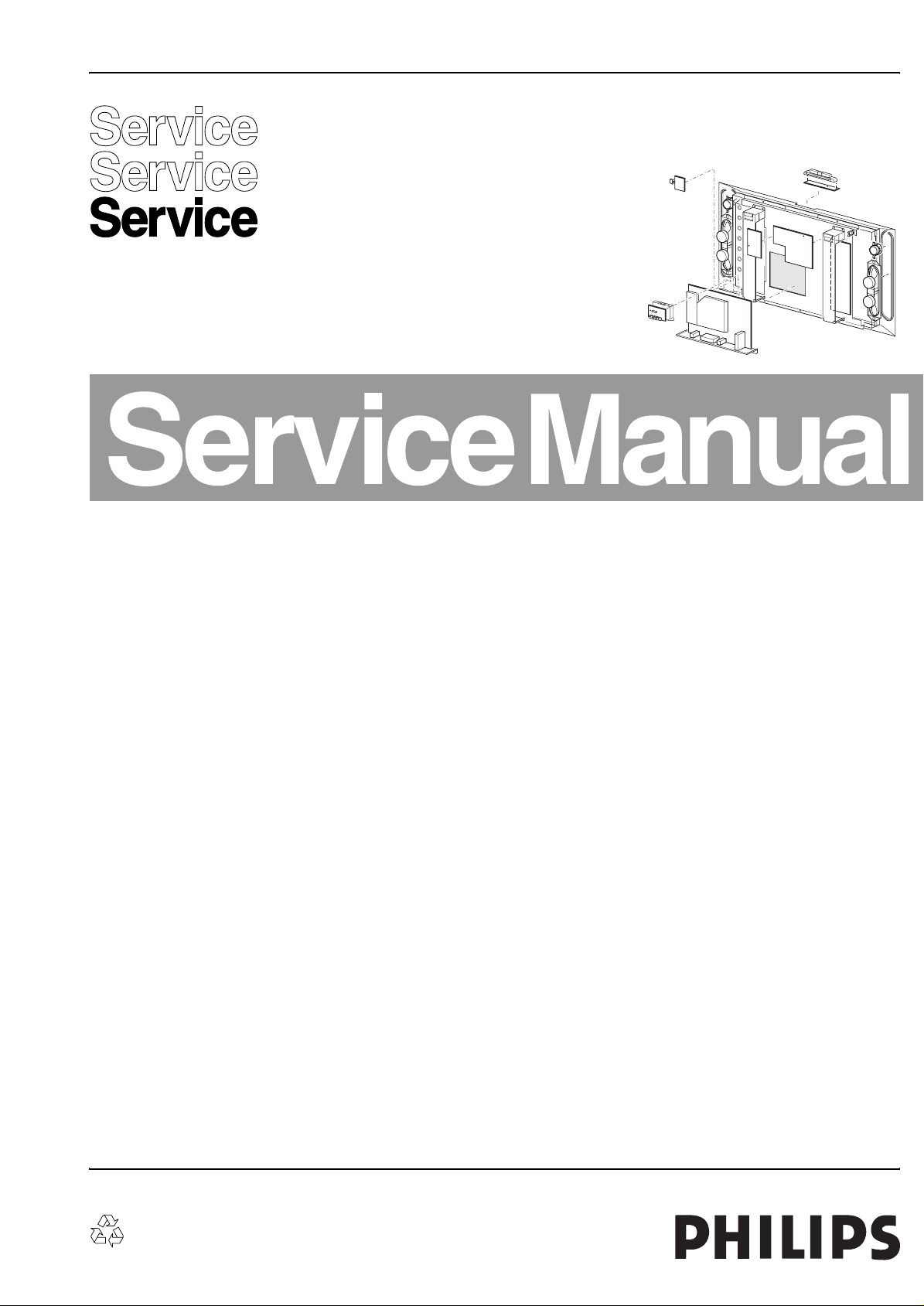
Colour Television Chassis
FTL13U
AA & AB
CL 16532149_000.eps
110703
Contents Page Contents Page
1. Technical Specifications, Connections, and Chassis
Overview 2
2. Safety Instructions, Warnings, and Notes 4
3. Directions for Use 5
4. Mechanical Instructions 17
5. Service Modes, Error Codes, and Fault Finding 20
6. Wiring Diagram, Block Diagrams, and Overviews
Wiring Diagram 31
Block Diagram Supply and Supply Lines 32
Testpoint Overview Aux and Power Supply 33
Block Diagram Video 34
Testpoint Overview Small Signal Board 35
Block Diagram Audio 36
I2C IC’s overview 37
7. Circuit Diagrams and PWB Layouts Diagram PWB
Audio Panel and Supply, DC Protection (A1) 38 45-46
Filters (A2) 39 45-46
Audio Amplifier Left High (A3) 40 45-46
Audio Amplifier Left Low (A4) 41 45-46
Audio Amplifier Right High (A5) 42 45-46
Audio Amplifier Right Low (A6) 43 45-46
Supply & DC Protection (A7) 44 45-46
Small Signal Board (AA) (B1-B20) 47-75 76-87
Small Signal Board (AB) (B1-B19) 88-102 103-114
LED/Switch Panel (LD) 115 116
LED/Switch Panel (ITV) (LD) 117 118
Side I/O (O) 119 120
Side I/O (ITV) (O) 121 122
Top Control (P) 123 124
Aux Supply (SA) 125 126-128
Power Supply (SP1) 129 131-132
Doubler (SP2) 130 131-132
8. Alignments 133
9. Circuit Descriptions, Abbreviation List, and IC Data
Sheets 137
Abbreviation list 154
IC Data Sheets 156
10. Spare Parts List 162
11. Revision List 180
©
Copyright 2004 Philips Consumer Electronics B.V. Eindhoven, The Netherlands.
All rights reserved. No part of this publication may be reproduced, stored in a
retrieval system or transmitted, in any form or by any means, electronic,
mechanical, photocopying, or otherwise without the prior permission of Philips.
Published by WO 0472 Service PaCE Printed in The Netherlands Subject to modification EN 3122 785 13481
Page 2
EN 2 FTL13U AA & AB1.
Technical Specifications, Connections, and Chassis Overview
1. Technical Specifications, Connections, and Chassis Overview
Index of this chapter:
1.1 Technical Specifications
1.2 Connections
1.3 Chassis Overview
Note: Figures below can deviate slightly from the actual
situation, due to the different set executions.
1.1 Technical Specifications
1.1.1 Vision
Display type : TFT LCD, 15:9
Screen size : 30-inch (76 cm)
Resolution (HxV) : WXGA 1280(*3)x768
Contrast ratio : 350:1
Light output : 450 cd/m
LCD response time : 16 ms
Viewing angle : 176 deg. (H)
: 176 deg. (V)
Tuning system : PLL
Color systems : NTSC 3.58
AV (playback only) : NTSC,
: PAL B/G,
: VGA (640x480),
: SVGA (800x600),
: XGA (1024x768),
: WXGA (1280x768)
Channel selections : 125 presets
: Full Cable
Aerial input : 75 ohm, F-type
Dimensions (WxHxD) in mm : 891x489x110
Hosiden: SVHS (Input)
1 - Y Ground H
2 - C Ground H
3 - Y 1 V_pp / 75 ohm j
4 - C 0.3 V_pp / 75 ohm j
Cinch (Input)
- CVBS 1 V_pp / 75 ohm jq
- Audio - L 0.5 V_rms / 10 kohm jq
- Audio - R 0.5 V_rms / 10 kohm jq
Headphone (Output) (only for consumer TV sets)
- Headphone 32 - 600 ohm / 10 mW ot
STB (only for ITV)
- RJ-11 only for ICONN jk
2
1.2.2 Rear bottom connections
Audio receiver (if present)
Audio - In (Cinch)
C - Audio - Center jq
Audio - Out (Cinch)
R - Audio - R 0.5 V_rms / 1 kohm kq
L - Audio - L 0.5 V_rms / 1 kohm kq
Audio - Out (Cinch)
R - Audio - R 0.5 V_rms / 1 kohm kq
L - Audio - L 0.5 V_rms / 1 kohm kq
1.1.2 Sound
Sound systems : AV Stereo
: BTSC (USA)
Maximum power : 2 x 10 W_rms (int.)
1.1.3 Miscellaneous
AC power voltage : 108-132 V_ac
AC power frequency : 60 Hz
Ambient temperature : +5 to +45 °C
Maximum humidity : 90 % R.H.
Power consumption :
- Normal operation : ≈ 131 W
- Standby : < 2 W
1.2 Connections
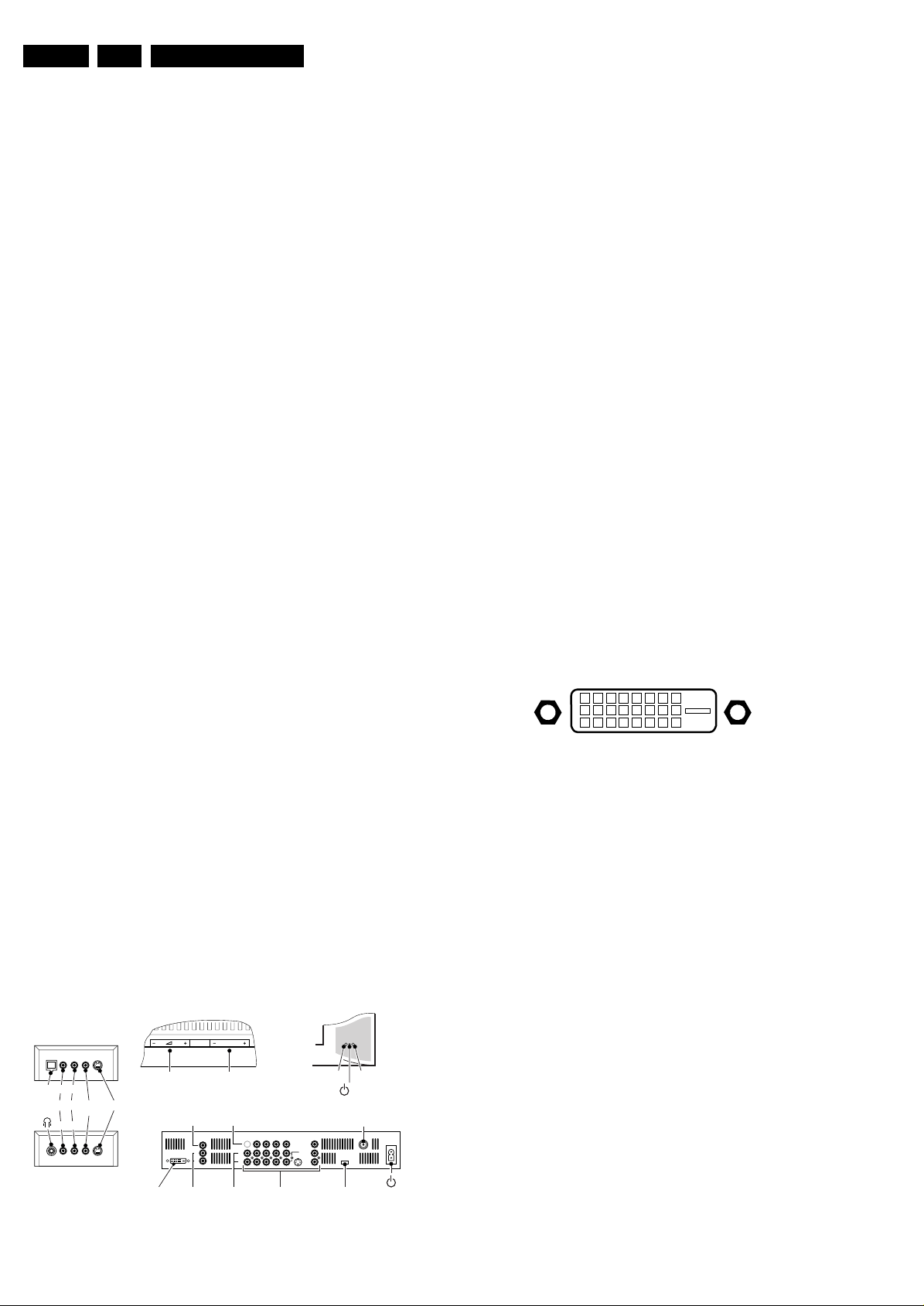
1.2.1 Side I/O (Left Bottom Side)
TOP CONTROLS
iTV only
LRSTB
Audio S-VideoCVBS-
Video
LR
Volume Program
Connections (USA Version)
PC Input (DVI)
Centre In
Audio Out
L
R
P/CHMENU/OK
No function
L
R
Audio In
MONITOR
AV4
AV1
IN
IN
VIDEO (V)LVLV
Y
L
Pb
Pr
R
RR
AV2
INOUT
VIDEO
AUDIO
S-VIDEO
IN
AUDIO
IR
AV3
IN
L
R
ServiceAV 1/2/3/4 Mains
CL 36532064_047.eps
Light sensor
Red
ANT
161003
DVI-D (Input)
18
916
17
C5
24
Figure 1-2 DVI-D Connector
1 - RX2- Data channel j
2 - RX2+ Data channel j
3 - GND Ground H
4-n.c.
5-n.c.
6 - SCL_DVI DDC clock k
7 - SDA_DVI DDC data jk
8-n.c.
9 - RX1- Data channel j
10 - RX1+ Data channel j
11 - GND Ground H
12 - n.c.
13 - n.c.
14 - +5V
15 - GND Ground H
16 - HOT PLUG
17 - RX0- Data channel j
18 - RX0+ Data channel j
19 - GND Ground H
20 - n.c.
21 - n.c.
22 - GND Ground H
23 - RXC+ Clock channel j
24 - RXC- Clock channel j
C5 - GND Ground H
Figure 1-1 Side I/O and rear connections
Page 3
Technical Specifications, Connections, and Chassis Overview
EN 3FTL13U AA & AB 1.
Monitor out
1 - CVBS 1 Vpp/75 ohm kq
2 - Audio L 0.5 Vrms/10 kohm kq
3 - Audio R 0.5 Vrms/10 kohm kq
AV1 in
1 - CVBS 1 Vpp/75 ohm jq
2 - Audio L 0.5 Vrms/10 kohm jq
3 - Audio R 0.5 Vrms/10 kohm jq
AV2 in
1 - CVBS 1 Vpp/75 ohm jq
2 - Audio L 0.5 Vrms/10 kohm jq
3 - Audio R 0.5 Vrms/10 kohm jq
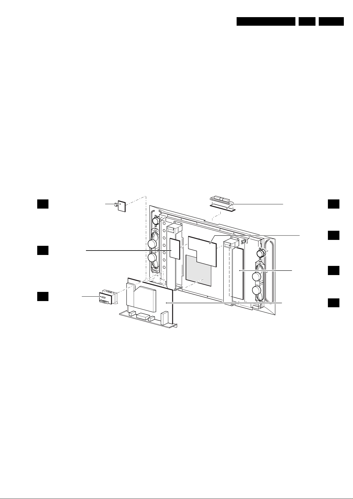
1.3 Chassis Overview
LED / MAINS SWITCH PANEL
LD
S-Video in
1 - Ground Gnd H
2 - Ground Gnd H
3 - Y 1 Vpp/75 ohm j
4 - C 0.3 Vpp/75 ohm j
AV3
1 - CVBS 1 Vpp/75 ohm jq
2 - Audio L 0.5 Vrms/10 kohm jq
3 - Audio R 0.5 Vrms/10 kohm jq
AV4 in
1-n.c.
2 - Audio L 0.5 Vrms/10 kohm jq
3 - Audio R 0.5 Vrms/10 kohm jq
4 - Y 0.7 Vpp/75 ohm jq
5 - Pb 0.7 Vpp/75 ohm jq
6 - Pr 0.7 Vpp/75 ohm jq
Aerial - In
- F-type Coax, 75 ohm D
TOP CONTROL PANEL
P
AUDIO AMPLIFIER
A
SIDE I/O PANEL
O
Figure 1-3 CBA location
AUX SUPPLY
POWER SUPPLY
SMALL SIGNAL PANEL
CL 36532053_054.eps
SA
P
SP
B
090703
Page 4

EN 4 FTL13U AA & AB2.
Safety Instructions, Warnings, and Notes
2. Safety Instructions, Warnings, and Notes
Index of this chapter:
2.1 Safety Instructions
2.2 Warnings
2.3 Notes
2.1 Safety Instructions
Safety regulations require that during a repair:
• Connect the set to the Mains (AC Power) via an isolation
transformer (> 800 VA).
• Replace safety components, indicated by the symbol h,
only by components identical to the original ones. Any
other component substitution (other than original type) may
increase risk of fire or electrical shock hazard.
Safety regulations require that after a repair, the set must be
returned in its original condition. Pay in particular attention to
the following points:
• Route the wire trees correctly and fix them with the
mounted cable clamps.
• Check the insulation of the Mains (AC Power) lead for
external damage.
• Check the strain relief of the Mains (AC Power) cord for
proper function.
• Check the electrical DC resistance between the Mains (AC
Power) plug and the secondary side (only for sets which
have a Mains (AC Power) isolated power supply):
1. Unplug the Mains (AC Power) cord and connect a wire
between the two pins of the Mains (AC Power) plug.
2. Set the Mains (AC Power) switch to the "on" position
(keep the Mains (AC Power) cord unplugged!).
3. Measure the resistance value between the pins of the
Mains (AC Power) plug and the metal shielding of the
tuner or the aerial connection on the set. The reading
should be between 4.5 Mohm and 12 Mohm.
4. Switch "off" the set, and remove the wire between the
two pins of the Mains (AC Power) plug.
• Check the cabinet for defects, to avoid touching of any
inner parts by the customer.
2.2 Warnings
• All ICs and many other semiconductors are susceptible to
electrostatic discharges (ESD w). Careless handling
during repair can reduce life drastically. Make sure that,
during repair, you are connected with the same potential as
the mass of the set by a wristband with resistance. Keep
components and tools also at this same potential. Available
ESD protection equipment:
– Complete kit ESD3 (small tablemat, wristband,
connection box, extension cable and earth cable) 4822
310 10671.
– Wristband tester 4822 344 13999.
• Be careful during measurements in the high voltage
section.
• Never replace modules or other components while the unit
is switched "on".
• When you align the set, use plastic rather than metal tools.
This will prevent any short circuits and the danger of a
circuit becoming unstable.
2.3 Notes
2.3.1 General
• Measure the voltages and waveforms with regard to the
chassis (= tuner) ground (H), or hot ground (I), depending
on the tested area of circuitry. The voltages and waveforms
shown in the diagrams are indicative. Measure them in the
Service Default Mode (see chapter 5) with a colour bar
signal and stereo sound (L: 3 kHz, R: 1 kHz unless stated
otherwise) and picture carrier at 475.25 MHz for PAL, or
61.25 MHz for NTSC (channel 3).
• Where necessary, measure the waveforms and voltages
with (D) and without (E) aerial signal. Measure the
voltages in the power supply section both in normal
operation (G) and in stand-by (F). These values are
indicated by means of the appropriate symbols.
• The semiconductors indicated in the circuit diagram and in
the parts lists, are interchangeable per position with the
semiconductors in the unit, irrespective of the type
indication on these semiconductors.
• Manufactured under license from Dolby Laboratories.
“Dolby”, “Pro Logic” and the “double-D symbol”, are
trademarks of Dolby Laboratories.
2.3.2 Schematic Notes
• All resistor values are in ohms and the value multiplier is
often used to indicate the decimal point location (e.g. 2K2
indicates 2.2 kohm).
• Resistor values with no multiplier may be indicated with
either an "E" or an "R" (e.g. 220E or 220R indicates 220
ohm).
• All capacitor values are given in micro-farads (µ= x10
nano-farads (n= x10
• Capacitor values may also use the value multiplier as the
decimal point indication (e.g. 2p2 indicates 2.2 pF).
• An "asterisk" (*) indicates component usage varies. Refer
to the diversity tables for the correct values.
• The correct component values are listed in the Spare Parts
List. Therefore, always check this list when there is any
doubt.
2.3.3 Rework on BGA (Ball Grid Array) ICs
General
Although (LF)BGA assembly yields are very high, there may
still be a requirement for component rework. By rework, we
mean the process of removing the component from the PWB
and replacing it with a new component. If an (LF)BGA is
removed from a PWB, the solder balls of the component are
deformed drastically so the removed (LF)BGA has to be
discarded.
Device Removal
As is the case with any component that, it is essential when
removing an (LF)BGA, the board, tracks, solder lands, or
surrounding components are not damaged. To remove an
(LF)BGA, the board must be uniformly heated to a temperature
close to the reflow soldering temperature. A uniform
temperature reduces the chance of warping the PWB.
To do this, we recommend that the board is heated until it is
certain that all the joints are molten. Then carefully pull the
component off the board with a vacuum nozzle. For the
appropriate temperature profiles, see the IC data sheet.
Area Preparation
When the component has been removed, the vacant IC area
must be cleaned before replacing the (LF)BGA.
Removing an IC often leaves varying amounts of solder on the
mounting lands. This excessive solder can be removed with
either a solder sucker or solder wick. The remaining flux can be
removed with a brush and cleaning agent.
After the board is properly cleaned and inspected, apply flux on
the solder lands and on the connection balls of the (LF)BGA.
Note: Do not apply solder paste, as this has shown to result in
problems during re-soldering.
-9
), or pico-farads (p= x10
-12
-6
),
).
Page 5

Directions for Use
EN 5FTL13U AA & AB 3.
Device Replacement
The last step in the repair process is to solder the new
component on the board. Ideally, the (LF)BGA should be
aligned under a microscope or magnifying glass. If this is not
possible, try to align the (LF)BGA with any board markers.
To reflow the solder, apply a temperature profile according to
the IC data sheet. So as not to damage neighbouring
components, it may be necessary to reduce some
temperatures and times.
More Information
For more information on how to handle BGA devices, visit this
URL: www.atyourservice.ce.philips.com (needs subscription,
not available for all regions). After login, select “Magazine”,
then go to “Workshop Information”. Here you will find
Information on how to deal with BGA-ICs.
2.3.4 Lead Free Solder
Philips CE is going to produce lead-free sets (PBF) from
1.1.2005 onwards.
P
b
Figure 2-1 Lead-free logo
This sign normally has a diameter of 6 mm, but if there is less
space on a board also 3 mm is possible.
Regardless of this logo (is not always present), one must treat
all sets from this date onwards according to the following rules.
Due to lead-free technology some rules have to be respected
by the workshop during a repair:
• Use only lead-free soldering tin Philips SAC305 with order
code 0622 149 00106. If lead-free solder paste is required,
please contact the manufacturer of your soldering
equipment. In general, use of solder paste within
workshops should be avoided because paste is not easy to
store and to handle.
• Use only adequate solder tools applicable for lead-free
soldering tin. The solder tool must be able
– To reach at least a solder-tip temperature of 400°C.
– To stabilise the adjusted temperature at the solder-tip.
– To exchange solder-tips for different applications.
• Adjust your solder tool so that a temperature around 360°C
- 380°C is reached and stabilised at the solder joint.
Heating time of the solder-joint should not exceed ~ 4 sec.
Avoid temperatures above 400°C, otherwise wear-out of
tips will rise drastically and flux-fluid will be destroyed. To
avoid wear-out of tips, switch “off” unused equipment or
reduce heat.
• Mix of lead-free soldering tin/parts with leaded soldering
tin/parts is possible but PHILIPS recommends strongly to
avoid mixed regimes. If not to avoid, clean carefully the
solder-joint from old tin and re-solder with new tin.
• Use only original spare-parts listed in the Service-Manuals.
Not listed standard material (commodities) has to be
purchased at external companies.
• Special information for lead-free BGA ICs: these ICs will be
delivered in so-called "dry-packaging" to protect the IC
against moisture. This packaging may only be opened
short before it is used (soldered). Otherwise the body of the
IC gets "wet" inside and during the heating time the
structure of the IC will be destroyed due to high (steam)pressure inside the body. If the packaging was opened
before usage, the IC has to be heated up for some hours
(around 90°C) for drying (think of ESD-protection!).
Do not re-use BGAs at all!
• For sets produced before 1.1.2005, containing leaded
soldering tin and components, all needed spare parts will
be available till the end of the service period. For the repair
of such sets nothing changes.
In case of doubt whether the board is lead-free or not (or with
mixed technologies), you can use the following method:
• Always use the highest temperature to solder, when using
SAC305 (see also instructions below).
• De-solder thoroughly (clean solder joints to avoid mix of
two alloys).
Caution: For BGA-ICs, you must use the correct temperatureprofile, which is coupled to the 12NC. For an overview of these
profiles, visit the website www.atyourservice.ce.philips.com
(needs subscription, but is not available for all regions)
You will find this and more technical information within the
"Magazine", chapter "Workshop information".
For additional questions please contact your local repair help
desk.
2.3.5 Practical Service Precautions
• It makes sense to avoid exposure to electrical shock.
While some sources are expected to have a possible
dangerous impact, others of quite high potential are of
limited current and are sometimes held in less regard.
• Always respect voltages. While some may not be
dangerous in themselves, they can cause unexpected
reactions that are best avoided. Before reaching into a
powered TV set, it is best to test the high voltage insulation.
It is easy to do, and is a good service precaution.
3. Directions for Use
You can download this information from the following websites:
http://www.philips.com/support
http://www.p4c.philips.com
Page 6
EN 6 FTL13U AA & AB3.
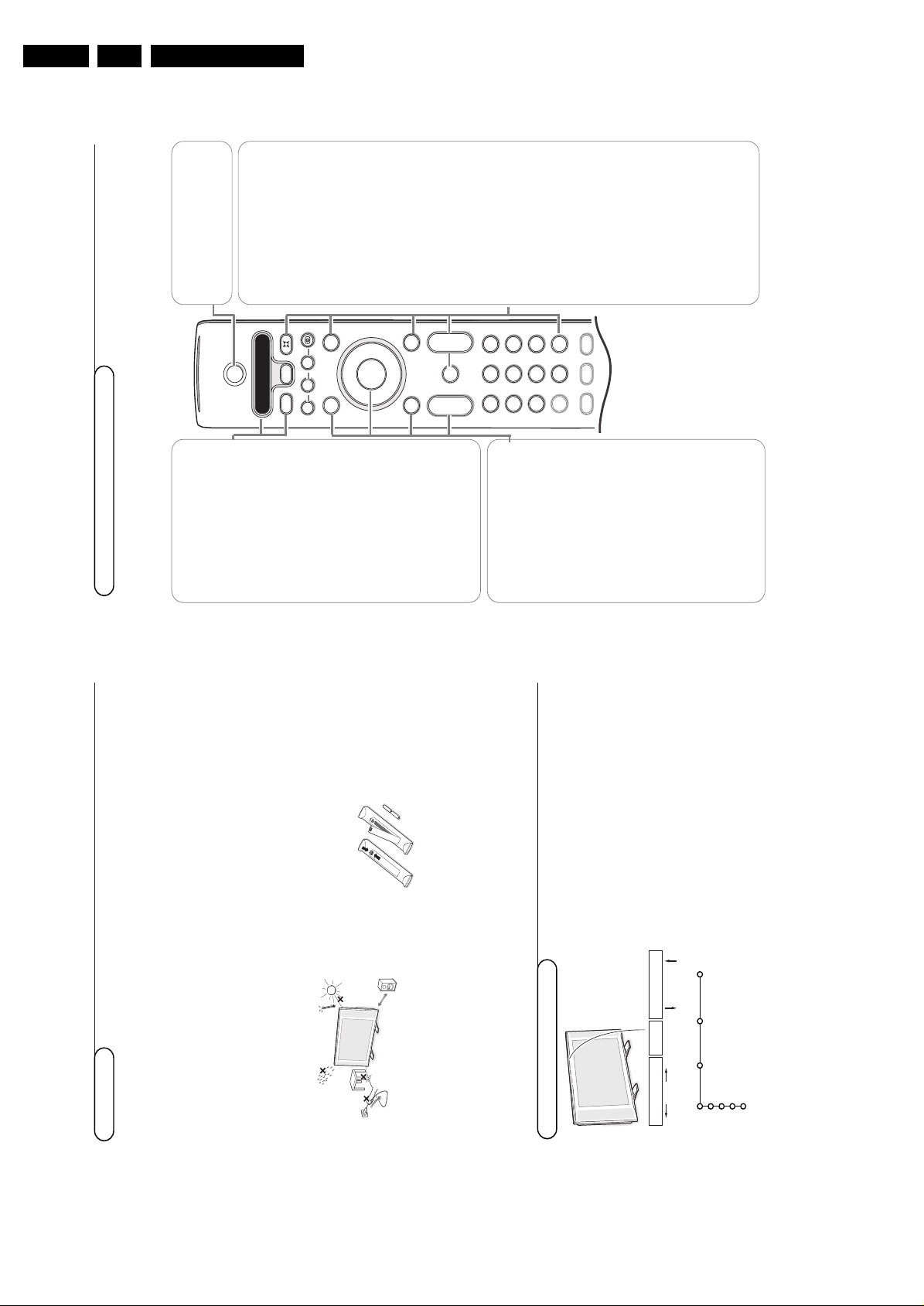
3
Use of the remote control RC4305
3
B Power
Press to turn on/off the TV.
The TV is never powered off completely
unless it is physically unplugged.
x Pixel Plus demo on/off
In the right part Pixel plus and
Digital Natural Motion is turned
on.OKPress this button to activate
your choice or to confirm when
in the menus.
S Freeze
To freeze the picture.
Dependent on the input signal,
the function may not be possible.
V Volume
Press + or - to adjust the
volume.
0/9 Digit buttons
To select a TV channel.
For a two digit program number,
enter the second digit before the
dash disappears.To switch
immediately to a selected one
digit TV channel, keep the digit
key pressed a bit longer.
® Ò ‡ π †
Audio and Video equipment buttons
See p. 19.
U
Time display
Q Sound mode
Incredible surround
With stereo transmission, and
when Incredible surround is
selected, it seems as though the
loudspeakers are spread further
apart from one another.
Virtual Dolby surround
Optimal with Dolby surround
signals. Enables you to experience
the effect of Dolby surround Pro
Logic, reproducing a rear sound
effect. See Sound menu, 3D
effect, p. 10.
Note:You can make the same
selection in the Sound menu, Sound
mode, p. 10.
l Alternate audio
When you tune a channel where
SAP (Second Audio Program) is
available, you can toggle between
Main and
SAP
. If not available,
only Main can be selected.
CC
Closed Caption
On/Off/On during mute
see p. 10
MENU
Main menu on/off
see p. 8.
¬ Mute
Interrupt the sound or restore it.
CH
Channel selection
To browse through the TV
channels or sources stored.
0 Previous TV channel
Press to display the previously
selected TV channel.
Note: For most buttons pressing a button once will activate the function. Pressing a second time will de-activate it.
When a button enables multiple options, a small list will be shown. Press repeatedly to select the next item in the
list.The list will be removed automatically after 4 seconds or press
OK
to remove immediately.
B
¬
+
-
V
+
-
CH
v
b
i
0
h
q
Select
VCR DVD SAT AMP
MENU
OK
123
456
789
0
Ò
®
‡π
†
Active Control
S
®
®
®
®
x
CBL
CC
l
l
v
Press this button repeatedly to
select
AV1
,
AV2
,
AV3
,
AV4
,
DVI
,
SIDE
or
TV
channels when in
TV mode, according to where
you connected the accessory
devices (p. 18).
CBL VCR DVD SAT AMP
Press the Select button
repeatedly to select one of the
system modes in which the
remote control can be used.
If no action is being undertaken
within 2 seconds, the remote
control returns to TV mode.
After an action in the selected
system mode the remote control
will remain in this mode for 60
seconds and will then return to
TV mode.
l Backlighting button
Press the Select button more
than 2 seconds.The backlighting
of the buttons
V
,
CH
,
¬
and
the digit buttons stays on for 5
seconds after pressing the
button.
2
Preparation
Do not insert the power plug in a wall socket
before all connections are made.
&
Wall mounting instructions
For the wall mounting instructions follow the
illustrated steps printed on the separate
template. Make sure that the wall mount is
being fixed securely enough so that it meets
safety standards.The weight of the TV (excl.
packaging) is about 38 Lbs. How to mount the
supplied stand, see the separate leaflet.
Note: other (not supplied) stands are optional
accessories. Consult your dealer.éPlace or hang the TV wherever you want, but
make sure that air can circulate freely through
the ventilation slots. Do not install the TV in a
confined space such as a book case or a
simular unit.
To prevent any unsafe situations,no naked
flame sources, such as lighted candles, should
be placed on or in the vicinity.Avoid heat,
direct sunlight and exposure to rain or water.
The equipment shall not be exposed to
dripping or splashing and no objects filled with
liquids, such as vases,shall be placed on it.
“
Insert the aerial plug firmly into the aerial
socket x at the bottom of the TV. For best
picture quality use the suppressor-aerial cable
supplied.‘To connect your computer, see p. 17.
To connect other accessory devices, see p. 14.
In order to obtain the best result, please use
only the supplied antenna cables between the
TV and videorecorder, and between
videorecorder and antenna connector.(Insert the power plug supplied into the mains
at the bottom of the TV and in the wall socket.
Refer to the rear of the TV set for the correct
operation voltage. Consult your local dealer if
your AC power supply is different.To prevent
damaging the power (AC) cord which could
cause a fire or electric shock, do not place the
TV on the cord.
§
Remote control
: Insert the 2 batteries
supplied (Type R6-1,5V).
The batteries supplied
do not contain the heavy
metals mercury and
cadmium. Please check
on how to dispose of
exhausted batteries
according to local
regulations.
è
Turn the TV on
: Press the power button B
at the right side of the TV.
A green LED and the screen light on.
The green LED blinks every time you press a
button on the remote control. When you turn on
your set for the first time, the menu language
automatically appears on the screen. Alternately the
explanation appears in different languages.
Buttons on top of the TV
Should your remote be lost or broken you can still change
some of the basic settings with the buttons on top of your
TV.
Press:
• the V - or + button to adjust the volume;
• the
-P/CH+
buttons to select the TV channels or sources.
The
MENU/OK
button can be used to summon the main
menu without the remote control.
Use:
• the V - and + buttons and the
P/CH-
and
P/CH+
buttons
to select menu items in the directions as shown;
• the
MENU/OK
button to confirm your selection.
Note:
When activated via the
MENU/OK
button on top of the TV, only
Exit
lets you dismiss the menu.
Navigate to
Exit
and press the
MENU/OK
button.
MENU/OK - V + - P/CH +
TV
Setup
Install
Demo
Exit
Picture Sound Features
Directions for Use
1m
min.
Page 7
Directions for Use
5
Installation
&
Press the
MENU
button on the remote control.
é
Use the cursor down to select
Install
.
“
Use the cursor right to select
Language
.
Follow the instructions on screen.
‘
Use the cursor up/down to select your preferred language
and press the
OK
key to confirm your selection.
(
Proceed with the
Install
menu.
The installation menu contains the following items:
Language
English
Français
Español
Install
Select the menu language
Store TV channels
Install
Language Autoprogram
Autoprogram
Install mode
Install
Install
Start
Antenna
Automatic
Cable
&
Select
Autoprogram
in the Install menu.
é
Press the cursor down to select
Install mode
.
“
Press the cursor right.
Note: It is recommended to keep the predefined
Automatic
way of
autoprogramming. In case of difficulties in autoprogramming with the
automatic method, choose for Antenna or Cable whether antenna or
cable signals are present.
When
Automatic
is selected, the TV will automatically detect
whether or not cable signal input is present.
When
Antenna
is selected, the TV will detect antenna signals
and will search for all antenna TV channels available in your local
area.
When
Cable
is selected, the TV will detect cable signals and will
search for all cable TV channels available in your local area.
‘
Press the cursor down to select
Install
.
Note: All channels must be unlocked in order to autoprogram. If
requested, enter your PINcode to unlock all channels. (See Channels
in the TV menu, p. 11.)
(
Press the cursor right.
§
The message
Searching
appears and the progress of
autoprogramming is displayed.
When Autoprogramming is complete, the puck navigates to
Stop.A message appears confirming the completion together
with the total number of channels found.
Note: when you navigate to Stop before autoprogramming is
complete, you are given the option to continue.
Available channels:
- with cable: max.from 1 to 125
- off air: max. from 2 to 69
Note: In case a particular channel is too weak for the
autoprogramming to identify, after installation is complete, you should
tune to that channel by using the digit buttons on the remote control.
If the channel is not acquired, a message will appear that the channel
is not available.
4
To use the menus
&
Press the
MENU
button on the remote control to summon
the main menu.At any moment you can exit the menu by
pressing the
MENU
button again.
é
Use the cursor in the up/down direction to select the
TV
,
Settings, Demo
or
Install
menu.
Note: Sometimes not all the menu items are visible on the screen
(indicated by a cluster of blue balls). Press the cursor down to
reveal all items.
“
Use the cursor in the left/right direction to select the menu
item.‘Use the cursor up/down again to select the control you
want to select or to adjust.
Note: Items temporary not available or not relevant are displayed
in a light grey color and cannot be selected.
B
++
v
Select
VCR DVD SAT AMP
MENU
OK
Ò
®
‡π
†
S
®
®
®
®
x
CBL
CC
l
l
cursor to select
adjustments
OK
key to
activate
return or switch
main menu on/off
i Display information
Press to display (when available) information about the selected TV
channel and program.
Menu/Remote control info
When a menu is on screen, press
i
to display info on the selected menu
item.While the menu info is displayed, press any button to display remote
control info.The normal function of the key is not executed.
b
no function
h Active control
see p. 9.
q Picture format
Press this button to summon a list of available display formats for showing
video images in the traditional 4:3 proportions.
Press this button repeatedly or press the cursor up/down to select
another picture format:Automatic, Super zoom, 4:3,Movie expand 14:9,
Movie expand 16:9, 16:9 subtitle,Wide screen or 16:9.
Automatic makes the picture fill the screen as much as possible.
Super zoom removes the black bars on the sides of 4:3 programs with
minimal distortion.
When in Movie expand 14:9, Movie expand 16:9 or Super zoom picture
format, you can make subtitles visible with the cursor up/down.
Note: in DVI mode press the q button to switch between a 4:3, 16:9 or a
Wide screen picture format.
Automatic Super zoom 4:3 Movie expand 14:9
Movie expand 16:9 16:9 subtitle 16:9 Wide screen
B
¬
+
-
V
+
-
CH
v
b
i
0
h
q
Select
VCR DVD SAT AMP
MENU
OK
123
456
789
0
Ò
®
‡π
†
Active Control
S
®
®
®
®
x
CBL
CC
l
l
EN 7FTL13U AA & AB 3.
Page 8
EN 8 FTL13U AA & AB3.
77
Time zone
This function allows you to select your local time
zone. Broadcasted time information will correct
the clock display for your local time.
&
Select
Time zone
with the cursor down.
é
Press the cursor right to select your local time
zone.
Daylight saving
Daylight saving time is automatically set by specially
broadcasted signals.This menu item allows you to
disable the automatic setting of daylight saving
time.This is useful if you live in an area or state
where daylight saving is not applied,but you receive
channels from other areas where daylight saving
signals are broadcasted.
&
Select
Daylight saving
with the cursor down.
é
Press the cursor right to select
Automatic
for
automatic clock correction for daylight saving
time, based on specially broadcasted signals.
“
Select
Off
to disable automatic clock
correction based on the specially broadcasted
signals.
Set/Change PIN
&
Select
Set
or
Change PIN
with the cursor
down.
é
If no PIN-code exists yet, the menu item is set
to
Set PIN
. Follow the instructions on screen.
If a PIN-code has previously been entered, the
menu item is set to
Change PIN
. Follow the
instructions on screen.
All number combinations from 0000 to 9999
are valid numbers.
“
The General menu reappears with a message
confirming that the PIN has been created.
Important:You have forgotten your PIN !
&
Select
Change PIN
in the General menu and
press
OK
.
é
Press the cursor right to enter the overriding
PIN-code 0-7-1-1.
“
Press the cursor again and enter a new
personal 4-digit PIN code.The previous code is
erased and the new PIN-code is stored.
&
Select
Source
with the cursor right.
é
Press the cursor down to select one of the external AV inputs.“Press the cursor right to enter the list of types of devices
attached to the selected input.
‘
Select the accessory device with the cursor up/down.
Once you have named the source, e.g.VCR, this source will
automatically be selected when your remote control is in VCR
mode, see p. 3, and when you press the v button on the
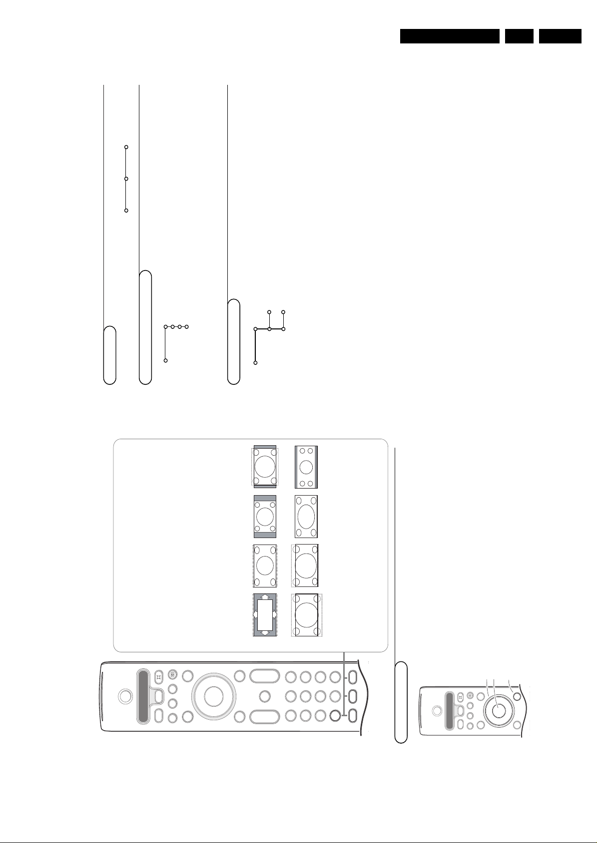
remote control.(Press the
MENU
button on the remote control to turn off all
menus on screen.
§
Press the v button on the remote control.
The Source Select menu appears in which you may select a
source or peripheral connected to be displayed on screen.
Center input - Center in volume
When you have connected a multichannel surround receiver to
the TV, the loudspeakers of the monitor can act as center
speaker, making a separate center speaker unnecessary;
Select
Center input On.
When having selected
On
you can adjust the Center in volume
with the cursor left/right to correct volume level differences of
the external audio receiver and speakers.
Source
AV1
AV2
AV3
YPbPr
FRONT
Center input
Center in volume
Settings
Source
6
General
Menu background
&
Select
Menu Background
with the cursor
down and press the cursor right.
é
Select
On
or
Off
to turn the menu background
on or off.
Reset AV settings
This function allows you to reset most of the
picture and sound settings to their predefined
factory states.
& Select
Reset AV settings
with the cursor
down.
é
Press
OK
to erase settings and reset them to
their default values.
Caption Service
Closed Captioning allows you to read the voice
content of television programs on the TV
screen. Designed to help the hearing impaired,
this feature uses on-screen ‘text boxes’ to
show dialogue and conversations while the TV
program is in progress. Captions will appear on
the screen during captioned broadcasts.
Note:The captions do not always use correct
spelling and grammar. Not all TV programs and
product commercials are made for broadcast with
Closed Caption information included. Refer to your
area’s TV program listings for the TV channels and
times of Closed Caption shows. The captioned
programs are usually noted in the TV listings with
service marks such as ‘CC’.
&
Select
Caption service
with the cursor down.
é
Press the cursor right.
“
Select the desired
Caption Service:
• CC 1, 2,3 or 4
Dialogue (and descriptions) for the action on
the captioned TV program shows on screen.
Usually CC 1 is the most used.CC 2 may be
used for alternate languages if they are being
transmitted.
• T 1, 2,3 or 4
Often used for channel guide, schedules,
bulletin board information for Closed Caption
programs, news, weather informations or
stock market reports.
Not all Caption Services are necessarily being
used by a TV channel during the transmission of a
Closed Caption program.
‘
See Closed Captions in the TV, Features menu,
see p. 10, to turn the
Caption service On
or
Off
.
Note:This television provides display of television
closed captioning conforming with the EIA-608
standard and in accordance with Sections 15.119
of the FCC rules.
OSD (On Screen Display)
&
Select
OSD
with the cursor down.
é
Press the cursor right to select Normal or
Minimum.
Normal to activate the continuous display of
the channel number and extended display of TV
channel and channel information on screen.
Minimum to activate the display of reduced
channel information.
See Use of the Remote Control, p. 4, Display
information.
Note: When Closed Captions is switched on, see
Features, p. 14, continuous display of the channel
number is not possible
This menu allows you to change various settings that are presumably adjusted less frequently than most
other settings.
Settings menu
General Source
TV
Settings
Demo
Install
The
General
menu allows you to change settings that will
typically be accessed only occasionally.
The
Source
menu allows you to select a source.
General
Menu background
Reset AV settings
Caption Service
OSD
Time zone
Daylight saving
Set/Change pin
Settings
Directions for Use
Page 9
Directions for Use
9
Dynamic contrast
Automatically makes the contrast in the darker and
the brighter picture areas more noticeable as the
image on the screen changes.
Normally, select
Medium
. It may be preferred to
select
Minimum
,
Maximum
or
Off
.
&
Press the cursor right to enter the list.
é
Select one of the settings with the cursor
up/down.“Press the cursor left to return to the picture
menu.
DNR (Digital Noise Reduction)
Automatically filters out and reduces the image
noise and improves picture quality when receiving
weak video signals.
&
Press the cursor right to enter the list.
é
Select
Off
,
Minimum
,
Medium
or
Maximum
according to the image noise.“Press the cursor left to return to the picture
menu.
Color enhancement
When activated, this feature automatically controls
green enhancement and blue stretch. It makes the
colors more vivid.
&
Press the cursor right.
é
Select
On
or
Off
in order to activate/de-
activate Color enhancement with the cursor
right.
Tint
Allows you to select the color mix (hue) of the
picture.
Picture format
This menu item performs the same as the q
button on the Remote Control. See Use of the
Remote Control, p. 4.
The TV continuously measures and corrects all
incoming signals in order to provide the best
picture possible.
&
Press the h button on the remote control.éThe Active Control menu appears.“Press the cursor up/down to select the Active
Control values
Off
,
Minimum
,
Medium
(recommended) or
Maximum
.
The picture settings are being optimized
continuously and automatically which is
displayed by bars.The menu items can not be
selected.
‘
Press the cursor right to select
Auto Picture
.
(
Press the cursor up/down to select one of the
predefined picture settings.§Press the cursor right to select
Active
Display
.
è
Press the cursor up/down to select
Show bars
,
one of the Dual screen demos or
Off
.
When you select Dynamic contrast, Pixel Plus,
Digital Noise Reduction or Digital Natural
Motion, the TV screen is divided into two parts:
in the left part the selected picture quality
setting is switched off; in the right part it is
switched on.
Note: Dependent on the input signal, one or more
Dual screen demos may not be selectable.
!
Press the h button again to switch off the
Active Control menu.
Note: Active Control is not available for digital signals via
AV4 or DVI.
Active Control
&
Select
Demo
in the Main menu with the
cursor down.
é
Select
Auto demo
or one of the features with
the cursor right and press the
OK
button on
the remote control.
If
Auto demo
has been selected the demo will
automatically present all the features sequentially in
a loop. Press one of the cursor buttons to stop the
Auto demo.
If one of the features has been selected, this
particular feature demo will run one time only,until
activated again, and the Demo menu will reappear.
Digital options, Light sensor and 3D Y/C
Comb filter On or Off
Select
Digital options, Light sensor
and
3D Y/C
Comb filter On
or
Off
to really see the difference
in picture quality.
In Dealer Demo mode it is possible to change
channels with
- CH +
and to adjust the volume.
Note: the Dealer Demo is not part of the automatic
sequence and can only be activated separately.
8
&
Press the cursor right to select
Picture
.
é
Select the menu items in the Picture menu with the cursor
up/down.“Adjust the settings with the cursor left/right or enter the
list of submenu items with the cursor right. Select a
submenu item with the cursor up/down.
Note:To remove the menu background before adjusting the
picture settings, see Select TV setup, General, p. 6.
Auto picture
Select
Auto picture
to display a list of predefined picture
settings, each corresponding with specific factory settings.
Personal
refers to the personal preference settings of
picture in the picture menu.
Digital processing
•
Progressive scan
= line doubling eliminates line flicker.
•
Pixel Plus
= is the most ideal setting, but you may
consider to select Movie Plus in case a halo effect should
disturb you. Dependent on your own preference, select
Progressive scan (without motion compensation).
Note: Interference, caused by fluorescent lights just above the
TV, may occur when having selected Pixel Plus.
TV menu
Press the
MENU
button on the remote control to summon the main menu.
Note: Dependent on the input signal, one or more menu items may not be selectable.
Press the i button on the remote control to get information about the selected menu
item.
Picture Sound Features Channels
Auto picture
Contrast
Brightness
Color
Sharpness
Color temperature
Digital processing
Dynamic contrast
DNR
Color enhancement
Tint
Picture format
TV
Picture menu
Demo
Auto demo
...........
Dealer demo - Digital options
- Light sensor
- 3D Y/C Comb filter
TV
Settings
Demo
Install
Note:
Sharpness, Digital processing, Dynamic
Contrast, DNR, Color enhancement, Tint
and Picture format are not available for
HD sources.
EN 9FTL13U AA & AB 3.
Page 10
EN 10 FTL13U AA & AB3.
1111
On timer
Note:The On timer function is only available if time
information is available via the local PBS channel.
&
Select
On timer
with the cursor down.
é
Press the cursor right and select
On
or
Off
to
set the On timer On or Off.
“
When you have selected
On
press the cursor
right.
‘
Select the TV channel or external source you
want the On timer to activate with the cursor
up/down.(Press the cursor right to select the day you
would like the On timer to become active.
Select
Daily
to set the On timer for daily
operation on the selected TV channel or
source.
§
Press the cursor right to select
AM
or
PM
.
è
Press the cursor right to enter the time with
the digit buttons or with the cursor up/down,
left/right.!Press the
OK
button to confirm.
ç Press the
MENU
button to turn off all menus
on screen.
Zoom
Note: Dependent on the input signal, Zoom may not be
selectable.
&
Select
Zoom
with the cursor down and press
the
OK
key.
é
Press the
OK
key to select one of the zoom
magnifications (x1, x4,x9, x16).
“
Additionally you can shift the selected zoom
window over the screen with the cursor keys
up/down, left/right.‘Press the
MENU
key to turn off the zoom
function.
Channels menu
Picture Sound Features Channels
Channel list
Lock after
Channel lock
TV ratings lock
Movie ratings lock
Channel remove
TV
Settings
Demo
Install
...
TV-Y
TV-Y7 (D) Dialogue
TV-PG (L) Language
TV-14 (S) Sex
TV-MA (V) Violence
&
Press the cursor right to select
Channels
.
é
Select the menu items with the cursor
up/down and adjust the settings with the
cursor left/right.
Use the on-screen Menu-Info
i
for more
information about the menu items.
TV Ratings Lock
Your TV is equipped with a V-chip.This allows you
to control access to individual programs based on
their movie and TV ratings.All settings apply to all
AV inputs, except AV3 and AV4.
The program content advisory data are sent by the
broadcaster or program provider.
&
Select
TV ratings lock
with the cursor down.
A list appears, showing the age-based TV ratings
and a corresponding content-based ratings list.
é
Press the cursor right to enter the list.
“
Select an age-based TV rating with the cursor
up/down, and enter, if present, the list with
content-based ratings with the cursor right, and
select one content-based rating.
‘
Press
OK
to activate/de-activate the selected
rating.You are asked to enter your PIN. (See
Set/Change PIN, p. 12).If the code is correct,
the TV ratings lock menu reappears.
(
Select another content-based rating if you like
and press
OK
again.
You need only enter your PIN-code once while
the menu is active.You can lock/unlock any
number of ratings on the list without re-
entering your code.
1010
&
Press the cursor right to select
Sound
.
é
Select the menu items in the Sound menu with the
cursor up/down and adjust the settings with the cursor
left/right. Remember, control settings are at normal mid-
range levels when the bar scale is centered.
Auto sound
Select Auto sound to display a list of predefined sound
settings, each corresponding with specific factory
settings of Treble and Bass.
Press the cursor right to enter the list.
Press the cursor up/down to select a predefined sound
setting.
Personal
refers to the personal preference settings of
sound in the Sound menu.
Note: the moment you are in a predefined Auto sound setting
and you modify a setting in the Sound menu, all values of the
menu will overwrite the previously made personal setting.
Sound
Auto sound
Equalizer
Volume
Balance
Headphone volume
Sound mode
Alt audio
(Mono/Stereo)
3D surround effect
AVL
Delta volume
TV
Sound
OffOnOn during mute
Features
Closed Captions
Sleep Timer
On timer
Zoom
TV
Features menu
&
Press the cursor right to select
Features
.
é
Select the menu items with the cursor up/down and
adjust the settings with the cursor left/right.
Use the on-screen Menu-Info
i
for more information
about the menu items.
Closed Captions
See also Caption Service, Settings menu, General,
p. 6.
&
Select
Closed Captions
with the cursor down.
é
Press the cursor right.
“
Select
On
,
Off
or
On during mute
When
On
is selected, the TV will display the
currently display Caption Service, assuming that
the service is available in the broadcast.
When
Off
is selected, the TV will not display
Closed Captions information;
When
On during Mute
is selected, the TV will
display the currently selected Caption Service
when the mute function is active.
When the mute function is not active, the TV
will not display Closed Captions informations.
Sleep Timer
With the Sleep timer function you can set a time
period after which the TV will turn itself off.
&
Select
Sleep Timer
with the cursor down.
é
Press the cursor right to set the time
The cursor runs from 0 up to 180 mins
(in 5-min increments).When set to 0, the sleep
timer is turned off.
One minute before the sleep timer expires, a
message appears that the TV will turn off in
60 seconds or you may cancel the sleep timer
by pressing the
OK
button.You can always turn
off your TV earlier or change the set time.
Directions for Use
Page 11
Directions for Use
13
Movie Ratings Lock
This function allows you to control access to
individual movies based on their MPAA ratings
(Motion Picture Association of America).
&
Select
Movie ratings
lock with the cursor
down.A list appears, showing all valid MPAA
content ratings.
é
Press the cursor right to enter the list.
“
Select a movie rating with the cursor up/down.‘Press
OK
to activate/de-activate the selected
rating.
You are asked to enter your code. (See
Set/Change PIN, p. 12.) If the code is correct,
the Movie ratings lock menu reappears.
Each rating item has a box-graphic in front of it to
indicate whether or not programs carrying that
rating are currently locked:
• a yellow-colored box: movies with this rating are
locked;
• a blue-colored box: movies with this rating are
unlocked.
When
All
has been selected, all items on the
movie ratings list become selected. (All movies are
locked.)
If, while
All
is selected, any other item is
unselected, then
All
is automatically unselected.
When
NR
has been selected, no other item is
selected.
When any other item has been selected, all ratings
below are selected as well, thus all movies with
those ratings will be locked.
NR
not ratedGmovies with a mild content, suitable for all
agesPGmovies for which parental guidance is
recommended.
They may contain a few racy or violent
scenes or maybe some bad language
PG-13
movies for which parental guidance may be
recommended if under age 13
R
restricted.The movies usually contain
offensive sex or bad language and may be
unsuitable for children under the age of 17.
Parental guidance or permission needed.
NC-17
even with parental permission, forbidden
under age 17.
More offensive sex, violence or bad
language.Xmovies which generally focus on sex,
violence and/or bad language. Also known
as pornography.
Picture Sound Features Channels
Channel list
Lock after
Channel lock
TV ratings lock
Movie ratings lock
Channel remove
TV
Settings
Demo
Install
Channel remove
This feature provides the ability to remove a
channel number from the channel list.
&
Select
Channel remove
with the cursor down.
é
Press the cursor right to enter a list with all
stored channel numbers.“Select the channel you want to remove with
the cursor down.‘Press
OK
.
(
Repeat to remove other channels.
Picture Sound Features Channels
Channel list
Lock after
Channel lock
TV ratings lock
Movie ratings lock
Channel remove
TV
Settings
Demo
Install
12
Each ratings item has a box-graphic in front of it to
indicate whether or not programs carrying that
rating are currently locked:
• a yellow-colored box: all items in the contents-
based list are locked as well;
• a blue-colored box: the item is unselected;
• a half blue, half yellow-colored box: some
content-based ratings are selected/unselected.
When
All
has been selected, all items in the age-
based and in the contents-based lists are locked.
If, while
All
is selected, any other item, either an
age-based or content-based item, is unselected,
then All is automatically unselected.
None
is the selection for items that either have no
rating information or have a rating of None. Both
will be locked.
When an item on the age-based list is selected, all
items below that item of the same group are
locked as well.
When you select a content-based rating, all
identical content-based ratings in the younger age-
based categories are also selected.
Age-based Rating Content-based Rating
All none
None none
TV-Y none
TV-Y7 (FV) Fantasy Violence
TV-G none
TV-PG (D) Dialog
(L) Language
(S) Sex
(V) Violence
TV-14 (D) Dialog
(L) Language
(S) Sex
(V) Violence
TV-MA (L) Language
(S) Sex
(V) Violence
TV-Y
appropriate for children of all ages with themes
and elements suitable for children aged 2-6
TV-Y7
programs designed for children age 7 and older
TV-Y7-FV
programs include fantasy violence more intense
than other programs in the TV-Y7 category
TV-G
programs suitable for all ages.These programs
contain little or no violence, no strong language
and little or no sexual dialogue or situations
TV-PG
programs contain elements that some parents may
find unsuitable for younger children and which may
need parental guidance.
The program may contain moderate violence,
sexual dialogue and/or situations and some strong
language.
TV-14
programs contain elements that may not be
suitable for children under 14 years of age.These
programs include one or more of the following:
intense violence, intense sexual
situations,suggestive dialogue and strong language.
TV-MA
programs are designed to be viewed by adults and
may be unsuitable for children under the age of 17.
These programs may contain graphic violence,
explicit sexual activity and/or crude or indecent
language.
EN 11FTL13U AA & AB 3.
Page 12
EN 12 FTL13U AA & AB3.
151515
&
Connect the satellite antenna cable or
the Cable TV cable 1 to the satellite
receiver’s or cable box’s
IN
jack.
é
To hear stereo sound on your TV
connect the Video,Audio left and right
AV cables 2 to the
VIDEO
,
L AUDIO
and
R AUDIO
input jacks of
AV1 IN
or
AV3 IN
.
If your satellite receiver or cable box
has an S-Video jack:
For improved picture quality, connect an
S-Video cable to the
S-VIDEO
input
instead of connecting the satellite
receiver or cable box to the
VIDEO
jack
of
AV2 IN
.
Connect the audio cables to the device’s
AUDIO L
and
R
jacks and to the
L
AUDIO
and
R AUDIO AV2
jacks on the
TV.
SAT / Cable Box
IN
CABLE
AV 4
R
L
AUDIO AUDIO
AUDIO
NO
FUNCTION
Pr
Pb
Y
IN
AV 1
IN
AV 3
IN
IN
S-VIDEO
VIDEO (V)
L
V
R
L
V
R
L
R
L
VIDEO
AV 2
INOUT
MONITOR
RR
OUT
VIDEO
L/Mono
R
2
CABLE
RECORDER
Cable Box
3
2
OUT
OUTINOUTIN
75
SIGNAL
SPLITTER
ANTENNA
4
Recorder and Cable Box with RDF output
&
Use an optional signal splitter.éConnect one of the cable TV signal
splitter outputs 1 to the cable box’s INjack.“Connect the other cable TV signal
splitter output 2 to the 75 ø x plug
on the bottom of the TV.
‘
Connect the cable box’s
OUT
jack 3
to the recorders
RF IN
socket.
(
Connect the Video, Audio Left and Right
(only for stereo sound) AV cables 4 to
the
VIDEO
,
AUDIO L
and
R
input
AV2
IN
jacks on the TV.
Satellite Receiver / Cable Box with AV outputs
&
Connect your satellite receiver or cable
box as described above.éConnect your recorder as described on
the previous page.“Connect the AV cables 1 to the
satellite receiver’s or cable box’s
AV
OUT
jacks and to the recorder’s
AV I N
jacks.‘Connect the recorder’s
AV OUT
jacks
2 to the TV’s
AV2 IN
jacks.
RECORDER
OUT
OUT
IN
VIDEO
L/Mono
R
AV 4
R
L
AUDIO
AUDIO
NO
FUNCTION
Pr
Pb
Y
IN
AV 1
IN
IN
S-VIDEO
VIDEO (V)
L
V
R
L
V
R
L
AV 2
IN
OUT
MONITOR
RR
2
1
OUT
SAT / Cable Box
AUDIO
AV 3
IN
R
L
VIDEO
Recorder and Satellite Receiver / Cable Box with AV outputs
141414
There is a wide range of audio and video devices that can be connected to your TV.The following
connection diagrams show you how to connect them to the TV.
AV1 IN
can handle CVBS;
AV2 IN
CVBS and Y/C;
AV3 IN
CVBS; and
AV4 IN
YPbPr 480p, YPbPr 1080i;
FRONT
: CVBS and Y/C.
Recorder (
VCR
-
DVD
+
RW
)
Note: Do not place your recorder too close to the screen as some recorders may be susceptible for signals out of the
display. Keep a minimum distance of 20” to the screen.
CABLE
RECORDER
75
ANTENNA
OUT
OUTIN
VIDEO
L/Mono
R
AV 4
R
L
AUDIO
AUDIO
NO
FUNCTION
Pr
Pb
Y
IN
AV 1
IN
IN
S-VIDEO
VIDEO (V)
L
V
R
L
V
R
L
AV 2
INOUT
MONITOR
RR
3
IN
RECORDER
VIDEO
L/Mono
R
AV 4
R
L
AUDIO
AUDIO
NO
FUNCTION
Pr
Pb
Y
IN
AV 1
IN
IN
S-VIDEO
VIDEO (V)
L
V
R
L
V
R
L
AV 2
INOUT
MONITOR
RR
VIDEO
L/Mono
R
54
x
TV
Connect Accessory Devices
&
Connect the RF Antenna or Cable TV
cable (eventually via an optional two-way
signal splitter and/or Cable TV converter
box) 1 to the
RF IN
socket of your
recorder.
é
Connect another RF cable 2 from the
output
OUT
of your recorder to the
TV’s input 75 ø x jack.
“
Better playback quality can be obtained if
you also connect the Video,Audio Left
and Right (only for stereo devices) AV
cables 3 to the
VIDEO
,
AUDIO L
and
R
input jacks of
AV2 IN
.
If your recorder has an S-VHS video
jack:
For improved picture quality, connect an
S-video cable with the
S-VIDEO
input
instead of connecting the recorder to
the
VIDEO
jack of
AV2 IN
.
S-Video does not provide audio, so audio
cables must still be connected to provide
sound.
Recorder and other A/V devices
Recorder&Connect your recorder as described
above 3.
The
MONITOR OUT
connectors can be
used for daisy chaining or to record
programs from your TV 4.
See Record with your recorder, p. 19.
Other A/V devices
é
Connect the Video,Audio left and Audio
right (only for stereo devices) cables to
the
VIDEO
,
AUDIO L
and
R
input jacks
of
AV1 IN
5 or the front connections
(see p. 18).
Note: in case of mono equipment, only the
left loudspeaker reproduces sound. Use a
mono to stereo adapter (not supplied) for
sound reproduction via all internal
loudspeakers.
Directions for Use
Page 13
Directions for Use
17171717
DVI connector (AV5)
S•VIDEO
VIDEO
L
R
AUDIO
DVI
1
2
The
DVI IN
connector allows
- the following TV and monitor display modes:
EDTV 640/720 x 480p
720 x 576p
HDTV 1920 x1080i
VGA 640 x 480 60 Hz
SVGA 800 x 600 56 Hz
XGA 1024 x 768 60 Hz
- uncompressed HD content
- encrypted or non encrypted signals.
Note: Only Single Digital Link DVI is supported.
&
Connect the digital DVI output of your HD device (e.g.
PC, DVD player, Set Top Box..) to the
DVI IN
connector
of your TV.
é
Connect the audio cable 2 of your HD device (if
audio is present) to the
AUDIO
outputs of your HD
device and to the
AUDIO R
(right) and
L
(left) inputs of
the panel of the TV.
Notes:
- Proper working is only guaranteed with DVI compliant consumer
products.
- Digital devices from different manufacturers have the possibility
of differing output standards which may cause difficulties for the
television to properly display;
- If the set is cold, there may be a small “flicker” when the set is
turned on. this is normal, there is nothing wrong with the set.
- If possible, use the VESA 1024x768@60Hz video mode to
obtain the best image quality for your LCD monitor.
DVI is a specific digital input allowing
encrypted transmission of
uncompressed HD content. DVI
includes HDCP (high-bandwidth
digital content protection), which is
supported by Hollywood, satellite
providers, and most of the consumer
electronics industry. DVI is gaining
monumentum and quickly becoming
an industry standard for the
consumers to view high-definition
material while keeping content
protected.
&
Connect the audio cable to the multi channel Surround receiver
and to
AUDIO OUT L
and
R
below the
CENTRE IN
connector
of your TV 1.
Note: turn off the TV and your sur round receiver before connecting
them. Set the Surround receiver’s volume to minimum.
é
If you want the loudspeakers of your monitor to act as center
speaker, also connect an audiocable to the multi channel
Surround receiver and to the
CENTRE IN
of your TV 2.
“
Select
Center Input On
in the Source menu. See p. 7.
The loudspeakers of the TV will now only produce center
sound, the loudspeakers connected to the audio receiver will
produce Surround Sound.The volume has to be controlled via
the multi channel Surround receiver.
Note: No sound will be heard when a TV channel or external source is
blocked via the Channel Lock menu (see p. 11).
Multi channel Surround receiver
S•VIDEO
VIDEO AUDIO
LR
L
R
CENTRE
IN
1
2
CENTRE IN
OUT
AUDIO
16
DVD Player or other accessory digital source devices
Devices with AV connectors only
&
Connect the video cables to the device’s
AV OUT
jacks
and to the TV’s
AV1
,
AV2
or
AV3 IN
jacks.
é
Connect the audio cables to the device’s
AUDIO L
and
R
jacks and to the
L AUDIO
and
R AUDIO AV1
,
AV2
or
AV3
jacks on the TV. (According to where you
connected the video cables, to
AV1
,
AV2
or
AV3
.)
Devices with an S-Video connector
&
Connect an S-Video cable to the
AV2 S-VIDEO
input.
Note: When using the
S-VIDEO
connector do not connect
any device to the
AV2 VIDEO
input.
é
Connect the audio cables to the device’s
AUDIO L
and
R
jacks and to the
L AUDIO
and
R AUDIO AV2
jacks on
the TV.
Devices with Component Video Output Connectors
(DVD, Set Top Box,...)
&
Connect the cables of your
YPbPr
equipment 1 to
the
YPbPr
input
AV4 IN
sockets on the TV.
é
Connect the Audio left and right (only for stereo
devices) cables 2 to the
AUDIO L
and
R
input of
AV4
.
VIDEO
L/Mono
R
AUDIO
S-VIDEO
1 2
DVD
AV 4
R
L
AUDIO AUDIO
AUDIO
NO
FUNCTION
Pr
Pb
Y
IN
AV 1
IN
AV 3
IN
IN
S-VIDEO
VIDEO (V)
L
V
R
L
V
R
L
R
L
VIDEO
AV 2
INOUT
MONITOR
RR
Devices with Progressive scan output (e.a. a digital Set Top box, a video game console or a
Progressive scan DVD player (480p or 1080i)
Connect the device with 2Fh YPbPr output to the
YPbPr
jacks and to the
L
and
R AUDIO
jacks of
AV4
.
Note:s
- The labels for the component video sockets may differ depending on the DVD player. Although the
abbreviations may vary, the letters B and R stand for the blue and red component signals, respectively, and Y
indicates the luminance signal. Refer to the DVD player’s instructions for use for definitions and connection
details.
- This television is designed to accept high definition signal standards 1080i and 480p as specified by the
Electronic Industries Association standard EIA770.3.
Digital devices from different manufacturers have the possibility of differing output standards which may
cause difficulties for the television to properly display.
Warning
: in case you notice scrolling images, wrong colors or no colour, no picture, or even combinations of
these on your screen, check if the connections are done in the correct way or move your digital device further
away from your TV.
EN 13FTL13U AA & AB 3.
Page 14
EN 14 FTL13U AA & AB3.
19191919
Audio- and video equipment keys
Most of the audio and video equipment from our range of products can be
operated with the remote control of your TV.
Press one of the buttons after you pressed the
Select
button repeatedly
according to the equipment you want to operate with this remote control.
See Use of the remote control, p. 5.
B
¬
+
-
V
+
-
CH
v
b
i
0
h
q
Select
VCR DVD SAT AMP
MENU
OK
123
456
789
0
Ò
®
‡π
†
Active Control
S
®
®
®
®
x
CBL
CC
l
l
B to switch to standby (
VCR
)
S for pause (
DVD
,
CD)
® for record,
Ò for rewind (
VCR
,
CD
);
search down (
DVD
,
AMP
)
‡ for stop,
π for play,
† for fast forward (
VCR
,
CD
);
search up (
DVD/AMP
)
i display information
MENU
to switch the menu on or
off
- CH +
for chapter, channel, track
selection
0 to 9 digit entry,
0 tape index (
VCR
),
select a DVD chapter,
select a frequency (
AMP
)
U VCR timer
Q surround on/off (
AMP
,
CD)
cursor up/down
to select the next or the
previous disc (
CD)
cursor left/right
to select the previous or
following track (
CD
)
Record with your recorder
Notes:
- If no action is being undertaken within 60 seconds, the remote control returns to
TV mode.
- After an action in the selected system mode, the remote control will remain in
this mode for 60 seconds and will then return to TV mode or press the
Select
button to return to TV mode immediately.
To record S-VHS quality, connect an S-VHS
peripheral directly to the recorder.
Record a TV program
You can record a TV program using your recorders
tuner without affecting your TV.
&
Select the channel number on your recorder.éSet your recorder to record.
See the handbook for your recorder.
Switching channel numbers on your TV does not
disturb recording !
Record a recorder from
MONITOR OUT
You can record a program on your recorder from
the TV tuner via
MONITOR OUT
.
&
Switch on the device.éSelect the correct channel on your TV and the
correct input on your recorder.“Set your recorder to record.
You record the tuner channel of the TV, even
when you switch to an AV input using the v
button on the remote control.
Do not switch channels or turn off your TV when
you are recording through
MONITOR OUT
.
Note: When a TV channel or AV source is blocked
because of a rating set via the Channels menu (see
p. 12), also the record output picture and sound are
muted.
18
Front connections
Camera or Camcorder
&
Connect your camera or camcorder as shown.éConnect to
VIDEO
2 and
AUDIO L
3 for mono
equipment. For stereo equipment also connect
AUDIO R
3.
S-VHS quality with an S-VHS camcorder is obtained by
connecting the S-VHS cables with the S-video input 1 and
audio inputs 3.
Do not connect cable 2 and 3 at the same time.This may cause
picture distortion !
Headphone
&
Insert the plug into the headphone socket L as shown.éPress ¬ on the remote control to switch off the internal
loudspeakers of the TV.
The headphone impedance must be between 8 and 4000 Ohm.The
headphone socket has a 3.5 mm stereo jack.
In the Sound menu select
Headphone volume
to adjust the
headphone volume.
ANTENNA
SERVICE
75
S•VIDEO
VIDEOAUDIO
LR
S
•
VHSVH
S
AUDIO
A
U
D
I
O
VIDEO INVI
D
EO IN
S
•VHS
AUDIO
VIDEO IN
L
R
1 2
3
L
&
Press the v button repeatedly or select
Source
in the
Settings menu (see p. 7) to select
AV1
,
AV2
,
AV3
,
AV4
,
FRONT
,
DVI
or
TV channels
, according to where you connected your
devices.
é
Press the cursor up/down.“Press
OK
.
Remark: Most equipment (decoder, video recorder) carries out the
switching itself. This is however never the case with a computer
connected to the DVI input.
If you want to change to TV channels?
Enter the channel number of the TV channel which you want to
watch with the digit buttons.
To select connected devices
B
v
Select
VCR DVD SAT AMP
OK
Ò
®
‡π
†
®
®
®
®
x
CBL
CC
l
l
Directions for Use
Page 15

Directions for Use
21
Amplifier
Carver ..................................................0296
Curtis Mathes ....................................0327
GE..........................................................0105
JVC ........................................................0358
Linn........................................................0296
Magnavox.............................................0296
Marantz ................................................0296
Optimus ...................................0422, 0327
Philips....................................................0296
Pioneer.................................................0327
Polk Audio ...........................................0296
RCA ......................................................0327
Realistic ................................................0422
Sony............................................0716, 0247
Soundesign...........................................0105
Victor....................................................0358
Wards...................................................0105
Yamaha..................................................0381
Cable Box
ABC.................................0030, 0034, 0035
Allegro ......................................0180, 0342
Americast ...........................................0926
Archer .......................................0180,0824
BellSouth .............................................0926
Century ...............................................0180
Citizen ......................................0180, 0342
Comtronics .........................................0067
Contec ................................................0046
Emerson ..............................................0824
Everquest .................................0042, 0067
Focus.....................................................0427
Garrard ...............................................0180
Gemini .................................................0042
General Instrument................0503, 0837
GoldStar....................................0067, 0171
Goodmind ..........................................0824
Hamlin .................0047,0036, 0286, 0061
Hytex ...................................................0034
Jasco................................0042, 0180, 0342
Jerrold.................0030, 0039, 0503,0042,
...............................................................0837
Memorex ............................................0027
Motorola..............................................1133
Movie Time..........................................0090
NSC ......................................................0090
Oak ............................................0046, 0034
Optimus ...............................................0048
Panasonic .......................0048,0134, 0027
Paragon ...............................................0027
Philips..............................0180, 0332, 0344
Pioneer...........................0171, 0560, 0904
Popular Mechanics.............................0427
Pulsar ....................................................0027
Quasar..................................................0027
RCA ......................................................0048
Radio Shack........0042, 0910, 0342,0824
Recoton................................................0427
Regal...........................................0047, 0286
Runco....................................................0027
SL Marx ...............................................0067
Samsung.....................................0067, 0171
Scientific Atlanta ..........0035, 0504, 0904
Signal..........................................0042, 0067
Sprucer.................................................0048
Starcom ....................................0030, 0042
Stargate .........................0067, 0042, 0824
Starquest..............................................0042
TV86 .....................................................0090
Teleview................................................0067
Tocom .................................................0039
Toshiba..................................................0027
Tusa .......................................................0042
Unika.....................................................0180
United Artists .....................................0034
Universal ...................................0180,0218
Viewstar ...............................................0090
Zenith .............................0027, 0552, 0926
Zentek..................................................0427
Surround Sound Receiver
ADC......................................................0558
Aiwa .....................................................0148
Capetronic .........................................0558
Carver ...........................0069, 1116, 1216
Casio.....................................................0222
Clarinette.............................................0222
Denon........................................1187, 1131
Fisher ....................................................0069
Garrard ...............................................0490
Harman/Kardon ................................0137
JVC ........................................................0101
Kenwood.............1054, 0069,0213, 1340
....................................................1596, 1597
Lloyd's...................................................0222
MCS ......................................................0066
Magnavox............0418, 1116, 0558, 1216
...............................................................0222
Marantz .........................1116, 1216, 0066
Modulaire ...........................................0222
Nakamichi............................................0124
Onkyo...................................................0162
Optimus ..............1050,0213, 0558, 0069
Panasonic ..................................0066,1545
Penney ..................................................0222
Philips...................1116, 1216, 1296,0418
Pioneer...........................0177, 0558, 1050
Proscan ...............................................1281
Quasar..................................................0066
RCA ................................1281,0558, 1050
Realistic ................................................0222
Sansui....................................................1116
Sharp.....................................................0213
Sherwood.............................................0529
Sony.................................1185, 1085,1285
Sunfire .................................................1340
Teac .......................................................0490
Technics...............0066, 1335, 1545, 1336
Thorens................................................1216
Victor....................................................0101
Yamaha............................0203,0213, 1203
Yorx.......................................................0222
Satellite Receiver
AlphaStar .............................................0799
Echostar ....................................1032,0802
Expressvu.............................................0802
GE ........................................................0593
General Instrument ....0388, 0896, 0654
HTS .......................................................0802
Hitachi .................................................0846
Hughes Network Systems ...............0776
JVC ........................................................0802
Jerrold ......................................0388, 0654
Magnavox .................................0749, 0751
Memorex .............................................0751
Next Level...........................................0896
Panasonic ............................................0728
Philips..............................1103, 0749, 0751
Primestar...................................0654, 0388
RCA .....................0593,0170, 0419, 0882
Radio Shack.........................................0896
Samsung................................................1136
Sony .....................................................0666
Star Choice .........................................0896
Toshiba .....................................0776, 0817
Uniden.......................................0751, 0749
Zenith ...................................................0883
VCR
Admiral......................................0075, 0236
Adventura............................................0027
Aiko.......................................................0305
Aiwa...........................................0027, 0064
Akai .......................................................0068
America Action .................................0305
American High....................................0062
Asha ......................................................0267
Audiovox ............................................0064
Beaumark.............................................0267
Bell & Howell......................................0131
Broksonic 0148, 0211,0029, 0236, 0506
CCE ..........................................0099, 0305
Calix ....................................................0064
Canon ..................................................0062
Carver ..................................................0108
Cineral..................................................0305
Citizen ......................................0305, 0064
Colt.......................................................0099
Craig .........0064, 0099, 0074,0267, 0298
Curtis Mathes ....0062, 0068,0087, 0189
...............................................................0787
Cybernex ............................................0267
Daewoo.....................................0305, 0072
Denon...................................................0069
Dynatech..............................................0027
Electrohome ......................................0064
Electrophonic......................................0064
Emerex .................................................0059
Emerson.............0211, 0029, 0236, 0305,
.............................0148, 0506, 0027, 0064,
...............................................................0070
Fisher ........................................0074, 0131
Fuji.........................................................0062
Funai......................................................0027
GE........................0062, 0087, 0075,0267,
...............................................................0787
Garrard ................................................0027
Go Video...................................0459, 0553
GoldStar....................................0064, 0065
Gradiente.............................................0027
HI-Q......................................................0074
Harley Davidson.................................0027
Harman/Kardon.......................0065, 0108
Harwood ............................................0099
Hitachi ............................0069,0027, 0068
Hughes Network Systems ...............0069
JVC .............................................0094,0068
Jensen....................................................0068
KEC ..........................................0064, 0305
KLH.......................................................0099
Kenwood ......................0068,0094, 0065
Kodak.........................................0062, 0064
LXI .......................................................0064
Lloyd's...................................................0027
Logik ....................................................0099
MEI .......................................................0062
MGA ..........................................0070,0267
MGN Technology ...............................0267
Remote Control Direct Entry Codes for Accessory Devices
20
Setting the remote control to work accessory devices
Your remote control is set to work your TV and many infrared remote (IR) control VCRs, Cable TV
Converter Boxes, DVD players, Satellite Receivers, etc.
Press the
Select
button repeatedly to select
CBL
,
VCR
,
DVD
,
SAT
or
AMP
according to the accessory
device you want to operate with this remote control. See Use of the Remote control, p. 3.Press the B
button.
If the function buttons on the remote control also work the selected accessory device, then the remote is
ready and no further steps are needed.
If the function buttons do not work with the selected accessory device, according to the device(s) you
own, you may make your remote control ready for them by a direct entry code. Proceed as following.
Code setup
&
Press the
Select
and B buttons at the same
time, then release.
é NOTE
:When inputting the digits as described
below, you must not allow more than 20
seconds to pass between the input of each digit
or you will need to return to step 1 and begin
the programming process again.
Input the appropriate digit provided below for
the type of accessory device you want to
operate:
1 Cable (CBL)
2 VCR
3 DVD
4 Satellite (SAT)
5 Amplifier (AMP).
“
Input the 4-digit code for the type and brand of
accessory device. The codes are listed on pages
21-22.‘The green light behind the B button will blink
for 3 seconds to show that a valid code was
input.
If a valid code was not entered, the light will
stay on continuously for 3 seconds. If that
occurs, go back to step 1 and begin the
programming process again.
(
Now you will try to use the TV remote with
the accessory device. Press the
Select
button
on the remote to cycle across the accessory
mode dial. Stop pressing the button when the
mode you desire is lighted.The light will stay on
for 2 seconds and then begin blinking.The
blinking means that the remote is in the
accessory mode you have selected.
§
Within 60 seconds from the time the blinking
starts, point the remote toward the accessory
device and press the B button. If the device
does not respond to the B command, follow
the steps for programming the remote again
using a different setup code for the type and
brand of accessory device you wish to operate.
Refer again to the code list on pages 21-22. If
no more codes are listed for the type and
brand of accessory device, the remote likely
will not operate your particular model of
accessory device.
Notes:
- Your TV remote is not necessarily capable of being
programmed to operate all models of the brands of
accessory devices listed on pages 21-22. You may
want to try the programming process again. Try using
the number(s) that are listed for your type and brand
of device to be sure you did not make a mistake in
inputting the digits during your first attempt at
programming.
- If the remote control is in one of the accessor y
modes (a mode light is flashing) — CBL, VCR, DVD,
SAT, AMP— and you don’t press any of the remote
buttons for sixty seconds, a “time-out” occurs,
returning the remote to TV mode.
EN 15FTL13U AA & AB 3.
Page 16
EN 16 FTL13U AA & AB3.
2323232323
Tips
Symptoms Items to Check and Actions to follow
“Ghost” or • This may be caused by obstruction to the antenna due to high rise buildings or hills.
double images Using a highly directional antenna may improve the picture.
No power • Check that the TV’s AC power cord is plugged into the mains socket.
• Unplug the television, wait for 60 seconds.
The re-insert plug into the mains socket and turn on the television again.
No picture • Check antenna connections at the bottom of the TV to see if it properly connected
to the TV.
• Possible broadcast station trouble.Try another channel.
• Adjust the contrast and brightness settings.Try another auto picture setting.
• Check the Closed Captions control. Some TEXT modes could block the screen.
• Switch your DVI-source to a correct display mode.
No picture and • Your TV has a protective mode in case there is too much heat build-up.
switched on Check the clearance around the vents of the device to be certain there are no
blocking walls or cabinets which would limit the air flow.
No sound • Increase the VOLUME.
• Check that the TV is not muted, press the
¬
button on the remote control.
• When no signal is detected, the TV automatically switches off the sound.
This is proper operation and does not indicate a malfunction.
Good sound but • Adjust the contrast, color, tint and brightness setting.
poor color or Try another auto picture setting.
no picture
Poor picture • Check the DVI connection.
Snowish picture • Check the antenna connection.
and noise
Television not • Check whether the batteries are working. Replace if necessary.
responding to • Clean the remote control sensor lens on the monitor.
remote control • Operating range between TV and the remote control should not be > 240”.
• You can still use the buttons on top of your TV.
Control of • The infrared signals of the screen may influence the reception sensibility of
accessory devices other peripherals.
Solution: replace the batteries of the remote control of other devices.
E.g. keep away a wireless headphone from within a radius of 50”.
Before Calling Service
If your problem is not solved
Turn your TV off and then on again once.
Never attempt to repair a defective TV
yourself.
Check with your dealer or call a TV technician.
Telephone number Philips Customer
Care Center: 800-531-0039
22
MTC .........................................0027, 0267
Magnasonic .........................................0305
Magnavox.0062, 0108, 0027, 0066,0176
VCR (continued)
Magnin ...................................................0267
Marantz ......................................0108,0062
Marta .....................................................0064
Matsushita..................................0062, 0189
Memorex.............0131, 0074, 0506, 0027
................................0064,0075, 0062,0267
...............................0066, 0189,0236, 1189
Minolta ..................................................0069
Mitsubishi........................0070, 0075, 0094
Motorola....................................0062, 0075
Multitech....................................0027, 0099
NEC......................0065, 0068, 0094, 0131
Nikko.....................................................0064
Noblex ..................................................0267
Olympus................................................0062
Optimus..............0189, 1189, 0075, 0064,
.....................................................0131, 0459
Orion ..................0506, 0029, 0211, 0236
Panasonic.............0062, 0189, 1189, 0643
Penney.......0062, 0267, 0064,0069, 0065
Pentax....................................................0069
Philco...............................0062, 0236, 0506
Philips...............................0108, 0062, 0645
Pilot........................................................0064
Pioneer..................................................0094
Polk Audio ............................................0108
Profitronic.............................................0267
Proscan.......................................0087, 0787
Protec....................................................0099
Pulsar .....................................................0066
Quasar.............................0062, 0189, 1189
RCA.....................0087, 0176, 0069, 0062,
..........................................0075, 0267,0787
Radio Shack..........................................0027
Radix......................................................0064
Randex...................................................0064
Realistic...............0027, 0131, 0074, 0075,
.....................................................0064, 0062
ReplayTV....................................0641, 0643
Runco ....................................................0066
STS .........................................................0069
Samsung .....................................0072,0267
Sanky...........................................0066, 0075
Sansui0068, 0506,0027, 0094, 0236, 0298
Sanyo................................0074, 0131,0267
Scott .....................0211, 0148, 0070,0072
Sears ....................0064,0069, 0027, 0062,
.....................................................0074, 0131
Semp ......................................................0072
Sharp......................................................0075
Shintom ................................................0099
Shogun...................................................0267
Singer.....................................................0099
Sony ......................0059,0027, 0062, 0063
Sylvania.................0062, 0108, 0027, 0070
Symphonic ............................................0027
TMK.......................................................0267
Tatung....................................................0068
Teac .............................................0027,0068
Technics......................................0062, 0189
Teknika ............................0027,0062, 0064
Thomas..................................................0027
Tivo.............................................0645, 0663
Toshiba .......................................0072, 0070
Totevision ..................................0064, 0267
Unitech..................................................0267
Vector....................................................0072
Vector Research..................................0065
Video Concepts ..................................0072
Videosonic............................................0267
Wards..................0062, 0087, 0027, 0074,
...............................0267, 0069,0075, 0099
..........................................0108, 0176,0787
White Westinghouse....0099,0305, 0236
XR-1000..........................0099, 0027, 0062
Yamaha..................................................0065
Zenith...................0066, 0027, 0236, 0506
Digital Video Disc (DVD)
Apex.......................................................0699
Denon ..................................................0517
Fisher .....................................................0697
GE...........................................................0549
Hitachi ..................................................0691
Hiteker..................................................0699
JVC ..............................................0650, 0585
Kenwood ..................................0709,0561
Konka ...................0746,0738, 0747, 0748
Magnavox...................................0530, 0702
Marantz .................................................0566
Mitsubishi..............................................0548
Onkyo....................................................0530
Optimus ................................................0598
Oritron..................................................0678
Panasonic ..................................0517, 0659
Philips..........................................0566, 0530
Pioneer............................0598, 0552, 0659
Proscan..................................................0549
RCA ............................................0549,0598
Samsung ...............................................0600
Sharp......................................................0657
Sony........................................................0560
Technics.................................................0517
Theta Digita .........................................0598
Toshiba .................................................0530
Yamaha.......................................0517, 0572
Zenith ........................................0618, 0530
Remote Control Direct Entry Codes for Accessory Devices
This equipment has been tested and found to comply
with the limits for a Class B digital device, pursuant to
part 15 of the FCC Rules.These limits are designed to
provide reasonable protection against harmful
interference in a residential installation.This
equipment generates, uses,and can radiate radio
frequency energy and, if not installed and used in
accordance with the instructions, may cause harmful
interference to radio communications. However,there
is no guarantee that interference will not occur in a
particular installation. If this equipment does cause
harmful interference to radio or television reception,
which can be determined by turning the equipment off
and on, the user is encouraged to try to correct the
interference by one or more of the following
measures:
Reorient or relocate the receiving antenna.
Increase the separation between the equipment and
the receiver.
Connect the equipment into an outlet on a circuit
different from that to which the receiver is connected.
Consult the dealer or an experienced radio or
television technician for help.
Modifications -
The FCC requires the user to be notified that any
changes or modifications made to this device that are
not expressly approved by Philips Consumer
Electronics may void the user’s authority to operate
the equipment.
Cables -
Connections to this device must be made with
shielded cables with metallic RFI/EMI connector hoods
to maintain compliance with FCC Rules and
Regulations.
Canadian notice -
This Class B digital apparatus meets all requirements
of the Canadian Interference-Causing Equipment
Regulations.
Avis Canadien -
Cet appareil numérique de la classe B respecte toutes
les exigences du Règlement sur le matériel brouilleur
du Canada.
Regulatory Notices - Federal Communications Commission Notice
Directions for Use
Page 17
4. Mechanical Instructions
Mechanical Instructions
EN 17FTL13U AA & AB 4.
Index of this chapter:
4.1 Service Positions
4.2 Assy/PWB Removal
4.3 Set Re-assembly
Notes:
• Figures below can deviate slightly from the actual situation,
due to the different set executions.
• Follow the disassemble instructions in described order.
4.1 Service Positions
First, put the TV set in its service position. Therefore, place it
upside down on a table top (use a protection sheet or a foam
cushion).
4.1.1 The Foam Bars
or falling. They can be mounted and removed quickly and
easily with use of the provided screws, which can be tightened
and loosened manually without the use of tools.
Caution: Only use the provided screws, otherwise it is possible
to damage the monitor inside.
4.2 Assy/PWB Removal
4.2.1 Rear Cover
Warning: Disconnect the mains power cord before you remove
the rear cover.
First, unscrew the rear cover:
1. Remove the screws that secure the rear cover. The screws
are located at the top, bottom, left and right sides, also
there are three deeper located screws next to the stands.
2. Lift the rear cover from the cabinet. Make sure that wires
and flat foils are not damaged during cover removal.
4.2.2 Side I/O Panel
2
CL 36532051_002.eps
Figure 4-1 Foam bars
The foam bars (order code 3122 785 90580) can be used for
all types and sizes of Flat TVs. By laying the plasma or LCD TV
flat on the (ESD protective) foam bars, a stable situation is
created to perform measurements and alignments. By placing
first a mirror flat on the table under the TV, you can easily see
if something is happening on the screen.
The bars are also handy for replacing the screen.
4.1.2 The Aluminum Stands
190603
1
CL 36532064_050.eps
161003
Figure 4-3 Side I/O panel
1. Disconnect the cable from the panel.
2. To replace the complete bracket, remove the two fixing
screws (1) on either side of the panel.
3. To get the panel out, push the two brackets (2) out and lift
the panel.
4. Remove the panel.
CL 36532051_001.eps
040703
Figure 4-2 Aluminium stands
The aluminum stands (order code 3122 785 90480) can be
used to do measurements and alignments and they are also
very suitable to perform duration tests. With these stands the
set does not take much space, has no risk of over heating and/
Page 18
EN 18 FTL13U AA & AB4.
Mechanical Instructions
4.2.3 Main switch/LED panel
Figure 4-4 Main switch/LED panel
1. Disconnect the cable on the rear of the panel.
2. Remove the two fixing screws (1).
4.2.4 Small Signal Panel
4.2.5 Audio Amplifier
1
1
CL 36532064_051.eps
161003
CL 36532064_053.eps
161003
Figure 4-6 Audio Amplifier
1. Disconnect all cables from the panel.
2. Remove the fixing screws (1) of the panel.
1
2
3
CL 36532064_052.eps
201003
Figure 4-5 Small Signal panel
1. Disconnect all cables from the panel.
Caution: The connectors of the LVDS cable (1) are very
fragile, be careful not to damage them.
2. Remove the fixing screws M3x10 (2) and M3x6 (3) from the
panel.
4.2.6 Auxiliary Supply
Figure 4-7 Auxiliary Supply
1. Disconnect all cables from the panel.
2. Remove the fixing screws (1) of the panel.
1
CL 36532064_054.eps
161003
Page 19
Mechanical Instructions
EN 19FTL13U AA & AB 4.
4.2.7 Main Power Supply
1
Figure 4-8 Wall mounting bracket
1. Remove the screws (1) at both top and bottom of the
mounting bracket.
2. Remove the bracket before accessing the Main Power
Supply panel.
CL 36532064_055.eps
161003
4.2.8 LCD Panel
1
2
1
Figure 4-10 LCD panel
Make sure that the power is switched “off” and that all
necessary cables are disconnected.
To replace the LCD panel (including the backlight), remove all
the panels first (including the two mounting brackets), as
mentioned above.
1. Remove the fixing screws (1) at the border of the panel with
a no. 10 Torx screwdriver.
2. Remove the fixing screws (2) at the panel with a no. 20
Torx screwdriver.
3. Lift the LCD panel out of the frame.
CL 36532064_057.eps
201003
1
CL 36532064_056.eps
Figure 4-9 Main Power Supply
1. Disconnect the cables from the panel.
2. Remove the fixing screws (1) at each side of the panel.
201003
4.3 Set Re-assembly
To re-assemble the whole set, execute all processes in reverse
order.
Notes:
• When as you have removed the plastic back cover, you
must replace the speaker-box sealing foam (12nc: 3104
303 10791). This is to ensure that the loudspeakers are
airtight. Do not stretch the foam during mounting. Pay
special attention to the corners, to make sure that the foam
is not stretched and that it is pushed in the corners.
• While re-assembling, make sure that all cables are placed
and connected in their original position
Page 20

EN 20 FTL13U AA & AB5.
Service Modes, Error Codes, and Fault Finding
5. Service Modes, Error Codes, and Fault Finding
Index of this chapter:
5.1 Test Points
5.2 Service Modes
5.3 Problems and Solving Tips (related to CSM)
5.4 ComPair
5.5 Error Codes
5.6 The Blinking LED Procedure
5.7 Protections
5.8 Repair tips
5.9 Software Downloading
5.1 Test Points
The chassis is equipped with test points printed on the circuit
board assemblies.
Perform measurements under the following conditions:
• Service Default Mode.
• Video: color bar signal.
• Audio: 3 kHz left, 1 kHz right.
5.2 Service Modes
Service Default Mode (SDM) and Service Alignment Mode
(SAM) offer several features for the service technician, while
the Customer Service Mode (CSM) is used for communication
between a Philips Customer Care Center (P3C) and a
customer.
There is also the option of using ComPair, a hardware interface
between a computer (see requirements below) and the TV
chassis. It offers the ability of structured troubleshooting, test
pattern generation, error code reading, software version
readout, and software upgrading.
Minimum requirements: a Pentium processor, Windows 95/
98, and a CD-ROM drive (see also paragraph “ComPair”).
5.2.1 Service Default Mode (SDM)
menu will appear. To switch it off, push the “MENU” button
again.
• Short for a moment the two solder pads (item 9018) on the
SSP, with the indication “SDM”. Activation can be
performed in all modes, except when the set has a problem
with the main microprocessor.
Caution: If the SDM is entered via the pins, all the
software-controlled protections are de-activated.
• Use the DST-emulation feature of ComPair.
After entering this mode, “SDM” will appear in the upper right
corner of the screen.
How to navigate
When you press the “MENU” button on the RC transmitter, the
set will toggle between the SDM and the normal user menu
(with the SDM mode still active in the background).
How to exit SDM
Use one of the following methods:
• Switch the set to STANDBY via the RC-transmitter.
• Click the “EXIT” button on the DST-emulation feature of
ComPair.
• Via a standard customer RC-transmitter: key in “00”sequence.
5.2.2 Service Alignment Mode (SAM)
Purpose
• To perform (software) alignments.
• To change option settings.
• To easily identify the used software version.
• To view operation hours.
• To display (or clear) the error code buffer.
Specifications
• Operation hours counter.
• Software version.
• Option settings.
• Error buffer reading and erasing.
• Software alignments.
Purpose
• To create a pre-defined setting, to get the same
measurement results as given in this manual.
• To override SW protections.
• To start the blinking LED procedure.
Specifications
• Tuning frequency: 61.25 MHz (Channel 3).
• Color system: NTSC.
• All picture settings at 50 % (brightness, color, contrast).
• All sound settings at 50 %, except volume at 25 %.
• All service-unfriendly modes (if present) are disabled, like:
– (Sleep) timer.
– Child/parental lock.
–Blue mute.
– Automatic volume limiter (AVL).
– Auto switch-off (when no video signal was received for
10 minutes).
– Skip/blank of non-favorite pre-sets.
– Smart modes.
– Auto store of personal presets.
– Auto user menu time-out.
How to enter SDM
Use one of the following methods:
• Use the standard RC-transmitter and key in the code
“062596”, directly followed by the “MENU” button.
Note: It is possible that, together with the SDM, the main
How to enter SAM
Use one of the following methods:
• Via a standard RC transmitter: key in the code “062596”
directly followed by the “OSD [i+]” button. After entering
SAM with this method a service warning will appear on the
screen, you can continue by pressing any digit key on the
RC.
• Short for a moment the two solder pads (item 9017) on the
SSP with the indication "SAM". Depending on the software
version, it is possible that a service warning will appear.
You can continue by pressing any digit key on the RC.
• Use the DST-emulation feature of ComPair.
• Press the ALIGN button on the DST while the set is in the
normal operation
After entering this mode, “SAM” will appear in the upper right
corner of the screen.
Contents of SAM:
• OPERATION HOURS. Displays the accumulated total of
operation hours (not the standby hours).
• SW VERSION INFO.
– ROM VERSION. Displays the date of the software and
the software version of the ROM. Example:
TL13US_1.0_05081 = AAAABB_X.Y_NNNNN.
• AAAA= the chassis name.
• BB= the region (EU= Europe, AP= Asia Pacific
PAL/Multi, AN= Asia Pacific NTSC, US= USA, LT=
LATAM).
Page 21

Service Modes, Error Codes, and Fault Finding
EN 21FTL13U AA & AB 5.
• X.Y= the software version, where X is the main
version number (different numbers are not
compatible with one another) and Y is the sub
version number (a higher number is always
compatible with a lower number).
• NNNNN= last five digits of 12nc code software.
– SW VERSION EPLD. Displays the software version of
the EPLD.
• ERRORS (followed by maximal 10 errors). The most
recent error is displayed at the upper left (for an error
explanation see paragraph “Error Codes”).
• DEFECTIVE MODULE. Here the module that generates
the error is displayed. If there are multiple errors in the
buffer, which are not all generated by a single module,
there is probably another defect. It will then display the
message “UNKNOWN” here.
• RESET ERROR BUFFER. When you press the “OK”
button, the error buffer is reset.
• ALIGNMENTS. This will activate the “ALIGNMENTS” submenu's.
• DEALER OPTIONS. Extra features for the dealers.
• SERVICE OPTIONS. Extra features for Service.
• INITIALISE NVM. When an NVM was corrupted (or
replaced) in former chassis (like the N8), the
microprocessor replaces the content with default data (to
assure that the set can operate). However, all pre-sets and
alignment values are gone now, and option numbers are
not correct. Therefore, this was a very drastic way. In this
chassis, the procedure is implemented in another way: The
moment the processor recognizes a corrupted NVM, the
“initialize NVM” line will be highlighted. Now, you can do
two things (dependent of the service instructions at that
moment):
– Save the content of the NVM via ComPair for
development analysis, before initializing. This will give
the Philips Service department an extra possibility for
diagnosis (e.g. when Development asks for this).
– Initialize the NVM (same as in the past, however now it
happens conscious).
• STORE. All options and alignments are stored when
pressing the “OK”-button
• FUNCTIONAL TEST. All devices are tested via the “OK”
button. Eventual errors are displayed in the error buffer.
The error buffer is not erased, the content returns when this
test is terminated.
• DAILY MENUS. With the “OK” button, you can go to the
normal user menu. SAM is still active in the background.
With the “MENU” button, you return from the user menu to
SAM menu. This feature can be helpful to quickly change
some settings in the user menu.
• SW MAINTENANCE.
– UPGRADE. For more info see paragraph "Software
downloading" at the end.
How to navigate
• In SAM, you can select the menu items with the “CURSOR
UP/DOWN” key on the RC-transmitter. The selected item
will be highlighted. When not all menu items fit on the
screen, move the “CURSOR UP/DOWN” key to display the
next/previous menu items.
• With the “CURSOR LEFT/RIGHT” keys, it is possible to:
– (De) activate the selected menu item.
– Change the value of the selected menu item.
– Activate the selected submenu.
How to exit SAM
Use one of the following methods:
• Press the “MENU” button on the RC-transmitter, or
• Press the “POWER” button on the remote control
transmitter, or
• Press the “EXIT” button on the DST-emulation feature of
ComPair.
5.2.3 Customer Service Mode (CSM)
Purpose
When a customer is having problems with his TV-set, he can
call his dealer. The service technician can than ask the
customer to activate the CSM, in order to identify the status of
the set. Now, the service technician can judge the severity of
the complaint. In many cases, he can advise the customer how
to solve the problem, or he can decide if it is necessary to visit
the customer.
The CSM is a read only mode; therefore, modifications in this
mode are not possible.
How to enter CSM
Use one of the following methods:
• Press the “MUTE” button on the RC-transmitter
simultaneously with the “MENU” button on the TV (top
control) for at least 4 seconds.
• Key in the code “123654” via the standard RC transmitter.
Note: Activation of the CSM is only possible if there is no (user)
menu on the screen!
How to navigate
By means of the “CURSOR-DOWN/UP” knob on the RCtransmitter, you can navigate through the menus.
Contents of CSM
CUSTOMER SERVICE MENU 1
• SOFTWARE VERSION (example: TL13US_1.0_05081).
Displays the built-in software version. In case of field
problems related to software, software can be upgraded
(for more details, see paragraph Software downloading).
You will find details of the software versions in the chapter
“Software Survey” of the “Product Survey - Color
Television” publication. This publication is generated four
times a year.
• SOFTWARE VERSION EPLD. The 12NC-number of the
built-in EPLD software.
• FEATURE BOX. The 12NC-number of the built-in Feature
Box software.
• SET TYPE. This information is very helpful for a helpdesk/
workshop as reference for further diagnosis. In this way, it
is not necessary for the customer to look at the rear of the
TV-set.
• CODE 1. Gives the latest five errors of the error buffer. As
soon as the built-in diagnose software has detected an
error the buffer is adapted. The last occurred error is
displayed on the leftmost position. Each error code is
displayed as a 3-digit number. When less than 10 errors
occur, the rest of the buffer is empty (000). See also
paragraph Error Codes for a description.
• CODE 2. Gives the first five errors of the error buffer. See
also paragraph Error Codes for a description.
• VOLUME. Gives the last status of the volume as set by the
customer. The value can vary from 0 (volume is minimum)
to 100 (volume is maximum). Volume values can be
changed via the volume key on the RC-transmitter.
• BRIGHTNESS. Gives the last status of the brightness as
set by the customer. The value can vary from 0 (brightness
is minimum) to 100 (brightness is maximum). Brightness
values can be changed via the “CURSOR LEFT” and
“CURSOR RIGHT” keys on the RC-transmitter after
pressing the “MENU” button and selecting “PICTURE” and
“BRIGHTNESS”.
• CONTRAST. Gives the last status of the contrast as set by
the customer. The value can vary from 0 (contrast is
minimum) to 100 (contrast is maximum). Contrast values
can be changed via “CURSOR LEFT” and “CURSOR
RIGHT” keys on the RC-transmitter after pressing the
“MENU” button and selecting “PICTURE” and
“CONTRAST”.
Page 22

EN 22 FTL13U AA & AB5.
Service Modes, Error Codes, and Fault Finding
CUSTOMER SERVICE MENU 2
• COLOUR. Gives the last status of the color saturation, as
set by the customer. The value can vary from 0 (color is
minimum) to 100 (color is maximum). Color values can be
changed via “CURSOR LEFT” and “CURSOR RIGHT”
keys on the RC-transmitter after pressing the “MENU”
button and selecting “PICTURE” and “COLOUR”.
• HUE. Gives the last status of the hue setting. Hue values
can be changed via “MENU”, “PICTURE” and “TINT”. The
value can vary from -50 to +50.
• SHARPNESS. Gives the sharpness value. The value can
vary from 0 (sharpness is minimum) to 7 (sharpness is
maximum). In case of bad antenna signals, a too high
value of the sharpness can result in a noisy picture.
Sharpness values can be changed via the “CURSOR
LEFT” and “CURSOR RIGHT” keys on the RC-transmitter
after pressing the “MENU” button and selecting “PICTURE”
and “SHARPNESS”.
• HEADPHONE VOLUME. Gives the last status of the
headphone volume, as set by the customer. The value can
vary from 0 (volume is minimum) to 100 (volume is
maximum). Headphone volume values can be changed via
the “CURSOR LEFT” and “CURSOR RIGHT” keys on the
RC-transmitter after pressing the “MENU” button and
selecting “SOUND” and “HEADPHONE VOLUME”.
• SURROUND MODE. Indicates the by the customer
selected surround mode (or automatically chosen mode).
Possible values are “OFF”, “INCREDIBLE SURROUND”
OR “DOLBY VIRTUAL”. These settings can be influenced
after pressing the “MENU” button and selecting “SOUND”
and SURROUND MODE”. It can also have been selected
automatically by signaling bits (internal software).
• TUNER FREQUENCY. Indicates the frequency the
selected transmitter is tuned to
• DIGITAL OPTION. Gives the selected digital mode,
“PROGRESSIVE SCAN”, “MOVIE PLUS” or “PIXEL
PLUS”. Change via “MENU”, “PICTURE”, “DIGITAL
PROCESSING”.
• TV SYSTEM. Not applicable for US.
• BALANCE. Indicates the balance settings, between “-50”
and “+50”. Change via “MENU”, “SOUND”, and
“BALANCE”. Not applicable for Dolby Pro Logic sets.
CUSTOMER SERVICE MENU 3
• CENTRE MODE. Indicates if center mode is set “ON” or
“OFF”. When center mode is on, all TV speakers are used
as one center speaker. Change Center mode via “MENU”,
“SETUP”, “SPEAKERS”, and “CENTRE MODE”.
• DNR. Gives the selected DNR setting (Dynamic Noise
Reduction), “OFF”, “MINIMUM”, “MEDIUM”, or
“MAXIMUM”. Change via “MENU”, “PICTURE”, “DNR”
• NOISE FIGURE. Gives the noise ratio for the selected
transmitter. This value can vary from 0 (good signal) to 127
(average signal) and to 255 (bad signal). For some
software versions, the noise figure will only be valid when
“Active Control” is set to “medium” or “maximum”.
• SOURCE. Indicates which source is used and the video/
audio signal quality of the selected source. (Example:
Tuner, Video/NICAM) Source: “TUNER”, “EXT1”, “EXT2”,
“EXT3”, “EXT4”, “SIDE”, “AV1”, “AV2”, “AV3” or “AV4”.
Video signal quality: “VIDEO”, “S-VIDEO”, “RGB 1FH”,
“YPBPR 1FH 480P”, “YPBPR 1FH 576P”, “YPBPR 1FH
1080I”, “YPBPR 2FH 480P”, “YPBPR 2FH 576P”, “YPBPR
2FH 1080I”, “RGB 2FH 480P”, “RGB 2FH 576P” or “RGB
2FH 1080I”. Audio signal quality: “STEREO”, “SPDIF 1”,
“SPDIF 2”, or “SPDIF”.
• AUDIO SYSTEM. Gives information about the audio
system of the selected transmitter: “ANALOG MONO”,
“ANALOG STEREO”, “PCM 2/0”, “DD 1/0”, “DD 2/0 LtRt”,
“DD 2/0 L0R0”, “DD 2/1”, “DD 2/2”, “DD 3/0”, “DD 3/1”, “DD
3/2”, “DD 1+1”, “MPEG 1/0”, “MPEG 2/0”, “MPEG 2/0 LtRt”,
“MPEG 2/1”, “MPEG 2/2”, “MPEG 3/0”, “MPEG 3/1”,
“MPEG 3/2”, “MPEG 1+1” or “MPEG 2+2”.
• TUNED BIT. Not applicable for US.
• SURROUND SPEAKERS. Not applicable in this set.
• ON TIMER. Indicates if the “On Timer” is set “ON” or “OFF”
and if the timer is “ON” also displays start time, start day
and program number. Change via “MENU”, “TV”,
“FEATURES”, and “ON TIMER”.
• PRESET LOCK. Indicates if the selected preset has a child
lock: “LOCKED” or “UNLOCKED”. Change via “MENU”,
“TV”, “FEATURES”, “CHILD LOCK”, and “CUSTOM
LOCK”.
CUSTOMER SERVICE MENU 4
• TV RATINGS LOCK. Gives the setting of V-chip as
selected by the customer (for more details see user
manual.)
– All: no content based rating.
– No Rating
–TV-Y
– TV-Y7
– TV-Y7-FV
–TV-G
– TV-PG
– TV-PG-D
– TV-PG-L
– TV-PG-S
– TV-PG-V
– TV-PG-14
– TV-PG-14-D
– TV-PG-14-L
– TV-PG-14-S
– TV-PG-14-V
–TV-MA
–TV-MA-L
–TV-MA-S
–TV-MA-V
– Only the "highest" value in every rating group is shown.
• MOVIE RATINGS LOCK. Gives the ability to select
access to individual movies based on their MPAA ratings
(see also user manual.)
– None
–All
–NR
–G
–PG
–PG-13
–R
–NC-17
–X
– Only the "highest" value in every rating group is shown.
• V-CHIP TV STATUS. Gives the setting of the V-chip as
applied by the selected TV-channel. Same values can be
shown as for “TV Ratings Lock”.
• V-CHIP MOVIE STATUS. Gives the status of the V-chip
from the selected TV-channel for individual movies based
on their MPAA rating. Same values can be shown as
‘Movie Ratings Lock.’
• OPTIONS 1. Gives the option codes of option group 1 as
set in SAM (Service Alignment Mode).
• OPTIONS 2. Gives the option codes of option group 2 as
set in SAM (Service Alignment Mode).
• AVL. Indicates the last status of AVL (Automatic Volume
Level): “ON” or “OFF”. Change via “MENU”, “TV”,
“SOUND”, “AVL”
CUSTOMER SERVICE MENU 5
• DELTA VOLUME. Indicates the last status of the delta
volume for the selected preset as set by the customer: from
“-12” to “+12”. Change via “MENU”, “TV”, “SOUND”,
“DELTA VOLUME”.
SW Event-log
• This item contains 'software event logging' information that
can be delivered to the development center on special
request.
Page 23

Service Modes, Error Codes, and Fault Finding
EN 23FTL13U AA & AB 5.
How to exit CSM
Use one of the following methods:
• After you press a key on the RC-transmitter (with exception
of the “CHANNEL”, “VOLUME” and digit (0-9) keys), or
• Press the “POWER” button on the remote control
transmitter or the television set.
5.3 Problems and Solving Tips (related to CSM)
Note: Below described problems are all related to the TV
settings (visible in the CSM menu). The procedures to change
the value (or status) of the different settings are described
above. New value(s) are automatically stored.
5.3.1 Picture Problems
Snowy/noisy picture
1. Check in CSM line NOISE FIGURE. In case the value is
"127" or higher, and the value is also high on other
programs, check the aerial cable/aerial system. For some
software versions, the noise figure will only be valid when
“Active Control” is set to “medium” or “maximum”.
2. Check in CSM lines SHARPNESS and NOISE FIGURE. In
case the value of line SHARPNESS is "3" or "4" and the
value of line NOISE FIGURE is high ("127" or higher),
decrease the "Sharpness” value.
Picture too dark
1. Press “Menu”, “TV”, “Picture”, “Smart Picture”. In case the
picture improves, increase the “Brightness” or the
“Contrast” value. The new value(s) are automatically
stored (in “personal” pre-set) for all TV channels.
2. Check in CSM line BRIGHTNESS and CONTRAST. If the
value of these lines is low (< "10"), increase the
“Brightness” or the “Contrast” value via the user menu.
Picture too bright
1. Press “Menu”, “TV”, “Picture”, “Smart Picture”. In case the
picture improves, decrease the “Brightness” or the
“Contrast” value. The new value(s) are automatically
stored (in “personal” pre-set) for all TV channels.
2. Check in CSM lines BRIGHTNESS and CONTRAST. If the
value of these lines is high (> 50), decrease the
“Brightness” value or increase the “Contrast” value via the
user menu.
White line around picture elements and text
1. Press “Menu”, “TV”, “Picture”, “Smart Picture”. In case the
picture improves, decrease the “Sharpness” value. The
new value is automatically stored (in “personal” pre-set) for
all TV channels.
2. Check in CSM line “Sharpness”. If the value is high,
decrease it. The new value is automatically stored for all
TV channels.
No picture
No proper signal is received. Check the aerial cable/aerial
system.
No picture or unstable picture
A scrambled or decoded signal is received.
Black and white picture
Check in CSM line COLOUR. In case the value is low (< "10"),
increase the “Color” value via the user menu. The new value is
automatically stored for all TV channels.
Menu text not sharp enough
1. Press “MENU”, “TV”, “PICTURE”, “SMART PICTURE”. In
case picture improves, decrease the contrast value. The
new value(s) are automatically stored for all TV channels.
2. Check line 8 “Contrast”. The value of line 8 is high (> 50).
Decrease the contrast value.
5.3.2 Sound Problems
No sound from left and right speaker
Check line 6 “Volume”. The value is low. Increase the value of
“Volume”. The new value(s) are automatically stored (in
“personal” pre-set) for all TV channels.
Sound too loud for left and right speaker
Check line 6 “Volume”. The value is high. Decrease the value
of “Volume”. The new value(s) are automatically stored (in
“personal” pre-set) for all TV channels.
5.4 ComPair
5.4.1 Introduction
ComPair (Computer Aided Repair) is a service tool for Philips
Consumer Electronics products. ComPair is a further
development on the European DST (service remote control),
which allows faster and more accurate diagnostics. ComPair
has three big advantages:
• ComPair helps you to quickly get an understanding on how
to repair the chassis in a short time by guiding you
systematically through the repair procedures.
• ComPair allows very detailed diagnostics (on I2C level)
and is therefore capable of accurately indicating problem
areas. You do not have to know anything about I2C
commands yourself because ComPair takes care of this.
• ComPair speeds up the repair time since it can
automatically communicate with the chassis (when the
microprocessor is working) and all repair information is
directly available. When ComPair is installed together with
the SearchMan electronic manual of the defective chassis,
schematics and PWBs are only a mouse click away.
5.4.2 Specifications
ComPair consists of a Windows based faultfinding program
and an interface box between PC and the (defective) product.
The ComPair interface box is connected to the PC via a serial
or RS232 cable.
For this chassis, the ComPair interface box and the TV
communicate via a bi-directional service cable via the service
connector.
The ComPair faultfinding program is able to determine the
problem of the defective television. ComPair can gather
diagnostic information in two ways:
• Automatic (by communication with the television): ComPair
can automatically read out the contents of the entire error
buffer. Diagnosis is done on I2C level. ComPair can access
the I2C bus of the television. ComPair can send and
receive I2C commands to the micro controller of the
television. In this way, it is possible for ComPair to
communicate (read and write) to devices on the I2C
busses of the TV-set.
• Manually (by asking questions to you): Automatic
diagnosis is only possible if the micro controller of the
television is working correctly and only to a certain extends.
When this is not the case, ComPair will guide you through
the faultfinding tree by asking you questions (e.g. Does the
screen give a picture? Click on the correct answer: YES /
NO) and showing you examples (e.g. Measure test-point I7
and click on the correct oscillogram you see on the
oscilloscope). You can answer by clicking on a link (e.g.
text or a waveform picture) that will bring you to the next
step in the faultfinding process.
By a combination of automatic diagnostics and an interactive
question / answer procedure, ComPair will enable you to find
most problems in a fast and effective way.
Page 24

EN 24 FTL13U AA & AB5.
Beside fault finding, ComPair provides some additional
features like:
• Up- or downloading of pre-sets.
• Managing of pre-set lists.
• Emulation of the Dealer Service Tool (DST).
• If both ComPair and SearchMan (Electronic Service
Manual) are installed, all the schematics and the PWBs of
the set are available by clicking on the appropriate
hyperlink.
Example: Measure the DC-voltage on capacitor C2568
(Schematic/Panel) at the Mono-carrier.
– Click on the “Panel” hyperlink to automatically show
the PWB with a highlighted capacitor C2568.
– Click on the “Schematic” hyperlink to automatically
show the position of the highlighted capacitor.
5.4.3 Stepwise Start-up
Under normal circumstances, a fault in the power supply, or an
error during start-up, will switch the television to protection
mode. ComPair can take over the initialization of the television.
In this way, it is possible to distinguish which part of the startup routine (hence which circuitry) is causing the problem.
Take notice that the transition between two steps can take
some time, so give the set some time to reach a stable state.
During the transition time, the LED can blink strangely.
Service Modes, Error Codes, and Fault Finding
Stepwise start- up explanation
This is realized via ComPair and is very helpful when a
protection is activated (see also chapter “Protections”). The
following diagram shows the start-up procedure of the set.
Every step of the stepwise start-up (also called trapped startup) in the diagram corresponds with the number of times the
led blinks.
Page 25
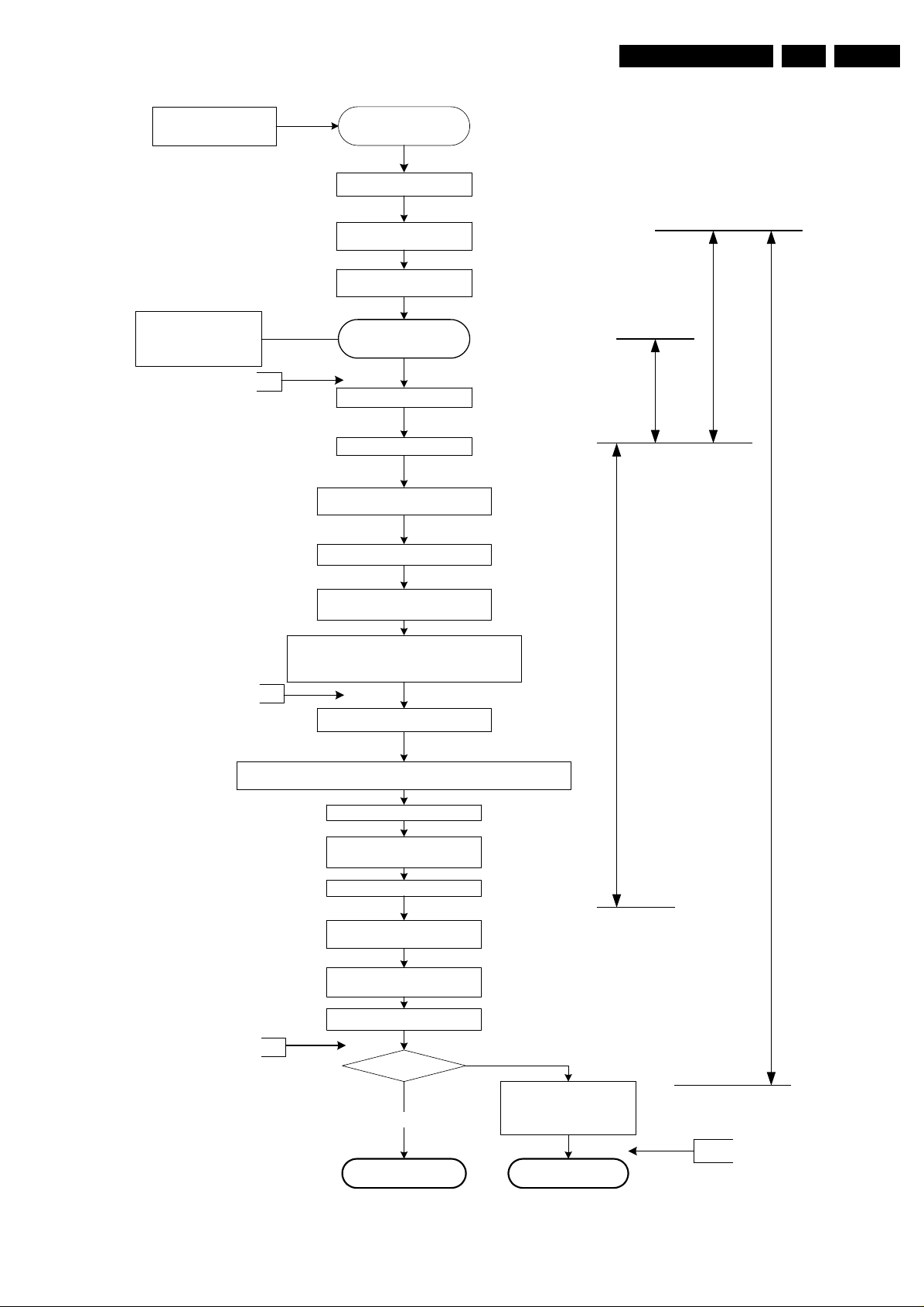
Service Modes, Error Codes, and Fault Finding
EN 25FTL13U AA & AB 5.
ON/OFF switch to ON
start time extraction
stand-by bit = off
Step 1
OFF
OTC gets supply voltage
OTC resets, Initialise IO
pins
Read NVM identification
enable watchdog
Stand-by
Activate MSP reset
Put Stand-by line LOW
Keep sound amplifiers muted with
sound enable = high
+5V and +8V is switched on
t<500ms
t<250ms
+8V and +5V get their nominal
level, detected by the OTC
Activate protection algorithms for +8V and +5V
and I²C (start I²C protection the moment the
component is initialised).
Step 2
Read rest of NVM information
Initialize HIP: IF, source selection, 2fh input, video processing
Switch on the syncoutput: set_syncout_tristate= off
Initialize tuner
Initialize 3D Combfilter (US
only)
Initialize PICNIC
Start time extraction
Deactivate reset MSP and
Initialize MSP
Initialize EPLD
t<1500ms
t>400ms
Step 3
Stand-by bit set ?
yes
Semi stand-by
no
Switch On PDP
Initialize PDP
Figure 5-1 Stepwise start-up diagram
ON
or
Step 5
CL 36532053_064.eps
221003
Page 26
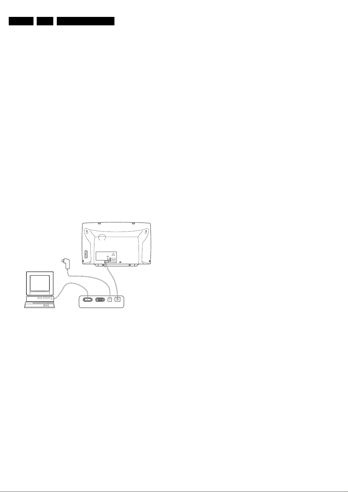
EN 26 FTL13U AA & AB5.
Service Modes, Error Codes, and Fault Finding
Note (*):
• When the set is in stepwise mode and, due to stepping-up,
a protection is activated, the set will really go into protection
(blinking LED). The set will not leave the stepwise-mode
however. If state X is the state where the set went to
protection, stepwise start-up will return to state X-1. At
state (X-1) diagnostic measurements can be performed.
Also, in the short time the set is in state X but not yet in
protection, you can also do some measurements.
5.4.4 How To Connect
1. First, install the ComPair Browser software (see the Quick
Reference Card for installation instructions).
2. Connect the RS232 interface cable between a free serial
(COM) port of your PC and the PC connector (marked with
“PC”) of the ComPair interface.
3. Connect the mains adapter to the supply connector
(marked with “POWER 9V DC”) of the ComPair interface.
4. Switch the ComPair interface “OFF”.
5. Switch the television set “OFF” with the mains switch.
6. Connect the ComPair interface cable between the
connector on the rear side of the ComPair interface
(marked with “I2C”) and the ComPair connector at the rear
side of the TV.
7. Plug the mains adapter in a mains outlet, and switch the
interface “ON”. The green and red LEDs light up together.
The red LED extinguishes after approx. 1 second while the
green LED remains lit.
8. Start the ComPair program and read the “Introduction”
chapter.
When an error occurs and the error buffer is full, then the new
error is not added, and the error buffer stays intact (history is
maintained), except when the error is a protection error.
To prevent that an occasional error stays in the list forever, the
error is removed from the list after 50+ operation hours.
When multiple errors occur (errors occurred within a short time
span), there is a high probability that there is some relation
between them.
5.5.2 How to read the Error Buffer
Use one of the following methods:
• On screen via the SAM (only if you have a picture).
Examples:
– 0 0 0 0 0: No errors detected
– 6 0 0 0 0: Error code 6 is the last and only detected
error
– 9 6 0 0 0: Error code 6 was first detected and error code
9 is the last detected error
• Via the blinking LED procedure (when you have no
picture). See paragraph "The Blinking LED Procedure"
further on.
•Via ComPair.
5.5.3 How to clear the Error Buffer
Use one of the following methods:
• By activation of the “RESET ERROR BUFFER” command
in the SAM menu.
• With a normal RC, key in sequence “MUTE” followed by
“062599” and “OK”.
• When you transmit the commands “DIAGNOSE” - “99” “OK” with ComPair (DST-emulation feature).
• If the content of the error buffer has not changed for 50+
hours, it resets automatically.
SERVICE
CONNECTOR
PC VCR I2CPower
Figure 5-2 ComPair Interface connection
5.4.5 How To Order
ComPair order codes:
• ComPair Software: ST4191.
• ComPair Interface Box: 4822 727 21631.
• AC Adapter: T405-ND.
• ComPair Quick Start Guide: ST4190.
Note: If you encounter any problems, contact your local
support desk.
5.5 Error Codes
5.5.1 Introduction
9V DC
L
R
AUDIO EXTERNAL 1
EXTERNAL 2
CL96532156_029.eps
190600
5.5.4 Error Codes
In case of non-intermittent faults, clear the error buffer before
you begin the repair. This to ensure that old error codes are no
longer present. Before clearing the buffer, write down the
content, as this history can give you significant information.
If possible, check the entire contents of the error buffer. In
some situations, an error code is only the result of another error
code and not the actual cause (e.g., a fault in the protection
detection circuitry can also lead to a protection).
There are various errors:
• I2C device errors.
• I2C bus errors.
• Protection errors.
• Errors not related to an I2C device, but of importance:
– FALCONIC (ERROR 26): at start-up, after initialization
of the PICNIC, the presence of the FALCONIC can be
checked.
– EAGLE (ERROR 27): at start-up, after initialization of
the PICNIC, the presence of the Eagle can be
checked.
The error code buffer contains all detected errors since the last
time the buffer was erased. The buffer is written from left to
right, new errors are logged at the left side, and all other errors
shift one position to the right.
When an error has occurred, the error is added to the list of
errors, provided the list is not full or the error is a protection
error.
Page 27
Service Modes, Error Codes, and Fault Finding
Table 5-1 Error Table
Error Device Description Def. item Def. Module indication Diagram
1 M24C32 NVM, spontaneous blinking error 1 7011 Control B5a
3 SAA4978 PICNIC 7713 Feature Box B3a
4 Supply 5 V 5V protection +5V Supply B5a
5 Supply 8 V 8V protection +8V Supply B5a
6 Slow I2C bus blocked Spontaneous blinking error 6 Slow I2C Blocked
8 TDA932x HIP High-end Input Processor 7323 Chroma IF IO B2
13 UV1318/... Tuner protection 1T01 Tuner B13
14 MSPxxxx ITT sound processor 7A02 Audio module B6a
15 UPD64083 3D Comb 7B00 Video controller B11
18 Fast I2C bus blocked Spontaneous blinking error 18 Fast I2C Blocked
21 M62320P I/O Expander 7P56 Video Dual Screen B15b
26 SAA4992 Falconic 7718 +3V (FBX) Supply B3b
27 T8F24EF Eagle 7724 +3V (FBX) Supply B3c
32 M29W400BT Flash Ram (EPG) 7012 EPG Memory B5a
53 AD9883A AD converter 2fh input 7L01 HD B19c
55 DC/DC converter One of the voltages is not ok + protection error Supply
56 EPLD EPLD error 7V01 Video control B19d,f
76 - Audio DC protection - - A
83 TEA6422 Source select matrix audio 7I17 Audio Source Select B14d
EN 27FTL13U AA & AB 5.
Note: Error codes 1, 6, or 18 are protection codes and in this
case, supplies of some circuits will be switched “OFF”. Also, in
protection, the LED will blink the number of times equivalent to
the most recent error code.
5.6 The Blinking LED Procedure
5.6.1 Introduction
Via this procedure, you can make the contents of the error
buffer visible via the front LED. This is especially useful for fault
finding, when there is no picture.
When the SDM is entered, the front LED will show (blink) the
contents of the error-buffer. Error-codes > 10 are shown as
follows:
– A long blink of 750 ms (which is an indication of the decimal
digit),
– A pause of 1.5 s,
– “n” short blinks (where “n” = 1 - 9),
– When all the error-codes are displayed, the sequence
finishes with a LED blink of 3 s,
– The sequence starts again.
Example: Error 12 9 6 0 0.
After activation of the SDM, the front LED will show:
– 1 long blink of 750 ms (which is an indication of the decimal
digit) followed by a pause of 1.5 s,
– 2 short blinks followed by a pause of 3 s,
– 9 short blinks followed by a pause of 3 s,
– 6 short blinks followed by a pause of 3 s,
– 1 long blink of 3 s to finish the sequence,
– The sequence starts again.
Note: If errors 1, 6, or 18 occur, the LED always gives the last
occurred error even if the set is NOT in service mode.
5.6.2 How to Enter
Use one of the following methods:
• Enter the SDM (only via soldering pads marked “SDM” on
SSP). The blinking front LED will show the entire contents
of the error buffer (this works in “normal operation” mode
and in “protection” mode).
• Transmit the commands “MUTE” - “062500” - “OK” with a
normal RC. The complete error buffer is shown. Take
notice that it takes some seconds before the blinking LED
starts.
• Transmit the commands “MUTE” - “06250x” - “OK” with a
normal RC (where “x” is a number between 1 and 5). When
x= 1 the last detected error is shown, x= 2 the second last
error, etc.... Take notice that it takes some seconds before
the blinking LED starts.
• “DIAGNOSE X” with the DST-emulation feature of
ComPair (where “x” is a number between 1 and 5). When
x= 1 the last detected error is shown, x= 2 the second last
error, etc.... When x = 0 all errors are shown.
5.7 Protections
5.7.1 Introduction
This chassis has only one microprocessor (OTC), which
remains active during Standby. This because power of the
microprocessor and the attached memory chip set is coming
from the 3V3 supply, which is derived from the 5V Standbycircuitry. Therefore, in both Power-on as in Standby “power-off”
mode, the microprocessor is connected to this power supply.
If a fault situation is detected, an error code will be generated
and if necessary, the set is put in protection mode. The
protection mode is indicated by the blinking of the front LED at
a frequency of 3 Hz (or by a coded blinking in special cases).
The content of the error buffer can be read via the service menu
(SAM), the blinking LED procedure or via DST/ComPair.
To get a quick diagnosis, this chassis has three service-modes
implemented:
• The Customer Service Mode (CSM).
• The Service Default Mode (SDM). Start-up of the set in a
predefined way.
• The Service Alignment Mode (SAM). In this mode, items
of the set can be adjusted via a menu.
You can enter both SDM and SAM modes via the “service
pads” on the SSP, via an RC-transmitter, or via ComPair. It is
not possible to enter the SAM in “standby”; the TV has to be in
“normal operation” mode.
The “Protection Diagram” shows the structure of the protection
system. See diagram below.
Page 28

EN 28 FTL13U AA & AB5.
Service Modes, Error Codes, and Fault Finding
5.7.4 Hardware Protection
TUNER
FAST I2C BUS BLOCKED
SLOW I2C BUS BLOCKED
EPLD
+
FBX
+
3D COMB (US)
DC_PROT (from audio)
+8V_CON
+5V_CON
DC/DC
PROTECTION
IRQ-DIGITAL (98)
+8V SENSE (105)
+5V SENSE (106)
I2C
Figure 5-3 Protection diagram.
There are several types of protections:
• I2C related protections.
• OTC related protections (via polling on I/O pins or via
algorithms).
• Hardware protection
All protections are explained below.
5.7.2 I2C Related Protections
In normal operation, some registers of the I2C controlled ICs
are refreshed every 200 ms. During this sequence, the I2C
busses and the I2C ICs are checked.
An I2C protection will take place if the SDA and SCL lines are
short-circuited to ground, or to each other. An I2C error will also
occur, if the power supply of the IC is missing.
DC/DC protection
When a 3V3 supply is short-circuited the DC/DC converter
switches off and goes in protection. The FBX, EPLD IC, and
3D comb IC have no supply voltage and give no acknowledge.
In this case, the set should go into protection. An error code is
written in the NVM: DC/DC error.
FBX protection
The FBX protection is not available any more. It is replaced by
the DC/DC protection.
5.7.3 OTC Related Protections
If a protection is detected at an OTC input, the OTC will start to
scan all protection inputs every 200 ms for 5 times. If the
protection on one of the inputs is still active after 1 s, the
microprocessor will put the set in the protection mode. Before
the scanning is started, a so-called “ESD refresh” is carried out.
This is done, because the interrupt on one of the inputs is
possibly caused either by a flash or by ESD. As a flash or ESD
can influence IC settings, the HIP, MSP, 3D Comb and wireless
module (not used in this set) are initialized again, to ensure the
normal picture and sound conditions of the set.
OTC
CL 36532053_065.eps
100703
Short-circuiting the 3V3 supply from the DC/DC converter will
shut down the DC/DC converter. The absence of the 3V3
supply line is also sensed via I2C (see description DC/DC
protection above), this is useful if there is something wrong in
the detection circuit of the DC/DC converter. There are no
hardware protections in this chassis, which switch off the
supply.
5.8 Repair tips
5.8.1 3V3 Supply (DC/DC converter)
As mentioned above, the DC/DC converter is switched “off”
when something goes wrong (detection of a missing 3V3
supply at one of the devices supplied by the 3V3). Because of
this, the set goes to protection (I2C protection). Error code 55
is logged.
For further diagnoses, you need to overrule the I2C protection:
put the set in Service Default Mode by means of the solder
pads on the SSB.
The DC/DC converter is still not working because it is switched
“off” by the 3V3_FAULT line (schematic B12). Now you have
some possibilities:
1. First, measure the impedance over diode 6U06. In normal
conditions, you should measure approximately 120 ohm (if
possible, verify this with another set). If the impedance is
much too low, do not try to start up the converter as
mentioned below. Remind that if FET 7U03 is shortcircuited, this will also influence your measurement.
2. Desolder coils 5U05 and 5U06, connect an external 3V3
supply at capacitor 2U23 (current limitation to 500 mA) and
a second external 3V3 supply at capacitor 2U31 (current
limitation to 800 mA). The normal working current of the
3V3_SIM line is approximately 400 mA and the normal
working current for the 3V3_DCDCFBX line is
approximately 700 mA. Therefore, if one of the currents
exceeds their nominal value you can determine in which
circuit the overload is situated. If the set would start up and
you have normal picture, there is probably no overload but
a problem in the detection circuits.
3. If you do not have two external power supplies, you can do
the following: Desolder coils 5U02, 5U03, and 5U04 (you
must desolder all three, otherwise the circuit could be
damaged), connect an external power supply of 3V3 at the
cathode of diode 6U06. Make sure to limit the current of this
external supply to approximately 1200 mA. If the supplied
current exceeds 1100 mA (approximately normal working
current) you can conclude that one of the devices supplied
by 3V3 is short-circuited.
4. Another possibility is to force the converter to start up by
short-circuiting (and keep short-circuited) resistor 3U25
(B12).
Caution: Be aware that this can damage the set. Even if
you measure approximately 120 ohm over diode 6U06,
there can still be something wrong in the converter itself.
By short-circuiting resistor 3U25, the internal protection of
the converter is disabled.
8 V and 5 V protections
The microprocessor senses the presence of the 8 V and 5 V
(via the “+5V_CON” and “+8V_CON” lines). If one (or both) of
these voltages is (are) not present, an error code is stored in
the error buffer of the NVM, and the set is put in the protection
mode.
Audio DC protection
The OTC senses if the audio module is in protection via IRQDIGITAL (pin 98 of OTC). If this is the case, the OTC puts the
set in protection.
5.8.2 ComPair
This chassis does not have an IR transmitting LED (as in MGsets). Therefore, a “Service” (ComPair) connector is
implemented at the bottom of the set, which is directly
accessible. In addition to this, there is also a blinking LED
procedure to show the contents of the error buffer.
When you use ComPair, you have the possibility to activate a
“stepwise start-up” mode. With this mode, you can initiate the
start-up sequence step by step. This also means that in certain
steps, some protections are not activated. This is sometimes
very convenient during repair.
Page 29
Service Modes, Error Codes, and Fault Finding
EN 29FTL13U AA & AB 5.
5.8.3 Protections
Activating SDM via the “service pads” will overrule the
processor-controlled protections, but not the hardware
protections. This means, that the A/D-input protections (5 and
8 V) and the I2C “not-acknowledging” info of FBX + EPLD + 3D
Comb and of the tuner are overruled.
Caution: When doing this, the service technician must know
what he is doing, as it could lead to damaging the set.
Table 5-2 Repair tips
Phenomenon Possible Cause Repair tips
No picture, LED blinking at
3 Hz.
No picture, LED blinking
with code 6-6-6 or 18-18-
18.
No picture, LED blinking
with code 1-1-1.
No RC-reception. LED does
not echo RC-commands.
Picture is not synchronised. The sync is derived in the HIP. Check crystals in the HIP circuit on bad contacts.
Picture is distorted. Check video-path in Service
Picture with horizontal
stripes.
No menu, no OSD. Probably a defective uP. Measure test points B61to B64 on diagram B5A.
No NextView (EPG). IC7012 defective or not pow-
No Teletext. IC7007 defective or not pow-
Various symptoms, due to
missing local supply voltage.
For ITV (Institutional TV)
models, it is possible that
the service modes are not
functioning as expected.
Set is in protection due to various causes. For error codes
see error-code list.
No communication on slow I2Cor fast I2C-bus.
No communication on NVM-I2C
bus to the uP.
uP circuitry or RC-receiver is
defective.
Default Mode.
Pixel Plus processing is malfunctioning
ered.
ered.
An interrupted fuse, NFR-resistor or connection.
"Hotel Mode" option is set to
"ON". This can cause problems
with service modes.
5.8.4 Power Supply
The simplest way to repair the power supply is to check (and
replace if necessary) the components that are marked gray on
schematic SP1.
5.8.5 AUX Supply
First determine whether one or more of the secondary diodes
(6044, 6021, 6291, 6293) are short-circuited. If this is not the
case, check (and replace if necessary) the components that
are marked gray on schematic SA.
You have no picture, so:Read the error buffer via ComPair (error buffer is accessible when set is in protection, compare-file will guide you to this)- Read the
blinking LED information via standard remote command <mute>06250x<ok>.-
Or you read the error code sequence via standard remote command
<mute>062500<ok>. When you have found the error, check the circuitry related to the supply voltage and I2C-communication or the circuitry that triggers
the protection.
As processor cannot communicate with one of the 2 busses it the standby-led
spontaneously starts blinking 6-6-6-etc or 18-18-18-etc... If in the error buffer
somewhere is an error 6 or 18, these will have the highest priority starting the
mentioned blinking. Measure dependent of the error on the I2C-bus which device is loading the bus. (Use I2C-overview)
As the uP cannot communicate with the NVM I2C bus, it spontaneously starts
blinking 1-1-1.
Note: when there is no access to the NVM, a lot of picture setting can go
wrong.
In case the set does react on a local keyboard operation, you must check the
RC-receiver circuitry (diagram LD).
Investigate whether there is an error code present in the error buffer. In case
there is one, check the I2C-bus and/or supply lines (see overview supply
lines).Measure and check signal path Tuner-HIP-FBX-EPLD.
Check functionality on circuitry (B3a, B3b, and B3c) of PICNIC (7713), FALCONIC (7718, EAGLE (7724) and/or field memories (7714, 7717, 7719, 7722
and 7723.Tip: the whole Pixel Plus chipset (3 ICs + 5 Field Memories) can be
diagnosed via ComPair.
Check circuitry around IC7012 on diagram B5A.
Check circuitry around IC7007 on diagram B5A. Check also B61 to B64
around uP on diagram B5A.
When no symptom or error code leads you to a specific circuitry, use the supply lines overview (see supply lines overview), for a quick scan of all supply
lines.
Switch "OFF" the "Hotel Mode" option, in "Service Alignment Mode", "Service
Options", "Miscellaneous", "Hotel Mode". After repair this option should be
switched on again to use Hotel Mode functionality.
5.9 Software Downloading
In this chassis, you can upgrade the software via ComPair
without removing the back cover of the set. The switch, which
is needed for the software downloading procedure, can be
reached through the cooling gaps of the back cover. The switch
is located next to the SAM/SDM pads and can be operated with
a long and thin screwdriver. Make sure that you do not damage
the PWB with sharp objects. You can find more information on
how this procedure works in the ComPair file. It is possible that
not all sets are equipped with the hardware, needed to make
software upgrading possible. To speed up the programming
process the firmware of the ComPair interface can be
upgraded. See paragraph “How To Order” for the order number
Page 30

EN 30 FTL13U AA & AB5.
Personal Notes:
Service Modes, Error Codes, and Fault Finding
E_06532_012.eps
131004
Page 31

Wiring Diagram, Block Diagrams, and Overviews
6. Wiring Diagram, Block Diagrams, and Overviews
Wiring Diagram
31FTL13U AA & AB 6.
LSP
HIGH
R
Backlight
Supply
Connector
16P
0304 0303
4P 4P
Audio
A
Amplifier
Class D
amplifier
8P
9P
0388
0302
9P
1302
16P
1313
16P
LCD Panel
1345
3P
1312
20P
nn
LVDS
Connector
8301 8355 8346
P
5P
1370
Topcontrol
SA
9P
1355
Aux Supply
nn
5P 7P
1346
1333
8333
2P
1309
2P
1309
LCD PanelLCD Panel
LSP
HIGH
L
LD
6P
0317
LSP
R
LOW
LSP
R
LOW
Mains
switch
10P
LCD Panel
0320
ONLY FOR ITV MODEL
Backlight
Supply
Connector
11P
Side I/O
O
0936
16P
CN1CN1
6P
1903
1Y45
3P
5P
1I70
B
1Y01
SSP
20P
8370
1Y55
9P
8P
5P
11P
10P
1S20
1S88
1S361S46
MAINS
SP
7P
1333
Power Supply
2P
1308
LSP
L
LOW
LSP
L
LOW
CL 36532064_045.eps
301204
Page 32

Wiring Diagram, Block Diagrams, and Overviews
32FTL13U AA & AB 6.
Block Diagram Supply and Supply Lines
RECTIFIER / DOUBLER
SP2
6807
GBJ6J
SP1
0308
2
1
3507
LD
+5V-STBY-SW
+
-
7805 (str83145)
7801 - 7803
VOLTAGE
DOUBLER
(for 110V only)
POWER SUPPLY
1400
T3.15AH
6506
DF06M
-
CONTROL
7500
TNY266
4
ENABLE
SWITCH PANEL
+8V6
+9V-STBY-SW
+9V-STBY
1101
1
4
2
5
ON
3
6
400V-HOT
5401
5403
MAINS
FILTER
+
DRAIN
SOURCE
TCET1102
0320
5100
10
ON / OFF
SWITCH
5
7-8
7501
6
8
9
1309
1
2
5500
2
3
4
3
HOT COLD
SA
1309
1
3
7017
7018
23
7460
7505
6
7
8
9
1
2
B1
1S20
6
8
9
10
AUX SUPPLY
5003
2001
SOFT
START
+
CURRENT
PROTECTION
1450
14
RELAY
CONTROL
6515 6516
6505
3501
7502
TL431
5S03
5S08
+5V-SW
2510
1
3
2
2x
3028
3031
3032
7001
MC34067P
11
OSCC
3007
CONTROL
7
ERROR
11
SOST
7003
7004
VOLTAGE
PROTECTION
HOT COLD
STANDBY SUPPLY
7503
7504
2510
3505
3503
STANDBY
V TUN
+5V-SW
+5V2
+5V2-RELAY-IO2
POR
+5V2-RELAY-IO2
+5V2
OVER
POR
CIRCUIT
6503
+8V
VCC
OA
OB
BIAS SUPPLY
15
14
12
10
FI
6504
7531
STD16NEO6L
D
G
7506
7507
7532
SWITCH
CONTROL
1333
1
2
3
4
5
6
7
2x
S
5001
4
2
1333
1
2
3
4
5
6
7
B11
+3V3-SIM
3000
3D COMB
7007
7020
HIGH
10
SIDE
DRIVE
11
7008,
7021, 7022
LOW
14
SIDE
DRIVE
13
+5V2-RELAY-IO2
+5V2-RELAY-IO2
5B06
1
2003
STU16NB501
STU16NB501
G
POR
V TUN
+5V2
+5V-SW
STANDBY
+5V2-RELAY-IO2
7B07
60786079
G
STANDBY
+5V-SW
3
7005
7006
S
V TUN
+5V2
POR
9B01
5B07
PCET1102
D
S
D
BACKLIGHT-CTRL
2x
POR
LIGHT-ON
2x
STANDBY
1x
DC-PROT
+5V2-RELAY-IO2
1x
+5V2
V TUN
+12V
+5V2
+8V6
+12V
-5V-SW
1x
1x
3x
1x
5040
3V3 IO
2V5D
2V5A
2V5C
7003
8
7
3
5
4
3
HOT
COLD
COLDHOT
5002
2
9
10
11
12
13
14
15
16
B19B
3057
1
1005
T5A
1006
T5A
5025
5026
N.C.
TEMPERATURE
DVI RECEIVER
6044
STPS20L40CFP
3
1
6021
STTH2003C
1
3
SENSOR
+3V3-AD
5V25
5V21
5V30
3030
2
2
T+
3072
1370
3022
+12V
+24V
7210
TL431CZ
1355
1
2
3
4
5
6
7
8
9
1
2
3
4
5
1346
1
2
3
4
5
3V3-AD
3V3-SI-IO
VCC-SI
3V3-TMDS
3052
3024
VS Voltage
Adj.
3026
B20
1Y55
BACKLIGHT-CTRL
1
2
3
4
5
6
7
8
9
B14A
1I70
1
2
3
4
+5V2
5
B1
1S46
1
2
3
4
5
1007
T5A
IN
POR-IO2
LAMP-ON
FAN-SPEED
STBY-TEMP
DC-PROT-IO2
+5V2
+8V
+11V
+5V
AUDIO SUPPLYVS SUPPLY
6293
6291
+5V2 (T0 3300)
7011
L4940
3IK7
5S02
5S01
5S04
5S05
5S03
VSND-NEG
VSND-POS
+5V2
DC-PROT
DC-PROT
+5V2
+12V
+8V6
OUT
+24V
B5B
B1
B19F
N.C.
N.C..
STANDBY-IO2
B1 B5A
+5V2-RELAY-IO2
+5V2
+33V
+11V
+8V
+8VA
+8VA
+8V-AUD
+8V-VDP
+5V-CON
+5V-VDP
+5V-AUD
+8V
+5V
1302
1
2
3
4
5
6
7
8
9
1x
2x
1x
2x
+3V3-SIM
+3V3-AD
SUPPLY & DC PROTECTION
A7
0302
1
2
3
4
5
6
7
8
9
B12
+11V
+5V2-RELAY-IO2
+5V2_CON
1x
+8V
+8V_CON
2x
+5V_VDP
+8V_VDP
1x
1x
+8V_VDP
3x
+5V_VDP
1x
B5A
+8V_CON
1x
+5V2_CON
2x
4x
+5V_CON
1x
7x
B6A
3x
+5V_AUD
2x
1x
+8V_AUD
+5V
+5VF
1x
+11V_S
B5B
+5V_CON
B13
B14C
+5V
+8VA
B14D
1740
5725
2A5
1730
5335
2A5
DC-PROT
DC/DC CONVERTER
T800mA
CONTROL
IF / IO
B2
HOP
B4
OTC
AUDIO DEMODULATOR
BACKLIGHT CONTROL
TUNER
+5V
+33V
2FH I/O
AUDIO I/O
+5V
+8V
7745, 7746
STAB
7735, 7736
STAB
+11V
1U01
+3V3_FAULT (x lines)
IN
+5V
1403
F500mA
7005
3IN4
5U02
7U04
G
7U03
G
5415
5416
3402
3400
3304
OUT
5A00
5A03
3A03
5A06
5A01
VSDN-NEG
Vcc-10-NEG
VSDN-POS
Vcc-10-POS
+9V-STBY
D
S
D
S
+8V_CON
+5V2_CON
+3V3_INTOTC
+5V_CON
+5V_CON
+5V
+33V
+5VIO
+8VA
+5V
+8V
5U01
+5V2_CON
+8V_CON
+5VCOM
+8VP
+8V_VDP
+5VS
+8V_VDP
+5V_VDP
+5VS
+5DA
+5DB
+8V-AUD
+8VC
+5VF
+11V_AUD
6U02
5U05
5U06
+8Vp
9,19,20,
38,49,
75,101,
SAA5801H
A2
5404
11
7323
TDA9320H
HIP
+5VCOM
7307
TDA9181
111
7001
OTC
7A02
MSP3
AUDIO
PROC.
FILTERS
Vcc-10-NEG
Vcc-10-POS
+9V-STBY
+3V3_LINK
+3V3_SIM
+3V3_DCDC FBX
+3V3_DCDC FBX
+3V3_SIM
5405
45
6.5
B5B
B5C
B1
104
31
A3 A6
VSDN-NEG
Vcc-10-NEG
VSDN-POS
Vcc-10-POS
N.C.
+5V-CON
OTC-FLASH
+3V3_INTOTC
STANDBY-IO2
:
+24V
LIGHT-ON
BACKLIGHT
CTRL
+24V
LIGHT-ON
BACKLIGHT
CTRL
I/O EUR
B14B
+5V2
+5V
+11V
3IC1
+5V
3IB4
7I09
3IB5
1x
PIP IF I/O
B15A
2x
B15B
B19F
+8V
+5V
+3V3-EPLD
I/O
EPLD
5P01
5P51
3P02
B19A
3D73
+8V
B19C
+5V
+3V3-I2C
1x
B19D
1x
+3V3-SIM
+3V3-AD
1x
+3V3-EPLD
1x
+3V3-I2C
B19E
+5V
5D51
3D81
6D93 6D64
HD1 A/D CONVERTER
7L02
5L07
5L13
5L09
5L14
5L11
5L15
EPLD CONTROL
5E53
7E05
3
1
EPLD OSD
3E08
5E08
3E04
5E04
7I07
5D54
5E59
5E51
5E50
+5V2
+5V
+11V
+11V_S
+11V_S
+8VIPP
B20
1x
+11V
+3V3-EPLD
LCD-PWR-ON
7Y00
IRFR9024N
3
1
7Y01
+12V-LCD
2
3Y03
3Y04
B19F
+5VD
B3A
+5VF
+5VA
1x
+3V3-EPLD
+3V3
_DCDC FBX
+2V5B
2x
+8-VIDEO
REF3
6D62
REF2
REF1
+3V3-I2C
VD
VD-1
VDD
VDD-1
PVD
PVD-1
+3V3-AD
+3V3-EPLD
+3V3-AD
+3V3-IO
+1V5
+1V5-PLA
+3V3-I2C
+5VA-OSD
+VT
3
4
7E24
5
+VB
3E45
+3V3_FBX
3x
+3V3A
1x
+3V3_INT
1x
B3B
+3V3_FBX
+2V5B
+3V3_INT
+3V3_FBX
B3C
+3V3_FBX
+5VA +5VA
+2V5B
+3V3A
+8V_CON
PICNIC
FALCONIC
EAGLE
5756
5744
5747
5746
5719
5718
5753
5716
5717
+5VA
5748
5721
+3V3A
+8V_CON
5706
+3V3_FBX
+3V3_FBX
+3V3FA
+3V3_FAULT
+2V5FB
+3V3_INT
To 7717
+3V3_FAULT
To 7719
+3V3_FAULT
5725
5722
B12
B12
B12
+2V5_E
+2V5FCA
+2V5FCD
5742
1312
1-6
12
13
14
1313
1-6
12
13
14
1Y01
LCD
DISPLAY
3
4
5
6
7706
5729
5731
5737
5713
B3D
5745
5738
5724
5727
5726
7727
BACKLIGHT
CONNECTOR
BACKLIGHT
CONNECTOR
LVD S
CONNECTOR
+5VA
+2V5B
5714
11-7713
5736
24-7713
+3V3A
+3V3_INT
+3V3FM
+3V3P
2FH INTERFACE
+3V3_FBX
7726
5743
5728
CL 36532064_044.eps
+3V3_E
+3V3FCD
+3V3FC1
+3V3FC2
+1V5_E
+1V5FCA
+1V5FCC
061003
Page 33

Wiring Diagram, Block Diagrams, and Overviews
33FTL13U AA & AB 6.
Testpoint Overview Aux and Power Supply
SA AUX SUPPLY (TRACK SIDE VIEW) SP POWER SUPPLY (TRACK SIDE VIEW)
19
1312
1355
1370
5
1
7011
OUT
G
IN
6021
3
2
6293
6044
2
1
3
1
A
K
+24V
1313
1
1
+12V
VS
+
Adj
1
3026
1346
1
5
1333
7
1
5002
MAINS
TRAFO
1309
400V_HOT
7005
S
D
116
89
G
5
5001
DRIVER
1
7006
S
D
10
6
2
1
G
6807
1309
400V_HOT
1
2
HOT
COLD
1302
169
9
6291
A
K
COLD
HOT
7001
CONTROL
18
+
7500
CONTROL
41
5
58
1
6
5500
9
7531
SG
D
+5V_SW
1333
1
7
1400
FUSE
0308
12
MAINS INPUT
COLD
HOT
CL 36532053_069.eps
180703
Page 34

Block Diagram Video
VIDEO
TUN1
B13
+33V
+5V
5T02
6TO8
9
7,3
1
ERR
13
4
15
AGC1
S-SDA
S-SCL
Y-CVBS-SC2-AV2-IN
C-SC2-SVHS-IN
CVBS-SC2-MON-OUT
R/G/B-SC1-Y/U/V-IN
-/33
T1
11
1TO1
UV1318ST
TUNER
1
2
3
4
5
6
CVBS-SC1-AV1-IN
CVBS-AV3-IN
Wiring Diagram, Block Diagrams, and Overviews
IF, I/O VIDEOPROCESSING
B2
IF-TER
AGC
MONITOR
B5A
1410
SAW FILTER
VIDEO
VIF1
VIF2
TUNER AGC
SIF2
SIF1
1411
SOUND BANDPASS
4.5 MHz
I5
7411
62
64
63
7323
TDA9320H
2
3
7410
1406
SOUND
FILTER
4.5 MHz
I6
10 12 13 14
PLL
DEM
QSS
QSS-AM
MIXER
AM
DEMO
QSS-AM
GROUP
DELAY
COR.
5
7322
HIP
ERR
SEE
B6A
BLOCK DIAGRAM
AUDIO
Y-CVBS-FRONT-IN
C-FRONT-IN
7415
B5A
7320
V2
8
OTC
Y5
16
18
20
21
23
24
CVBS-TXT
12
VIDEO
SWITCH
CONTROL
26 29
+
B11
7B09
28
CY
Y
C
SYNC
SEPAR.
32
34
N.C.
3D-COMB
88
Y
PROC.
C
PROC.
R
SCART1
36 37 38 39
7B00
UPD64083CF
3D-COMB
COUT-3D-COMB
YOUT-3D-COMB
Y/U/V
SWITCH
UU
DECODER
PAL
NTSC
SECAM
H-SYNC
PROC.
V-SYNC
PROC.
RGB/YUV
MATRIX
G B
84 Y
C
83
Y
U
V
VY V
V
UY
R G B
41 42 43 40
N.C.
7B10
7B02
YOUT-3D-COMB
COUT-3D-COMB
49
50
51
60
61
1308
57
46
47
SCART2
7414
V7
V8
L8
F14
NTSC M
3.57MHz
SCL-F
SDA-F
B6A
V6
9A04
Y50
U50
V50
HA50
VA50
Y-PIP+MAIN-OUT
9A05
U-PIP+MAIN-OUT
9A06
V-PIP+MAIN-OUT
HA50
7740
24
1
7741
24
1
VREF
VA
23145
SWITCH_2FH
SWITCH_1FH
B3A
3727
3722
34FTL13U AA & AB 6.
PICNIC
L6
L7
L8
L10
L11
SCL-F
SDA-F
INTR1
64K
7711
PROM
M27C512
7713
SAA4978H
23
3x
ADC
25
26
PICNIC FALCONIC
28
29
4
5
74HC573D
LATCH
DIGITAL
SIGNAL PROCESSING
ERR
3
SYNC PROCESSING
7712
7714
MS81V04160
DA (0-15)
FIELD
MEMORY
FM1
CLI6
WEC
RSTW
RSTR
RNRST
SNDA
SNCL
REF
1
SNDA
21
2
SNCL
Href-EXT
30
12
CLK 32P
89
13(2x)
12,21
MF (1-17)
FEA
B3B
FALCONIC
7718
SAA4992
7717
MSM54V12222A
FIELD
MEMORY
2
ERR
26
7717
MSM54V12222A
FIELD
MEMORY
3
B3C
Y-2FH (0-7)
UV-2FH (0-7)
YF (0-7)
UVF (0-7)
EAGLE
Y-2FH (0-7)
UV-2FH (0-7)
B3D
7743
7745
7742
7744
BUFFER
BUFFER
BUFFER
BUFFER
2FH INTERFACE
(BUFFERS)
YF-BUFF (0-7)
UVF-BUFF (0-7)
2,5,11,18,
19,20,23
7722
MS81V04160
FIELD
MEMORY
FM4
(lower lines)
7723
MS81V04160
FIELD
MEMORY
FM5
(lower lines)
18
19
20
2
5
11
23
YGO (0-7)
UVGO (0-7)
YGO (0-7)
HVGO (0-7)
CLK32I
FALREF
REFIN
Vref
INSTR1
SNDA
SNCL
Href
CLK32E
7724
TBF24EF
EAGLE
ERR
27
Y-OUT (0-9)
U-VOUT (0-9)
RSTR
CLK64
HD-E
VD-E
CLOCK 32O
17
16
14
15
22
SIDE I/O
O B1 B14A
SVHS
251
CVBS
B14B
3
4
2
5
1
6
IN-Y-CVBS-SC2-AV2
IN-Y-CVBS-SC2-AV2
SC2-R-C-IN-AV2
AV3-CVBS-IN
SC2-CVBS-MON-OUT
IN-CVBS-SC1-AV1
DVI RECEIVER
B19B
1V21
DVI-D CONNECTOR
17
18
9
DVI-SIGNALS
7V26
M24CO1
EDID
16
24
NVM
C5
2FH I/O
B14C
Y-2
AV4
Pb-2
Pr-2
R/G/B-SC1-Y/U/V-IN
34
I/O US
C/16:9
Y
SVHS
MON-OUT
7557
SII905
DVI
RECEIVER
EPLD CONTROL
B19D
Y
2
4
C
7
AV1
SC1-CVBS
AV2
34
2
1
5
AV3
D7
18
D8
D11
D9 D10
1FH
H-DVI
V-DVI19
R-DVI23
G-DVI26
B-DVI31
2 Y-CVBS-FRONT-IN
C-FRONT-IN
4
7
B15B
S-SDA
S-SCL
B14C
SC1-CVBS
12
13
Y-2
B19A
7D52
7D53
7D54
Y-2
7126:7131
YPbPr/
YUV
MATRIX
SC1-R-IN-V-IN
SC1-G-IN-Y-IN
SC1-B-IN-U-IN
I/O
7P56
M62320
3
2
7132
74HC4053
3
5
1
2
9I01
9I02
OPTIONAL
7P51
Z86130
S-SDA
14
9
I/O
EXP
10
11
ERR
??
12
4
15
14
11
DVI/RGB HDI A/D CONVERTER
R-VGA-BUF
G-VGA-BUF
B-VGA-BUF
SUB-Y-2FH
SUB-U-2FH
SUB-V-2FH
S-SCL
SWITCH-HEF
RGB/
YUV/
MATRIX
V-CHIP
15
3
5
B19C
7L03
SDA-F3
H-DVI
V-DVI
SUB-Y-2FH
RGB/YPbPr
OUTPUT SELECTION
SCL-F3
5
Y-V G A
U-VGA
V-VGA
U-VGA
SUB-U-2FH
Y-V G A
SUB-Y-2FH
V-VGA
SUB-V-2FH
2
6
3
7
4
8
15
16
7D51
TDA8601T
CLAMP
CLAMP
CLAMP
CLAMP
CLAMP
CLAMP
3-STATE
3-STATE
3-STATE
3-STATE
9
CLK-2FH
13
CLK-32P
H-2FH-AD-OUT
6
V-2FH-AD-OUT
7
SYNCDET
8
B19D
7E02
EPCS1
2
EPLD
FLASH
6
RAM
SERIAL
POWER
MAN.
SYNC
PROC.
CLOCK
ERR
53
A/D
H-DVI-BUF
+
66
H-2FH-AD-OUT
64
V-2FH-AD-OUT
+
65
SYNCDET
67
CLK-2FH
2-9
Y-AD (0-7)
70-77
UV-AD (0-7)
12-19
U-AD (0-7)
SELECT-VGA-YPBPR
7L01
AD9883AKST
57
REGISTER
56
30
31
49
GENERATOR
12
U-2FH
11
Y-2FH
COVERTER
10
V-2FH
13
26
1
12
14
15
2,3,4,13,16,17,
19,20,21,212,23,26
9, 10
26
6
7
8
9(2x)
10
Href-EXT
VA
Href-EXT
HD-E
VD-E
DATA
CLOCK
2FH . 3FH
1936
1936
7V01
EP1C12Q240C0
SWITCH
STANDARD
DEFLECTION
CONTROL
CONTROL
18
22
13
3
18
22
AND SUPPLY
CLOCK
SYNC
INPUT
313
B3D
SWITCH-2FH
CLK-32I
CLK-32O
CLK-32I
PWR-OK-PDP
LCD-PWR-ON
LAMP-ON
SELECT-VGA-YPBPR
Vref
Href
RSTR
REF
FALREF
REFIN
SWITCH-1FH
SWITCH-2FH
HD3-OTC
VD-OTC
16,17,18,19,20,21
2FH INTERFACE
(ZERO DELAY BUFFER)
+
B19F
SUPPLY
16
2,3,4,9,10,11,
7747
2
4
1
7748
24
1
EPLD I/O+ LVDS
CLK-2FH
9
CLK-64
18(2x)
CLK-VID
10
2(2x)
SDA-F3
11
17
SCL-F3
21
SN-CL
19
20
SN-DA
4
3(2x)
2
1
7746
CY23S02
IN
FBIN
Y-2FH (0-7)
UV-2FH (0-7)
UV
CONVERTION
CLKP
1:2
3704
3703
CLK-OSD
HD3-EPLD
VD-EPLD
B3A
23
EPLD
ERR
56
U-AD (0-7)
TO OTC
B5A
SEE ALSO
BLOCK DIAGRAM
CONTROL
UV-AD (0-7)
PATH
FOR
1FH, 2FH
ONLY
Y-AD (0-7)
PATH
FOR
3FH
ONLY
Y-OUT (0-9)
UV DEMUX
CONTRAST
SATURATION
BRIGHTNESS
U-VOUT (0-9)
CLKP
R (0-7)
YUV
to
RGB
R-OSD (0-5)
OSD
INSERTION
G-OSD (0-5)
B-OSD (0-5)
45 25
55 27
54 28VS-OUT
49 30DE-OUT
50 31CLK-OUT
53 32LVDS-PWR-DOWN
BL-OSD (0-4)
PARITY
HS-OUT
G (0-7)
B (0-7)
7V02
DS90C385MTD
PARALLEL
transmitter
HD3-OTC
LVDS
LVD S
+3V3-EPLD
1
48
47
TTL
46
to
45
42
41
38
37
40
PLL
39
OSD
OTC
B5A B3A B19E
EPLD
OSD
8
CLK-32ECLK-32P
OUT
38483855
7001
SAA5801H
77 R-TXT 2FHR-GFX R-OSD
78 G-TXT 2FHG-GFX G-OSD
TXT
79 B-TXT 2FHB-GFX B-OSD
OSD
80 FB-TXT 2FHFB-GFX BL-OSD
SEE ALSO
BLOCK
DIAGRAM
CONTROL
3046-a
3046-b 3706
3046-c 3707
3046-d 3708
3705
7E23
7E08
7E13
7E17
7E20
+VB
7E21
CL 36532064_040.eps
B20
TXLCD0-
TXLCD0+
TXLCD1-
TXLCD1+
TXLCD2-
TXLCD2+
TXLCD3-
TXLCD3+
TXCLKLCD-
TXCLKLCD+
+12V-LCD
CLK-OSD
11
11
7E16
AD9066JR
6
7E09
AD9066JR
6
I/O2
A/D
A/D
DXB
DXA
1
DXB
DXA
1
221003
1Y01
18
17
16
15
14
13
10
9
12
11
??
??
R-OSD (0-5)
G-OSD (0-5)
B-OSD (0-5)
BL-OSD (0-5)
LVDS
CONN.
LCD-
DISPLAY
Page 35

Wiring Diagram, Block Diagrams, and Overviews
Testpoint Overview Small Signal Board
35FTL13U AA & AB 6.
7001
PIN TP
5 B60
16 B55
83 B57
84 B58
85 B52
86 B51
87 B54
88 B53
7323
PIN TP
2I5
10 I6
12
14 V2
26 V5
46 V10
47 V9
49 V6
50 V7
51 V8
60 L8
61 F14
SSB side A
7L02
DVI
3 x CINCH
15 x CINCH
S-VHS
3 x CINCH
7005
7006
FLASH
RAM
7018
OTC
2X
FLASH BUFFER
1408
A/D CONVERTOR
(2FH)
7L01
7746
CLOCK
7019
7323
HIP
OTC
7001
7723
FM4
EPLD
7V01
7719
FM3
7744 7742
2X
BUFFER
7727
7V02
LVDS
TRANSMITTER
7717
FM2
AUDIO
7A00
7A03
7E09
DEM.
7A02
A/D CONVERTOR
(FOR OSD)
A/D CONVERTOR
7E16
(FOR OSD)
7706
7711
PICNIC
PROM
7E02
FLASH
EPLD
RAM
1U06
1U05
1E02
1E03
5U01
7U03
7U04
(SIGNAL CONN.)
1170
7Y00
1Y45
TO LCD
1Y01
7A02
PIN TP
20 B66
21 B67
50 B65
7A03
PIN TP
1 B69
7 B68
7713
PIN TP
23 L6
25 L7
26 L8
28 L10
29 L11
34 L9
SSB side B
7712
LATCH
FM1
7714
PICNIC
7713
1A00
FALCONIC
7718
7743
BUFFER
7A07
7745
7011
NVM
(OTC)
FM4
7722
7012
FLASH
RAM
EPG
COMB
FILTER
7307
EAGLE
7724
7007
DRAM
TXT
1409
7D57
7D51
7D59
7132
SC1/SC4 AUDIO INPUT
-SWITCH
CONNECTOR
B51
2V / div DC
100us / div
L10
1V / div DC
20us / div
COMPAIR
PM3394B
1119
B52
PM3394B
2V / div DC
100us / div
T1
200mV / div AC
10µs / div
7117
1T01
B53
2V / div DC
5ms / div
V2
1V / div DC
10us / div
AUDIO
INPUT
SWITCH
PM3394B
PM3394B
TUNER
T1
B54
2V / div DC
5ms / div
V5
1V / div DC
10us / div
PM3394B
PM3394B
1S36 1S46
B55
PM3394B
2V / div DC
250ns / div
V6
PM3394B
500mV / div DC
20us / div
B57
PM3394B
500mV / div AC
10us / div
V7
PM3394B
500mV / div DC
20us / div
1S88 1S20
B58
PM3394B
1V / div DC
5ms / div
V8
PM3394B
1V / div DC
20us / div
B60
PM3394B
500mV / div DC
10us / div
V9
PM3394B
2V / div DC
200us / div
1Y55
B65
200mV / div AC
10µs / div
V10
PM3394B
2V / div DC
200us / div
B66
20mV / div AC
1ms / div
1U05
5 V / div DC
5µs / div
B67
20mV / div AC
1ms / div
1U06
5 V / div DC
5µs / div
B68
20mV / div AC
1ms / div
B69
20mV / div AC
1ms / div
F14
1V / div DC
5ms / div
I5
20mV / div AC
10µs / div
I6
1V / div DC
10us / div
7P51
V-CHIP.
PM3394B
7P56
I/O EXP.
L6
PM3394B
500mV / div DC
10us / div
7120
REG.
SWITCH
L7
PM3394B
500mV / div DC
10us / div
7107
L8
1V / div DC
20us / div
L9
PM3394B
1V / div DC
250ns / div
CL 36532064_041.eps
221003
Page 36

Wiring Diagram, Block Diagrams, and Overviews
Block Diagram Audio
BLOCK DIAGRAM AUDIO
SEE ALSO
IF
BLOCK DIAGRAM
B2
VIDEO
7323
TDA9320H
3380
SOUND-OUTPUT
5
HIP
MAIN
SIDE I/O
O
L
R
B14B
B14C
B14B
L
R
B1
1936
1S36
6
6
8
8
SCART 1
I/O
AL-SC1-IN
AV1
AR-SC1-IN
AL-SC2-IN
AV2
AR-SC2-IN
AL-SC3-IN
AV3
AR-SC3-IN
2FH I/O
AL-SC4-IN
2FH
AR-SC4-IN
AV4
AUDIO RECEIVER
SND-CENTER-IN
BLOCK DIAGRAM CONTROLS
TOP CONTROL
P B20
5x
CHANNEL +
CHANNEL-
VOLUME+
VOLUME-
O LD
O
LD
ON/OFF
SWITCH
KEYBOARD
AND
SIDE I/O
LED PANEL
1
4
7107
RC
RECEIVER
7120
2
6127
1101
4
5
6
0345
1Y45
22
PANEL
FOR STANDARD MODEL
NOT FOR ITV MODEL
6103
2
7103
GREEN
3
RED
7105
7
1
2
3
7410
L-FRONT-IN
R-FRONT-IN
KEYBOARD
FRONT
DETECT
GREEN-LED
RC-IN
LIGHT-SENSOR-IN
+8V6
+5V-STBY-SW
+9V-STBY-SW
N.C.
RED-LED
+9V-STBY
B14D
QSS_AM
1936
0320
1
2
3
4
5
6
7
8
9
10
7
1
2
3
4
5
6
7
8
9
10
AUDIO I/O
4
6
8
10
2
3
5
7
9
1
1S36
7
IS20
OR
OR
10
B1
1
2
3
4
5
6
7
8
9
25
24
23
20
19
18
4
5
6
9
10
11
7I17
TEA6422D
R1
R2
MATRIX
SWITCH
R3
R4
R5
R6
L1
L2
L3
L4
L5
L6
CONN.
N.C.
LED GREEN
RC
LIGHT_SENSOR
5S06
5S07
5S08
ERR
83
+5V-RELAY-IO2
36FTL13U AA & AB 6.
0388
7
6
5
4
3
2
1
B1
HEADPHONE-L
HEADPHONE-R
B5A
OTC
AND
O LD
SIDE I/O
CONNECTION
TO ICON
UNIT
LED PANEL
1
4
7107
RC
RECEIVER
7120
2
6127
1101
4
5
6
LED DISPLAY
IR_TX
MODE
STAT US
IR -RX
FILTERS
88
3205
L-POS
7
3201
L-NEG
6
5
AUDIO-ENABLE
4
3
R-POS
3215
2
L-NEG
3220
1
+9V-STBY A
R
MONITOR OUT
L
R
AUDIO OUT
L
O
1936
1S36
10
11
7
PANEL FOR ITV MODEL
1902
1
2
3
4
5
6
5
1904
NO ICON
6103
2
7103
GREEN
3
RED
7105
7
1
2
3
10
11
7
SIDE I/O
L
R
4
3207
7225
LM833DT
3
2
5
6
3222
7211
BC857BM
NOT FOR ITV
FRONT-DETECT
LED-DISPLAY
IR-ROUTING
SWITCH
7104 7108
1
7
IR-TX
MODE
STATUS
IR-RX
72
3220
3240
F211
EXCL.
OR
LIGHT-SENSOR-IN
F231
F241
1903
1
2
3
4
5
6
+5V-STBY-SW
+9V-STBY-SW
+5V_STBY_SW
+8V6
3130
3129
3
2
3
2
5
6
5
6
N.C.
GREEN-LED
RED-LED
RC-IN
+8V6
+9V-STBY
7260-A
LM833DT
3259
7238-A
LM833DT
3234
7260-B
LM833DT
3274
7238-B
LM833DT
3244
3131
6129
6128
AU-EN-NOT
0320
1
2
3
4
5
6
7
8
9
10
L-HIGH
1
F248
L-LOW
1
F245
R-HIGH
7
F245
L-HIGH
7
F245
B6A B1 A2 A3
13
R1
15
R2
17
R3
12
L1
14
L2
16
L3
+8V
+5V2
SND R-MAIN-IN
SNDL-MAIN-IN
+5V2
3S11
3S19
7S01
9S33
+5V2
3S13
3S18
7S02
7A02
MSP3421G
B65
IF1
50
IF2
2A39
47
45
44
42
SC1
41
39
SC3
38
CENTER
36
CENTER
3S12
SC4
35
I2S-MSP-OUT
I2S-MSP-WS
N.C.
I2S-MSP-CLK
OTC FLASH
B5A B3A B19F
SEE ALSO
BLOCK DIAGRAM
VIDEO
+5V2-CON
+5V
7005
LF33AB
OUT
IN
1
ADC
MONO-IN
B2
B3A
B3A
N.C.
+3V3
INTOTC
MODULATOR
SCART
DSP
INPUT
SELECT
5
4
3
CVBS-TXT
HD3-EPLD
VD-EPLD
CVBS-Y-RECORD-IN
FRONT-DETECT
DE-
B4
N.C.
N.C.
N.C.
3S14
ON-OFF-LED
+3V3
LIGHTSENSOR
7002 :
7004
RESET
RESET
FLASH
RAM
ERR
14
3C10
3C11
7013, 7014
PRESCALE
PRE-PROCESSING
ADC
B60
B57
B58
B56
RESET
7010
SOURCE
PRESCALE
7001
SAA5801H
5
83
84
7
114
74
RP
99POR-FLASH
98IRQ-DIGITAL
93HD@HOME
96IRQ-FTV
113
100RC
107KEYBOARD
110
SELECT
I2S
INTERFACE
77
78
79
OTC
80
88 SDA-F
87 SCL-F
86 SDA-S
85 SCL-S
90 TXD
RXD
89
3099C 3081
119
3074D 3097
96
104 STANDBY
95 SOUND-ENABLE
94 RESET AUDIO
115
117
116
103
118
SDA
91
92
SCL
ADDRESS
DATA
CONTROL
16
17
B61
B62
B63
B64
B53
B54
B51
B52
7011
MC24C32
5
6
N.C.
EEPROM
1001
6Mhz
R-TXT
G-TXT
B-TXT
FBL-TXT
NVM.
4kByte
ERR
1
B55
LOUD-
SPEAKER
SOUND
PROCESSING
HEADPHONE/
SURROUND
SOUND
PROCESSING
DAC
DAC
9005
OR 9017
9006 OR 9018
SEL_IN_2
SEL_IN_1
PWW-BLACKLIGHT
AUD-PWB-CTRL
7006
LH28F320BJE
PROGRAM
FLASH-RAM
SET SW
32Mbit
DAC
DAC
SCART
OUTPUT
SELECT
12
15
14
3705
3706
3707
3708
SEE ALSO
IIC DIAGRAM
SAM
SDM
B1
B1
B6A
N.C.
N.C.
N.C.
N.C.
7007
MSM51V18165F
DRAM
(TXT)
16Mbit
LOUD
DACM-SUB
SC
I2S-DPL-OUT
I2S-DPL-CLK
I2S-DPL-WS
7012
M29W400BT
FLASH-RAM
20
21
23
17
18
28
SNDR-SC1-OUT-DC
SNDL-SC1-OUT-DC
29
25
26
61
N.C.
R-OSD
G-OSD
B-OSD
BL-OSD
SEE ALSO
BLOCK DIAGRAM
VIDEO
7015
EPG-
4Mbit
7A03
B66
LM833D
5
3
7A00
B67
3
HPN-R
HPN-L
SNDR-MON-OUT
SNDL-MON-OUT
ERR
32
RP
B68
7
AUDIO-R
1
AUDIO-L
B69
1
AUDIO-SW
B14D
BACKLIGHT CONTROL
B5B
7020
OTC-FLASH
B5C
(OCTAL BUS TRANSCEIVER)
7018
74LVC245APW
7019
74LVC245APW
AUXILIARY
FLASH
PROGRAM
CIRCUIT
FOR
FLASH RAM
N.C.
2IA1
2IA0
SNDR-MON-OUT
SNDL-MON-OUT
3368
SNDR-SC2-OUT
SNDL-SC2-OUT
BLACKLIGHT CONTROL
B1B4B20 SA
ON
1402
1
2
3
HPN-R
HPN-L
PROGRAM
CONNECTOR
AUDIO-L
AUDIO-R
SOUNDENABLE
B5A
OTC
POR-IO2
SP1 SA B20
I/O
B14B
SNDR-SC2-OUT
SNDL-SC2-OUT
SNDR-MON-OUT
SNDL-MON-OUT
B6A
7A07-A
MC33178D
HPN-L
3
HPN-R
5
7S03-1
7S03-2
1S88
1
7
O
LD
ON/OFF
SWITCH
0317
1
2
3
4
5
6
AUDIO AMPL- L-HIGH
3315
7315
LM311D
8
2
7
3
1,4
7302
AUDIO AMPL- L-LOW
A4
7402
A5
7502
A6
7602
A7
3415
7415
LM311D
8
2
7
3
1,4
AUDIO AMPL- R-HIGH
3515
7515
LM311D
8
2
7
3
1,4
AUDIO AMPL- R-LOW
3615
7615
LM311D
8
2
7
3
1,4
SUPPLY & DC-PROTECTION
TO
1302
POWER
SUPPLY
SA
3328
3318
3428
3418
3528
3518
3628
3618
0302
F328
F428
F528
F628
9
8
7
6
5
4
3
2
1
VCC-10-POS
VCC-10-POS
VCC-10-POS
VCC-10-POS
F330
VCC-10-NEG
F430
VCC-10-NEG
F530
VCC-10-NEG
F630
VCC-10-NEG
5753
7330
7355
7430
7455
7530
7555
7630
7655
A3
A4
A5
A6
3330
2330
2355
3355
3430
2430
2455
3455
3530
2530
2555
3555
3630
2630
2655
3655
OUT_LH
OUT_LL
OUT_RH
OUT_RL
OUT_PROT
DC-PROT
1730
2.5A
7735,7736
STAB
1740
2.5A
7745,7746
STAB
5335
7365-2
IRF7343
3337
G
F365
3362
G
7365-1
IRF7343
7340
7465-2
IRF7343
3437
G
F465
3462
G
7465-1
IRF7343
7440
7565-2
IRF7343
3537
G
F565
3552
G
7565-1
IRF7343
7540
7665-2
IRF7345
3637
G
F665
3662
G
7665-1
IRF7345
7640
DC-PROTECT
CIRCUIT
F730
F735
F740
F745
D
5365
S
D
S
5366
OUT_PROT
5435
D
5465
S
D
S
5460
OUT_PROT
5535
D
5565
S
D
S
5560
OUT_PROT
5335
D
5665
S
D
S
5660
OUT_PROT
+9V-STBY
+9V-STBY A
VSND-POS
VCC-10-POS
VSND-NEG
VCC-10 -NEG
2355
2465
2565
2665
VSND-NEG
VSND-NEG
VSND-NEG
VSND-NEG
VSND-POS
OUT_LH
A7
VSND-POS
OUT_LL
A7
VSND-POS
OUT_RH
A7
VSND-POS
OUT_RL
A7
0303
5
L-HIGH
4
3
2
1
L-LOW
0304
R-HIGH
4
3
2
1
R-LOW
CL 36532064_046.eps
221003
Page 37

Wiring Diagram, Block Diagrams, and Overviews
I2C IC’s overview
37FTL13U AA & AB 6.
IIC
OTC
B5A
SAA5801H
PROCESSOR
7001
SET
88
87
86
85
91
92
3064-D5
3064-C6
3064-B7
3064-A8
3100
3101
M24C32
(NVM)
EEPROM
+5V2_CON
+5V2_CON
SDA
SCL
7011
+5V2_CON
3069
+5V2-CON
3088
+3V3-INTOTC
3001 3002
56
ERR
1
3079
3092
SDA-F
SCL-F
SDA-S
SCL-S
ERR
18
ERR
6
I/O, VIDEO PROC.
B2
3377
47 46
7323
TDA9320H
HIP
ERR
8
CONN.
B1
9S31
9S32
3376
B13
TUNER
S-SDA
S-SCL
1T01
UV1318
TUNER
ERR
13
AUDIO
B6A
DEMODULATOR
45
3A17 3A19
21
7A02
MSP3421G
AUDIO
DEMO..
ERR
14
AUDIO I/O
B14D
3I30
28
7I17
TEA6422D
ELECTRONIC
SWITCH
AUDIO
ERR
83
PICNIC
B3A
SDA-F
SCL-F
3710
3709
3
3P66
7P56
ERR
PIP I/O
21
1
2
2
+5V
3758
SN-DA
SN-CL
B15B
3P64
(OPTIONAL)
54
7713
SAA4978H
PICNIC
ERR
B15B
3I31
27
3
M62320
I/O EXP.
B3B
FALCONIC
VCHIP
PROCESSOR
3P81
14
7P51
Z86130
V-CHIP.
FALCONIC
26 27
7718
SAA4992
ERR
26
3P79
15
EAGLE
B3C
32 26
7724
T8F24EF
EAGLE
ERR
27
COMPAIR
CONNECTOR
FOR SERVICE
(REACHABLE VIA
HOLE IN REAR
COVER)
B14B
1I19
1
2
3
B3A
3721
3729
S-SDA
S-SCL
SDA-EPLD
SCL-EPLD
B19D
3
3
B19D
7E10
PCA9515DP
25 26
7V01-1
EP1C12Q24068
EPLD
CONTROL
SN-DA
SN-CL
+3V3-I2C
3E69
2
2
26
7E02
EPCS1
FLASH
RAM
3E70
DATA
CLOCK
B19F
SDA-F3
SCL-F3
227 226
EP1C12Q240C8
SN-DA
SN-CL
7V01-3
EPLD
3V10
216
7V03-5
EP1C12Q240C8
EPLD
ERR
56
3V09
215
B19C
3L06
57
7L01
AD9883AKST
A/D
CONVERTOR
ERR
53
3L03
56
ADDRESS
DATA
CONTROL
7006
LH28F320BJE
PROGRAM
FLASH-RAM
7007
MSM51V18165F
DRAM
(TXT)
7012
M29W400BT
EPG
FLASH-RAM
ERR
32
DVI RECEIVER
B19B
DVI-D CONNECTOR
17
9
1
6 SCL-DVI
7 SDA-DVI
16
24
8
C5
3V40
6
7V26
M24C01
EDID
3V48
3V3-Si-IO
SCLS
Error codes
Error Device Description Def.
item
Def. Module
indication
Diagr.
7V23
G
DS
G
1 M24C32 NVM, spontaneous blinking error 1 7011 Control B5a
3V49
DS
7V24
3V39
5
3D98
15
7V21
SII905
SDAS
3D97
14
3 SAA4978 PICNIC 7713 Feature Box B3a
4 Supply 5 V 5V protection +5V Supply B5a
5 Supply 8 V 8V protection +8V Supply B5a
6 Slow I2C bus
blocked
Spontaneous blinking error 6 Slow I2C Blocked
8 TDA932x HIP High-end Input Processor 7323 Chroma IF IO B2
13 UV1318/... Tuner protection 1T01 Tuner B13
14 MSPxxxx ITT sound processor 7A02 Audio module B6a
15 UPD64083 3D Comb 7B00 Video controller B11
DVI
RECEIVER
18 Fast I2C bus
blocked
21 M62320P I/O Expander 7P56 Video Dual Screen B15b
Spontaneous blinking error 18 Fast I2C Blocked
26 SAA4992 Falconic 7718 +3V (FBX) Supply B3b
27 T8F24EF Eagle 7724 +3V (FBX) Supply B3c
32 M29W400BT Flash Ram (EPG) 7012 EPG Memory B5a
53 AD9883A AD converter 2fh input 7L01 HD B19c
55 DC/DC converter One of the voltages is not ok + protection
error
Supply
56 EPLD EPLD error 7V01 Video control B19d,f
76 Audio Amplifier Audio DC protection - - A
83 TEA6422 Source select matrix audio 7I17 Audio Source Select B14d
CL 36532064_043.eps
241003
Page 38

Circuit Diagrams and PWB Layouts
7. Circuit Diagrams and PWB Layouts
Audio Panel and Supply, DC Protection
AUDIO PANEL
38FTL13U AA & AB 7.
654321
7
1098
131211
A
B
C
D
E
G
& SUPPLY , DC PROTECTION
VCC_10_POS
VCC_10_NEG
L_HIGH
AU_EN_NOT
VCC_10_POS
VCC_10_NEG
+9V_STBYA
L_HIGH
L_HIGH
L_LOW
+9V_STBYA
VCC_10_POS
VCC_10_NEG
0388
GND_F
8
L_POS
L_NEG
GND_F
AUDIO_ENABLE
GND_F
R_POS
R_NEG
1
PH-S
F
AU_EN_NOT
R_HIGH
R_LOW
L_LOW
AU_EN_NOT
R_HIGH
R_LOW
L_LOW
AU_EN_NOT
AU_EN_NOT
R_HIGH
FILTERS
DIAGRAM
GND
GND_F
GND_F
L_HIGH
AU_EN_NOT
GND_I
GND_I
L_LOW
AU_EN_NOT
GND_I
GND_I
AU_EN_NOT
R_HIGH
GND_I
GND_I
VCC_10_POS
VCC_10_NEG
VCC_10_POS
VCC_10_POS
VCC_10_NEG
VCC_10_POS
VCC_10_NEG VCC_10_NEG
VCC_10_POS
VCC_10_NEG
VCC_10_POS
VCC_10_NEG
AMPLIFIER LEFT_HIGH
DIAGRAM
GND
AMPLIFIER LEFT_LOW
DIAGRAM
AMPLIFIER RIGHT_HIGH
DIAGRAM
VSND_POS
VSND_NEG
VSND_POS
VSND_NEG
VSND_POS
VSND_NEG
VSND_POS
VSND_NEG
VSND_POS
VSND_NEG
VSND_POS
VSND_NEG
VSND_POS
VSND_NEG
GND_O
GND_O
GND_O
GND_O
GND_O
GND_O
OUT_LH
OUT_PROT
OUT_PROT
OUT_LL
OUT_RH
OUT_PROT
OUT_LH
OUT_LL
OUT_RH
OUT_PROT
OUT_LH
OUT_LL
OUT_RH
OUT_RL
OUT_PROT
GND GND_O
VCC_10_POS
VCC_10_POS
0302
9
1
PH-S
VCC_10_NEG
VCC_10_NEG
DC_PROT
+9V_STBY
GND
VSND_POS
VSND_POS
GND
GND
VSND_NEG
VSND_NEG
+9V_STBYA
+9V_STBYA
VSND_POS
VSND_POS
OUT_RH
OUT_RL
SUPPLY & DC PROTECTION
DIAGRAM
GND_O
VSND_NEG
VSND_NEG
GND_O
OUT_LH
OUT_LL
GND_O
GND_O
GND_O
5
1
4
1
0303
PH-S
0304
PH-S
A
B
C
D
E
F
G
H
I
J
3122 123 6002.5
1
AU_EN_NOT
R_LOW
AU_EN_NOT
VCC_10_POS
VCC_10_NEG
VSND_POS
VSND_NEG
OUT_PROT
OUT_RLR_LOW
OUT_RL
AMPLIFIER RIGHT_LOW
GND_I
GND_I
432 131211
5
6
DIAGRAM
7
GND_O
GND_O
1098
CL 26532038_015.eps
190603
H
I
J
Page 39

Filters
Circuit Diagrams and PWB Layouts
39FTL13U AA & AB 7.
A
B
F211
1V / div DC
5ms / div
F231
50mV / div DC
200µs / div
F235
50mV / div DC
200µs / div
C
D
E
F
3122 123 6002.5
1
F241
50mV / div DC
F245
50mV / div DC
F258 = 0V
F278 = 0V
TO
1S88
B
FILTERS
200µs / div
200µs / div
0388
PH-S
8
F201
7
F202
6
F203
5
F204
4
F205
3
F206
2
F207
1
GND_F
2
GND_F
L_POS
L_NEG
GND_F
AUDIO_ENABLE
GND_F
R_POS
R_NEG
C203
C202
3201
220R
GND_F
3205
220R
GND_F
3215
220R
GND_F
3220
220R
2201
2205
3210
33K
2215
2220
GND_F
3
2202
10u
4n7
2206
10u
4n7
+9V_STBYA
3211
100K
2216
10u
4n7
2221
10u
4n7
2212
3202
1K
3206
1K
7211
BC857BW
1n
8V7
3216
1K
3221
1K
2203
2217
0V
RES
RES
3203
GND_F
2207
82p
3207
2K7
F211
3217
GND_F
2222
82p
3222
2K7
4
2K7
2K7
2204
GND_F
2218
GND_F
82p
82p
VCC_10_POS
7225-A
LM833DT
3
0V
2
0V
VCC_10_NEG
GND_F
VCC_10_POS
5
0V
6
0V
VCC_10_NEG
5
8
4
2224
7225-B
8
LM833DT
4
2225
GND_F
0V
100n
1
100n
7
F231
3230
100R
F241
3240
100R
6
2254
RES
2255
22n
GND_F
GND_F
2269
RES
2270
22n
GND_F
3231
2K2
2233
GND_F
2256
3256
3241
2K2
2271
3271
2243
68n
3233
GND_F
3255
1K2
22n
3K3
3258
GND_F
68n
GND_F
3270
1K2
22n
3K3
GND_F
3232
2232
2K2
2257
RES
3243
3273
3242
2242
2K2
2272
RES
2234
100n
1K5
RES
3257
470R
RES
2244
100n
1K5
RES
3272
470R
RES
3274
7
VCC_10_POS
7238-A
LM833DT
3
0V
2
0V
VCC_10_NEG
3234
560R
VCC_10_POS
7260-A
LM833DT
3
0V
2
0V
VCC_10_NEG
3259
1R
VCC_10_POS
5
0V
6
0V
VCC_10_NEG
3244
560R
VCC_10_POS
5
0V
6
0V
VCC_10_NEG
1R
8
4
GND_F
8
4
GND_F
8
4
8
4
F235
2238
GND_F
0V
1
2239
F258
2260
GND_F
1
2261
F245
7238-B
LM833DT
0V
F273
7260-B
LM833DT
0V
100n
100n
100n
0V
100n
7
7
1234567
89
L_LOW
AU_EN_NOT
TO DIAGRAM
AMPLIFIER
LEFT_LOW
A
B
L_HIGH
AU_EN_NOT
TO DIAGRAM
AMPLIFIER
LEFT_HIGH
C
R_LOW
AU_EN_NOT
TO DIAGRAM
D
AMPLIFIER
RIGHT_LOW
E
R_HIGH
AU_EN_NOT
TO DIAGRAM
AMPLIFIER
RIGHT_HIGH
F
CL 36532053_086.eps
180703
89
0388 C1
2201 B3
2202 B3
2203 B4
2204 B4
2205 C3
2206 B3
2207 C4
2212 D3
2215 D3
2216 D3
2217 D4
2218 D4
2220 E3
2221 E3
2222 E4
2224 C5
2225 B5
2232 A7
2233 A6
2234 A7
2238 A7
2239 B7
2242 E7
2243 E6
2244 D7
2254 B6
2255 B6
2256 C6
2257 C7
2260 C7
2261 C7
2269 E6
2270 E6
2271 F6
2272 F7
3201 B3
3202 B3
3203 B4
3205 B3
3206 B3
3207 C4
3210 D3
3211 D3
3215 D3
3216 D3
3217 D4
3220 E3
3221 E3
3222 E4
3230 B6
3231 A6
3232 A7
3233 B6
3234 B7
3240 E6
3241 D6
3242 D7
3243 E6
3244 E7
3255 B6
3256 C6
3257 B7
3258 C6
3259 D7
3270 E6
3271 F6
3272 E7
3273 F6
3274 F7
7211 C4
7225-A B5
7225-B D5
7238-A A7
7238-B D7
7260-A C7
7260-B F7
C202 F2
C203 F2
F201 C2
F202 C2
F203 D2
F204 D2
F205 D2
F206 D2
F207 D2
F211 C4
F231 A6
F235 A8
F241 D6
F245 D8
F258 B8
F273 E8
Page 40

Circuit Diagrams and PWB Layouts
Audio Amplifier Left High
40FTL13U AA & AB 7.
2309 D4 2330 C7
2315 C4
2316 C5
2318 D5
2319 D5
12345678910
F328
A
2V / div DC
1µs / div
F330
2V / div DC
B
1µs / div
F365
5V / div DC
1µs / div
C
FROM DIAGRAM
FILTERS
D
E
3122 123 6002.5
2334 B8
2335 B8
2340 E7
2355 D7
2359 E8 6334 B7
2360 E8
2365 C9
2366 C9
3301 C3
3302 D32310 B3
3303 C2
AUDIO AMPLIFIER
LEFT HIGH
L_HIGH
3304
AU_EN_NOT
3303
1K
4K7
3301
1K
7303
BC847BW
GND_I
3302
4K7
C302
C301
GND_I
F301
GND_I
3304 D2
3306 C3
3307 C4
82p
2310
3306
8K2
7302
BC847BW
3325 B5
3327 C5
3328 B6
VCC_10_POS
3315
1u
100n
2316
GND_I
7315
LM311D
5
V+
BAL
6
STR|BAL
2
3
0V
GND
1
-9V8
3318
VCC_10_NEG
9V7
8
V-
10R
3308
3309
GND_I
3311 C4
3315 B5
3318 D5
100K
2315
GND_I
F307
180R
0V
3308 C4 7340 D7
3309 D4
3310 B3
82K
3310
3307
100K
1R
3311
1n5
2309
GND_I
10R
4
GND_I
3325
2K2
3327
2K2
7
-2V
2318
3330 B6
3336 B8
3337 C8
100n
2319
GND_I
1u
3340 D6
3355 E6
3361 E8
3328
1K
6328
BAS316
-0V04
6355
6356
GND_I
3362 D8
5335 B8
5360 E8
3330
F328
14V2
-0V04
BZX384-C4V7
3355
BZX384-C4V7
10R
7330
BC817-25
F330
7355
BC807-25
-14V2
3340
10K
-14V2
10R
5365 C9
6328 C6
7340
BC847BW
10n
2340
0V
6335 C7
6355 D6
6356 E6
6334
6335
2330
2355
6360
6359
6359 E7
6360 D7
7302 D3
4M7
3336
2334
BZX384-C4V7
GND_O
F337
3337
BZX384-C4V7
10R
100n
100n
3362
10R
BZX384-C4V7
4M7
3361
BZX384-C4V7
2360
GND_O
-14V4
7303 C3
7315 C4
7330 C6
VSND_POS
220u
2335
GND_O
7365-2
IRF7343
4
7365-1
IRF7343
2
F362
220u
2359
GND_O
F365
5335
100n
14V3
3
5
6
0V
78
1
-14V4
5360
100n
VSND_NEG
7355 D6
7365-1 D8
100MHZ
5365
33u
100MHZ
7365-2 C8
C302 E3
2365
GND_O
220n
2366
GND_O
F301 C3
F307 C4
F328 B6
OUT_LH
220n
OUT_PROT
F330 C7
F337 C8C301 E3
F362 D8
TO DIAGRAM
SUPPLY & DC
PROTECTION
CL 26532038_017.eps
F365 C8
A
B
C
D
E
190603
123
456 10
789
Page 41

Audio Amplifier Left Low
2409 D3
2410 B3
2415 C4
2416 C4
2418 D5 3402 D2
2419 D5
2430 C7
2434 B8
2435 B8
Circuit Diagrams and PWB Layouts
2440 E6
2455 D7
2459 E8
2460 E8
2465 D9
3401 C3
3403 C2
3404 D2
3406 C3
3407 C3
3408 C4
3409 D4
3410 B3
3411 C3
3415 B4
3418 D4
3425 B5
3427 C5
3428 B5
41FTL13U AA & AB 7.
3430 B6
3436 B7
3437 C8
3440 D6
3455 E6
3461 E7
3462 D8
5435 B8
5460 E8
5465 C9
6428 C5
6434 B7
6435 C7
6455 D6
6456 E6
6459 E7
6460 D7
7402 D32466 D9
7403 C2
7415 C4
7430 C6
7440 D7
7455 D6
7465-1 D8
7465-2 C8
F401 C3
F407 D4
F428 B6
F430 C6
F437 C8
F462 D8
F465 C8
A
B
C
D
1234567
AUDIO AMPLIFIER
LEFT LOW
F428
2V / div DC
1µs / div
F430
2V / div DC
1µs / div
F465
5V / div DC
1µs / div
FROM DIAGRAM
FILTERS
L_LOW
3404
AU_EN_NOT
3403
1K
4K7
7403
BC847BW
GND_I
3402
4K7
3401
1K
F401
GND_I
82p
2410
3406
8K2
7402
BC847BW
3410
82K
GND_I
3407
3411
2409
100K
15K
1n5
3408
3409
GND_I
100K
F407
180R
2415
GND_I
0V
1u
5
6
2
3
0V
-9V8
VCC_10_POS
3415
100n
2416
GND_I
9V7
7415
LM311D
V+
BAL
STR|BAL
GND
1
10R
3418
89
10
A
VSND_POS
5435
100MHZ
B
10R
3430
10R
2419
3428
6428
BAS316
1u
1K
F428
-0V04
6455
BZX384-C4V7
14V2
7430
BC817-25
F430
-0V04
7455
BC807-25
-14V2
3440
10K
-14V2
7440
BC847BW
3425
2K2
3427
2K2
8
7
-2V
V-
4
100n
2418
6434
6435
2430
2455
0V
4M7
3436
BZX384-C4V7
F437
3437
BZX384-C4V7
10R
100n
100n
3462
10R
BZX384-C4V7
2434
GND_O
-14V4
220u
2435
GND_O
7465-2
IRF7343
4
7465-1
IRF7343
2
F462
100n
14V3
F465
3
56
78
1
0V
-14V4
5465
33u
2465
GND_O
220n
2466
GND_O
OUT_LL
220n
TO DIAGRAM
SUPPLY & DC
OUT_PROT
PROTECTION
C
D
E
3122 123 6002.5
GND_I
VCC_10_NEG
1
345678
GND_I
6456
BZX384-C4V7
GND_I
3455
10R
2440
10n
6459 6460
BZX384-C4V7
3461
4M7
2460
GND_O
220u
GND_O
2459
100n
5460
VSND_NEG
100MHZ
E
CL 26532038_018.eps
190603
9102
Page 42

Circuit Diagrams and PWB Layouts
Audio Amplifier Right High
2510 B3
2515 C4
2516 C4
2518 D5
2519 D5
2534 B8
2535 B8
2540 E6
2555 D7
2559 E8
2560 E8
2565 D9
2566 D9
3501 C2
3502 D2
3503 C2
3504 D2
3506 D3
3507 C3
3508 C4
3509 D4
3510 B3
3511 C3
3515 B4
3518 D4
3525 B52509 D3
3528 B5
42FTL13U AA & AB 7.
3530 B6
3536 B7
3537 C8
3540 D6
3561 E7
3562 D8
5535 B8
5560 E8
5565 C9
6528 C5
6534 B7
6535 C72530 C7
6555 D6
6556 E6
6559 E7
6560 D7
7502 D3
7503 C2
7515 C4
7530 C6
7540 D7
7555 D6
7565-1 D8
7565-2 C8
F501 C3
F507 D4
F528 B6
F530 C6
F537 C8
F562 D8
F565 C83527 C5 3555 E6
A
B
C
D
E
1234
AUDIO AMPLIFIER
RIGHT HIGH
F528
2V / div DC
1µs / div
F530
2V / div DC
1µs / div
F565
5V / div DC
1µs / div
FROM DIAGRAM
FILTERS
R_HIGH
3504
AU_EN_NOT
3503
1K
4K7
7503
BC847BW
GND_I
3502
4K7
3501
1K
F501
GND_I
82p
2510
3506
8K2
7502
BC847BW
3510
82K
3507
3511
2509
GND_I
100K
6K8
1n5
3508
3509
GND_I
100K
F507
180R
2515
GND_I
0V
VCC_10_POS
3515
1u
2516
100n
GND_I
7515
LM311D
5
V+
BAL
6
STR|BAL
2
3
0V
GND
1
-9V8
3518
VCC_10_NEG
9V7
8
V-
10R
4
10R
3525
3527
7
-2V
2518
GND_I
2K2
2K2
5
100n
2519
GND_I
1u
3528
1K
6528
BAS316
F528
-0V04
6555
6556
GND_I
678 10
VSND_POS
5535
100MHZ
3530
14V2
7530
BC817-25
BC807-25
-14V2
BZX384-C4V7
3555
BZX384-C4V7
10R
-0V04
7555
3540
10K
-14V2
10R
F530
2540
7540
BC847BW
10n
0V
6534
6535
2530
2555
6560
6559
4M7
3536
2534
BZX384-C4V7
GND_O
F537
3537
BZX384-C4V7
10R
100n
100n
3562
10R
BZX384-C4V7
4M7
3561
BZX384-C4V7
2560
-14V4
220u
GND_O
7565-2
IRF7343
4
7565-1
IRF7343
2
220u
2535
F562
2559
100n
14V3
F565
100n
3
5
78
1
5560
6
5565
33u
0V
-14V4
100MHZ
2565
GND_O
9
220n
2566
GND_O
TO DIAGRAM
OUT_RH
220n
SUPPLY & DC
OUT_PROT
PROTECTION
A
B
C
D
E
3122 123 6002.5
12345678910
GND_O
GND_O
VSND_NEG
CL 26532038_019.eps
190603
Page 43

Circuit Diagrams and PWB Layouts
Audio Amplifier Right Low
43FTL13U AA & AB 7.
A
B
C
D
2609 D4
2610 B3
2615 C4
2616 C4
2618 D5
2619 D5 F637 C8
12345678910
F628
2V / div DC
1µs / div
F630
2V / div DC
1µs / div
F665
5V / div DC
1µs / div
FROM DIAGRAM
FILTERS
2630 C7
2634 B8
2635 B8
2640 E7
2655 C7
2659 E8
2660 E8
2665 C9 F665 C8
2666 C9
3601 C3
3602 D2
3603 C2
AUDIO AMPLIFIER
RIGHT LOW
R_LOW
3604
AU_EN_NOT
3603
1K
7603
BC847BW
4K7
GND_I
3602
4K7
3601
1K
F601
GND_I
3604 C2
3606 C3
3607 C4
82p
2610
3606
8K2
7602
BC847BW
3610
82K
3607
3611
2609
3608 C4
3609 D4
3610 B3
3608
100K
22K
1n5
3609
GND_IGND_I
100K
F607
180R
3611 C4
3615 B5
3618 D4
2615
GND_I
0V
VCC_10_POS
3615
1u
2616
100n
GND_I
7615
LM311D
5
V+
BAL
6
STR|BAL
2
3
0V
GND
1
-9V8
3618
VCC_10_NEG
3625 B5
3627 C5
3628 B6
10R
9V7
8
V-
4
10R
3625
3627
7
-2V
2618
GND_I
2K2
2K2
3630 B6
3636 B8
3637 C8
100n
2619
GND_I
F628
-0V04
6655
BZX384-C4V7
6656
BZX384-C4V7
3662 D8
5635 B8
5660 E8
3630
3655
3640 D6
3655 E6 7655 D6
3661 E8
3628
1K
6628
BAS316
1u
10R
14V2
7630
BC817-25
-0V04
7655
BC807-25
-14V2
3640
10K
-14V2
10R
5665 C9
6628 C6
6634 B7
F630
2640
7640
BC847BW
10n
0V
6635 C7
6655 D6
6656 E6
6634
6635
2630
2655
6660
6659
6659 E7
6660 D7
7602 D3
4M7
3636
BZX384-C4V7
F637
3637
BZX384-C4V7
10R
100n
100n
3662
10R
BZX384-C4V7
4M7
3661
BZX384-C4V7
2634
GND_O
-14V4
7603 C2
7615 C4
7630 C6
2635
220u
GND_O
7665-2
IRF7343
4
7665-1
IRF7343
2
F662
VSND_POS
5635
100n
14V3
3
56
F665
78
1
7640 D7
7665-1 D8
100MHZ
5665
0V
-14V4
33u
7665-2 C8
F601 C3
F607 C4
2665
GND_O
220n
2666
GND_O
F628 B6
F630 C7
OUT_RL
220n
F662 D8
TO DIAGRAM
SUPPLY & DC
OUT_PROT
PROTECTION
A
B
C
D
E
3122 123 6002.5
GND_I
123456
2660
220u
2659
100n
5660
100MHZ
GND_O
GND_O
VSND_NEG
78
E
CL 26532038_020.eps
9
10
190603
Page 44

Supply & DC Protection
Circuit Diagrams and PWB Layouts
44FTL13U AA & AB 7.
A
F730 = 14V4
F735 = 9V
F740 = -14V4
F745 = -8V8
B
C
AUX SUPPLY
D
E
F
3122 123 6002.5
1
2
SUPPLY & DC PROTECTION
FROM DIAGRAM
FROM DIAGRAM
FROM DIAGRAM
FROM DIAGRAM
SUPPLY
0302
PH-S
9
8
TO 1302
SA
7
6
5
4
3
2
1
F796
0305
SHIELDING 3.3
10n
2799
12
F710
F711
F712
F713
F718
F717
F724
F723
RES=RESERVED
F797
3799
RES
0390
SHIELDING 3.3
F798
DC_PROT
+9V_STBY
5714
F714
100MHZ
5719
F719
100MHZ
5725
F725
100MHZ
F799
0391
SHIELDING 3.3
3456789
F772
F774
2753
BC847BW
7761
BC857BW
0303
PH-S
5
4
3
2
1
7751
0304
PH-S
4
3
2
1
10u
NC.
LEFT HIGH
LEFT LOW
47K
3752
2752
8V7
47K
BC857BW
3751
8V6
RIGHT HIGH
RIGHT LOW
8 Ohm
+9V_STBY
5753
10u
-0V2
7753
3754
DC_PROT
8 Ohm
CL 36532053_087.eps
F720
AUDIO AMPLIFIER LEFT HIGH
AUDIO AMPLIFIER LEFT LOW
AUDIO AMPLIFIER RIGHT HIGH
AUDIO AMPLIFIER RIGHT LOW
1730
T2.5AL 250V
1740
T2.5AL 250V
2730
2740
C704
C703
C702
220u
220u
2732
2742
GND_O
220u
F732
220u
F742
3732
9V8
6732
3742
-9V7
6742
2K7
BZX384-C10
2K7
BZX384-C10
+14V4
F736
7736
BC847BW
9V2
-14V4
F746
7746
BC857BW
-9V2
7735
BC869
7745
BC868
13V7
F733
-8V8
-13V7
F743
9V
3733
1K
3743
1K
F730
F735
2734
F740
F745
1u
2744
VSND_POS
VCC_10_POS
VSND_NEG
VCC_10_NEG
1u
OUT_PROT
OUT_PROT
OUT_PROT
DC PROTECTION
2771
GND_O
2
3
F771
F776
1n
GND_O
+9V_STBYA
3750
470R
3760
470R
1
GND_O
GND_O
OUT_LH
OUT_PROT
OUT_LL
OUT_RH
3770
10K
3749
VCC_10_POS
3755
100K
VCC_10_NEG
3765
100K
3780
OUT_RL
2780
GND_O
100K
2760
F759
6750
BAV99W
6760
BAV99W
100K
1n
3771
3781
2781
GND_O
100K
22u
132
100K
1n
F770
F777
2770
1n
2759
GND_O
GND_O
1n
F780
F782
F784
F786
7755
BC847BW
F781
F787
3456789
100MHZ
1K
180703
A
B
C
D
E
F
0302 C1
0303 A8
0304 E8
0305 E1
0390 E2
0391 E3
1730 B3
1740 D3
2730 C3
2732 C4
2734 D5
2740 E3
2742 E4
2744 E5
2752 C9
2753 C8
2759 D8
2760 B7
2770 B8
2771 B7
2780 F7
2781 F7
2799 F1
3732 C4
3733 C5
3742 E4
3743 E5
3749 C6
3750 C8
3751 C9
3752 C9
3754 C9
3755 D6
3760 D8
3765 E6
3770 B7
3771 B7
3780 E7
3781 E7
3799 E2
5714 C3
5719 D3
5725 D3
5753 B9
6732 C4
6742 E4
6750 D7
6760 D7
7735 C5
7736 C4
7745 D5
7746 E4
7751 C8
7753 C9
7755 D8
7761 D9
C702 F3
C703 E3
C704 E3
F710 C2
F711 C2
F712 C2
F713 C2
F714 C2
F717 D2
F718 D2
F719 D2
F720 D3
F723 D2
F724 D2
F725 D2
F730 B5
F732 C4
F733 C5
F735 C5
F736 C4
F740 D5
F742 E4
F743 E5
F745 D5
F746 E4
F759 C7
F770 A8
F771 A8
F772 A8
F774 A8
F776 A8
F777 A8
F780 E8
F781 E8
F782 F8
F784 F8
F786 F8
F787 F8
F796 E2
F797 E2
F798 E2
F799 E2
Page 45

Circuit Diagrams and PWB Layouts
Layout Audio Panel (Top Side)
45FTL13U AA & AB 7.
0302 B1
0303 C1
0304 C2
0388 C1
1730 B1
1740 B1
2202 C1
2203 B1
2206 C1
2212 C1
2216 C1
2217 B1
2221 B1
2224 B1
2225 B1
2234 A2
2239 A2
2244 A2
2260 A1
2261 A1
2315 A1
2319 A1
2334 A2
2340 A2
2360 B2
2365 B2
2366 B2
2415 A1
2419 A1
2434 A2
2440 A2
2460 A2
2465 A2
2466 A2
2515 C1
2519 C1
2534 B2
2540 C2
2560 C2
2565 C2
2566 C2
2615 B1
2619 B1
2634 B2
2640 B2
2660 B2
2665 B2
2666 B2
2730 B1
2732 B1
2734 A1
2740 A1
2742 A1
2744 A1
2752 C1
2753 C1
2759 C1
2760 C1
2799 A1
3210 C1
3211 C1
3230 B1
3231 A2
3232 A2
3234 A2
3240 B1
3241 A2
3242 A2
3257 A1
3259 A1
3272 A1
3274 A1
3301 A1
3302 A1
3303 A1
3304 A1
3306 B1
3340 A2
3401 A1
3402 A1
3403 A1
3404 A1
3406 A1
3440 A2
3501 B1
3502 C1
3503 B1
3504 B1
3506 C1
3540 B2
3601 B1
3602 B1
3603 B1
3604 B1
3606 B1
3640 B2
3732 A1
3733 A1
3742 A1
3743 A1
3749 C2
3750 C1
3751 C1
3752 C1
3754 C1
3755 B1
3760 C1
3765 B1
3770 C1
3771 C1
3780 C2
3781 C2
5335 A2
5360 B2
5365 A2
5435 A2
5460 A2
5465 A2
5535 B2
5560 C2
5565 C2
5635 B2
5660 B2
5665 B2
5753 C1
6732 A1
6742 A1
6750 C1
6760 C1
7211 C1
7225 B1
7238 A2
7260 A1
7302 A1
7303 B1
7340 A2
7402 A1
7403 A1
7440 A2
7502 C1
7503 B1
7540 C2
7602 B1
7603 B1
7640 B2
7735 A1
7736 A1
7745 A1
7746 A1
7751 C1
7753 C1
7755 C1
7761 C1
3122 123 6002.5
CL 26532038_022.eps
180703
Page 46

Circuit Diagrams and PWB Layouts
Layout Audio Panel (Bottom Side)
46FTL13U AA & AB 7.
2201 C2
2204 B2
2205 C2
2207 B2
2215 C2
2218 B2
2220 C2
2222 B2
2232 A1
2233 A1
2238 A1
2242 A1
2243 A1
2254 A2
2255 A2
2256 A2
2257 A2
2269 A2
2270 A2
2271 A2
2272 A2
2309 B2
2310 B1
2316 A2
2318 A2
2330 A1
2335 B1
2355 A1
2359 B1
2409 A2
2410 A1
2416 A2
2418 A2
2430 A1
2435 A1
2455 A1
2459 A1
2509 C2
2510 C2
2516 C2
2518 C2
2530 C1
2535 C1
2555 C1
2559 C1
2609 B2
2610 B2
2616 B2
2618 B2
2630 B1
2635 B1
2655 B1
2659 B1
2770 C2
2771 C1
2780 C1
2781 C1
3201 C2
3202 C2
3203 B2
3205 C2
3206 B2
3207 B2
3215 C2
3216 C2
3217 B2
3220 C2
3221 B2
3222 B2
3233 A1
3243 A1
3244 A1
3255 A2
3256 A2
3258 A2
3270 A2
3271 A2
3273 A2
3307 B2
3308 B2
3309 B2
3310 B2
3311 B2
3315 A2
3318 B2
3325 A2
3327 A2
3328 B1
3330 B1
3336 A1
3337 A1
3355 A1
3361 A1
3362 A1
3407 A2
3408 A2
3409 A2
3410 A2
3411 A2
3415 A2
3418 A2
3425 A2
3427 A2
3428 A1
3430 A1
3436 A1
3437 A1
3455 A1
3461 A1
3462 A1
3507 C2
3508 C2
3509 C2
3510 C1
3511 C2
3515 B2
3518 C2
3525 B2
3527 B2
3528 C1
3530 C1
3536 C1
3537 C1
3555 B1
3561 C1
3562 C1
3607 B2
3608 B2
3609 B2
3610 B1
3611 B2
3615 B2
3618 B2
3625 B2
3627 B2
3628 B1
3630 B1
3636 B1
3637 B1
3655 B1
3661 B1
3662 B1
3799 A1
5714 B2
5719 C2
5725 B2
6328 A1
6334 B1
6335 B1
6355 A1
6356 A1
6359 A1
6360 A1
6428 A1
6434 A1
6435 A1
6455 A1
6456 A1
6459 A1
6460 A1
6528 C1
6534 C1
6535 C1
6555 C1
6556 B1
6559 B1
6560 C1
6628 B1
6634 B1
6635 B1
6655 B1
6656 B1
6659 B1
6660 B1
7315 A2
7330 A1
7355 A1
7365 A1
7415 A2
7430 A1
7455 A1
7465 A1
7515 C2
7530 C1
7555 C1
7565 C1
7615 B2
7630 B1
7655 B1
7665 B1
3122 123 6002.5
CL 26532038_023.eps
180703
Page 47

Circuit Diagrams and PWB Layouts
Small Signal Board (AA): Connector
0005 G1
1S20 I15
1S36 I11 2S34 G5
1S43 H8
1S46 H6
1S88 I13
2S01 F1
2S02 F1
2S03 F1
2S04 F1
2S05 F1
2S06 F14
2S07 F14
2S08 F8
2S09 G10
2S10 G7
2S11 E12
2S12 G5
2S13 F9
2S14 G10
2S15 G10
2S16 G11
2S17 G6
2S18 G6
2S19 G6
2S20 G7
2S21 G7
2S22 F14
2S23 G7
2S25 G8
1 23456789
2S26 G4
2S27 G4
2S28 G4
2S29 G4
2S30 G5
2S31 G5
2S32 G5
2S33 G5
2S35 G6
2S36 G6
2S37 G6
CONNECTOR
2S38 G2
2S39 H2
2S40 H2
2S41 H2
2S42 G3
2S43 G3
2S44 G3
2S45 G3
2S46 G3
2S47 H15
2S48 H14
2S49 H14
2S50 I15
2S51 I15
2S52 I15
2S53 I14
2S54 H13
2S55 I13
3S01 F10
3S02 H15
3S03 H15
3S04 H7
3S05 H7
3S06 H13
3S07 D12
3S08 F5
3S11 H14
3S12 H13
3S13 H14
3S14 I13
3S15 G8
3S16 G8
3S18 H14
3S19 H14
3S20 G9
5S01 F1
5S02 F1
5S03 F1
5S04 F1
5S05 F1
5S06 I15
5S07 I15
47FTL13U AA & AB 7.
5S08 I15
7S01 H13
7S02 I13
7S03-1 H13
7S03-2 D12
7S04 H9
9S01 G2
9S02 G2
9S03 G2
9S04 G3
9S05 G3
9S06 G3
9S07 G3
9S08 G3
9S09 G4
9S10 G4
9S11 G4
9S12 F8
9S13 F11
9S14 F10
9S15 F10
9S16 G2
9S17 G4
9S18 G5
9S19 G5
9S20 G5
9S21 G6
9S22 G6
9S23 G6
9S24 G6
9S25 F6
9S26 F6
9S27 F7
9S28 F7
9S29 F7
9S30 F7
9S31 G9
9S32 F9
9S33 F8
9S34 F7
9S35 E9
9S36 E12
9S37 F14
9S38 F14
9S40 H12
9S41 D12
9S43 H8
9S65 E9
9S66 G7
9S67 G7
9S68 H13
9S69 I13
FS01 H14
FS02 I14
FS17 G14
FS22 H15
FS26 I12
FS30 H11
FS31 H11
FS32 H11
FS33 H11
FS34 H11
FS35 H10
FS36 H10
FS38 I12
FS43 G14
FS44 G14
FS47 I13
FS49 E8
FS50 E8
FS53 I11
FS54 H8
FS55 H8
FS56 H6
FS57 H6
FS58 H6
IS00 I15
VS24 I14
VS25 G14
VS34 I12
VS43 H11
VS44 H11
VS45 H11
VS46 H11
10 11 12 13 14 15
VS47 H11
VS48 H10
VS49 H10
VS53 H12
VS54 H12
VS55 G13
VS56 G13
VS58 H14
VS59 G14
VS60 H15
A
B14c
B14c
SC1-B-IN_U-IN
SC1-G-IN_Y-IN
B14c
SC1-FBL-IN
SC1-R-IN_V-IN
B14b
B15a
B14c,
B14b
SC2-R_C-IN_AV2
IN-Y-CVBS-SC2_AV2
B14c
B14b
IN-CVBS-SC1_AV1
SC2-CVBS_MON-OUT
B14b
B13
AGC1
TER-CVBS-OUT
B15a
VIFOUT1-2
B14b
STATUS-SC1
B14b
STATUS-SC2
B14b
P-50
B14a
B14b
B14a
S-SCL
S-SDA
ROP
C-FRONTS-IN
Y-CVBS-FRONTS-IN
B
SCL-F
SDA-F
HEADPHONE-L
HEADPHONE-R
B14d
R-FRONT-IN
B14d
L-FRONT-IN
B14a
FRONT-C-IN
B14a
FRONT-Y-CVBS-IN
B13,B14,B15
B6
AUDIO-L
GND-AUD
AUDIO-R
GND-AUD
AUDIO DEMODULATOR
A
B
B5
C
P50
SC1-STATUS
D
B-CRT
R-CRT
G-CRT
CVBS-PIP_TUN1-2-CVBS-IN
CUTOFF
LINEDRIVE1
GND-LINEDRIVE
FRAMEDRIVE-
FRAMEDRIVE+
EW-DRIVE
EHT-INFO
DYN-FASE-COR
HFB_X-RAY-PROT
E
+5V_CON
5S04
+5V_VDP
+5V_AUD
30R
30R
5S05
5S03
30R
5S02
+8V_VDP
+8V_AUD
30R
30R
5S01
IRQ-DIGITAL
OTC
B4
VDP-HOP
B3
FEATURE-BOX
B2
LIGHT-SENSOR
RC
ON-OFF-LED
SCL-F
SCL-S
SDA-F
FS49
SDA-S
DEGAUSSING
POR
SCL-F
SDA-F
SCL-F
SDA-F
FS50
9S35
2S13
9S65
RES
100p
FRONT-DETECT
RES
POR-IO2
POR-IO2
BC847BS
9S41
7S03-2
SOUND-ENABLE
47K
3S07
5
3
4
9S36
100p
2S11
STANDBY
IRQ-DIGITAL
LIGHT-SENSOR
TILT
IRQ-DIGITAL
KEYBOARD
Y-SCAVEM
C
D
E
100n
100n
2S01
+5V
G
2S02
100n
2S03
+5V
0005
H
B20
8204 000 8294.6
123
VS60
1S20
1-440054-0
090903
F
G
H
1
2
3
4
I
5
6
7
8
9
10
CVBS-TER-OUT
9S08
100p
2S26
9S09
AGC
100p
2S27
9S10
100p
SC1-STATUS
2S28
9S11
100p
2S29
9S17
SEL-SVHS-RR_STATUS2
100p
3S08
100p
2S12
220R
100p
2S30
AUX SUPPLY
9S18
100p
2S31
TO 1346
2S32
9S19
100p
9S20
100p
2S33
1S46
B5B-PH-K
2S34
9S21
100p
9S22
100p
2S35
FS56
12345
2S36
9S26
9S28
9S25
9S27
9S23
9S24
100p
100p
2S37
+11V
+5V
+8V
FS58
FS57
2S17
100p
2S18
100p
2S19
100p
2S20
100p
2S21
FRAMEDRIVE-IO2
B20
9S29
100p
2S10
B20
9S34
100p
9S30
100p
2S23
9S67
9S66
3K3
3S04
5K6
3S05
STANDBY-IO2
IRQ-DIGITAL-IO2
B20
2S25
RES
9S43
B20
9S12
100p
KEYBOARD-IO2
9S33
2S08
100p
FS54
1S43
3S15
FS55
123
100R
3S16
100R
B3B-PH-K
9S31
9S32
POR-IO2
B20
2S09
3S20
10K
7S04
PDTC144ET
+5V2-RELAY-IO2
3S01
9S14
Y-CVBS-FRONT-IN
100p
2S14
+5V2
TO 1936
SIDE I/O
100p
2S15
9S15
C-FRONT-IN
100p
VS49
FS36
VS48
FS35
VS47
FS34
B11B-PH-K
11
9S13
VS54
FS38
RES
9S40
6
VS34
AUDIO
SOUND-ENABLE-AP
VS55
47K
3S06
2
1
7S03-1
BC847BS
FS26
1234567
1S88
VS56
FS47
+5V
3S14
10K
100p
2S16
VS45
FS33
VS46
VS44
VS53
FS31
FS32
FS53
8
B8P-PH-K
1S36
1
234
5
678
TO 0388
VS43
FS30
9
10
100n
100n
2S05
2S04
+5V
+8V
MECHPART
9S16
+8V
2S38
B-SC1-IN_U-IN
G-SC1-IN_Y-IN
9S01
9S02
100p
100p
2S40
2S39
R-SC1_V-IN
100p
FBL-SC1-IN
9S03
100p
2S41
2S42
Y-CVBS-SC2_AV2-IN
9S04
2S43
100p
C-SC2_SVHS-IN
9S06
9S05
100p
2S44
CVBS-SC1_AV1-IN
CVBS-SC2_MON-OUT
9S07
100p
2S45
100p
2S46
9S68
3S12
2S54
18K
100p
2S55
2S22
VS25
+5V2
7S01
PDTC144ET
7S02
PDTC144ET
100p
RES
9S69
470n
FS17
3S11
10K
9S37
9S38
2S06
100p
FS43
+5V2
FS01
LED-GREEN
VS24
2S07
FS44
3S13
100R
3S18
LED-RED
FS02
VS59
10K
100R
100p
+5V2
3S19
VDP-HIP
100p
2S48
2S49
100p
+8V
100p
100MHZ
5S08
100MHZ
2S53
VS58
100p
S-SDA
100p
3S03
RES
5S07
100MHZ
2S51
100R
5S06
IS00
2S52
TO 0302
100p
FS22
2S50
100p
2S47
S-SCL
RES
100R
3S02
CL 36532064_004.eps
4
567891011
12 13 14 15
Page 48

Circuit Diagrams and PWB Layouts
48FTL13U AA & AB 7.
Small Signal Board (AA): IF, I/O Videoprocessing
1234
IF,I/O VIDEOPROCESSING
A
B
+5V_VDP
B13
C
IF-TER
D
LMN
E
F
G
H
LMN
I
8204 000 8304.6
5316
100MHZ
5317
100MHZ
+5V2-RELAY-IO2
F437
5411
F 500mA
3402
0u33
1403
441
3R9
5415
+5V2_CON
30R
2390
100n
I452
+5VCOM
100u
2425
2412
4n7
2405
4n7
BC847B
+8VP
2K7
3411
7403
6403
BA792
3414
4K7
5401
0V4
+8V
6u8
5416
30R
100n
2391
SAW-FILTER AUDIO
2
3
9415
1409-B
OFWK3953L
1184 5 6 9 1013 1415
+8VP
+8VP
9403
6402
1SS356
3434
2K7
BC847BW
3407
6405
5K6
9405
1SS356
7401
9402
3410
2K7
9401
1410-B
OFWK9656L
SAW-FILTER-VIDEO
2
3
1184 5 6 9 1013 1415
+8VP
2407
2408
SAW-FILTER VIDEO
2
3
68p
1408-B
OFWK3953L
118456910
2p7
2K7
3409
3406
47R
6404
1SS356
3K9
3433
7405
BC847BW
0V4
3423
5K6
78
6
5CCE
5403
A400
2406
220p
5
1234
COIL 40.4 SUPPRESSION
123
1409-A
OFWK3953L
1410-A
OFWK9656L
1408-A
OFWK3953L
+8V_CON
1314 15
7
8
11
12
7
8
111216
7
8
111216
5 6 7 8 9 1011121314
B1
B1
B5a
AGC
100n
31
DIGGND
PIPOUT
32
3474
TDA9321H
CVBSOUT
34
3370
10R
BC847BW
+8V_VDP
3475
2410
48
ADSEL
7323
COMBOUT
26
100R
7320
SC1-STATUS
AV115AV2
V5
10R
100u
BC847BW
3476
2433
7415
560R
AGC-MONITOR
9410
9407
I440
A411
A412
NCMT
16
17
NCMT
17
NCMT
17
LMN
+8V_VDP
+5VS
10K
3415
I411
4K7
3463
100R
39K
3441
A409
A410
+8V_VDP
9416
3419
82R
9418
5402
3u9
I458
1406
TPW
1
3421
5K6
7406
BC847BW
0V4
3417
5K6
3435
5V0
BG
I445
3408
3416
2413
2
7407
BC857B
+8VP
4K7
BC847BW
3405
I5
3
3400
I444
F413
4R7
+8VP
1
2
6R8
34
I447
I446
MODULATOR COIL
47u
5406
3u3
1407
TPW
1
2
9420
+8VP
4K7
3456
7410
3
I451
2
1K
4K7
3457
QSS_AM
SOUND-OUTPUT
B6a
F411
1411
SFSCC
2394
78
9417
I448
3
3445
3420
1
I443
2u2
2377
100u
2401
5CCE
5408
2411
6
100n
5
7411
BC847B
3436
220R
2417
470n
3439
470R
9412
9413
470R
+8V_VDP
1K
3412
2415
100u
9422
2414
I450
3404
560R
CVBS-PIP_TUN1-2-CVBS-IN
B1
100n
3401
100K
+8VP
2402
4R7
5404
6u8
5405
6u8
22n
2418
F401
9300
3392
7402
BC847BW
2409
2u2
2404
1u
7322
1K0
330p
4p7
9414
BC847BW
2378
2376
I402
F403
3418
390R
2419
0p47
3437
1K
V1
3382
560R
2387
5318
3403
100R
RES
9408
CVBS-TER-OUT
B1
9419
V2
SOUND-OUTPUT
c002
3380
I441
100n
100n
I6
100R
7V7
F440
7V7
I442
5
QSS_AM
64
SIF2
63
SIF1
1
AGCSIF
2
VIF1
3
VIF2
4
AGCDEC
6
PLLRILT
7
VCO1
8
VCO2
IF DEM
62
TUNERAGC
10
VIFOUT
GROUP
12
DELAY COR.
IN
13
OUT
22n
2375
9
+8_2
GND_2
SUPPLY CTRL
2u2
2374
I421
2373
4V1
5V0
I422
35
33
44
1145
DEC
+8_1
GND_1
DIGDEC
HIP
I/O SWITCH
14
CVBSINT
100n
2384
I449
47p
100n
2365
CVBS1
16
2366
CVBS2
18
2367
100n
Y_CVBS3
20 23
100n
2368
9322
Y_CVBS4
C321C4
100n
2369
2370
100n
I417
2420150p
24
100n
RES
33u
3385
470R
3381
100R
I415
10p
2339
RES
CVBS-SC1_AV1-IN
B1
B1
Y-CVBS-SC2_AV2-IN
B1
C-SC2_SVHS-IN
CVBS-AV3-IN
AV3-CVBS-IN
PIP-OUT
C-FRONT-IN
Y-CVBS-FRONT-IN
B1
B1
B14a
B15a,B14b
B1
B1
BG
LMN
SCL-F
SEL-SVHS-RR_STATUS2
3376
5V0
0V4
22
46
19
17
SCL
SW0
SW01
LUMA & CHROMA PROC.
YCOMBIN
CCOMBIN
29
28
+8VP
2403
100n
47R
3371
100n
3372
470R
I401
CVBS-TXT
CVBS-SC2_MON-OUT
B1
B5a,B2
B1
SDA-F
100R
3377
V9
100R
V10
47
SDA
SYS125SYS2
0V
COMB-C-OUT
COMB-Y_CVBS-OUT
27
5V
2372
3378
58
HPLL
SVBCOUT
30
SYS1
1u
15K
SYNC
SYS2
F14
2371
61
VA
COL_PLL
SEC_DEC
SCOUT
59
B3a,B6a
B3a,B6a
L8
VA50
HA50
F407
F408
4n7
60
HA
36
R1IN
37
G1IN
38
B1IN
39
FBL1IN
41
R2IN
42
G2IN
43
B2IN
OUTP SWITCH
40
FBL2IN
49
YOUT
50
UOUT
51
VOUT
57
X3.579
56
X3.575
55
X3.582
54
X4.43
52
53
2356
3303
FSC
SC
CVBS-TXT
2351
100n
3379
100R
100n
+5VCOM
2424
100n
100K
3393
2357
3468
9319
9318
2388
3444
2305
100n
2316
100n
100K
100n
I434
I435
100K
SC
2350
100n
2352
100n
220n
I453
BC857B
680K
2322
100n
7414
BC847BW
1305
3n3
2358
2359
7307
TDA9181
2 INPSEL
12 Y|CVBS1
3 Y|CVBS2
1 CIN
7SC
I433
R-SC1_V-IN
G-SC1-IN_Y-IN
+8VP
7408
I454
B-SC1-IN_U-IN
+8VP
BC857B
I455
3448
39K
2389
2u2
3449
3447
B1
B1
B1
7409
B1 B20
from AV1
10K
2K2
B1
B14b
2432
2355
2364
V6
10p
10p
2383 10p
100n
V7
FBL-SC1-IN
SC2-R_C-IN_AV2
SC2-B-IN_C-OUT
SC2-FBL-IN
10p 2327
F404
F405
F406
V8
SC2-G-IN
B6a,B2
B14b
from AV2
I456
BFS20
7413
+8VP
3460
3K3
B14b
B14b
Y50
B2,B6a
Y50
B6a
U50
B6a
V50
3473
3373
100R
3374
100R
3375
100R
+8VP
1K
2422
HC-49/U
15p
2360
4M433619
1p5
1306
2379
HC-49/U
15p
PAL N
3M582056
2380
1307
1p5
2381
HC-49/U
15p
PAL M
3M575611
2382
1308
NTSC M
HC-49/U
3M579545
9406
2362
1p5
15p
2361
1p5
I428
+5VCOM
CLAMP
CLAMP
SAND-
CASTLE
AGND
DGND
13
4
7307-p4
2354
100n
FILTER
TUNING
2353
6
VCC VDD
2H/4H DELAY
COMB FILTER
FSC
I432
3301
100n
FSC
ADAPTIVE
CLOCK
GEN
FSCSEL
8
9
100K
5
SYS110SYS2
11
4V2
SYS1
SYS2
2385
100n
Y|CVBSO
14
16COUT
OUTSEL
15
4V2
CVBS-3D-COMB
B11
from 3D Comb
4 5 6 7 8 9 10 11 12 13 14
100n
3451
270R
I430
10p2426
B11
+8VP
3461
I457
3462
I424
2302
100n
10p
2427
COUT-3D-COMB
B11
1K8
1K2
COMB-Y_CVBS-OUT
+5VS
I425
7412
BC857BW
I426
3452
150R
I427
5312
33u
10p
2423
YOUT-3D
COUT-3D
COMB-C-OUT
I431
5309
CVBS-TXT
100MHZ
5310
COUT-3D
100MHZ
YOUT-3D
5311
100MHZ
10p2428
YOUT-3D-COMB
CL 36532064_006.eps
3450
2421
7307-p4
1K
6p8
211003
A
B
C
D
E
F
G
H
I
1305 E11
1306 E12
1307 E12
1308 E13
1403 A1
1406 E5
1407 E5
1408-A G3
1408-B G3
1409-A C3
1409-B D3
1410-A E4
1410-B F3
1411 G6
2302 H14
2305 C11
2316 C11
2322 C11
2327 D12
2339 H8
2350 A11
2351 A11
2352 A11
2353 I12
2354 G12
2355 C12
2356 F11
2357 F11
2358 F11
2359 F11
2360 F11
2361 F13
2362 F13
2364 C12
2365 F7
2366 F8
2367 F8
2368 F8
2369 F8
2370 F8
2371 B10
2372 B10
2373 B8
2374 B8
2375 B8
2376 B7
2377 B6
2378 B7
2379 F12
2380 F12
2381 F12
2382 F12
2383 D12
2384 F7
2385 G13
2387 F7
2388 A11
2389 B12
2390 B1
2391 B3
2394 B6
2401 C6
2402 G7
2403 F9
2404 C7
2405 D1
2406 G2
2407 G3
2408 H3
2409 C7
2410 G9
2411 D6
2412 C1
2413 D5
2414 H6
2415 H6
2417 E7
2418 D7
2419 D7
2420 G8
2421 G14
2422 E13
2423 G14
2424 G11
2425 B1
2426 H13
2427 I14
2428 I14
2432 D12
2433 G9
3301 I12
3303 H11
3370 F9
3371 G9
3372 G9
3373 C11
3374 C11
3375 C12
3376 B10
3377 B10
3378 B10
3379 D11
3380 B7
3381 H8
3382 F7
3385 G7
3392 G7
3393 F11
3400 B5
3401 B7
3402 B1
3403 G7
3404 I6
3405 H5
3406 G2
3407 F2
3408 B5
3409 G2
3410 E3
3411 D2
3412 H6
3414 D2
3415 B5
3416 D5
3417 G5
3418 D7
3419 E5
3420 G6
3421 F5
3423 H1
3433 G1
3434 E2
3435 G5
3436 E6
3437 D7
3439 E6
3441 B5
3444 B11
3445 F6
3447 B11
3448 B12
3449 B12
3450 E14
3451 F14
3452 F14
3456 G5
3457 H5
3460 D13
3461 D14
3462 D14
3463 B5
3468 H11
3473 D11
3474 F9
3475 G9
3476 H9
5309 H14
5310 H14
5311 I14
5312 F14
5316 A1
5317 A1
5318 G7
5401 D2
5402 E5
5403 H2
5404 B7
5405 B7
5406 E6
5408 D6
5411 C1
5415 A2
5416 A3
6402 E2
6403 D2
6404 G2
6405 E2
7307 G11
7320 F9
7322 E7
7323 D9
7401 F2
7402 H7
7403 D2
7405 H1
7406 F5
7407 G5
7408 A11
7409 A12
7410 H5
7411 D6
7412 F14
7413 D13
7414 D11
7415 H9
9300 F7
9318 G11
9319 G11
9322 G8
9401 F3
9402 E3
9403 E2
9405 E2
9406 F13
9407 B4
9408 H7
9410 B4
9412 F6
9413 F6
9414 E7
9415 C3
9416 D5
9417 D6
9418 E5
9419 E7
9420 F6
9422 H6
A400 G3
A409 C5
A410 C5
A411 C4
A412 C4
F401 D7
F403 C7
F404 E12
F405 E12
F406 E12
F407 B10
F408 B10
F411 C6
F413 B6
F437 D1
F440 B8
I401 G10
I402 C7
I411 B5
I415 H8
I417 F8
I421 B8
I422 B8
I424 E14
I425 F14
I426 F14
I427 F14
I428 F13
I430 H14
I431 H14
I432 I12
I433 I11
I434 H11
I435 H11
I440 B4
I441 B7
I442 B7
I443 B6
I444 B5
I445 B5
I446 D5
I447 D5
I448 E6
I449 F7
I450 I6
I451 H5
I452 B1
I453 B11
I454 B12
I455 B12
I456 D13
I457 D14
I458 E5
c002 A8
Page 49

Circuit Diagrams and PWB Layouts
Small Signal Board (AA): Feature Box (PICNIC)
1
2
3 4 5 6 7 8 10 11 12 13 14
FEATURE BOX (PICNIC)
A
B
C
D
E
F
G
H
I
J
K
L
8204 000 8295.4
B1-B20
5714
5703
3K9
4K7
+5VA
BC847B
IF29
3739
L8
7709
15K
+2V5_E
B19f,B3D
3736
3756
+1V5_E
BAS316
L6
L7
3722
10R
L11
HREF_EXT
+2V5B
100R
IF04
8K2
3831
100R
6832
2751
IF21
IF22
IF24
IF25
IF26
L9
B5a
VD-EPLD
B2,B6a
B3c,B19f
B20,B3d
B2,B6a
B20,B3d
B19d
B19d
B19f
B5a
B19f
B5a
B19f
B5a
B19f
B5a
B19f
B5a
B19f
B19f
B6a
B6a
B6a
VD-OTC
HD3-EPLD
HD3-OTC
2FHR-GFX
R-OSD
2FHG-GFX
G-OSD
2FHB-GFX
B-OSD
2FHFB-GFX
BL-OSD
HD100
SDA-EPLD
SCL-EPLD
SCL-F
SDA-F
RSTW
+3V3A
RSTR
Y-PIP+MAIN-IN
FF10
U-PIP+MAIN-IN
FF12
V-PIP+MAIN-IN
FF15
HA50
FF17
VREF
SWITCH-2FH
VA50
SWITCH-1FH
VA
VD100
VD_E
2702
2704
2706
2758
2708
+5VA
2721
FF19
2722
3704
10R
100p
3706
10R
100p
3708
10R
100p
56p
3729
100R
100p
22p
2713
3713
180R
3714
180R
3715
180R
100p
3730
680R
100p
3724
10R
3760
68R
PMBT2369
3725
3703
10R
100p
2701
3V3_FAULT_FBX
22p
2714
+3V3_FBX
4
4
3709
100R
3710
100R
5707
6830
3850
+3V3_FBX
3749
7707
BC847B
3755
+3V3_FBX
30R
30R
L10
+3V3_FBX
BAS316
100R
3705
10R
2703
100p
3707
10R
100p
2705
7705
2707
IF11
IF14
3719
7715
PMBT2369
3K3
3720
10K
15p
2718
3716
2719
15p
3717
15p
3718
2720
3727
150R
3K3
FF09
FF11
1K2
3726
3728
FF03
150R
56p
2759
HD_E
3854
9725
4K7
3835
4K7
3721
100R
9726
100p
68p
2831
2740
22n
100K
2741
2836
100n
2
1
2834
100n
74LVC1G125
2
1
22n
2742
22n
FF08
7741
5
EN
3
7740
5
EN
3
100K
100K
74LVC1G125
3V3_FAULT_FBX
B3a
12345 7891011
7708
3748
220K
BC847B
FF01
3747
150K
100n
2743
2744
3737
1K
1K
3738
IF30
22K
3743
3741
+2V5B
+3V3_FBX
5712
30R
30R
5713
6831
2749
BAS316
9701
3V3_FAULT_FBX
3832
100R
100n
2877
100u
2752
100n
3V3_FAULT_FBX
5736
6u8
2881
27p
1702
13
12MCSTCV
2
FF22
FF23
FF25
FF26
FF28
FF29
+3V3_FBX
100n
IF03
15K
3750
MF(18)
SN-DA
SN-CL
7710
BC847B
10u
3759
220R
3833
100R
3751
IF02
IF80
3754
+3V3_FBX
3K9
9702
2748
2750
49FTL13U AA & AB 7.
9
4K7
9700
3752
1R
3753
1R
100R
+5VA
5754
+5VA
3K9
3746
5711
30R
5755
30R
7712
74HC573
IF06
100n
+3V3P
100n
IF12
IF13
IF15
IF17
2755
100n
IF05
2757
22n
6833
BAS316
2753
100n
IF27
TD0MA
TRST
IF10
7713
SAA4978H
160
3758
T1TCK
4K7
1 SN-DA
2 SN-CL
3 VSSO6
4 SCL
5SDA
6 UP-RST
7 WD-RST
8 RSTW
9 RSTR
IF19
10 FBL
VDDA111
FF02
Y-OUT12
13 VSSA1
FF04
14 U-OUT
FF07
15 V-OUT
16 VSSA2
17 BGEXT
IF28
18 H-D
19 V-D
20 AGND
IF23
21 DIFFIN
22 VDDA2
23 Y-IN
24 VDDA3
25 U-IN
VIN26
27 VSSA3
28 H-A
29 V-A
HREF-EXT30
31 VDDA4
32 VSSA4
2756
33 VSSX
100n
34 OSC-I
35 OSC-O
TEST36
37 TRST
38 TMS
39 TDI
40 TDO
41
FF24
TD0
TMS
TCK
6
AD(0)
13Q014
30R
30R
5710
32
5V2
VCC
1n
2745
100n
2823
A010A1
M27C512
11
2824
1n
2746
5V2
100n
10
20
Vcc
GND
1D
EN
C1
1
219
11
ALE
AD(0)
INT1
AD(0)
IF08
IF09
159
158
157
156
T0
P0-0
INT0
INT1
ANALOG
PROCESSING
PLL
OSC
BST
VSSO1
UVA0
UVA145UVA246UVA347UVA448UVA549UVA650UVA751UVA8
42
43 44
3712
47K
AD(1)
AD(2)
AD(3)
AD(4)
AD(5)
AD(6)
AD(7)
15
18Q319Q420Q521Q622
Q1
Q2
7711
A2
9
8A37
318
417
516
AD(1)
AD(2)
AD(3)
AD(1)
AD(2)
AD(3)
155
154
153
P0-1
P0-2
P0-3
Q7
(FBX SOFTWARE)
PROM
A7
A9
4
24
29A828
912
AD(7)
2766
100n
AD(7)
148
149
147
P0-7
P2-0
P2-1
VDDO3
A10
146
A4
A5
A6
6
5
813
615
714
AD(4)
AD(5)
AD(6)
AD(4)
AD(5)
AD(6)
152
151
150
P0-4
P0-5
P0-6
P0
MICRO-PROCESSOR
PSP
PICNIC
3 X DAC
3 X ADC
CLK
TIMING
+3V3P
FRONT
END
BUS A
YA054YA155YA2
VDDO1
52
2760
+3V3P
53
100n
17
26
12
1
NC
A1127A12
A1331A14
3
23
30
145
144 143
142
P2-2
P2-6
P2-3
P2-4
P2-5
P2
YA357YA458YA559YA660YA761YA8
56
E_
141
CLK
TIMING
5756
30R
FF05
5744
30R
BAS316
5737
30R
UVC8
6837
+3V3P
124
VDDO2
BUS D
2870
2767
123
CLK
10u
FF06
100n
2764 100n
122
YC0
12
+5VA
+3V3FM
121
YC1
VSSO4 111
UVB479UVB578UVB677UVB776UVB8
80
YD8 109
YD1 102
UVD3 94
DA(15)
DA(14)
DA(13)
DA(12)
100n
2769
+3V3P
CLK32P
CL16
3V3_FAULT_FBX
+3V3_FBX
MS81V04160-25TB
CL16
+3V3_DCDCFBX
B19f,B3c
B3a
10
11
12
13
14
15
16
17
18
19
20
21
22
23
24
25
DA(11)
DA(10)
DA(15)
DA(9)
DA(14)
DA(8)
DA(13)
DA(12)
DA(11)
DA(10)
DA(9)
DA(8)
DA(7)
120YC2
DA(6)
119YC3
DA(5)
118YC4
DA(4)
117YC5
DA(3)
116YC6
DA(2)
115YC7
DA(1)
114YC8
DA(0)
113WE-C
112IE-C
110RE-D
108YD7
107YD6
106YD5
105YD4
104YD3
103YD2
101YD0
100VDDD3
99UVD8
98UVD7
97UVD6
96UVD5
95UVD4
93UVD2
92UVD1
91UVD0
90VSSD2
9772
89CLK32
88CLK16
87VDDD2
86VSSO3
85CLK-AS
84UVB0
83UVB1
82UVB2
81UVB3
+3V3FM
+3V3FM
+3V3FM
+3V3FM
DA(7)
DA(6)
DA(5)
DA(4)
DA(3)
DA(2)
DA(1)
DA(0)
IF16
IF18
2763
100n
AF20
AF21
3762
100R
+3V3P
100n
2762
B3a
B12
10n
2876
13 14 15 16 17 18
+5VF
16
VSS
G_
A15
2
25
3V3_FAULT_FBX
3837
100R
+3V3_INT
+3V3P
+3V3P
1K
10R
ALE
IF07
139
140
ALE
P2-7
VSSD4
intern
3764
3765
2765
100n
135
132
131
130
129
128
127 126
UVC4
UVC5
UVC6
125
UVC7
137
136
138
PSEN
133
134
EAN
VDDD4
VSSD3
VSSO5
UVC0
UVC1
UVC2
UVC3
BUS C
BACK END
PEAKING
MUX
MID END
HISTOGRAM
NOISE
REDUCTION
TIMING
TBC/SRC
MUX
BUS B
WE-A
VSSO2
WE-B
VDDD1
VSSD1
62
63
66
64
65
2761
100n
+3V3P
YB074YB173YB272YB371YB470YB569YB668YB767YB8
75
15
+3V3FM
RSTW
7714
1
NC1
2
DI23
3
VSS1
4
DI24
5
DI25
6
DI26
7
DI27
8
NC2
9
VSS2
VSS3
VCC1
VCC2
SWCK
VCC3
VCC4
VSS4
VSS5
NC3
DI17
DI16
DI15
DI14
VSS6
DI13
NC4
RSTW
NC5
26
100
NC17
97
96
IE2
DI2098DI2199DI22
RSTW2
WE1
IE1
DI1028DI1127DI12
RSTW1
31
29
30
94
95
93
WE2
VSS20
FIELD
MEMORY
FM1
VSS735VSS839VSS9
VCC537VCC643VCC7
33
32
34
+3V3FM
5747
30R
5746
30R
2774
100n
+3V3_FBX
3845
6835
100R
BAS316
5706
30R
10u
2729
2728
5720
3V3_FAULT_FBX3V3_FAULT
6u8
10n
2875
16 17 18
RSTR
+3V3FM
+3V3FM
2781
100n
+3V3FM
9760
80
91
92
VSS19
VCC14
NC638NC740NC8
36
100n
3V4
100n
85
87
89
NC1386NC1488NC1590NC16
VSS18
VCC13
MODE1
MODE242MODE3
41
9761
2773
+3V3FM
RSTR
2871
5729
FF14
30R
FF18
5731
30R
2874
7706
KF25BDT
13
IN
OUT
GND
2
84
100u
10u
2V6
83
VCC12
RSTR1
44
BAS316
BAS316
6834
6836
81
82
RE2
RSTR2
RE1
45
+3V3FM
2872
OE2
NC946OE1
47
100n
FF27
79
NC12
VSS17
VSS1049VSS11
48
100n
2730
76
77
78
NC11
VSS16
75
VCC11
74
DO20
73
DO21
72
VSS15
71
DO22
70
DO23
69
DO24
68
DO25
67
VSS14
66
DO26
65
DO27
64
VCC10
63
SRCK
62
VCC9
61
DO17
60
DO16
59
VSS13
58
DO15
57
DO14
56
DO13
55
DO12
54
VSS12
53
DO11
52
DO10
51
VCC8
NC10
50
2775
3834
100R
3836
100R
+2V5B
100u
B3a
2779
2778
3V3_FAULT_FBX
+3V3A
3V3_FAULT_FBX
+3V3_INT
MF(18)
+3V3FM
MF(1)
100n
MF(2)
MF(3)
MF(4)
MF(6)
MF(7)
MF(8)
MF(9)
CLK32FM1
MF(10)
MF(11)
MF(12)
MF(13)
MF(14)
MF(15)
MF(16)
MF(17)
+3V3FM
100n
2777
100n
MF(18)
9729
CLK32FM1
CLK32
CL 36532064_005.eps
3834 H17
1702 J5
3835 D3
2701 B2
3836 I17
2702 B2
2703 C2
3837 B11
3845 J14
2704 C2
3850 K4
2705 D2
3854 D3
2706 D2
5703 G4
2707 E2
A
2708 E2
5706 K15
2713 F2
5707 J4
2714 F3
5710 B7
5711 C6
2718 G2
2719 H2
5712 D5
2720 H2
5713 E5
2721 I2
5714 F4
2722 J2
5720 L15
2728 K15
5729 H16
2729 K15
I
2730 K16
2740 G3
2741 H3
2742 H3
2743 B5
2744 B5
2745 B7
2746 C7
2748 D5
2749 E5
2750 E5
2751 G4
2752 H5
2753 I6
2755 F6
2756 J6
2757 H6
2758 D2
2759 K2
2760 K8
2761 K10
2762 J13
2763 H13
2764 E12
2765 D10
2766 D8
2767 C12
2769 D14
2773 F16
2774 H15
2775 F16
2777 E17
2778 E17
2779 C17
2781 B16
2823 B7
2824 C7
2831 G3
2834 J3
2836 I3
2870 B12
2871 H16
2872 I16
2874 J16
2875 L15
2876 L14
2877 G5
2881 I5
3703 A3
3704 B2
3705 B3
3706 C2
3707 C3
3708 D2
3709 E4
3710 F4
3712 K7
3713 G2
3714 H2
3715 H2
3716 G2
3717 H2
3718 H2
3719 F2
3720 G2
3721 E3
3722 I4
3724 K2
3725 I2
3726 J2
3727 I2
3728 J3
3729 E2
3730 J2
3736 B4
3737 B5
3738 C5
3739 C4
3741 C5
3743 C5
3746 B6
3747 B5
3748 A5
3749 C4
3750 C5
3751 A5
3752 A6
3753 B6
3754 B5
3755 C4
3756 C4
3758 E6
3759 H5
3760 D2
3762 J13
3764 D10
3765 D10
3831 E4
3832 F5
3833 H5
5731 I16
5736 H5
5737 C12
5744 B12
5746 G15
5747 G15
5754 B7
5755 C6
5756 A12
6830 K4
6831 E5
6832 F4
6833 H6
6834 H16
6835 J15
6836 I16
6837 B12
7705 D2
7706 K16
7707 C4
7708 A5
7709 B4
7710 C5
7711 B7
7712 D6
7713 E6
7714 C15
7715 F2
7740 J3
7741 I3
9700 A6
9701 E5
9702 D5
9725 D3
9726 E3
9729 G17
9760 C16
9761 F16
9772 J13
AF20 J13
AF21 J13
FF01 B5
FF02 G6
FF03 J2
FF04 G6
FF05 B12
FF06 C12
FF07 G6
FF08 I3
FF09 I2
FF10 G2
FF11 I2
FF12 H2
FF14 H16
FF15 H2
FF17 I2
FF18 I16
FF19 J2
FF22 K5
FF23 K5
FF24 K6
FF25 K5
FF26 K5
FF27 K16
FF28 L5
FF29 L5
IF02 A5
IF03 B5
IF04 C5
IF05 H6
IF06 D6
IF07 E10
IF08 E7
IF09 E7
IF10 E6
IF11 E2
IF12 E6
IF13 E6
IF14 F2
IF15 F6
IF16 F13
IF17 F6
IF18 F13
IF19 F6
IF21 G4
IF22 H5
IF23 H6
IF24 I4
IF25 I5
IF26 I5
IF27 J6
IF28 H6
IF29 C4
IF30 C5
IF80 B5
B
C
D
E
F
G
B3b
H
B3a
B3a
J
K
L
211003
Page 50

Small Signal Board (AA): Falconic
12 9 1011121314
FALCONIC
A
B
C
D
B3a
E
+3V3_INT
F
FB(11)
FB(10)
FB(9)
FB(8)
FB(7)
G
H
FB(6)
FB(5)
FB(4)
FB(3)
FB(2)
FB(1)
FB(0)
RSTR RSTR
FB(12)
I
CLK32 CLK32FM2
2780
5716
30R
2784
100n
3V4
100n
6839
BAS316
FF40
3V4
7717
MSM54V12222A
1
VSS1
2
NC1
3
DIN11
4
DIN10
5
DIN9
6
DIN8
7
DIN7
8
DIN6
9
DIN5
10
DIN4
11
DIN3
12
DIN2
13
DIN1
14
DIN0
15
SWCK
16
RSTW
17
WE
18
FM2
IE
19
NC2
20
VCC121VCC2
9728
DOUT11
DOUT10
FIELD MEMORY
VSS3
VCC3
DOUT9
DOUT8
DOUT7
DOUT6
DOUT5
DOUT4
DOUT3
DOUT2
DOUT1
DOUT0
SRCK
RSTR
VSS2
3839
100R
3V3_FAULT_FBX
9713
40
39
38
37
36
35
34
33
32
31
30
29
28
27
26
25
24
RE
23
OE
22
9715
9714
Circuit Diagrams and PWB Layouts
3456
FB(11)
7718
SAA4992
YC0
YC1
YC2
YC3
YC4
YC5
YC6
YC7
UVC0
UVC1
UVC2
UVC3
REC
+3V3FA
+2V5FB
+3V3FA
9712
YC0
YC1
YC2
+3V3FA
YC3
TRST
YC4
YC5
+3V3FA
TMS
YC6
YC7
+3V3FA
TD0
UVC0
TDOA
UVC1
UVC2
+3V3FA
TCK
UVC3
CLK32FM2CLK32FM2
2782
+3V3FA
REC
100n
+3V3FA
9717
3767
47K
+2V5FB
3773
47K
3781
47K
3774
47K
2785
100n
2786
100n
3766
+3V3FA
3782
47K
3783
47K
MF(1)
9716
47K
2787
RSTR
SN-DA
SN-CL
3740
1K
9720
2788
100n
100n
MF(2)
MF(3)
2
3
4
5
6
7
8
9
10
11
12
13
14
15
16
17
18
19
20
21
22
23
24
25
26
27
28
29
30
31
32
33
34
35
36
37
38
39
40
MF(4)
1
VSS-C1
YC0
YC1
YC2
YC3
YC4
YC5
YC6
YC7
UVC0
UVC1
UVC2
UVC3
RE-C
VSS-C2
VSS-1
VDD-1
JUMP0
JUMP1
VDD-2
VSS-2
RAMTSTL
SN-RST
SN-DA
SN-CL
VSS-S
RAMTST2
TEST
TRST
TMS
TDI
TDO
TCK
VSS-AL
UVA0
UVA1
UVA2
UVA3
159
160
YB0
VSS-B2
UVA442UVA543UVA644UVA7
41
MF(6)
MF(7)
MF(8)
+3V3FA
FB(9)
FB(8)
FB(7)
FB(10)
158 157
YB1
FB(6)
156
155
154
YB2
YB3
YB4
YB5
COMPRESS
DECOMPRESS
SNERT
INTER
CONTROL
BST
DNR
YA248YA349YA450YA551YA652YA7
YA046YA1
47
45
MF(9)
MF(10)
MF(11)
MF(12)
153
VDD-B
MF(13)
FB(5)
100n 2899
152
YB6
MF(14)
FB(4)
151
YB7
VECTORS
MF(15)
FB(3)
FB(2)
FB(1)
FB(0)
FB(12)
150
149
148
147
146
UVB2
UVB3
WE-B
UVB0
UVB1
MOTION ESTIMATOR
LEFT MPRAM
VSS-358VSS-4
VSS-A2
VDD-357VDD-4
RE-A
54
53
55
56
2789
3770
100R
+2V5FB
MF(18)
MF(16)
MF(17)
50FTL13U AA & AB 7.
78
+2V5FB
+3V3FA
+2V5FB
100n
2802
2801
100n
100n
2800
138
135
VDD-7
137
VSS-7
136139140141144
VSS-E2
145
VSS-B1
143
VSS-K
142
VDD-K
FALCONIC
DEINTERLACER
VECTORS
VECTORS
UPCONVERSION
VERTICAL
PEAKING
VERTICAL ZOOM
YF1
YF(4)
YF(3)
YF(2)
YF265YF364YF463YF562YF661YF7
6766
YF(1)
100n
VSS-FL
59
FF44
9755
FALREF
9708
REF
RE-F
60
YF(7)
YF(6)
YF(5)
4721
4722
4723
4724
4712
4713
4714
4715
FE(12)
134
IE-E
PIXEL
PEAK
FE(0)
133
UVE3
YF0
68
100n
2790
+3V3FA
YF(0)
FE(1)
VDD-F
69
PHILIPS
OKI
X
X
X
X
X
X
X
X
FE(2)
FE(3)
FE(4)
129
131
132
130
YE7
UVE0
UVE1
UVE2
RIGHT MPRAM
UVF571UVF670UVF7
72
UVF(7)
UVF(6)
UVF(5)
UVF(4)
FE(5)
128
YE6
FE(6)
UVF373UVF4
74
UVF(3)
127
YE5
FE(7)
UVF(2)
126
YE4
UVF(1)
FE(8)
125
YE3
UVF076UVF175UVF2
77
UVF(0)
FE(9)
124
YE2
FE(10)
123
YE1
VSS-F2
78
CLK32
FE(11)
CLK32
79
122
YE0
121
VSS-E1
VSS-D2
VDD-D
VSS-DI
VSS-G2
VDD-G
VSS-G1
VSS-CLK
80
UVD0
UVD1
UVD2
UVD3
WE-D
VSS-6
VDD-6
VDD-5
VSS-5
UVG0
UVG1
UVG2
UVG3
UVG4
UVG5
UVG6
UVG7
2776 I12
2780 I1
2782 I3
2784 E1
2785 D4
2786 E4
2787 F4
A
2788 E4
2789 I6
2790 I8
2791 E13
2792 E13
2793 D13
2794 D13
2795 G11
2796 E11
B
2797 E11
2798 C11
2799 E14
C
D
E
F
G
H
2800 B8
2801 B7
2802 B7
2819 I14
2899 B5
3740 G4
3766 E4
3767 E3
3770 I6
3773 G3
3774 H3
3781 G3
3782 G4
3783 H4
3838 E14
3839 E2
3840 C14
5716 E1
5717 E13
5718 D13
5719 C13
5753 D13
6838 E13
6839 E2
6840 C13
7717 F1
7718 B4
7719 F13
9708 I7
9712 F3
9713 F2
9714 I2
9715 I2
9716 E4
9717 E3
9720 G4
9721 F14
9722 F14
9723 I14
9724 I14
9727 I13
9728 I2
9755 I7
FF40 E2
FF41 C13
FF42 D13
FF43 E14
FF44 I7
120
119
YD0
118
YD1
117
YD2
116
YD3
115
YD4
114
YD5
113
112
YD6
111
YD7
110
109
108
107
106
105
104
103
102
101
100
99
98
97
96
95
94
93
92
91
90
89
YG0
88
YG1
87
YG2
86
YG3
85
YG4
84
YG5
83
YG6
82
YG7
81
+3V3FA
2797
2795
100n
2798
2796
100n
100n
+2V5FB
100n
UV-2FH-0
UV-2FH-1
UV-2FH-2
UV-2FH-3
UV-2FH-4
UV-2FH-5
UV-2FH-6
UV-2FH-7
+3V3FA
+3V3FA
B19c,f
B3 a,b,c,d
Y-2FH-0
Y-2FH-1
Y-2FH-2
Y-2FH-3
Y-2FH-4
Y-2FH-5
Y-2FH-6
Y-2FH-7
YD0
YD1
YD2
YD3
YD4
YD5
UVD0
UVD1
UVD2
UVD3
WED
3840
100R
+3V3_FBX
+2V5B
3838
100R
3V4
9722
9724
3V3_FAULT_FBX
3V3_FAULT_FBX
FF43
2799
100n
9721
9723
B3a
FE(11)
FE(10)
FE(9)
FE(8)
FE(7)
FE(6)
FE(5)
FE(4)
FE(3)
FE(2)
FE(1)
FE(0)
CLK32FM3
RSTR
FE(12)
2819
B3a
100n
6840
BAS316
FF41
5719
10u
2794
2792
7719
MSM54V12222A
1
VSS1
2
NC1
3
DIN11
4
DIN10
5
DIN9
6
DIN8
7
DIN7
8
DIN6
9
DIN5
10
DIN4
11
DIN3
12
DIN2
13
DIN1
14
DIN0
15
SWCK
16
RSTW
17
WE
18
IE
19
NC2
20
VCC1
3V4
2793
FF42
10u
5717
30R
FM3
2V6
FIELD MEMORY
2791
DOUT11
DOUT10
DOUT9
DOUT8
DOUT7
DOUT6
DOUT5
DOUT4
DOUT3
DOUT2
DOUT1
DOUT0
SRCK
RSTR
30R
100n
100n
6838
BAS316
VSS3
VCC3
RE
OE
VSS2
VCC2
5753
30R
5718
30R
40
39
38
37
36
35
34
33
32
31
30
29
28
27
26
25
24
23
22
21
YD6
YD7
+3V3FA
+2V5FB
+3V3_INT
YD0
YD1
YD2
YD3
YD4
YD5
YD6
YD7
UVD0
UVD1
UVD2
UVD3
CLK32FM3
RSTR
WED
2776
100n
I
CLK32 CLK32FM3
9727
8204 000 8295.4
12 9101112
34
B19f
B19f
5678
CL 36532064_007.eps
13 14
090903
Page 51

Small Signal Board (AA): Eagle
12 678
EAGLE
A
B3B,D
B19C,F
UV-2FH-0
UV-2FH-1
UV-2FH-2
B
UV-2FH-3
UV-2FH-4
UV-2FH-5
UV-2FH-6
UV-2FH-7
C
Y-2FH-0
Y-2FH-1
Y-2FH-2
Y-2FH-3
D
Y-2FH-4
Y-2FH-5
Y-2FH-6
Y-2FH-7
E
B3A,B,D
F
G
UVF-BUFF(0)
UVF-BUFF(1)
UVF-BUFF(2)
UVF-BUFF(3)
UVF-BUFF(4)
UVF-BUFF(5)
UVF-BUFF(6)
UVF-BUFF(7)
+3V3FC2
+3V3FC2
H
3V3_FAULT_FBX
B3a
YF-BUFF(0)
YF-BUFF(1)
YF-BUFF(2)
YF-BUFF(3)
YF-BUFF(4)
YF-BUFF(5)
YF-BUFF(6)
YF-BUFF(7)
+3V3_FBX
J
8204 000 8295.4
IF58
7722
100
NC17
NC1
DI23
VSS1
DI24
DI25
DI26
DI27
NC2
VSS2
VSS3
VCC1
VCC2
SWCK
VCC3
VCC4
VSS4
VSS5
NC3
DI17
DI16
DI15
DI14
VSS6
DI13
NC4
NC5
26
2820
7723
100
NC17
NC1
DI23
VSS1
DI24
DI25
DI26
DI27
NC2
VSS2
VSS3
VCC1
VCC2
SWCK
VCC3
VCC4
VSS4
VSS5
NC3
DI17
DI16
DI15
DI14
VSS6
DI13
NC4
NC5
26
27
FF57
3
1V5 1V5
2
100u
2772
2817
+3V3FC1
+3V3FC1
100n
2843
CLK32OFM4
+3V3FC1
+3V3FC1
IF64
IF65
CLK32OFM5
+3V3FC2
100n
+3V3FC2
IF71
3843
100R
5742
30R
RSTW_YUV
6843
BAS316
2770
MS81V04160-25TB
MS81V04160-25TB
IN1OUT
3V4
10u
100n
2771
10
11
12
13
14
15
16
17
18
19
20
21
22
23
24
25
10
11
12
13
14
15
16
17
18
19
20
21
22
23
24
25
7727
LF15AB
GND
1
2
3
4
5
6
7
8
9
1
2
3
4
5
6
7
8
9
12 678
Circuit Diagrams and PWB Layouts
345
+3V3FC1
WEYUV_G
RSTW_YUV
96
95
99
97
IE2
DI22
DI2098DI21
WE2
RSTW2
MEMORY
VSS735VSS839VSS9
WE1
RSTW1
IE1
DI1028DI1127DI12
32
30
31
29
2821
WEYUV_G
RSTW_YUV
100n
+3V3FC1
+3V3FC2
WEYUV_F
96
95
99
IE2
DI2097DI2198DI22
WE2
RSTW2
MEMORY
RSTW1
VSS733VSS835VSS9
WE1
IE1
DI1029DI1128DI12
30
32
31
WEYUV_F
+3V3FC2
RSTW_YUV
+1V5_E
+1V5_E
+3V3FC1
93
94
91
92
VSS20
VSS19
VCC14
FIELD
FM4
VCC643VCC7
VCC5
NC638NC740NC8
33
34
36
100n
+3V3FC1
+3V3FC2
+3V3FC2
2829
94
92
93
91
VSS20
VSS19
VCC14
FIELD
FM5
VCC534VCC637VCC7
NC636NC738NC8
100n
2838
+3V3FC2
+3V3FC1
+3V3FC1
2813
89
VCC13
37
2822
100n
89
90
VCC13
39
87
NC1488NC1590NC16
VSS18
MODE242MODE3
100n
87
VSS18
MODE241MODE3
40
100n
9762
86
41
9763
9764
9765
85
NC13
MODE1
85
NC1384NC1486NC1588NC16
MODE1
42
RSTRUV
82
84
83
VCC12
RSTR2
RSTR1
RE1
44
45
REY
RSTRY
+3V3FC1
+3V3FC2
RSTRUV
82
83
VCC12
RSTR2
RE1
RSTR1
45
44
43
REY
RSTRY
+3V3FC1
REUV
80
81
RE2
OE2
NC946OE1
47
+3V3_FBX
+3V3FC1
+3V3_FBX
+3V3FC2
REUV
80
81
RE2
OE2
NC947OE1
46
+3V3FC2
79
78
NC12
VSS17
VSS1049VSS11
48
2811
79
78
NC12
VSS17
VSS1048VSS11
49
77
VSS16
VCC11
VSS15
VSS14
VCC10
VSS13
VSS12
NC10
50
2812
77
VSS16
VCC11
VSS15
VSS14
VCC10
VSS13
VSS12
NC10
50
NC11
SRCK
VCC9
VCC8
NC11
SRCK
VCC9
VCC8
76
DO20
DO21
DO22
DO23
DO24
DO25
DO26
DO27
DO17
DO16
DO15
DO14
DO13
DO12
DO11
DO10
76
DO20
DO21
DO22
DO23
DO24
DO25
DO26
DO27
DO17
DO16
DO15
DO14
DO13
DO12
DO11
DO10
+3V3FC1
5727
30R
100n
5726
30R
100n
+3V3FC2
75
74
73
72
71
70
69
68
67
66
65
64
63
62
61
60
59
58
57
56
55
54
53
52
51
75
74
73
72
71
70
69
68
67
66
65
64
63
62
61
60
59
58
57
56
55
54
53
52
51
2810
2809
2832
+3V3FC2
+3V3FC2
5743
5752
FF54
30R
30R
2715
100n
2723
+1V5FCA
1n
345
100n
CLK32OFM4
6841
BAS316
FF56
100n
6842
BAS316
FF58
2826
100n
CLK32OFM5
B3a
2835
B3A
B3C
B3A,B19F
B3A,B19F
+3V3FC1
100n
100n
UVG0(0)
UVG0(1)
IF61
UVG0(2)
UVG0(3)
UVG0(4)
UVG0(5)
UVG0(6)
UVG0(7)
2845
100n
2846
100n
YG0(0)
YG0(1)
YG0(2)
YG0(3)
YG0(4)
YG0(5)
IF63
YG0(6)
YG0(7)
2825
100n
+3V3FC1
3841
3V3_FAULT_FBX
100R
3V3_FAULT_FBX
3842
100R
+3V3FC2
UVF0(0)
IF75
UVF0(1)
UVF0(2)
UVF0(3)
UVF0(4)
UVF0(5)
UVF0(6)
UVF0(7)
2833
100n
YF0(0)
YF0(1)
YF0(2)
YF0(3)
YF0(4)
YF0(5)
IF67
YF0(6)
YF0(7)
CLK32O
HREF_EXT HREF
VA VREF
3828
33R
B3c
+3V3FC1
+3V3FC2
+3V3FC2
3771
15R
3772
15R
9709
9758
INT1
+1V5FCC
B3a
B3a
UVF0(0:7)
YF0(0:7)
9740
+5VA
+1V5FCC
+3V3FCD
2710
TDOA
TD0MA
TCK
CLK32ECLK32P
CLK32OFM5CLK32O
CLK32OFM4CLK32O
3744
CLK32
2K2
7725
PMBT2369
0V3
100n
+3V3A
UVF0(0:7)
2709
0V9
3745
100n
YF0(0:7)
2716
100n
+1V5FCC
B3c,B19f
B3A,B19F
B3c,B19f
+3V3A
3793
0V2
IF72
1K
+1V5FCC
B19f
B19f
B19f
B19f
TMS
3785
7731
BFS20
2K2
INT1_E
UVF0(0)
UVF0(1)
UVF0(2)
UVF0(3)
UVF0(4)
UVF0(5)
UVF0(6)
UVF0(7)
YF0(0)
YF0(1)
YF0(2)
YF0(3)
YF0(4)
YF0(5)
YF0(6)
YF0(7)
330R
+3V3FCD
SN-CL
RSTR
HD_E
VD_E
INT1_E
VREF
SN-DA
HREF
TRST
2867
IF68
100n
2711
7728
BFS20
3788
3807
3810
2861
100n
2848
100n
3825
150R
3826
150R
3827
150R
1K5
82R
390R
100n
3822
75R
3824
75R
2827
IF76
+3V3FCD
2855
100n
2887
100n
2888
100n
2892
100n
2898
100n
100n
3731
270R
220p
2839
FF63
9753
3711
2717
12p
51FTL13U AA & AB 7.
2712
FF62
2886
100n
3800
150R
3802
150R
3803
150R
3821
75R
3823
75R
+3V3FCD
IF52
100n
T8F24EF
1
2
3
4
5
6
7
8
9
10
11
12
13
14
15
16
17
18
19
20
21
22
23
24
25
26
27
28
29
30
31
32
33
34
35
36
37
38
39
40
41
42
43
44
45
46
47
48
47K
49
50
51
52
+3V3FCD
5739
2u2
2726
B19f
B19f
REFIN
WEYUV_G
7724
VDDC1
VSS1
VDDA1
UVF0
UVF1
UVF2
UVF3
UVF4
UVF5
UVF6
UVF7
VSS2
VDDC2
YF0
YF1
YF2
YF3
YF4
YF5
YF6
YF7
VSS3
VDDC3
VDDA2
VSS4
SNCK
SNRST
HD
VD
INTR1
VA
SNDA
HREF
TRST
TMS
VDDC4
VDDC5
VSS5
VSS6
VDDA3
VSS7
TDI
TDO
TCK
NC1
NC2
NC3
NC4
NC5
NC6
NC7
NC8
5760
1u
2725
12p
27p
9771
2849
207
208
VDDA12
WEYUV-G
VSSA1
AOUTNY
53
54
2893
+2V5FCA
15p
2815
B19f
FALREF
IF53
206
REFIN
FALREF
VREFY
AOUTPY
55
2889
L24
3791
470R
2p2
IF54
100n
205
56
REY
IF59
204
REY
VBSY
57
REUV
RSTRY
IF51
IF56
202
203
REUV
RSTRY
FSADJY
58
100n
+2V5FCD
AF10
3811
RSTRUV
WEYUV_F
IF55
201
RSTRUV
WEYUV-F
VSS8
VDDB159VDDBA1
60
2896
910
YG0(4)
190
YG4
189
YG0(3)
YG0(2)
188
YG3
YG2
YG0(1)
187
YG1
YG0(0)
186
UVG0(7)
185
YG0
UVG7
+1V5FCC
UVG0(5)
UVG0(6)
183
184
182
UVG5
UVG6
181
VSS29
2731
100n
UVG0(4)
180
UVG4
VDDC18
RSTW_YUV
100n
2747
IF57
200
199
VSS32
RSTW-YUV
198
VDDC19
197
CLK32O
+1V5FCC
3829
15R
AF14
195
194
196
VSS30
VSS31
CLK32O
+3V3FCD
2768
100n
YG0(5)
YG0(7)
YG0(6)
191
192
193
YG6
YG7
VDDA11
YG5
EAGLE IC
VSS9
VREFV
AOUTPV
74
2891
75
100n
VDDC683VDDC789VDDC890VDDC9
VSS1087VSS1188VSS12
VBSV
VDDBA3
NC1285NC1386NC1491NC1592NC1693NC1798NC1899NC19
FSADJV
80
81
76
79
78
77
2866
100n
2895
+1V5FCC
+2V5FCA
IF69
3732
330R
3789
220R
3808
820R
3813
390R
2840
75R
61
VSSA2
62
3812
AOUTNU
AOUTPU
63
100n
75R
VREFU
65
64
2890
+2V5FCA
Y100
3786
VBSU
66
VSADJU
67
100n
2897
B4
330R
BFS20
VDDBA2
68
7732
NC9
69
100n
NC1071NC11
70
7729
BFS20
VSSA3
AOUTNV
72
73
2894
+2V5FCA
910
UVG0(3)
179
82
100n
100n
2727
UVG0(2)
178
UVG2
UVG3
PDN
3801
12p
+3V3FCD
UVG0(0)
UVG0(1)
175
176
177
UVG0
UVG1
VSS28
84
2859
1K
+3V3FCD
5761
1u
5740
2u2
2736
174
VDDA10
9766
+1V5FCC
11 12 13
IF82
U_VOUT(0)
U_VOUT(1)
U_VOUT(2)
U_VOUT(3)
U_VOUT(4)
U_VOUT(5)
U_VOUT(6)
U_VOUT(7)
U_VOUT(8)
U_VOUT(9)
100n
3787
7733
CLK64
2854
100n
2865
100n
330R
5721
2808
2733
100n
3792
2853
100n
+3V3FCD
100R
+2V5B
1K
3804
B19f
FF50
1K
30R
3844
2880
10u
7730
BFS20
3816
30R
5748
+2V5_E
2V5
100n
2807
+1V5FCA
B19e,f
+3V3FCD
+1V5FCC
+1V5FCC
6844
BAS316
5724
30R
10u
IF70
3790
3809
IF78
390R
+1V5FCC
+3V3FCD
2864
100n
2734
100n
+1V5_E
2805
IF66
2783
680R
220R
2841
FF61
3733
330R
100n
220p
+2V5_E
100n
5705
1K
2738
12p
+3V3FCD
9744
9746
5757
30R
5728
30R
+3V3FCD
2814
5741
2u2
2739
B19e
2851
100n
YOUT(5)
YOUT(4)
YOUT(3)
YOUT(0)
YOUT(2)
YOUT(1)
171Y1170Y2169Y3168Y4167Y5166Y6163Y7162Y8161
172
173
Y0
VDDC1095VDDC11
94
100n
2735
100n
IF77
+1V5FCC
L25 L26
AF01
15p
2850
2885
12p
2p2
27p
2816
YOUT(6)
U100
YOUT(7)
165
164
VSS27
VDDC17
VSS1397VSS14
96
2860
B4
3805
470R
220p
+3V3FCD
YOUT(9)
YOUT(8)
Y9
VDDA4
100
100n
+3V3FCD
AF11
160
VSS26
VDDA9
TESTSEL0
CLK32I
101
FF64
CLK32E
2828
3814
158
159
VSS25
VDDC16
CLK64SEL
TESTSEL1
TESTSEL2
102
103
3819
75R
3820
75R
B19f
75R
3815
+1V5FCC
2847
100n
2754
100n
2732
100n
157
VSS24
VSSA4
NC25
NC24
NC23
NC22
VDDCA1
VDDC15
VSS23
NC21
NC20
RESET
VSS22
VDDA8
CLK64I
VSS21
CLK64O
VSS20
VDDA7
VSS19
VDDC14
VSS18
VDDA6
VSS17
VDDC13
VSS16
VDDC12
VSS15
VDDA5
104
100n
IS1
IS0
75R
U0
U1
U2
U3
U4
U5
U6
U7
U8
U9
V0
V1
V2
V3
V4
V5
V6
V7
V8
V9
2830
156
155
154
153
152
151
150
149
148
147
146
145
144
143
142
141
140
139
138
137
136
135
134
133
132
131
130
129
128
127
126
125
124
123
122
121
120
119
118
117
116
115
114
113
112
111
110
109
108
107
106
105
+1V5FCC
2857
3V3_FAULT_FBX
+3V3_FBX
100n
BFS20
11 12 13
9745
9747
+3V3FCD
+1V5FCC
FF55
2884
100n
5762
1u
2737
12p
27p
+3V3FCD
5750
30R
5725
30R
5751
30R
5722
30R
+8V_CON
14
+1V5FCC
100n
+2V5FCA
FF51
100n
2804
+2V5FCD
FF53
2803
100n
B4
V100
AF02AF03
15p
2856
AF12
3806
470R
3817
2p2
2818
CL 36532064_008.eps
14
75R
3818
75R
090903
A
B
C
D
E
F
G
H
I
J
2709 C6
2710 D6
2711 E7
2712 A7
2715 J4
2716 D6
2717 J7
2723 J4
2725 J8
2726 J8
2727 J10
2731 A10
2732 B12
2733 C13
2734 D13
2735 G11
2736 J10
2737 J14
2738 J13
2739 J13
2747 A9
2754 A12
2768 A9
2770 J1
2771 J1
2772 J2
2783 I13
2803 G14
2804 F14
2805 G13
2807 B13
2808 B12
2809 E4
2810 B4
2811 E4
2812 F4
2813 B3
2814 I13
2815 J8
2816 J11
2817 C1
2818 J14
2820 E2
2821 E3
2822 E3
2825 D5
2826 F4
2827 I7
2828 I12
2829 F3
2830 I12
2832 F4
2833 G5
2835 I4
2838 I3
2839 J7
2840 J10
2841 J13
2843 H1
2845 C5
2846 C5
2847 A12
2848 B7
2849 I8
2850 I11
2851 A11
2853 F12
2854 E12
2855 F7
2856 I14
2857 F12
2859 G10
2860 G11
2861 B7
2864 D13
2865 E12
2866 G10
2867 F7
2880 G13
2884 E14
2885 J11
2886 G8
2887 G7
2888 G7
2889 G8
2890 G9
2891 G10
2892 G7
2893 H8
2894 H9
2895 H10
2896 H9
2897 H9
2898 H7
3711 F7
3731 I7
3732 I10
3733 I13
3744 A6
3745 B6
3771 I5
3772 I5
3785 I6
3786 I9
3787 I12
3788 I7
3789 I10
3790 I13
3791 I8
3792 C13
3793 A6
3800 G8
3801 H10
3802 G8
3803 G8
3804 C13
3805 I11
3806 I14
3807 I7
3808 J10
3809 I13
3810 J7
3811 J8
3812 J9
3813 J10
3814 J11
3815 J12
3816 J13
3817 J14
3818 J14
3819 G12
3820 G12
3821 H8
3822 H7
3823 H8
3824 H7
3825 G7
3826 G7
3827 G7
3828 I5
3829 A9
3841 E5
3842 E5
3843 J1
3844 F13
5705 H13
5721 A13
5722 F14
5724 F13
5725 F14
5726 F4
5727 E4
5728 E13
5739 I8
5740 I10
5741 I13
5742 J1
5743 J3
5748 A13
5750 F14
5751 F14
5752 J3
5757 D13
5760 I8
5761 I10
5762 I14
6841 E4
6842 E5
6843 J1
6844 F13
7722 B2
7723 G2
7724 B8
7725 A6
7727 J2
7728 I7
7729 I9
7730 I13
7731 J6
7732 J9
7733 J12
9709 J5
9740 I6
9744 C13
9745 C14
9746 C13
9747 C14
9750 I5
9753 E7
9754 A8
9756 J5
9757 J5
9758 J5
9759 J5
9762 B3
9763 D3
9764 F3
9765 I3
9766 H10
9770 A8
9771 A8
AF01 I11
AF02 I14
AF03 I8
AF10 I9
AF11 I12
AF12 I14
AF14 B9
FF50 B13
FF51 F14
FF53 F14
FF54 J4
FF55 E14
FF56 E4
FF57 J2
FF58 F5
FF61 G13
FF62 D8
FF63 D7
FF64 G12
IF51 A8
IF52 A8
IF53 A8
IF54 A8
IF55 A8
IF56 A8
IF57 B9
IF58 A1
IF59 A8
IF61 B5
IF63 D5
IF64 E1
IF65 F1
IF66 H13
IF67 H5
IF68 I7
IF69 I10
IF70 I13
IF71 I1
IF72 A6
IF75 F5
IF76 J7
IF77 G11
IF78 J13
IF82 D12
Page 52

Circuit Diagrams and PWB Layouts
Small Signal Board (AA): 2FH Interface
2724 E2
2806 F2
2837 A3
2842 A6
2844 C3
2852 C6
2858 E5
2862 E5
2863 E5
3700 A2
3701 A5
3702 C2
3723 C5 9703 E4
3794 E1
3795 F1
3796 E3
3797 F3
3798 E4
3799 E4
3846 F4
3847 F4
52FTL13U AA & AB 7.
3848 F6
3849 F6 FF76 A5
3851 D6
3852 E3
3853 A6
3855 F5
3856 F1
5700 D2
5701 E4
5702 D5
5715 A6
6845 D6
6846 E3
6847 A6
7742 A3
7743 A5
7744 C3
7745 C5
7746 E5
7747 E2
7748 F2
9707 E4
9736 A2
9737 A5
9738 A2
9739 A5
9742 C2
9743 C5
9748 C2
9749 C5
FF71 A6
FF74 C2
FF75 A2
FF77 C5
3701
3723
7746
CY23S02
4
5
2
1
10R
5
4K7
7743
74LVC245APW
1
FF76
19
2
3
4
5
6
7
8
9
4K7
7745
74LVC245APW
1
FF77
19
2
3
4
5
6
7
8
9
+3V3_FBX
5702
7
VDD
FS0
FS1
IN
FBIN
GND
3
OUT1
OUT2
3EN1
3EN2
G3
2
3EN1
3EN2
G3
2
BAS316
16V 100u
2858
2863
100n
2862
100n
6
8
20
10
20
10
6845
1
1
3849
56R
BAS316
6847
18
17
16
15
14
13
12
11
18
17
16
15
14
13
12
11
100R
3851
100R
5715
FF71
2842
100n
YF-BUFF(0)
YF-BUFF(1)
YF-BUFF(2)
YF-BUFF(3)
YF-BUFF(4)
YF-BUFF(5)
YF-BUFF(6)
YF-BUFF(7)
100n
2852
UVF-BUFF(0)
UVF-BUFF(1)
UVF-BUFF(2)
UVF-BUFF(3)
UVF-BUFF(4)
UVF-BUFF(5)
UVF-BUFF(6)
UVF-BUFF(7)
3V3_FAULT_FBX
3848
10R
3853
B3C,D
B3C,D
CLK32I
CLK32E
3V3_FAULT_FBX
+3V3_FBX
A
B
C
D
B3a
E
F
1234 67
2FH INTERFACE
B19C,F
B20,B3a
B20,B3a
B3A,C
3856
56R
SWITCH-2FH
Y-2FH-7
Y-2FH-6
Y-2FH-5
Y-2FH-4
Y-2FH-3
Y-2FH-2
Y-2FH-1
Y-2FH-0
SWITCH-2FH
UV-2FH-7
UV-2FH-6
UV-2FH-5
UV-2FH-4
UV-2FH-3
UV-2FH-2
UV-2FH-1
UV-2FH-0
74LVC1G126
3794
10R
74LVC1G125
3795
10R
9736
4K7
3700
74LVC245APW
FF75
7742
1
19
2
3
4
5
6
7
8
9
3EN1
3EN2
G3
2
20
1
10
2837
18
YF-BUFF(7)
17
YF-BUFF(6)
16
YF-BUFF(5)
15
YF-BUFF(4)
14
YF-BUFF(3)
13
YF-BUFF(2)
12
YF-BUFF(1)
11
YF-BUFF(0)
100n
B3C,D
B20,B3a
9737
SWITCH-1FH
YF(0)
YF(1)
YF(2)
YF(3)
YF(4)
YF(5)
YF(6)
YF(7)
B3A,B
4K7
3702
9742
FF74
+3V3_FBX
5700
2724
100n
7747
5
2
1
EN
3
2806
100n
7748
2
1
5
EN
3
7744
74LVC245APW
1
19
2
3
4
5
6
7
8
9
4
4
3EN1
3EN2
G3
2
BAS316
6846
20
1
10
100R
3852
3796
100R
3797
100R
2844
100n
18
UVF-BUFF(7)
17
UVF-BUFF(6)
16
UVF-BUFF(5)
15
UVF-BUFF(4)
14
UVF-BUFF(3)
13
UVF-BUFF(2)
12
UVF-BUFF(1)
11
UVF-BUFF(0)
3V3_FAULT_FBX
B3c
B3C,D
CLK32O
B3a
B20,B3a
+3V3_FBX
9703
9707
B3B
5701
3798
9743
SWITCH-1FH
UVF(0)
UVF(1)
UVF(2)
UVF(3)
UVF(4)
UVF(5)
UVF(6)
UVF(7)
4K7
4K7
3799
3846
10R
3847
10R
3855
A
B
C
D
B20,B3a
E
F
B20,B3a
CLK32P
SWITCH-2FH
CLK32I
SWITCH-2FH
8204 000 8295.4
12
CLK32I
34
CL 36532064_009.eps
090903
567
Page 53

Small Signal Board (AA): HOP
12
A
B3c
B3c
B3c
B1
B5a,B4
Y100
U100
V100
SDA-F
SCL-F
LIGHT-SENSOR
HD100
SANDCASTLE
FBL_2FH
R_2FH
G_2FH
B_2FH
SCL-F
SDA-F
B
C
D
E
F
GND-RGB-CRT
VD100
G
H
I
B5a,B4
B4(2X)
B4(2X)
B4(2X)
B4(2X)
B5a,B4
B4,B5a
B5a,B4
B5a,B4
NOHOP1A
VD
HD100
R_2FH
G_2FH
B_2FH
FBL_2FH
HD100
VD
HFB
VSYNC
NOHOP1B
NOHOP1A
HD100
NOHOP2B
9314
9315
J
8204 000 8304.6
+8VS
9311
9312
123
HOP
TOPIC
(OPTIONAL)
7302
TDA9178
3454
100R
3455
100R
5303 100MHZ
5304
5305
5306
5307
5308
13 12 2 10
6 YIN
PROCESSING
8 UIN 17UOUT
CHROMA
9 VIN 16VOUT
PROCESSING
22 CF
CONTROL
SCL14SDA
6308
MCL4148
3453
F311
33K
+8V_VDP
6R8
3329
+5VS
2349
2314
5302
100u
3349
7304
PDTC144EU
10p
10p
2348
I302
100MHZ
100MHZ
100MHZ
100MHZ
100MHZ
ONLY FOR NO HOP
Circuit Diagrams and PWB Layouts
3456789
(NOT USED, UNLESS OTHERWISE INDICATED)
B3c
B3c
B3c
Yltp
V19
9305
2429
100n
ONLY FOR NO HOP
SWITCH
VUY
RGB-YUV
MATRIX
I2C
VP1
SYNC+GEO
VP239
RGB
DECBG18
BANDGAP
GND219
ANAGND
DECVD
DIGSUP
GND16
DIGGND
VD23
HD24
1PHI-
HSEL12
Hsel
XTALO
XTALI
20
1V1
1V3
13
1301
SANDCASTLE
9308
9309
9310
Y
U
V
SUPPLY
21
HFB
B4,B5a
V20
470p
2FH-FBL
2FH-B
2307
100n
0V2
2FH-G
2431
V22
V23
I339
F17
L12
9303
U100
3302
1K
I358
2FH-R
Y100
9304
I330
I331
100n
2323
100n
7301
TDA9330
28
YIN
27
UIN
26
VIN
BL133
RI130
GI131
BI132
SCL10
SDA11
17
7V9
7V9
I303
7
I359
F364
2
12M CSTCV
V100
+8VS
V21
18
20
3363
3339
9302
21SOUT
19YOUT
I332
100n
2321
SC
1
6K8
3395
100R
2395
100n
2397
100n
10p
2309
10p
2310
I338
I312
1u
22n
2318
c200
1K
+5VS
2363
1K
3333
3331
1K
10p
2320
1304
N.C.
1
2
3
4
5
6
7
2FH-HD100
2FH-VD100
B14b
B14b
68K
F352
VCC
WINDOW
2396
100n
3320
100R
3321
100R
2317
F348
F349
F350
F351
F353
F362
10p
I366
45
LUMA
11
6u8
4K7
2347
ADR
NC
7
10p
2301
3397
100R
2332
3387
100R
2346
DEC
15
5301
6u8
23 24
SPECTRAL
PROC
ADC
AD14AD25AD3
3
100n
I333
3305
3396
100R
3398
100R
100n
2315
I321
10p
10p
2345
2398
100n
GND
100n
2344
6334
I363
3334
SATUR’N
CONTROL
COLOUR
DIFF
MATRIX
Y
BLACK
STRETCH
SC
SCO
9
V31
BAS316
1K
3324
HFB_X-RAY-PROT
53FTL13U AA & AB 7.
10 11 12 13
V26
V24
B5a
B5a
B5a
B5a
3388
10R
R
G
B
+8VS
7340
BC847BW
10K
3399
CONTRAST
AND
BRIGHTNESS
CONTROL
BCL
V25
R
G
B
B-TXT
R-TXT
G-TXT
100n
2330
2331
2329
100n
35
36
37
BI2
RI2
GI2
RGB-INSERTION
FBL-TXT
100n
38
BL2
B_2FH
G_2FH
3332 1K
3335 1K
2328
V27
22p
R
WHITE
G
POINT
CONTROL
SAT
CONTR
BRIGHT
PWL +
BEAM CURR
LIMITER
HOP
PHI-2
DPC
HFB
14
13
I306
I305
START/STOP
H-DRIVE
FBCSO29FLASH
LPSU
22
5
0V
0V2
I307
+8VS
+8VS +8VS
R_2FH
3471
3360
100K
100K
I369
2342
3330 1K
I368
100n
3355
I326
34
PWL
R
G
BB
3470
33K
OUTPUT
AMPL
+ BUFFER
+ BLUE
STRETCH
33K
WHITE P.
CONTIN’S
BLKIN 44
CATHODE
CALIBR’N
DACOUT 25
6-BITS
DAC
EW
EHTIN 4
VDOB 2
FRAME
VDOA 1
RAMP
3311
100K
2304
GENERATOR
HOUT 8
10p
10K
3314
7375
BC847BW
BC847BW
RO 40
GO 41
BO 42
BCL 43
EWO 3
IREF 16
VSC 15
FBL_2FH
I357
1V1
1V5
4V0
2V5
L13
2334
F20
F19
+8VS+8VS
10K
3467
3465
7305
6316
BAS316
3345
I311
10K
I315
2u2
2336
3306
220R
F312
F18
+8VS
3318
2308
Yltp
V28
V30
3325
33K
V29
6319
BAS316
2u2
3394
1K
10p
3317
220R
I316
100K
4K7
2303
3347
+8VS
1u
2312
33n
BC847BW
7306
3351
I314
22K
BZM55-C6V8
3390
220R
3307
10K
3308
18K
2343
100n
2313
100n
9421
3346
33K
3328
39K
+8VS
3352
I370
3359
3348
2K2
6310
+8VS
220K
3310
7312
PDTC144EU
47K
0V8
+8VS+8VS
BAS316
7303
BC857BW
+8VS
3315
1K
6303
BZX384-C47
6313
BZX384-C22
6304
BAS316
6314
BAS316
F329
2306
3316
47K
470p
RES
3327
100K
100K
100n
2325
3326
RES
RES
100K
3323
2311
4K7
6306
6307
BZX384-C5V6
B1
68p
BAT54 COL
DYN-FASE-COR
B1
POR
B1
USED
3336
3472
1K
22K
2324
B5a
7362
BC847BW
10n
POR_FLASH
PDTC144EU
6
47K
3361
6312
7361
TILT
B4,B1
78910111213
BC847BW
100K
100K
+8VS
+8VS
7314
2333
2u2
7318
BC857BW
3350
2319
I367
1n
B1
Y-SCAVEM
PMBT2369
1K
3353
7315
+8VS
680K
680K
3344
1K
+8VS
3354
2K2
I320
PMBT2369
7313
B5a
FBL-TXT
3358
3459
I304
1K8
I319
2K2
I309
3337
820R
5313
5u6
3369
820R
7316
BC857BW
I308
2337
6p8
GND-RGB-CRT
5314
5u6
BC857BW
7317
I310
2338
+8VS
3338
680R
+8VS
3383
680R
+8VS
3340
3341
B20
B1
B1
R-CRT
47R
B1
G-CRT
47R
6p8
GND-RGB-CRT
I313
3384
820R
5315
5u6
I317
2341
6p8
F309
BAS316
BZX384-C22
2K2
I365
3312
+8VS
680K
2335
1n
680K
36
3364-C
54
3364-D
18
3364-A
72
3364-B
220R
100K
2
3313
100K
3366
3367
220R
+8VS
3K9
6309
3362
6
7310-A
BC847BS
1
2326
+8VS
2K2
3356
+5V_VDP
3R9
3304
5V2
2340
100u
6311
3K9
3
F347
10n
3357
2386
7310-B
BC847BS
I371
6301
BAS316
6317
BAS316
UL ONLY
1n
5
4
3343
3322
68K
1K
3391
10K
C001
USED
+5VS
BC857BW
7319
GND-RGB-CRT
3442
22K
220K
3319
100R
3368
1M
+8VS
3386
100K
3389
680R
3342
47R
CUTOFF
EHT-INFO
EW-DRIVE
EHT-INFO
1u
2393
3443
HFB_X-RAY-PROT
ANTI-MOIRE
FRAMEDRIVE-
+8VS
9313
4K7
3365
RES ONLY PTV
7309
BC847BW
NOHOP1B
FRAMEDRIVE+
HD@HOME
LINEDRIVE1
GND-LINEDRIVE
NOHOP2B
EHT-INFO
CL 36532064_010.eps
B-CRT
TILT
VSYNC
B1
B1
B1
B1,B4
B1
B1
B1
B5b
B1
USED
B5a,B4
B1
B5a
B1
B1
B1
241003
A
B
C
D
E
F
G
H
I
J
1301 G4
1304 H3
2301 C2
2303 F9
2304 G7
2306 I9
2307 F4
2308 G9
2309 E3
2310 E3
2311 I5
2312 G9
2313 F9
2314 F2
2315 F3
2317 F3
2318 F3
2319 G10
2320 G3
2321 C3
2323 B4
2324 I6
2325 H5
2326 F12
2328 B7
2329 B6
2330 B6
2331 B6
2332 F2
2333 E10
2334 E8
2335 G11
2336 E9
2337 B12
2338 C12
2340 J11
2341 D12
2342 B7
2343 B9
2344 I3
2345 I2
2346 I2
2347 I2
2348 I2
2349 I2
2363 G3
2386 G12
2393 E13
2395 D3
2396 D3
2397 D3
2398 A3
2429 B4
2431 B4
3302 D4
3304 I11
3305 D3
3306 E9
3307 F9
3308 E9
3310 E9
3311 G7
3312 F11
3313 E11
3314 G8
3315 H8
3316 I10
3317 G9
3318 G9
3319 F13
3320 E3
3321 E3
3322 E12
3323 I5
3324 I5
3325 B9
3326 H5
3327 H6
3328 F9
3329 E2
3330 B7
3331 G3
3332 B7
3333 G3
3334 I5
3335 B7
3336 H6
3337 B11
3338 B12
3339 C3
3340 B13
3341 C13
3342 C13
3343 D12
3344 E10
3345 D9
3346 D9
3347 D9
3348 D9
3349 F2
3350 B10
3351 B9
3352 B10
3353 A10
3354 B10
3355 B7
3356 H12
3357 G12
3358 B11
3359 B10
3360 B8
3361 H7
3362 G11
3363 F3
3364-A G11
3364-B G11
3364-C G10
3364-D H10
3365 G13
3366 H11
3367 F11
3368 F13
3369 C12
3383 B13
3384 D12
3386 G13
3387 G2
3388 B5
3389 C13
3390 E9
3391 G12
3394 E9
3395 D3
3396 D3
3397 D2
3398 D3
3399 B5
3442 E12
3443 E13
3453 D2
3454 C1
3455 C1
3459 B11
3465 B9
3467 B8
3470 B8
3471 B8
3472 I6
5301 E2
5302 F2
5303 H1
5304 H1
5305 H1
5306 H1
5307 H1
5308 I1
5313 B12
5314 C12
5315 D12
6301 E12
6303 H9
6304 H9
6306 I5
6307 I5
6308 C2
6309 E11
6310 E10
6311 E12
6312 H8
6313 I9
6314 I9
6316 D9
6317 F12
6319 E9
6334 I5
7301 C4
7302 B1
7303 H8
7304 G2
7305 C9
7306 B9
7309 G13
7310-A G11
7310-B H12
7312 G10
7313 B11
7314 B10
7315 B10
7316 B12
7317 C12
7318 E10
7319 C12
7340 B6
7361 I7
7362 H7
7375 B8
9302 B3
9303 B4
9304 B4
9305 B4
9308 C5
9309 C5
9310 C5
9311 I1
9312 J1
9313 F13
9314 I1
9315 I1
9421 C9
C001 H12
F309 D11
F311 D2
F312 F9
F329 H9
F347 E12
F348 H3
F349 H3
F350 H3
F351 H3
F352 H3
F353 I3
F362 I3
F364 G4
I302 F2
I303 F4
I304 C11
I305 G5
I306 G5
I307 G7
I308 B12
I309 C11
I310 C12
I311 D8
I312 F3
I313 D11
I314 D9
I315 D8
I316 E9
I317 D12
I319 B11
I320 B11
I321 G3
I326 C7
I330 B4
I331 B4
I332 B3
I333 C2
I338 E3
I339 F4
I357 E8
I358 E4
I359 F4
I363 I5
I365 E10
I366 C3
I367 E10
I368 B7
I369 B8
I370 B10
I371 I12
c200 F3
Page 54

Circuit Diagrams and PWB Layouts
Small Signal Board (AA): OTC-Flash
12345678
OTC-FLASH
B1-B20
A
B
C
D
E
F
G
H
I
IRQ-FTV
B6c
B1
B1
B1
B6c
B1
B2
B14b
B14b
B1
B1
B14b
B5b
B1
B4
B1
B1
B1
B6a
B4
B4
B4 (4X)
B3a
B3a, B4
B3a
B2
8204 000 8303.5
2070
100n
SEL_IN_2
(DEGAUSS-INPUT)
DEGAUSSING
FRONT-DETECT
AUD-PWR-CTRL
ON-OFF-LED
SEL_IN_1
LIGHT-SENSOR
AGC-MONITOR
STATUS-SC3
3058
+5V2_CON
6K8
3075
RES
10K
STATUS-SC4
KEYBOARD
STANDBY
STATUS_SC3
PWM_BACKLIGHT
RC
POR_FLASH
IRQ-DIGITAL
IC05
P50
7008
BC847BW
3025
220R
B54
SDA-F
SCL-F
SDA-S
SCL-S
SOUND-ENABLE
RESET-AUDIO
HD@HOME
SDA-S
SDA-F
SCL-S
SCL-F
TxD
RxD
RESET
+3V3_INTOTC
2041
150p
3041
HFB
HD100
HD3-EPLD
VSYNC
VD-EPLD
+3V3_INTOTC
CVBS-TXT
FC69
3C09
3C10
4K7
10K
4K7
12345
+3V3_INTOTC
2K7
4K7
3068
3080
2071
100n
2072
100n
9014
RES
+3V3_INTOTC
3059
620R
9015
2020 FC19
220p
47K
3027
IC07
B53
3011
IC09
RES
9003
RES
9004
5
3094
47K
9001
4K7
3040
3095
47K
9002
3042
4K7
3C11
47K
3096
4K7
2068
3020
3021
2059
100p
3091
2058
470R
100p
3047
470R
+3V3_INTOTC
+5V2_CON
6001
1PS76SB10
+3V3_INTOTC
10K
10K
3053
4
VSS
M24C32
SDA
NVM
VCC
8
+3V3_INTOTC
7015
PMBT2369
PMBT2369
2n2
+8V_CON+5V_CON
10K
10K
3018
4K7
3019
10K
3039180R
9016
2073
100n
6004
BAT54WS
3024
27K
100n
2022
2K2
B51
3074-A
18
470R
FC48
WC_
7
SCL
6
7011
E2
3
E1
2
E0
1
7016
SDM
RES
3078-D
470R
IC03
3069
B52
+3V3_INTOTC
FC57
9006
2061
+3V3_INTOTC
3077
10K
3076-B
470R
1PS76SB10
2K2
FC49
IC21
CVBS-Y-RECORD-IN
3078-C
6003
9018
3097
100p
3074-D
470R
2V8
7010
BC857BW
+3V3_INTOTC
3076-C
7009
BC847BW
+5V2_CON
2K2
2K2
3079
3088
3074-C
36
470R
3001
2018
33p
2002
27p
B56
IC26
100n
2007
2006
B14a
SAM
470R
RES
PLVA2650A
470R
3073-D
3033
10K
3090-C
470R
3090-A
470R
2074
100n
470R
+3V3_INTOTC
3026
3092
3064-D
45
100R
3064-C
6
3
100R
3064-B
27
3064-A
100R
18
100R
3074-B
27
470R
4K7
4K7
3002
3100
1001
CX-5F
B57
2008
100n
2014
100n
3003
2005
100n
100n
470R
3V4
4K7
24K
FC60
9005
6005
3099-D
470R
3099-B
470R
3073-B
470R
3090-D
470R
3090-B
470R
3078-B
470R
0V2
6M
B58
IC22
2004
220R
3101
2060
IC37
54FTL13U AA & AB 7.
9 10111213
A
C
DD(0)
DD(1)
DD(2)
DD(3)
DD(4)
DD(5)
DD(6)
DD(7)
DD(8)
DD(9)
DD(10)
DD(11)
DD(12)
DD(13)
DD(14)
DD(15)
8
3034-B
2
100R
5
3034-C
3
100R
5
IC20
3035-A
1
100R
7
3035-C
3
100R
2067
100n
3008-2
3008-3
220R
220R
27
18
A
FC02
AA(0)
FC22
AA(2)
FC24
AA(4)
FC26
AA(6)
FC28
AA(7)
FC30
AA(8)
FC03
AA(10)
AA(11)
FC06
FC08
FC10
AA(15)
FC09
AA(16)
AA(17)
AA(18)
FC15
FC51
+3V3_INTOTC
B5a ,c
ROM_OE
7
RAM_OE
ROM_CS
6
RAM_CS
RAS
8
CASL
CASH
6
WE
EAn
3008-4
220R
220R
45
36
9020
+3V3_INTOTC
2028
38
VDDP149VDDP2
DISPLAY TIMING
TXT
USA
VSSD3
102
2025
100n
2026
2027
100n
100n
75
VDDD2
EXTERNAL CODE AND DATA INTERFACE
DISPLAY
INTERFACE
VSSP3
TEST012TEST113TEST214TEST315TEST4
112
11
3006
3007-B470R
81
72
470R 3007-A
470R
2029
100n
100n
SAA5801H
111
101
OTC
VDDP3
VDDD3
45A1
47A2
51A3
53A4
55A5
57A6
59A7
61A8
62A9
A10
60
58A11
56A12
54A13
52A14
48A15
46A16
44A17
63A18
65A19
64A20
66A21
67A22
68A23
36D0
32D1
28D2
24D3
23D4
27D5
31D6
35D7
34D8
30D9
26
D10
22D11
25D12
29D13
33D14
37D15
1
40ROM_OEn
41RAM_OEn
4
43ROM_CSn
RAM_CSn
42
4
RASn
69
72CASLn
2
71CASHn
70WEn
EAn
73
77R
78G
79B
80FADING
81DATA
VIDEOn
FC47
4
3007-D470R
5
63
470R 3007-C
7001
AA(0)
AA(1)
AA(2)
AA(3)
AA(4)
AA(5)
AA(6)
AA(7)
AA(8)
AA(9)
AA(10)
AA(11)
AA(12)
AA(13)
AA(14)
AA(15)
AA(16)
AA(17)
AA(18)
AA(19)
AA(20)
3034-A
100R
3034-D
100R
3035-D
100R
3035-B
100R
FC66
3008-1
2023
2024
9017
100p
3081
470R
100n
100n
20
9
19
VDD1
VDDA
470R
3099-C
105 P2-2|ADC0
2V9
106 P2-3|ADC1
120 P3-7|CBB
119 P3-6|TTC
118 P3-5|TTD
3099-A
117 P3-4
470R
116 P3-3
3073-C
115 P3-2
470R
114 P3-1|LED1
3073-A
113 P3-0|LED0
470R
110 P2-7|ADC5
109 P2-6|ADC4
108 P2-5|ADC3
107
104 P2-1|PWM1
0V2
103 P2-0|PWM0
3076-D
100 P1-7|RC
470R
99 P1-6|INT3
98 P1-5|INT2
3076-A
97 P1-4|INT1
470R
96 P1-3|INT0
95 P1-2|T2
92 P0-7
91 P0-6|CORN
FC61
90 P0-5|TxDo
89 P0-4|RxDo
88 P0-3|SDA1
87 P0-2|SCL1
86 P0-1|SDA0
85 P0-0|SCL0
93 P1-0|T0
94 P1-1|T1
220R
B55
16 OSCOUT
17 OSCIN
18 OSCGND
74 RESET
0V
83 HSYNC
84 VSYNC
IC17
82 FRAME
B60
5 CVBS0
4 CVBS0_R
7 CVBS1
6 CVBS1_R
1 IREF_DEC
2 IREF
1V3
3 REF+
8 STN|BLACK
220n
2003
220n
VDDN1
P2-4|ADC2
OTC
VSSA21VSSD176VSSD2
VSSP150VSSP2
10
39
CLOCK GENERATOR
EPG
TXT
AND
CAPTION
CLOSE
3049-C
6
3049-D
5
3050-A
8
3050-B
7
3050-C
6
3050-D
5
3049-B
7
3048-A
8
3051-A
8
3051-B
7
3051-C
6
3051-D
5
3052-A
8
3052-B
7
3052-C
6
3052-D
5
3049-A
8
3048-D
5
3048-B
7
3048-C
6
SW_CS
SW_WE
SW_OE
F
3089
B5a ,c
2033
3012-A
8
100R
3012-C
6
100R
+3V3_INTOTC
A(0)
3
A(1)AA(1)
4
A(2)
1
A(3)AA(3)
2
A(4)
3
A(5)AA(5)
4
A(6)
2
A(7)
1
A(8)
1
A(9)AA(9)
2
A(10)
FC04
3
A(11)
4
A(12)AA(12)
1
A(13)AA(13)
2
A(14)AA(14)
FC07
3
A(15)
4
A(16)
FC11
1
A(17)
FC12
4
A(18)
2
A(19)AA(19)
3
A(20)AA(20)
3084
10K
FC50
3010
+3V3_INTOTC
E
IC14
82p
2034
1
3012-B
7
3
54
10K
82p
100R
3012-D
100R
FC16
FC18
IC15
2035
IC29
2031
100n
25
A(0)
A0
24
A(1)
A1
23
A(2)
A2
22
A(3)
A3
21
A(4)
A4
20
A(5)
A5
19
A(6)
A6
18
A(7)
A7
8
A(8)
A8
7
A(9)
A9
6
A(10)
A10
5
A(11)
A11
4
A(12)
A12
3
A(13)
A13
2
A(14)
A14
1
A(15)
A15
48
A(16)
A16
17
A(17)
A17
16
A(18)
A18
9
A(19)
A19
10
A(20)
A20
47
BYTE_
26
CE_
11
WE_
28
OE_
12
3V4
RP_
14
WP_
E
RAS
CASL
CASH
IC18
WE
RAM_OE
FC45
82p
82p
2036
2037
B5a ,c
2
IC27
IC28
2010
2009
RES
FC01
37
VCC VCCW
7006
LH28F320BJE
DQ10
DQ11
DQ12
DQ13
DQ14
DQ15|A_1
PROGRAM
FLASH-RAM
(Set SW)
RY|BY_
GND
27
46
G
MSM51V18165F
A(6)
A(2)
FC33
A(1)
A(7)
A(8)
FC39
A(3)
A(4)
FC35
A(5)
FC37
A(9)
A(0)
RAS
CASL
CASH
WE
RAM_OE
82p
FC46
E
IC24
47p
47p
2011
100n
2038
B61
29
31
33
35
38
40
42
44
30
32
34
36
39
41
43
45
15
A0
A1
A2
A3
A4
A5
A6
A7
A8
A9
RAS_
LCAS_
UCAS_
WE_
OE_
NC
47p
D(0)
D(1)
D(2)
D(3)
D(4)
D(5)
D(6)
D(7)
D(8)
D(9)
D(10)
D(11)
D(12)
D(13)
D(14)
D(15)
FC17
1
VCC1
7007
DRAM
(TXT)
VSS122VSS237VSS3
B64
VPP-SW
D(0)
D(1)
D(2)
D(3)
D(4)
D(5)
D(6)
D(7)
D(8)
D(9)
D(10)
D(11)
D(12)
D(13)
D(14)
D(15)
21
VCC26VCC3
42
FC13
DQ10
DQ11
DQ12
DQ13
DQ14
DQ15
DQ16
DQ1
DQ2
DQ3
DQ4
DQ5
DQ6
DQ7
DQ8
DQ9
NC
6
8
1
3
1
3
4
2
7
5
2
4
2
4
3
1
100n
2019
9008
RxD
3055-C
3055-A
3056-A
3056-C
3057-A
3057-C
3054-D
3054-B
3055-B
3055-D
3056-B
3056-D
3057-B
3057-D
3054-C
3054-A
+3V3_INTOTC
2
3
4
5
7
8
9
10
33
34
35
36
38
39
40
41
16
32
FC21
FC23
FC25
FC27
FC36
FC31
FC43
3098
100R
3
1
8
6
8
6
5
7
2
FC05
4
7
5
7
5
6
8
FC29
FC34
FC42
FC41
FC38
FC40
FC44
D(15)
D(14)
D(13)
D(10)
D(11)
D(12)
13
DQ0
DQ1
DQ2
DQ3
DQ4
DQ5
DQ6
DQ7
DQ8
DQ9
17
18
19
20
23
24
25
26
27
28
14
31
30
13
29
11
12
15
IC23
2012
DD(0)
DD(1)
DD(2)
DD(3)
DD(4)
DD(5)
DD(6)
DD(7)
DD(8)
DD(9)
DD(10)
DD(11)
DD(12)
DD(13)
DD(14)
DD(15)
B5a ,c
H
D(2)
D(5)
D(4)
D(3)
D(1)
D(0)
D(6)
D(7)
D(9)
D(8)
FC70
2053
10p
A
CH
F
TxD
AA(0)
AA(1)
AA(2)
AA(3)
AA(4)
AA(5)
AA(6)
AA(7)
AA(8)
AA(9)
AA(10)
AA(11)
AA(12)
AA(13)
AA(14)
AA(15)
AA(16)
AA(17)
EP_CS
EP_OE
EP_WE
2013
BC857BW
9010
9011
9012
9013
9009
3087
3086-C
3086-D
3029-A
3029-B
3029-C
3029-D
3086-B
3031-A
3085-A
3085-B
3085-C
3085-D
3061-A
3061-B
3061-C
3061-D
3086-A
3V4
3093
+5V2_CON
100u
6002
7002
IC13
100R
+3V3_INTOTC
M29W400BT
10K
3062
+3V3_INTOTC
BAS316
3015
470K
3067
470K
B62
100R
3046-D
100R
3046-C
3046-B
100R
3046-A
3045
100R
2040
100n
7012
25
A0
24
A1
23
A2
22
A3
FLASH-RAM
21
A4
20
A5
19
A6
18
A7
8
A8
7
A9
6
A10
5
A11
4
A12
3
A13
2
A14
1
A15
48
A16
17
A17
15
RB_
26
E_
28
G_
11
W_
12
RP_
47
BYTE_
10K
3004
9007
RES
3014
6K8
FC32
2017
100n
FC68
2039
100n
FC52
FC53
FC54
10p
2054
FC55
10p
2052
EPG-
RES
B63
VCC
15K
7003
BC847BW
3016
7013
BC847BW
8
7
6
5
4
3
2
1
37
DQ10
DQ11
DQ12
DQ13
DQ14
DQ15|A-1
VSS146VSS2
27
5V3
3013
10K
1K5
+3V3_INTOTC
4K7
3065
3066
47K
RES
1401
10
9
29
DQ0
31
DQ1
33
DQ2
35
DQ3
38
DQ4
40
DQ5
42
DQ6
44
DQ7
30
DQ8
32
DQ9
34
36
39
41
43
45
16
13
14
NC
9
10
+3V3_INTOTC
7005
LF33AB
IN OUT
GND
10p
2057
FC56
2055
IC38
FC58
3005
IC11
7004
BC847BW
10p
2056
3072-C
DD(0)
DD(1)
DD(2)
DD(3)
DD(4)
DD(5)
DD(6)
DD(7)
DD(8)
DD(9)
DD(10)
DD(11)
DD(12)
DD(13)
DD(14)
DD(15)
AA(18)
VPP-EPG
AA(19)
AA(20)
100R
100R
100R
100R
100R
100R
100R
100R
100R
100R
100R
100R
100R
100R
100R
100R
C
100R
3072-A
3082-A
3082-C
3083-A
3083-C
3102-D
3102-B
3072-B
3072-D
3082-B
3082-D
3083-B
3083-D
3102-C
3102-A
3031-D
3031-B
3031-C
A
10K
3V4
FC20
+3V3_INTOTC
2016
100u
4K7
3017
RESET
+3V3_INTOTC
7014
BC857BW
3V4
FC67
R-TXT
G-TXT
B-TXT
FBL-TXT
2FHFB-GFX
2FHB-GFX
2FHG-GFX
10p
2FHR-GFX
IRQ-FTV
FOR FTV/PTV
CL 36532064_011.eps
100R
100R
B4
B4
B4
B4 (2X)
B3a
B3a
B3a
301204
A
B
C
D
E
F
G
H
I
1001 F4
1401 H12
2002 F3
2003 I4
2004 I4
2005 I3
2006 I3
2007 I3
2008 H4
2009 I8
2010 I9
2011 I9
2012 I9
2013 E11
2014 H4
2016 E13
2017 F12
2018 F3
2019 E10
2020 D2
2022 D2
2023 A5
2024 A5
2025 A5
2026 A6
2027 A6
2028 A6
2029 A6
2031 A8
2033 H8
2034 H8
2035 H8
2036 H8
2037 H9
2038 E9
2039 G12
2040 A12
2041 H1
2052 I12
2053 I11
2054 I12
2055 I13
2056 I13
2057 I13
2058 B2
2059 B2
2060 A4
2061 A3
2067 H7
2068 I2
2070 A1
2071 A2
2072 B2
2073 C3
2074 C4
3001 F3
3002 F3
3003 I4
3004 E12
3005 D13
3006 I6
3007-A I6
3007-B I6
3007-C I6
3007-D I6
3008-1 I7
3008-2 I7
3008-3 I7
3008-4 I7
3010 E8
3011 D2
3012-A H8
3012-B H8
3012-C H8
3012-D I8
3013 F12
3014 F12
3015 F11
3016 F12
3017 F13
3018 A2
3019 A2
3020 A2
3021 A2
3024 D3
3025 D1
3026 D4
3027 D2
3029-A A11
3029-B A11
3029-C A11
3029-D A11
3031-A B11
3031-B C13
3031-C D13
3031-D C13
3033 B4
3034-A G7
3034-B G7
3034-C G7
3034-D G7
3035-A G7
3035-B H7
3035-C H7
3035-D G7
3039 B2
3040 H2
3041 H1
3042 I1
3045 I12
3046-A I12
3046-B I12
3046-C I12
3046-D I12
3047 C2
3048-A B8
3048-B C8
3048-C C8
3048-D C8
3049-A C8
3049-B A8
3049-C A8
3049-D A8
3050-A A8
3050-B A8
3050-C A8
3050-D A8
3051-A B8
3051-B B8
3051-C B8
3051-D B8
3052-A B8
3052-B B8
3052-C C8
3052-D C8
3053 D2
3054-A C10
3054-B B10
3054-C C10
3054-D B10
3055-A A10
3055-B B10
3055-C A10
3055-D B10
3056-A A10
3056-B B10
3056-C A10
3056-D C10
3057-A B10
3057-B C10
3057-C B10
3057-D C10
3058 B1
3059 B2
3061-A B11
3061-B C11
3061-C C11
3061-D C11
3062 D11
3064-A E3
3064-B E4
3064-C E3
3064-D E4
3065 G12
3066 G12
3067 G11
3068 A2
3069 D3
3072-A A13
3072-B B13
3072-C A13
3072-D B13
3073-A B4
3073-B B4
3073-C B4
3073-D B4
3074-A E2
3074-B E4
3074-C E3
3074-D A3
3075 B1
3076-A D4
3076-B D3
3076-C C3
3076-D C4
3077 C3
3078-B C4
3078-C A3
6 7 8 9 10 11 12 13
3078-D A3
3079 D3
3080 A1
3081 A4
3082-A A13
3082-B B13
3082-C A13
3082-D B13
3083-A A13
3083-B B13
3083-C A13
3083-D B13
3084 C8
3085-A B11
3085-B B11
3085-C B11
3085-D B11
3086-A C11
3086-B B11
3086-C A11
3086-D A11
3087 A11
3088 D3
3089 A8
3090-A C4
3090-B C4
3090-C B4
3090-D B4
3091 B2
3092 D3
3093 D11
3094 H1
3095 I1
3096 I2
3097 A3
3098 I10
3099-A B4
3099-B A4
3099-C A4
3099-D A4
3100 F4
3101 F4
3102-A C13
3102-B B13
3102-C C13
3102-D A13
3C09 H1
3C10 H1
3C11 I1
6001 D2
6002 E11
6003 D3
6004 C2
6005 A4
7001 A6
7002 F11
7003 F12
7004 F13
7005 E13
7006 A9
7007 F10
7008 D1
7009 D3
7010 B3
7011 F2
7012 A12
7013 G12
7014 G13
7015 H2
7016 I2
9001 H2
9002 I2
9003 F2
9004 F2
9005 A4
9006 A3
9007 E12
9008 I10
9009 I11
9010 H11
9011 I11
9012 I11
9013 I11
9014 B2
9015 C2
9016 B3
9017 A4
9018 A3
9020 I7
FC01 A9
FC02 A7
FC03 B7
FC04 B8
FC05 B10
FC06 B7
FC07 C8
FC08 B7
FC09 C7
FC10 B7
FC11 C8
FC12 C8
FC13 C10
FC15 C7
FC16 D8
FC17 D10
FC18 D8
FC19 D8
FC20 E13
FC21 E10
FC22 A7
FC23 E10
FC24 A7
FC25 F10
FC26 A7
FC27 F10
FC28 A7
FC29 B10
FC30 B7
FC31 F10
FC32 F12
FC33 F9
FC34 B10
FC35 F9
FC36 F10
FC37 F9
FC38 C10
FC39 F9
FC40 C10
FC41 B10
FC42 B10
FC43 G10
FC44 C10
FC45 G8
FC46 H9
FC47 I6
FC48 F2
FC49 F3
FC50 D8
FC51 C7
FC52 H12
FC53 I12
FC54 I12
FC55 I12
FC56 I12
FC57 A3
FC58 I12
FC60 A4
FC61 D4
FC66 H7
FC67 G13
FC68 G12
FC69 I1
FC70 I11
IC03 B3
IC05 D1
IC07 D2
IC09 E2
IC11 F13
IC13 F11
IC14 G8
IC15 G8
IC17 G4
IC18 G8
IC20 G7
IC21 H3
IC22 H4
IC23 H9
IC24 H9
IC26 H3
IC27 H9
IC28 I8
IC29 C8
IC37 E4
IC38 I12
Page 55

Circuit Diagrams and PWB Layouts
55FTL13U AA & AB 7.
Small Signal Board (AA): Backlight Control
3022 A1
3023 C1
3028 B2
3030 A2
3032 B3
1
3036 A4
3037 C4
7020 B2
7021-1 B4
234
7021-2 B4
9019 B4
BACKLIGHT CONTROL
A
B5a
B
C
D
PWM_BACKLIGHT
8204 000 8303.5
1K2
3022
3028
4K7
2K2
3023
1
+5V_CON+5V_CON +5V_CON
4K7
3030
10K
7020
BC847BW
2
3032
FC72 B42063 C3
4K7
RES
3036
BC847BPN
7021-2
47n
2063
34
9019
RES
3037
RES
7021-1
BC847BPN
FC72
ANTI-MOIRE
BACKLIGHT
CONTROL
(
1K0
B4
)
CL 36532064_012.eps
301204
Small Signal Board (AA): OTC-Flash
1402 C1
2C00 A2
2C01 B3
2C02 D3
3C00 A2
3C01 A2
3C03 B2
3C04 D2
3C05 D2
3C06-A B4
3C06-B C4
3C06-C C4
3C06-D C4
3C07-A C4
3C07-B C4
3C07-C C4
3C07-D D4
3C08 B2
7017 B2
7018 B3
7019 D3
9C00 A2
9C01 C1
9C02 D1
FC62 F3
FC63 F3
FC64 E3
FC65 C1
FC71 B2
1234
+3V3_INTOTC
OTC-FLASH
2K2
FC65
3C00
2C00
7017
PDTC144ET
100n
3C03
3C05
470R
3V3
3C01
10R
10K
3C08
10K
ROM_OE
ROM_CS
RAM_OE
RAM_CS
WE
WP
VCCW
VCCW
WP
WE
RAM_CS
RAM_OE
ROM_CS
ROM_OE
3V3
9C00
FC71
0V1
19
1
2
3
4
5
6
7
8
9
10K
3C04
19
1
2
3
4
5
6
7
8
9
EAn
+3V3_INTOTC
7018
74LVC245APW
G3
VCC
3EN1
GND
3EN2
SWITCH
1
2
7019
74LVC245APW
G3
VCC
3EN1
GND
3EN2
SWITCH
1
2
20
10
18
17
16
15
14
13
SW_WE
12
VPP-EPG
11
VPP-SW
20
10
18
17
16
15
14
13
12
11
2C01
SW_OE
SW_CS
EP_OE
EP_CS
EP_WE
+3V3_INTOTC
2C02
VPP-EPG
VPP-SW
FC64
EP_WE
SW_WE
SW_CS
SW_OE
FC63
EP_CS
FC62
EP_OE
100n
SW_OE
SW_CS
EP_OE
EP_CS
EP_WE
SW_WE
VPP-EPG
VPP-SW
100n
3C06-A
10R
3C06-B
10R
3C06-D
10R
3C07-B
10R
3C07-D
10R
B5a,c
ROM_OE
ROM_CS
3C06-C
RAM_OE
10R
RAM_CS
3C07-A
WE
10R
WP
3C07-C
WP
10R
VCCW
CL 36532064_013.eps
A
B
C
D
E
F
090903
A
A
B
B
1402
SSSS8
9C01
C
C
9C02
D
D
E
F
8204 000 8303.5
1234
Page 56

Circuit Diagrams and PWB Layouts
Small Signal Board (AA): Audio Demodulator
12
3
AUDIO DEMODULATOR
A
+5V_AUD
B
C
2A05
SCL-F
SCL-F-AUD
SDA-F
SDA-F-AUD
B2
QSS_AM
D
B14d(2X)
SNDR-MAIN-IN
SNDL-MAIN-IN
B14d(2X)
E
SNDR-2Fh1-IN
SNDL-2Fh1-IN
SNDR-2Fh2-IN
SNDL-2Fh2-IN
F
B14b
SND-CENTER-IN
B14b
SND-CENTER-IN
G
B2
Y50
B2
U50
B2
V50 IN-V50
H
B3a
Y-PIP+MAIN-IN
B3a
U-PIP+MAIN-IN
B3a
V-PIP+MAIN-IN
I
8204 000 8299.3
100u
9A06
9A05
2A06
9A04
3A31
+5DA
IA10
5A00
30R
1u
2A01
2A02
1n
5A03
2A08
3A19
100R
3A17
100R
IA23
2A32
100p
5A19
22u
IA24
1K
2A47
1n
2A51
1n
2A55
1n
2A58
1n
2A61
1n
2A63
1n
2A68
1n
2A73
1n
5A10
100MHZ
5A11
100MHZ
5A12
100MHZ
5A13
100MHZ
5A14
100MHZ
5A15
100MHZ
3A3A
100R
3A3B
100R
3A3C
100R
3A3D
100R
3A37
100R
3A39
100R
3A3E
100R
3A3F
100R
2A45
100p
2A86
2A84
Y-PIP+MAIN-OUT
U-PIP+MAIN-OUT
V-PIP+MAIN-OUT
100p
2A97
2A96
+11V_S
2A00
1n
100p
100p
A20
B15b,c
IN-Y50
B15b,c
IN-U50
B15b,c
B15b
B15b
B15b
2A39
2A46
2A49
2A53
2A56
2A59
2A62
2A67
2A71
100u
1u
1u
1u
1u
1u
1u
1u
1u
1u
5A01
2A29
100p
2A37
100p
DACM-SUB
HPN-L
REF-AUD
30R
2A03
2A04
100u
7A02
MSP4450
1
2
ANA-IN2+52
ANA-IN1+50
51
ANA-IN-
MONO-IN47
SC1-IN-R45
SC1-IN-L44
SCART 1
SC2-IN-R42
SC2-IN-L41
SCART 2
SC3-IN-R39
38 SC3-IN-L
SCART 3
SC4-IN-R
36
SC4-IN-L35
SCART 4
2AB3
1u
3A45
39K
100u
+5DB
IA12
1u
2A07
IA25
2A33
100n
10n
FA26
FA27
IA13
IA14
IA15
IA16
IA17
IA18
100p
2A85
100p
2A98
12
+11V_AUD
I2C-CL
I2C-DA
MONO
B6c
IA11
1u
7
ADR-DA
ADR
DEMODULATOR
642213
58
59
2AB7
1n
2A79
100n
IA00
3
MC33178D
IA02
2
3A52
100K
1u
2A91
3A49
A
47K
3A55
4K7
345
SYS-CLK0
2A09
ADR-CL
interface
NC
7A07-A
10n
9
8
4
456
8
ADR-WS
IDENT
2A12
57
AUD-CL-OUT
B14d
1n
SUBW-SPI-SW
3A05
D-CTR-IO1
B14d
REG-SW
100R
3A06
6160
D-CTR-IO0
FM1
FM2
NICAM A
NICAM B
IDENT
100R
2A13
S1...4
B6c
1n
I2SL/R
B6c
I2S-DPL-WS
I2S-DPL-CLK
100R
100R
3A08
14
15
I2S-CL3
I2S-WS3
LOUDSPEAKER R
LOUDSPEAKER L
B6c
I2S-DPL-OUT
3A02
12
I2S-DA-IN2
I2S
I2SL/R
B6c
I2S-MSP-OUT
5
I2S-DA-O1
interface
B6c
B6c
B6c
I2S-IN-F
I2S-MSP-CLK
3
6
I2S-CL
I2S-DA-IN1
D/A
D/A
DSP
SCART-L
AHVSS
33
IA01
3A53
A
VREF1
27
cA01
100K
2AA8
D/A
D/A
D/A
D/A
TP
VREF2
56
19
IA09
1n
A
5
IA03
6
1u
2A92
3A56
4K7
SCART-R
HEADPHONE R
HEADPHONE L
SCART-R
SCART-L
Switching Facilities
SCART
TESTEN
DACM-SUB
2AB2
23
3A22
100K
7A08
BC857B
1n
MSP-SURR
MSP-CENTER
5A21
30R
IA26
2AA0
3A41
100K
IA27
HEADPHONE-L
1n
2V9
ADR-SEL
62
100p
2001
ASG0
ASG140ASG2
AVSS
53
43
37
48
+5DA
+11V_AUD
9A08
9A09
B6c
B6c
B1
2AB4
HPN-R
1u
3A47
REF-AUD
39K
100u 16V
6
3A46
100K
2A99
A/D
A/D
2AB6
24
1
IA19
33p
A
+8V_AUD
I2S-MSP-WS
3A03
4
31
I2S-WS
AHVSUP
LOUDSPEAKER
HEADPHONE
DVSS10DVSUP
11
0V
5V2
5V2
1n
2AA7
8
7A07-B
4
3A48
100K
2AA5
33p
3A51
47K
A
6R8
2A18
SC1-OUT-R 28
SC1-OUT-L 29
SCART 1
SCART 2
SC2-OUT-L 26
STANDBYQ
AVSUP
63
49
5V2
2AA6
MC33178D
7
IA20
+8VC
FA13
100u
2A17
RESETQ
DACM-R
DACM-L 21
VREFTOP
AGNDC
CAPL-M
CAPL-A
DACA-R 17
DACA-L
XTAL-IN55XTAL-OUT
54
1n
2AA9
+5DA+5DB
2V9
3A40
100K
7A09
BC857B
IA29
3A29
330R
56FTL13U AA & AB 7.
2A22
100n
7A03-A
LM833D
6V5
2A81
2A11
1
7A06
TDA7309
2A83
100n
1n
IN1L17
IN2L18
IN3L20
IN1R14
IN2R13
IN3R11
A24
100n
2A26
VS
16
10
47K
3A14
IA05
100n
3A27
15K
SELECTOR
SUPPLY
AGND7CREF
IA21
2A90
100K
2A30
INPUT
+5V
+5VF
3A20
5
6
33p
A
15
4V2
22u
+11V_AUD
DACM-SUB
2A20
1u
7A03-B
8
LM833D
4
6V5
3A23
33K
1
RECL
VOLUME+
LOUDNESS
SERIAL BUS DECODER
+ LATCHES
VOLUME+
LOUDNESS
RECR
10
1u
2A88
2A89
A
7
19
LOUDL
LOUDR
12
A23
5A06
2A95
220p
100n
3A21
2A64
100n
1K8
IA04
3A12
SOFT
MUTE
3A18
47K
2A25
33p
9A00
9A01
47K
3
2
MUTE
MUTE
B15b,c
A
8
4
OUTL 2
DGND 6
ADDR 8
OUTR 9
2A94
HA50-PIP
7A00-A
LM833D
SDA 4
SCL 5
CSM 3
B15b,c
100p
3A15
6V5
2A93
VA50-PIP
12
1
3V6
3V6
2A76
100n
2AB8
100K
2A15
9A03
100p
1u
3A11
FA12
100u
2A16
A
100MHZ
100MHZ
100MHZ
9A02
A
10n
2A82
789 1112
3A50
100R
3V9
B5a
RESET-AUDIO
22K
7A01
3A00
IA22
22K
100n
2A21
3A09
2A27
1n
2A35
1n
2V7
FA24
2A42
IA34
10u
IA35
2AB5
10u
2A50
1n
2A54
1n
FA14
BC847BW
2A44
B14b
RESET-AUDIO-F
1n
2A65
1n
6A00
PDZ-10B
16
IA07
A21
20
IA08
A22
46
34
32
30
18
+5DB
A
100n
3A01
2A43
3A28
15K
B6c(2X)
+11V_AUD
REF-AUD
SYS-RESET
10K
47K
3A13
2A23
3
100n
100n
2A31
FA23
100n
2A40
10u
8
IA06
2
4
3A66
100K
3A26
2A36
33K
33p
10u
2A41
A25
A26
A27
A28
A29
A30
2A66
1u
2A70
1u
SNDL-SEC-IN-F
PIP-AUD
SNDR-SEC-IN-F
PIP-AUD
B1
HEADPHONE-R
100u16V
5
+5V
6A01
PDZ-3.3B
IA33
1M
6A02
3A38
3A30
3A35
IA32
47K
BAS316
2A19
100R
1u
8
2A69
1u
2A72
1u
2A74
1u
2A75
1u
+8VC
1u
2A80
91011
3
2
5p6
25SC2-OUT-R
1A00
18M432
CX-5F
IA28
3A25
330R
IA30
7A10-1
BC847BS
7
5A20
30R
3A54
4
1
5p6
2AB0
2000
100p
2AA1
100K
3
7A10-2
BC847BS
4
6
IA31
2
1
100K
100n
5A16
5A17
5A18
3A32
100R
3A33
100R
3A34
100R
3A36
100R
5
2A14
6
3A43
100R
3A44
100R
5A04
100MHZ
3A42
100R
13
2A10
100n
8
LM833D
7A00-B
1n
4
3A16
100R
2A28
100p
2A34
100p
2A38
100p
SNDR-SC1-OUT-DC
2A48
1n
SNDL-SC1-OUT-DC
2A52
1n
SNDR-MON-OUT
2A57
1n
SNDL-MON-OUT
2A60
1n
2A78
1n
SNDL-SEC-IN-F
2A87
1n
5A05
100MHZ
2A77
1n
CL 36532064_014.eps
13
REF-AUD
7
FA17
6V3
AUDIO-SW-NF
AUDIO-SW
AUDIO-R
AUDIO-L
HPN-R
HPN-L
B14b,d
B14b,d
SDA-F-AUD
SCL-F-AUD
SNDL-SEC-IN
SNDR-SEC-IN
SNDR-SEC-IN-F
B2 , B3a
HA50
B2 , B3a
VA50
MONO-PIP
PIP-AUD
B6a(3X)
B6c(4X)
B6c
B1
B1
B14d
B14d
B14d(2X)
B14d(2X)
B15b
211003
A
B
C
D
E
F
G
H
I
1A00 G7
2A00 A3
2A01 B2
2A02 B1
2A03 B2
2A04 B3
2A05 B1
2A06 B1
2A07 B2
2A08 B2
2A09 B3
2A10 B13
2A11 B10
2A12 B4
2A13 B4
2A14 B13
2A15 B12
2A16 B12
2A17 B7
2A18 B6
2A19 I8
2A20 B11
2A21 B7
2A22 B10
2A23 C9
2A25 C11
2A26 C10
2A27 C7
2A28 C13
2A29 C2
2A30 C10
2A31 C9
2A32 D1
2A33 D2
2A34 D13
2A35 D7
2A36 D9
2A37 D2
2A38 D13
2A39 D2
2A40 D9
2A41 D9
2A42 D8
2A43 D8
2A44 D8
2A45 D2
2A46 D2
2A47 E1
2A48 E13
2A49 E2
2A50 E8
2A51 E1
2A52 F13
2A53 E2
2A54 E8
2A55 E1
2A56 E2
2A57 F13
2A58 E1
2A59 F2
2A60 F13
2A61 F1
2A62 F2
2A63 F1
2A64 F11
2A65 B7
2A66 F9
2A67 F2
2A68 F1
2A69 G9
2A70 G9
2A71 G2
2A72 G9
2A73 G1
2A74 G9
2A75 H9
2A76 H12
2A77 I13
2A78 H13
2A79 H3
2A80 I9
2A81 I10
2A82 I12
2A83 H10
2A84 H2
2A85 H2
2A86 H2
2A87 H13
2A88 I11
2A89 I10
2A90 I10
2A91 I3
2A92 I6
2A93 I12
2A94 I12
2A95 I11
2A96 I2
2A97 I2
2A98 I2
2A99 I4
2AA0 I5
2AA1 H7
2AA5 I6
2AA6 G6
2AA7 G6
2AA8 G6
2AA9 G7
2AB0 G7
2AB2 G4
2AB3 H3
2AB4 H5
2AB5 D8
2AB6 G4
2AB7 G3
2AB8 B12
3A00 B8
3A01 B8
3A02 B5
3A03 B6
3A05 B4
3A06 B4
3A08 B5
3A09 B8
3A11 B12
3A12 B11
3A13 B9
3A14 B10
3A15 B12
3A16 B13
3A17 C2
3A18 C11
3A19 C2
3A20 C10
3A21 B11
3A22 H4
3A23 C11
3A25 I7
3A26 D9
3A27 D10
3A28 D9
3A29 I7
3A30 I8
3A31 D1
3A32 E13
3A33 F13
3A34 F13
3A35 I8
3A36 F13
3A37 F2
3A38 I8
3A39 F2
3A3A D2
3A3B E2
3A3C E2
3A3D E2
3A3E F2
3A3F G2
3A40 H7
3A41 I4
3A42 I13
3A43 H13
3A44 H13
3A45 H3
3A46 I4
3A47 H5
3A48 H6
3A49 I3
3A50 A7
3A51 I6
3A52 I3
3A53 I5
3A54 I7
3A55 I3
3A56 I6
3A66 C9
5A00 A1
5A01 B2
5A03 B1
5A04 I13
5A05 I13
5A06 I11
5A10 G1
5A11 H1
5A12 H1
5A13 H1
5A14 I1
5A15 I1
5A16 C13
5A17 D13
5A18 D13
5A19 D2
5A20 H7
5A21 H4
6A00 B7
6A01 H8
6A02 I8
7A00-A C12
7A00-B B13
7A01 B8
7A02 B3
7A03-A C10
7A03-B B11
7A06 G10
7A07-A H3
7A07-B H6
7A08 I4
7A09 H7
7A10-1 I7
7A10-2 I7
9A00 E11
9A01 E11
9A02 G12
9A03 G12
9A04 H1
9A05 H1
9A06 H1
9A08 H5
9A09 H5
FA12 B12
FA13 B7
FA14 B8
FA17 B13
FA23 D9
FA24 D8
FA26 D2
FA27 E2
IA00 H3
IA01 H6
IA02 H3
IA03 H6
IA04 B11
IA05 C10
IA06 C9
IA07 C7
IA08 D7
IA09 G6
IA10 A2
IA11 B3
IA12 B2
IA13 E2
IA14 E2
IA15 F2
IA16 F2
IA17 F2
IA18 G2
IA19 I4
IA20 I6
IA21 H10
IA22 B8
IA23 D2
IA24 D2
IA25 B2
IA26 H4
IA27 I4
IA28 H7
IA29 I7
IA30 I7
IA31 I7
IA32 I8
IA33 H8
cA01 H6
Page 57

Circuit Diagrams and PWB Layouts
Small Signal Board (AA): Dolby Digital Decoder
1
2
DOLBY DIGITAL DECODER
A
B
C
+5M
2AE8
100n
7A31
3A72
1V7
IA74
3A78
D
2AE4
100n
B14b
SPDIF-OUT
E
F
B6c
B6c
B6c
I2S-DD-CLK
I2S-DD-WS
I2S-DD-OUT
3A84
68R
BC847BW
B1- B20
10R
100R
34
2AD3
AUDIO DECODER
2V4
3A73
IA73
3A75
2K2
2K2
A2
A4
2AE6
100n
A3
A1
3A76
MAS3528E
18
24
28
29
30
31
32
33
34
35
41
42
43
3K3
44
17
25
26
27
14
15
16
13
7A30
PI4
PI8
PI12
PI13
SID_PI14
SII_PI15
SIC_PI16
PI17
PI18
PI19
_RTW
_RTR
_EOD
SYNC
SPDIFOUT
SOC
SOI
SOD
SOD1
SOD2
SOD3
CLKO
57FTL13U AA & AB 7.
56
(NOT USED)
2AD5
1n
23
8
XVDD
2
AVDD
1u
DOLBY DIGITAL
AND
MPEG-1 LAYER-2
12
NC2
11
NC1
22
XVSS
7
VDD
AVSS
7
+5M
1n
1u
1n
SID
SII
SIC
_PCS
PR
SPREF
SPDI_1
SPDI_2
XTI
XTO
TE
_POR
SCL
SDA
2AD0
2AD4
21
20
19
36
37
39
38
40
9
10
6
5
4
+5M
1u
3A81
100R
IA71
2AE3
2AE5
3V1
4V9
3
2AF0
10n
A8
10n
IA75
3A77
75R
3A82
100R
10n
IA72
3A74
75R
2AF4
2AF3
100n
3A83
100R
2AD1
2AD6
VSS
1
89
5A38
30R
100u
A5
A6
+5V
A7
1n
2AE2
SPDIF-BO-OUT
SYS-RESET-MAS
I2S-BO-IN
I2S-BO-WS
I2S-BO-CLK
+5M
SPDIF-IN1
SYS-CLK1
SCL-F-DD
SDA-F-DD
B6b,B14a
B6b,B14a
B6b,B14a
B14d
B14b(2X)
B6c
B6c
B6c
B6c
A
B
C
D
E
F
2AD0 B6
2AD1 B6
2AD3 B4
2AD4 B6
2AD5 B5
2AD6 B6
2AE2 D8
2AE3 D7
2AE4 D2
2AE5 D7
2AE6 D3
2AE8 E2
2AF0 E6
2AF3 B7
2AF4 B7
3A72 D2
3A73 D3
3A74 D7
3A75 E3
3A76 E4
3A77 E7
3A78 E2
3A81 C7
3A82 C7
3A83 D8
3A84 E2
5A38 B8
7A30 B4
7A31 D2
IA71 D7
IA72 D7
IA73 D3
IA74 E3
IA75 D7
8204 000 8299.3
12
CL 36532064_015.eps
3
4
56
7
89
241003
Page 58

Circuit Diagrams and PWB Layouts
58FTL13U AA & AB 7.
Small Signal Board (AA): Dolby Pro Logic Processor
1342
DOLBY PRO LOGIC PROCESSOR (NOT USED)
A
100n
2AK6
10u
2AK7
2AF2
100p
2AD7
1n
2AD9
1n
IAA5
7A63
DPL4519G
I2C_CL
1
I2C_DA
2
0V2
VREFTOP
46
ANA_IN-
51
ANA-IN2+
52
ANA_IN1+
50
8
ADR-WS
DEMODULATOR
DECODER
NICAM
9
7
ADR-CL
ADR-DA
IDENT
MONO_IN
47
SCART 4
36
SC4-IN-R
SC4-IN-L
35
SCART 3
SC3-IN-R
39
SC3-IN-L
38
SCART 2
SC2_IN_R
42
SC2_IN_L
41
SCART 1
SC1_IN_R
45
SC1_IN_L
44
VREF1
VREF2
AHVSS
27
19
33
A
ASG2
37
ASG1
ASG0
4340
A/D
A/D
AVSS
48
B14a
I2S-BO-OUT
B6a
I2S-IN-F
B5a
B
B14d
B5a
B14d
IAA0
SEL_IN_1
SEL_IN_1_F
SEL_IN_2
SEL_IN_2_F
C
SCL-F-AUD
SDA-F-AUD
B6b
SDA-F-DD
D
B6b
2AB92AC0
SCL-F-DD
E
F
B6a
SYS-RESET
B6b
SYS-RESET-MAS
G
H
8204 000 8299.3
12 3
10p
5A24
100MHZ
10p
100MHZ
5A23
100MHZ
3AA2
2AN2
5A37
3A70
100R
3A71
100R
100R
1n
56
B6a
B6a
B6b
I2S-DD-WS
I2S-DD-CLK
5A66
5A65
100MHZ
A12
I2S-CL3
I2S-WS3
NC158NC2
AUD-CL-OUT
57
B6a
I2S-DPL-OUT
2AN3
100MHZ
10p
3AC8
A13
5
I2S-DA-IN1
I2S-DA-OUT1
I2SL/R
LOUDSPEAKER R
LOUDSPEAKER L
HEADPHONE R
HEADPHONE L
SCART-R
SCART-L
D-CTR-IO1
59
60
+5DB
62
ADR_SEL
TP1
56
A9
FM1
FM2
NICAM A
NICAM B
IDENT
SCART-L
SCART-R
DVSS
11
I2S-DPL-WS
I2S-DPL-CLK
A10
415
I2S-WS
SCART
TESTEN
53
B6b
2AN410p
A11
314
I2S-CL
I2S INTERFACE
I2SL/R
DSP
Switching Facilities
+5DA
10n
2AN7
2AK0
5A67
100MHZ
A15
2AN9
10p
SYS-CLK1
B6b
45
B6b
I2S-DD-OUT
5A64
100R
12
6
I2S-DA-IN2|3
D-CTR-IO0
61
1u
2AK1
+8VC
10p
2AN8
100MHZ
1n
2AK5
2AK4
10u
2AK9
2AK8
A14
IAA8
31
AHVSUP
D/A
IAA9
30
32
CAPL-A
CAPL-M
LOUDSPEAKER
D/A
D/A
HEADPHONE
D/A
D/A
D/A
AUDIO PLL
XTAL_IN
NC3
AVSUP
54
64
49
1n
SYS-CLK0
B6a
XTAL_OUT
NC413NC522NC6
55
A16
67
1u
10u
STANDBYQ
DVSUP
RESETQ
DACM-SUB
AGNDC
DACM_R
DACM_L
DACA-R
DACA-L
SC2-OUT-R
SC2-OUT-L
SC1_OUT_R
SC1_OUT_L
7
2AK2
+5DB
1n
1u
2AK3
B6a
SYS-RESET
8
B6a
MSP-SURR
IAA2
910
B6a,c
REF-AUD
9A60
2AL3
3AA6
2AL1
1u
1n
6K8
3AA0
LM833D
IAB1
+11V_AUD
47K
5
6
8
7A61-B
4
3AA4
47K
B6a
B14b
AUDIO-SW-NF
9A65
5A63
7
100MHZ
2AM8
6V5 6V5
IAA4
2AM0
63
+5DB
33p
10
16
+11V_AUD
47K
2AM7
2AM5
1n
3AB2
1u
IAA3
5
6
2AN0
7A62-B
8
LM833D
5A61
7
100MHZ
4
3AB6
100K
1u
3AB8
2AL6
6V5
18K
3AB9
15K
A
2AN1
33p
23
2AN5
3V8
34
IAB0
20
2AM3
21
100n
2AN6
10u
1n
17
18
25
26
28
29
24
B1-B20
8
9
10 11
11 12
SUBW
2AL4
100p
IAA6
100p
IAA7
1n
2ALA
2AL2
1n
1u
2AM2
100n
13
B6a,c
+11V_AUD
REF-AUD
2AL0
3AA1
IAB2
3
2
2AL8
7A61-A
8
LM833D
4
3AA5
100K
1u
3AA7
5A62
1
100MHZ
2AL5
B14b(3X)
SURR-R
100p
100n
47K
18K
47K
3
2
2AM6
100n
8
4
2AL9
33p
3AB3
100K
3AB5
7A62-A
LM833D
1
5A60
100MHZ
6V5
2AM1
2AM4
REF-AUD
SURR-L
REF-AUD
+11V_AUD
100n
AUDIO-C
100p
B6a,c
B14b(3X)
B6a,c
B1
3AA9
15K
A
3AB0
IAA1
68K
5A31
5A32
5A33
2AD8
10p
2AE0
10p
2AE1
2AM9
33p
9A61
MSP-CENTER
I2S-MSP-CLK
I2S-MSP-WS
I2S-MSP-OUT
I2S-BO-IN
I2S-BO-WS
I2S-BO-CLK
B6a
B6a
B6a
B6a
B6a,B14a
B6a,B14a
B6a,B14a
3AB7
6K8
A
100MHZ
100MHZ
100MHZ
10p
CL 36532064_016.eps
291204
2AB9 D1
2AC0 E1
2AD7 B2
2AD8 H12
2AD9 B2
2AE0 H12
2AE1 H12
2AF2 A2
2AK0 G5
A
2AK1 G6
2AK2 B7
2AK3 B7
2AK4 B7
2AK5 B6
2AK6 D2
2AK7 D2
2AK8 B6
2AK9 B6
B
2AL0 B12
2AL1 B9
2AL2 B11
2AL3 B9
2AL4 B11
2AL5 B13
2AL6 E11
2AL8 C12
2AL9 C12
2ALA F11
C
2AM0 C10
2AM1 E13
2AM2 E11
2AM3 E7
2AM4 E13
2AM5 D9
2AM6 F12
2AM7 D9
2AM8 B11
D
2AM9 F12
2AN0 E9
2AN1 E10
2AN2 G1
2AN3 B5
2AN4 B5
2AN5 D7
2AN6 D8
2AN7 G5
E
2AN8 B6
2AN9 H5
3A70 B2
3A71 B2
3AA0 B9
3AA1 B12
3AA2 F1
3AA4 C10
3AA5 C12
3AA6 B9
F
3AA7 C12
3AA9 C12
3AB0 E12
3AB2 D9
3AB3 E12
3AB5 F12
3AB6 E10
3AB7 F12
3AB8 E10
G
3AB9 E9
3AC8 B5
5A23 D1
5A24 D1
5A31 H12
5A32 H12
5A33 H12
5A37 B2
5A60 E13
H
5A61 D10
5A62 B13
5A63 B10
5A64 B5
5A65 B5
5A66 B5
5A67 H5
7A61-A B12
7A61-B B10
7A62-A E12
7A62-B D10
7A63 C3
9A60 B9
9A61 F12
9A65 B10
IAA0 B1
IAA1 E12
IAA2 B8
IAA3 E9
IAA4 C9
IAA5 D2
IAA6 C11
IAA7 F11
IAA8 C6
IAA9 C7
IAB0 D7
IAB1 C9
IAB2 C12
12 13
Page 59

Circuit Diagrams and PWB Layouts
Small Signal Board (AA): 3D-Comb Filter
1B01 C10
2B01 E3
2B02 D2
2B03 C1
2B04 B1
2B05 B2
2B06 C4
2B07 C4
2B08 C3
2B09 D4
2B10 D4
2B11 D4
2B12 D5
2B13 E4
2B14 E42B00 E2
2B15 E5
2B16 E5
2B17 C3
2B18 B3
2B19 A6
2B20 A8
2B21 B9
2B22 B9
2B23 A9
2B24 A9
2B25 C9
2B26 C10
2B27 C10
2B28 C8
2B29 D8
2B30 E8
2B31 E8
2B32 E10
2B33 E10
2B34 E9
2B35 E9
2B36 A8
2B37 B9
2B40 E1
2B42 D2
2B45 D3
2B46 C2
2B50 A2
2B51 B3
2B52 A2
2B53 A3
2B54 C1
2B55 C1
2B56 C1
2B57 E8
3B00 E1
3B01 C3
3B02 C2
3B03 A3
3B04 A1
3B05 B3
3B06 B3
3B07 A3
3B08 A4
3B09 B4
3B10 B5
3B11 A5
3B12 A7
3B13 A7
3B15 A10
3B16 B10
3B17 C9
3B18 A10
3B19 E3
3B20 D2
3B21 C1
3B22 E3
3B23 D3
3B24 D3
3B25 E1
3B26 A9
59FTL13U AA & AB 7.
3B27 D9
3B28 D9
3B29 D10
3B30 D10
3B32 B1
5B00 E2
5B01 C2
5B02 B2
5B03 B9
5B04 A10
5B05 D8
5B06 E8
5B07 E10
5B08 A3
5B09 B1
6B00 A10
6B01 E9
6B02 E9
6B03 E10
6B04 E10
6B05 E8
6B06 B1
7B00 B6
7B01 C2
7B02 B2
7B03 A4
7B04 A5
7B05 A5
7B06 B10
7B07 E9
7B08 A8
7B09 E3
7B10 D1
9B01 E10
9B02 D3
FB01 E10
FB02 B7
FB10 E4
FB19 B8
IB00 E9
IB01 B7
IB02 A4
IB03 B3
IB04 B4
IB05 B3 IB20 B9
IB06 B2
IB07 C2
IB08 C3
IB09 C3
IB10 D4
IB11 D4
IB12 E23B31 E8
IB13 E2
IB15 E4
IB16 E5
IB17 D5
IB18 C2
IB19 A8
IB21 A10
IB22 A10
IB23 A3
IB24 A9
IB26 B1
IB27 B1
IB28 D9
IB29 D9
IB30 D10
IB31 D10
IB32 E9
IB33 E10
IB34 E8
IB35 E8
c300 A1
c301 A1
c302 A1
c303 A1
c304 A1
c305 A1
c306 A2
c307 A2
c308 A27B11 D3
c300
GND
c301
A
GND
c302
GND
COUT-3D-COMB
B2
3V3IO
B
3V3_FAULT_3D
C
YOUT-3D-COMB
B2
D
B2
CVBS-3D-COMB
B1 B18
E
8204 000 8141.8
12
3D-COMB
c303
GND_G
GND
GND_B
GND_Y
GND_R
GND
GND
5B09
100u
2B56
GND_Y
1u0
c304
c305
3V3IO
1u0
3B32
100R
IB27
220u 4V
GND_Y
2B03
7B10
BC847B
GND_Y
GND_Y1
GND_X
2B04
IB26
2B54
3B00
1K
GND_Y
BAS316
220u 4V
GND_Y
3B21
56R
3B25
c306
3V3_FAULT
GND_R
GND
c307
GND_R
GND
c308
GND GND_R
470R
3B04
BC857B
7B02
GND_Y GND_Y
6B06
3B02
220R
100n
2B55
7B01
IB18
1K
3B20
GND_Y
2B42
33p
5B00
33u
IB13
18p
8K2
2B40
GND_Y
IB06
2B05
BC857B
GND_Y
RES
IB12
2B52
GND
2B50
33p
5B02
33u
27p
2B46
33p
5B01
33u
IB07 IB08
27p
2B02
3V3IO
27p
2B00
GND_Y
5B08
10u
10n
RES
IB05
GND_Y
GND_Y
2B51
RES
2B45
GND_Y
3B23
220R
7B09
BC847B
3B22
3B19
345678
IB23
2B53
GND
10p
27R
470R
3B03
1K
10p
9B02
RES
10n
3B01
1K
3V3IO
3V3_FAULT_3D
2B18
IB03
3B05
1n0
2B17
GND
7B11
BC847B
3B24
470R
GND
2B01
1u0
7B03
BC847B
1u0
220R
IB09
2B08
GND_X
3B07
3B06
GND
FB10
100n
10K
100K
GND_X
2V5A
2B06
GND_X
2B09
100n
GND_X
100n
IB11
2V5A
2B13
GND
2B10
3V3IO
3B08
3B09
100n
1K
IB02
2K2
IB04
GND_X
10u
2B07
2B11
IB15
2B14
IB10
100n
100n
100n
IB16
IB17
GND
2B12
2B15
BC857B
7B04
3B10
100n
100n
470R
7B05
BC847B
GND_R
81
AVDD3
82
CBPC
83
ACO
84
AYO
85
CBPY
86
AGND3
87
AGND4
88
AYI
89
VCLY
90
VRBY
91
VRTY
92
AVDD4
93
AVDD5
94
VRTC
95
VRBC
96
ACI
97
AGND5
98
TEST25
99
TEST26
100
DVDD3
2V5D
100n
3B11
GND
80
DGND4
DGND1
1
2B16
GND_R
4K7
79
78
77
KIL
LINE
RPLL
TESTIC13TESTIC2
TEST015TEST02
2
4
76
2V5D
100n
2B19
GND_R
7B00
UPD64083GF
69
70
71
72
73
74
75
CSI
ALTF
DYCO9
TEST037TEST048TEST059TEST0610TEST0711TEST0812TEST0913TEST1014TEST1115TEST1216TEST1317TEST14
6
DYCO7
DYCO8
DYCO5
DYCO6
DYCO4
67
68
DYCO3
DYCO2
3D-COMB
66
DYCO1
65
DYCO0
64
S-SCL
S-SDA
47R
47R
3B13
3B12
FB02
63
NSTD
DVDD2
EXTALTF19EXTDYCO020EXTDYCO121EXTDYCO222EXTDYCO323EXTDYCO424EXTDYCO525EXTDYCO626EXTDYCO7
18
59
60
58
61
ST062ST1
SCL
SDA
3V3_FAULT_3D
57
SLA0
56
RSTB
IB01
55
CLK8
GND_R
54
CKMD
DGND3
EXTDYCO828EXTDYCO9
27
GND_G
IB19
52
53
FSCI
AVDD2
TEST24
TEST23
TEST22
TEST21
TEST20
TEST19
TEST18
TEST17
TEST16
TEST15
DVDRAM2
DVDRAM1
DGNDRAM1
29
3V3IO
7B08
NCP302LSN27
2
INP
4
RESET
NC
5
CD
2B36
GND
51
AGND2
50
FSCO
49
AGND1
48
XO
47
XI
46
AVDD1
45
DVDD1
44
43
42
41
40
DGND2
39
38
DVDIO
37
36
35
34
33
32
31
DGNDRAM2
30
3B31
100R
OUTP
GND
3
220n
GND
GND_B
2B31
GND_G
IB34
BAS316
1
GND_Y1
2B28
GND_R
100n
2B29
10u
2B30
6B05
2B20
GND_Y1
FB19
5B05
100n
IB35
100n
3V3IO
2V5D
1K
3V3_FAULT_3D
100n
2V5D
+3V3_SIM
5B06
2B57
GND
2V5C
2B24
GND_Y1
IB20
10n
2B37
3V3_FAULT_3D
100R
IB28 IB29
BAS316
30R
4V220u
2B35
GND
910
3V3IO
IB24
2B23
5B03
15u
2B25
6B00
BAS316
10u
IB22
2B22
GND_Y1
22p
1
4
DSX151
3V3_FAULT_3D
150p
1B01
20M0
3B15
470R
IB21
2
3
5B04
3B18
GND_Y1
22p
2B26
1K
220R
BC857B
2B27
3V3_FAULT_3D
7B06
3B16
GND_Y1
100n
2V5C
220R
A
B
C
3V3_FAULT_3D
3B26
100R
100n
2B21
GND_Y1
3B17
220R
GND_Y1
150p
D
3B27
6B01
2V5A
IB00
4V
220u
3V3IO
2B34
GND
3B28
100R
6B02
BAS316
IB32
9B01
7B07
KF25BDT
IN1OUT
GND
2
33n
GND
3
2B33
GND
FB01
100u
5B07
1K
2B32
GND
6B03
IB33
100n
3B29
100R
IB30
BAS316
2V5D
CL 36532064_017.eps
2V5C
IB31
090903
3B30
6B04
100R
BAS316
E
12 8
34567
910
Page 60

Circuit Diagrams and PWB Layouts
Small Signal Board (AA): DC/DC-Convertor
1U01 A2
1U02 A13
2U01 A8
2U02 B9
2U03 B5
2U04 C6
2U05 D2
2U06 D3
2U07 D4
2U08 D8
2U09 D6
2U10 A3
2U11 E9
2U12 E6
2U13 E13
2U14 B6
123456789101112
2U15 A2
2U16 D3
2U17 D5
2U18 C2
2U19 H2
2U20 G4
2U21 C4
2U22 H6
2U23 D12
2U24 G8
2U25 G5
2U26 F6
2U27 D2
2U28 E2
2U30 C2
2U31 D11
2U32 D2
2U33 F7
2U34 G11
2U35 G7
3U01 C13
3U02 B2
3U03 C1
3U04 D3
DC/DC - CONVERTOR
A
+11V
B
C
3U03
D
E
3U28
F
G
3U32
18K
H
8204 000 8302.6
1234567
1U01
T800mA
446
3U02
1K
2U30
120p
33K
IU02
2U32
3n3
IU03
BC817-25
7U09
47K
GND_SUPPLY
FU07
6U10
BZX384-C15
6U05
3U14
2U15
GND_MAIN
IU01
BZX384-C12
IU31
3U44
1K
3U45
GND_SUPPLY
2U19
GND_SUPPLY
100u
2U18
100n
5U02
10u
2U05
1n
1M
2U27
IU32
1M
2U28
BAS316
20V8
120p
IU28
6U01
3U31
3U30
3U04
6n8
6n8
6U11
BAS316
7U01
BC857B
120R
120R
120R
2U10
GND_MAIN
10R
3U29
IU30
4n7
2U16
3U21
IU26
3U25
GND_SUPPLY
10K
3U33
GND_SUPPLY
470u
2U06
GND_MAIN
47K
220K
3U05 C4
3U06 D10
3U08 D10
3U09 D4
3U10 D13
3U11 D4
3U12 G10
3U05
470u
IU05
6U08
IU04
7U11
BC847B
7U12
BC847B
5U03
30R
5U04
30R
4
GND_SUPPLY
3U17
4R7
IU45
PDZ-5.1B
GND_SUPPLY
2U35
BAS316
1K
3U54
GND_SUPPLY
5U02 A2
5U03 C7
5U04 C73U07 D9
5U05 C11
5U06 D11
6U01 A3
6U02 B8
6U03 B5
5678
123
GND_SUPPLY
6U12
1U05
1n
3U13
2U12
GND_SUPPLY
22K
3U24
IU35
2U22
2u2
3U45 E2
3U46 C9
3U51 B5
3U52 F9
3U53 F9
3U54 H7
3U55 E8
5U01 C8
GND-ILINK
SI4410DY
7U03
10K
IU14
10n
3U41
2U26
100n
3U43
3U42
2U25
IU11
2U14
2U04
1U06
22K
10K
3U37 F9
3U38 F8
3U39 G9
3U40 G8
3U41 H7
3U42 G6
3U43 G6
3U44 D2
470n
470n
7U04
SI4410DY
B14a
3V3_FAULT
FU06
IU42
2U09
6U03
IU09
GND_SUPPLY
BC817-25
GND_SUPPLY
3U29 C3
3U30 C3
3U31 C3
3U32 H1
3U33 H3
3U34 G5
3U35 H6
3U36 H9
3U51
33R
6U04
BAS316
56784123
470n
2U17
7U08
GND_SUPPLY
3U13 D6
3U14 D2
3U15 D13 6U06 D8
3U16 D10
3U17 E7
3U18 E10
3U19 E7
3U20 E13
IU10
470n
2U21
GND_SUPPLY
IU08
1K
82p
2U07
IU07
3U11
120R
6U09
BAT54 COL
BAT54 COL
BC847B
BC857B
3U09
7U10
7U02
IU06
3U21 E3
3U22 E10
3U23 F13
3U24 G6
3U25 F3
3U26 G5
3U27 H10
3U28 E1
2U03
5K6
BAS316
1u
IU27
IU25
2u2
330K
3U34
2U20
22K
3U26
100n
IU34
GND_SUPPLY
GND_SUPPLY
3U35
10K
60FTL13U AA & AB 7.
6U04 B5
6U05 C2
6U07 D13
6U08 E4
6U09 E4
6U10 H2
6U11 H3
IU15
51
610
5U01
FU05
2U08
IU13
4K7
3U19
2u2
2U33
7U07
2
3
BC857BW
1u
6U14
IU41
100R
6U12 F7
6U13 E9
6U14 G7
6U15 H8
7U01 B3
7U02 C5
7U03 C7
7U04 C6
7U05 D9
7U06-A D10
7U06-B E11
7U07 F8
7U08 E5
7U09 E1
7U10 F5
7U11 F4
7U12 H4
7U13 G9
9U01 B12
9U02 A12
9U03 A11
9U04 B11
9U05 A14
9U06 B14
9U07 B14
9U08 B11
FU01 B13
FU02 B13
FU03 B9
FU04 C9
FU05 C7
FU06 G6
FU07 H1
FU08 C9
FU09 D12
IU01 B2
IU02 D1
IU03 D2
IU04 E4
IU05 E4
IU06 E5
IU07 D4
IU08 C4
IU09 B5
IU10 B4
IU11 B6
IU13 E7
IU14 E7
IU15 B8
IU16 C10
IU17 D9
IU18 D11
IU19 C13
IU20 E10
IU21 E13
IU22 E11
IU23 A13
IU24 B13
IU25 G5
IU26 F3
IU27 G4
IU28 H3
IU30 C3
IU31 D2
IU32 E2
IU34 H6
IU35 G7
IU36 G8
IU37 F8
IU38 F9
IU39 G9
IU40 G10
IU41 H8
IU42 C6
IU43 E9
IU44 F10
IU45 F7
cU01 G13
cU02 G14
13 14 15
+5V2
2U01
2n2
6U02
STPS2L30A
FU04
2U02
47u
FU03
+3V3-ILINK
+3V3-ILINK
IU16
+11V
+5V
9U03
9U08
9U04
9U02
9U01
+3V3_SIM
FU01
GND_SUPPLY
IU23
IU24
FU02
1U02
PH
1
2
3
4
5
6
7
9U05
9U06
NOT USED
FOR FTL13
9U07
GND-ILINK
1%
47K
3U46
470u
1SMA59
GND_SUPPLY
3U55
IU37
1
2U24
1n
BAS316
6U15
1K
3U38
2K2
150K
3U40
IU36
FU08
6U06
IU17
3U07
3U39
22K
22K
22R
7U05
BC857B
6U13
PDZ-9.1B
IU43
18K
3U53
GND_SUPPLY
IU38
3U37
7U13
IU39
GND_SUPPLY
IU20
2U11
GND_SUPPLY
1K
3U52
BC847BW
3
2
2K2
3U36
1%
1K5
3U06
3U08
7U06-A
BC847BS
47R
3U16
2
1%
1K
1n
3U18
470R
IU18
6
BC847BS
1
3U22
270R
GND_SUPPLY
7U06-B
IU22
IU44
1
IU40
22K
22K
3U27 3U12
GND_SUPPLY
GND_SUPPLY
3V6
3
4
2U34
5U06
10u
22n
5U05
10u
2U31
5
3V6
100u
2U23
GND_SUPPLY
FU09
100u
GND_SUPPLY
+3V3_SIM
+3V3_DCDCFBX
GND_MAIN
1K0
3U01
IU19
6V9
10R
3U10
6U07
1%
GND_SUPPLY
3K9
3U15
IU21
3U20
470n
2U13
3U23
GND_SUPPLY
cU01
GND_SUPPLY GND
PDZ-6.8B
1%
1K
120R
cU02
CL 36532064_018.eps
8 9 10 11 12 13 14 15
A
B
C
D
E
F
G
H
090903
Page 61

Circuit Diagrams and PWB Layouts
Small Signal Board (AA): Tun1/Tun2
1T01 C2
1T02 C7
2T01 B2
2T02 D9
2T03 B6
2T04 C4
2T05 C1
2T06 D3
2T07 D7
2T09 D3
2T13 B2
2T10 D10
2T12 C7 IT01 B1
2T15 E3
12
TUN1/TUN2
2T16 D10
2T17 D2
2T18 D7
3T04 B6
3T05 C6
3
3T06 D6
5T02 C5
5T03 C10
61FTL13U AA & AB 7.
6T01 B2
6T02 B6 IT12 D69T12 E6
6T03 B2
6T04 B7 IT14 D3
6T06 D10
6T07 D10
4
6T08 D5
7T01 C5
9T01 B2
9T02 B7
9T03 D8
9T04 D3
9T05 D2
9T06 D7
9T07 D3 IT07 D7
9T08 D3
9T09 E8
9T10 E8
9T11 E6 FT04 C7
9T13 B1 IT13 D3
567
9T14 C5
9T16 C10
AT00 D4
FT02 C2
FT03 D4
FT05 D9
IT02 A2
IT06 D22T14 B7
IT08 C5
IT09 C109T15 C5
IT10 A6
8
IT11 C63T03 B2
IT15 D8
IT16 D8
910
IT10
3T04
6T02
2T03
3T06
B15a
AGC2
3T05
RES
10K
IT12
BAS216
470u
RES
10K
IT11
9T02
2T14
2T12
10n
100n
6T04
2T18
BAS216
FT04
10n
1T02
UV1316-AIUX-3
12
13
IT07
RES
10n
2T07
A
B
PIP TUNER
(OPTIONAL)
PLL
VST
9
IF2|NC
L
H
M
14
2T02
15
IF1
1110
L
H
M
TU
AGC
AS
SCL4SDA
2
1
3
9T03
IT15
9T06
5
IT16
NC
VS
ADC
7
6
8
5V1
FT05
47n
+33V
9T16
6T06
6T07
RES
PDZ-33B
RES
PDZ-33B
IT09
5T03
2T10
10u
33V5
22n
2T16
C
1u
D
B1
A
AGC1
IT02
9T01
6T01
+5V
3T03
470u
RES
2T01
RES
B
9T13
IT01
2T05
C
D
FT02
BAS216
470u
2T17
6T03
BAS216
10n
2T13
2
9T04
10n
L
H
M
AS
3
IT13
MAIN TUNER
9T08
5
NC
6
IT14
SCL4SDA
9T07
VS
2T09
7
5V1
22n
PLL
ADC
8
2T15
1T01
UV1318ST/AI-3
16 17
12
13
AGC
TU
1
IT06
10n
9T05
2T06
VST
RES
+33V
7T01
P82B96TD
1SX
7SY
9T14
6T08
10u
5T02
IT08
PDZ-33B
9T15
IF1
33V5
47n
2T04
14
15
11
FT03
L
H
M
IF2|NC
10
9
1u
8
VCC
GND
4
RES
3TX
2RX
TY 5
6RY
AT00
9T09
9T10
T1
9T11
9T12
E
E
8204 000 8301.4
1
23
S-SDA
IF-TER
B2
S-SCL
B15a
45678
IF-TER2
9
B1-B20
CL 36532064_019.eps
10
090903
Page 62

Small Signal Board (AA): I/O US
1234567891011
A
B1 B20
B
C
D
E
F
G
H
+8V
8204 000 8202.6
3IK7
4R7
12345678
From HIP MAIN
From Scart 4
(USA AV3)
From PIP/DW
For US (AV3)
2IA5
100u
B14b
B14b
From Front
B14b ,c
B15a
Y-CVBS-MMC-OUT
C-MMC-OUT
S-SDA
B2
PIP-OUT
S-SCL
B1
FRONT-Y-CVBS-IN
SC4-CVBS_AV3-Y-SVHS
PIP-OUT1
C-AV3-IN
B1
FRONT-C-IN
0003
+8VA
Circuit Diagrams and PWB Layouts
I/O US
75R
EMC HOLE
3I03
3IK1
75R
9I19
75R
3IK4
RES
75R
3IK5
RES
0002
2IJ0
2IJ1
470p
EMC HOLE
2I02
220n
3I04
100R
2I03
220n
3I05
100R
2I04
220n
100p
2I05
220n
2I06
220n
2I07
220n
+8VA
0001
II00
II03
9I04
EMC HOLE
62FTL13U AA & AB 7.
12 13
+8VA
3I01
100K
9I00
RES
9I01
3IK0
75R
II01
68K
3I02
10
2
20
4
1
5
7
II04
II02
3I09
68K
11
9
3
II05
3I23
100K
75R
3I06
VIDEO MATRIX
7I24
TEA6415CD-TR
IN1
SDA
IN2
SCL
IN4
IN6
SUB
IN5
VCC1
IN3
GND1
GND2
3I24
OUT1
OUT2
OUT3
OUT4
OUT5
OUT6
220n
2IE0
IN7
IN8
II08
3I10
8
19
13
14
17
18
15
16
12
6
II06
3I25
68K
560R
560R
560R
560R
560R
3I11
3I12
3I13
3I15
3I17
II11
3I19
II07
3I14
II09
3I16
II10
3I18
3I20
470R
+8VA
2I08
9I02
9I03
RES
2I01
100n
560R
II12
3I21
3I22
470R
2IA6
100u
9I21
1I70
GND_MAIN
+5V2
+33V
+11V
+5V2
FI04
FI05
FI08
FI06
FI07
PH
1
2
To 1347
3
4
AUX SUPPLY
5
470R
470R
470R
470R
100n
9000
+8V
3IK8
7I50
BC847BW
3I26
1K
RES
Y-CVBS-PIPDW-OUT
Y-CVBS-FRONTS-IN
2IJ3
7I06
BC847BW
C-RECORD-IN
1K
3I27
4R7
2IJ2
100n
CVBS-Y-RECORD-IN
B1,B14a
B1
B14b
B15a
TO PIP/DW (HIP SUB)
B15a
B1,B14a
TO HIP MAIN
B14b
B15a,B14b
GND-AUD
6I00
MCL4148
C-PIPDW-OUT
C-FRONTS-IN
910
5ID1
RES
6u8
10n
2IJ5
RES
1I02
II13
I2S-BO-CLK
B6b
I2S-BO-WS
6I01
MCL4148
B6b
2I09
100p
B6b
B6c
B1-B20
I2S-BO-IN
I2S-BO-OUT
11
1
FI00
2
FI01
3
FI02
4
FI03
5
12 13
2IJ6
PH
3V3_FAULT_PIP
10n
RES
3V3_FAULT
B15c
B12
CL 36532064_020.eps
090903
0001 H4
0002 H3
0003 H2
1I02 H12
1I70 H6
2I01 G5
2I02 C4
2I03 C4
2I04 D4
2I05 D4
2I06 E4
2I07 F4
2I08 F6
2I09 H11
A
2IA5 H1
2IA6 G8
2IE0 B6
2IJ0 G3
2IJ1 D3
2IJ2 G8
2IJ3 E8
2IJ5 F12
2IJ6 F12
3I01 B5
3I02 C5
3I03 B3
B
3I04 C4
3I05 D4
3I06 C6
3I09 E5
3I10 C6
3I11 C7
3I12 C8
3I13 C7
3I14 C8
3I15 D7
3I16 D8
C
3I17 D7
3I18 D8
3I19 E7
3I20 E7
3I21 F7
3I22 G7
3I23 E6
3I24 E6
3I25 E7
3I26 H8
3I27 F8
3IK0 B6
D
3IK1 C3
3IK4 D3
3IK5 G3
3IK7 H1
3IK8 G8
5ID1 F12
6I00 H10
6I01 H10
7I06 E8
7I24 C6
7I50 G8
9000 F8
E
9I00 B6
9I01 B6
9I02 F6
9I03 F6
9I04 F4
9I19 C3
9I21 H8
FI00 H12
FI01 H12
FI02 H12
FI03 H12
F
FI04 H6
FI05 H6
FI06 H6
FI07 H6
FI08 H6
II00 C5
II01 C5
II02 E5
II03 D4
II04 D5
II05 E5
II06 E6
G
II07 C8
II08 B7
II09 C8
II10 D8
II11 D7
II12 F7
II13 H10
H
Page 63

Circuit Diagrams and PWB Layouts
63FTL13U AA & AB 7.
Small Signal Board (AA): I/O US
V00 L18
1I10 D19
1I11 G11
V07 L19
1I12 C1
1I01 B10
1I13 I10
1I03 M18
1I14 I10
1I04 B13
1I17 B1
1I05 F5
1I18 K5
1I06 I5
1I19 M18
1I08 L5
1I25 B3
1I09 E12
1234567891011
A
1I17
B
FI30
YKC21-4038
1I12
YKF51-5564
C
5
D
RES
E
F
B6a(2x)
B6a
B6a
SND-CENTER-IN
AP-FRONT-L
SNDL-MON-OUT
AP-FRONT-R
SNDR-MON-OUT
G
AP-SURR-R
B6c
SURR-R
H
AP-SURR-L
B6c
SURR-L
I
J
K
L
M
AP_SUBW
B6c
SUBW
B6b
SPDIF-OUT
B6b
SPDIF-BO-OUT
B14d
SPI-2
B14d
SPI-1
AP-SURR-L
B6c
SURR-L
B6c
SURR-R
AP-SURR-R
B1 --> B20
8204 000 8202.6
123456789
1I26 B3
1I28 D2
1I30 C9
1I32 C4
1I33 B2
1I34 B14
1I35 C14
1I37 C9
1I38 B9
2
3
41
FI38
1
3
4
2
1I28
FI92
FI91
FI93
1I44 E14
1I46 E18
1I47 D18
1I48 F4
1I49 G4
1I50 I4
1I52 H4
1I53 I5
1I54 J4
1I33
3I40
2IC2
10u
9I07
FI25
75R
2IC0
10u
2IC1
10u
2I31
10u
9IB3
2I32
10u
2I15
10u
9IB4
2IC8
10u
1I25
1I26
3I41
100R
6I15
PDZ-6.8B
II43
22K
3IA3
3I89
150R
3I91
150R
9I98
1I55 K4
1I56 J4
1I57 K4
1I58 E4
1I75 C14
1I76 D14
1I81 M5
1I82 L4
1I83 M4
I/O US
PDZ-6.8B
6I11
PDZ-6.8B
6I13
3IA2
100R
2I36
100p
II38
47K
3IT0
IIA5
47K
3IT1
3I96
II41
270R
47K
3IT3
IIA4
3I94
270R
47K
3IT2
II42
3I99
270R
47K
3IT4
2I34
100p
2I35
100p
2I33
100p
II30
3IP8
150R
3IT5
II31
3IP9
150R
3IT6
2I10 B4
2I11 B4
2I15 L2
2I16 B15
2I17 C15
2I18 B8
2I19 C8
2I23 D17
2I24 E17
6I10
6I12
PDZ-6.8B
2I26
2I27
2I29
2I28
2I30
PDZ-6.8B
PDZ-6.8B
PDZ-6.8B
47K
2IC6
47K
2IC7
FI20
FI21
6I69
100p
100p
100p
100p
100p
6I65
6I67
6I63
2I26 F3
2I27 G3
2I28 I3
2I29 H3
2I30 J3
2I31 H2
2I32 I2
2I33 K3
2I34 J3
2I35 K3
2I36 E3
2I38 G17
2I39 K13
2I41 G18
2I42 I18
2I43 I19
2I44 I17
2I45 I18
2I46 K21
2I47 M15
2IA4 L14
2IC0 F2
2IC1 G2
2IC2 I2
2IC6 L3
2IC7 M3
2IC8 L2
2IC9 C15
2IH3 L15
3I34 B4
3I35 B3
3I36 B4
3I37 B3
3I40 D2
3I41 D3
3I48 C4
3I49 C4
3I50 B15
3I51 B15
3I52 B15
3I53 B15
3I61 B8
3I62 B8
3I67 C8
3I68 C8
3I78 C15
3I79 D17
3I80 D17
3I83 D15
3I84 E14
3I87 D15
3I88 D14
3I89 F3
3I90 F3
3I91 G3
3I92 G3
3I94 I3
3I95 I3
3I96 H3
3I97 H3
3I98 L16
3I99 I3
3IA0 I3
3IA1 M15
3IA2 E3
3IA3 E2
3IA4 F13
3IA5 G13
3IA6 H13
3IA7 H13
3IA8 I13
3IA9 J13
3IB0 J13
3IB1 L13
3IB2 B8
3IB4 K21
3IB5 K21
3IB7 H17
3IB9 L14
3IC0 I19
3IC1 L20
3IC2 L15
3IC3 L15
3IC4 B8
3IC6 D17
3IC7 I17
3IC8 I19
3IC9 I18
3ID0 K20
3ID3 J19
3IK2 D17
3IK3 E17
3IN5 B8
3IP8 L3
3IP9 L3
3IS0 L3
3IS1 L3
3IS2 D17
3IS3 B4
3IS4 B4
3IS8 I18
3IS9 H18
3IT0 F3
3IT1 G3
3IT2 I3
3IT3 H3
3IT4 J3
3IT5 L3
3IT6 M3
6I10 B3
6I11 B3
6I12 B3
6I13 C3
6I15 D2
6I21 C4
6I22 B14
6I23 B14
6I24 C14
6I25 C14
6I30 B93IN6 C8
6I31 B9
6I32 B9
6I33 C9
6I36 C8
6I43 C14
6I45 D18
6I46 D18
6I47 E18
6I48 E18
6I50 E15
6I52 D15
6I53 F4
6I54 F4
6I55 G4
6I56 G4
6I57 I4
6I58 I4
6I59 H4
6I60 H4
6I61 I4
6I62 J4
6I63 K3
6I64 L4
6I65 J3
6I66 J4
6I67 K3
6I68 K4
6I69 E3
6I70 F4
6I73 K17
6I74 K17
6I76 J19
6I77 J19
6I78 J18
6I79 J18
6IA1 L4
6IA2 M4
6IA3 L4
6IA4 M4
6IA5 J21
12 13 14 15 16 17 18
AV1
AV3
II20
3I35
100R
22K
2I10
3I34
100p
II21
3I37
100R
22K
2I11
3I36
100p
FI31
100R
6I21
1I32
75R
3I48
PDZ-6.8B
B14d
100R
AR-SC3-IN
3IS3
B14d
100R
AL-SC3-IN
3IS4
B15a,B2
AV3-CVBS-IN
3I49
C-AV3-IN
B14a
B14d
AR-SC1-IN
B14d
AL-SC1-IN
B14b
SC1-CVBS
100R
IIA1
3IB2
22K
3IN5
2I18
100R
IIA2
3IC4
22K
3IN6
3I68
100R
PDZ-6.8B
FI41
3I61
6I30
100R
PDZ-6.8B
3I67
6I31
6I32
PDZ-6.8B
6I33
1I38
FI42
1I37
1I30
100p
3I62
100R
100p
2I19
FI45
6I36
75R
B1 --> B20
FI68
1I58
6I70
3I90
6I53
100R
PDZ-6.8B
3I92
6I55
100R
PDZ-6.8B
3I97
6I59
100R
PDZ-6.8B
3I95
6I57
100R
PDZ-6.8B
3IA0
6I61
100R
PDZ-6.8B
FI66
1I56
6I66
FIA8
1I57
6I68
FI65
1I55
6I64
3IS0
100R
6IA3
100p
PDZ-6.8B
3IS1
100R
6IA4
100p
PDZ-6.8B
1I05
YKC21-4038
4
1
3
2
1I06
2
3
41
YKC21-4038
1I18
2
3
FI29
41
YKC21-4038
GND-AUD
CENTER INPUT
CONSTANT LEVEL
OUTPUT
FI28
GND-AUD
5
4
2
3
7
8
1
1I08
YKB21
1I53
1I81
SPDIF I/O
VARIABLE LEVEL
SURROUND
DOLBY DIGITAL
VARIABLE LEVEL
SUBWOOFER
VARIABLE LEVEL
SURROUND
DOLBY PRO LOGIC
RES
TO HOP
B4
2FH-HD100
2FH-VD100
9IB1
9IB2
B14d(2x)
B14d(2x)
B5a, B14a
TO VM
B14a
HD-ANA
VD-ANA
SNDR-BO-IN
SNDL-BO-IN
CVBS-Y-RECORD-IN
C-RECORD-IN
B14d
SNDR-BO-OUT2
B6b
SPDIF-BO-OUT
B14d
SNDL-BO-OUT2
B14d
SNDR-BO-OUT1
B14d
SNDL-BO-OUT1
HD-ANA
VD-ANA
B14a
Y-CVBS-MMC-OUT
S-SDA
S-SCL
B1
IRQ-DIGITAL
B14c
MMC-R
B14a
C-MMC-OUT
B14c
MMC-G
B14c
MMC-B
B1 --> B20
FI15
FI16
FI17
FI18
FI19
9I09
9I11
FI71
9I93
FI14
9I08
FI70
9I97
FI60
1I48
6I54
FI61
1I49
6I56
FI63
1I52
6I60
FI62
1I50
6I58
FI64
1I54
6I62
FIA6
1I82
6IA1
FI67
1I83
6IA2
1I01
2
3
41
YKC21-4038
NOT USED FOR FTL13
Multi Media Connector (MMC)
1I14
FMN
1
2
3
4
5
6
7
FIC1
8
9
10
11
12
13
14
FI13
FI12
FI94
9I10
20
21
FI11
9I12
1I04
2
3
FI35
FI36
41
YKC21-4038
FI57
1
5
1I09
YKF51-5564
3
4
2
B1 --> B20
A-PLOP
AP-SNDL-SC2-OUT
A-PLOP
AP-SNDR-SC2-OUT
B1
A-PLOP
AP-FRONT-L
A-PLOP
AP-FRONT-R
A-PLOP
AP_SUBW
A-PLOP
AP-SURR-L
A-PLOP
AP-SURR-R
ROP
A-PLOP
1I11
FI50
1
2
FI69
3
4
FIA9
5
6
FI96
7
8
1I13
1
9
9I94
10
2
3
11
4
12
5
13
14
6
15
7
8
9
10
11
12
13
14
15
16
17
18
19
22
II39
9I92
16
17
18
19
20
21
22
23
24
25
26
27
28
29
30
FI10
BC857BW
9I14
BC847BS
BC847BS
BC847BS
BC847BS
BC847BS
BC847BS
BC847BS
+5V2
7I05
7I01-A
7I01-B
7I02-A
7I02-B
7I03-A
7I03-B
7I04-A
2I39
47n
IIB0
II44
10 11 12 13 14 15 16
6IA6 K20
6IA7 K14
6IA8 K21
7I01-A F13
7I01-B G13
7I02-A H13
7I03-A I13
7I03-B J13
3IA4
3IA5
3IA6
3IA7
3IA8
3IA9
3IB0
3IB1
47K
7I04-A J13
7I05 L13
7I07 K20
7I08-A I18
7I08-B H18
7I09 K20
7I44-A L14
7I44-B L15
9I07 J2
9I08 K9
9I09 J9
9I10 K10
9I11 J9
9I12 L10
9I13 J21
9I14 L12
9I15 K14
9I16 K186I75 J17
9I17 H17
9I18 I17
9I92 J11
9I93 J9
9I94 I11
9I97 K9
9I98 L2
9IB1 J7
9IB2 J7
9IB3 H2
9IB4 L2
FI10 L11
FI11 L10
FI12 K10
FI13 K10
FI14 K9
FI15 I9
FI16 I9
FI17 I9
FI18 I9
FI19 J9
FI20 B3
FI21 B3
FI25 D2
FI28 I57I02-B H13
FI29 K5
FI30 B1
FI31 C4
FI32 B14
FI33 B14
FI35 B10
FI36 B13
FI38 C2
FI41 B9
FI42 B9
FI45 C8
FI50 H10
FI53 C14
FI54 D14
FI55 D14
FI56 D19
FI57 D13
FI58 D18
FI59 D18
FI60 F4
FI61 G4
FI62 I4
FI63 H4
FI64 I4
FI65 K4
FI66 J4
FI67 M4
FI68 E4
FI69 H10
FI70 K9
FI71 J9
FI91 I2
FI92 H2
FI93 I2
FI94 K10
FI96 H10
FI97 L18
FI98 L18
FI99 L18
FIA0 L18
FIA1 L18
FIA2 L18
FIA3 L19
FIA4 L19
FIA6 L4
FIA8 K4
FIA9 H10
FIC1 J9
II20 B4
II21 B4
II25 B15
II26 B15
II28 K18
II30 L3
II31 L3
II34 D15
II36 D17
II37 D17
II38 F3
II39 J11
II40 H18
II41 H3
II42 I3
II43 E2
II44 L13
II45 L14
II46 K20
II47 K20
II48 K20
II49 J20
IIA1 B8
IIA2 B8
IIA4 I3
IIA5 F3
IIA7 H18
IIA8 I18
IIA9 L14
IIB0 L13
19 20 21
AV2
SNDR-SC2-OUT
SNDL-SC2-OUT
B1,B15a
B1,B15a
SC2-R_C-IN_AV2
B14b
B14d ,B6a
B14d ,B6a
B1
B14d
AR-SC2-ININ-Y-CVBS-SC2_AV2
B14d
AL-SC2-IN
B14b
100R
3IC6
22K
100R
3IS2
22K
FI59
II37
3I79
6I45
100R
PDZ-6.8B
3IK2
100p
2I23
II36
3I80
100R
3IK3
100p
2I24
FI58
6I46
6I47
PDZ-6.8B
6I48
1I47
1I46
1I10
2
3
FI56
41
YKC21-4038
FI32
3I51
6I22
PDZ-6.8B
1I34
6I23
FI33
6I24
PDZ-6.8B
1I35
6I25
FI53
1I75
FI54
1I76
FI55
II25
100R
2I16
100p
3I53
II26
100R
2I17
100p
3I78
75R
2IC9
6I43
390p
PDZ-6.8B
II34
3I87
100R
6I52
75R
3I88
1I44
PDZ-6.8B
75R
3I84
PDZ-6.8B
6I50
AP-SNDR-SC2-OUT
3I50
150R
AP-SNDL-SC2-OUT
3I52
150R
SC2-CVBS_MON-OUT
3I83
100R
B1 --> B20
A
B
C
D
E
F
1K
1K
1K
1K
1K
1K
1K
9I15
BAS316
6IA7
47K
IIA9
1u
2IA4
II45
3IB9
7I44-A
BC847BS
3
7I44-B
BC847BS
4
6
2
1
3IC3
5
RESET-AUDIO-F
22K
1n
22K
3IC2
2IH3
3I98
100K
1n
3IA1
2I47
100K
B6a
ROP
B1
B14d
S-SCL
S-SDA
SURR-L
1u
2I38
7I08-B
BC857BS
9I18
PDZ-6.8B
9I17
6I79
IIA7
7I08-A
BC857BS
6I78
PDZ-6.8B
FI98
FI97
V00
12345
1I03
555153
S-SDA
1I19
123
IIA8
FI99
S-SCL
3IB7
150R
100p
2I44
3IC7
150R
6I75
6I74
PDZ-6.8B
6I73
PDZ-6.8B
B6c
B14d
SURR-R
SEL_IN_2_B
2I41
3IS9
II40
22K
2I45
100p
3IC0
3IS8
22K
3IC9
150R
100p
2I42
3ID3
PDZ-6.8B
9I16
II28
FIA1
FIA0
FIA2
678
GND
11V_S
SURR-L-B
SEL_IN_1_B
COMPAIR CONNECTOR
S3B-EH
B1 --> B18
B14d
SEL_IN_1_B
1u
150R
1n
2I43
3IC8
150R
100R
6I77
PDZ-6.8B
6I76
PDZ-6.8B
BC847BW
II47
7I09
3
4K7
+11V_S
FIA4
FIA3
V07
NOT USED FOR FTL13
910
TO SURROUND
SPEAKERS
GND
SURR-R-B
1
3ID0
2
II48
7I07
BC869
1R5
3IC1
+11V
+5V
9I13
6IA5
PDZ-3.3B
II49
22K
3IB4
6IA8
6IA6
BAS316
BAS316
II46
1n
2I46
22K
3IB5
CL 36532064_021.eps
090903
G
H
I
J
K
L
M
17 18 19 20 21
Page 64

Small Signal Board (AA): 2FH I/O
1234567
A
B1-B20
B
Pr-2
Y-3
C
Y-2
D
E
Pb-2
F
G
AR-SC4-IN
B14d
H
B14d
AL-SC4-IN
8204 000 8202.6
+8VA
2IC5
100n
1K
3IL1
100K
II91
II90
7I27
BC847B
3IL6
3IL5
3IL8
3IM2
330R
1K
II60
7I29
BC847B
470R
100R
9IC2
3IM3
100R
39K
100K
II59
39K
1FHYPbPr
2IB0
2u2
+8VA
2IB1
2u2
3IL0
3IL3
10R
3IL4
3IL7
3IM0
10R
3IM1
+8VA
9IC1
1K
3IM4
II58
7I30
BC847B
3IM7
100R
3IM8
270R
Reserved for 1FHYPbPr
II50
3IF7
100R
2I57
100p
II51
3IF6
100R
2I58
100p
2IB2
3IM5
100K
II57
3IN0
10R
2u2
39K
3IM9
3IE3
100R
22K
3IE9
3IE2
100R
22K
3IF5
123
Circuit Diagrams and PWB Layouts
2 FH I/O
3IL2
1K
BC857B
7I26
3IL9
BC857B
7I28
3IM6
1K
PDZ-6.8B
PDZ-6.8B
9IA6
9IA7
9IC5
1K
9IC6
6I90
6I92
9IC3
RES
RES
IIB2
IIB3
9IC7
9IA8
BC857B
7I31
6I91
6I93
SUB-V-2FH
SUB-V
SUB-Y-2FH
SUB-Y
RES
B14b
B19a
B14b
B14b
B15a
B14b
B14b
B19a, c
9I2712
FIB0
1I68
FIB1
1I69
MMC-R
B15a
SUB-V
B15a
R-SC1-IN_V-IN
MMC-G
SUB-Y
G-SC1-IN_Y-IN
B-SC1-IN_U-IN
B15a
9I80
9I25
SUB-U-2FH
MMC-B
9I86
SUB-U
B1-B20
AV4
1I15
2
3
41
YKC21-4038
FIB3
456789
9I84
9I26
B19a
B14b
+5V
B15a
2FH
* References to B16 only for HDI-sets
3IK9
3IN2
3IN3
75R
75R75R
3IN4
4R7
64FTL13U AA & AB 7.
11 12 13
9IA5
8910
9I81
RES
9I82
RES
B1 --> B20
8
7
GND
VEE
3y1
3
3y0
2y1
2y0
1y1
1y0
MUXDX
VCC
16
+5VIO
RES
IIB1
2IA9
4
10
15
11
14
G3
6
74HC4053
7I25
2IC4
100n
100u
9
+5VIO
SC1-R-IN_V-IN
SC1-G-IN_Y-IN
SWITCH_HEF
SC1-B-IN_U-IN
B14a,b
B1
B1
B15b
B1
B14b
IN-SC1-FBL
SC1-CVBS
B14b
SC4-CVBS_AV3-Y-SVHS
9I79
+5VIO
9IA2
RES
+5VIO
2u2
2I70
100K
3ID4 3I93
100K
9IB0
RES
RES
10K
3IO6
3IO5
10K
SWITCH
8
7
GND
VEE
3y1
3
3y0
2y1
2y0
1y1
1y0
MUXDX
VCC
16
4
10
15
11
14
G3
6
74HC4053
7I32
9
9I85
SWITCH_HEF-SUB
9I87
IN-CVBS-SC1_AV1-SUB
RES
9I89
2IC3
100n
IN-CVBS-SC1_AV1
5
1
2
13
12
9I88
+5VIO
SWITCH_HEF
SC1-FBL-IN
SWITCH_HEF
B1-B20
+8VA
B15b
B1
B15b
B15a
B15b
B1
Pr-2
Y-2
6I95
BAS316
75R
3IE7
BAS316
PDZ6.8-B PDZ6.8-B
6I94
1I65
FIB2
2
3
41
1I07
YKC21-4038
FIB7
AV4
10 11 12
+8VA
6I99
FIB6
Pb-2
BAS316
75R
3IF0
BAS316
6I98
1I67
+8VA
6I97
BAS316
75R
3IE8
BAS316
PDZ6.8-B
6I816I82
FIB5
2u2
2I69
Y-2
CL 36532064_022.eps
6I80
6I96
1I66
Y-3
241003
13
5
1
2
13
12
9I77
9IA3
9IA4
1I07 F11
1I15 G4
1I65 F11
1I66 F13
1I67 F12
1I68 G3
1I69 H3
2I57 H2
2I58 H2
2I69 F13
2I70 E7
2IA9 F5
2IB0 B1
2IB1 D1
A
2IB2 E1
2IC3 F9
2IC4 D5
2IC5 A2
3I93 E7
3ID4 E7
3IE2 H1
3IE3 G1
3IE7 E11
3IE8 E13
3IE9 H2
3IF0 E12
B
3IF5 H2
3IF6 H2
3IF7 G2
3IK9 B5
3IL0 B2
3IL1 B2
3IL2 A2
3IL3 B1
3IL4 B2
3IL5 B2
3IL6 B2
3IL7 C2
C
3IL8 C2
3IL9 C3
3IM0 D1
3IM1 D2
3IM2 D2
3IM3 D2
3IM4 E2
3IM5 E2
3IM6 D3
3IM7 F2
3IM8 F2
D
3IM9 F2
3IN0 E1
3IN2 B5
3IN3 C5
3IN4 E5
3IO5 D8
3IO6 D8
6I80 E13
6I81 E12
6I82 E11
6I90 G3
6I91 H3
E
6I92 H3
6I93 H3
6I94 E11
6I95 E10
6I96 E13
6I97 E13
6I98 E12
6I99 E11
7I25 C5
7I26 B2
7I27 B2
7I28 C3
F
7I29 D2
7I30 E2
7I31 E3
7I32 F8
9I25 A4
9I26 B4
9I27 E3
9I77 D5
9I79 C8
9I80 A4
9I81 A5
G
9I82 A5
9I84 B4
9I85 E9
9I86 E4
9I87 E9
9I88 F8
9I89 F9
9IA2 D8
9IA3 D5
9IA4 D5
9IA5 A5
9IA6 B3
H
9IA7 D3
9IA8 E3
9IB0 F8
9IC1 E2
9IC2 C2
9IC3 A3
9IC5 A3
9IC6 D3
9IC7 D3
FIB0 G3
FIB1 H3
FIB2 F10
FIB3 H4
FIB5 F13
FIB6 F11
FIB7 F11
II50 G2
II51 H2
II57 E2
II58 E2
II59 D2
II60 C2
II90 B2
II91 B2
IIB1 E5
IIB2 H3
IIB3 H3
Page 65

Circuit Diagrams and PWB Layouts
Small Signal Board (AA): Audio I/O
1
23456789101112
AUDIO I/O
B14b
B14b
B14b
A
B
+8V
C
2I77
II72
1u
1u
22u
2I79
2I78
D
E
RES
F
7I18
TEA6422D
+8V
G
II71
1u
1u
2I91
2I92
22u
2I93
H
I
7I17
TEA6422D
AR-SC1-IN
AR-SC2-IN
1u
2I73
2I71
2I72
B14b
25
24 23R320R419R518
R1 R2
2 CAP
SUPPLY BUS DECODER
1 GND
7
B14b
8
NC
21
22
4L15L26L39
1u
2I80
2I82
2I81
B14b
B14b
B14b
AL-SC1-IN
AL-SC2-IN
ROUT1
ROUT2
1u
2I88
2I86
2I87
24R323R420R519R618
R125R2
2
CAP
SUPPLY BUS DECODER
GND1
7
8
NC
21
22
L14L25L36L49L510L6
1u
2I94
2I96
2I95
1u
1u
1u
1u
B14b
AR-SC3-IN
AR-SC4-INAL-SC4-IN
1u
2I74
L4 L5
1u
2I83
B14b
AL-SC3-IN
B14c
ROUT3
2Fh1_R
1u
2I89
1u
2I97
B1
B14b
R-FRONT-IN
2I75
1u
2I76
10 11
2I84
1u
2I85
B1
L-FRONT-IN
B15b
MONO-PIP
2I90
1u
2IF1
2I98
1u
2IF0
SNDR-BO-OUT1
1u
1u
R6
L6
1u
1u
SNDL-BO-OUT1
B14b
B14b
SNDR-SC1-OUT
1u
1u
11
1u
1u
MATRIX SWITCH
ROUT1 13
15ROUT2
17ROUT3
28SDA3VS
27SCL
26ADDR
12LOUT1
LOUT2 14
16LOUT3
MATRIX SWITCH
ROUT1 13
ROUT2 15
ROUT3 17
SDA 28VS3
SCL 27
ADDR 26
LOUT1 12
LOUT2 14
LOUT3 16
100R
65FTL13U AA & AB 7.
2I71 B2
2I72 B2
2I73 B2
RES
7I22-A
BC847BS
+8V
3IH7
RES
1u
2IA7
10K
74HC4053
6
14
11
15
10
4
9
3IH9
47K
2I99
1u
3II4
47K
VCC
8
47K
3IR3
3IR2
16
II66
II68
12
1y0
13
1y1
2
2y0
1
2y1
5
3y0
3
3y1
VEE
7
+8V
7I20
G3
MUXDX
GND
9I57
9I58
1u
2IA2
3IR4
22K
100n
2IH2
47K
SNDL-SC1-OUT-DC
SNDR-SC1-OUT-DC
3IR1
100K
3IR0
100K
2IH1
100n
SNDL-SC1-OUT-DC
SNDR-SC1-OUT-DC
SNDL-SC1-OUT
SNDR-SC1-OUT
2IH0
100n
SNDL-MON-OUT
SNDR-MON-OUT
+8V
3IR7
75R
3IR6
SPI-1
SPI-2
75R
B14b,d
B6a , B14d
B6a , B14d
B14b,d
B14b
B14b
B6a
B6a , B14d
B6a
B6a , B14d
3IJ0
100R
9I32
9I33
9I34
3IJ1
100R
9I35
9I36
9I37
SNDR-MAIN-IN
ROUT1
SNDR-SEC-IN
ROUT2
SNDR-BO-IN
ROUT3
S-SDA
S-SCL
SNDL-MAIN-IN
LOUT1
SNDL-SEC-IN
LOUT2
SNDL-BO-IN
LOUT3
B6a,B14d
B6a,B14d
B14b
B6a,B14d
B6a,B14d
B14d
B1 --> B20
B6a
SUBW-SPI-SW
+5V
3IT7
B6b
SPDIF-IN1
B14b
SNDL-SC2-OUT
B6a
REG-SW
B14b
SNDR-SC2-OUT
RES
SEL_IN_2_B
B14b
10R
2IA3
II65
3IH5
22K
22K
II73
BC847BW
100n
7I00
3IH6
9I59
3IR8
2IA0
220R
1u
47K
3IH8
22K
II67
3II1
3II2
3II3
+8V
3II0
10K
7I22-B
BC847BS
22K
2IA1
1u
47K
+5V
10K
3IJ2
SEL_IN_2_F
B6c
S-SDA
S-SCL
B6a , B14d
B6a
B14b
B6a
B6a
B14b
B14b
B6c
SEL_IN_1_B
SEL_IN_1_F
FID2
FID3
3II8
3II9
100R
FID4
FID5
SNDR-MAIN-IN
SNDR-SEC-IN
SNDR-BO-IN
SNDL-MAIN-IN
SNDL-SEC-IN
SNDL-BO-IN
II69
3IJ3
22K
7I23-B
BC847BS
22K
3IJ4
+5V
3II5
10K
II70
3II7
22K
7I23-A
BC847BS
3II6
22K
2I74 B2
2I75 B2
2I76 B3
2I77 C1
2I78 C1
2I79 C1
2I80 D2
2I81 D2
2I82 D2
2I83 D2
2I84 D2
A
2I85 D3
2I86 F2
2I87 F2
2I88 F2
2I89 F2
2I90 F2
2I91 H1
2I92 H1
2I93 H1
2I94 I2
2I95 I2
2I96 I2
B
2I97 I2
2I98 I2
2I99 A11
2IA0 B9
2IA1 D9
2IA2 A12
2IA3 B9
2IA7 A11
2IF0 I3
2IF1 F3
2IH0 C12
C
2IH1 C12
2IH2 B12
3IH5 A9
3IH6 A10
3IH7 A10
3IH8 B9
3IH9 A11
3II0 C10
3II1 C9
3II2 C9
3II3 D9
3II4 A11
D
3II5 G9
3II6 H9
3II7 H9
3II8 G4
3II9 G4
3IJ0 C4
3IJ1 C4
3IJ2 F9
3IJ3 F9
3IJ4 G9
3IR0 C12
3IR1 B12
E
3IR2 B11
3IR3 B11
3IR4 B12
3IR6 C12
3IR7 C12
3IR8 B9
3IT7 A8
7I00 B9
7I17 B1
7I18 F1
7I20 B11
F
7I22-A A10
7I22-B C10
7I23-A H9
7I23-B F9
9I32 B4
9I33 B4
9I34 C4
9I35 C4
9I36 D4
9I37 D4
9I57 D11
9I58 E11
G
9I59 B9
FID2 G4
FID3 G4
FID4 H4
FID5 H4
II65 A10
II66 C12
II67 C9
II68 C11
II69 F9
II70 H9
II71 G1
H
II72 C1
II73 A9
B1 --> B20
I
8204 000 8202.6
12345
LOUT1
LOUT2
LOUT3
B14c
2Fh1_L
SNDL-SC1-OUT
MONO-PIP
B14b
CL 36532064_023.eps
090903
6789101112
Page 66

Circuit Diagrams and PWB Layouts
66FTL13U AA & AB 7.
Small Signal Board (AA): PIP-HIP
1
2
PIP - HIP
A
3R9
5P03
+5V
6u8
100n
2P00
B
AP02
IF-TER2
C
B13
0u33
5P02
FP03
D
LMN
E
F
G
H
3P20
LMN
5K6
I
8204 000 8298.4
1
2P03
4n7
BC847BW
*
7P02
5P00
30R
4n7
2P04
BC847B
*
3K9
3P19
*
IP23
IP25
+8V
+8VHIP
2K7
3P07
7P00
9P04
*
6P00
*
1SS356
3P12
2K7
+8VHIP
BC847BW
*
3P13
+8VHIP
*
3P17
3P18
47R
6P02
*
1SS356
78
COIL 40.4 SUPPRESSION
23
IP30
3P00
100u
2P01
5P01
30R
100n
2P02
6P03
BA591
5P04
3P08
4K7
*
*
9P16
6P01
1SS356
*
7P01
*
5K6
2K7
2P06
220p
5
6
5CCE
5P07
1234
3
IP24
+5VHIP
3P01
IP31
8V0
2R2
IP27
3P02
IP28
6u8
0V5
1R
1P04-A
OFWK9656L
*
9P01
1P04-B
OFWK9656L
118456910
IP32
SAW-FILTER AUDIO
2
3
+8VHIP
OFWK1967L
4K7
3P09
*
9P11
AP09
SAW-FILTER-VIDEO
2
3
*
1P05-B
OFWK1967L
*
9P10
1184 5 6 9 1013 14
OFWK3953L
SAW-FILTER VIDEO
2
3
68p
2P07
1P06-B
OFWK3953L
4 5 6 9 10 1314 15
118
2p7
2P08
IP26
IP29
1P05-A
1P06-A
45
B13
+5VHIP
AGC2
2K2
3P03
IP02
3P06
100R
4K7
3P04
3P05
IP00
5K6
AP06
AP07
9P02
IP01
8V0
1314 15
+8VHIP
+8VPIP
7
8
NCMT
111216
AP04
AP05
17
*
7
8
NCMT
111216
15
17
7
8
NCMT
111216
17
4
1P08
1
BC847BW
3P14
*
5K6
0V5
3P15
*
5K6
LMN
IP22
RES
3P11
47R
9P05
5P05
3u9
TPW
7P03
3P16
5
2
BG
3P10
2P05
*
7P04
BC857B
4K7
5V0
IP03
*
3
*
FP08
+8VHIP
1
2
6R8
RES
34
FP27
MODULATOR COIL
47u
5P06
2u2
1P09
TPW
1
2
9P09
678910
B15c
B15c
BG
S-SCL
S-SDA
LMN
5V0
19
17
AV115AV2
SW0
LUMA & CHROMA PROC.
7V6
2V8
3P35
470R
FP36
PIP-CVBS-COMB
PIP-COMB-Y_CVBS-OUT
VS-HIP-OUT
HS-HIP-OUT
3P22
0V5
22
SW01
YCOMBIN
28
3P23
100R
46
47
SCL
SDA
SYS125SYS2
CCOMBIN
29
100R
V9
V10
27
5V0
0V5
IP36
F14
58
HPLL
SVBCOUT
30
61
VA
SYNC
SCOUT
59
COL_PLL
SEC_DEC
L8
FP23
60
HA
36
R1IN
37
G1IN
38
B1IN
39
FBL1IN
41
R2IN
42
G2IN
43
B2IN
OUTP SWITCH
40
FBL2IN
49
YOUT
50
UOUT
51
VOUT
57
X3.579
56
X3.575
55
X3.582
54
X4.43
52
53
RES
9P22
2P91
RES
100n
IP37
3P45
RES
PIP-SYS2
PIP-FSC
PIP-CVBS-COMB
PIP-SC
PIP-SYS1
PIP-COMB-C-OUT
10 12
IP33
2P25
78
9P03
FP14
3
3P40
6
GND_DEC
cP00
cP01
9P15
V2
33u
8V0
100u
8V0
100u
I6
2P16
+8VHIP
3P36
FP11
64
63
1
2
3
4
6
7
8
62
10
12
13
14
100n
FP17
470R
3P31
7P07
1K
B15a, b
SIF-OUT
MONO-HIP-OUT
3P48
100R
FP02
5
QSS_AM
SIF2
SIF1
AGCSIF
VIF1
VIF2
AGCDEC
PLLRILT
VCO1
VCO2
TUNERAGC
VIFOUT
GROUP
DELAY COR.
IN
OUT
CVBSINT
FP41
BC847BW
VIFOUT1-2
B1
22n
2P26
2P27
IP20
9
44
45
+8_111+8_2
GND_2
GND_1
SUPPLY CTRL
HIP
IF DEM
I/O SWITCH
Y_CVBS320Y_CVBS4
CVBS116CVBS2
C3
23
18
21
100n
100n
B14c
2P13
IN-CVBS-SC1_AV1-SUB
B14b
2P14
2P10
IP10
B1,B14b
AV3-CVBS-IN
8
100n
9P12
2P15
100n
2P11
Y-CVBS-PIPDW-OUT
SC2-R_C-IN_AV2
IN-Y-CVBS-SC2_AV2
B14a
B14b
5P09
IP34
30R
10u
5P10
30R
3P21
100K
2P22
5CCB
5P08
6
5V4
7P05
BC847B
2V4
3P27
180R
3P28
120R
9P30
9P07
RES
9P08
9P14
RES
3P38
*
1K
9P23
*
RES
9P19
RES
TER-CVBS-OUT-SUB
B14b, B1
2P19
100n
470R
FP13
1
1P07
SFSCC
IP35
*
*
RES
2P17
470n
+8VHIP
7V6
*
22n
4p72P49
2P09
3P33
FP15
2V7
47p
1K0
2
2P21
2P20
*
2P24
2P23
2u2
1u0
V1
9P06
7P06
BC847BW
3P32
560R
9P18
RES
+8VHIP
*
3P39
3
*
3P37
100n
2P99
100n
2P98
IP17
FP16
3P25
390R
2P18
5p6
3P26
470R
*
5P11
4K7
4K7
9P17
MONO-HIP-OUT
7
35
DEC
2P12
100n
2P28
IP21
C4
24
2u2
33
DIGDEC
3P44
B14a
PIPOUT
32
100n
C-PIPDW-OUT
100n
B14a
31
DIGGND
CVBSOUT
34
100R
9P25
RES
FP12
PIP-OUT1
+8VHIP
48
ADSEL
7P09
TDA9321H
COMBOUT
26
3P30
100R
7P08
BC847BW
9P24
3P34
FP42
PIP-CVBS-MON
B15b
9
+8VHIP
47R
11 14
12 13
B1 B20
2P29
3P24
15K
1u
2P30
4n7
B14c
HC49U
4M33619
2P38
CLAMP
CLAMP
SAND-
CASTLE
AGND
13
V6
FP24
FP25
FP26
1p2
7P11-P4
*
1P01
DGND
4
FP39
FP40
*
2P39
FP37
SUB-V
FP38
SUB-Y
SUB-U
SC1-FBL-IN
SC2-R_C-IN_AV2
SC2-G-IN
SC2-B-IN_C-OUT
SC2-FBL-IN
B15c
Y-HIP-OUT Y-HIP-OUT
B15c
U-HIP-OUT
B15c
V-HIP-OUT
3P90
560R
I
1
O
HC-49/U
3
3M582056
1P12
SFSH
*
15p
1p5
2P40
9P28
B15b
7P55-I
+5VHIP
RES
2P96
100n
6
VCC VDD
2H/4H DELAY
COMB FILTER
FILTER
TUNING
FSC8FSCSEL
IP39
100n
2P92
3P47
RES
RES
PIP-FSC
B14c
B14c
B1
B14b
B14b
B14a
B14a
*
G
2
1P02
VALUE
*
ADAPTIVE
CLOCK
GEN
9
100K
3P91
560R
2P41
5
SYS110SYS2
11
PIP-SYS1
HC-49/U
*
15p
2P42
PIP-SYS2
3P41
RES
I
1
O
3
3M575611
1p5
9P29
2P95
100n
OUTSEL
3K3
G
1P10
SFSH
B15b
7P55-DK
RES
Y|CVBSO
15
13
7P10
2
BFS20
VALUE
+8VHIP
RES
RES
RES
14
16COUT
1P03
2P43
3P42
3P43
1K8
1K5
12p
IP40
IP42
2P34
+5VHIP
9P20
9P21
100K
V7
100n
FP29
3P46
RES
2P31
100n
2P32
100n
2P45
100n
2P47
100n
9P13
9P26
9P27
3P29
2P35
RES
RES
100K
11
2P33
100n
*
*
100K
2P36
100n
7P11
TDA9181
2 INPSEL
12 Y|CVBS1
3 Y|CVBS2
1 CIN
7SC
IP38
PIP-SC
2P46
100n
1P00
2P37
V8
3n3
15p
RES
SIF-OUT
3P92
560R
HC49U
4M33619
I
G
1
O
3
1p2
2P44
1P11
SFSH
B15b
7P55-BG
7P11-P4
RES
2P94
100n
PIP-COMB-Y_CVBS-OUT
2P93
RES
100n
PIP-COMB-C-OUT
CL 36532064_024.eps
14
*
2
*
VALUE
IP41
IP43
3P93
2P97
B15b
7P55-M
680R
2n2
090903
B15b
A
B
C
D
E
F
G
H
I
1000-A E1
1P00 E11
1P01 E12
1P02 E13
1P03 E13
1P04-A C3
1P04-B D3
1P05-A E4
1P05-B F3
1P06-A G4
1P06-B H3
1P07 G7
1P08 E5
1P09 E6
1P10 E13
1P11 F14
1P12 E12
2P00 B1
2P01 B2
2P02 B2
2P03 C1
2P04 D2
2P05 D5
2P06 G3
2P07 G3
2P08 H3
2P10 F8
2P11 F8
2P12 F8
2P13 F8
2P14 F8
2P15 F8
2P16 F7
2P17 E7
2P18 D7
2P19 D7
2P20 D7
2P21 C7
2P22 C7
2P23 B7
2P24 B7
2P25 B6
2P26 B8
2P27 B8
2P28 B9
2P29 B11
2P30 B11
2P31 C11
2P32 C11
2P33 C11
2P34 F11
2P35 F11
2P36 F11
2P37 F11
2P38 F12
2P39 F12
2P40 F12
2P41 F13
2P42 F13
2P43 F13
2P44 F14
2P45 C11
2P46 D11
2P47 D11
2P48 F7
2P49 D7
2P91 G11
2P92 I12
2P93 H14
2P94 G14
2P95 G13
2P96 G12
2P97 F14
2P98 B7
2P99 B7
3P00 B2
3P01 B3
3P02 C3
3P03 B5
3P04 B5
3P05 C5
3P06 B5
3P07 D2
3P08 D2
3P09 E3
3P10 D5
3P11 E5
3P12 E2
3P13 F2
3P14 F5
3P15 G5
3P16 H5
3P17 G2
3P18 G2
3P19 G2
3P20 H1
3P21 C7
3P22 B10
3P23 B10
3P24 B11
3P25 D7
3P26 D7
3P27 E6
3P28 E6
3P29 E11
3P30 F9
3P31 F7
3P32 F7
3P34 G9
3P35 G9
3P36 H7
3P37 H7
3P38 H6
3P39 G7
3P40 F6
3P41 D13
3P42 D13
3P43 D13
3P44 F9
3P45 H11
3P46 H11
3P47 I12
3P48 B7
3P90 E12
3P91 E13
3P92 E14
3P93 E14
5P00 B2
5P01 B3
5P02 C1
5P03 B1
5P04 D3
5P05 E5
5P06 E6
5P07 H2
5P08 D6
5P09 B7
5P10 B7
6P00 E2
6P01 E2
6P02 G2
6P03 D2
7P00 D2
7P01 F2
7P02 H1
7P03 F5
7P04 G5
7P05 D6
7P06 E7
7P07 H7
7P08 F9
7P09 D9
7P10 D13
7P11 G11
9P00 B4
9P01 C3
9P02 D5
9P03 D6
9P04 E2
9P05 E5
9P06 E7
9P07 G7
9P08 G7
9P09 G6
9P10 F3
9P11 E3
9P12 G8
9P13 D11
9P14 G6
9P15 E7
9P16 E2
9P17 H7
9P18 G7
9P19 I6
9P20 F11
9P21 G11
9P22 G11
9P23 I6
9P24 G9
9P25 F9
9P26 E11
9P27 E11
9P28 F12
9P29 F13
AP02 C1
AP04 C4
AP05 C4
AP06 C5
AP07 C5
AP09 G3
FP02 B8
FP03 C1
FP08 B5
FP11 I7
FP12 H9
FP13 F7
FP14 E6
FP15 D7
FP16 D7
FP17 F7
FP23 B11
FP24 D12
FP25 D12
FP26 D12
FP27 D5
FP29 H11
FP36 G9
FP37 C12
FP38 C12
FP39 C12
FP40 C12
FP41 H8
FP42 H9
IP00 B5
IP01 E5
IP02 B5
IP03 E5
IP10 H8
IP17 C7
IP20 B8
IP21 B9
IP22 D5
IP23 B2
IP24 B3
IP25 B2
IP26 B4
IP27 B3
IP28 C3
IP29 C4
IP30 B3
IP31 B3
IP32 C3
IP33 B6
IP34 B7
IP35 B7
IP36 B10
IP37 H11
IP38 H11
IP39 H12
IP40 G13
IP41 G14
IP42 H13
IP43 H14
cP00 B8
Page 67

Small Signal Board (AA): PIP
1P50 D2
2P50 D4
2P51 E1
2P52 E2
2P53 E2
2P54 F2
2P55 F2
2P56 G5
2P57 G5
2P58 F5
2P59 E5
2P60 E5
2P65 G9
2P61 E6
2P62 F5
2P63 F10
2P64 F10
2P69 H9
2P66 H9
2P70 D6
2P67 H9
2P71 D15
2P68 H9 2P88 C1
2P72 D6
Circuit Diagrams and PWB Layouts
2P73 D8
2P75 A8
2P76 D1
2P77 D4
2P78 E12
2P79 E12
2P80 E14
2P81 E14
2P82 G10
2P83 G10
2P84 F10
2P85 F10
2P90 D5 3P79 C4
2P86 A4
3P50 D1
2P87 C2
3P51 D1
3P52 D4
67FTL13U AA & AB 7.
3P57 G5
3P53 E2
3P54 F2 3P86 B9
3P55 H5 3P87 B9
3P56 G4 3P88 D5
3P61 D7
3P65 G15
3P58 G5
3P59 F5
3P60 F5
3P66 G15
3P62 G9
3P67 F14
3P63 F9 7P54 E6
3P64 F9
3P68 F14
3P69 E14
3P72 E14
3P74 D15
3P75 E5
3P76 F4
3P77 B3
3P78 B4
3P80 C2
3P82 C2
3P85 F14
5P50 D4
5P51 E15
7P50 A3
7P53 G4
7P55 B6
7P56 F13
7P57 A122P74 C6
9P52 F4
9P53 G4
9P54 H5
9P55 C123P70 E14
9P56 C12
9P57 D12
9P58 D11
9P59 C9
9P60 C8
9P63 B9
9P64 B9
9P65 C10
9P69 H133P81 D4
9P70 H13
FP53 F10
9P71 H13
FP54 D12
FP50 D15
FP55 E15
FP51 G10
FP52 F10 FP56 B8
FP57 G6
FP59 F15
FP60 G10
IP50 C2
IP51 D3
IP52 F5
IP53 D2
IP54 D2
IP55 G5
IP56 D14
IP57 D7
IP58 D67P51 C3
IP59 B87P52 F4
IP60 C6
IP61 D8
IP62 C14
12
A
S-SCL
B
C
D
V-CHIP_IN
E
B1-B20
F
G
H
8204 000 8298.4
12
2P88
2P76
14 15
IP62
+5VD
IP56
5V2
3P72
4K7
100u
3P70
3P69
3P68
3P67
4K7
4K7
4K7
4K7
2P80
+5VD
14 15
+5VPIP
3P74
2R2
2P71
5P51
30R
100n
2P81
3P85
4K7
FP59
3P66
100R
3P65 100R
CL 36532064_025.eps
SWITCH_HEF
PIP_RESET
FP50
+5V
10u
FP55
B15c
FBLK
B14c
SWITCH_HEF-SUB
S-SDA
S-SCL
241003
B14c
A
B
C
D
E
F
G
H
1u
IP59
9
C1
CONTROL
UNIT
C2
10
IP61
1u
2P73
3-STATE
3-STATE
3-STATE
3-STATE
2P75
8
VAF1 8
S1
S2
VAF2 7
IOCNTR
8
VIDOa
VIDOb
VIDOc
FBO
GND
9
SEL_PIP_SOUND2
SEL_PIP_SOUND1
+8VPIP
9P63
9P64
FP56
5
0V1
0V1
6
9P60
16
12
11
10
+8VPIP
13
1
Vp
9
10K
3P86
10K
3P87
9P59
*
V36
V37
V38
3P64
100R
3P63
100R
V39
3P62
100R
2P65
100u
2P66
100n
RES
2P67
47p
RES
2P68
47p
RES
2P69
47p
9
3
PIP
IP50
3P80
*
6K8
*
1u
2P87
*
22p
*
3P50
*
3P51
*
8p2
2P51
100n
3P82
*
470K
10M
*
1P50
18M432
DSX840
10M
3P53
*
470R
2P54
68n
IP53
IP54
*
*
56p
2P52
2P53
*
100n
3P54
*
*
6K8
2P55
*
6n8
(PARTLY NOT USED)
+5VPIP
RES
7P50
M24C32
1
VCC
E0
2
E1
NVM
3
RES
7P51
Z86130
1
2
3
4
5
6
8
9
E2
3P77
6
SCL
100R
7
WC_
VSS
+5VD
*
I2C-SEL
HSEL
XOUT
SEN
HIN-XIN
SMS
VIDEO
CSYNC
LPF
SDO
VIN-INTRO
VDD
RREF
18
NC2
17
NC1
16
15
SCK
14
SDA
13
127
11
VSS
10
IP51
V-CHIP(US ONLY)
B15c
B6a
IN-U50
B15c
DU
B6a
IN-V50
B15c
DV
B15b
MUPPET_BLK
3
45
RES
100n
2P86
8
RES
3P78
5
SDA
4
3P79
100R
3P81
100R
*
2P77
3P52
*
10K
DY
RES
+5VPIP
V34
+5VPIP
V35
100R
*
*
5P50
RES
RES
6u8
100n
7P52
BC847BW
3P76
7P53
RES
*
*
2P50
220R
BC847BW
3P56
220R
S-SDA
S-SCL
S-SDA
100n
9P52
7P55-M
B15a
7P55-BG
B15a
7P55-I
B15a
7P55-DK
B15a
B6a
IN-Y50
47p
2P59
RES
IP52
2P58
47n
3P60
680R
RES
IP55
2P57
47n
RES
3P57
680R
9P53
3P55
RES
1K
9P54
45
V33
2P60
+8VPIP
3R9
3P88
100u
2P90
3P75
100R
1u
3P59
100R
2P62
RES
3P58
100R
47p
2P56
RES
67
AUDIO DEMODULATOR
7P55
TDA9820T/V1
M
3
B|G
1
IN1
I
16
D|K
2
IP60
100n
2P74
7V9
100n
2P70
TDA8601T
47p
2P61
7P54
RES
2
VIDIa1
6
VIDIa2
47p
3
VIDIb1
7
VIDIb2
4
VIDIc1
8
VIDIc2
FP57
5
SEL
0V
15
FBI1
14
FBI2
6
IN215
GND
13
SUPPLY
VP
IP58
7 STAGE
LIMITER
AMPLIFIER 1
7 STAGE
LIMITER
AMPLIFIER 2
NC1
VCOREF
CSTAB
1114
12
IP57
4V4
27K
2u2
3P61
2P72
VIDEO SWITCH
SELECTABLE
CLAMP
SELECTABLE
CLAMP
SELECTABLE
CLAMP
SELECTABLE
CLAMP
SELECTABLE
CLAMP
SELECTABLE
CLAMP
4
7
2V5
VCO1
VCO2
2V5
DECODING
9P65
2P64
*
1u
2P85
2P83
47n
47n
10
PIP-CVBS-MON
FP53
RES
FP52
RES
FP51
RES
10
MONO-PIP
B15a
B15a
B6a,B14c
HA50-PIP
Y-PIP+MAIN-OUT
47p
2P63
U-PIP+MAIN-OUT
47p
2P84
V-PIP+MAIN-OUT
47p
2P82
FP60
11
B6a
B15a
SUB-Y
SIF-OUT
SEL_PIP_CVBS_SOUND
V-CHIP_IN
MONO-PIP
SEL_PIP_SOUND1
SEL_PIP_SOUND2
SEL_PIP_CVBS_SOUND
B15c
B6a
B6a
B6a
11
12 13
+5VD
7P57
16
74HC4053
VCC
G3
MUXDX
12
1y0
13
1y1
2
2y0
1
2y1
5
3y0
3
3y1
VEE
GND
7
8
9P56
*
9P55
9P58
*
FP54
9P57
100n
2P78
100n
2P79
0V1
0V1
0V1
D04D15D26D37D49D510D611D7
DATA LATCHES
SO
REG
SHIFT
1
I/O EXPANDER
12
6
14
11
15
10
4
9
0V1
0V1
I/O PORT
88
TRANSCEIVER
CHIP SELECT
14
9P71
0V1
888
OUTI/OIN
8
C BUS
9P70
0V1
9P69
2
0V1
12
RES
PWR
I
13
7P56
M62320
GND 8
VDD
13
SDA
3
SCL
2
CS016CS115CS2
Page 68

Circuit Diagrams and PWB Layouts
Small Signal Board (AA): PIP-Muppet
2PA0 B4
2PA1 B4
2PA2 B4
2PA3 B5
2PA4 C4
2PA5 C5
2PA6 E5
2PA7 D4
2PA8 F1
2PA9 E5
2PB0 F3
2PB2 G4
2PB4 G4
2PB5 H1
2PB6 G5
2PB7 H4
2PB8 B6
2PB9 B6
2PC0 B6
2PC2 B7
2PC3 B7
2PC4 B7
2PC5 B8
2PC6 B8
2PC7 C7
2PC8 C8
2PC9 C8
2PD0 B9
2PD2 B9
2PD4 B10
2PD5 B10
2PD6 B10
2PD7 C10
2PD8 C10
2PD9 C10
2PE0 B11
2PE1 E13
2PE2 E13
2PE3 F13
2PE4 G11
2PE5 F12
2PE6 H132PB1 G4
2PE7 F13
2PE8 E132PB3 G5
2PE9 D13
2PF8 G52PC1 B6
3PA5 H12 3PE0 B11
2PF1 D12
2PF2 D13
2PF3 F3
2PF5 D14
2PF6 D14
2PF7 D4
3PA6 C4
2PF9 G12
3PA7 C4
3PA0 B2
3PA8 C22PD1 B9
3PA1 B4
3PA2 B4
3PA9 C5
3PA3 B4 3PD8 I6
3PB0 D32PD3 B9
3PB1 D2
3PA4 B4
3PB9 F2
3PB2 D1
3PC0 E3
3PB3 D3 3PF1 G14
3PC1 F3
3PB4 E2
3PC2 F3
3PB5 E4 3PF3 G13
3PC3 F3
3PB6 D4
3PC4 G1
3PB7 E2
3PC5 E4
3PB8 E3
68FTL13U AA & AB 7.
3PD3 H4
3PC6 G4
3PD4 H5
3PC7 G2
3PC8 G2
3PD5 I4
3PC9 G3
3PD6 I4
3PD0 H3
3PD7 I6 5PA6 B9
3PD1 H4
3PD2 H4
3PD9 E5 5PA8 B10
3PF0 F11 6PB3 B7
3PE1 B12
3PF2 F12 6PB5 B8
3PE2 C12
3PE3 A13
3PE4 B13
3PF4 F12
3PF5 F4
3PE5 B14
3PE9 E11
3PF6 E12
3PG4 C3
3PF7 E12
3PG5 G2
3PF8 E12
3PG6 H4
3PF9 E12
3PH1 A6
3PG0 F12
3PG1 F12
3PH2 A7
3PG2 B3 6PB8 B10
3PH3 A7
3PG3 B3
3PH4 A8 7PA6 C5
3PH5 A8
5PA2 B7
5PA3 B7
5PA4 B9
5PA5 B9
5PA7 B10
5PA9 C13
5PB0 D13
6PA1 E1
6PA2 B13
6PB1 B6
6PB2 B6
3PH6 A9 7PA8 G2
3PH7 A10
3PH8 A10
3PH9 A11
5PA0 B6
7PA0 B3
7PA1 C3
7PA2 D2
7PA4 D4
7PA5 E2
7PA7 F2
7PA9 H3
7PB0 I5
7PB1 H12
7PB2 B12
7PB3 B135PA1 B6
6PB4 B8
6PB6 B9
6PB7 B10 FPA8 E14
6PB9 B11
7PB4 B14
7PB5 E4
7PB6 A3
9PA0 B2
9PA1 C2
9PA2 E4
9PA3 F3
9PA4 G2
9PA5 G2
9PA6 H36PA0 D4
9PA7 H4
9PA8 I5
9PB1 C13
9PB2 C12
9PB3 B3
9PB4 D3
9PB5 B12
FPA0 E5
FPA1 D5
FPA2 F5
FPA3 F5
FPA4 G5
FPA5 G5
FPA6 B14
FPA7 D147PA3 D3
FPA9 F14
FPB0 C14
FPB1 F5
FPB2 F5
IPA1 C14
IPA3 D14
IPA5 F11
IPA6 G11
IPA7 D5
IPA8 D5
IPA9 G5
IPB0 G5
IPB1 B13
IPB2 D2
IPB3 D4
IPB4 B4
IPB5 F3
1
A
B
C
B15a
B15a
U-HIP-OUT
V-HIP-OUT
D
B15a
HS-HIP-OUT
B15a
PIP_RESET
E
B15a
VS-HIP-OUT
S-SDA
HA
S-SCL
6PA1
BAS316
3PB2
1K5
2PA8
100n
F
B6a
IN-Y50
3PC4
680R
G
B6a
IN-U50
47p
RES
2PB5
H
B6a
B15b,B6a
IN-V50
VA50-PIP
I
23456
PIP - MUPPET
+5VPIP
3PC7
220R
+5VPIP
9PA4
9PA5
3PB7
100R
3K3
3PB9
3PA0
220R
IPB2
7PA7
BC847BW
RES
RES
+5VPIP
9PA0
BC847BW
7PA8
RES
3PA8
220R
9PA1
+5VPIP
RES
3PB1
3PB4
7PA5
BC847BW
3PG5
680R
3PC8
100R
7PA0
BC847BW
680R
3PG3
RES
470R
7PA2
BC847BW
1K5
3PC2
100R
RES
9PB4
3PC9
+5VPIP
7PA1
BC847BW
RES
3PB3
220R
BC847BW
3PB8
1K8
RES
9PA3
IPB5
RES
3PC3
39K
3PD0
220R
9PA6
RES
3PC0
39K
Y-HIP-OUT
9PB3
3PG2
7PA3
2PB0
1u
+5VPIP
B15a
7PB6
BC847BW
RES
680R
3PG4
3PB0
1K5
3K3
3PC1
100R
2PF3
+5VPIP
7PA9
BC847BW
RES
(NOT USED)
RES
3PA1
100R
3PA3
100R
39K
3PA4
RES
3PA7
100R
39K
680R
RES
6PA0
IPB3
RES
BZX384-C3V9
9PA2
3PC5
4K7
150p
3PG6
680R
3PD3
1K8
3PD5
3K3
2PB1
150p
2PB2
100n
B14a
+3V
3V3_FAULT_PIP
47R
3PH1
0u82
39K
3PA2
2PA0
IPB4
1u
2PA2
100n
2PA4
100n
3PA6
RES
2PA7
100n
RES
7PA4
BC857BW
3PB5
RES
1K
3PF5
2PB4
150p
RES
3PD1
39K
3PD2
100R
3PD6
10K
1K
2PB7
150p
3PB6
9PA7
1K2
RES
2PA1
150p
2PF7
3PC6
100n
2PA3
2PA5
3PA9
39K
1610u
IPA7
FPA1
7PB5
BC847BW
FPB1
39K
2PB6
RES
7PB0
BC847BW
150p
3PD9
RES
2PB3
100n
+3.3V
3PD4
100n
2PA9
3K3
FPA0
10u
FPA2
FPA3
2PF8
2V7
IPA8
1V0
100n
2PA6
FPB2
3V2
16
IPA9
2V7
IPB0
1V0
FPA4
10u 16
FPA5
4K7
RES
9PA8
5PA0
6PB1
7PA6
SAB9081H
83
79
81
84
82
80
87
72
75
74
73
98
2
100
97
99
1
94
70
2PB8
BAS316
10u
2PB9
100n
3
VDDA_MF
SY
SU
SV
Vbias_SA
Vref_T_SA
Vref_B_SA
SHSYNC
SVSYNC
POR
SDA
SCL
MY
MU
MV
Vbias_MA
Vref_T_MA
Vref_B_MA
DHSYNC
DVSYNC
NC253NC354NC455NC556NC657NC758NC859NC9
NC1
52
1K2
3K3
3PD7
3PD8
+3V
12u
6PB2
5PA1
2PC0
10u
2PC1
100n
4
6
5
VDDA_DA
VSSA_MA
VDDA_MA
CLAMP
AND A/D
CONVERTER
PLL AND CLOCK
GENERATION
IIC BUS
CONTROL
CLAMP
AND A/D
CONVERTER
PLL AND CLOCK
GENERATION
47R
7
VSSA_DA
78
47R
6PB4
100n
100n
2PC5
100n
2PC8
40
41
VSSD_RL
VSSD_RM
LINE MEMORY
2PC6
42
VDDD_RM
3PH4
BAS316
RES
10u
100n
61
VSSD_RP
2PC9
+3VD
+3VD
3PH2
47R
3PH3
BAS316
4u7
5PA2
2PC2
15
14
VSSD_DA
VDDD_DA
4u7
5PA3
6PB3
BAS316
10u
100n
2PC3
2PC4
RES
2PC7
17
39
20
16 65
VSSD_P1
VDDD_P1
VDDD_RL
VDDD_RP
H/V FILTER
MUPPET
H/V FILTER LINE MEMORY
60
NC1031NC1121NC12
NC1323NC1424NC1525NC16
NC1727NC18
26
100n
64
VSSD_P2
VDDD_P2
28
NC19
29
47R
6PB5
3PH5
BAS316
66
VSSD_D
+3V
5PA4
67
VDDD_D
91011
47R
3PH6
+3VD
+3V
6PB6
BAS316
RES
77
78
VSSA_SA
VDDA_SF
2PD2
10u
2PD3
100n
5PA5
85
VSSD_SA
12u
5PA6
86
VDDD_SA
89
VDDA_SP
0u82
2PD0
2PD1
100n
10u
76
VDDA_SA
PROCESSING
T037T136T235T334T433T532T6
47R
6PB7
12u
2PD4
100n
2PD5
10u
2PD6
10u
2PD7
100n
90
VSSA_SP
TEST
CONTROL
88 9322
3PH7
BAS316
91
VSSA_DP
DAC
T7
+3V
5PA7
92
VDDA_DP
TCLK
43
47R
6PB8
12u
2PD8
95
VSSD_MA
VDDD_MA
TCBC46TCBD45TCBR
3PH8
BAS316
RES
96
DISPLAY
CONTROL
47R
2PD9
TM
3PH9
6PB9
BAS316
12u
2PE0
RES
100n
18
VSSD_T1
19
VSSD_T2
30
VSSD_T3
48
VSSD_T4
49
VSSD_T5
50
VSSD_T6
51
VSSD_T7
62
VSSD_T8
63
VSSD_T9
8
DY
12
DU
10
DV
9
Vbias_DA
11
Vref_T_DA
13
Vref_B_DA
69
PKOFF
68
FBL
TC
DCLK
38
44
71
+3VD
5PA8
10u
47
HA50-PIP
B15b,B6a
3n3
3PE9
1V2
IPA6
3PE0
1K5
330R
3PF0
0V
IPA5
0V2
2PE4
12 13
+5VPIP
RES
3PE1
470R
7PB2
BC847BW
+3V3_SIM
9PB2
3PF6
560R
3PF8
820R
120R
3PG0
560R
3PF2
270R
3PF4
2PE5
22K
100n
100n
2PF9
10u 16
74HC1G32GW
3PA5
RES
220R
3PF7
100R
3PF9
120R
3PG1
68R
9PB5
3PE2
7PB1
2
1
BC847BW
1K5
2PF1
+3.3V
14
A
RES
1K5
3PE3
RES
RES
7PB3
IPB1
3PE4
220R
BC857BW
7PB4
RES
FPA6
HA
B
B15c(2x)
1K
RES
RES
6PA2
BZX384-C3V9
9PB1
3PE5
C
FPB0
IPA1
10u
100n
2PF2
5PA9
30R
RES
IPA3
5PB0
30R
RES
2PE9
1u
47p
2PE1
RES
2PE8
100n
47p
RES
2PE2
2PE7
100n
47p
2PE3
RES
3PF1
1K5
3K3
3PF3
100n
5
3
2PE6
4
2PF5
2PF6
100n
100n
+3.3V
+3V
+3VD
FPA7
FPA8
FPA9
MUPPET_BLK
FBLK
B15b
B15b
B15b
DY
B15b
DU
B15b
DV
B1- B20
D
E
F
G
H
HA
8204 000 8298.4
12
34
56
CL 36532064_026.eps
7
8910
11 12
13 14
241003
Page 69

Small Signal Board (AA): DVI RGB
1 234 56
A
B
C
D
E
F
G
H
B1-B20
B19b
R-DVI
G-DVI
B19b
B19b
B-DVI
I
8204 000 8307.4
REF1
22K
2D61
3D72
3D80
100R
4u7
D1
REF1
22K
2D63
3D66
3D82
4u7
100R
D2
REF1
22K
2D64
3D54
3D84
4u7
100R
1D07
D3
12 3
Circuit Diagrams and PWB Layouts
DVI RGB
B1-B20
+8V-VIDEO
7D52
BF570
3D71
3D65
+8V-VIDEO
7D54
BF570
3D53
0004
EMC HOLE
2D51
1K0
+8V-VIDEO
7D53
BF570
1K0
2D57
1K0
100n
R-VGA-BUF
100n
2D52
G-VGA-BUF
100n
B-VGA-BUF
R-VGA-BUF
G-VGA-BUF
B-VGA-BUF
+8V-VIDEO
7D55
BF570
3D85
470R
R-VGA-BUF
B-VGA-BUF
3D81
REF1
6D63
REF2
6D64
REF3
16V47u
100n
2D75
2D65
2D76
4 567 8
3D51
2K
3D52
1K
3D56
5K1
3D86
100R
3D61
3K3
REF3
3D68
3K3
REF3
9D63
+8V-VIDEO
680R
FD64
BAS316
FD65
BAS316
FD55
4u7
ID65
1K2
3D88
ID63
1K
3D55
RES
680R
3D40
2D77
100n 100n
2D78
6D62
BZX384-C3V9
ID59
REF3
REF2
RES
9D62
REF3
3D90
3D62
69FTL13U AA & AB 7.
78 9 10 11
REF2
3D57
10K
9D61
RES
470R
+8V-VIDEO
1K0
3D83
3
RES
2
ID62
3D63
2K2
3D59
100K
REF2
220n
2D68
7D57-A
4
TSH95
1
8
13
9D55
RES
3D87
100K
+8V-VIDEO
5
6
9D64
RES
4
13
7D57-B
TSH95
8
+8V-VIDEO
7D57-C
12
4
TSH95
1K2
3D60
11
ID61
13
3D70
3K3
10
9
FD52
3D89
18K
7
FD69
STANDBY2
STANDBY
Y-VGA
STANDBY
V-VGA
B1-B20
U-VGA
SUB-U-2FH
Y-VGA
SUB-Y-2FH
V-VGA
SUB-V-2FH
SELECT-VGA-YPBPR
B14c
B14c
B14c
RES
9D51
9D52
RES
9D53
RES
TDA8601T
7D51
2D53
4u7
2D54
4u7
2D55
4u7
2D58
4u7
2D59
4u7
2D60
4u7
B19f
FD70
5D56
VIDIA1
2
VIDIA2
6
VIDIB1
3
VIDIB2
7
VIDIC1
4
VIDIC2
8
5
SEL
15
FBI1
14
FBI2
RGB-OUTPUT SELECTION
SELECTABLE
CLAMP
SELECTABLE
CLAMP
SELECTABLE
CLAMP
SELECTABLE
CLAMP
SELECTABLE
CLAMP
SELECTABLE
CLAMP
+8V-VIDEO
7D57-D
14
4
TSH95
2K2
3D91
100K
RES
13
RES
3D79
9
3D44
3D42
16
FD53
+8V-VIDEO
10K
FD67
10K
3D43
3D41
+8V-VIDEO
RES
10K
FD66
10K
1K2
47K
3D67
15
ID64
U-VGA
STANDBY2
STANDBY
STANDBY2
3D73
2R2
9 10 11121314
12 13 14
16
DECODING
IOCNTR
D4
VIDOA
12
3-STATE
D5
VIDOB
11
3-STATE
D6
VIDOC
10
3-STATE
13
FBO
5D54
5D51
3-STATE
16V100u
2D74
FD63
2D70
100n
+8V-VIDEO+8V
VP 1
GND
9
3D58
1K0
3D64
+8V-VIDEO
1K0
1K0
3D69
220n
2D62
CL 36532064_027.eps
B1-B20
B19c
U-2FH
B19c
Y-2FH
B19c
V-2FH
090903
A
B
C
D
E
F
G
H
I
0004 I3
1D07 H2
2D51 B3
2D52 C3
2D53 B9
2D54 C9
2D55 C9
2D57 E3
2D58 C9
2D59 D9
2D60 D9
2D61 B2
2D62 F14
2D63 D2
2D64 F2
2D65 I4
2D68 A7
2D70 H13
2D74 H12
2D75 I4
2D76 I5
2D77 H5
2D78 H5
3D40 G5
3D41 H7
3D42 H7
3D43 H7
3D44 H7
3D51 A5
3D52 A5
3D53 F3
3D54 E2
3D55 F5
3D56 B5
3D57 A6
3D58 C13
3D59 B7
3D60 D6
3D61 D5
3D62 D6
3D63 B7
3D64 C14
3D65 D3
3D66 C2
3D67 F6
3D68 F5
3D69 D14
3D70 D7
3D71 B3
3D72 B2
3D73 H11
3D79 F7
3D80 B2
3D81 G5
3D82 D2
3D83 A6
3D84 F2
3D85 C5
3D86 B5
3D87 C7
3D88 D5
3D89 E7
3D90 F6
3D91 F7
5D51 H12
5D54 H12
5D56 D9
6D62 I5
6D63 H5
6D64 I5
7D51 B10
7D52 B3
7D53 D3
7D54 F3
7D55 C5
7D57-A A7
7D57-B C7
7D57-C D7
7D57-D F7
9D51 A11
9D52 A11
9D53 A11
9D55 B7
9D61 B6
9D62 C5
9D63 F5
9D64 B7
FD52 D7
FD53 F7
FD55 I5
FD63 H12
FD64 H5
FD65 H5
FD66 H7
FD67 H7
FD69 C8
FD70 D9
ID59 A5
ID61 D7
ID62 B6
ID63 F5
ID64 F6
ID65 D5
Page 70

Circuit Diagrams and PWB Layouts
Small Signal Board (AA): DVI Receiver
1V21 F1
1V22 D3
1V23 D4
1V24 E4
1V25 G3
1V26 G4
1V27 H3
1V28 I3
1V29 I4
1V30 K3
1V31 K4
1V32 E3
1V48 F8
1V49 I8
1V50 J8
1V51 J7
2V24 D17
2V25 D17
2V26 D18
2V27 D19
2V28 C21
2V29 E20
2V31 E21
2V32 D23
1234567
2V33 D22
2V34 D22
2V35 F20
2V37 F21
2V38 F19
2V40 F19
2V41 G18
2V43 G18
2V44 G19
2V45 G21
2V47 G22
2V48 H22
2V50 H23
2V51 I22
2V52 I22
2V54 I24
2V55 K22
2V56 K22
2V57 K22
2V58 K25
2V59 L25
2V60 N26
2V61 N25
2V62 N24
70FTL13U AA & AB 7.
2V63 N23
2V64 N22
2V67 H16
2V68 H16
2V69 H15
2V70 M15
2V71 H15
2V72 M8
2V73 M9
2V74 M10
2V75 M10
2V78 D24
2V79 N26
2V80 D16
3V21 K24
3V22 K24
3V23 N26
3V24 N25
3V25 N24
3V26 N23
3V27 N23
3V28 N22
3V29 O17
3V32 K14
3V33 K15
3V34 K16
3V35 O17
3V36 I23
3V37 I23
3V38 N11
3V39 N11
3V40 N8
3V41 N8
3V42 N9
3V43 N7
3V44 N7
3V47 G4
3V48 L13
3V49 M14
3V50 M14
3V51 O14
3V52 O15
3V53 M15
3V54 N15
3V55 O16
3V56 H17
5V21 E19
5V22 E21
5V23 D21
5V24 F22
5V25 F18
5V26 F17
5V27 L24
5V28 M24
5V29 L8
5V30 H24
5V31 G23
5V32 M24
6V21 E8
6V22 E9
6V23 H8
6V24 H9
6V25 H10
6V26 H11
6V27 H12
6V28 H13
6V30 O12
6V31 N12
6V32 N6
6V33 O6
7V21 H18
7V23 L13
8 9 10 11 12 13 14 15 16 17 18 19 20
7V24 L14
7V26 M9
7V28-1 N14
7V28-2 N16
9V21 I25
9V22 J25
FV21 C2
FV22 C2
FV23 H1
FV24 D2
FV25 E2
FV26 F2
FV27 F2
FV28 G2
FV29 I2
FV30 J2
FV31 J2
FV32 N17
FV34 L26
FV35 M25
FV36 M26
FV37 K17
FV38 C17
FV39 G3
FV40 O9
FV41 N15
FV42 I3
FV43 N14
IV21 D20
IV22 G20
IV23 G23
IV24 H25
IV25 J25
IV26 J23
IV27 E19
IV28 F20
IV29 F17
IV31 F18
21 22 23 24 25 26 27
A
A
DVI RECEIVER
B19a
B
C
D
E
F
G
H
I
J
K
L
M
N
O
B
DVI INPUT
CONNECTOR
C
D
E
1V21
1
2
3
F
4
5
6
7
8
9
10
11
G
12
13
14
15
16
17
18
19
H
20
21
22
23
24
2526
I
YKF45-7003
J
K
L
M
N
O
FV23
FV21
FV22
FV24
FV25
FV26
FV27
FV28
FV29
FV30
FV31
RX2-
RX2+
SCL_DVI
SDA_DVI
RX1-
RX1+
+5V
HOT PLUG
RX0+
RX0-
RXC+
RXC-
FV39
1V25
1V27
1V28
1V30
1V22
FV42
1V32
1V26
1V29
1V31
1V23
3V47
2K2
1V24
DLW21S
6V32
6V33
1V51
BAS321
BAS321
3V44
DLW21S
DLW21S
DLW21S
+3V3-AD
3V3-TMDS
100n
2V80
6V21
1V48
3V3-TMDS
6V23
1V49
1V50
5V29
100n
2V72
3V41
47K
10K
3V43
2K2
3V40
100R
6V22
6V24
2V73
1
2
3
6
7
100n
7V26
M24C01
E0
E1
E2
SCL
WC_
BAV99
BAV99
2V74
EDID
PROM
6V25
6V26
BAV99
100n
100n
2V75
8
VCC
3V39
5
SDA
100R
VSS
4
3V38
6V27
BAV99
47K
6V31
6V30
BAS321
BAS321
BAV99
3V3-Si-IO
6V28
3V48
100R
4u7
100n
BSN20
7V24
3V33
2V71
DVI-PWR-DOWN
4K7
BAV99
4K7
3V32
BSN20
7V23
3V49
100R
2V70
6
7V28-1
BC847BPN
1
3V52
2u2
FV41
3V54
8K2
1K0
3V51 3V50
FV43
1K0470R
2
2V69
3V53
100n
100n
2V68
6-M7
3V3-Si-IO
3K3
4
BC847BPN
7V28-2
5
3
3V55
BAV99
BAV99
2K2
RES
3V42
FV40
22u
3V34
FV38
2V28
2V29
IV28
32
43
100n
IV22
27
DACVCCG
DACPD
DACGNDR
25
2V35
24
DACVCCR
DACGNDG
28
100n
100n
7
AVCC 11AVCC 2
RESERVED
EXT-RES 8
DACGND
DACGNDB
33
5V23
4u7
2V31
100n
2V45
SCDT 40
ODCK 42
DE 44
HSYNC 18
VSYNC 19
IOB 31
IOR 23
COMP 30
35
2V34
2V33
100n
100n
3V37
120R
2V78
100n
5V30
3V3-TMDS
IV24
3V3-Si-IO
4u7
2V54
3K3
3V21
47R
3V22
47R
5V27
470n
5V28
470n
5V32
470n
47p
2V62
RES
3V25
IV25
120R
2V61
2V58
2V59
FV35
82p
9V21
9V22
3V24
RES
100p
100p
120R
2V79
FV34
FV36
B19
B19c
H-DVI
B19c
V-DVI
B19a
B-DVI
B19a
G-DVI
R-DVI
82p
82p
2V60
3V23
120R
2V32
2V48
2V56
100n
5V24
4u7
100n
4u7
D7
100n
2V52
2V57
100n
4u7
3V36
2V50
5V31
IV23
4u7
470R
IV26
D8
5V22
4u7
2V37
2V47
2V51
38
100n
2V55
D9
D10
26IOG
47p
2V64
3V28
120R
RES
3V27
120R
2V63
D11
47p
3V26
RES
2V25
2V26
100n
100n
2V24
5V26
5V25
IV29
IV31
3V3-Si-IO
4u7
2V41
7V21
FV37
3V56
3V35
FV32
100R
1K2
3V29
2 RX0+
330R
SII905
RX0-3
RX1+51
RX1-52
RX2+48
RX2-49
RXC+5
RXC-6
PD_11
PD-DAC_20
SCLM34
SDAM36
SCLS15
SDAS14
RESET_39
RSET29
VREF-IN VREF-OUT
2V67
RES
1K0
VCC3
PANELLINK
RECEIVER
PD CLK
AGND250AGND3
AGND1
47
2V27
VCC-Si
100n
4u7
100n
2V43
13
22
46
VCC1
VCC2
SCDT
2V40
100n
100n
IV21
5V21
IV27
2V38
2V44
41
9
37
PVCC
OVCC117OVCC2
DACVCC
DACVCCB
DVI
DB
DG
DR
HSYNC
VSYNC
TRIPPLE 8-
GND1
21
8
8
8
DE
FORMATTER
BIT DAC
GND212GND3
RECEIVER
MODE
SELECT
OGND116OGND2
45
PLLCK
DR[7:0]
DG[7:0]
DB[7:0]
CNTL3
DE
HSYNC
VSYNC
HDCP
CIPHER
RESET_
C
PGND
10
4
P
8204 000 8307.4
123456789101112
CL 36532064_028.eps
13 14 15 16 17 18 19 20 21 22 23 24 25 26 27
P
090903
Page 71

Circuit Diagrams and PWB Layouts
Small Signal Board (AA): HDI A/D Convertor
1234567891011121314
HDI A/D CONVERTOR
A
B
C
D
E
F
G
H
I
VD
5L13
2L58
VDD
5L14
2L53
PVD
5L15
2L08
2L09
100n
+5V
FL17
2L19
LD1117DT33C
32
16V10u
100n
2L33
8204 000 8307.4
12345678910
4V
220u
4V
220u
100n
7L02
COM
100n
2L02
2L01
100n
2L13
2L12
100n
IL03
2L21
100n
2L20
OUTIN
2L34
1
2L03
100n
PVD-1
100n
2L14
100n
100n
2L35
2L04
100n
2L15
FL01
16V220n
100n
2L05
100n
9L07
2L16
+3V3-AD
FL16
2L36
2L41
2L45
100n
2L07
100n
2L06100n
100n
VDD-1
IL02
100n
2L17
RES
5L07
5L08
1n0
4u7
1n0
2L38
2L18
2L37
5L09
5L10
1n0
4u7
1n0
1n0
5L11
5L12
2L40
2L44
2L42
4u7
1n0
2L46
IL01
2L10
1n0
VD-1
100n
2L39
2L43
2L47
+3V3-I2C
B1-B20
B19a
B19a
VD
100n
B19a
VDD
100n
B19b
B19b
B14c
PVD
100n
B19a
V-2FH
Y-2FH
U-2FH
H-DVI
V-DVI
SUB-Y-2FH
H-DVI
AL06
AL07
AL08
2L63
3L23
470R
71FTL13U AA & AB 7.
5L10 E3
2L01 A1
5L11 F3
2L02 A2
5L12 F3
2L03 A2
5L13 A1
2L04 A2
5L14 B1
2L05 A2
5L15 B1
2L06 A3
7L01 B9
2L07 A3
7L02 D1
2L08 C1
7L03 I5
2L09 C1
A
A/D CONVERTOR
59
8
8
8
REF
VD-1
34
REF-BYPASS
80
68
35
PVD
ROUTA0
ROUTA1
ROUTA2
ROUTA3
ROUTA4
ROUTA5
ROUTA6
ROUTA7
GOUTA0
GOUTA1
GOUTA2
GOUTA3
GOUTA4
GOUTA5
GOUTA6
GOUTA7
BOUTA0
BOUTA1
BOUTA2
BOUTA3
BOUTA4
BOUTA5
BOUTA6
BOUTA7
SOGOUT
PVD-1
B1-B20
B
77
76
75
74
73
72
71
70
9
8
7
6
5
4
3
2
19
18
17
16
15
14
13
12
FL15
66HSOUT
FL03
64VSOUT
FL04
65
AL02
FL05
58
2L25
100n
UV-AD-0
UV-AD-1
UV-AD-2
UV-AD-3
UV-AD-4
UV-AD-5
UV-AD-6
UV-AD-7
Y-AD-0
Y-AD-1
Y-AD-2
Y-AD-3
Y-AD-4
Y-AD-5
Y-AD-6
Y-AD-7
U-AD-0
U-AD-1
U-AD-2
U-AD-3
U-AD-4
U-AD-5
U-AD-6
U-AD-7
H-2FH-AD-OUT
V-2FH-AD-OUT
SYNCDET
CLK-2FH
SDA-F3
SCL-F3
H-DVI-BUF
TO B19f
B19f
B19f
B19f
B19d
B19d,f
B19d,f
B19d,f
CL 36532064_029.eps
090903
C
D
E
F
G
H
I
VDD-1
7L01
AD9883AKST
D12
3L04
100R
RES
D13
3L05
100R
RES
D14
3L11
100R
RES
9L05
47p
3L22
3L19
3L20
3L21
2K2
75R
75R
75R
PVD-1
RES
RES
2L48
2L50
2L49
15p15p
RES 4p7
3L24
470R
3L17
5L02
1u0
5L04
470n
5L06
1u0
2L31
33n
2L26
47n
2L27
4n7
2L32
3n3
+3V3-AD
470R
7L03
PMBT2369
FL09
82p
2L28
FL10
22p
2L29
FL12
2L62
82p
2L30
FL14
IL07
3L08
3L12
100R
IL08
2K7
3L18
RES
2L60
2L61
3L14
10n
75R
FL13
100n
150R
10n
75R
RES
3L16
150R
DVI-PWR-DOWN
3L15
FL11
2L52
3L02
2L57
3L10
470R
3L25
9L04
3L13
150R
10n
75R
RES
2L59
3L01
470R
1n
RES
9L03
3L06
100R
3L03
100R
1n0
RES
3L07
470R
VD-1
10K
3L09
2L22
54 RAIN
47n
2L23
48 GAIN
47n
2L24
47n
43 BAIN
IL05
2L11
37 MIDSCV
100n
30 HSYNC
31 VSYNC
49 SOGIN
470R
38 CLAMP
3L28
29 COAST 67DATA C K
33 FILT
57 SDA
56 SCL
IL09
55 A0
RES
1122236978
VDD
CLAMP
CLAMP
20212425283236
10
1
PVD-1
79
266227394245465152
VD
A/D
A/DCLAMP
A/D
SYNC
PROCESSING
AND CLOCK
GENERATION
SERIAL REGISTER
AND
PWR MANAGMENT
GND
404144475053606163
11 12 13 14
2L10 A3
2L11 F9
2L12 B2
2L13 B2
2L14 B2
2L15 B2
2L16 B2
2L17 B3
2L18 E3
2L19 E1
2L20 C2
2L21 C2
2L22 C9
2L23 D9
2L24 E9
2L25 H13
2L26 G6
2L27 H6
2L28 C6
2L29 D6
2L30 E6
2L31 G6
2L32 H6
2L33 E1
2L34 E2
2L35 E2
2L36 E2
2L37 E3
2L38 E3
2L39 E3
2L40 F3
2L41 F2
2L42 F3
2L43 F3
2L44 G3
2L45 G2
2L46 G3
2L47 G3
2L48 C5
2L49 D5
2L50 E5
2L52 F8
2L53 B1
2L57 C8
2L58 A1
2L59 D8
2L60 G7
2L61 D7
2L62 E7
2L63 I5
3L01 F8
3L02 F8
3L03 G9
3L04 C5
3L05 D5
3L06 G8
3L07 H9
3L08 G6
3L09 H9
3L10 C8
3L11 E5
3L12 F6
3L13 C8
3L14 E7
3L15 D8
3L16 E7
3L17 I5
3L18 F7
3L19 C5
3L20 D5
3L21 E5
3L22 I5
3L23 I5
3L24 F5
3L25 G8
3L28 G9
5L02 C6
5L04 D6
5L06 E6
5L07 D3
5L08 E3
5L09 E3
9L03 G8
9L04 G8
9L05 F5
9L07 D2
AL02 G13
AL06 C5
AL07 D5
AL08 E5
FL01 E2
FL03 F13
FL04 F13
FL05 G13
FL09 C6
FL10 D6
FL11 F8
FL12 E7
FL13 F7
FL14 F6
FL15 F13
FL16 D2
FL17 E1
IL01 A4
IL02 B3
IL03 B2
IL05 F9
IL07 G6
IL08 G6
IL09 G9
Page 72

Circuit Diagrams and PWB Layouts
Small Signal Board (AA): EPLD Control
123456
EPLD CONTROL
A
B
C
2
D
+3V3-EPLD
100n
2E86
3E57
E
F
G
H
I
+3V3-IO
Flash
RAM
DATA nCS
1u0
2E51
100K
IE52
27K
3E56
IE51
3E55
7E12-2
BC847BS
378
4
LF15AB
1
IN3OUT
10K
ASDI
DCLK
7E05
IE50
GND
2D04
2E84
2
7E02
EPCS1
1n0
100n
5
6
1
7E12-1
BC847BS
2E50
+1V5
6.3V22u
+3V3-IO
100n
+1V5-PLA
2E82
2D21
+3V3-IO
3E50
100n
2D22
100n
72FTL13U AA & AB 7.
7
10K
3E60
3E77
47R
+3V3-IO
+3V3-IO
+3V3-IO
10K
10K
3E51
10K
3E52
10K
7V01-1
EP1C12Q240C8
Φ
CONTROL
25
DATA 0
36
DCLK
24
CSO
37
ASDO
34
0
35
MSEL
1
145
CONF_DONE
146
STATUS
26
CONFIG
33
CE
1K0
3E62
SCAN
CLK
TDO
TMS
CEO
TCK
155
TDI
149
147
148
32
28
0
29
1
153
2
152
3
3E53
3E73
1K0
3E75
9E53
9E54
10K
10K
3E63
FE53
3E78
47R
3E79
8 9 10 11 12 13
100p
2E88
7V01-6
BANK1
BANK2
BANK3
BANK4
VCCINT
PLL1
PLL2
POWER
VCCIO
VCCA
Φ
EP1C12Q240C8
GNDA
GNDG
5E59
GND
PLL1
PLL2
PLL1
PLL2
+3V3-AD
10
40
52
69
71
80
89
91
96
102
109
111
129
142
171
190
192
199
205
210
212
221
230
232
30
151
31
150
1E02
147279
100p
2E89
FE52
1
FE55
34
56
FE51
47R
3E80
78
9
100p
2E90
FE54
47R
100p
2E91
FOR FACTORY
USE ONLY
+3V3-IO
5E57
2
FE66
10
2E92
100p
B1-B20
+3V3-IO
+1V5-PLA
+1V5-PLA
B19f
CLK-VID
B19c
CLK-2FH
REFCLK
CLK32P
B19f,B3a,c,d
+1V5-PLA
+3V3_SIM +3V3-EPLD
9
22
51
189
209
231
130
157
172
70
92
112
72
81
90
97
103
110
191
198
204
211
220
229
27
154
5E53
10u
2D03
1n0
2E87
16V
100u
+3V3-I2C
1n0
2D02
SDA-F3SDA-EPLD
REFCLK
3E70
4K7
2
I C BUFFER
FE60
3E71
47R
5E55
7E11
FXO-34FL
4
1
100n
3
2
14M31818
2E53
100n
2E83
4u7
100n
2E81
2E54
100n
100n
2E80
2E67
100n
100n
2E79
2E66
100n
100n
2E78
2E65
100n
100n
2E76
2D08
100n
100n
2E75
2E64
100n
100n
2E74
2E63
100n
100n
2E73
2E62
100n
100n
2E72
2E61
100n
100n
2E70
2E60
100n
100n
2E69
FE58
2E59
4u7
100n
2E68
FE57
2E58
BAS316
6E54
100n
2E57
BAS316
6E55
5E50
5E51
3E74
47R
+1V5
3E88
47R
+3V3-EPLD
3E89
1E04
1
2
3
B3B-PH-SM3-TBT
B3a
PROT
B3a
SCL-EPLD SCL-F3
B19d,f
PROT
47R
3V3_FAULT
1n0
2D15
B12
PCA9515DP
5E58
8
7E10
VCC
3
SDA0 6SDA1
2 SCL0 7SCL1
5EN
GND
4
9E58
9E57
2E52
NC
100n
4K7
3E69
1
1E02 A8
1E04 G8
2D02 G11
2D03 E11
2D04 F2
2D08 G5
2D15 I7
2D21 I3
2D22 I3
2E50 E3
2E51 E2
2E52 G10
2E53 H13
A
2E54 G4
2E57 G6
2E58 G6
2E59 G6
2E60 G6
2E61 G5
2E62 G5
2E63 G5
2E64 G5
2E65 G4
2E66 G4
2E67 G4
B
2E68 I6
2E69 I6
2E70 I6
2E72 I5
2E73 I5
2E74 I5
2E75 I5
2E76 I5
2E78 I4
2E79 I4
2E80 I4
C
2E81 I4
2E82 I3
2E83 G4
2E84 B2
2E86 E1
2E87 E11
2E88 A8
2E89 B8
2E90 B8
2E91 C8
2E92 B9
3E50 B3
D
3E51 B4
3E52 B4
3E53 B6
3E55 E2
3E56 E2
3E57 E1
3E60 A7
3E62 C4
3E63 B7
3E69 H10
3E70 H11
3E71 H12
E
3E73 B6
3E74 I7
3E75 C6
3E77 A7
3E78 A7
3E79 B8
3E80 C8
3E88 H7
3E89 I7
5E50 G7
5E51 I7
F
5E53 D11
5E55 G13
5E57 B9
5E58 G10
5E59 D11
6E54 I6
6E55 H7
7E02 C2
7E05 D2
7E10 H9
7E11 H13
7E12-1 E3
G
7E12-2 E2
7V01-1 B5
7V01-6 A11
9E53 D7
9E54 D7
9E57 I10
9E58 I10
FE51 B8
FE52 B8
FE53 B7
FE54 C8
FE55 B8
H
FE57 G6
FE58 I6
FE60 H12
FE66 B9
IE50 E2
IE51 E2
IE52 E2
I
8204 000 8307.4
12345678910111213
B1-B20
CL 36532064_030.eps
090903
Page 73

Circuit Diagrams and PWB Layouts
Small Signal Board (AA): EPLD OSD
1
2
EPLD OSD
A
B
C
D
E
F
G
H
I
J
HD3-OTC
OSD-DITH
47K
3E90
B3a
BL-OSD
OSD-DITH
3E91
B3a
B-OSD
OSD-DITH
B3a
G-OSD
OSD-DITH
3E93 3E92
B3a
R-OSD
8204 000 8307.4
123456789101112
+5VA-OSD
1K0
3E19
D15
3E49
3E20
100R
150R
BC857BW
7E08
+5VA-OSD
3E25
1K01K0
D16
3E26
100R
3E48
150R
47K 47K
BC857BW
7E13
+5VA-OSD
3E31
1K0
D17
3E32
100R
150R
47K
BC857BW
7E20
+5VA-OSD
3E37
D18
3E46 3E47
3E38
100R
150R
BC857BW
7E17
73FTL13U AA & AB 7.
3 4 5 6 7 8 9 10 11 12 13 14
2E02
2E05
22u 6.3V
2E09
22u 6.3V
2E11
+5VA-OSD
+5VA-OSD +VT
3E27
2E10
100n
100K
BC857BW
7E23
IE08
4K7
3E28
IE07
3E21
470R
6.3V22u
6.3V22u
2E04
1n0
5E06
3E29
3E34
3E35
3E09
470R
100n
2E31
1K0
1K0
1K0
3E39
1K0
3E13
100R
1K5
3E15
1K2
3E17
7E21
BC847BW
7E22
BC847BW
7E19
BC847BW
7E14
BC847BW
7E15
TS431L
4R
+VB
FE03
+VB
+VB
RES
NC
12
FE04
+VB
FE01
FE02
FE06
10V10u
2E32
3K
A
5
7E24
TS431L
4R
3E30
100R
2E132E16
3E33
100R
2E41
2E40
47u 16V
47u 6.3V
3E04
10R
4u7
2E39
3K
A
NC
5
12
3E45
330R
100n
470p
+VB
470p
+VB
+VB
2E14
100n
2E15
100n
2E44
2E17
+VT
2E45
47u 16V
47u 6.3V
+VB
100n
2E12
+VT
A/D CONVERTER
2E22
4u7
2E18
7E09
AD9066JR
9
6
10
1
12
11
13
4u7
VT
INA
REFA
ENCODE
REFB
INB
VB
8
21
VS VS
Φ
DUAL 6-BIT
ADC
GND
347
IE04
+5VA-OSD
+5VA-OSD
5E01
5E00
IE01
IE02
2E19
5
2
14
NC
23
0
24
1
25
2
DXA
26
3
27
4
28
5
15
0
16
1
17
2
DXB
18
3
19
4
20
5
100n
2E20
IE03
100n
5E02
2E21
100n
3E06-A
18
150R
3E05-C
36
150R
3E05-A
18
150R
3E41-C
36
150R
3E41-A
18
150R
22
3E06-C
36
150R
A/D CONVERTER
+5VA-OSD
5E05
5E04
5E03
2E23
100n
2E24
IE06
100n
100n
2E25
IE05
5E07
2E33
3E06-B
27
150R
3E05-D
45
150R
3E05-B
27
150R
3E41-D
45
150R
3E41-B
27
150R
3E06-D
45
150R
100n
2E38
3E10
680R
100n
BL-OSD-0
BL-OSD-1
BL-OSD-2
BL-OSD-3
BL-OSD-4
BL-OSD-5
B-OSD-0
B-OSD-1
B-OSD-2
B-OSD-3
B-OSD-4
B-OSD-5
CLK-OSD
5E08
3E14
3E16
3E18
47R
820R
4R
1K2
B19f
3E08
7E18
TS431L
1R0
NC
12
BL-OSD-0
BL-OSD-1
BL-OSD-2
BL-OSD-3
BL-OSD-4
BL-OSD-5
B-OSD-0
B-OSD-1
B-OSD-2
B-OSD-3
B-OSD-4
B-OSD-5
2E37
RES
FE05
A
5
36
18
18
36
18
+5VA-OSD+5V
IE09
22u 6.3V
3K
3E22-3
1K5
3E23-1
1K5
3
3E24-1
1K5
3E24-3
1K5
3E22-1
1K5
3E23-3
1K5
B19f
3E07-3
36
G-OSD-0
G-OSD-1
G-OSD-2
G-OSD-3
G-OSD-4
G-OSD-5
R-OSD-0
R-OSD-1
R-OSD-2
R-OSD-3
R-OSD-4
R-OSD-5
CLK-OSD
G-OSD-0
G-OSD-1
G-OSD-2
G-OSD-3
G-OSD-4
G-OSD-5
R-OSD-0
R-OSD-1
R-OSD-2
R-OSD-3
R-OSD-4
R-OSD-5
1K5
3E11-1
18
1K5
3E11-3
36
1K5
3E12-1
18
1K5
3E12-3
36
1K5
3E07-1
18
1K5
3E36
100R
3E40
100R
2E27
2E29
7E16
21
100n
2E26
+VT
470p
+VB
470p
+VB
+VB
100n
2E35
100n
2E28
4u7
2E30
AD9066JR
9
6
10
1
12
11
13
VS VS
DUAL 6-BIT
VT
INA
REFA
ENCODE
REFB
INB
VB
347
2
5
8
Φ
ADC
GND
14
NC
23
0
24
1
25
2
DXA
26
3
27
4
28
5
15
0
16
1
17
2
DXB
18
3
19
4
20
5
22
3E43-A
18
150R
3E42-C
36
150R
3E42-A
18
150R
3E44-C
36
150R
3E44-A
18
150R
3E43-C
36
150R
3E43-B
27
150R
3E42-D
45
150R
3E42-B
27
150R
3E44-D
45
150R
3E44-B
27
150R
3E43-D
45
150R
13 14
+VB
16V47u
6.3V47u
2E34
3E22-4
45
3E23-2
27
6
3E23-4
4
3E24-2
27
3E24-4
45
3E22-2
27
CL 36532064_031.eps
2E42
10u 10V
1K5
1K5
5
1K5
1K5
1K5
1K5
3E07-4
45
1K5
3E11-2
27
1K5
3E11-4
45
1K5
3E12-2
27
1K5
3E12-4
45
1K5
3E07-2
27
1K5
2E43
090903
A
B
C
D
E
G
H
19
F
I
J
2E02 B3
2E04 A4
2E05 E3
2E09 G3
2E10 A4
2E11 I3
2E12 C9
2E13 D8
2E14 D9
2E15 D9
2E16 E8
2E17 E9
2E18 B10
2E19 B11
2E20 B11
2E21 B11
2E22 H9
2E23 H11
2E24 H11
2E25 H12
2E26 H9
2E27 I8
2E28 I9
2E29 J8
2E30 J9
2E31 A6
2E32 A8
2E33 B12
2E34 B14
2E35 I9
2E37 G13
2E38 G12
2E39 B9
2E40 A8
2E41 A8
2E42 B14
2E43 B14
2E44 B9
2E45 B9
3E04 B9
3E05-A D12
3E05-B D12
3E05-C D12
3E05-D D12
3E06-A C12
3E06-B C12
3E06-C E12
3E06-D E12
3E07-1 J14
3E07-2 J14
3E07-3 H14
3E07-4 H14
3E08 G13
3E09 A7
3E10 A13
3E11-1 I14
3E11-2 I14
3E11-3 I14
3E11-4 I14
3E12-1 I14
3E12-2 I14
3E12-3 I14
3E12-4 J14
3E13 A7
3E14 B13
3E15 A7
3E16 B13
3E17 B7
3E18 B13
3E19 B2
3E20 C2
3E21 A4
3E22-1 E14
3E22-2 E14
3E22-3 C14
3E22-4 C14
3E23-1 C14
3E23-2 D14
3E23-3 D14
3E23-4 D14
3E24-1 D14
3E24-2 D14
3E24-3 D14
3E24-4 E14
3E25 D2
3E26 E2
3E27 A4
3E28 B5
3E29 C6
3E30 D8
3E31 G2
3E32 G2
3E33 E8
3E34 E6
3E35 H6
3E36 I8
3E37 I2
3E38 I2
3E39 J6
3E40 J8
3E41-A E12
3E41-B D12
3E41-C D12
3E41-D D12
3E42-A I12
3E42-B I13
3E42-C I12
3E42-D I13
3E43-A H12
3E43-B H13
3E43-C J12
3E43-D J13
3E44-A J12
3E44-B J13
3E44-C I12
3E44-D I13
3E45 C8
3E46 J1
3E47 G1
20
3E48 E1
3E49 C1
3E90 B1
3E91 D1
3E92 G1
3E93 I1
5E00 B11
5E01 B11
5E02 B11
5E03 G11
5E04 G11
5E05 G12
5E06 A6
5E07 A12
5E08 G13
7E08 C2
7E09 C10
7E13 E2
7E14 J7
7E15 A7
7E16 H10
7E17 J2
7E18 B13
7E19 H7
7E20 G2
7E21 C7
7E22 E7
7E23 A5
7E24 B8
FE01 J7
FE02 G7
FE03 E7
FE04 D7
FE05 A13
FE06 A8
IE01 B11
IE02 B11
IE03 B11
IE04 G10
IE05 H11
IE06 G12
IE07 A4
IE08 A5
IE09 G13
Page 74

Circuit Diagrams and PWB Layouts
Small Signal Board (AA): EPLD I/O
1234567891011121314
A
B
B3c
3V13
OSD-DITH
2V05
C
D
YOUT(9)
YOUT(8)
YOUT(7)
YOUT(6)
YOUT(5)
YOUT(4)
YOUT(3)
YOUT(2)
YOUT(1)
YOUT(0)
U_VOUT(0)
U_VOUT(1)
U_VOUT(2)
U_VOUT(3)
U_VOUT(4)
U_VOUT(5)
U_VOUT(6)
U_VOUT(7)
U_VOUT(8)
E
F
B19e
B-OSD-1
B-OSD-0
G
UV-2FH-0
UV-2FH-1
UV-2FH-2
UV-2FH-3
H
100p
7V01-2
10K
1
2
3
4
5
6
7
8
11
12
13
14
15
16
17
18
19
20
21
23
EP1C12Q240C8
INIT_DONE
Φ
CLKUSR
BANK 1
IO_1
IO_2
IO_3
IO_4
IO_5
IO_6
IO_7
IO_8
IO_11
IO_12
IO_13
IO_14
IO_15
IO_16
IO_17
IO_18
IO_19
IO_20
IO_21
IO_23 IO_60
7V01-4
EP1C12Q240C8
121
IO_121
122
123
124
125
126
127
128
131
132
133
134
135
136
137
138
139
140
141
143
144
156
IO_122
IO_123
IO_124
IO_125
IO_126
IO_127
IO_128
IO_131
IO_132
IO_133
IO_134
IO_135
IO_136
IO_137
IO_138
IO_139
IO_140
IO_141
IO_143
IO_144
IO_156
Φ
BANK 3
EPLD I/O
38
IO_38
39
IO_39
41
IO_41
42
IO_42
43
IO_43
44
IO_44
45
IO_45
46
IO_46
47
IO_47
48
IO_48
49
IO_49
50
IO_50
53
IO_53
54
IO_54
55
IO_55
56
IO_56
57
IO_57
58
IO_58
59
IO_59
60
158
IO_158
159
IO_159
160
IO_160
161
IO_161
162
IO_162
163
IO_163
164
IO_164
165
IO_165
166
IO_166
167
IO_167
168
IO_168
169
IO_169
170
IO_170
173
IO_173
174
IO_174
175
IO_175
176
IO_176
177
IO_177
178
IO_178
179
IO_179
180
IO_180
3V0547R
3V04
47R
LVDS-PWR-DOWN
UV-2FH-4
UV-2FH-5
UV-2FH-6
UV-2FH-7
SELECT-VGA-YPBPR
3V18
390R
TLMG3100
3V11
DE-OUT
CLK-OUT
VS-OUT
HS-OUT
Y-2FH-7
Y-2FH-6
Y-2FH-5
Y-2FH-4
Y-2FH-3
Y-2FH-2
Y-2FH-1
Y-2FH-0
UV-AD-7
UV-AD-6
UV-AD-5
UV-AD-4
UV-AD-3
UV-AD-2
UV-AD-1
UV-AD-0
RES
6V05
100R
3V12
B1
B2
B3
B4
B5
RES
3V06
B19f
B19c
100R
B19a
100R
2V11
2V12
1n0
3V17
1n0
RES
B19c
B19c
B19c
B19c
U_VOUT(9)
VD-OTC
HD3-OTC
CLK-VID
CLK-2FH
PARITY
PWR-OK-PDP
LCD-PWR-ON
LAMP-ON
4K7
B19c
B3c,d
Y-AD-7
Y-AD-6
Y-AD-5
Y-AD-4
Y-AD-3
Y-AD-2
Y-AD-1
Y-AD-0
U-AD-7
U-AD-6
U-AD-5
U-AD-4
U-AD-3
U-AD-2
U-AD-1
U-AD-0
H-DVI-BUF
H-2FH-AD-OUT
SYNCDET
V-2FH-AD-OUT
DVI-PWR-DOWN
CLK64
2V13
B1-B20
1n0
RES
B3c
B3a
B3a
B19d
B19c
B19f
B20
B20
181
182
183
184
185
186
187
188
193
195
196
197
200
201
202
203
206
207
208
213
7V01-3
B19e,f
B7
B6
B0
G5
G4
G3
G7
G6
G2
G1
G0
R5
R7
R6
R0
R1
R2
R3
R4
B19e
CLK-OSD
B19e
G-OSD-5
EP1C12Q240C8
Φ
BANK 2
IO_214
IO_215
IO_216
IO_217
IO_218
IO_219
IO_222
IO_223
IO_224
IO_225
IO_226
IO_227
IO_228
IO_233
IO_234
IO_235
IO_236
IO_237
IO_238
IO_239
DEV_OE
DEV_CLR_
IO_181
IO_182
IO_183
IO_184
IO_185
IO_186
IO_187
IO_188
IO_193
IO_194
IO_195
IO_196
IO_197
IO_200
IO_201
IO_202
IO_203
IO_206
IO_207
IO_208
IO_213 IO_240
3V03
47R
61
62
63
64
65
66
67
68
73
74
75
76
77
78
79
82
83
84
85
86
87
214
215
216
217
218
219
222
223
224
225194
226
227
228
233
234
235
236
237
238
239
240
74FTL13U AA & AB 7.
7V01-5
EP1C12Q240C8
IO_61
Φ
IO_62
IO_63
BANK 4
IO_64
IO_65
IO_66
IO_67
IO_68
IO_73
IO_74
IO_75
IO_76
IO_77
IO_78
IO_79
IO_82
IO_83
IO_84
IO_85
IO_86
IO_87 IO_120
B19
B3
3V09
SCL-F3
100R
3V10
SDA-F3
100R
RSTR
SWITCH-1FH
SWITCH-2FH
VA
HREF_EXT
VREF
HREF
SN-CL
SN-DA
VD_E
HD_E
REF
FALREF
REFIN
CLK32P
CLK32I
CLK64
IO_88
IO_93
IO_94
IO_95
IO_98
IO_99
IO_100
IO_101
IO_104
IO_105
IO_106
IO_107
IO_108
IO_113
IO_114
IO_115
IO_116
IO_117
IO_118
IO_119
B19c,d
B19c,d
B3a,d
B3a,d
B3a
B3a,d
B3a,c
B3c
B3c
B3b
B3c
B19d
B3c
2V05 C1
2V06 B13
2V07 A11
2V08 A12
2V09 A12
2V10 A11
2V11 C4
+3V3-EPLD
+3V3-EPLD
+3V3-EPLD
B19d,f
100n
2V07
PLL
2V10
TTL PARALLEL-TO-LVDS TTL PARALLEL-TO-LVDS
5V06
100n
1
VCC
B19d
PROT
R0
R1
R2
B19e
88
G-OSD-4
93
G-OSD-3
94
G-OSD-2
95
G-OSD-1
98
G-OSD-0
99
100
101
104
105
106
107
108
113
114
115
116
117
118
119
120
R-OSD-5
R-OSD-4
R-OSD-3
R-OSD-2
R-OSD-1
R-OSD-0
BL-OSD-5
BL-OSD-4
BL-OSD-3
BL-OSD-2
BL-OSD-1
BL-OSD-0
B-OSD-5
B-OSD-4
B-OSD-3
B-OSD-2
R3
R4
R7
R5
G0
G1
G2
G6
G7
G3
G4
G5
B0
B6
B7
B1
B2
B3
B4
B5
PARITY
HS-OUT
VS-OUT
DE-OUT
R6
CLK-OUT
LVDS-PWR-DOWN
3V14
47R
AV01
IV01
BAS316
6V01
7V02
DS90C385MTD
7
10
20
30
32
TXIN051
TXIN152
TXIN254
TXIN355
TXIN456
TXIN52
TXIN63
TXIN74
TXIN86
TXIN9
TXIN108
TXIN11
TXIN1211
TXIN1312
TXIN1414
TXIN1515
TXIN1616
TXIN1718
TXIN1819
TXIN19
TXIN2022
TXIN2123
TXIN2224
TXIN2325
TXIN2427
TXIN2528
TXIN26
TXIN2750
TXCLKIN31
PWRDWN_
GND
212953
5
3V07
4K7
13
2V09
5V07
12
100n
2V08
9
26
GND
35
PLL
44
34
PLLVCC
TXCLKOUT+ 39
364349
33
100n
LVDSVCC
R-FB
TXOUT0- 48
TXOUT0+ 47
TXOUT1- 46
TXOUT1+ 45
TXOUT2- 42
TXOUT2+ 41
TXOUT3-
TXOUT3+ 37
TXCLKOUT- 40
LSVD
GND
17
38
5V08
3V08
1K0
2V06
2V16
2V18
2V22
100n
2V14
2V20
2V21
10p
10p
10p
10p
10p
BAS316
6V02
BAS316
6V03
10p
2V15
2V17
2V19
2V23
10p
10p
10p
10p
3V15
47R
3V16
47R
TXLCD0-
TXLCD0+
TXLCD1-
TXLCD1+
TXLCD2-
TXLCD2+
TXLCD3-
TXLCD3+
TXCLKLCD-
TXCLKLCD+
B19d
PROT
B20
B20
B20
B20
B20
B20
B20
B20
B20
B20
2V12 D4
2V13 D5
2V14 C13
2V15 C13
2V16 D13
2V17 D13
A
2V18 E13
2V19 E13
2V20 F13
2V21 F13
2V22 G13
2V23 G13
3V03 D6
3V04 B3
3V05 B4
3V06 D4
3V07 G10
B
3V08 B13
3V09 E7
3V10 F7
3V11 C4
3V12 D4
3V13 C2
3V14 A10
3V15 A14
3V16 A14
3V17 D4
3V18 H4
5V06 A12
C
5V07 A12
5V08 A13
6V01 A11
6V02 A13
6V03 B13
6V05 H4
7V01-2 C2
7V01-3 F6
7V01-4 F2
7V01-5 C7
7V02 B11
AV01 F10
D
IV01 F10
E
F
G
LVDS TRANSMITTER
H
I
8204 000 8307.4
12345
+3V3-IO
6 7 8 9 10 11
CL 36532064_032.eps
12 13 14
I
090903
Page 75

Circuit Diagrams and PWB Layouts
Small Signal Board (AA): I/O 2
1Y01 C8
1Y45 C4
1Y55 A4
2Y00 C2
2Y01 C3
2Y02 B1
2Y03 A9
2Y04 A9
2Y05 A9
2Y06 B9
2Y07 B9
2Y08 B9
75FTL13U AA & AB 7.
2Y09 B9 FY20 C2
2Y10 B9
2Y11 B9
2Y12 B9
3Y00 B1
3Y01 B2
3Y02 B3
3Y03 A3
3Y04 B3
3Y05 B3
3Y06 C2
3Y07 B1
5Y01 B7
5Y02 B7
5Y03 B7
5Y04 C7
5Y05 C7
6Y00 B1
7Y00 B2
7Y01 B2
FY02 B8
FY03 B5
FY04 B8
FY05 B8
FY06 B5
FY07 B8
FY08 B8
FY09 B5
FY10 B8
FY11 B5
FY12 B8
FY13 B5
FY14 B8
FY15 B5
FY16 B8
FY17 B8
FY18 B8
FY19 C5
FY21 C8
FY22 B5
FY23 B5
IY01 B2
IY02 C2FY01 B4
IY03 C3
A
B
C
+11V
123456
I/0 2
TO 1355
3Y03
2Y02
1u0
3Y07
47R
3Y00
15K
6Y00
BZX384-C12
3Y06
100R
FY20
3
1
IY01
2
IRFR9024N
7Y00
3Y01
3K3
IY02
BC847BW
2Y00
7Y01
100n
1R
3Y04
1R
3Y05
10K
+12V-LCD
IY03
100n
2Y01
3Y02
10K
+3V3-EPLD
1Y55
1
2
3
4
5
6
7
8
9
B9B-PH-SM3-TBT
1Y45
1
2
3
B3B-PH-SM3-TBT
FY01
FY22
FY03
FY06
FY09
FY11
FY13
FY15
FY23
FY19
FRAMEDRIVE-IO2
POR-IO2
LAMP-ON
FAN-SPEED
STBY-TEMP
STANDBY-IO2
IRQ-DIGITAL-IO2
+5V2-RELAY-IO2
KEYBOARD-IO2
B1
B19f
B1
B1
B1
B1
B19f
B19f
B19f
B19f
B19f
B19f
B19f
B19f
B19f
B19f
TXLCD0-
TXLCD0+
TXLCD1-
TXLCD1+
TXLCD2-
TXLCD2+
TXCLKLCD-
TXCLKLCD+
TXLCD3-
TXLCD3+
5Y01
5Y02
5Y03
5Y04
5Y05
DLW21S
DLW21S
DLW21S
DLW21S
DLW21S
7
8
9
A
2Y03
10p
2Y05
10p
2Y07
10p
2Y09
10p
2Y11
10p
2Y04
10p
2Y06
10p
2Y08
10p
2Y10
10p
2Y12
10p
B
C
FY02
FY04
FY07
FY08
FY10
FY12
FY14
FY16
FY17
FY18
+12V-LCD
FY05
TO LCD
DF19G-20P-1H(59)
2122
20
19
18
17
16
15
14
13
12
11
10
9
8
7
6
5
4
3
2
1
1Y01
FY21
D
8204 000 8305.5
B1
B19f
LCD-PWR-ON
B19f
12345
D
CL 36532064_033.eps
090903
6789
Page 76

Circuit Diagrams and PWB Layouts
Layout Small Signal Board (AA) (Top Side Overview)
PAR T 1
CL 36532064_48a.eps
76FTL13U AA & AB 7.
PAR T 2
CL 36532064_48b.eps
CL 36532064_48c.eps
3104 303 3860.4
PAR T 4
CL 36532064_48d.eps
PAR T 3
CL 36532064_048.eps
221003
Page 77

Circuit Diagrams and PWB Layouts
Mapping Small Signal Board (AA) (Top Side Overview)
1001 C7
1304 A6
1401 A6
1402 A7
1403 B4
1408 B5
1702 D6
1D07 A9
1E02 F9
1E04 F9
1I01 A6
1I02 F3
1I03 A2
1I04 A5
1I05 A8
1I06 A8
1I07 A6
1I08 A2
1I09 A4
1I10 A5
1I11 B3
1I12 A3
1I13 B3
1I14 B3
1I15 A7
1I17 A4
1I18 A7
1I19 A2
1I70 F5
1P00 D2
1P01 C2
1P02 C2
1P03 C2
1P06 C2
1P10 C2
1P11 C2
1P12 C2
1S20 E1
1S36 C1
1S43 B1
1S46 C1
1S88 D1
1T01 A2
1T02 A1
1U01 F6
1U02 F6
1V21 A9
1V48 B9
1V49 B9
1V50 B9
1V51 B9
1Y01 F5
1Y45 F6
1Y55 F3
2002 B7
2004 C7
2005 C7
2006 C7
2007 C7
2008 C7
2009 C6
2011 C6
2012 C6
2014 C7
2016 B7
2018 B7
2020 C7
2025 B6
2027 C6
2028 C6
2029 C6
2031 B6
2034 B6
2035 B5
2037 B6
2039 B6
2058 B7
2059 B7
2067 C6
2070 C6
2071 C6
2073 C6
2301 C5
2305 C4
2314 C5
2315 C5
2316 C5
2317 C5
2318 C5
2322 C5
2324 D4
2327 B5
2329 C5
2330 C5
2331 C5
2332 C5
2333 D5
2334 C5
2336 C5
2339 B5
2340 C5
2344 B6
2347 B6
2348 B5
2349 B5
2350 C4
2351 C4
2352 C4
2353 B4
2355 B5
2356 C5
2357 C5
2358 C5
2359 B5
2360 B5
2361 B5
2362 B5
2363 C5
2364 B5
2365 B4
2367 B4
2368 B4
2373 C4
2376 C5
2377 C5
2379 B5
2380 B5
2381 B5
2382 B5
2383 B5
2388 C4
2389 C4
2391 B4
2393 C4
2394 C5
2395 C5
2396 C5
2397 C5
2398 C5
2401 B5
2403 C4
2404 B5
2405 B5
2406 B5
2407 B5
2408 B5
2409 B5
2410 C4
2411 B5
2412 B5
2413 B4
2414 C4
2415 B4
2417 B4
2425 C4
2427 B5
2428 B5
2429 C5
2432 C5
2433 C4
2707 C8
2708 C8
2709 B8
2710 C7
2711 B7
2715 B8
2716 C7
2718 D6
2719 D6
2720 D6
2721 D5
2722 D5
2723 B8
2724 B8
2729 E7
2735 B7
2740 D6
2741 D6
2742 D6
2743 E6
2744 E6
2745 E6
2751 D6
2752 D6
2754 B8
2755 E6
2758 E5
2763 D7
2764 E6
2767 E7
2770 D6
2771 D6
2772 D6
2774 E6
2776 D8
2780 E7
2782 D7
2783 B7
2790 D7
2791 D7
2792 D7
2793 D7
2794 D7
2796 C8
2797 C7
2798 C8
2803 B7
2804 B7
2805 B8
2806 B8
2807 B8
2808 B8
2809 C8
2811 C8
2813 C8
2814 B7
2817 C8
2823 E5
2825 C8
2829 C7
2831 E6
2837 D7
2838 C7
2840 B7
2844 D7
2845 C8
2846 C8
2848 C8
2855 B7
2858 B8
2859 B7
2860 B7
2861 C8
2862 B8
2863 B8
2866 B7
2867 B7
2870 E6
2871 E6
2872 D6
2874 E7
2877 D6
2880 B7
2881 D6
2884 B8
2886 B7
2887 B7
2888 B7
2889 B7
2890 B7
2891 B7
2892 B7
2893 B7
2894 B7
2895 B7
2896 B7
2897 B7
2898 B7
2A00 E4
2A02 E5
2A03 E4
2A04 E4
2A06 D4
2A08 D4
2A09 E5
2A10 D4
2A11 E4
2A12 E5
2A13 E5
2A14 D5
2A15 D5
2A16 D5
2A17 D4
2A18 D4
2A20 E5
2A21 D5
2A22 D4
2A23 E4
2A25 E4
2A26 D4
2A27 D5
2A29 E5
2A30 D4
2A31 E4
2A32 E5
2A33 E5
2A35 D5
2A36 E4
2A37 E5
2A39 E5
2A40 E5
2A41 E5
2A42 D5
2A43 E5
2A44 E5
2A45 E5
2A46 E5
2A47 E5
2A48 D4
2A49 E5
2A50 D5
2A51 E5
2A52 D4
2A53 E5
2A54 D5
2A55 D4
2A56 E5
2A57 E4
2A58 D4
2A59 E5
2A60 E4
2A61 E5
2A62 E5
2A63 E5
2A65 D4
2A66 E4
2A67 E5
2A68 D4
2A71 E5
2A73 D4
2A75 E4
2A76 E4
2A77 E4
2A78 E5
2A82 E4
2A87 E5
2A95 E4
2AA6 E5
2AA7 D5
2AA8 E4
2AB2 E5
2AB5 D5
2AB6 E5
2AB7 D5
2AB9 E4
2AC0 E4
2AD0 E4
2AD1 E3
2AD3 E3
2AD4 E3
2AD5 E3
2AD6 E3
2AD7 E5
2AD9 E5
2AE2 E3
2AE3 E3
2AE5 E3
2AF2 D4
2AF3 E3
2AF4 F3
2AK0 E5
2AK1 E5
2AK2 E5
2AK3 E5
2AK4 E5
2AK5 E5
2AK6 E5
2AK7 E5
2AK9 E5
2AL0 E4
2AL1 E5
2AL2 E5
2AL3 E5
2AL4 E5
2AL5 E5
2AL6 E5
2AL8 E4
2AL9 E4
2ALA E5
2AM0 E4
2AM1 E4
2AM2 E4
2AM3 E5
2AM5 E4
2AM6 E4
2AM7 E5
2AM8 E5
2AM9 E4
2AN0 E4
2AN1 E4
2AN7 E5
2AN9 E5
2B06 E1
2B07 E1
2B08 E1
2B09 E1
2B11 E1
2B12 E2
2B13 E2
2B14 E2
2B15 E2
2B19 E1
2B20 E1
2B27 D1
2B28 D1
2B29 D2
2B32 E2
2B33 E2
2B34 E2
2B35 E1
2C01 B5
2D03 E8
2D04 E9
2D53 A9
2D55 A9
2D59 A9
2D61 A9
2D62 A9
2D63 A9
2D64 A9
2D65 A9
2D74 A9
2D75 A9
2D76 A9
2D78 A9
2E02 E9
2E04 E9
2E05 E9
2E09 E9
2E10 E9
2E11 E9
2E12 E9
2E13 E9
2E14 E9
2E15 E9
2E16 E9
2E17 E9
2E18 E9
2E22 E9
2E24 E8
2E26 E9
2E27 E9
2E28 E9
2E29 E9
2E30 E9
2E35 E9
2E37 E9
2E38 E9
2E50 E9
2E51 E9
2E52 B8
2E54 C9
2E58 C9
2E61 C9
2E64 C9
2E66 C9
2E70 C9
2E74 C9
2E75 C9
2E83 C9
2E86 E9
2E87 E8
2E88 F9
2E89 F9
2E90 F9
2E91 F9
2E92 F9
2I01 B2
2I02 B3
2I03 A3
2I05 B3
2I09 A6
2I41 A2
2I42 A2
2I45 A2
2I71 A3
2I72 A3
2I73 A3
2I74 A3
2I75 A3
2I76 A3
2I77 A2
2I78 A2
2I80 A2
2I81 A2
2I82 A2
2I83 A2
2I84 A2
2I85 A2
2I86 B2
2I87 B2
2I88 B2
2I89 B2
2I90 B2
2I91 A2
2I92 A2
2I94 A2
2I95 A2
2I96 A2
2I97 A2
2I98 A2
2IA6 B3
2IA9 A4
2IB0 A5
2IB2 A5
2IC3 A6
2IC5 A5
2IC7 A3
2IC8 A3
2IE0 B2
2IF0 A2
2IJ5 B2
2IJ6 B2
2L18 A9
2L19 A9
2L28 B9
2L29 B9
2L30 B9
2L33 A9
2L34 A9
2L35 A9
2L36 A9
2L37 A9
2L38 A9
2L39 A9
2L40 A9
2L41 A9
2L42 A9
2L43 A9
2L44 A9
2L45 A9
2L46 A9
2L47 A9
2L48 A8
2L49 A9
2L50 A9
2P00 C1
2P02 C1
2P03 B2
2P04 C2
2P05 C1
2P06 C2
2P07 C2
2P08 C2
2P10 C1
2P13 C1
2P17 C2
2P19 C2
2P20 C2
2P21 C2
2P22 C2
2P26 D1
2P27 D1
2P28 D1
2P34 D2
2P35 D2
2P36 D2
2P37 D2
2P38 D2
2P39 C2
2P40 C2
2P41 C2
2P42 C2
2P44 D2
2P50 C2
2P80 C3
2P81 B3
2P86 D2
2P90 C3
2P98 D2
2P99 D2
2PA4 D3
2PA5 D3
2PA6 C3
2PA7 D3
2PA8 D2
2PB3 D3
2PB4 D3
2PB5 C3
2PB6 C3
2PB7 D3
2PB8 C3
2PB9 C3
2PC0 C3
2PC1 D3
2PC2 C3
2PC3 C3
2PC4 C3
2PC5 C3
2PC6 B3
2PC7 C2
2PC8 C2
2PC9 C3
2PD1 C3
2PD2 D3
2PD3 D3
2PD4 D3
2PD5 D3
2PD6 D3
2PD7 D3
2PD8 D3
2PD9 D3
2PE0 D3
2PE1 D3
2PE2 D3
2PE3 D3
2PE4 C3
2PE5 C3
2PE6 C2
2PE7 D3
2PE8 D3
2PF1 B3
2PF3 D3
2PF8 D3
2PF9 C3
2S03 D4
2S04 D4
2S05 C4
2T12 A2
2U03 E8
2U04 E8
2U05 E8
2U07 E8
2U09 F7
2U11 F7
2U12 F7
2U13 F7
2U14 E8
2U15 F7
2U16 E8
2U17 F7
2U18 E8
2U20 F6
2U21 F8
2U23 F8
2U30 E8
2U31 F9
2U32 E8
2U34 F7
2V05 B8
2V11 F8
2V12 E9
2V13 E9
2V24 C9
2V25 B9
2V26 B9
2V27 B9
2V28 B9
2V29 B9
2V31 B9
2V32 C9
2V33 C9
2V34 B9
2V35 C9
2V37 C9
2V38 B9
2V40 B9
2V41 B9
2V43 B9
2V44 B9
2V45 C9
2V47 C9
2V48 C9
2V51 B9
2V52 B9
2V54 B9
2V55 C9
2V58 B9
2V59 B9
2V60 B9
2V64 C9
2V67 C9
2V68 B9
2V69 B9
2V70 B9
2V71 C9
2V78 B9
2V80 F9
2Y00 F8
2Y01 F8
2Y02 F7
3003 C7
3011 C6
3012 C5
3018 C6
3019 C6
3020 C6
3021 C6
3024 C6
3025 C7
3026 C7
3027 C6
3033 C7
3035 B5
3039 C7
3047 B7
3058 C6
3059 C6
3065 B6
3066 B6
3068 C6
3073 C6
3074 C6
3075 C6
3076 C6
3077 C6
3078 C6
3080 C6
3084 B6
3089 B6
3090 C6
3091 B6
3099 C6
3301 B4
3302 C5
3304 C5
3306 C4
3317 C4
3318 C5
3320 C5
3321 C5
3322 D4
3329 C5
3330 C5
3332 C5
3335 C5
3336 D4
3340 C4
3341 C4
3342 C4
3343 D4
3344 D4
3345 D4
3346 D4
3347 D4
3348 C4
3349 C5
3353 D4
3361 C5
3363 C5
3370 B4
3371 B4
3372 C4
3373 B5
3374 B5
3375 B5
3376 C5
3377 C5
3379 B5
3381 B5
3387 C5
3388 D4
3390 C4
3393 C5
3394 C5
3395 C5
3396 C5
3397 C5
3398 C5
3399 D4
3400 C5
3402 C4
3404 B4
3406 B5
3409 B5
3411 B5
3412 C5
3416 B4
3418 B5
3423 B4
3433 B5
3436 B4
3437 B5
3439 B4
3442 C4
3443 C4
3444 C4
3447 C4
3448 C4
3449 C5
3460 C5
3461 C5
3462 C5
3472 D4
3473 C5
3474 C4
3475 C4
3476 C4
3700 D7
3702 D7
3703 B8
3704 B8
3705 B8
3706 B8
3707 B8
3708 B8
3713 D5
3714 D6
3715 D5
3716 D6
3717 D6
3718 D5
3719 D6
3720 E6
3721 C8
3725 D6
3726 D5
3727 D6
3728 D5
3729 C8
3730 D5
3736 E6
3737 E6
3738 E6
3739 E6
3740 D7
3741 E7
3743 E7
3744 D6
3745 D6
3746 E7
3747 E6
3748 E6
3749 E6
3750 E7
3751 E6
3752 E6
3753 E6
3754 E6
3755 E6
3756 E6
3760 E5
3762 D7
3772 C8
3773 D7
3774 D7
3781 D7
3782 D7
3783 D7
3793 D6
3794 B8
3795 B8
3796 B8
3797 B8
3798 B8
3799 B8
3800 B7
3801 B7
3802 B7
3803 B7
3811 B7
3812 C7
3814 B7
3815 B7
3817 B7
3818 B7
3819 B7
3820 B7
3821 B7
3822 B7
3823 B7
3824 B7
3825 B7
3826 B7
3827 B7
3829 B8
3832 E6
3833 E6
3834 D6
3835 E6
3836 E7
3838 D8
3839 E7
3840 D7
3841 C8
3842 C7
3843 D6
3844 C8
3846 B8
3847 B8
3848 B8
3849 B8
3850 D6
3853 D7
3854 E5
3855 B8
3856 B8
3A00 D5
3A01 D5
3A02 D5
3A03 D4
3A05 E5
3A06 E5
3A08 D5
3A09 D5
3A11 D5
3A12 E5
3A13 E4
3A14 D4
3A15 D5
3A16 D5
3A18 E4
3A20 D4
3A21 E4
3A22 D4
3A23 D4
3A25 D4
3A26 E4
3A27 D4
3A28 E4
3A29 D4
3A31 E5
3A32 D4
3A33 D4
3A34 E4
3A36 E4
3A37 E5
3A39 E5
3A3A E5
3A3B E5
3A3C D4
3A3D D4
3A3E E4
3A3F E4
3A40 D4
3A41 D4
3A42 E4
3A43 E5
3A44 E5
3A50 D4
3A54 D4
3A66 E4
3A70 E5
3A71 E5
3A74 E3
3A81 F3
3A82 F3
3A83 F3
3AA0 E5
3AA1 E5
3AA4 E4
3AA5 E4
3AA6 E5
3AA7 E4
3AA9 E4
3AB0 E4
3AB2 E4
3AB3 E4
3AB5 E4
3AB6 E4
3AB7 E4
3AB8 E4
3AB9 E4
3AC8 E5
3B12 E1
3B13 E1
3C01 B6
3C03 B6
3C06 B6
3C07 B5
3C08 B6
3C09 C6
3D53 A9
3D54 A9
3D55 A9
3D58 A9
3D64 A9
3D66 A9
3D68 A9
3D69 A9
3D71 A9
3D72 A9
3D80 A9
3D81 A9
3D82 A9
3D84 A9
3D85 A9
3D86 A9
3D87 A9
3D88 A9
3D90 A9
3D91 A9
3E05 D9
3E06 D9
3E08 E9
3E19 E9
3E20 E9
3E21 E9
3E25 E9
3E26 E9
3E27 E9
3E28 E9
3E29 E9
3E30 E9
3E31 E9
3E32 E9
3E33 E9
3E34 E9
3E35 E8
3E36 E9
3E37 E9
3E38 E9
3E39 E9
3E40 E9
3E41 D9
3E42 D9
3E43 D9
3E44 D9
3E46 E9
3E47 E9
3E48 E9
3E49 E9
3E55 E9
3E56 E9
3E57 E9
3E60 F9
3E63 F9
3E69 B8
3E70 B8
3E77 F9
3E78 F9
3E79 F9
3E80 F9
3E90 B8
3E91 B8
3E92 B8
3E93 B8
3I01 B3
3I02 B3
3I04 B3
3I05 B3
3I06 B2
3I09 B3
3I10 B3
3I11 B3
3I12 B3
3I15 B3
3I16 B3
3I17 B3
3I18 B3
3I21 B3
3I22 B3
3I23 B3
3I24 B3
3I25 B3
3I93 A6
3IA6 A8
3IA7 A8
3IA8 A8
3IA9 A8
3IB0 A8
3IC0 A2
3IC9 A2
3ID3 A2
3II8 A2
3II9 B2
3IJ0 A3
3IJ1 A3
3IK0 B2
3IK8 B3
3IL0 A4
3IL1 A4
3IL2 A4
3IL3 A5
3IL4 A5
3IL5 A4
3IL6 A4
3IM4 A5
3IM5 A5
3IM6 A5
3IM7 A5
3IM8 A5
3IM9 A5
3IN0 A5
3IN4 A4
3IP9 A3
3IS0 A3
3IS1 A3
3IS8 A2
3IS9 A2
3IT5 A3
3IT6 A3
3L01 A8
3L02 A9
3L04 A9
3L05 A9
3L11 A9
3L19 A9
3L20 A9
3L21 A9
3L24 A9
3P00 C1
3P01 D2
3P02 D2
3P07 C2
3P08 C2
3P10 C1
3P17 C2
3P18 C2
3P19 C2
3P20 C2
3P25 C2
3P26 C2
3P27 C2
3P28 C1
3P29 D2
3P30 C1
3P34 D1
3P35 D1
3P41 D2
3P42 D2
3P43 D2
3P44 D1
3P61 C3
3P77 D2
3P78 D2
3P90 C2
3P91 C2
3P93 C3
3PA0 D3
3PA1 D2
3PA2 D2
3PA3 D3
3PA4 D3
3PA5 C2
3PA6 D3
3PA7 D3
3PA8 D3
3PA9 D3
3PB0 D2
3PB1 D2
3PB2 D2
3PB3 D3
3PB4 D2
3PB5 D3
3PB6 D3
3PB7 D2
3PB8 C2
3PB9 D2
3PC1 C3
3PC2 D3
3PC3 D3
3PC4 D3
3PC6 D3
3PC7 C3
3PC8 D3
3PC9 D3
3PD0 D3
3PD1 D3
3PD2 D3
3PD3 C2
3PD4 C2
3PD5 C3
3PD6 C2
3PD8 C2
3PD9 D3
3PE0 D2
3PE1 D2
3PE2 C3
3PE3 D2
3PE4 C2
3PE5 C2
3PE9 D3
3PF0 D3
3PF1 C2
3PF2 D3
3PF3 C2
3PF4 C3
3PF6 D3
3PF7 D3
3PF8 D3
3PF9 D3
3PG0 D3
3PG2 D2
3PG3 D3
3PG4 D3
3PG5 C3
3PG6 D3
3PH2 D3
3PH3 C3
3PH4 C2
3PH8 D3
3S01 D4
3S08 D4
3S15 B1
3S16 B1
3S20 D4
3T05 A2
3T06 A2
3U01 F7
3U02 E8
3U03 E8
3U04 E8
3U05 F8
3U06 F7
3U07 F7
3U08 F7
3U09 E8
3U10 F7
3U11 E8
3U13 F7
3U14 E8
3U15 F7
3U16 F7
3U17 F7
3U18 F7
3U19 F7
3U20 F7
3U21 F6
3U22 F7
3U23 F7
3U25 F6
3U26 F6
3U28 F7
3U29 E8
3U30 E8
3U31 E8
3U34 F6
3U46 F7
3U51 F8
3U52 F7
3U53 F7
3V06 E9
3V09 C9
3V10 C9
3V11 F8
3V12 E9
3V13 C8
3V17 E9
3V18 C9
3V21 B9
3V22 B9
3V23 B9
3V27 C9
3V36 B9
3V37 B9
3V50 B9
3V51 B9
3V52 B9
3V53 B9
3V54 B9
3V55 B9
3V56 C9
3Y00 F7
3Y01 F7
3Y02 F8
3Y03 F7
3Y04 F7
3Y05 F8
3Y06 F8
3Y07 F7
5301 C5
5302 C5
5303 B6
5306 B6
5307 B6
5309 B5
5310 B5
5311 B5
5316 B4
5317 B4
5403 B5
5405 C5
5406 B4
5411 B5
5416 B4
5700 B8
5701 B8
5702 B8
5703 D6
5705 B7
5706 E7
5710 E5
5714 D6
5716 E7
5718 D7
5719 D7
5721 B8
5722 B7
5724 B7
5725 B7
5727 C8
5728 B8
5729 D6
5731 E7
5736 D6
5737 E7
5742 D6
5743 B8
5744 E5
5746 E6
5747 E6
5748 B8
5750 B7
5751 B7
5752 B8
5753 D8
5754 E5
5756 E5
5757 B8
5A00 D5
5A01 E4
5A03 D4
5A06 E4
5A16 E4
5A17 E4
5A18 E4
5A19 D5
5A23 E4
5A24 E4
5A37 D4
5A38 F3
5A60 E4
5A61 E5
5A62 E4
5A63 E4
5A67 E5
5B05 D2
5B06 E1
5D56 A9
5E00 E9
5E03 E9
5E04 E9
5E08 E9
5E53 E9
5E57 E9
5E59 F9
5ID1 B2
5L02 A9
5L04 A9
5L06 A9
5L07 A9
5L08 A9
5L09 A9
5L10 A9
5L11 A9
5L12 A9
5L13 A9
5L14 A9
5L15 A9
5P00 C1
5P01 C1
5P02 C2
5P03 C1
5P04 C2
5P06 C1
5P07 C2
5P51 C2
5PA0 C3
5PA1 C3
5PA2 C3
5PA3 C3
5PA4 D3
5PA5 D3
5PA6 D3
5PA7 D3
5PA8 D3
5PB0 C3
5S01 C4
5T02 B2
5U01 F8
5U02 F7
5U03 F7
5U04 F7
5U05 F8
5U06 F8
5V21 B9
5V22 C9
5V23 B9
5V24 C9
5V25 B9
5V26 B9
5V27 B9
5V30 B9
5V31 C9
5Y01 F6
5Y02 F5
5Y03 F6
5Y04 F5
5Y05 F6
6001 C7
6003 C7
6301 C4
6309 D5
6310 D4
6311 D4
6316 C4
6319 D5
6404 B5
6830 D6
6832 E6
6833 D6
6834 D6
6836 E7
6838 D8
6839 E7
6840 D7
6841 C8
6842 C7
6843 D6
6844 C8
6847 D7
6A00 D4
6D62 A9
6D63 A9
6D64 A9
6I00 A6
6I01 A6
6I75 A2
6I76 A2
6I77 A2
6I78 A2
6I79 A2
6IA1 A3
6IA2 A3
6IA3 A3
6IA4 A3
6P02 C2
6P03 C2
6PA0 D3
6PA1 D2
6PA2 D3
6PB2 D3
6PB3 C3
6PB4 B2
6PB8 D3
6U01 F7
6U03 F8
6U04 F8
6U05 E8
6U06 F7
6U07 F7
6U08 F7
6U09 F6
6U13 F7
6V05 C9
6V21 B9
6V22 B9
6V23 B9
6V24 B9
6V25 B9
6V26 B9
6V27 B9
6V28 B9
6Y00 F7
7001 C6
7005 B7
7006 B6
7008 C7
7009 C7
7010 C7
7013 B6
7014 B6
7017 B6
7018 B6
7019 B6
7304 C5
7320 B4
7323 C4
7340 D4
7361 D5
7362 C5
7402 B4
7405 B5
7408 C4
7409 C4
7411 B4
7413 C5
7414 C5
7415 C4
7705 E6
7706 E8
7707 E6
7708 E6
7709 D6
7710 E7
7711 E6
7715 E6
7717 E8
7719 D8
7723 C7
7725 D6
7727 D6
7742 D7
7744 D7
9A60 E5
7746 B8
9A61 D5
7747 B8
9A65 E4
7748 B8
9B01 E2
7A00 D5
9C00 B6
7A01 D5
9C01 A7
7A02 E5
9D51 A9
7A03 D4
9D52 A9
7A08 D4
9D53 A9
7A09 D4
9D55 A9
7A10 D4
9D61 A9
7A61 E4
9D62 A9
7A62 E4
9D63 A9
7A63 E5
9D64 A9
7B00 E1
9E57 B8
7B07 E1
9E58 B8
7D51 A9
9I08 B3
7D52 A9
9I10 B2
7D53 A9
9I12 B3
7D54 A9
9I17 A2
7D55 A9
9I18 A2
7E02 E9
9I19 A5
7E05 E9
9I26 A5
7E08 E9
9I27 A5
7E09 D9
9I32 A2
7E12 E9
9I33 A3
7E13 E9
9I34 B2
7E14 E9
9I35 A2
7E16 D9
9I36 A2
7E17 E9
9I37 B2
7E19 E8
9I80 A5
7E20 E9
9I84 A5
7E21 E9
9I86 A5
7E22 E9
9I97 B3
7E23 E9
9IA6 A4
7I02 A8
9IA7 A5
7I03 A8
9IA8 A5
7I04 A8
9IB0 A6
7I08 A2
9IB4 A3
7I17 A3
9L05 A9
7I18 B2
9L07 A9
7I24 B3
9P01 C2
7I26 A4
9P02 C2
7I27 A5
9P03 C2
7I30 A5
9P06 C1
7I31 A5
9P08 C1
7L02 A9
9P13 D2
7P00 C2
9P14 C1
7P02 C2
9P15 C2
7P05 C2
9P19 C1
7P08 C1
9P26 C2
7P09 D2
9P27 C2
7P10 D2
9P29 C2
7P50 D2
9P70 C3
7P57 C3
9PA0 D3
7PA0 D3
9PA1 D3
7PA1 D3
9PA2 D3
7PA2 D2
9PA3 D2
7PA3 D2
9PA4 D3
7PA4 D3
9PA5 C3
7PA5 D2
9PA6 D3
7PA6 C3
9PA7 C2
7PA7 D3
9PA8 C3
7PA8 C3
9PB1 C2
7PA9 D3
9PB2 C3
7PB0 C2
9PB3 D2
7PB1 C2
9PB4 D3
7PB2 D3
9PB5 C2
7PB3 C2
9S01 C4
7PB4 C2
9S02 C4
7PB6 D2
9S03 C4
7T01 A2
9S04 B4
7U01 E8
9S05 B4
7U02 F8
9S06 B4
7U03 F7
9S07 B4
7U04 F7
9S08 B4
7U05 F7
9S09 C4
7U06 F7
9S10 B4
7U08 F7
9S11 B4
7U09 F7
9S12 C4
7U10 F6
9S13 D4
7U11 F6
9S14 C4
7U12 F7
9S15 C4
7V01 C9
9S16 C4
7V02 D9
9S17 B4
7V21 B9
9S18 C4
7V28 B9
9S19 C4
7Y00 F7
9S20 C4
7Y01 F7
9S21 C4
9016 C6
9S22 C4
9017 A7
9S23 C4
9018 A7
9S24 C4
9302 C5
9S25 C4
9303 C5
9S26 C4
9304 C5
9S27 C4
9305 D5
9S28 C4
9314 C5
9S29 C4
9315 C5
9S30 B4
9322 B4
9S31 D4
9408 B4
9S32 D4
9412 B4
9S33 D4
9414 B4
9S34 D4
9416 B4
9S35 C4
9417 B4
9S36 D4
9419 B4
9S37 D4
9422 B4
9S38 D4
9700 E6
9T07 B2
9703 B8
9T08 A2
9707 B8
9T11 A2
9708 C8
9T12 A2
9714 E7
9T13 A2
9715 E7
9U01 F6
9720 D7
9U02 F6
9727 D8
9U03 F6
9728 D8
9U04 F6
9729 E7
9U05 F6
9736 D7
9U06 F6
9740 B7
9U07 F6
9742 D7
9U08 F6
9744 B8
9V21 B9
9745 B8
9V22 B9
9746 B8
9747 B8
9755 C8
9762 C8
9763 C8
9764 C7
9765 C7
9766 B7
9771 C8
9772 D7
9A04 D5
9A05 D5
9A06 D5
CL 36532064_48m.eps
221003
77FTL13U AA & AB 7.
Personal Notes:
Page 78

Circuit Diagrams and PWB Layouts
Layout Small Signal Board (AA) (Top Side Part 1)
Part 1 of 3104 303 3860.4
78FTL13U AA & AB 7.
CL 36532064_48a.eps
221003
Page 79

Circuit Diagrams and PWB Layouts
Layout Small Signal Board (AA) (Top Side Part 2)
Part 2 of 3104 303 3860.4
79FTL13U AA & AB 7.
CL 36532064_48b.eps
221003
Page 80

Circuit Diagrams and PWB Layouts
Layout Small Signal Board (AA) (Top Side Part 3)
Part 3 of 3104 303 3860.4
80FTL13U AA & AB 7.
CL 36532064_48c.eps
221003
Page 81

Circuit Diagrams and PWB Layouts
Layout Small Signal Board (AA) (Top Side Part 4)
Part 4 of 3104 303 3860.4
81FTL13U AA & AB 7.
CL 36532064_48d.eps
221003
Page 82

Circuit Diagrams and PWB Layouts
Layout Small Signal Board (AA) (Bottom Side Overview)
82FTL13U AA & AB 7.
PAR T 1
CL 36532064_49a.eps
PAR T 2
CL 36532064_49b.eps
PAR T 3
CL 36532064_49c.eps
3104 303 3860.4
PAR T 4
CL 36532064_49d.eps
CL 36532064_049.eps
221003
Page 83

Circuit Diagrams and PWB Layouts
Mapping Small Signal Board (AA) (Top Side Overview)
1301 C5
2769 E3
2B51 E9
1305 C5
1306 B5
1307 B5
1308 B5
1406 B6
1407 B6
1409 B5
1410 B5
1411 B5
1A00 D5
1B01 D8
1P04 C8
1P05 C8
1P07 C8
1P08 B9
1P09 C9
1P50 C8
2000 E6
2001 E6
2003 C3
2010 C5
2013 B3
2017 B5
2019 B4
2022 C4
2023 B4
2024 C4
2026 B4
2033 B4
2036 B4
2038 B4
2040 C4
2041 C5
2052 B3
2053 B3
2054 B3
2055 B3
2056 B3
2057 B3
2060 B3
2061 B3
2063 C4
2068 C4
2072 C4
2074 C4
2302 B6
2303 C6
2304 C5
2306 C6
2307 C5
2308 C5
2309 C5
2310 C5
2311 C5
2312 C5
2313 C5
2319 C6
2320 C5
2321 C5
2323 C5
2325 C5
2326 C6
2328 C5
2335 C6
2337 C5
2338 C5
2341 C5
2342 D6
2343 C6
2345 B5
2346 B4
2354 C6
2366 B6
2369 C6
2370 C6
2371 B5
2372 B5
2374 C6
2375 B6
2378 B5
2384 B6
2385 C6
2386 C6
2387 B6
2390 B6
2402 B6
2418 B5
2419 B5
2420 C6
2421 B6
2422 B6
2423 B6
2424 C6
2426 B5
2431 C5
2701 B2
2702 B2
2703 B2
2704 B2
2705 B2
2706 B2
2712 C2
2713 E4
2714 E5
2717 C3
2725 C3
2726 C3
2727 B3
2728 E2
2730 E2
2731 B2
2732 B2
2733 B2
2734 B3
2736 B3
2737 B3
2738 B3
2739 B3
2746 E4
2747 B2
2748 E4
2749 D4
2750 D4
2753 D4
2756 D4
2757 D4
2759 D4
2760 D4
2761 D4
2762 D3
2765 E4
2766 E4
2768 B2
2773 E3
2775 E3
2777 E3
2778 E3
2779 E3
2781 E3
2784 D2
2785 D2
2786 D2
2787 D3
2788 D3
2789 D3
2795 C3
2799 D2
2800 D2
2801 D2
2802 D2
2810 C2
2812 C3
2815 C3
2816 B3
2818 B3
2819 D2
2820 C2
2821 C2
2822 C2
2824 E4
2826 C3
2827 C3
2828 C3
2830 B3
2832 C3
2833 C3
2834 D5
2835 C3
2836 D4
2839 C3
2841 B3
2842 D3
2843 C3
2847 B2
2849 D4
2850 D4
2851 B2
2852 D3
2853 B3
2854 B3
2856 D4
2857 B3
2864 B2
2865 B3
2875 E4
2876 E4
2885 B3
2899 D2
2A01 D6
2A05 D5
2A07 D6
2A19 D6
2A28 E6
2A34 E6
2A38 E6
2A64 D5
2A69 D6
2A70 D6
2A72 E6
2A74 E6
2A79 D5
2A80 D5
2A81 D5
2A83 D6
2A84 E5
2A85 E5
2A86 E5
2A88 D6
2A89 D5
2A90 D5
2A91 D5
2A92 D5
2A93 E6
2A94 E5
2A96 E5
2A97 E5
2A98 E5
2A99 D5
2AA0 E6
2AA1 E6
2AA5 D5
2AA9 E5
2AB0 D5
2AB3 D5
2AB4 D5
2AB8 E6
2AD8 D6
2AE0 D6
2AE1 D6
2AE4 E7
2AE6 E6
2AE8 E7
2AF0 E7
2AK8 E5
2AM4 E6
2AN2 E6
2AN3 E6
2AN4 E6
2AN5 E5
2AN6 E5
2AN8 E6
2B00 E9
2B01 E9
2B02 E9
2B03 F9
2B04 E9
2B05 E9
2B10 E8
2B16 E8
2B17 E8
2B18 E8
2B21 E9
2B22 D9
2B23 D9
2B24 D9
2B25 D9
2B26 D9
2B30 E8
2B31 D8
2B36 E9
2B37 E9
2B40 F9
2B42 E8
2B45 E9
2B46 E9
2B50 E9
2B52 E8
2B53 E8
2B54 E9
2B55 E9
2B56 E9
2B57 E8
2C00 B4
2C02 B5
2D02 B1
2D08 C2
2D15 E2
2D21 C2
2D22 D1
2D51 A1
2D52 A1
2D54 A2
2D57 A1
2D58 A2
2D60 A2
2D68 A1
2D70 A1
2D77 A1
2E19 E1
2E20 E1
2E21 D1
2E23 E1
2E25 E1
2E31 E1
2E32 E1
2E33 E1
2E34 E1
2E39 E1
2E40 E1
2E41 E1
2E42 E1
2E43 D1
2E44 E1
2E45 E1
2E53 B1
2E57 D1
2E59 D1
2E60 D1
2E62 D1
2E63 D1
2E65 D1
2E67 D1
2E68 D1
2E69 C1
2E72 D1
2E73 D1
2E76 D1
2E78 C1
2E79 C1
2E80 D1
2E81 E1
2E82 E1
2E84 E1
2I04 A7
2I06 B7
2I07 B7
2I08 B7
2I10 A6
2I11 A6
2I15 A7
2I16 A5
2I17 A5
2I18 A4
2I19 A4
2I23 A5
2I24 A5
2I26 A2
2I27 A2
2I28 A2
2I29 A2
2I30 A2
2I31 A2
2I32 A2
2I33 A2
2I34 A3
2I35 A3
2I36 A2
2I38 A8
2I39 A6
2I43 A8
2I44 A8
2I46 A8
2I47 A6
2I57 A3
2I58 A4
2I69 A4
2I70 A4
2I79 A7
2I93 A8
2I99 A7
2IA0 A8
2IA1 B7
2IA2 A7
2IA3 A7
2IA4 A6
2IA5 B8
2IA7 B8
2IB1 A5
2IC0 A2
2IC1 A2
2IC2 A2
2IC4 A5
2IC6 A7
2IC9 A5
2IF1 A8
2IH0 B8
2IH1 B8
2IH2 B8
2IH3 A5
2IJ0 B7
2IJ1 A7
2IJ2 B7
2IJ3 B7
2L01 C1
2L02 C1
2L03 C1
2L04 C1
2L05 C1
2L06 C1
2L07 C1
2L08 C1
2L09 C1
2L10 C1
2L11 C1
2L12 C1
2L13 C1
2L14 C1
2L15 C1
2L16 C1
2L17 C1
2L20 C1
2L21 C1
2L22 C1
2L23 C1
2L24 C1
2L25 C1
2L26 C1
2L27 C1
2L31 C1
2L32 C1
2L52 C1
2L53 B1
2L57 C1
2L58 C1
2L59 C1
2L60 C1
2L61 C1
2L62 C1
2L63 B1
2P01 C8
2P09 C8
2P11 C9
2P12 C9
2P14 C9
2P15 C9
2P16 C9
2P18 C8
2P23 D8
2P24 C8
2P25 C9
2P29 C8
2P30 C8
2P31 D9
2P32 D8
2P33 D9
2P43 D8
2P45 D8
2P46 D8
2P47 D8
2P49 C8
2P51 C8
2P52 C7
2P53 C7
2P54 C7
2P55 C7
2P56 D7
2P57 C7
2P58 C7
2P59 C7
2P60 C7
2P61 C7
2P62 C7
2P63 D7
2P64 D7
2P65 D8
2P66 C7
2P67 D7
2P68 D7
2P69 D7
2P70 C7
2P71 C7
2P72 C7
2P73 C7
2P74 C7
2P75 C7
2P76 C8
2P77 C7
2P78 C7
2P79 C7
2P82 D7
2P83 D7
2P84 D7
2P85 D7
2P87 C8
2P88 C8
2P91 D9
2P92 D9
2P93 C9
2P94 C9
2P95 D8
2P96 D8
2P97 C7
2PA0 D7
2PA1 D7
2PA2 C7
2PA3 C7
2PA9 C7
2PB0 D7
2PB1 C7
2PB2 C7
2PD0 D8
2PE9 D7
2PF2 C7
2PF5 C7
2PF6 C7
2PF7 D7
2S01 B6
2S02 C6
2S06 D6
2S07 D6
2S08 D6
2S09 D6
2S10 D6
2S11 D6
2S12 D6
2S13 D6
2S14 C6
2S15 C6
2S16 D6
2S17 C6
2S18 C6
2S19 C6
2S20 C6
2S21 C6
2S22 C6
2S23 B6
2S25 C6
2S26 C6
2S27 B6
2S28 B6
2S29 B6
2S30 C6
2S31 C6
2S32 C6
2S33 C6
2S34 C6
2S35 C6
2S36 C6
2S37 C6
2S38 C6
2S39 C6
2S40 C6
2S41 C6
2S42 B6
2S43 B6
2S44 C6
2S45 B6
2S46 B6
2S47 E9
2S48 E9
2S49 E9
2S50 E9
2S51 E9
2S52 E9
2S53 E9
2S54 E9
2S55 E9
2T01 A8
2T02 A9
2T03 B8
2T04 A9
2T05 A8
2T06 A9
2T07 A9
2T09 A9
2T10 A9
2T13 A9
2T14 B9
2T15 A9
2T16 A9
2T17 A9
2T18 B9
2U01 F2
2U02 F3
2U06 F3
2U08 F2
2U10 F3
2U19 F3
2U22 F4
2U24 F4
2U25 F4
2U26 F4
2U27 E2
2U28 F2
2U33 F4
2U35 F4
2V06 D1
2V07 D2
2V08 D2
2V09 D1
2V10 D1
2V14 D1
2V15 D1
2V16 D1
2V17 D1
2V18 D1
2V19 D1
2V20 D2
2V21 D2
2V22 D1
2V23 D1
2V50 B1
2V56 C1
2V57 B1
2V61 B1
2V62 B1
2V63 B1
2V72 B1
2V73 B1
2V74 B1
2V75 B1
2V79 B1
2Y03 F5
2Y04 F5
2Y05 F5
2Y06 F5
2Y07 F5
2Y08 F5
2Y09 F5
2Y10 F5
2Y11 F5
2Y12 F5
3001 C4
3002 C4
3004 B4
3005 C4
3006 C3
3007 C3
3008 C4
3010 B4
3013 B5
3014 B5
3015 B5
3016 B5
3017 C4
3022 C4
3023 C4
3028 C4
3029 B4
3030 C4
3031 C4
3032 C4
3034 B4
3036 C4
3037 C4
3040 B5
3041 C5
3042 C4
3045 B3
3046 B3
3048 B4
3049 C4
3050 B4
3051 B4
3052 B4
3053 C4
3054 B4
3055 B4
3056 B3
3057 B3
3061 B4
3062 C4
3064 C4
3067 B4
3069 C4
3072 B4
3079 C4
3081 B3
3082 C4
3083 C3
3085 B4
3086 C4
3087 B4
3088 C4
3092 C4
3093 C4
3094 C4
3095 C4
3096 C4
3097 B3
3098 B3
3100 C4
3101 C4
3102 B4
3303 C6
3305 D5
3307 C5
3308 C6
3310 C5
3311 C5
3312 C6
3313 C6
3314 C5
3315 C6
3316 C6
3319 C6
3323 C5
3324 C5
3325 C6
3326 C5
3327 C5
3328 C5
3331 C5
3333 C5
3334 C5
3337 C5
3338 C6
3339 D5
3350 C6
3351 C6
3352 C6
3354 D6
3355 D6
3356 C6
3357 C6
3358 C5
3359 C6
3360 D6
3362 C6
3364 C6
3365 C6
3366 C5
3367 C5
3368 C5
3369 C5
3378 B5
3380 B5
3382 B6
3383 C6
3384 C5
3385 B6
3386 C6
3389 C6
3391 C6
3392 B5
3401 B5
3403 B6
3405 B6
3407 B5
3408 B5
3410 B5
3414 B5
3415 B5
3417 B5
3419 B6
3420 B5
3421 B5
3434 B5
3435 B5
3441 B5
3445 B6
3450 B6
3451 B6
3452 B6
3453 D5
3454 D5
3455 D5
3456 B5
3457 B5
3459 C6
3463 B5
3465 C6
3467 D6
3468 C6
3470 D6
3471 D6
3701 D3
3709 E4
3710 E4
3711 C3
3712 D4
3722 D5
3723 D3
3724 D4
3731 D4
3732 D4
3733 D4
3758 E4
3759 D4
3764 E4
3765 E4
3766 E2
3767 E3
3770 D3
3771 C3
3785 C3
3786 C3
3787 B3
3788 C3
3789 B3
3790 B3
3791 C3
3792 B2
3804 B2
3805 B3
3806 B3
3807 C3
3808 B3
3809 B3
3810 C3
3813 B3
3816 B3
3828 C3
3831 D4
3837 E3
3845 E2
3851 B2
3852 B2
3A17 D5
3A19 D5
3A30 D6
3A35 D6
3A38 D6
3A45 D5
3A46 D5
3A47 D5
3A48 D5
3A49 D5
3A51 D5
3A52 D5
3A53 D5
3A55 D5
3A56 D5
3A72 E7
3A73 E6
3A75 E6
3A76 E6
3A77 E7
3A78 E7
3A84 F7
3AA2 E6
3B00 F8
3B01 E9
3B02 E9
3B03 E9
3B04 E9
3B05 E8
3B06 E8
3B07 E8
3B08 E8
3B09 E8
3B10 E8
3B11 E9
3B15 D9
3B16 D9
3B17 D9
3B18 D9
3B19 E9
3B20 F9
3B21 E9
3B22 E8
3B23 E8
3B24 E8
3B25 F9
3B26 E9
3B27 E8
3B28 E8
3B29 E9
3B30 E9
3B31 E8
3B32 E9
3C00 B5
3C04 B5
3C05 B5
3C10 B5
3C11 C4
3D40 A1
3D41 A1
3D42 A1
3D43 A1
3D44 A1
3D51 A1
3D52 A1
3D56 A1
3D57 A1
3D59 A1
3D60 A1
3D61 A1
3D62 A1
3D63 A1
3D65 A1
3D67 A1
3D70 A1
3D73 A1
3D79 A1
3D83 A1
3D89 A1
3E04 E1
3E07 D1
3E09 E1
3E10 E1
3E11 D1
3E12 D1
3E13 E1
3E14 E1
3E15 E1
3E16 E1
3E17 E1
3E18 E1
3E22 D1
3E23 D1
3E24 D1
3E45 E1
3E50 E1
3E51 E1
3E52 D1
3E53 D1
3E62 D2
3E71 B1
3E73 C1
3E74 D1
3E75 D1
3E88 D1
3E89 E2
3I03 B7
3I13 B7
3I14 B7
3I19 B7
3I20 B7
3I26 B7
3I27 B7
3I34 A6
3I35 A6
3I36 A6
3I37 A6
3I40 A7
3I41 A6
3I48 A7
3I49 A7
3I50 A5
3I51 A5
3I52 A5
3I53 A5
3I61 A4
3I62 A4
3I67 A4
3I68 A4
3I78 A5
3I79 A5
3I80 A5
3I83 A6
3I84 A5
3I87 A6
3I88 A6
3I89 A2
3I90 A2
3I91 A2
3I92 A2
3I94 A2
3I95 A2
3I96 A2
3I97 A2
3I98 A6
3I99 A2
3IA0 A2
3IA1 A6
3IA2 A2
3IA3 A2
3IA4 A5
3IA5 A5
3IB1 A6
3IB2 A4
3IB4 A8
3IB5 A8
3IB7 A8
3IB9 A6
3IC1 A8
3IC2 A5
3IC3 A5
3IC4 A4
3IC6 A5
3IC7 A8
3IC8 A8
3ID0 A8
3ID4 A4
3IE2 A4
3IE3 A3
3IE7 A4
3IE8 A4
3IE9 A3
3IF0 A4
3IF5 A3
3IF6 A4
3IF7 A3
3IH5 B8
3IH6 B8
3IH7 B8
3IH8 A8
3IH9 A7
3II0 B8
3II1 B8
3II2 B8
3II3 B7
3II4 A7
3II5 A8
3II6 A8
3II7 A8
3IJ2 A8
3IJ3 A8
3IJ4 A8
3IK1 B7
3IK2 A5
3IK3 A5
3IK4 A7
3IK5 B7
3IK7 B8
3IK9 A6
3IL7 A5
3IL8 A5
3IL9 A5
3IM0 A5
3IM1 A5
3IM2 A5
3IM3 A5
3IN2 A5
3IN3 A5
3IN5 A4
3IN6 A4
3IO5 A4
3IO6 A4
3IP8 A7
3IR0 B8
3IR1 B8
3IR2 B8
3IR3 B8
3IR4 B8
3IR6 B8
3IR7 B8
3IR8 B7
3IS2 A5
3IS3 A6
3IS4 A6
3IT0 A2
3IT1 A2
3IT2 A2
3IT3 A2
3IT4 A2
3IT7 A7
3L03 C1
3L06 C1
3L07 C1
3L08 C1
3L09 C1
3L10 C1
3L12 C1
3L13 C1
3L14 C1
3L15 C1
3L16 C1
3L17 C1
3L18 C1
3L22 B1
3L23 C1
3L25 C1
3L28 C1
3P03 C8
3P04 C8
3P05 C8
3P06 C8
3P09 C8
3P11 C8
3P12 C8
3P13 C8
3P14 C8
3P15 C8
3P16 C8
3P21 C8
3P22 D8
3P23 D8
3P24 C8
3P31 C9
3P32 C9
3P33 C8
3P36 C9
3P37 C8
3P38 C8
3P39 C8
3P40 C8
3P45 C8
3P46 C8
3P47 D9
3P48 C8
3P50 C8
3P51 C8
3P52 C7
3P53 C8
3P54 C7
3P55 D7
3P56 C7
3P57 D7
3P58 C7
3P59 C7
3P60 C7
3P62 D7
3P63 D7
3P64 D7
3P65 C7
3P66 C7
3P67 C7
3P68 B7
3P69 B7
3P70 B7
3P72 C7
3P74 C7
3P75 C7
3P76 C7
3P79 C8
3P80 C8
3P81 C7
3P82 C8
3P85 C7
3P86 C7
3P87 C7
3P88 C7
3P92 C8
3PC0 C8
3PC5 C7
3PD7 C7
3PF5 B7
3PG1 C7
3PH1 C7
3PH5 D7
3PH6 D7
3PH7 D7
3PH9 D7
3S02 E9
3S03 E9
3S04 F6
3S05 E6
3S06 D6
3S07 D6
3S11 E9
3S12 E9
3S13 E9
3S14 E9
3S18 E9
3S19 E9
3T03 A9
3T04 B9
3U12 F4
3U24 F4
3U27 F4
3U32 E2
3U33 F3
3U35 F4
3U36 F4
3U37 F4
3U38 F4
3U39 F4
3U40 F4
3U41 F4
3U42 F4
3U43 F4
3U44 F2
3U45 F2
3U54 F4
3U55 F4
3V03 D1
3V04 D1
3V05 D1
3V07 D2
3V08 D1
3V14 D1
3V15 D1
3V16 D1
3V24 B1
3V25 B1
3V26 B1
3V28 B1
3V29 B1
3V32 B1
3V33 B1
3V34 B1
3V35 B1
3V38 B1
3V39 B1
3V40 B1
3V41 B1
3V42 B1
3V43 B1
3V44 B1
3V47 B1
3V48 B1
3V49 B1
5304 B4
5305 B4
5308 B5
5312 B6
5313 C5
5314 C6
5315 C5
5318 B6
5401 B5
5402 B6
5404 B5
5408 B5
5415 B6
5707 D5
5711 E4
5712 E4
5713 D4
5715 D3
5717 D2
5720 E4
5726 C3
5739 C3
5740 B3
5741 B3
5755 E4
5760 D4
5761 D4
5762 D4
5A04 E6
5A05 E6
5A10 E5
5A11 E5
5A12 E5
5A13 E5
5A14 E5
5A15 E5
5A20 E6
5A21 D6
5A31 D6
5A32 D6
5A33 D6
5A64 E6
5A65 E6
5A66 E6
5B00 E9
5B01 E9
5B02 E9
5B03 D9
5B04 D9
5B07 E9
5B08 E8
5B09 E9
5D51 A1
5D54 A1
5E01 E1
5E02 D1
5E05 D1
5E06 E1
5E07 E1
5E50 D1
5E51 D1
5E55 B1
5E58 B1
5P05 C9
5P08 C8
5P09 D8
5P10 D8
5P11 C9
5P50 C7
5PA9 C7
5S02 D6
5S03 D6
5S04 B6
5S05 C6
5S06 E9
5S07 E9
5S08 E9
5T03 A9
5V06 D1
5V07 D1
5V08 D1
5V28 B1
5V29 B1
5V32 B1
6002 B3
6004 C4
6005 B3
6303 C6
6304 C6
6306 C5
6307 C5
6308 D5
6312 C5
6313 C6
6314 C6
6317 C6
6334 C5
6402 B5
6403 B5
6405 B5
6831 D4
6835 E2
6837 E3
6845 B2
6846 B2
6A01 D6
6A02 D6
6B00 E9
6B01 E8
6B02 E8
6B03 E9
6B04 E9
6B05 E8
6B06 E9
6E54 D1
6E55 D1
6I10 A6
6I11 A6
6I12 A6
6I13 A6
6I15 A7
6I21 A7
6I22 A5
6I23 A5
6I24 A5
6I25 A5
6I30 A4
6I31 A4
6I32 A4
6I33 A4
6I36 A4
6I43 A5
6I45 A5
6I46 A5
6I47 A5
6I48 A5
6I50 A5
6I52 A6
6I53 A2
6I54 A2
6I55 A2
6I56 A2
6I57 A2
6I58 A2
6I59 A2
6I60 A2
6I61 A2
6I62 A2
6I63 A2
6I64 A2
6I65 A2
6I66 A3
6I67 A3
6I68 A3
6I69 A2
6I70 A2
6I73 A8
6I74 A8
6I80 A4
6I81 A4
6I82 A4
6I90 A3
6I91 A3
6I92 A3
6I93 A3
6I94 A4
6I95 A4
6I96 A4
6I97 A4
6I98 A4
6I99 A4
6IA5 A8
6IA6 A8
6IA7 A6
6IA8 A8
6P00 C8
6P01 C8
6PB1 C7
6PB5 D7
6PB6 D7
6PB7 D7
6PB9 D7
6T01 A9
6T02 B9
6T03 A9
6T04 B9
6T06 A9
6T07 A9
6T08 A9
6U02 F3
6U10 F3
6U11 F4
6U12 F4
6U14 F4
6U15 F4
6V01 D1
6V02 D1
6V03 D1
6V30 B1
6V31 B1
6V32 B1
6V33 B1
7002 B5
7003 B5
7004 C4
7007 B4
7011 C4
7012 C4
7015 C5
7016 C4
7020 C4
7021 C4
7301 C5
7302 C5
7303 C6
7305 D6
7306 C6
7307 C6
7309 C6
7310 C6
7312 B5
7313 D6
7314 D6
7315 D6
7316 C6
7317 C6
7318 C6
7319 C6
7322 B6
7375 C6
7401 B5
7403 B5
7406 B5
7407 B5
7410 B6
7412 B6
7712 E4
7713 D3
7714 E3
7718 C2
7722 C2
7724 B3
7728 C3
7729 B3
7730 B3
7731 C3
7732 B3
7733 B3
7740 D5
7741 D4
7743 D3
7745 D3
7A06 E5
7A07 D5
7A30 E6
7A31 E7
7B01 E9
7B02 E9
7B03 E8
7B04 E8
7B05 E8
7B06 D9
7B08 E9
7B09 E8
7B10 F9
7B11 E8
7D57 A1
7E10 B1
7E11 B1
7E15 E1
7E18 E1
7E24 E1
7I00 B7
7I01 A5
7I05 A6
7I06 B7
7I07 A8
7I09 A8
7I20 B8
7I22 B8
7I23 A8
7I25 A5
7I28 A5
7I29 A5
7I32 A4
7I44 A5
7I50 B7
7L01 C1
7L03 B1
7P01 C8
7P03 C8
7P04 C8
7P06 C8
7P07 C8
7P11 D9
7P51 C7
7P52 C7
7P53 C7
9P17 C8
7P54 D7
9P18 C8
7P55 C7
9P20 C8
7P56 C7
9P21 C8
7PB5 C7
9P22 C9
7S01 F9
9P23 C8
7S02 E9
9P24 C9
7S03 D6
9P25 C9
7S04 D6
9P28 C8
7U07 F4
9P30 C8
7U13 F4
9P52 C7
7V23 B1
9P53 C7
7V24 B1
9P54 D7
7V26 B1
9P55 C8
9000 B7
9P56 C8
9001 C5
9P57 C8
9002 C4
9P58 C8
9003 C4
9P59 C9
9004 C4
9P60 C8
9005 A3
9P63 C7
9006 A3
9P64 C7
9007 B3
9P65 C8
9008 C4
9P69 C7
9009 C4
9P71 C7
9010 C4
9S40 D6
9011 C4
9S41 D6
9012 C4
9S43 F6
9013 C4
9S65 B6
9014 C5
9S66 E6
9015 C4
9S67 E6
9019 C4
9S68 E9
9020 C4
9S69 E9
9300 B5
9T01 A9
9308 C5
9T02 B9
9309 C5
9T03 A9
9310 C5
9T04 A9
9311 C5
9T05 A9
9312 C5
9T06 A9
9313 C6
9T09 A9
9318 C6
9T10 A9
9319 C6
9T14 A9
9401 B5
9T15 A9
9402 B5
9T16 A9
9403 B5
9405 B5
9406 B6
9407 B5
9410 C5
9413 B6
9415 B5
9418 B6
9420 B6
9421 D6
9701 E4
9702 E4
9709 C3
9712 D2
9713 E2
9716 E3
9717 E3
9721 C2
9722 C2
9723 D2
9724 D2
9725 E4
9726 E5
9737 D3
9743 D3
9753 C3
9758 C3
9760 E3
9761 E3
9A00 D5
9A01 D5
9A02 D5
9A03 E5
9A08 D5
9A09 D5
9B02 F8
9C02 A3
9E53 C1
9E54 D1
9I00 B7
9I01 B7
9I02 B7
9I03 B7
9I04 B7
9I07 A3
9I09 A7
9I11 A7
9I13 A8
9I14 A5
9I15 A5
9I16 A8
9I21 B7
9I25 A6
9I57 B8
9I58 A8
9I59 B8
9I77 A5
9I79 A4
9I81 A5
9I82 A6
9I85 A4
9I87 A4
9I88 A4
9I89 A4
9I92 A7
9I93 A7
9I94 B8
9I98 A7
9IA2 A4
9IA3 A5
9IA4 A5
9IA5 A6
9IB1 A7
9IB2 A7
9IB3 A2
9IC1 A4
9IC2 A4
9IC3 A4
9IC5 A4
9IC6 A4
9IC7 A4
9L03 C1
9L04 C1
9P04 C8
9P05 C8
9P07 C8
9P09 C9
9P10 C8
9P11 C8
9P12 C9
9P16 C8
CL 36532064_49m.eps
221003
83FTL13U AA & AB 7.
Personal Notes:
Page 84

Circuit Diagrams and PWB Layouts
Layout Small Signal Board (AA) (Bottom Side Part 1)
Part 1 of 3104 303 3860.4
84FTL13U AA & AB 7.
CL 36532064_49a.eps
221003
Page 85

Circuit Diagrams and PWB Layouts
Layout Small Signal Board (AA) (Bottom Side Part 2)
Part 2 of 3104 303 3860.4
85FTL13U AA & AB 7.
CL 36532064_49b.eps
221003
Page 86

Circuit Diagrams and PWB Layouts
Layout Small Signal Board (AA) (Bottom Side Part 3)
Part 3 of 3104 303 3860.4
86FTL13U AA & AB 7.
CL 36532064_49c.eps
221003
Page 87

Circuit Diagrams and PWB Layouts
Layout Small Signal Board (AA) (Bottom Side Part 4)
Part 4 of 3104 303 3860.4
87FTL13U AA & AB 7.
CL 36532064_49d.eps
221003
Page 88

Circuit Diagrams and PWB Layouts
88FTL13U AA & AB 7.
Small Signal Board (AB): IF, I/O Videoprocessing
12 7891011
B2 B2
A
IF,I/O VIDEOPROCESSING
5316
100MHZ
5317
100MHZ
100n
5415
I318
30R
+5V2_CON
1403
F 500mA
441
+5V2-RELAY-IO2
2390
B
3R9
I452
2405
100u
+8VP
4n7
BC847B
+8VP
7403
1SS356
+5VCOM
3411
9403
6402
2K7
3434
2K7
6405
BC847BW
7401
6403
BA792
3414
4K7
9405
1SS356
5401
+5V_VDP
B13
C
IF-TER
F437
5411
3402
2425
2412
4n7
0u33
D
LMN
E
F
5K6
3407
+8VP
2K7
3409
2406
220p
5
6
5CCE
5403
1234
7405
3433
3K9
3406
47R
6404
1SS356
78
COIL 40.4 SUPPRESSION
G
H
LMN
0V4
3423
BC847BW
5K6
I
8204 000 8304.7
1234
3456
B1
B5a
AGC
AGC-MONITOR
+5VS
+8V_VDP
5416
+8V
2391
100n
9415
1409-B
OFWK3953L
11845 6910
6u8
0V4
+8V_CON
30R
1409-A
OFWK3953L
SAW-FILTER AUDIO
2
3
1314 15
7
8
111216
9407
9410
A411
A412
NCMT
17
10K
3415
I411
4K7
3463
3441
100R
39K
A409
A410
I440
+8V_VDP
9416
I445
3408
I5
3416
2413
3400
I444
F413
4R7
+8VP
F411
1
2
6R8
34
I447
I446
MODULATOR COIL
47u
2394
78
9417
2u2
+8VP
3419
82R
9418
5402
3u9
I458
1406
TPW
1
3
2
3421
5K6
7406
BC847BW
0V4
3417
5K6
7407
BC857B
+8VP
+8VP
4K7
7410
3435
5V0
BC847BW
F402
1K
3405
I322
QSS_AM
BG
B6a
5406
3u3
1407
TPW
1
2
9420
4K7
3456
SFSCC
3
2
4K7
3457
SOUND-OUTPUT
1411
I448
3
3445
470R
1K
3420
1
B1
9402
A400
3410
2407
2408
2K7
9401
68p
2p7
OFWK9656L
SAW-FILTER-VIDEO
2
3
1410-B
OFWK9656L
11845 69
OFWK3953L
SAW-FILTER VIDEO
2
3
1408-B
OFWK3953L
1184
5 6 9 10131415
1410-A
1013 1415
1408-A
7
8
111216
7
8
111216
NCMT
17
NCMT
17
LMN
5678
2377
5CCE
5408
6
5
BC847B
I443
7411
3436
100u
2401
220R
2411
100n
2417
470n
3401
100K
5404
6u8
5405
6u8
22n
2418
F401
+8VP
3439
470R
9412
9413
9300
3392
+8V_VDP
2402
4R7
3412
7402
BC847BW
100u
2415
2414
3404
100n
I450
560R
9422
CVBS-PIP_TUN1-2-CVBS-IN
2409
2u2
2404
1u
4p7
9414
7322
BC847BW
1K0
330p
V1
B1
I441
2378
2376
I402
F403
3418
390R
0p47
2419
3437
1K
9419
V2
3382
560R
47p
2387
33u
5318
3403
100R
RES
9408
CVBS-TER-OUT
100n
100n
7V7
I442
I6
2384
7V7
64
SIF2
63
SIF1
1
AGCSIF
2
VIF1
3
VIF2
4
AGCDEC
6
PLLRILT
7
VCO1
8
VCO2
62
TUNERAGC
10
VIFOUT
12
IN
13
OUT
14
CVBSINT
100n
F409
2365
3385
470R
CVBS-SC1_AV1-IN
B1
SOUND-OUTPUT
c002
3380
100R
F440
5
QSS_AM
22n
2375
2374
I421
11
44
9
45 48
+8_2
+8_1
GND_1
GND_2
SUPPLY CTRL
HIP
IF DEM
GROUP
DELAY COR.
I/O SWITCH
Y_CVBS3
C324C4
100n
3381
2339
AV3-CVBS-IN
B15a,B14b
CVBS118CVBS2
16
2366
100R
10p
RES
CVBS-AV3-IN
NC
Y_CVBS4
23
20
21
100n
2367
2369
2368
100n
100n
I417
9322
100R
I415
Y-CVBS-FRONT-IN
C-SC2_SVHS-IN
Y-CVBS-SC2_AV2-IN
B1
B1
B1
2u2
2373
4V1
I422
35
DEC
100n
2370
RES
150p 2420
C-FRONT-IN
B1
100n
5V0
33
DIGDEC
PIPOUT
32
100n
PIP-OUT
B14a
12 13 14
2372
3378
5V
15K
58
HPLL
SYNC
SVBCOUT
30
SYS1
F14
1u
2371
61
VA
FBL1IN
OUTP SWITCH
FBL2IN
X3.579
X3.575
X3.582
COL_PLL
SEC_DEC
SCOUT
59
SYS2
FSC
B3a,B6a
B3a,B6a
VA50
F407
4n7
60
HA
R1IN
G1IN
B1IN
R2IN
G2IN
B2IN
YOUT
UOUT
VOUT
X4.43
SC
HA50
F408
L8
36
37
38
39
41
42
43
40
49
50
51
57
56
55
54
52
53
2356
2424
100n
3303
CVBS-TXT
B2
2351
100n
3379
100R
3393
2357
100n
+5VCOM
9319
9318
3468
100K
2388
100n
3444
100K
2305
100n
2316
100n
I453
2358
220n
BC857B
680K
2322
100n
7414
BC847BW
3n3
2350
100n
2352
100n
1305
2359
7408
3473
3447
3373
100R
3374
100R
+8VP
HC-49/U
15p
+8VP
I454
39K
3375
100R
1K
4M433619
2360
2432
1p5
2355
V6
1306
2379
2389
2364
+8VP
2u2
10p
10p
100n
V7
V8
HC-49/U
15p
R-SC1_V-IN
G-SC1-IN_Y-IN
B-SC1-IN_U-IN
7409
BC857B
I455
10K
3448
2K2
3449
FBL-SC1-IN
SC2-R_C-IN_AV2
SC2-G-IN
SC2-B-IN_C-OUT
10p2383
SC2-FBL-IN
F404
F405
F406
PAL N
3M582056
1p5
2380
+5VCOM
2354
CLAMP
CLAMP
SAND-
CASTLE
AGND
DGND
13
4
7307-p4
100n
FILTER
TUNING
2353
FSC
I432
7307
TDA9181
INPSEL2
Y|CVBS112
I434
Y|CVBS23
CIN1
I435
SC7
100K
I433
SC
31
DIGGND
CVBSOUT
34
3474
+8V_VDP
ADSEL
7323
TDA9321H
COMBOUT
26
3370
100R
10R
BC847BW
3475
2410
7320
B1
B1
BG
SC1-STATUS
SEL-SVHS-RR_STATUS2
5V0
15
19
AV117AV2
SW0
LUMA & CHROMA PROC.
+8VP
V5
100n
2403
10R
3372
2433
100n
100u
7415
BC847BW
3476
560R
CVBS-SC2_MON-OUT
B1
B1
LMN
3376
0V4
22
SW01
YCOMBIN
28
470R
3371
CVBS-TXT
SCL-F
B1
SDA-F
100R
3377
V9
100R
V10
46
47
SCL
SDA
SYS127SYS2
CCOMBIN
25
29
0V
47R
I401
COMB-C-OUT
COMB-Y_CVBS-OUT
B2(2x)
9101112
B1
B1
B1
B1
B14b
B14b
B14b
B14b
232710p
B6a,B2
Y50
B2,B6a
Y50
B6a
U50
B6a
V50
1307
HC-49/U
PAL M
3M575611
15p
1p5
2382
2381
65
VCC
VDD
2H/4H DELAY
ADAPTIVE
COMB FILTER
CLOCK
GEN
FSC9FSCSEL
SYS111SYS2
8
3301
100K
100n
SYS1
B
from AV1
from AV2
+8VP
3460
I456
7413
BFS20
1308
NTSC M
HC-49/U
3M579545
15p
1p5
2361
2362
2385
100n
Y|CVBSO
14
COUT 16
OUTSEL
15
10
4V2
4V2
SYS2
13 14
+8VP
3K3
3461
3462
I424
2422
100n
9406
3451
I428
270R
I430
2426 10p
COUT-3D-COMB
CVBS-3D-COMB
B11
B11
from 3D Comb
(US-ONLY)
1K8
I457
1K2
I426
3452
150R
5312
33u
2302
100n
100MHZ
100MHZ
10p
2427
2428 10p
YOUT-3D-COMB
B11
COMB-Y_CVBS-OUT
7412
BC857BW
I427
2423
COMB-C-OUT
I431
5309
5310
5311
100MHZ
E_13450_025.eps
+5VS
I425
10p
7307-p4
YOUT-3D
COUT-3D
CVBS-TXT
COUT-3D
YOUT-3D
3450
2421
1K
6p8
291204
3463 B5
1305 F11
3468 H11
1306 F12
3473 D11
1307 F12
3474 F9
1308 F13
3475 G9
1403 B1
3476 H9
1406 E5
5309 H14
1407 E5
5310 H14
1408-A G4
5311 I14
1408-B H3
5312 F14
1409-A C4
5316 A1
1409-B D3
5317 A1
1410-A E4
5318 G7
1410-B F3
5401 D2
1411 G6
5402 E5
2302 H14
A
B
C
D
E
F
G
H
B2
I
2305 C11
2316 C11
2322 C11
2327 D12
2339 H8
2350 A11
2351 A11
2352 A11
2353 I12
2354 G12
2355 C12
2356 F11
2357 F11
2358 F11
2359 F11
2360 F11
2361 F13
2362 F13
2364 C12
2365 G7
2366 F8
2367 F8
2368 F8
2369 F8
2370 F8
2371 B10
2372 B10
2373 B8
2374 B8
2375 B8
2376 B7
2377 B6
2378 B7
2379 F12
2380 F12
2381 F12
2382 F12
2383 D12
2384 F7
2385 G13
2387 G7
2388 A11
2389 B12
2390 B1
2391 B3
2394 B6
2401 C6
2402 G7
2403 F9
2404 D7
2405 D1
2406 G2
2407 G3
2408 H3
2409 C7
2410 G9
2411 D6
2412 C1
2413 D5
2414 H6
2415 H6
2417 E7
2418 D7
2419 D7
2420 G8
2421 G14
2422 E13
2423 G14
2424 H11
2425 C1
2426 H13
2427 I14
2428 I14
2432 D12
2433 G9
3301 I12
3303 H11
3370 F9
3371 G9
3372 G9
3373 C11
3374 C11
3375 C12
3376 B10
3377 B10
3378 B10
3379 D11
3380 B7
3381 H8
3382 F7
3385 G7
3392 G7
3393 F11
3400 B5
3401 B7
3402 B1
3403 G7
3404 I6
3405 H5
3406 G2
3407 F2
3408 B5
3409 G2
3410 E3
3411 D2
3412 H6
3414 D2
3415 B5
3416 D5
3417 G5
3418 D7
3419 E5
3420 G6
3421 F5
3423 H1
3433 G1
3434 E2
3435 H5
3436 E6
3437 D7
3439 E6
3441 C5
3444 B11
3445 F6
3447 B11
3448 B12
3449 B12
3450 E14
3451 F14
3452 F14
3456 G5
3457 H5
3460 D13
3461 D14
3462 D14
5403 H2
5404 B7
5405 B7
5406 E6
5408 D6
5411 C1
5415 B2
5416 B3
6402 E2
6403 D2
6404 G2
6405 E2
7307 G11
7320 F9
7322 E7
7323 D9
7401 F2
7402 H7
7403 D2
7405 H1
7406 F5
7407 G5
7408 A11
7409 A12
7410 H5
7411 D6
7412 F14
7413 D13
7414 D11
7415 H9
9300 F7
9318 G11
9319 G11
9322 G8
9401 F3
9402 E3
9403 E2
9405 E2
9406 F13
9407 B4
9408 H7
9410 B4
9412 F6
9413 F6
9414 E7
9415 D3
9416 D5
9417 D6
9418 E5
9419 E7
9420 F6
9422 H6
A400 G3
A409 C5
A410 C5
A411 C4
A412 C4
F401 D7
F402 H5
F403 D7
F404 E12
F405 E12
F406 E12
F407 B10
F408 B10
F409 F7
F411 C6
F413 B6
F437 D1
F440 B8
I318 B2
I322 I5
I401 H10
I402 C7
I411 B5
I415 H8
I417 F8
I421 B8
I422 B8
I424 E14
I425 F14
I426 F14
I427 F14
I428 F13
I430 H14
I431 H14
I432 I12
I433 I11
I434 H11
I435 H11
I440 B4
I441 B7
I442 B7
I443 B6
I444 B5
I445 B5
I446 D5
I447 D5
I448 E6
I450 I6
I452 B1
I453 B11
I454 B12
I455 B12
I456 D13
I457 D14
I458 E5
c002 B8
Page 89

Circuit Diagrams and PWB Layouts
89FTL13U AA & AB 7.
Small Signal Board (AB): HOP
1234
5 6 7 8 9 10 11 12 13
HOP
B4 B4
B3c
100n
I338
2FH-FBL
NC
V20
470p
NC
2FH-B
NC
2431
V22
V23
I339
2307
100n
0V2
F17
L12
2FH-G
9303
NC
U100
3302
1K
I358
2FH-R
I331
100n
7V9
7V9
I359
B3c
Y100
9304
2323
I303
F364
I330
100n
7301
28
YIN
27
UIN
26
VIN
33 BL1
30 RI1
31 GI1
32 BI1
10 SCL
11 SDA
17
VP1
39 VP2
18 DECBG
19 GND2
7 DECVD
6 GND1
23 VD
24 HD
12 HSEL
CSTCV12M
2
Yltp
V19
9305
2429
100n
ONLY FOR NO HOP
9308
9309
9310
SWITCH
VUY
RGB-YUV
MATRIX
I2C
SYNC+GEO
RGB
BANDGAP
ANAGND
DIGSUP
DIGGND
1PHI-
Hsel
XTALI
XTALO
21
20
1V1
1V3
13
1301
SANDCASTLE
B4,B5a
Y
U
V
SUPPLY
HFB
V31
6334
I363
3334
SATUR’N
CONTROL
COLOUR
MATRIX
Y
STRETCH
SC
SCO
9
1K
10R
3388
DIFF
BLACK
PHI-2
DPC
HFB
13
14
I305
0V8
2325
RES
3323
BAS316
4K7
3324
6306
HFB_X-RAY-PROT
B1
R
G
B
SAT
CONTR
I306
RES
100n
3326
100K
BZX384-C5V6
+8VS
7340
BC847BW
3399
CONTRAST
AND
BRIGHTNESS
CONTROL
BRIGHT
100K
RES
2311
6307
A
B3c
Y100
B3c
U100
B3c
V100
B
SDA-F
SCL-F
B1
LIGHT-SENSOR
B3a
HD100
C
SANDCASTLE
FBL_2FH
R_2FH
G_2FH
D
B_2FH
SCL-F
SDA-F
E
GND-RGB-CRT
F
B3a
VD100
NOHOP1A
B3a
B4(2X)
B4(2X)
B4(2X)
B4(2X)
B3a
B3a
VD
HD100
R_2FH
G_2FH
B_2FH
FBL_2FH
HD100
VD
B4
HFB
B4
VSYNC
NOHOP1B
NOHOP1A
HD100
NOHOP2B
G
H
I
8204 000 8304.7
9314
9315
B3c
DEC
2301
3397
100R
5301
2332
3387
100R
2346
SPECTRAL
PROC
ADC
AD13AD24AD3
15
100n
I333
6u8
100n
10p
2345
3396
100R
3398
100R
2315
2398
100n
1813 12
GND
5
68K
3305
100n
I321
F352
10p
2344
20
VCC
SOUT 21
YOUT 19
WINDOW
I366
3339
2396
100n
3320
100R
3321
100R
2317
3363
F348
F349
F350
F351
F353
F362
10p
+8VS
SC
1K
I312
1
1u
1304
V21
6K8
c200
+5VS
3333
2320
1
2
3
4
5
6
7
3395
100R
2395
100n
2397
100n
2309
2310
2318
V100
2321
2363
1K
3331
10p
N.C.
2FH-VD100
B14b
B14b
9302
I332
10p
10p
22n
1K
2FH-HD100
34567
TOPIC
(OPTIONAL)
7302
TDA9178
YIN6
UIN8 UOUT 17
VIN9 VOUT 16
CF22
3454
100R
3455
100R
MCL4148
F311
2 102324
NC
LUMA
PROCESSING
CHROMA
PROCESSING
CONTROL
SCL11SDA
ADR
14
7
6308
3453
33K
+8V_VDP
6R8
3329
+5VS
2349
2314
5302
6u8
100u
3349
4K7
7304
PDTC144EU
10p
10p
10p
2348
2347
+8VS
9311
9312
5304
5305
5306
5307
5308
I302
100MHZ5303
100MHZ
100MHZ
100MHZ
100MHZ
100MHZ
ONLY FOR NO HOP
1
2
NC
BCL
10K
HOP
3327
68p
BAT54 COL
DYN-FASE-COR
B1
B1
V24
B5a
B5a
R-TXT
V25
2329
RI2
R
G
RGB-INSERTION
B
START/STOP
H-DRIVE
FBCSO5FLASH
29
0V2
100K
1K
3336
22K
3472
POR
B5a
G-TXT
2330
100n
35
GI2
LPSU
22
2324
POR_FLASH
B5a
B-TXT
100n
2331
36
BI2
0V
7362
BC847BW
10n
V26
B5a
FBL-TXT
100n
38
37
BL2
I307
PDTC144EU
V27
R
G
7361
B_2FH
1K3332
WHITE
POINT
CONTROL
BEAM CURR
LIMITER
+8VS
47K
3361
G_2FH
1K3335
2328
22p
PWL +
+8VS +8VS
R_2FH
3471
3360
100K
1K3330
I368
100K
I369
2342
100n
3355
I326
34TDA9330
PWL
R
G
BB
3470
33K
OUTPUT
AMPL
+ BUFFER
+ BLUE
STRETCH
33K
WHITE P.
CONTIN’S
CATHODE
CALIBR’N
6-BITS
DAC
EW
FRAME
RAMP
GENERATOR
10p
100K
2304
3314
10K
3311
+8VS+8VS
6312
BAS316
TILT
B4,B1
8 9 10 11
7375
BC847BW
BC847BW
7303
BC857BW
FBL_2FH
40RO
41GO
42BO
44BLKIN
43BCL
25DACOUT
3EWO
I357
4EHTIN
2VDOB
1V1
1VDOA
1V5
16IREF
15VSC
4V0
8HOUT
2V5
L13
+8VS
+8VS+8VS
3467
7305
I311
I315
2334
F20
F19
3315
BZX384-C47
BZX384-C22
1K
2u2
10K
6316
BAS316
2336
3306
220R
+8VS
6303
6313
3345
F312
F18
2308
3465
10K
3318
Yltp
V28
V30
BAS316
2u2
6319
V29
3325
33K
3394
1K
10p
3317
220R
BAS316
BAS316
6304
100K
I316
4K7
2303
6314
3347
+8VS
1u
2312
33n
BC847BW
7306
3351
I314
22K
BZM55-C6V8
3390
220R
3307
F329
2306
10K
3308
18K
470p
2343
100n
9421
3346
3328
2313
100n
33K
39K
+8VS
3352
I370
3359
3348
2K2
6310
+8VS
220K
3310
7312
PDTC144EU
3316
47K
47K
BC847BW
100K
100K
+8VS
+8VS
7314
2333
2u2
7318
BC857BW
3350
2319
1n
B1
3353
Y-SCAVEM
7315
PMBT2369
1K
I367
+8VS
680K
680K
3344
1K
+8VS
3354
2K2
I320
PMBT2369
7313
B5a
FBL-TXT
3358
3459
I304
1K8
I319
2K2
I309
3337
820R
5313
5u6
3369
820R
7316
BC857BW
I308
2337
6p8
GND-RGB-CRT
5314
5u6
BC857BW
7317
I310
2338
+8VS
3338
680R
+8VS
3383
680R
+8VS
3340
3341
B
R-CRT
47R
G-CRT
47R
6p8
GND-RGB-CRT
F347
UL ONLY
I361
3357
2386
1n
5315
5u6
6301
BAS316
6317
BAS316
5
4
3343
3322
I317
2341
68K
1K
3391
10K
C001
I313
3384
820R
F309
BAS316
BZX384-C22
2K2
I365
3312
+8VS
680K
2335
1n
680K
36
3364-C
54
3364-D
18
3364-A
72
3364-B
100K
2
3313
100K
220R
3367
220R
+8VS
3K9
3366
6309
3362
6
7310-A
BC847BS
1
6311
10n
2326
+8VS
3K9
3
7310-B
BC847BS
2K2
3356
BC857BW
7319
6p8
GND-RGB-CRT
3442
22K
220K
3319
100R
3368
1M
+8VS
3386
100K
3389
680R
3443
HFB_X-RAY-PROT
+8VS
3365
7309
BC847BW
3342
47R
CUTOFF
EHT-INFO
EW-DRIVE
EHT-INFO
1u
2393
ANTI-MOIRE
FRAMEDRIVE-
9313
4K7
RES ONLY PTV
VSYNC
NOHOP1B
FRAMEDRIVE+
HD@HOME
LINEDRIVE1
GND-LINEDRIVE
NOHOP2B
EHT-INFO
B-CRT
+5V_VDP
3R9
3304
2340
100u
5V2
I371
+5VS
E_13450_026.eps
12 13
1301 G4
1304 G3
2301 B2
2303 E9
2304 G7
2306 H9
2307 F4
2308 G9
2309 D3
2310 E3
A
2311 H5
2312 F9
B
C
D
E
F
G
H
I
2313 F9
2314 E2
2315 E3
2317 E3
2318 E3
2319 G10
2320 G3
2321 B3
2323 B4
2324 I6
2325 G5
2326 E12
2328 B7
2329 B6
2330 A6
2331 B6
2332 E2
2333 D10
2334 E8
2335 F11
2336 E9
2337 B12
2338 B12
2340 I11
2341 C12
2342 A7
2343 A9
2344 H3
2345 H2
2346 H2
2347 H2
2348 H2
2349 H2
2363 F3
2386 F12
2393 E13
2395 D3
2396 D3
2397 D3
2398 A3
2429 A4
2431 B4
3302 C4
3304 I11
3305 C3
3306 E9
3307 E9
3308 E9
3310 E9
3311 G7
3312 E11
3313 E11
3314 G8
3315 H8
3316 H10
3317 G9
3318 F9
3319 E13
3320 D3
3321 D3
3322 D12
3323 H5
3324 I5
3325 A9
3326 G5
3327 G6
3328 F9
3329 E2
3330 A7
3331 G3
3332 A7
3333 F3
3334 H5
3335 A7
3336 H6
3337 A11
3338 A12
3339 C3
3340 A13
3341 B13
3342 C13
B1
B1
B1
B1
B1
B1,B4
TILT
B1
B1
B1
B5b
B1
B5a,B4
B1
B5a
B1
B1
B1
291204
3343 D12
3344 D10
3345 D9
3346 C9
3347 D9
3348 D9
3349 F2
3350 B10
3351 B9
3352 A10
3353 A10
3354 A10
3355 B7
3356 G12
3357 F12
3358 A11
3359 B10
3360 A8
3361 G7
3362 F11
3363 F3
3364-A F11
3364-B G11
3364-C G10
3364-D G10
3365 F13
3366 H11
3367 F11
3368 E13
3369 B12
3383 B13
3384 C12
3386 F13
3387 G2
3388 B5
3389 C13
3390 D9
3391 F12
3394 E9
3395 C3
3396 D3
3397 D2
3398 D3
3399 B5
3442 E12
3443 E13
3453 C2
3454 B1
3455 C1
3459 B11
3465 A9
3467 A8
3470 B8
3471 A8
3472 I6
5301 E2
5302 E2
5303 G1
5304 H1
5305 H1
5306 H1
5307 H1
5308 H1
5313 A12
5314 B12
5315 C12
6301 E12
6303 H9
6304 H9
6306 I5
6307 I5
6308 C2
6309 D11
6310 D10
6311 D12
6312 H8
6313 H9
6314 H9
6316 C9
6317 E12
6319 D9
6334 H5
7301 B4
7302 A1
7303 H8
7304 F2
7305 B9
7306 A9
7309 G13
7310-A G11
7310-B G12
7312 F10
7313 A11
7314 A10
7315 B10
7316 A12
7317 B12
7318 E10
7319 C12
7340 A6
7361 H7
7362 H7
7375 B8
9302 A3
9303 A4
9304 A4
9305 A4
9308 B5
9309 B5
9310 B5
9311 I1
9312 I1
9313 F13
9314 H1
9315 H1
9421 B9
C001 H12
F309 D11
F311 C2
F312 E9
F329 H9
F347 D12
F348 G3
F349 G3
F350 H3
F351 H3
F352 H3
F353 H3
F362 H3
F364 F4
I302 E2
I303 E4
I304 B11
I305 G5
I306 G5
I307 G7
I308 A12
I309 B11
I310 B12
I311 D8
I312 E3
I313 C11
I314 C9
I315 D8
I316 D9
I317 C12
I319 B11
I320 A11
I321 F3
I326 B7
I330 B4
I331 B4
I332 B3
I333 C2
I338 E3
I339 E4
I357 E8
I358 D4
I359 F4
I361 F12
I363 H5
I365 E10
I366 B3
I367 D10
I368 B7
I369 A8
I370 B10
I371 I12
c200 F3
Page 90

Circuit Diagrams and PWB Layouts
Small Signal Board (AB): OTC Flash
1
23456789
90FTL13U AA & AB 7.
10 11 12 13
B5A B5A
A
B
IRQ-FTV
2070
B6c
B1
NC
B
B6c
B1
B2
B14b
C
B14b
B1
B1
B14b
B5b
B1
B4
D
B1
B1
E
B1
B6a
B4
F
G
H
B4
B3a
B3a
I
B4
B3a
J
B2
100n
SEL_IN_2
(DEGAUSS-INPUT)
DEGAUSSING
FRONT-DETECT
AUD-PWR-CTRL
ON-OFF-LED
SEL_IN_1
LIGHT-SENSOR
AGC-MONITOR
STATUS-SC3
3058
+5V2_CON
6K8
3075
RES
10K
STATUS-SC4
KEYBOARD
STANDBY
STATUS_SC3
PWM_BACKLIGHT
RC
POR_FLASH
IRQ-DIGITAL
P50
7008
BC847BW
3025
220R
B54
SDA-F
SCL-F
SDA-S
SCL-S
SOUND-ENABLE
RESET-AUDIO
HD@HOME
SDA-S
SDA-F
SCL-S
SCL-F
TxD
RxD
RESET
+3V3_INTOTC
HFB
HD100
HD3-EPLD
+3V3_INTOTC
FC69
VSYNC
VD-EPLD
CVBS-TXT
IC05
2041
150p
3041
4K7
3C09
10K
3C10
4K7
RES
3094
47K
3095
47K
3042
4K7
3C11
4K7
+3V3_INTOTC
4K7
3080
2071
100n
2072
100n
9014
+3V3_INTOTC
3059
9015
2020
220p
IC07
B53
IC09
RES
9003
RES
9004
9001
3040
9002
3096
3068
620R
4K7
3027
47K
2K7
3011
2068
2058
100p
3047
470R
+3V3_INTOTC
+5V2_CON
6001
47K
1PS76SB10
+3V3_INTOTC
10K
3053
4
VSS
SDA
5
+3V3_INTOTC
7015
PMBT2369
PMBT2369
2n2
10K
3020
10K
3021
2059
100p
3091
470R
BAT54WS
10K
18
FC48
M24C32
7011
NVM
VCC
8
8204 000 8303.6
+8V_CON+5V_CON
6004
2022
B51
3074-A
470R
3039180R
WC_
SCL
7016
3018
3019
E2
E1
E0
SDM
10K
RES
4K7
3078-D
470R
9016
2073
100n
3024
27K
100n
2K2
+3V3_INTOTC
7
6
3
2
1
FC57
9006
2061
3078-C
470R
+3V3_INTOTC
IC03
7010
+3V3_INTOTC
3077
10K
3076-B
470R
1PS76SB10
6003
2K2
2K2
3079
3069
B52
FC49
IC21
IC26
2007
CVBS-Y-RECORD-IN
B14a
9018
3097
100p
3074-D
2V8
BC857BW
3076-C
470R
7009
BC847BW
+5V2_CON
2K2
3088
3
1
3074-C
36
470R
4K7
3001
2018
33p
2002
27p
B56
2006
100n
100n
1234B15678
SAM
470R
RES
PLVA2650A
470R
3033
10K
3090-C
470R
3090-A
470R
2074
100n
+3V3_INTOTC
3026
3092
3064-D
45
100R
3064-C
6
100R
3064-B
27
3064-A
8
100R
3074-B
27
470R
4K7
3002
1001
B57
2008
100n
2014
100n
3003
100n
2005
3073-D
100R
3100
CX-5F
470R
3V4
4K7
24K
FC60
9005
6005
3099-D
470R
3099-B
470R
3073-B
470R
3090-D
470R
3090-B
470R
3078-B
470R
0V2
220R
6M
B58
IC22
2004
2060
IC37
3101
3049-C
6
3049-D
5
3050-A
8
3050-B
7
3050-C
6
3050-D
5
3049-B
7
3048-A
8
3051-A
8
3051-B
7
3051-C
6
3051-D
5
3052-A
8
3052-B
7
3052-C
6
3052-D
5
3049-A
8
3048-D
5
3048-B
7
3048-C
6
SW_CS
SW_WE
SW_OE
F
3089
B5a ,c
2033
3012-A
8
100R
3012-C
6
100R
+3V3_INTOTC
A(0)
3
A(1)AA(1)
4
A(2)
1
A(3)AA(3)
2
A(4)
3
A(5)AA(5)
4
A(6)
2
A(7)
1
A(8)
1
A(9)AA(9)
2
A(10)
FC04
3
A(11)
4
A(12)AA(12)
1
A(13)AA(13)
2
A(14)AA(14)
FC07
3
A(15)
4
A(16)
FC11
1
A(17)
FC12
4
A(18)
2
A(19)AA(19)
3
A(20)AA(20)
3084
10K
FC50
3010
+3V3_INTOTC
E
IC14
82p
2034
1
3
54
10K
82p
3012-B
100R
3012-D
100R
FC16
FC18
FC19
IC15
2035
IC29
DD(0)
DD(1)
DD(2)
DD(3)
DD(4)
DD(5)
DD(6)
DD(7)
DD(8)
DD(9)
DD(10)
DD(11)
DD(12)
DD(13)
DD(14)
DD(15)
B5a ,c
H
D(2)
D(5)
D(4)
D(3)
D(1)
D(0)
D(6)
D(7)
D(9)
D(8)
FC70
2053
10p
A
CH
F
TxD
2031
100n
25
A(0)
A0
24
A(1)
A1
23
A(2)
A2
22
A(3)
A3
21
A(4)
A4
20
A(5)
A5
19
A(6)
A6
18
A(7)
A7
8
A(8)
A8
7
A(9)
A9
6
A(10)
A10
5
A(11)
A11
4
A(12)
A12
3
A(13)
A13
2
A(14)
A14
1
A(15)
A15
48
A(16)
A16
17
A(17)
A17
16
A(18)
A18
9
A(19)
A19
10
A(20)
A20
47
BYTE_
26
CE_
11
WE_
28
OE_
12
3V4
RP_
14
WP_
E
RAS
CASL
CASH
IC18
WE
RAM_OE
FC45
82p
82p
2037
2036
B5a ,c
27
IC27
IC28
2010
2009
RES
FC01
37
VCC VCCW
7006
LH28F320BJE
DQ10
DQ11
DQ12
DQ13
DQ14
DQ15|A_1
PROGRAM
FLASH-RAM
(Set SW)
RY|BY_
GND
27 46
G
MSM51V18165F
A(6)
A(2)
FC33
A(1)
A(7)
A(8)
FC39
A(3)
A(4)
FC35
A(5)
FC37
A(9)
A(0)
RAS
CASL
CASH
WE
RAM_OE
82p
FC46
E
IC24
47p
47p
2011
100n
2038
B61
29
31
33
35
38
40
42
44
30
32
34
36
39
41
43
45
15
A0
A1
A2
A3
A4
A5
A6
A7
A8
A9
RAS_
LCAS_
UCAS_
WE_
OE_
NC
47p
D(0)
D(1)
D(2)
D(3)
D(4)
D(5)
D(6)
D(7)
D(8)
D(9)
D(10)
D(11)
D(12)
D(13)
D(14)
D(15)
FC17
VCC11VCC26VCC3
7007
DRAM
(TXT)
VSS122VSS237VSS3
B64
VPP-SW
D(0)
D(1)
D(2)
D(3)
D(4)
D(5)
D(6)
D(7)
D(8)
D(9)
D(10)
D(11)
D(12)
D(13)
D(14)
D(15)
21
42
FC13
DQ2
DQ3
DQ4
DQ5
DQ6
DQ7
DQ8
DQ9
DQ10
DQ11
DQ12
DQ13
DQ14
DQ15
DQ16
DQ1
NC
6
8
1
3
1
3
4
2
7
5
2
4
2
4
3
1
100n
2019
9008
RxD
3055-C
3055-A
3056-A
3056-C
3057-A
3057-C
3054-D
3054-B
3055-B
3055-D
3056-B
3056-D
3057-B
3057-D
3054-C
3054-A
+3V3_INTOTC
2
3
4
5
7
8
9
10
33
34
35
36
38
39
40
41
16
32
FC21
FC23
FC25
FC27
FC36
FC31
FC43
3098
100R
3
1
8
6
8
6
5
7
2
4
7
5
7
5
6
8
FC29
FC34
FC42
FC05
FC41
FC38
FC40
FC44
D(15)
D(14)
D(13)
D(10)
D(11)
D(12)
13
DQ0
DQ1
DQ2
DQ3
DQ4
DQ5
DQ6
DQ7
DQ8
DQ9
17
18
19
20
23
24
25
26
27
28
14
31
30
13
29
11
12
15
IC23
2012
2023
2024
9017
100p
3081
470R
100n
100n
20
9
19
38
VDD1
VDDA
470R
3099-C
105 P2-2|ADC0
2V9
106 P2-3|ADC1
120 P3-7|CBB
119 P3-6|TTC
118 P3-5|TTD
3099-A
117 P3-4
470R
116 P3-3
3073-C
115 P3-2
470R
114 P3-1|LED1
3073-A
113 P3-0|LED0
470R
110 P2-7|ADC5
109 P2-6|ADC4
108 P2-5|ADC3
107 P2-4|ADC2
104 P2-1|PWM1
0V2
103 P2-0|PWM0
3076-D
100 P1-7|RC
470R
99 P1-6|INT3
98 P1-5|INT2
3076-A
97 P1-4|INT1
470R
96 P1-3|INT0
95 P1-2|T2
92 P0-7
91 P0-6|CORN
FC61
90 P0-5|TxDo
89 P0-4|RxDo
88 P0-3|SDA1
87 P0-2|SCL1
86 P0-1|SDA0
85 P0-0|SCL0
93 P1-0|T0
94 P1-1|T1
220R
B55
16 OSCOUT
17 OSCIN
18 OSCGND
74 RESET
0V
83 HSYNC
84 VSYNC
IC17
82 FRAME
B60
5 CVBS0
4 CVBS0_R
7 CVBS1
6 CVBS1_R
1 IREF_DEC
2 IREF
1V3
3 REF+
8 STN|BLACK
220n
220n
2003
VSSA21VSSD176VSSD2
10
VDDP149VDDP2
VDDN1
OTC
AND
DISPLAY TIMING
CLOCK GENERATOR
TXT
CAPTION
EPG
USA
CLOSE
TXT
VSSP2
VSSD3
VSSP1
102
39
50
2027
2025
2026
100n
100n
100n
75
101
VDDD2
VDDD3
EXTERNAL CODE AND DATA INTERFACE
RAM_CSn
DISPLAY
INTERFACE
VSSP3
TEST012TEST113TEST2
112
11
3006
3007-B470R
81
72
470R
470R 3007-A
470R 3007-C
+3V3_INTOTC
2029
2028
7001
100n
100n
SAA5801H
111
OTC
VDDP3
45A1
47A2
51A3
53A4
55A5
57A6
59A7
61A8
62A9
60A10
58A11
AA(10)
56A12
AA(11)
54A13
AA(12)
52A14
AA(13)
48A15
AA(14)
46A16
AA(15)
44A17
AA(16)
63A18
AA(17)
65A19
AA(18)
64A20
AA(19)
66A21
AA(20)
67A22
68A23
36D0
32D1
28D2
24D3
23D4
D5
27
31D6
35D7
34D8
30D9
26D10
22D11
25D12
29D13
33D14
37D15
3034-A
40ROM_OEn
1
41RAM_OEn
3034-D
4
43ROM_CSn
42
3035-D
4
69RASn
CASLn
72
3035-B
2
71CASHn
70WEn
73EAn
77R
78G
79B
80FADING
81DATA
VIDEOn
TEST315TEST4
14
FC47
4
3007-D470R
5
63
AA(0)
AA(1)
AA(2)
AA(3)
AA(4)
AA(5)
AA(6)
AA(7)
AA(8)
AA(9)
DD(10)
DD(11)
DD(12)
DD(13)
DD(14)
DD(15)
100R
100R
100R
100R
FC66
3008-1
A
AA(0)
A
AA(2)
AA(4)
AA(6)
AA(7)
AA(8)
AA(10)
AA(11)
AA(15)
AA(16)
AA(17)
AA(18)
C
DD(0)
DD(1)
DD(2)
DD(3)
DD(4)
DD(5)
DD(6)
DD(7)
DD(8)
DD(9)
8
3034-B
2
100R
5
3034-C
3
100R
5
IC20
3035-A
1
100R
7
3035-C
3
100R
2067
100n
3008-3
3008-2
220R
220R
36
27
18
FC02
FC22
FC24
FC26
FC28
FC30
FC03
FC06
FC08
FC10
FC09
FC15
FC51
+3V3_INTOTC
B5a ,c
ROM_OE
7
RAM_OE
ROM_CS
6
RAM_CS
RAS
8
CASL
CASH
6
EAn
3008-4
220R
220R
45
9020
WE
AA(0)
AA(1)
AA(2)
AA(3)
AA(4)
AA(5)
AA(6)
AA(7)
AA(8)
AA(9)
AA(10)
AA(11)
AA(12)
AA(13)
AA(14)
AA(15)
AA(16)
AA(17)
2013
EP_CS
EP_OE
EP_WE
3V4
+5V2_CON
BC857BW
7002
9010
9011
9012
9013
9009
+3V3_INTOTC
3087
3086-C
3086-D
3029-A
3029-B
3029-C
3029-D
3086-B
3031-A
3085-A
3085-B
3085-C
3085-D
3061-A
3061-B
3061-C
3061-D
3086-A
3093
100u
6002
3015
470K
IC13
3067
470K
100R
100R
M29W400BT
25
24
23
22
21
20
19
18
8
7
6
5
4
3
2
1
48
17
15
26
28
11
12
47
10K
10K
3062
+3V3_INTOTC
BAS316
3014
6K8
FC32
2017
FC68
2039
B62
100R
3046-D
100R
3046-C
3046-B
3046-A
3045
100R
2040
100n
7012
A0
A1
A2
EPG-
A3
FLASH-RAM
A4
A5
A6
A7
A8
A9
A10
A11
A12
A13
A14
A15
A16
A17
RB_
E_
G_
W_
RP_
BYTE_
3004
9007
RES
RES
100n
100n
B63
AC52
AC53
AC54
10p
2054
FC55
10p
2052
VCC
15K
7003
BC847BW
3016
7013
BC847BW
6
5
4
3
37
VSS1
27
5V3
3013
10K
1K5
+3V3_INTOTC
3065
RES
1401
10
9
8
7
2
1
DQ0
DQ1
DQ2
DQ3
DQ4
DQ5
DQ6
DQ7
DQ8
DQ9
DQ10
DQ11
DQ12
DQ13
DQ14
DQ15|A-1
VSS2
46
IN
4K7
3066
47K
AC56
FC58
LF33AB
IC38
3072-C
29
3072-A
31
3082-A
33
3082-C
35
3083-A
38
3083-C
40
3102-D
42
3102-B
44
3072-B
30
3072-D
32
3082-B
34
3082-D
36
3083-B
39
3083-D
41
3102-C
43
3102-A
45
3031-D
16
13
14
NC
3031-B
9
3031-C
10
10K
3005
+3V3_INTOTC
7005
3V4
OUT
GND
3017
IC11
7004
BC847BW
+3V3_INTOTC
10p
2057
10p
2056
10p
2055
E_13450_027.eps
9 10111213
OTC-FLASH
DD(0)
100R
DD(1)
100R
DD(2)
100R
DD(3)
100R
DD(4)
100R
DD(5)
100R
DD(6)
100R
DD(7)
100R
DD(8)
100R
DD(9)
100R
DD(10)
100R
DD(11)
100R
DD(12)
100R
DD(13)
100R
DD(14)
100R
DD(15)
100R
C
AA(18)
VPP-EPG
AA(19)
AA(20)
A
FC20
+3V3_INTOTC
2016
100u
4K7
RESET
7014
BC857BW
3V4
FC67
R-TXT
G-TXT
B-TXT
FBL-TXT
2FHFB-GFX
2FHB-GFX
2FHG-GFX
2FHR-GFX
IRQ-FTV
FOR FTV/PTV
301204
100R
100R
100R
B4
B4
B4
B4 (2X)
B3a
B3a
B3a
B3a
A
B
C
D
E
F
G
H
I
J
1001 G4
1401 I12
2002 G3
2003 J4
2004 J4
2005 J3
2006 J3
2007 J3
2008 H4
2009 I8
2010 I9
2011 I9
2012 I9
2013 F11
2014 I4
2016 F13
2017 G12
2018 G3
2019 F10
2020 D2
2022 E2
2023 A5
2024 A5
2025 A5
2026 A6
2027 A6
2028 A6
2029 A6
2031 A8
2033 H8
2034 H8
2035 H8
2036 H8
2037 H9
2038 E9
2039 H12
2040 A12
2041 H1
2052 J12
2053 J11
2054 J12
2055 J13
2056 I13
2057 I13
2058 C2
2059 C2
2060 A4
2061 A3
2067 I7
2068 J2
2070 A1
2071 B2
2072 B2
2073 C3
2074 D4
3001 F3
3002 F3
3003 J4
3004 F12
3005 E13
3006 J6
3007-A J6
3007-B J6
3007-C J6
3007-D J6
3008-1 I7
3008-2 I7
3008-3 I7
3008-4 I7
3010 E8
3011 E2
3012-A I8
3012-B I8
3012-C I8
3012-D I8
3013 F12
3014 F12
3015 G11
3016 G12
3017 F13
3018 A2
3019 A2
3020 A2
3021 A2
3024 D3
3025 E1
3026 E4
3027 E2
3029-A B11
3029-B B11
3029-C B11
3029-D B11
3031-A B11
3031-B D13
3031-C D13
3031-D D13
3033 C4
3034-A G7
3034-B G7
3034-C H7
3034-D H7
3035-A H7
3035-B H7
3035-C H7
3035-D H7
3039 B3
3040 I2
3041 I1
3042 J1
3045 J12
3046-A J12
3046-B I12
3046-C I12
3046-D I12
3047 C2
3048-A B8
3048-B D8
3048-C D8
3048-D D8
3049-A C8
3049-B B8
3049-C A8
3049-D A8
3050-A A8
3050-B B8
3050-C B8
3050-D B8
3051-A B8
3051-B B8
3051-C C8
3051-D C8
3052-A C8
3052-B C8
3052-C C8
3052-D C8
3053 E2
3054-A D10
3054-B C10
3054-C D10
3054-D B10
3055-A B10
3055-B C10
3055-C B10
3055-D C10
3056-A B10
3056-B C10
3056-C B10
3056-D C10
3057-A B10
3057-B C10
3057-C B10
3057-D C10
3058 C1
3059 C2
3061-A C11
3061-B C11
3061-C C11
3061-D C11
3062 E11
3064-A F4
3064-B E4
3064-C E3
3064-D E4
3065 G12
3066 G12
3067 H11
3068 A2
3069 E3
3072-A A13
3072-B B13
3072-C A13
3072-D B13
3073-A C4
3073-B C4
3073-C B4
3073-D B4
3074-A F2
3074-B F4
3074-C F3
3074-D A3
3075 C1
3076-A D4
3076-B D3
3076-C D3
3076-D D4
3077 D3
3078-B C4
3078-C A3
3078-D B3
3079 E3
3080 A1
3081 A4
3082-A A13
3082-B C13
3082-C B13
3082-D C13
3083-A B13
3083-B C13
3083-C B13
3083-D C13
3084 D8
3085-A B11
3085-B C11
3085-C C11
3085-D C11
3086-A D11
3086-B B11
3086-C A11
3086-D A11
3087 A11
3088 E3
3089 A8
3090-A C4
3090-B C4
3090-C C4
3090-D C4
3091 C2
3092 E3
3093 D11
3094 H1
3095 I1
3096 J2
3097 A3
3098 J10
3099-A B4
3099-B B4
3099-C A4
3099-D B4
3100 F4
3101 F4
3102-A C13
3102-B B13
3102-C C13
3102-D B13
3C09 I1
3C10 I1
3C11 J1
6001 E2
6002 F11
6003 E3
6004 D2
6005 A4
7001 A6
7002 F11
7003 G12
7004 G13
7005 E13
7006 A9
7007 F10
7008 E1
7009 D3
7010 C3
7011 G2
7012 A12
7013 H12
7014 G13
7015 I2
7016 J2
9001 H2
9002 I2
9003 F2
9004 G2
9005 A4
9006 A3
9007 F12
9008 J10
9009 J11
9010 I11
9011 I11
9012 I11
9013 J11
9014 C2
9015 D2
9016 C3
9017 A4
9018 A3
9020 J7
AC52 I12
AC53 I12
AC54 I12
AC56 I12
FC01 A9
FC02 A7
FC03 B7
FC04 C8
FC05 C10
FC06 C7
FC07 C8
FC08 C7
FC09 C7
FC10 C7
FC11 C8
FC12 D8
FC13 D10
FC15 D7
FC16 D8
FC17 D10
FC18 D8
FC19 D8
FC20 F13
FC21 F10
FC22 A7
FC23 F10
FC24 B7
FC25 F10
FC26 B7
FC27 F10
FC28 B7
FC29 B10
FC30 B7
FC31 G10
FC32 G12
FC33 F9
FC34 C10
FC35 G9
FC36 F10
FC37 G9
FC38 C10
FC39 G9
FC40 C10
FC41 C10
FC42 C10
FC43 G10
FC44 C10
FC45 H8
FC46 H9
FC47 J6
FC48 F2
FC49 G3
FC50 E8
FC51 D7
FC55 J12
FC57 A3
FC58 J12
FC60 A4
FC61 E4
FC66 H7
FC67 H13
FC68 G12
FC69 J1
FC70 J11
IC03 B3
IC05 D1
IC07 E2
IC09 F2
IC11 F13
IC13 G11
IC14 G8
IC15 G8
IC17 H4
IC18 H8
IC20 H7
IC21 H3
IC22 H4
IC23 I9
IC24 I9
IC26 I3
IC27 I9
IC28 I8
IC29 D8
IC37 F4
IC38 J12
Page 91

Circuit Diagrams and PWB Layouts
91FTL13U AA & AB 7.
Small Signal Board (AB): Backlight Control
2063 C3
3023 C1
3028 B2
3030 A2
3032 B33022 A1
1
3036 A4
3037 C4
7020 B2
7021-1 B4
2
7021-2 B4
9019 B4
34
BACKLIGHT CONTROL
B5B B5B
A
B5a
B
PWM_BACKLIGHT
C
D
8204 000 8303.6
+5V_CON +5V_CON +5V_CON
1K2
3022
3028
4K7
2K2
3023
1
4K7
3030
7020
BC847BW
10K
3032
2063
47n
32
RES
3036
4K7
BC847BPN
7021-2
9019
RES
3037
4
RES
7021-1
BC847BPN
FC72
ANTI-MOIRE
BACKLIGHT
CONTROL
(
1K0
B4
)
E_13450_028.eps
301204
Small Signal Board (AB): OTC-Flash
1402 C1
1404 B1
2C00 A2
2C01 B3
2C02 D3
3C00 A2
3C01 A2
3C03 B2
3C04 D2
3C05 D2
3C06-A B4
3C06-B C4
3C06-C C4
3C06-D C4
3C07-A C4
123
3C07-B C4
3C07-C C4
3C07-D D4
3C08 B2
7017 B2
7018 B3
7019 D3
9C00 A2
9C01 C1
9C02 D1
FC62 F3
FC63 F3
4
FC64 E3
FC65 C1
FC71 B2
OTC-FLASH
B5C B5C
A
A
B
B
SSSS8
1404
C
C
D
D
E
F
1402
SSSS8
9C02 9C01
+3V3_INTOTC
FC65
3C00
2C00
7017
PDTC144ET
2K2
100n
3C03
3C05
470R
3V3
3C01
10R
10K
3C08
10K
ROM_OE
ROM_CS
RAM_OE
RAM_CS
WE
WP
VCCW
VCCW
WP
WE
RAM_CS
RAM_OE
ROM_CS
ROM_OE
3V3
9C00
FC71
0V1
19
1
2
3
4
5
6
7
8
9
10K
3C04
19
1
2
3
4
5
6
7
8
9
EAn
+3V3_INTOTC
7018
74LVC245APW
G3
VCC
3EN1
GND
3EN2
SWITCH
1
2
7019
74LVC245APW
G3
VCC
3EN1
GND
3EN2
SWITCH
1
2
20
10
18
SW_OE
17
SW_CS
16
15
14
EP_WE
13
SW_WE
12
VPP-EPG
11
VPP-SW
20
10
18
17
16
15
14
13
12
11
EP_OE
EP_CS
2C01
SW_OE
SW_CS
EP_OE
EP_CS
EP_WE
SW_WE
VPP-EPG
VPP-SW
+3V3_INTOTC
2C02
VPP-EPG
VPP-SW
FC64
EP_WE
SW_WE
SW_CS
SW_OE
FC63
EP_CS
FC62
EP_OE
100n
100n
3C06-A
10R
3C06-B
10R
3C06-D
10R
3C07-B
10R
3C07-D
10R
3C06-C
10R
3C07-A
10R
3C07-C
10R
B5a,c
ROM_OE
ROM_CS
RAM_OE
RAM_CS
WE
WP
WP
VCCW
A
B
C
D
E
F
8204 000 8303.6
1
E_13450_029.eps
291204
234
Page 92

Circuit Diagrams and PWB Layouts
Small Signal Board (AB): Tun1 / Tun2
1T01 C2
1T02 C7
2T01 B2
2T02 D9
2T03 B6
2T04 C4
2T05 C1
2T06 D3
2T07 D7
2T09 D3
2T10 D10
2T12 C7
123
2T13 B2
2T14 B7
2T15 D4
92FTL13U AA & AB 7.
2T16 D10
2T17 D2 IT07 D7
2T18 D7
2T19 B2
2T20 B6
3T03 B1
3T05 C6
3T06 D6
5T02 C5
5T03 C10
6T01 B2
6T02 B6
6T03 B2
6T04 B7
6T06 D10
6T07 D10 9T10 E8
6T08 D5
7T01 C5
9T01 B2
9T02 B7 IT11 C6
456
9T03 D8
9T05 D2
9T06 D7
9T07 D3
9T08 D3
9T09 E8
9T11 E6
9T12 E6
9T13 B1
9T14 C5
9T15 C4
9T16 C10
AT00 D4
FT02 C2
FT04 C7
FT05 D9
IT01 B1
IT02 A1
IT08 C5
78910
IT09 C10
IT10 A69T04 D3
IT12 D63T04 B6 IT06 D2
IT13 D3
IT14 D3
IT15 D8
IT16 D8FT03 D4
B13 B13
TUN1/TUN2
6.3V
47u
6T02
2T03
3T06
B15a
AGC2
3T05
RES
10K
IT12
BAS216
470u
RES
10K
IT11
9T02
2T14
2T12
10n
100n
6T04
2T18
BAS216
FT04
10n
1T02
UV1316-AIUX-3
12
13
IT07
RES
10n
2T07
AGC
1
9T06
TU
2
9T03
L
H
M
AS
3
IT15
SCL5SDA
9T09
9T10
PIP TUNER
(OPTIONAL)
NC
VS
64
7
5V1
IT16
ADC
+33V
L
H
M
IF2|NC
10
IF1
14
2T02
15
11
PLL
VST
8
9
47n
FT05
9T16
6T06
6T07
RES
PDZ-33B
RES
PDZ-33B
B1
A
AGC1
VCC
GND
8
4
RES
RES
IT10
3T04
2T20
TX 3
RX 2
5TY
RY 6
IT02
9T01
6T01
+5V
RES
B
3T03
9T13
IT01
470u
2T05
6.3V47u
2T19
2T01
21
C
D
FT02
BAS216
470u
2T17
6T03
BAS216
10n
2T13
2
9T04
10n
L
H
M
AS
3
IT13
MAIN TUNER
SCL5SDA
9T07
NC
64
IT14
9T08
VS
2T09
7
5V1
22n
ADC
8
2T15
1T01
UV1318ST/AI-3
16 17
12
13
AGC
TU
1
IT06
10n
9T05
2T06
PLL
VST
+33V
7T01
P82B96TD
1
SX
SY7
9T14
6T08
10u
5T02
IT08
PDZ-33B
9T15
IF1
33V5
47n
2T04
14
15
11
FT03
L
H
M
IF2|NC
9
10
1u
AT00
T1
9T11
9T12
E
IT09
5T03
2T10
10u
33V5
22n
2T16
A
B
C
1u
D
E
8204 000 8301.5
12
S-SDA
IF-TER
B2
S-SCL
IF-TER2
B15a
345678
B
E_13450_030.eps
301204
910
Page 93

Circuit Diagrams and PWB Layouts
93FTL13U AA & AB 7.
Small Signal Board (AB): I/O Eur
1234567891011
12 13
I/O US
B14A B14A
A
B
C
D
E
F
G
H
+8V
8204 000 8302.7
+8VA
3I01
100K
9I00
RES
9I01
3IK0
75R
II01
68K
3I02
10
2
20
4
1
5
7
11
9
3
II05
3I09
68K
3I23
100K
75R
3I06
VIDEO MATRIX
7I24
TEA6415CD-TR
IN1
SDA
IN2
SCL
IN4
IN6
SUB
IN5
VCC1
IN3
GND1
OUT1
GND2
3I24
220n
2IE0
OUT2
OUT3
OUT4
OUT5
OUT6
II08
3I10
8
IN7
19
13
14
17
18
15
16
12
6
IN8
II06
3I25
68K
3I11
560R
3I13
560R
3I15
560R
3I17
560R
3I19
560R
3I12
II07
3I14
II09
3I16
II10
3I18
II11
3I20
470R
+8VA
2I08
9I02
9I03
RES
2I01
100n
3I21
560R
II12
3I22
470R
2IA6
100u
B14b
B14b
From HIP MAIN
From Front
B14b ,c
From Scart 4
(USA AV3)
B15a
From PIP/DW
For US (AV3)
B1 B20
Y-CVBS-MMC-OUT
C-MMC-OUT
S-SDA
B2
PIP-OUT
S-SCL
B1
FRONT-Y-CVBS-IN
SC4-CVBS_AV3-Y-SVHS
PIP-OUT1
C-AV3-IN
B1
FRONT-C-IN
75R
3I03
3IK1
75R
9I19
75R
3IK4
RES
75R
3IK5
2IJ0
RES
2IJ1
470p
100p
2I02
220n
3I04
100R
2I03
220n
3I05
100R
2I04
220n
2I05
220n
2I06
220n
2I07
220n
II00
II03
II04
II02
9I04
+8VA
9I21
0001
EMC HOLE
GND_MAIN
+5V2
+33V
+11V
+5V2
FI04
FI05
FI08
FI06
FI07
1I70
PH
1
2
3
4
5
To 1347
AUX SUPPLY
3IK7
4R7
2IA5
100u
+8VA
0003
EMC HOLE
EMC HOLE
0002
12345678
470R
470R
470R
470R
100n
9000
+8V
3IK8
7I50
BC847BW
3I26
1K
RES
Y-CVBS-PIPDW-OUT
Y-CVBS-FRONTS-IN
2IJ3
7I06
BC847BW
C-RECORD-IN
1K
3I27
4R7
2IJ2
100n
CVBS-Y-RECORD-IN
B1,B14a
B15a
TO PIP/DW (HIP SUB)
B15a
B1,B14a
TO HIP MAIN
B1
B14b
B14b
C-PIPDW-OUT
C-FRONTS-IN
5ID1
RES
6u8
10n
2IJ5
RES
B15a,B14b
II13
I2S-BO-CLK
B6b
I2S-BO-WS
GND-AUD
911
10
6I01
6I00
MCL4148
MCL4148
B6b
2I09
100p
B6b
B6c
B1-B20
I2S-BO-IN
I2S-BO-OUT
1I02
1
FI00
2
FI01
3
FI02
4
FI03
5
12 13
2IJ6
PH
3V3_FAULT_PIP
10n
RES
3V3_FAULT
B15c
B12
E_13450_031.eps
291204
0001 H4
0002 H3
0003 H2
1I02 H12
1I70 H6
2I01 G5
2I02 C4
2I03 C4
2I04 D4
2I05 D4
2I06 E4
2I07 F4
A
2I08 F6
2I09 H11
2IA5 H1
2IA6 G8
2IE0 B6
2IJ0 G3
2IJ1 D3
2IJ2 G8
2IJ3 E8
2IJ5 F12
2IJ6 F12
3I01 B5
B
3I02 C5
3I03 B3
3I04 C4
3I05 D4
3I06 C6
3I09 E5
3I10 C6
3I11 C7
3I12 C8
3I13 C7
3I14 C8
C
3I15 D7
3I16 D8
3I17 D7
3I18 D8
3I19 E7
3I20 E7
3I21 F7
3I22 G7
3I23 E6
3I24 E6
3I25 E7
3I26 H8
D
3I27 F8
3IK0 B6
3IK1 C3
3IK4 D3
3IK5 G3
3IK7 H1
3IK8 G8
5ID1 F12
6I00 H10
6I01 H10
7I06 E8
7I24 C6
E
7I50 G8
9000 F8
9I00 B6
9I01 B6
9I02 F6
9I03 F6
9I04 F4
9I19 C3
9I21 H8
FI00 H12
FI01 H12
F
FI02 H12
FI03 H12
FI04 H6
FI05 H6
FI06 H6
FI07 H6
FI08 H6
II00 C5
II01 C5
II02 E5
II03 D4
II04 D5
G
II05 E5
II06 E6
II07 C8
II08 B7
II09 C8
II10 D8
II11 D7
II12 F7
II13 H10
H
Page 94

Circuit Diagrams and PWB Layouts
94FTL13U AA & AB 7.
Small Signal Board (AB): I/O Eur
V00 L18
V07 L19
1I01 B10
1I03 M18
1I04 B13
1I05 E5
1I06 I5
1I08 L5
1I09 E12
1I10 D19
1I11 G11
1I12 C1
1I13 I10
1I14 I10
1I17 B1
1I18 K5
1I19 M18
1I25 B3
1I44 E14
1I26 B3
1I46 E18 2IH3 L15
1I28 D2
1I47 D18
1I30 C9
1I48 F4
1I32 C4
1I49 G4
1I33 B2
1I50 I4
1I34 B14
1I52 H4
1I35 C14
1I53 I5
1I37 B9
1I54 I4
1I38 B9
1I55 K4
1I56 J4
1I57 K4
1I58 E4
1I75 C14
1I76 D14
1I81 M5
1I82 L4
1I83 M4
2I10 B4
2I11 B4
2I15 L2
2I16 B15
2I17 C15
2I18 B8
2I19 C8
2I23 D17
2I24 E17
12345678910
B14B B14B
I/O US
A
1I17
2
3
B
C
D
E
F
FI30
41
YKC21-4038
1I12
FI38
YKF51-5564
1
5
3
4
2
1I28
RES
B6a(2x)
SND-CENTER-IN
AP-FRONT-L
B6a
SNDL-MON-OUT
AP-FRONT-R
B6a
SNDR-MON-OUT
1I25
1I33
1I26
FI25
3I41
100R
6I15
75R
3I40
PDZ-6.8B
II43
22K
3IA3
2IC0
3I89
150R
10u
2IC1
3I91
150R
10u
FI20
3I35
6I10
100R
PDZ-6.8B
6I11
FI21
3I37
6I12
100R
PDZ-6.8B
6I13
3IA2
6I69
100R
PDZ-6.8B
2I36
100p
II38
3I90
100R
47K
2I26
3IT0
100p
IIA5
3I92
100R
47K
2I27
3IT1
100p
G
AP-SURR-R
B6c
SURR-R
H
AP-SURR-L
B6c
SURR-L
I
J
K
L
AP_SUBW
B6c
SUBW
B6b B4
SPDIF-OUT
B6b
SPDIF-BO-OUT
B14d
SPI-2
B14d
SPI-1
AP-SURR-L
B6c
SURR-L
B6c
SURR-R
AP-SURR-R
2I31
FI92
FI91
FI93
3I96
270R
10u
9IB3
2IC2
3I94
270R
10u
2I32
3I99
270R
10u
9I07
2I34
2I35
2I33
2I15
3IP8
150R
10u
9I98
9IB4
2IC8
3IP9
150R
10u
3I97
II41
100R
47K
2I29
3IT3
100p
IIA4
3I95
100R
47K
2I28
3IT2
100p
II42
3IA0
100R
47K
2I30
3IT4
100p
6I65
PDZ-6.8B
100p
6I67
PDZ-6.8B
100p
6I63
PDZ-6.8B
100p
II30
3IS0
100R
47K
3IT5
2IC6
100p
II31
3IS1
100R
47K
3IT6
2IC7
100p
M
B1 --> B20
2I26 F3
2I27 G3
2I28 I3
2I29 H3
2I30 I3
2I31 H2
2I32 I2
2I33 K3
2I34 J3
AV3
II20
100p
II21
100p
1I32
FI68
6I70
6I53
PDZ-6.8B
6I55
PDZ-6.8B
6I59
PDZ-6.8B
6I57
PDZ-6.8B
6I61
PDZ-6.8B
FI66
6I66
FIA8
6I68
FI65
6I64
PDZ-6.8B
PDZ-6.8B
2I35 K3
2I36 E3
2I38 G17
2I39 K13
2I41 G18
2I42 I18
2I43 I19
2I44 I17
2I45 H18
2I46 K21
2I47 M15
2IA4 L14
2IC0 F2
2IC1 G2
2IC2 I2
2IC6 L3
2IC7 M3
2IC8 L2
2IC9 C15
3I34 B4
3I35 B3
3I36 B4
3I37 B3
3I40 D2
3I41 D3
3I48 C4
3I49 C4
3I50 B15
3I51 B15
3I52 B15
3I53 B15
3I61 B8
3I62 B8
3I67 C8
3I68 C8
3I78 C15
3I79 D17
3I80 D17
3I83 D15
3I84 E14
3I87 D15
3I88 D14
3I89 F3
3I90 F3
3I91 G3
3I92 G3
3I95 I3
3I96 H3
3I97 H3
3I98 L16
3I99 I3
3IA0 I3
3IA1 M15
3IA2 E3
3IA3 E2
3IA4 F13
3IA5 G13
3IA6 H13
3IA7 H13
3IA8 I13
3IA9 J13
3IB0 J13
3IB1 L13
3IB2 B8
3IB4 K21
3IB5 K21
3IB7 H17
3IB9 L14
3IC0 I18
3IC1 L20
3IC2 L15
3IC3 L15
3IC4 B8
3IC6 D17
3IC7 I17
3IC8 I19
3IC9 I18
3ID0 K20
3ID3 J18
3IK2 D17
3IK3 E17
3IN5 B83I94 I3
3IN6 C8
3IP8 L3
3IP9 L3
3IS0 L3
3IS1 L3
3IS2 D17
3IS3 B4
3IS4 B4
3IS8 I18
3IS9 H18
3IT0 F3
3IT1 G3
3IT2 I3
3IT3 H3
3IT4 I3
AV1
B14d
100R
AR-SC3-IN
3IS3
22K
2I10
3I34
B14d
100R
AL-SC3-IN
3IS4
22K
2I11
3I36
FI31
6I21
75R
3I48
6I26
PDZ-6.8B
II53
PDZ6.8-B
AV3-CVBS-IN
100R
3I49
C-AV3-IN
B15a,B2
B14a
B14d
AR-SC1-IN
B14d
AL-SC1-IN
B14b
SC1-CVBS
100R
IIA1
3IB2
22K
3IN5
2I18
IIA2
100R
3IC4
22K
3IN6
2I19
3I68
100R
PDZ-6.8B
6I27
FI45
6I36
II54
PDZ6.8-B
FI41
3I61
6I30
100R
PDZ-6.8B
100p
100R
100p
1I38
6I31
FI42
3I62
6I32
PDZ-6.8B
1I37
6I33
1I30
75R
3I67
2
3
41
YKC21-4038
B1 --> B20
3IT5 L3
3IT6 M3
6I10 B3
6I11 B3
6I12 B3
6I13 C3
6I15 D2
6I21 C4
6I22 B14
1I01
6I23 B14
6I24 B14
6I25 C14
6I26 C4
6I27 D8
6I28 D15
6I30 B9
6I31 B9
6I32 B9
6I33 C9
6I36 C8
6I43 C14
6I45 D18
6I46 D18
6I47 D18
6I48 E18
6I50 E15
6I52 D15
6I53 F4
6I54 F4
6I55 G4
6I56 G4
6I57 I4
6I58 I4
6I59 H4
6I60 H4
6I61 I4
6I62 J4
6I63 K3
6I64 L4
6I65 J3
6I66 J4
6I67 K3
6I68 K4
6I69 E3
11 12 13
6I73 K17
6I74 K17
6I75 J17
6I76 J19
6I77 J19
6I78 J18
6I79 J18
6IA1 L4
6IA2 M4
6IA3 L4
6IA4 M4
6IA5 J21
6IA6 K20
6IA7 K14
6IA8 K21
7I01-A F13
7I01-B G13
7I02-A H13
7I44-A L14
7I02-B H13
7I44-B L15
7I03-A I13
9I07 J2
7I03-B J13
7I04-A J13
9I08 K9
7I05 L13
9I09 J9
7I07 K20
9I10 K10
7I08-A I18
9I11 J9
7I08-B H18
9I12 L10
7I09 K20
9I13 J216I70 F4
14 15 16
9I14 K12
9I15 K14
9I16 K18
9I17 H17
9I18 I17
9I92 J11
9I93 J9
9I94 I11
9I97 K9
9I98 L2
9IB1 J7
9IB2 J7
9IB3 H2
9IB4 L2
FI10 L11
FI11 L10
FI12 K10
FI13 K10
FI14 K9
FI15 I9
FI16 I9
FI17 I9
FI18 I9
FI19 J9
FI20 B3
FI21 B3
FI25 D2
AV2
SNDR-SC2-OUT
SNDL-SC2-OUT
B1,B15a
B1,B15a
SC2-R_C-IN_AV2
B14b
B14d ,B6a
B14d ,B6a
B1
B14d
AR-SC2-ININ-Y-CVBS-SC2_AV2
B14d
AL-SC2-IN
1I04
2
3
FI35
FI36
41
YKC21-4038
FI57
1
5
1I09
YKF51-5564
3
4
2
FI32
3I51
6I22
PDZ-6.8B
1I34
6I23
FI33
6I24
PDZ-6.8B
1I35
6I25
FI53
1I75
FI54
1I76
FI55
II25
100R
2I16
100p
3I53
II26
100R
2I17
100p
3I78
75R
2IC9
6I43
390p
PDZ-6.8B
II34
3I87
100R
6I52
75R
3I88
1I44
PDZ-6.8B
75R
3I84
PDZ-6.8B
6I50
AP-SNDR-SC2-OUT
3I50
150R
AP-SNDL-SC2-OUT
3I52
150R
SC2-CVBS_MON-OUT
6I28
II61
PDZ6.8-B
3I83
100R
B1 --> B20
1I58
1I56
1I57
1I55
6IA3
6IA4
1I05
YKC21-4038
41
3
2
1I06
2
3
41
YKC21-4038
1I18
2
3
41
YKC21-4038
FI29
5
4
2
3
7
8
1
GND-AUD
CENTER INPUT
CONSTANT LEVEL
OUTPUT
FI28
GND-AUD
1I08
YKB21
1I53
1I81
SPDIF I/O
VARIABLE LEVEL
SURROUND
DOLBY DIGITAL
VARIABLE LEVEL
SUBWOOFER
VARIABLE LEVEL
SURROUND
DOLBY PRO LOGIC
RES
TO HOP
2FH-HD100
2FH-VD100
9IB1
9IB2
TO VM
B14d(2x)
B14d(2x)
B5a, B14a
HD-ANA
VD-ANA
B14a
B14d
B6b
B14d
B14d
B14d
B14a
B14c
B14a
B14c
B14c
SNDR-BO-IN
SNDL-BO-IN
CVBS-Y-RECORD-IN
C-RECORD-IN
SNDR-BO-OUT2
SPDIF-BO-OUT
SNDL-BO-OUT2
SNDR-BO-OUT1
SNDL-BO-OUT1
HD-ANA
VD-ANA
Y-CVBS-MMC-OUT
S-SDA
S-SCL
B1
IRQ-DIGITAL
MMC-R
C-MMC-OUT
MMC-G
MMC-B
B1 --> B20
NOT USED FOR FTL13
Multi Media Connector (MMC)
1I11
FI50
1
2
FI69
3
4
FIA9
5
6
FI96
7
8
FI15
FI16
FI17
FI18
FI19
9I09
FIC1
9I11
FI71
9I93
FI14
9I08
FI70
9I97
1I13
1I14
FMN
1
2
3
4
5
6
7
8
9
10
11
12
13
14
FI13
FI12
FI94
9I10
FI11
9I12
9
1
10
2
3
4
5
6
7
8
9
10
11
12
13
14
15
16
17
18
19
20
21
22
9I94
11
12
13
14
15
II39
16
9I92
17
18
19
20
21
22
23
24
25
26
27
28
29
30
FI10
FI60
1I48
6I54
FI61
1I49
6I56
FI63
1I52
6I60
FI62
1I50
6I58
FI64
1I54
6I62
FIA6
1I82
6IA1
FI67
1I83
6IA2
B1 --> B20
A-PLOP
AP-SNDL-SC2-OUT
A-PLOP
AP-SNDR-SC2-OUT
A-PLOP
AP-FRONT-L
A-PLOP
AP-FRONT-R
A-PLOP
AP_SUBW
A-PLOP
AP-SURR-L
A-PLOP
AP-SURR-R
B1
ROP
A-PLOP
BC857BW
9I14
BC847BS
BC847BS
BC847BS
BC847BS
BC847BS
BC847BS
BC847BS
+5V2
7I05
7I01-A
7I01-B
7I02-A
7I02-B
7I03-A
7I03-B
7I04-A
3IA4
1K
3IA5
1K
3IA6
1K
3IA7
1K
3IA8
1K
3IA9
1K
3IB0
1K
2I39
47n
3IB1
IIB0
IIA9
47K
II44
2IA4
9I15
BAS316
6IA7
47K
II45
3IB9
1u
7I44-A
BC847BS
3
7I44-B
BC847BS
4
6
2
1
3IC3
5
RESET-AUDIO-F
22K
1n
22K
3IC2
2IH3
3I98
100K
1n
3IA1
2I47
100K
B6a
ROP
B1
8204 000 8302.7
12345678910
11 12 13 14 15 16 17 18 19 20 21
FI41 B9
FI28 I5
FI42 B9
FI29 K5
FI45 C8
FI30 B1
FI31 C4
FI50 H10 II36 D17
FI32 B14
FI53 C14
FI33 B14
FI54 D14
FI35 B10
FI55 D14
FI36 B13
FI56 D19
FI38 C2
FI57 D13
FI58 D18
FI59 D18
FI60 F4
FI61 G4
FI62 I4
FI63 H4
FI64 I4
FI65 K4
FI66 J4
FI67 M4
FI68 E4
FI69 H10
FI70 K9
FI71 J9
FI91 I2
FI92 H2
FI93 I2
FI94 K10
FI96 H10
FI97 L18
FI98 L18
FI99 L18
FIA0 L18
FIA1 L18
FIA2 L18
FIA3 L19
FIA4 L19
FIA6 L4
FIA8 K4
FIA9 H10
FIC1 J9
II20 B4
II21 B4
II25 B15
II26 B15
II28 K18
II30 L3
II31 L3
II34 D15
II37 D17
II38 F3
II39 J11
II40 H18
II41 H3
17 18 19 20 21
B14b
100R
3IC6
22K
100R
3IS2
22K
B14d
SURR-L
2I38
3IB7
100p
2I44
3IC7
6I74
6I73
1u
150R
150R
PDZ-6.8B
PDZ-6.8B
FI59
II37
3I79
6I45
100R
PDZ-6.8B
3IK2
100p
2I23
II36
3I80
100R
3IK3
100p
2I24
S-SCL
S-SDA
9I17
9I18
6I79
6I75
PDZ-6.8B
6I46
FI58
6I47
PDZ-6.8B
6I48
7I08-B
BC857BS
IIA7
7I08-A
BC857BS
6I78
PDZ-6.8B
FI97
V00
12345
1I03
555153
S-SDA
1I19
1
1I47
1I46
3IS9
22K
2I45
IIA8
3IS8
22K
3IC9
PDZ-6.8B
FI98
FI99
FIA0
GND
S-SCL
S3B-EH
2
3
1I10
2
3
41
YKC21-4038
B1 --> B18
B6c
B14d
B14d
SURR-R
SEL_IN_2_B
1u
2I41
II40
100p
3IC0
150R
150R
150R
100p
2I42
3ID3
100R
9I16
II28
FIA4
FIA1
FIA2
FIA3
678
GND
11V_S
SURR-L-B
SURR-R-B
SEL_IN_1_B
COMPAIR CONNECTOR
FI56
SEL_IN_1_B
1n
2I43
3IC8
6I77
PDZ-6.8B
6I76
PDZ-6.8B
BC847BW
II47
7I09
3
4K7
3ID0
+11V_S
V07
910
2
II48
7I07
BC869
1R5
3IC1
+11V
NOT USED FOR FTL13
TO SURROUND
SPEAKERS
II42 I3
II43 E2
II44 L13
II45 L14
II46 K20
II47 K20
II48 K20
II49 J20
II53 C4
+5V
PDZ-3.3B
II49
6IA8
6IA6
BAS316
1
II46
1n
E_13450_032.eps
II54 C8
II61 D15
IIA1 B8
IIA2 B8
IIA4 I3
IIA5 F3
IIA7 H18
IIA8 I18
IIA9 L14
6IA5
BAS316
2I46
3IB4
3IB5
9I13
22K
22K
291204
IIB0 L13
A
B
C
D
E
F
G
H
I
J
K
L
M
Page 95

Circuit Diagrams and PWB Layouts
95FTL13U AA & AB 7.
Small Signal Board (AB): 2FH I/O
2I70
7
+5VIO
3I93
2u2
3ID4
100K 100K
8910
9I79
9I88
3IO6
10K
3IO5
10K
3
5
1
2
13
12
+5VIO
7
VEE
3y1
3y0
2y1
2y0
1y1
1y0
MUXDX
VCC
16
RES
8
GND
G3
74HC4053
7I32
SWITCH
9
4
10
15
11
14
6
2IC3
100n
RES
9I85
9I87
9I89
SWITCH_HEF
SC1-FBL-IN
SWITCH_HEF-SUB
IN-CVBS-SC1_AV1-SUB
SWITCH_HEF
IN-CVBS-SC1_AV1
B1-B20
B15b
B1
B15b
B15a
B15b
B1
Pr-2
Y-2
RES
9IB0
9IA2
+5VIO
RES
+8VA
6I95
FIB2
BAS316
75R
3IE7
BAS316
6I94
1I65
123456
B14C B14C
A
B1-B20
B
C
D
E
F
Pr-2
Y-3
Y-2
Pb-2
2 FH I/O
+8VA
1FHYPbPr
2IB0
3IL3
10R
2u2
+8VA
2IB1
3IM0
10R
2u2
+8VA
2IB2
3IN0
10R
2u2
3IL0
3IL4
3IL7
3IM1
3IM5
3IM9
9IA5
9I81
9IC3
B14b
MMC-R
9I80
9I82
RES
RES
B1 --> B20
1K
3IL2
2IC5
100n
1K
3IL1
100K
II91
II90
7I27
BC847B
3IL6
3IL5
3IL8
3IM2
3IM4
3IM8
330R
1K
II60
7I29
BC847B
470R
1K
7I30
BC847B
270R
100R
9IC2
3IM3
100R
9IC1
39K
100K
II59
39K
100K
II57
39K
9IC5
9IA6
BC857B
7I26
1K
3IL9
BC857B
7I28
9IC6
9IA7
3IM6
1K
II58
3IM7
100R
Reserved for 1FHYPbPr
RES
RES
9IC7
9IA8
BC857B
7I31
SUB-V-2FH
SUB-V
SUB-Y-2FH
SUB-Y
RES
B19a
B15a
SUB-V
B15a
B14b
R-SC1-IN_V-IN
B14b
MMC-G
B15a
SUB-Y
B14b
G-SC1-IN_Y-IN
B-SC1-IN_U-IN
B14b
B19a, c
B15a
9I2712
SUB-U-2FH
MMC-B
9I86
SUB-U
9I25
B1-B20
9I84
9I26
B19a
B14b
B15a
+5V
3IK9
3IN2
3IN3
3IN4
4R7
8
7
75R
GND
VEE
3y1
3
3y0
2y1
2y0
1y1
1y0
MUXDX
VCC
16
4
10
15
11
14
G3
6
74HC4053
7I25
2IC4
100n
9
SC1-R-IN_V-IN
SC1-G-IN_Y-IN
SWITCH_HEF
SC1-B-IN_U-IN
B1
B1
B15b
B1
5
75R
1
2
13
12
75R
+5VIO
9I77
RES
9IA3
9IA4
B14b
IN-SC1-FBL
SC1-CVBS
B14b
B14a,b
SC4-CVBS_AV3-Y-SVHS
2IA9
IIB1
+5VIO
100u
G
6I91
6I93
FIB0
1I68
FIB1
1I69
1I15
2
3
41
YKC21-4038
FIB3
2FH
II50
AR-SC4-IN
B14d
H
B14d
AL-SC4-IN
3IE3
100R
3IE2
100R
3IE9
3IF5
3IF7
100R
22K
2I57
100p
II51
3IF6
100R
22K
2I58
100p
6I90
PDZ-6.8B
IIB2
6I92
PDZ-6.8B
IIB3
* References to B16 only for HDI-sets
8204 000 8302.7
123
45678
9
10 11 12
11 12 13
+8VA
6I99
BAS316
75R
3IF0
BAS316
PDZ6.8-B PDZ6.8-BPDZ6.8-B
1I07
2
EXT 5
6I82
41
3
YKC21-4038
FIB7
FIB6
6I98
1I67
Pb-2
+8VA
6I97
FIB5
2I69
BAS316
75R
3IE8
BAS316
6I96
1I66
2u2
Y-2
6I806I81
Y-3
E_13450_033.eps
291204
13
A
B
C
D
E
G
H
1I07 F11
1I15 G4
1I65 F11
1I66 F13
1I67 F12
1I68 G3
1I69 H3
2I57 H2
2I58 H2
2I69 F13
2I70 E7
2IA9 F5
2IB0 B1
2IB1 D1
2IB2 E1
2IC3 F9
2IC4 D5
2IC5 A2
3I93 E7
3ID4 E7
3IE2 H1
3IE3 G1
3IE7 E11
3IE8 E13
3IE9 H2
3IF0 E12
3IF5 H2
3IF6 H2
3IF7 G2
3IK9 B5
3IL0 B2
3IL1 B2
3IL2 A2
3IL3 B1
3IL4 B2
3IL5 B2
3IL6 B2
3IL7 C2
3IL8 C2
3IL9 C3
3IM0 D1
3IM1 D2
3IM2 D2
3IM3 D2
3IM4 E2
3IM5 E2
3IM6 D3
3IM7 F2
3IM8 F2
3IM9 F2
3IN0 E1
3IN2 B5
3IN3 C5
3IN4 E5
3IO5 D8
3IO6 D8
6I80 E13
6I81 E12
6I82 E11
6I90 G3
6I91 H3
6I92 H3
6I93 H3
6I94 E11
6I95 E10
6I96 E13
6I97 E13
6I98 E12
6I99 E11
7I25 C5
7I26 B2
F
7I27 B2
7I28 C3
7I29 D2
7I30 E2
7I31 E3
7I32 F8
9I25 A4
9I26 B4
9I27 E3
9I77 D5
9I79 C8
9I80 A4
9I81 A5
9I82 A5
9I84 B4
9I85 E9
9I86 E4
9I87 E9
9I88 F8
9I89 F9
9IA2 D8
9IA3 D5
9IA4 D5
9IA5 A5
9IA6 B3
9IA7 D3
9IA8 E3
9IB0 F8
9IC1 E2
9IC2 C2
9IC3 A3
9IC5 A3
9IC6 D3
9IC7 D3
FIB0 G3
FIB1 H3
FIB2 F10
FIB3 H4
FIB5 F13
FIB6 F11
FIB7 F11
II50 G2
II51 H2
II57 E2
II58 E2
II59 D2
II60 C2
II90 B2
II91 B2
IIB1 E5
IIB2 H3
IIB3 H3
Page 96

Circuit Diagrams and PWB Layouts
96FTL13U AA & AB 7.
Small Signal Board (AB): Audio I/O
B14b
3
4
1
B14D B14D
AUDIO I/O
B14b
2
B1
B14b
B14b
B14b
A
AR-SC1-IN
B14b
B
7I17
TEA6422D
+8V
C
2I77
II72
1u
1u
2I78
2I79
CAP2
GND1
22u
7
B14b
8
NC
21
22
D
2I80
E
RES
B14b
AL-SC1-IN
ROUT1
AR-SC4-INAL-SC4-IN
AR-SC2-IN
AR-SC3-IN
R-FRONT-IN
SNDR-BO-OUT1
1u
2I73
1u
2I72
25 24
R1
R2 R323R420R519R6
1u
1u
2I75
1u
2I76
2I74
18
SUPPLY BUS DECODER
L14L25L36L4
1u
2I81
B14b
AL-SC2-IN
ROUT2
2I82
1u
B14b
AL-SC3-IN
ROUT3
910
1u
2I83
B14b
B14c
2Fh1_R
L5 L6
2I84
1u
B1
L-FRONT-IN
B15b
MONO-PIP
11
1u
2I85
SNDL-BO-OUT1
B14b
B14b
SNDR-SC1-OUT
1u
1u
MATRIX SWITCH
13ROUT1
ROUT2 15
ROUT3 17
SDA 28VS3
SCL 27
ADDR 26
LOUT1 12
14LOUT2
LOUT3 16
3IJ0
100R
9I32
9I33
9I34
3IJ1
100R
9I35
9I36
9I37
F
1u
2I86
7I18
TEA6422D
+8V
G
II71
2 CAP
1 GND
1u
1u
2I92
2I91
H
22u
2I93
7
8
NC
21
22
1u
2I88
1u
2I87
25R124R223R320R419R518
1u
2I90
1u
2I89
2IF1
R6
SUPPLY BUS DECODER
4L15L26L39L410L511
L6
1u
MATRIX SWITCH
13ROUT1
15ROUT2
17ROUT3
28SDA3VS
SCL
27
26ADDR
LOUT1
12
14LOUT2
16LOUT3
3II8
100R
FID2
FID3
3II9
100R
FID4
FID5
56789101112
RES
7I22-A
BC847BS
+8V
3IH7
RES
1u
2IA7
10K
74HC4053
6
14
11
15
10
4
9
3IH9
47K
2I99
1u
3II4
47K
47K
+8V
7I20
16
VCC
G3
MUXDX
1y0
1y1
2y0
2y1
3y0
3y1
VEE
GND
8
9I57
9I58
47K
3IR2
3IR3
II66
II68
12
13
2
1
5
3
7
100n
2IH2
1u
2IA2
3IR4
22K
3IR1
100K
3IR0
100K
2IH1
100n
SNDL-SC1-OUT
SNDL-SC1-OUT-DC
SNDR-SC1-OUT-DC
SNDR-SC1-OUT
+8V
3IR6
2IH0
100n
3IR7
75R
SNDL-MON-OUT
SNDL-SC1-OUT-DC
SNDR-MON-OUT
SNDR-SC1-OUT-DC
SNDR-MAIN-IN
ROUT1
SNDR-SEC-IN
ROUT2
SNDR-BO-IN
ROUT3
S-SDA
S-SCL
SNDL-MAIN-IN
LOUT1
SNDL-SEC-IN
LOUT2
SNDL-BO-IN
LOUT3
SNDR-MAIN-IN
SNDR-SEC-IN
SNDR-BO-IN
S-SDA
S-SCL
SNDL-MAIN-IN
SNDL-SEC-IN
SNDL-BO-IN
B6a,B14d
B6a,B14d
B14b
B6a,B14d
B6a,B14d
B14d
B6a , B14d
B6a
B14b
B6a
B6a
B14b
B1 --> B20
B6a
SUBW-SPI-SW
+5V
B6b
SPDIF-IN1
B14b
SNDL-SC2-OUT
B6a
REG-SW
B14b
SNDR-SC2-OUT
RES
SEL_IN_2_B
B14b
SEL_IN_2_F
B6c
SEL_IN_1_B
B14b
SEL_IN_1_F
B6c
3IT7
10R
2IA3
II65
3IH5
22K
22K
II73
BC847BW
100n
7I00
3IH6
9I59
3IR8
2IA0
220R
1u
47K
3IH8
3II1
22K
II67
3II2
3II3
+8V
3II0
10K
7I22-B
BC847BS
22K
2IA1
1u
47K
+5V
10K
3IJ2
II69
3IJ3
22K
7I23-B
BC847BS
22K
3IJ4
+5V
3II5
10K
II70
3II7
22K
7I23-A
BC847BS
3II6
22K
SPI-1
SPI-2
75R
B14b,d
B6a , B14d
B6a , B14d
B14b,d
B14b
B14b
B6a
B6a , B14d
B6a
B6a , B14d
2I71 B2
2I72 B2
2I73 B2
2I74 B2
2I75 B2
2I76 B3
2I77 C1
2I78 C1
2I79 C1
2I80 D2
2I81 D2
2I82 D2
A
2I83 D2
2I84 D2
2I85 D3
2I86 F2
2I87 F2
2I88 F2
2I89 F2
2I90 F2
2I91 H1
2I92 H1
2I93 H1
2I94 I2
B
2I95 I2
2I96 I2
2I97 I2
2I98 I2
2I99 A11
2IA0 B9
2IA1 D9
2IA2 A12
2IA3 B9
2IA7 A11
2IF0 I3
C
2IF1 F3
2IH0 C12
2IH1 C12
2IH2 B12
3IH5 A9
3IH6 A10
3IH7 A10
3IH8 B9
3IH9 A11
3II0 C10
3II1 C9
3II2 C9
D
3II3 D9
3II4 A11
3II5 G9
3II6 H9
3II7 H9
3II8 G4
3II9 G4
3IJ0 C4
3IJ1 C4
3IJ2 F9
3IJ3 F9
3IJ4 G9
E
3IR0 C12
3IR1 B12
3IR2 B11
3IR3 B11
3IR4 B12
3IR6 C12
3IR7 C12
3IR8 B9
3IT7 A8
7I00 B9
7I17 B1
F
7I18 F1
7I20 B11
7I22-A A10
7I22-B C10
7I23-A H9
7I23-B F9
9I32 B4
9I33 B4
9I34 C4
9I35 C4
9I36 D4
9I37 D4
G
9I57 D11
9I58 E11
9I59 B9
FID2 G4
FID3 G4
FID4 H4
FID5 H4
II65 A10
II66 C12
II67 C9
II68 C11
II69 F9
H
II70 H9
II71 G1
II72 C1
II73 A9
I
8204 000 8302.7
LOUT3
2I97
B14c
2Fh1_L
2I98
1u
MONO-PIP
B14b
1u
1u
2IF0
SNDL-SC1-OUT
1u
2I94 2I711u2I96
2I95
LOUT1
LOUT2
1u
12345
B1 --> B20
E_13450_034.eps
291204
6789101112
I
Page 97

Circuit Diagrams and PWB Layouts
97FTL13U AA & AB 7.
Small Signal Board (AB): DVI RGB
12345678910 13 14
B19A B19A
A
B
C
D
E
B1-B20
B19b
B19b
B19b
R-DVI
G-DVI
B-DVI
DVI RGB
22K
2D64
4u7
2D61
2D63
3D72
4u7
22K
3D66
4u7
REF1
22K
3D54
D1
D2
D3
REF1
3D80
100R
REF1
3D84
100R
3D82
100R
+8V-VIDEO
7D52
BF570
1K0
3D71
+8V-VIDEO
7D53
BF570
3D65
+8V-VIDEO
7D54
BF570
B1-B20
ID59
470R
3D61
3K3
REF3
3D68
3K3
3D51
3D52
3D56
3D86
100R
2K
1K
REF2
5K1
RES
9D62
ID65
1K2
3D88
3D62
REF3
ID63
1K
3D55
3D90
R-VGA-BUF
G-VGA-BUF
100n
2D51
B-VGA-BUF
R-VGA-BUF
100n
2D52
G-VGA-BUF
1K0
100n
2D57
R-VGA-BUF
+8V-VIDEO
BF570
7D55
3D85
B-VGA-BUF
B-VGA-BUF
F
1K0
3D53
G
H
1D07
REF3
I
0004
EMC HOLE
2D75
100n
REF1
2D65
REF2
16V47u
+8V-VIDEO
680R
3D81
FD64
6D63
BAS316
FD65
6D64
BAS316
2D76
FD55
4u7
REF3
9D63
RES
3D40
2D77
2D78
6D62
BZX384-C3V9
REF3
680R
100n 100n
REF2
3D57
9D61
RES
470R
+8V-VIDEO
1K0
3D83
3
RES
2
ID62
3D63
2K2
3D59
100K
REF2
220n
2D68
7D57-A
4
TSH95
1
8
13
9D55
RES
3D87
100K
+8V-VIDEO
5
6
9D64
RES
4
13
7D57-B
TSH95
8
7
FD69
STANDBY
Y-VGA
STANDBY
B1-B20
SUB-V-2FH
V-VGA
SUB-Y-2FH
Y-VGA
SUB-U-2FH
U-VGA
B14c
B14c
B14c
2D60
2D59
2D58
2D55
2D54
2D53
RGB-OUTPUT SELECTION
4u7
4u7
4u7
4u7
4u7
4u7
+8V-VIDEO
7D57-C
12
4
TSH95
1K2
3D60
11
ID61
10K
13
3D70
3K3
10
9
FD52
3D89
18K
V-VGA
STANDBY2
B19f
SELECT-VGA-YPBPR
FD70
5D56
+8V-VIDEO
7D57-D
14
4
TSH95
3D91
100K
16
9
3D44
3D42
FD53
+8V-VIDEO
10K
FD67
10K
3D43
3D41
+8V-VIDEO
RES
10K
FD66
10K
13
3D79
2K2
RES
RES
1K2
47K
3D67
15
ID64
U-VGA
STANDBY2
STANDBY
STANDBY2
8204 000 8307.5
1234567
8 9 10 11 12 13 14
11 12
9D51
9D52
9D53
7D51
BA7657F
R1-IN
1
R2-IN
7
G1-IN
3
G2-IN
9
B1-IN
5
B2-IN
11
VD1-IN
12
VD2-IN
13
HD1-IN
24
HD2-IN
23
2D80
HD-S-SIG-DET
2
100n
2D81
C-V-IN
18
100n
CTL
16
468
3D73
2R2
RES
RES
RES
20
VCC
1
2
1
2
1
2
1
2
1
2
DET
SYNC
SEPA
LOGIC
GROUND
5D54
5D51
VD-OUT
HD-OUT
C-S-OUT
10
R-OUT
G-OUT
B-OUT
2D74
16V100u
+5V
220n
2D62
D6
21
19
3D69
V-2FH
1K0
D5
15
1K0
14
D4
3D64
Y-2FH
U-2FH
22
17
+8V-VIDEO+8V
FD63
100n
2D70
3D58
1K0
E_13450_035.eps
B1-B20
B19c
B19c
B19c
291204
A
B
C
D
E
F
G
H
I
0004 I3
1D07 H2
2D51 B3
2D52 C3
2D53 C9
2D54 C9
2D55 C9
2D57 E3
2D58 C9
2D59 C9
2D60 B9
2D61 B2
2D62 B12
2D63 D2
2D64 F2
2D65 I4
2D68 A7
2D70 H13
2D74 H12
2D75 I4
2D76 I5
2D77 H5
2D78 H5
2D80 D11
2D81 E11
3D40 G5
3D41 H7
3D42 H7
3D43 H7
3D44 H7
3D51 A5
3D52 A5
3D53 F3
3D54 E2
3D55 F5
3D56 B5
3D57 A6
3D58 D13
3D59 B7
3D60 D6
3D61 D5
3D62 D6
3D63 B7
3D64 C14
3D65 D3
3D66 C2
3D67 F6
3D68 F5
3D69 C14
3D70 D7
3D71 B3
3D72 B2
3D73 H11
3D79 F7
3D80 B2
3D81 G5
3D82 D2
3D83 A6
3D84 F2
3D85 C5
3D86 B5
3D87 C7
3D88 D5
3D89 E7
3D90 F6
3D91 F7
5D51 H12
5D54 H12
5D56 E9
6D62 I5
6D63 H5
6D64 I5
7D51 B11
7D52 B3
7D53 D3
7D54 F3
7D55 C5
7D57-A A7
7D57-B C7
7D57-C D7
7D57-D F7
9D51 A11
9D52 A11
9D53 A11
9D55 B7
9D61 B6
9D62 C5
9D63 F5
9D64 B7
FD52 D7
FD53 F7
FD55 I5
FD63 H12
FD64 H5
FD65 H5
FD66 H7
FD67 H7
FD69 C8
FD70 E9
ID59 A5
ID61 D7
ID62 B6
ID63 E5
ID64 F6
ID65 D5
Page 98

Circuit Diagrams and PWB Layouts
98FTL13U AA & AB 7.
Small Signal Board (AB): DVI Receiver
1V21 F1
1V22 D3
1V23 D4
1V24 E4
1V25 G3
1V26 G4
1
1V27 H3
1V28 I3
1V29 I4
1V30 K3
1V31 K4
1V32 E3
1V48 F8
1V49 I8
1V50 J8
1V51 J7
2V24 D17
2V25 D17
2V26 D18
2V27 D19
2V28 C21
2V29 E20
2V31 E21
2V32 D23
2V33 D22
2V34 D22
2V35 F20
2V37 F21
2V38 F19
2V40 F19
2V41 G18
2V43 G18
2V44 G19
2V45 G21
2V47 G22
2V48 H22
2V50 H23
2V51 I22
2V52 I22
2V54 I24
2V55 K22
2V56 K22
234567
2V57 K22
2V58 K25
2V59 L25
2V60 N26
2V61 N25
2V62 N24
2V63 N23
2V64 N22
2V67 H16
2V68 H16
2V69 H15
2V70 M15
2V71 H15
2V72 M8
2V73 M9
2V74 M10
2V75 M10
2V78 D24
2V79 N26
2V80 D16
3V21 K24
3V22 K24
3V23 N26
3V24 N25
3V25 N24
3V26 N23
3V27 N23
3V28 N22
3V29 O17
3V32 K14
3V33 K15
3V34 K16
3V35 O17
3V36 I23
3V37 I23
3V38 N11
3V39 N11
3V40 N8
3V41 N8
3V42 N9
3V43 N7
3V44 N7
3V47 G4
3V48 L13
3V49 M14
3V50 M14
3V51 O14
3V52 O15
8 9 10 11 12 13 14
3V53 M15
3V54 N15
3V55 O16
3V56 H17
5V21 E19
5V22 E21
5V23 D21
5V24 F22
5V25 F18
5V26 F17
5V27 L24
5V28 M24
5V29 L8
5V30 H24
5V31 G23
5V32 M24
6V21 E8
6V22 E9
6V23 H8
6V24 H9
6V25 H10
6V26 H11
6V27 H12
6V28 H13
6V30 O12
6V31 N12
6V32 N6
6V33 O6
7V21 H18
7V23 L13
15 16 17 18 19 20
7V24 L14
7V26 M9
7V28-1 N14
7V28-2 N16
9V21 I25
9V22 J25
FV21 C2
FV22 C2
FV23 H1
FV24 D2
FV25 E2
FV26 F2
FV27 F2
FV28 G2
FV29 I2
FV30 J2
FV31 J2
FV32 N17
FV34 L26
FV35 M25
FV36 M26
FV37 K17
FV38 C17
FV39 G3
FV40 O9
FV41 N15
FV42 I3
FV43 N14
IV21 D20
IV22 G20
21 22 23 24 25 26 27
IV23 G23
IV24 H25
IV25 J25
IV26 J23
IV27 E19
IV28 F20
IV29 F17
IV31 F18
DVI RECEIVER
B19B B19B
A
B
DVI INPUT
CONNECTOR
C
D
E
1V21
1
2
3
F
4
5
6
7
8
9
10
11
G
12
13
14
15
16
17
18
19
H
20
21
22
23
24
2526
I
YKF45-7003
J
K
L
M
N
O
FV23
FV21
FV22
FV24
FV25
FV26
FV27
FV28
FV29
FV30
FV31
RX2-
RX2+
SCL_DVI
SDA_DVI
RX1-
RX1+
+5V
HOT PLUG
RX0+
RX0-
RXC+
RXC-
FV39
1V25
1V27
1V28
1V30
1V22
FV42
1V32
1V26
1V29
1V31
1V23
3V47
2K2
1V24
DLW21S
6V32
6V33
1V51
BAS321
BAS321
3V44
DLW21S
DLW21S
DLW21S
10K
3V43
+3V3-AD
3V3-TMDS
100n
2V80
6V21
1V48
3V3-TMDS
6V23
1V49
1V50
5V29
100n
2V72
RES
3V41
47K
2K2
3V40
100R
3V42
FV40
BAV99
BAV99
2K2
6V24
6V22
2V73
7V26
M24C01
1
2
3
6
7
E0
E1
E2
SCL
WC_
BAV99
100n
EDID
PROM
BAV99
2V74
6V26
6V25
BAV99
100n
100n
2V75
8
VCC
3V39
5
SDA
100R
VSS
4
3V38
BAV99
6V27
47K
6V31
6V30
BAS321
BAS321
BAV99
3V3-Si-IO
6V28
3V48
100R
BAV99
BSN20
7V23
3V50
3V51
3V32
FV43
1K0
470R
4u7
100n
2V71
3V33
DVI-PWR-DOWN
4K7
4K7
BSN20
7V24
3V49
100R
2u2
2V70
FV41
3V54
6
7V28-1
BC847BPN
1
3V52
8K2
1K0
2
2V69
3V53
100n
5
100n
2V68
6-M7
3V3-Si-IO
3K3
4
BC847BPN
7V28-2
3
3V55
22u
3V34
1K0
FV38
2V28
2V29
IV28
32
100n
IV22
27
DACVCCR
DACVCCG
DACPD
DACGNDG
DACGNDR
25
100n
100n
2V35
24
7
AVCC2
RESERVED 38
DACGNDB
28
5V23
2V31
2V45
1
AVCC1
IOG 26
DACGND
3533
4u7
100n
2V33
2V34
100n
100n
3V37
120R
2V78
100n
5V30
3V3-TMDS
IV24
3V3-Si-IO
4u7
2V54
3K3
3V21
47R
3V22
47R
5V27
470n
5V28
470n
5V32
470n
47p
2V62
RES
3V25
IV25
120R
2V61
2V58
2V59
FV35
82p
9V21
9V22
3V24
RES
100p
100p
120R
2V79
FV34
FV36
H-DVI
V-DVI
B-DVI
G-DVI
R-DVI
82p
82p
2V60
3V23
120R
2V32
2V48
2V56
D7
5V24
4u7
100n
100n
5V31
IV23
100n
2V52
4u7
2V57
4u7
2V50
100n
3V36
470R
IV26
4u7
D8
5V22
4u7
2V37
2V47
40SCDT
2V51
8EXT-RES
100n
42ODCK
2V55
44DE
18HSYNC
19VSYNC
D9
31IOB
D10
D11
23IOR
30COMP
47p
47p
2V63
3V27
3V28
120R
2V64
RES
120R
3V26
RES
2V25
2V26
100n
100n
2V24
5V25
5V26
IV29
IV31
3V3-Si-IO
4u7
2V41
7V21
SII905
3V56
2V67
100R
RX0+2
3 RX0-
51 RX1+
52 RX1-
48 RX2+
49 RX2-
5 RXC+
6 RXC-
RES
FV37
3V35
FV32
1K2
11 PD_
20 PD-DAC_
34 SCLM
36 SDAM
15 SCLS
14 SDAS
39 RESET_
29 RSET
3V29
330R
VREF-IN VREF-OUT
AGND150AGND24AGND3
100n
PANELLINK
RECEIVER
PD CLK
C
47
4u7
VCC246VCC3
PLLCK
HDCP
CIPHER
RESET_
2V27
100n
2V40
100n
2V43
1322
VCC1
OVCC2
SCDT
DR[7:0]
DG[7:0]
DB[7:0]
CNTL3
DE
HSYNC
VSYNC
PGND
GND112GND245GND3
10
5V21
IV27
100n
2V38
2V44
17
41
OVCC1
DB
DG
DR
DE
HSYNC
VSYNC
TRIPPLE 8-
BIT DAC
21
VCC-Si
IV21
9
37
PVCC
DACVCC
DVI
RECEIVER
8
8
8
FORMATTER
OGND143OGND2
16
DACVCCB
MODE
SELECT
B19
B19c
B19a
B19c
B19a
B19a
A
B
C
D
E
F
G
H
I
J
K
L
M
N
O
P
8204 000 8307.5
123456
789101112
P
E_13450_036.eps
13
14 15 16 17 18 19 20 21 22 23 24 25 26
291204
27
Page 99

Circuit Diagrams and PWB Layouts
99FTL13U AA & AB 7.
Small Signal Board (AB): HDI A/D Convertor
123
B19C B19C
A
B
VD
VDD
PVD PVD-1
5L15
HDI A/D CONVERTOR
5L13
2L03
5L14
2L08
100n
2L58
2L53
2L09
220u 4V
4V
220u
100n
2L01
2L12
2L20
100n
2L02
100n
100n
2L13
IL03
2L21
100n
100n
100n
2L14
100n
2L04
100n
2L15
100n
2L05
100n
2L16
100n
2L06
100n
2L17
100n
100n
2L07
VDD-1
IL02
100n
IL01
2L10
C
+3V3-AD
FL16
D
7L02
+5V
FL17
2L19
LD1117DT33C
32
COM
2L33
100n
10u 16V
1
OUTIN
100n
2L34
E
2L35
FL01
220n 16V
9L07
2L36
2L41
RES
5L07
5L08
1n0
4u7
1n0
2L18
5L09
5L10
1n0
2L40
1n0
2L37
2L39
2L38
1n0
4u7
2L42
2L43
F
5L11
5L12 470R
1n0
4u7
2L44
2L46
1n0
2L47
2L45
G
H
I
8204 000 8307.5
123
4567891011121314
VD-1
100n
VDD-1
AD9883AKST
7L01
112223
B1-B20
D12
AL06
AL07
AL08
3L04
100R
RES
D13
3L05
100R
RES
D14
3L11
100R
RES
9L05
2L63
47p
3L23
470R
3L22
100n
100n
100n
+3V3-I2C
VDD
PVD
B19a
V-2FH
B19a
Y-2FH
VD
B19a
U-2FH
B19b
H-DVI
B19b
V-DVI
B14c
SUB-Y-2FH
H-DVI
B19a
45678910
5L02
1u0
75R
3L19
2L48
5L04
470n
4p7RES
75R
3L20
2L49
5L06
1u0
15p 15p
75R
3L21
2L50
3L24
PVD-1
2L31
RES
33n
2L26
47n
2L27
4n7
2L32
RES
3n3
+3V3-AD
3L17
470R
7L03
PMBT2369
2K2
FL09
82p
2L28
FL10
22p
2L29
FL12
2L62
82p
2L30
3L12
100R
IL07
IL08
3L08
2K7
3L18
2L60
2L61
3L14
10n
75R
RES
10n
75R
RES
3L16
150R
FL13
100n
DVI-PWR-DOWN
3L15
150R
FL11
3L02
470R
2L52FL14
2L57
3L10
3L13
150R
10n
75R
RES
2L59
3L01
470R
1n
3L25
RES
9L04
3L06
100R
9L03
3L03
100R
1n0
RES
3L07
470R
VD-1
2L22
54
47n
2L23
47n
2L24
47n
2L11
100n
470R
3L28
IL09
10K
3L09
RES
RAIN
GAIN48
BAIN43
IL05
MIDSCV37
HSYNC30
VSYNC31
SOGIN49
CLAMP38
COAST29 DATACK 67
FILT33
SDA57
SCL56
A055
1
CLAMP
CLAMP
202124
A/D CONVERTOR
PVD-1
78
79
266227
69
VDD
PROCESSING
GENERATION
SERIAL REGISTER
PWR MANAGMENT
252832
39424546515259
SYNC
AND CLOCK
AND
GND
36
404144
11 12 13 14
VD
A/D
A/DCLAMP
A/D
5053606163
47
8
8
8
REF
VD-1
681080
34
35
PVD
ROUTA0
ROUTA1
ROUTA2
ROUTA3
ROUTA4
ROUTA5
ROUTA6
ROUTA7
GOUTA0
GOUTA1
GOUTA2
GOUTA3
GOUTA4
GOUTA5
GOUTA6
GOUTA7
BOUTA0
BOUTA1
BOUTA2
BOUTA3
BOUTA4
BOUTA5
BOUTA6
BOUTA7
HSOUT 66
VSOUT 64
SOGOUT 65
REF-BYPASS
PVD-1
B1-B20
77
76
75
74
73
72
71
70
9
8
7
6
5
4
3
2
19
18
17
16
15
14
13
12
FL15
FL03
FL04
AL02
FL05
58
2L25
100n
UV-AD-0
UV-AD-1
UV-AD-2
UV-AD-3
UV-AD-4
UV-AD-5
UV-AD-6
UV-AD-7
Y-AD-0
Y-AD-1
Y-AD-2
Y-AD-3
Y-AD-4
Y-AD-5
Y-AD-6
Y-AD-7
U-AD-0
U-AD-1
U-AD-2
U-AD-3
U-AD-4
U-AD-5
U-AD-6
U-AD-7
H-2FH-AD-OUT
V-2FH-AD-OUT
SYNCDET
CLK-2FH
SDA-F3
SCL-F3
H-DVI-BUF
B19f
B19f
B19f
B19d
B19d,f
B19d,f
B19d,f
E_13450_037.eps
TO B19f
291204
A
B
C
D
E
F
G
H
I
2L01 A1
2L02 A2
2L03 A2
2L04 A2
2L05 A2
2L06 A3
2L07 A3
2L08 C1
2L09 C1
2L10 A3
2L11 F9
2L12 B2
2L13 B2
2L14 B2
2L15 B2
2L16 B2
2L17 B3
2L18 E3
2L19 E1
2L20 C2
2L21 C2
2L22 C9
2L23 D9
2L24 E9
2L25 H13
2L26 G6
2L27 H6
2L28 C6
2L29 D6
2L30 E6
2L31 G6
2L32 H6
2L33 E1
2L34 E2
2L35 E2
2L36 E2
2L37 E3
2L38 E3
2L39 E3
2L40 F3
2L41 F2
2L42 F3
2L43 F3
2L44 G3
2L45 G2
2L46 G3
2L47 G3
2L48 C5
2L49 D5
2L50 E5
2L52 F8
2L53 B1
2L57 C8
2L58 A1
2L59 D8
2L60 G7
2L61 D7
2L62 E7
2L63 I5
3L01 F8
3L02 F8
3L03 G9
3L04 C5
3L05 D5
3L06 G8
3L07 H9
3L08 G6
3L09 H9
3L10 C8
3L11 E5
3L12 F6
3L13 C8
3L14 E7
3L15 D8
3L16 E7
3L17 I5
3L18 F7
3L19 C5
3L20 D5
3L21 E5
3L22 I5
3L23 I5
3L24 F5
3L25 G8
3L28 G9
5L02 C6
5L04 D6
5L06 E6
5L07 D3
5L08 E3
5L09 E3
5L10 E3
5L11 F3
5L12 F3
5L13 A1
5L14 B1
5L15 B1
7L01 B9
7L02 D1
7L03 I5
9L03 G8
9L04 G8
9L05 F5
9L07 D2
AL02 G13
AL06 C5
AL07 D5
AL08 E5
FL01 E2
FL03 F13
FL04 F13
FL05 G13
FL09 C6
FL10 D6
FL11 F8
FL12 E7
FL13 F7
FL14 F6
FL15 F13
FL16 D2
FL17 E1
IL01 A4
IL02 B3
IL03 B2
IL05 F9
IL07 G6
IL08 G6
IL09 G9
Page 100

Circuit Diagrams and PWB Layouts
100FTL13U AA & AB 7.
Small Signal Board (AB): EPLD Control
123456
B19D B19D
EPLD CONTROL
A
+3V3-IO
10K
10K
3E50
B
C
2
D
+3V3-EPLD
100n
2E86
3E57
E
+3V3-IO
Flash
RAM
DATA nCS
1u0
100K
2E51
IE52
27K
3E56
IE51
3E55
7E12-2
BC847BS
4
10K
378
ASDI
DCLK
7E05
LF15AB
1
IN
IE50
GND
2D04
2E84
2
7E02
EPCS1
3
OUT
1n0
100n
5
6
1
2E50
7E12-1
BC847BS
+1V5
6.3V
22u
3E51
10K
3E52
7V01-1
EP1C12Q240C8
Φ
CONTROL
25
DATA0
36
DCLK
24
CSO
37
ASDO
34
0
MSEL
35
1
145
CONF_DONE
146
STATUS
26
CONFIG
33
CE
1K0
3E62
SCAN
CLK
CEO
TDO
TCK
TMS
TDI
0
1
2
3
+3V3-IO
155
149
147
148
32
28
29
153
152
+3V3-IO
3E53
10K
3E73
1K0
3E75
9E53
9E54
F
100n
2E59
100n
2E58
FE57
100n
2E57
G
+1V5-PLA
100n
100n
2E83
100n
2E54
100n
2E67
100n
2E66
100n
2E65
100n
2D08
100n
2E64
2E63
100n
2E62
100n
2E61
100n
2E60
H
+3V3-IO
I
100n
2E82
2D21
100n
2D22
100n
4u7
2E81
100n
2E80
100n
2E79
100n
2E78
100n
2E76
100n
2E75
100n
2E74
100n
2E73
100n
2E72
100n
2E70
100n
2E69
FE58
4u7
BAS316
6E54
2E68
10K
BAS316
6E55
+3V3-IO
3E63
5E50
5E51
3E74
47R
7
10K
10K
FE53
+1V5
3E88
47R
+3V3-EPLD
3E89
3E60
47R
2D15
3E77
8 9 10 11 12
47R
100p
2E88
3E78
47R
3E79
47R
3E80
47R
1E02
147279
100p
2E89
FE52
1
FE55
34
56
FE51
78
9
100p
2E90
FE54
100p
2E91
2
10
FOR FACTORY
USE ONLY
FE66
+3V3-IO
5E57
2E92
CLK-VID
CLK-2FH
REFCLK
CLK32P
100p
B19f
B19c
B19f,B3a,c,d
+3V3-IO
B1-B20
+1V5-PLA
+1V5-PLA
+1V5-PLA
+3V3_SIM +3V3-EPLD
9
22
51
189
209
231
130
157
172
70
92
112
72
81
90
97
103
110
191
198
204
211
220
229
27
154
5E53
7V01-6
BANK1
BANK2
BANK3
BANK4
VCCINT
PLL1
PLL2
POWER
VCCIO
VCCA
Φ
EP1C12Q240C8
GNDA
GNDG
5E59
GND
PLL1
PLL2
PLL1
PLL2
+3V3-AD
10
40
52
69
71
80
89
91
96
102
109
111
129
142
171
190
192
199
205
210
212
221
230
232
30
151
31
150
13
10u
1n0
2D03
2E87
100u 16V
+3V3-I2C
3E70
1n0
2D02
5E55
7E11
FXO-34FL
4
1
SDA-F3SDA-EPLD
4K7
REFCLK
FE60
3E71
47R
3
2
14M31818
1E04
1
2
3
B3B-PH-SM3-TBT
B3a
PROT
B3a
SCL-EPLD SCL-F3
PCA9515DP
5E58
8
7E10
VCC
SDA03 SDA1 6
SCL02 SCL1 7
5
EN
GND
4
2E52
NC
100n
4K7
3E69
1
2
I C BUFFER
1n0
PROT
3V3_FAULT
B19d,f
B12
9E58
9E57
100n
2E53
1E02 A8
1E04 G8
2D02 G11
2D03 E11
2D04 F2
2D08 G5
2D15 I7
2D21 I3
2D22 I3
2E50 E3
2E51 E2
2E52 G10
2E53 H13
A
2E54 G4
2E57 G6
2E58 G6
2E59 G6
2E60 G6
2E61 G5
2E62 G5
2E63 G5
2E64 G5
2E65 G4
2E66 G4
2E67 G4
B
2E68 I6
2E69 I6
2E70 I6
2E72 I5
2E73 I5
2E74 I5
2E75 I5
2E76 I5
2E78 I4
2E79 I4
2E80 I4
C
2E81 I4
2E82 I3
2E83 G4
2E84 B2
2E86 E1
2E87 E11
2E88 A8
2E89 B8
2E90 B8
2E91 C8
2E92 B9
3E50 B3
D
3E51 B4
3E52 B4
3E53 B6
3E55 E2
3E56 E2
3E57 E1
3E60 A7
3E62 C4
3E63 B7
3E69 H10
3E70 H11
3E71 H12
E
3E73 B6
3E74 I7
3E75 C6
3E77 A7
3E78 A7
3E79 B8
3E80 C8
3E88 H7
3E89 I7
5E50 G7
5E51 I7
F
5E53 D11
5E55 G13
5E57 B9
5E58 G10
5E59 D11
6E54 I6
6E55 H7
7E02 C2
7E05 D2
7E10 H9
7E11 H13
7E12-1 E3
G
7E12-2 E2
7V01-1 B5
7V01-6 A11
9E53 D7
9E54 D7
9E57 I10
9E58 I10
FE51 B8
FE52 B8
FE53 B7
FE54 C8
FE55 B8
H
FE57 G6
FE58 I6
FE60 H12
FE66 B9
IE50 E2
IE51 E2
IE52 E2
I
8204 000 8307.5
1234
B1-B20
56789
10 11 12 13
E_13450_038.eps
291204
 Loading...