

Philips 2sk982 DATASHEETS
TOSHIBA Field Effect Transistor Silicon N Channel MOS Type
2SK982
2SK982
High Speed Switching Applications
Analog Switch Applications
Interface Applications
· Excellent switching times: t
· High forward transfer admittance: |Y
@ID = 50 mA
· Low on resistance: R
· Enhancement-mode
· Complementary to 2SJ148
Maximum Ratings
Characteristics Symbol Rating Unit
Drain-source voltage V
Gate-source voltage V
Drain current
Drain power dissipation
(Ta = 25°C)
Channel temperature Tch 150 °C
Storage temperature range T
DS (ON)
(Ta ==== 25°C)
DC ID 200
Pulse I
= 14 ns (typ.)
on
| = 100 mS (min)
fs
= 0.6 Ω (typ.) @ ID = 50 mA
DS
±20 V
GSS
800
DP
400 mW
P
D
stg
60 V
-55~150 °C
mA
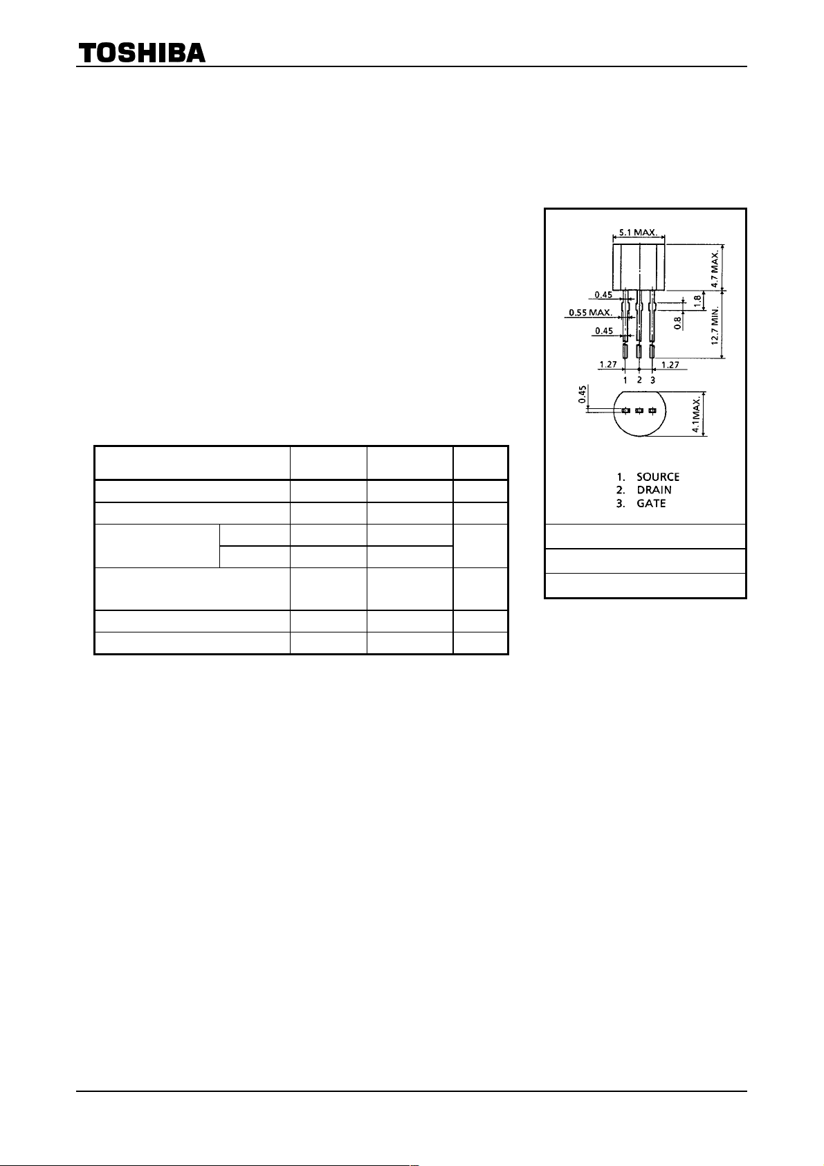
Unit: mm
JEDEC TO-92
JEITA SC-43
TOSHIBA 2-5F1H
Weight: 0.21 g (typ.)
1
2003-03-26
2SK982
<
Electrical Characteristics
Characteristics Symbol Test Condition Min Typ. Max Unit
Gate leakage current I
Drain cut-off current I
Drain-source breakdown voltage V
Gate threshold voltage Vth VDS = 10 V, ID = 1 mA 2 ¾ 3.5 V
Forward transfer admittance ïYfsï VDS = 10 V, ID = 50 mA 100 ¾ ¾ mS
Drain-source ON resistance R
Drain-source ON voltage V
Input capacitance C
Reverse transfer capacitance C
Output capacitance C
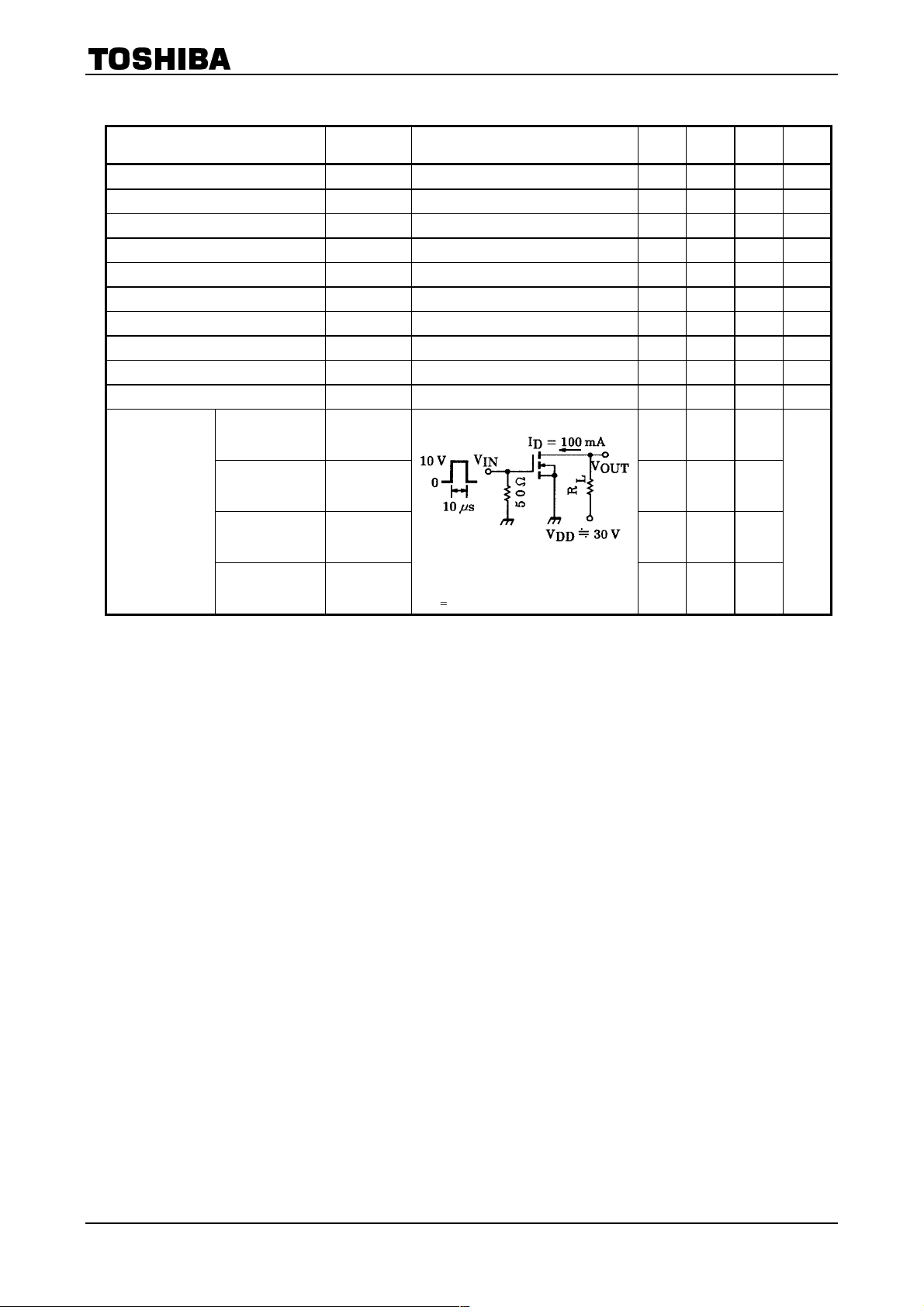
Rise time
Turn-on time
Switching time
Fall time
Turn-off Time
(Ta ==== 25°C)
(BR) DSSID
DS (ON)
DS (ON)
VGS = ±10 V, VDS = 0 ¾ ¾ ±100 nA
GSS
VDS = 60 V, VGS = 0 ¾ ¾ 10 mA
DSS
= 1 mA, VGS = 0 60 ¾ ¾ V
ID = 50 mA, VGS = 10 V ¾ 0.6 1.0 W
ID = 50 mA, VGS = 10 V ¾ 30 50 mV
VDS = 10 V, VGS = 0, f = 1 MHz ¾ 55 65 pF
iss
VDS = 10 V, VGS = 0, f = 1 MHz ¾ 13 18 pF
rss
VDS = 10 V, VGS = 0, f = 1 MHz ¾ 40 50 pF
oss
= 50 W)
out
¾ 75 ¾
tr ¾ 8 ¾
ton ¾ 14 ¾
tf ¾ 35 ¾
; tr, tf < 5 ns
V
t
off
IN
D.U
1% (Z
ns
Note: This transistor is the electrostatic sensitive device.
Please handle with caution.
2
2003-03-26
 Loading...