

Philips 2sk2232 DATASHEETS
2SK2232
TOSHIBA Field Effect Transistor Silicon N Channel MOS Type (L2−π−MOSV)
2SK2232
Chopper Regulator, DC−DC Converter and Motor Drive
Applications
4-V gate drive
Low drainsource ON resistance : R
High forward transfer admittance : |Y
Low leakage current : I
Enhancement mode : V
Maximum Ratings
Characteristics Symbol Rating Unit
Drain−source voltage V
Drain−gate voltage (RGS = 20 kΩ) V
Gate−source voltage V
Drain current
Drain power dissipation (Tc = 25°C) PD 35 W
Single pulse avalanche energy
(Note 2)
Avalanche current IAR 25 A
Repetitive avalanche energy (Note 3) EAR 3.5 mJ
Channel temperature Tch 150 °C
Storage temperature range T
(Ta = 25°C)
DC (Note 1) ID 25 A
Pulse (Note 1) I
= 100 µA (max) (VDS = 60 V)
DSS
= 0.8~2.0 V (VDS = 10 V, ID = 1 mA)
th
DSS
DGR
GSS
DP
E
AS
stg
= 36 m (typ.)
DS (ON)
| = 16 S (typ.)
fs
60 V
60 V
±20 V
100 A
156 mJ
−55~150 °C
Thermal Characteristics
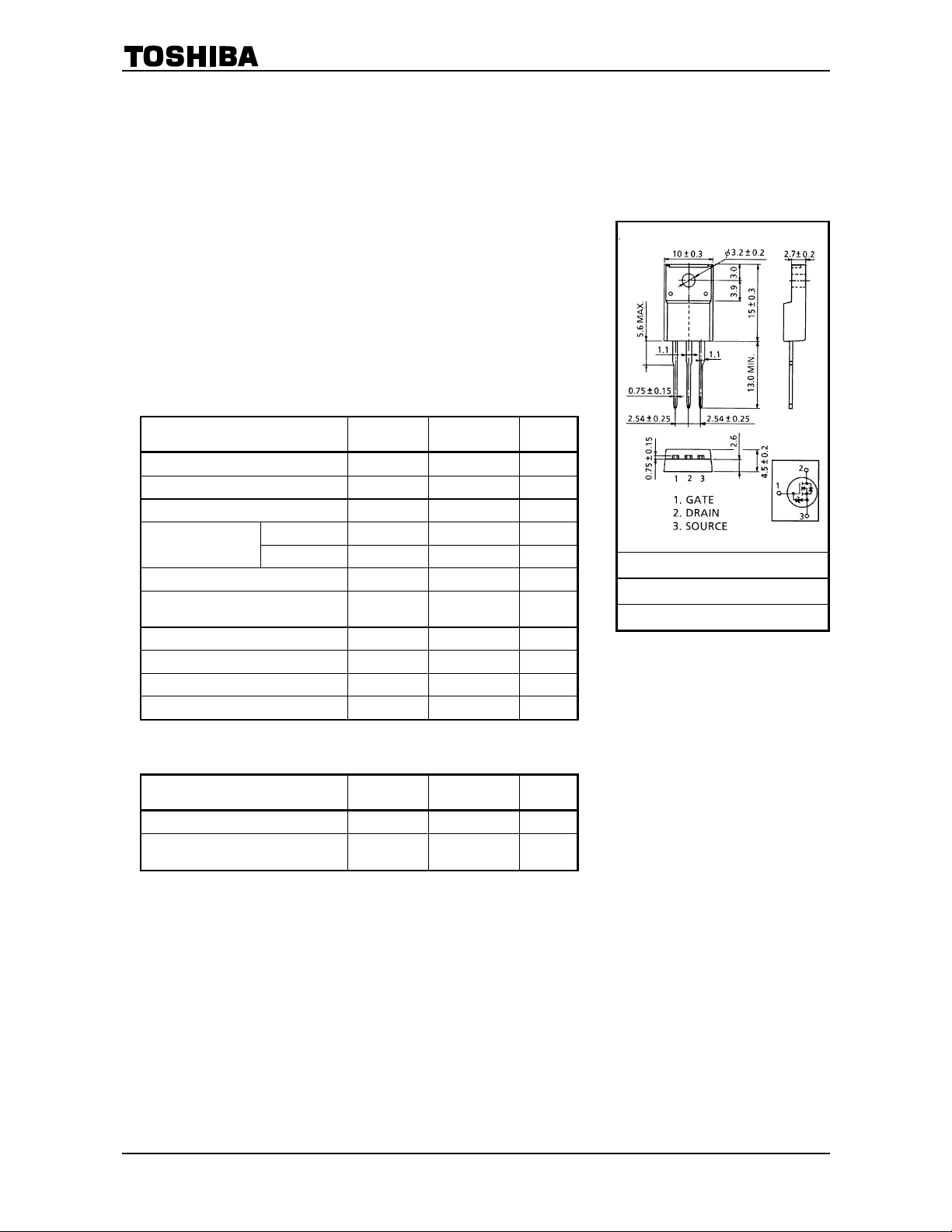
Unit: mm
JEDEC ―
JEITA SC-67
TOSHIBA 2-10R1B
Weight: 1.9 g (typ.)
Characteristics Symbol Max Unit
Thermal resistance, channel to case R
Thermal resistance, channel to
ambient
Note 1: Ensure that the channel temperature does not exceed 150°C..
Note 2: V
Note 3: Repetitive rating: pulse width limited by maximum channel temperature.
This transistor is an electrostatic-sensitive device.
Please handle with caution.
= 25 V, Tch = 25°C (initial), L = 339 µH, RG = 25 Ω, IAR = 25 A
DD
R
3.57 °C / W
th (ch−c)
62.5 °C / W
th (ch−a)
1
2004-07-06
2SK2232
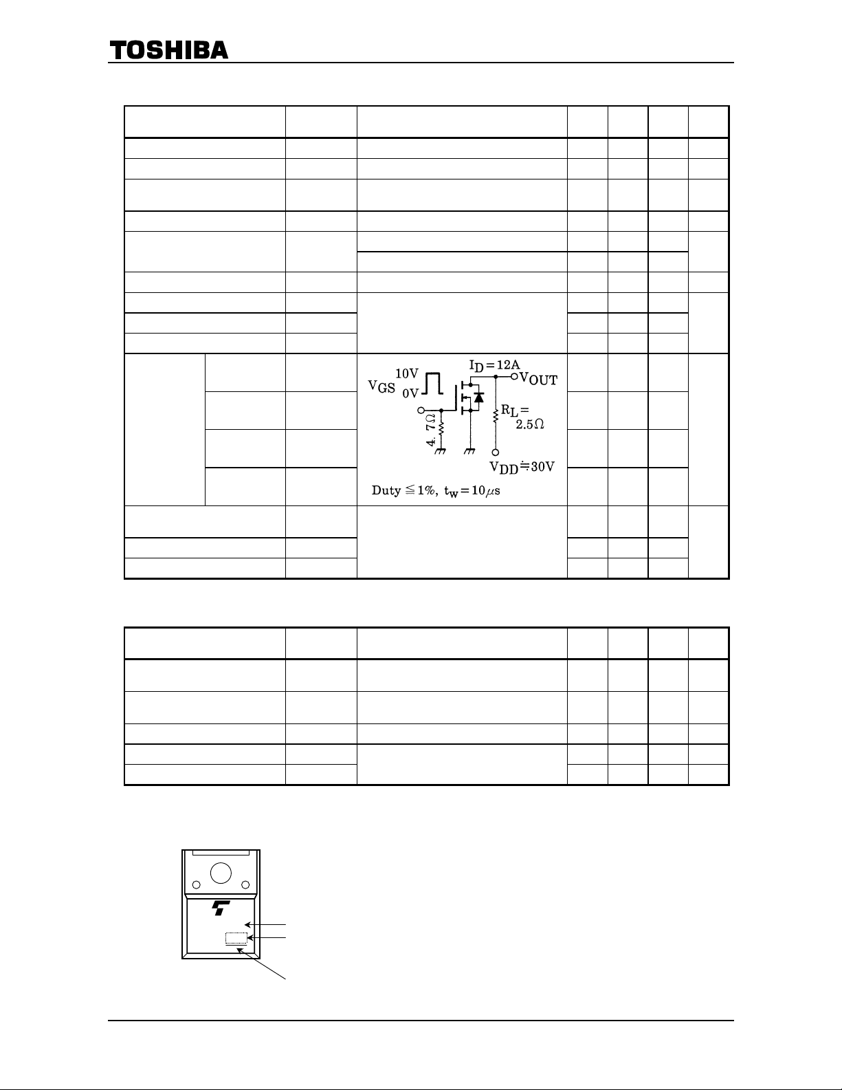
Electrical Characteristics
Characteristics Symbol Test Condition Min Typ. Max Unit
Gate leakage current I
Drain cut−off current I
Drain−source breakdown
voltage
Gate threshold voltage Vth VDS = 10 V, ID = 1 mA 0.8 — 2.0 V
Drain−source ON resistance R
Forward transfer admittance |Yfs| VDS = 10 V, ID = 12 A 10 16 — S
Input capacitance C
Reverse transfer capacitance C
Output capacitance C
Rise time tr — 20 —
Turn−on time ton — 30 —
Switching time
Fall time tf — 55 —
Turn−off time t
(Ta = 25°C)
GSS
DSS
V
(BR) DSS
DS (ON)
— 1000 —
iss
— 200 —
rss
oss
— 130 —
off
VGS = ±16 V, VDS = 0 V — — ±10 µA
VDS = 60 V, VGS = 0 V — — 100 µA
ID = 10 mA, VGS = 0 V 60 — — V
VGS = 4 V, ID = 12 A — 0.057 0.08
V
= 10 V, ID = 12 A — 0.036 0.046
GS
= 10 V, VGS = 0 V, f = 1 MHz
V
DS
— 550 —
Ω
pF
ns
Total gate charge (Gate−source
plus gate–drain)
Gate−source charge Qgs — 25 —
Gate−drain (“miller”) charge Qgd
— 38 —
Q
g
≈ 48 V, VGS = 10 V, ID = 25 A
V
DD
— 13 —
nC
Source−Drain Ratings and Characteristics
Characteristics Symbol Test Condition Min Typ. Max Unit
Continuous drain reverse current
(Note 1)
Pulse drain reverse current
(Note 1)
Forward voltage (diode) V
Reverse recovery time trr — 50 — ns
Reverse recovered charge Qrr
— — — 25 A
I
DR
I
— — — 100 A
DRP
IDR = 25 A, VGS = 0 V — — −1.8 V
DSF
= 25 A, VGS = 0 V, dI
I
DR
(Ta = 25°C)
/ dt = 50 A / µs
DR
— 35 — µC
Marking
K2232
Part No. (or abbreviation code)
Lot No.
A line indicates
lead (Pb)-free package or
lead (Pb)-free finish.
2
2004-07-06
 Loading...