

Philips 2sk2223 DATASHEETS
2SK2223-01R
N-channel MOS-FET
C
FUJI ELECTRIC GmbH; Lyoner Straße 26; D-60528 Frankfurt; Tel: 069-66 90 29-0; Fax: 069-66 90 29-56
FAP-IIA Series
500V 0,76Ω 10A 80W
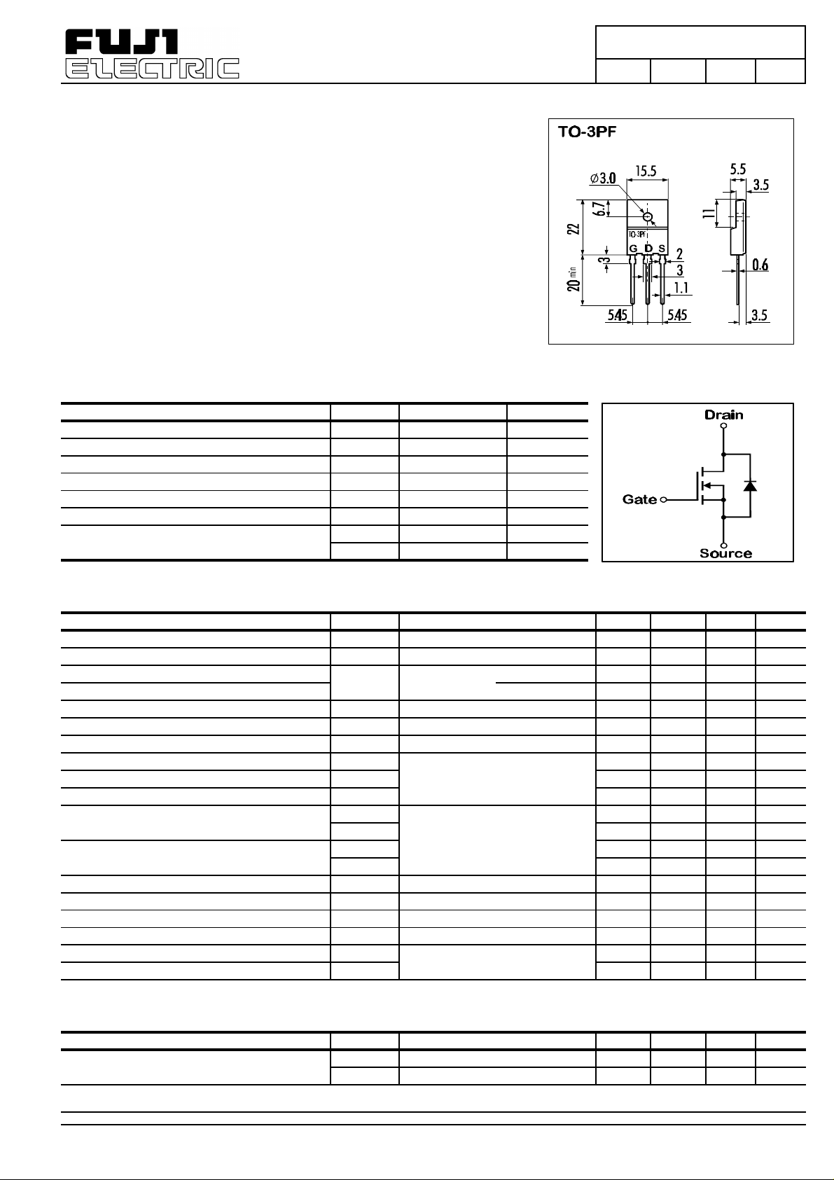
> Features > Outline Drawing
- High Speed Switching
- Low On-Resistance
- No Secondary Breakdown
- Low Driving Power
- High Voltage
GS = ± 30V Guarantee
- V
- Avalanche Proof
> Applications
- Switching Regulators
- UPS
- DC-DC converters
- General Purpose Power Amplifier
> Maximum Ratings and Characteristics > Equivalent Circuit
- Absolute Maximum Ratings (TC=25°C), unless otherwise specified
Item Symbol Rating Unit
Drain-Source-Voltage V
Drain-Gate-Voltage (RGS=20KΩ)
Continous Drain Current I
Pulsed Drain Current I
Gate-Source-Voltage V
Max. Power Dissipation P
Operating and Storage Temperature Range T
V
T
DS
DGR
D
D(puls)
GS
D
ch
stg
-55 ~ +150 °C
500 V
500 V
10 A
40 A
±30 V
80 W
150 °C
Electrical Characteristics (T
-
=25°C), unless otherwise specified
Item Symbol Test conditions Min. Typ. Max. Unit
Drain-Source Breakdown-Voltage V
Gate Threshhold Voltage V
Zero Gate Voltage Drain Current I
Gate Source Leakage Current I
Drain Source On-State Resistance R
Forward Transconductance g
Input Capacitance C
Output Capacitance C
Reverse Transfer Capacitance C
Turn-On-Time t
Turn-Off-Time t
(ton=t
on
d(on)+tr
off (ton=td(off)+tf
)
)
Avalanche Capability I
Continous Reverse Drain Current I
Pulsed Reverse Drain Current I
Diode Forward On-Voltage V
Reverse Recovery Time t
Reverse Recovery Charge Q
(BR)DSSID
GS(th)
DSS
GSS
DS(on)
fs
iss
oss
rss
t
d(on)
t
r
t
d(off)
t
f
AV
DR
DRM
SD
rr
rr
=1mA VGS=0V
ID=1mA V
DS=VGS
VDS=500V Tch=25°C
V
=0V Tch=125°C
GS
VGS=±30V VDS=0V
ID=5A VGS=10V
ID=5A VDS=25V
VDS=25V
VGS=0V
f=1MHz 35 50 pF
VCC=300V
ID=10A
VGS=10V
RGS=10 Ω
=25°C
L = 100µH
T
ch
TC=25°C
TC=25°C
IF=2xIDR VGS=0V Tch=25°C
IF=IDR VGS=0V
-dIF/dt=100A/µs Tch=25°C
500 V
2,5 3,0 3,5 V
10 500 µA
0,2 1,0 mA
10 100 nA
0,6 0,76
5 10 S
1500 2200 pF
160 240 pF
15 25 ns
40 60 ns
70 100 ns
60 90 ns
10 A
10 A
40 A
1,12 1,7 V
450 ns
3 µC
Ω
- Thermal Characteristics
Item Symbol Test conditions Min. Typ. Max. Unit
Thermal Resistance R
R
th(ch-a)
th(ch-c)
channel to air 30 °C/W
channel to case 1,56 °C/W
N-channel MOS-FET
FAP-IIA Series
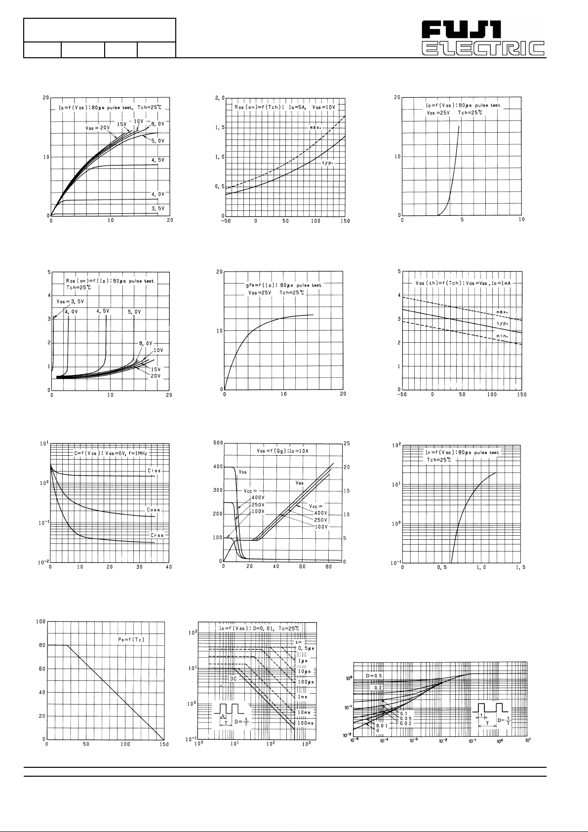
Typical Output Characteristics
Drain-Source-On-State Resistance vs. T
Typical Transfer Characteristics
→
→
→
Typical Drain-Source-On-State-Resistance vs. I
Typical Forward Transconductance vs. I
Gate Threshold Voltage vs. T
→
→
→
Typical Capacitance vs. V
Typical Input Charge
Forward Characteristics of Reverse Diode
→
→
→
Allowable Power Dissipation vs. T
Safe operation area
→
→
→
This specification is subject to change without notice!
500V 0,76Ω 10A 80W
> Characteristics
2SK2223-01R
ch
↑ 1 ↑ 2 ↑ 3
[A]
D
I
VDS [V]
↑ 4 ↑ 5 ↑ 6
]
Ω
[
DS(ON)
R
ID [A]
DS
]
Ω
[
DS(ON)
R
Tch [°C]
D
[S]
fs
g
ID [A]
D
[A]
D
I
[V]
GS(th)
V
VGS [V]
Tch [°C]
ch
↑ 7 ↑ 8 ↑ ↑ 9
C [nF]
VDS [V]
[V]
DS
V
Qg [nC]
C
[V]
GS
V
[A]
F
I
VSD [V]
↑
[K/W]
th(ch-c)
Z
Transient Thermal impedance
↑ 10 ↑ 12 11
[W]
D
P
Tc [°C]
[A]
D
I
VDS [V]
t [s]
 Loading...