

Philips 2sk168 DATASHEETS

Silicon N-Channel Junction FET
Application
VHF Amplifier, Mixer, Local oscillator
Outline
TO-92 (2)
2SK168
1. Gate
2. Source
3. Drain
3
2
1

2SK168
Absolute Maximum Ratings (Ta = 25°C)
Item Symbol Ratings Unit
Gate to drain voltage V
Gate to source voltage V
Gate current I
Drain current I
GDO
GSS
G
D
Channel power dissipation Pch 200 mW
Channel temperature Tch 150 °C
Storage temperature Tstg –55 to +150 °C
Electrical Characteristics (Ta = 25°C)
Item Symbol Min Typ Max Unit Test conditions
Gate to drain breakdown
V
(BR)GDO
voltage
Gate cutoff current I
Drain current I
Gate to source cutoff voltage V
GSS
DSS
GS(off)
Forward transfer admittance |yfs|810—mSV
Input capacitance Ciss — 6.8 — pF V
Reverse transfer capacitance Crss — 0.1 — pF V
Power gain PG — 27 — dB V
Noise figure NF — 1.7 — dB V
Note: 1. The 2SK168 is grouped by I
DEF
4 to 8 6 to 12 10 to 20
–30 — — V IG = –100 µA, IS = 0
— — –10 nA VGS = –0.5 V, VDS = 0
1
*
4 — 20 mA VDS = 5 V, VGS = 0
— — –3.0 V V
as follows.
DSS
–30 V
–1 V
10 mA
20 mA
= 5 V, ID = 10 µA
DS
= 5 V, VGS = 0, f = 1 kHz
DS
= 5 V, VGS = 0, f = 1 MHz
DS
= 5 V, VGS = 0, f = 1 MHz
DS
= 5 V, VGS = 0,
DS
f = 100 MHz
= 5 V, VGS = 0,
DS
f = 100 MHz
2
2SK168
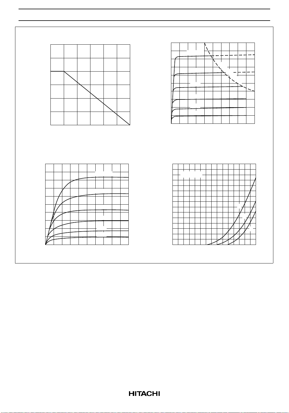
Maximum Channel Power
Dissipation Curve
300
200
100
Channel Power Dissipation Pch (mW)
0
50
100 150
Ambient Temperature Ta (°C)
Typical Output Characteristics (2)
10
VGS = 0
8
(mA)
D
6
–0.2 V
Typical Output Characteristics (1)
10
VGS = 0
8
(mA)
D
6
4
Drain Current I
2
0
10 20
Drain to Source Voltage V
Typical Transfer Characteristics
15
VDS = 5 V
10
(mA)
D
–0.2 V
–0.4
–0.6
–0.8
–1.0
Pch = 200 mW
30 40 50
(V)
DS
4
Drain Current I
2
0
12
Drain to Source Voltage V
–0.4
–0.6
–0.8
–1.0
345
(V)
DS
5
Drain Current I
0
–3.0 –2.0
Gate to Source Voltage V
F
E
D
–1.0 0
(V)
GS
3
 Loading...