

Philips 2sk1530 DATASHEETS
TOSHIBA Field Effect Transistor Silicon N Channel MOS Type
2SK1530
2SK1530
High Power Amplifier Application
l High breakdown voltage : V
l High forward transfer admittance : |Y
= 200V
DSS
| = 5.0 S (typ.)
fs
l Complementary to 2SJ201
Maximum Ratings
Characteristics Symbol Rating Unit
Drain−source voltage V
Gate−source voltage V
Drain current (Note 1) ID 12 A
Drain power dissipation (Tc = 25°C) PD 150 W
Channel temperature Tc 150 °C
Storage temperature range T
(Ta = 25°C)
200 V
DSS
±20 V
GSS
−55~150 °C
stg
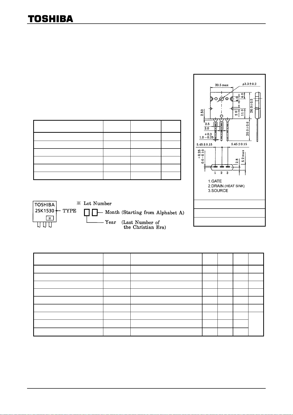
Marking
Unit: mm
JEDEC ―
JEITA ―
TOSHIBA 2-21F1B
Weight: 9.75 g (typ.)
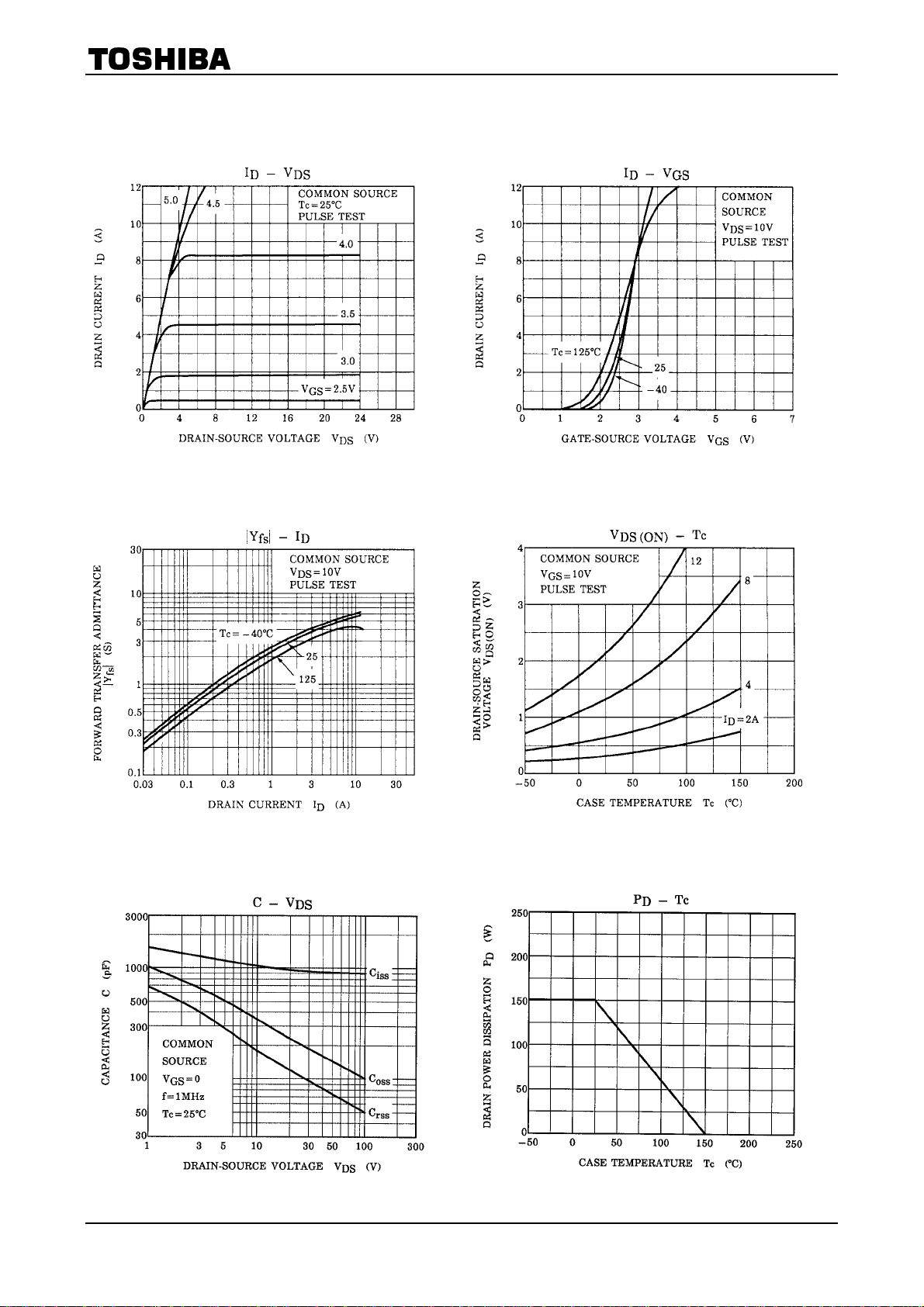
Electrical Characteristics
Characteristics Symbol Test Condition Min Typ. Max Unit
Drain cut−off current I
Gate leakage current I
Drain−source breakdown voltage V
Drain−source saturation voltage V
Gate−source cut−off voltage (Note 2) V
Forward transfer admittance |Yfs| VDS = 10 V, ID = 5 A — 5.0 — S
Input capacitance C
Output capacitance C
Reverse transfer capacitance C
(Ta = 25°C)
(BR) DSSID
DS (ON)
GS (OFF)
VDS = 200 V, VGS = 0 — — 1.0 mA
DSS
VDS = 0V, VGS = ±20 V — — ±0.5 µA
GSS
= 10 mA, VGS = 0 200 — — V
ID = 8 A, V
VDS = 10 V, ID = 0.1 A 0.8 — 2.8 V
VDS = 30 V, VGS = 0, f = 1 MHz — 900 —
iss
VDS = 30 V, VGS = 0, f = 1 MHz — 180 —
oss
V
rss
= 30 V, VGS = 0, f = 1 MHz — 100 —
DD
= 10 V — 2.5 5.0 V
GS
Note 1: Please use devices on condition that the channel temperature is below 150°C.
Note 2: V
GS (OFF)
Classification 0: 0.8~1.6 Y: 1.4~2.8
This transistor is an electrostatic sensitive device.
Please handle with caution.
pF
1
2002-09-02
2SK1530
2
2002-09-02
 Loading...