

Philips 2sk117 DATASHEETS
TOSHIBA Field Effect Transistor Silicon N Channel Junction Type
2SK117
2SK117
Low Noise Audio Amplifier Applications
• High |Y
• High breakdown voltage: V
• Low noise: NF = 1.0dB (typ.)
(VDS = 10 V, ID = 0.5 mA, f = 1 kHz, RG = 1 kΩ)
• High input impedance: I
Maximum Ratings
Gate-drain voltage V
Gate current IG 10 mA
Drain power dissipation PD 300 mW
Junction temperature T
Storage temperature range T
Electrical Characteristics
|: |Yfs| = 15 mS (typ.) (VDS = 10 V, VGS = 0)
fs
= −50 V
GDS
= −1 nA (max) (VGS = −30 V)
GSS
(Ta ==== 25°C)
Characteristics Symbol Rating Unit
GDS
j
stg
(Ta ==== 25°C)
−50 V
125 °C
−55~125 °C
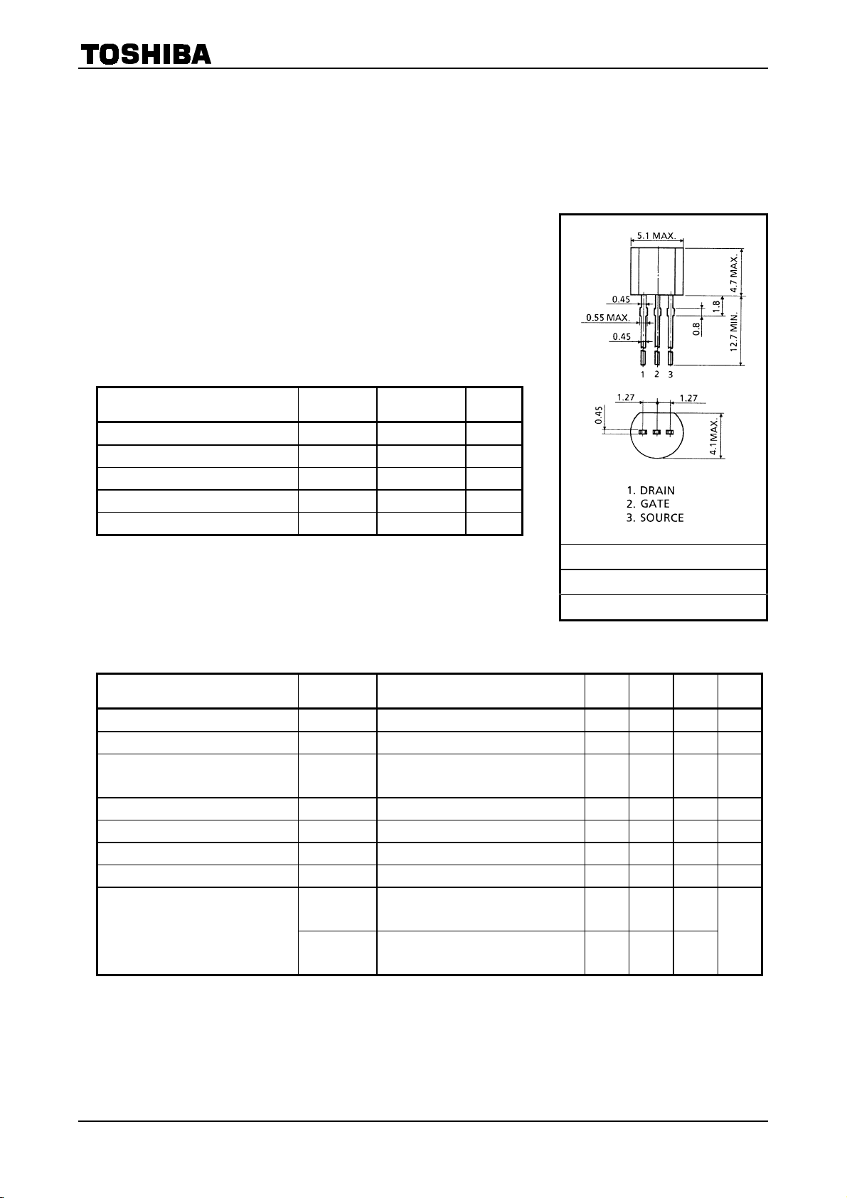
Unit: mm
JEDEC TO-92
JEITA SC-43
TOSHIBA 2-5F1D
Weight: 0.21 g (typ.)
Characteristics Symbol Test Condition Min Typ. Max Unit
Gate cut-off current I
Gate-drain breakdown voltage V
Drain current
Gate-source cut-off voltage V
Forward transfer admittance Y
Input capacitance C
Reverse transfer capacitance C
Noise figure
Note: I
classification Y: 1.2~3.0 mA, GR: 2.6~6.5 mA, BL: 6~14 mA
DSS
GSS
(BR) GDS
I
DSS
GS (OFF)
fs
iss
rss
NF (1)
NF (2)
VGS = −30 V, VDS = 0 −1.0 nA
VDS = 0, IG = −100 µA −50 V
(Note)
V
VDS = 10 V, VGS = 0, f = 1 MHz 13 pF
VGD = −10 V, ID = 0, f = 1 MHz 3 pF
= 10 V, VGS = 0 1.2 14 mA
V
DS
VDS = 10 V, ID = 0.1 µA −0.2 −1.5 V
= 10 V, VGS = 0, f = 1 kHz 4.0 15 mS
DS
V
= 10 V, RG = 1 kΩ
DS
I
= 0.5 mA, f = 10 Hz
D
V
= 10 V, RG = 1 kΩ
DS
= 0.5 mA, f = 1 kHz
I
D
5 10
1 2
dB
1
2003-03-25
2SK117
2
2003-03-25
 Loading...