

Philips 2sd1609 DATASHEETS
2SD1609, 2SD1610
Silicon NPN Epitaxial
Application
Low frequency high voltage amplifier complementary pair with 2SB1109 and 2SB1110
Outline
TO-126 MOD
1. Emitter
2. Collector
1
2
3
3. Base
Absolute Maximum Ratings (Ta = 25°C)
Ratings
Item Symbol 2SD1609 2SD1610 Unit
Collector to base voltage V
Collector to emitter voltage V
Emitter to base voltage V
Collector current I
Collector power dissipation P
Junction temperature Tj 150 150 °C
Storage temperature Tstg –45 to +150 –45 to +150 °C
CBO
CEO
EBO
C
C
160 200 V
160 200 V
55V
100 100 mA
1.25 1.25 W
2SD1609, 2SD1610
Electrical Characteristics (Ta = 25°C)
2SD1609 2SD1610
Item Symbol Min Typ Max Min Typ Max Unit Test conditions
Collector to base
breakdown voltage
Collector to emitter
breakdown voltage
Emitter to base
breakdown voltage
Collector cutoff current I
DC current tarnsfer ratio h
Base to emitter voltage V
Collector to emitter
saturation voltage
Gain bandwidth product f
Collector output
capacitance
Note: 1. The 2SD1609 and 2SD1610 are grouped by h
V
(BR)CBO
V
(BR)CEO
V
(BR)EBO
CBO
160 — — 200 — — V IC = 10 µA, IE = 0
160 — — 200 — — V IC = 1 mA, RBE = ∞
5——5——VIE = 10 µA, IC = 0
——10———µAVCB = 140 V, IE = 0
—————10 VCB = 160 V, IE = 0
1
*
60 — 320 60 — 320 VCE = 5 V, IC = 10 mA
30 — — 30 — — VCE = 5 V, IC = 1 mA
— — 1.5 — — 1.5 V VCE = 5 V, IC = 10 mA
——2 ——2 V IC = 30 mA, IB = 3 mA
— 140 — — 140 — MHz VCE = 5 V, IC = 10 mA
h
V
FE1
FE2
BE
CE(sat)
T
Cob — 3.8 — — 3.8 — pF VCB = 10 V, IE = 0,
f = 1 MHz
as follows.
FE1
BCD
60 to 120 100 to 200 160 to 320
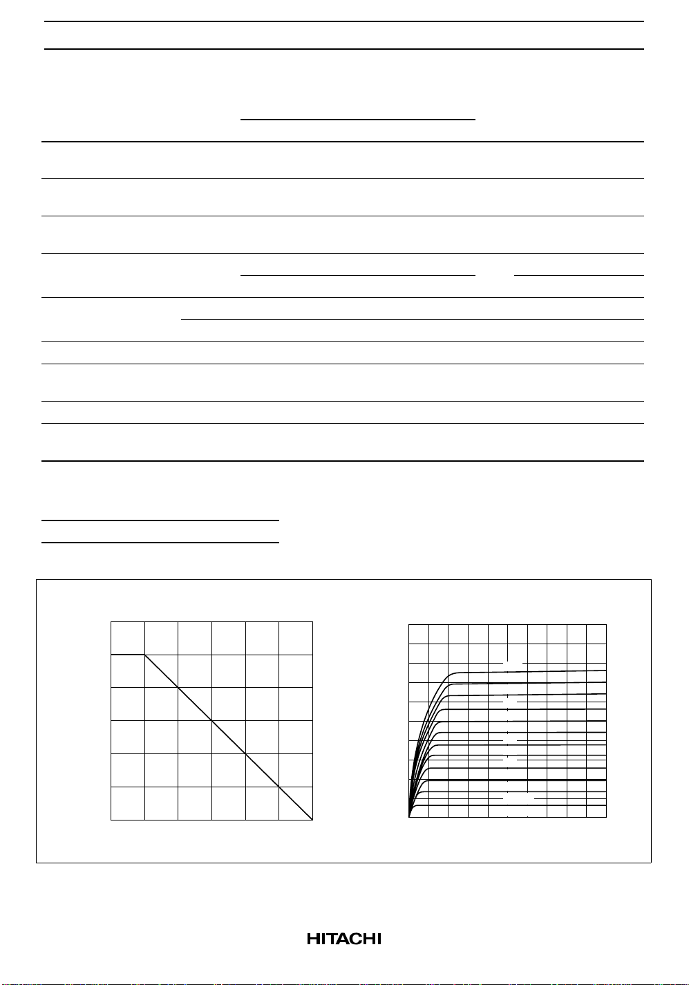
Maximum Collector Dissipation
1.5
(W)
C
1.0
0.5
Collector power dissipation P
0 50 100 150
Ambient temperature Ta (°C)
Curve
Typical Output Characteristics
20
16
(mA)
C
12
8
4
Collector current I
024
Collector to emitter voltage V
120
110
100
90
80
70
60
50
40
30
20
10 µA
IB = 0
CE
1086
(V)
2
100
50
(mA)
C
20
10
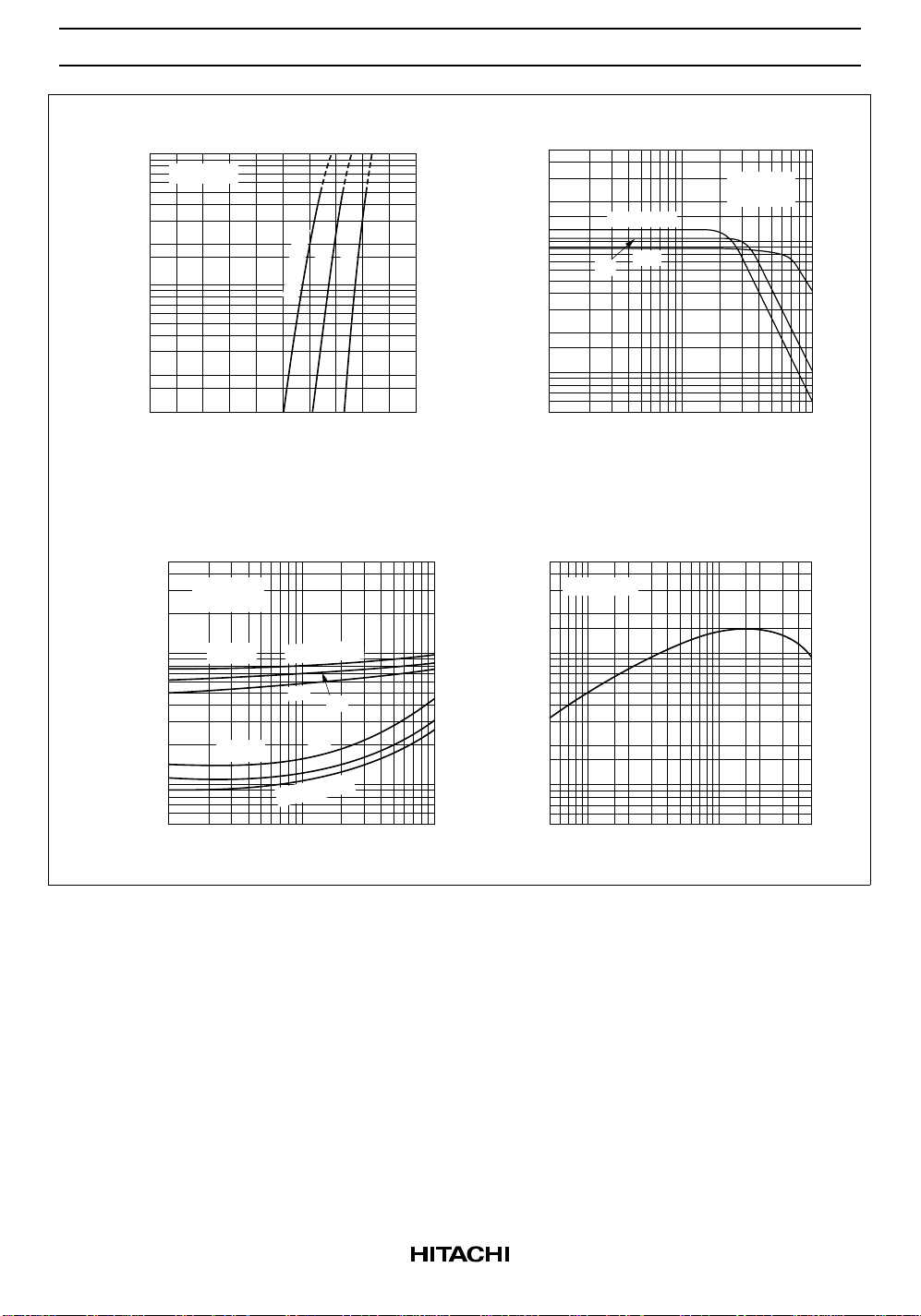
Typical Transfer Characteristics
VCE = 5 V
25
–25
Ta = 75°C
FE
500
200
100
50
2SD1609, 2SD1610
DC Current Transfer Ratio vs.
Collector Current
VCE = 5 V
Pulse
Ta = 75°C
–25
25
5
Collector current I
2
1
0 0.2
Base to emitter voltage V
0.4
0.6 1.00.8
BE
Saturation Voltage vs. Collector Current
5
(V)
(V)
CE(sat)
BE(sat)
Base to emitter saturation voltage V
0.05
Collector to emitter saturation voltage V
IC = 10 I
B
Pulse
2
1.0
V
BE(sat)
0.5
0.2
0.1
V
CE(sat)
Ta = –25°C
12 10
55020 100
Collector current I
Ta = –25°C
75
25
75
25
(mA)
C
(V)
20
DC current transfer ratio h
10
5
1 2 20 10010 50
5
Collector current I
Gain Bandwidth Product vs.
Collector Current
500
VCE = 10 V
200
(MHz)
T
100
50
20
10
Gain bandwidth product f
5
1.00.5 2
Collector current I
(mA)
C
(mA)
C
2010 505
3
 Loading...