Philips 2sc3074 DATASHEETS

TOSHIBA Transistor Silicon NPN Epitaxial Type (PCT process)
2SC3074
2SC3074
High Current Switching Applications
· Low collector saturation voltage: V
· High speed switching time: t
· Complementary to 2SA1244
Maximum Ratings
Characteristics Symbol Rating Unit
Collector-base voltage V
Collector-emitter voltage V
Emitter-base voltage V
Collector current IC 5 A
Base current IB 1 A
Collector power
dissipation
Junction temperature Tj 150 °C
Storage temperature range T
(Ta = 25°C)
Ta = 25°C 1.0
Tc = 25°C
CE (sat)
= 1.0 µs (typ)
stg
= 0.4 V (max) (IC = 3 A)
60 V
CBO
50 V
CEO
5 V
EBO
P
C
−55 to 150 °C
stg
20
W
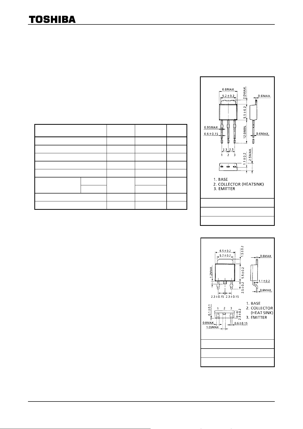
Unit: mm
JEDEC ―
JEITA ―
TOSHIBA 2-7B1A
Weight: 0.36 g (typ.)
JEDEC ―
JEITA ―
TOSHIBA 2-7J1A
Weight: 0.36 g (typ.)
1
2002-07-23

2SC3074
Electrical Characteristics
Characteristics Symbol Test Condition Min Typ. Max Unit
Collector cut-off current I
Emitter cut-off current I
Collector-emitter breakdown voltage V
DC current gain
Collector-emitter saturation voltage V
Base-emitter saturation voltage V
Transition frequency fT VCE = 4 V, IC = 1 A ― 120 ― MHz
Collector output capacitance Cob VCB = 10 V, IE = 0, f = 1 MHz ― 80 ― pF
Turn-on time ton ― 0.1 ―
Switching time
Storage time t
Fall time t
(Ta = 25°C)
(BR) CEOIC
h
FE (1)
h
FE (2)
CE (sat)
BE (sat)
VCB = 50 V, IE = 0 ― ― 1 µA
CBO
VEB = 5 V, IC = 0 ― ― 1 µA
EBO
= 10 mA, IB = 0 50 ― ― V
V
= 1 V, IC = 1 A 70 ― 240
(Note)
― 1.0 ―
stg
f
CE
VCE = 1 V, IC = 3 A 30 ― ―
IC = 3 A, IB = 0.15 A ― 0.2 0.4 V
IC = 3 A, IB = 0.15 A ― 0.9 1.2 V
V
CC
OUTPUT
10 Ω
= 30 V
― 0.1 ―
20 µs
INPUT
B1
I
I
= −IB2 = 0.15 A,
B1
DUTY CYCLE ≤ 1%
I
B2
I
B1
I
B2
µs
Note: h
classification O: 70 to 140, Y: 120 to 240
FE (1)
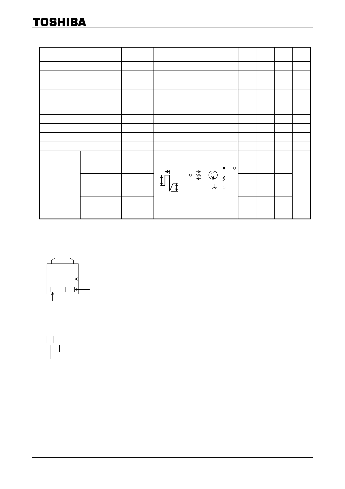
Marking
C3074 Product No.
Lot No.
hFE Classification
Explanation of Lot No.
Month of manufacture: January to December are denoted by letters A to L respectively.
Year of manufacture: last decimal digit of the year of manufacture
2
2002-07-23
 Loading...