

Philips 2PC1815Y, 2PC1815GR Datasheet
DATA SH EET
Product specification
Supersedes data of 1997 Mar 28
1999 May 28
DISCRETE SEMICONDUCTORS
2PC1815
NPN general purpose transistor
ook, halfpage
M3D186

1999 May 28 2
Philips Semiconductors Product specification
NPN general purpose transistor 2PC1815
FEATURES
• Low current (max. 150 mA)
• Low voltage (max. 50 V).
APPLICATIONS
• General purpose switching and amplification,
e.g. audio amplifier driver stages.
DESCRIPTION
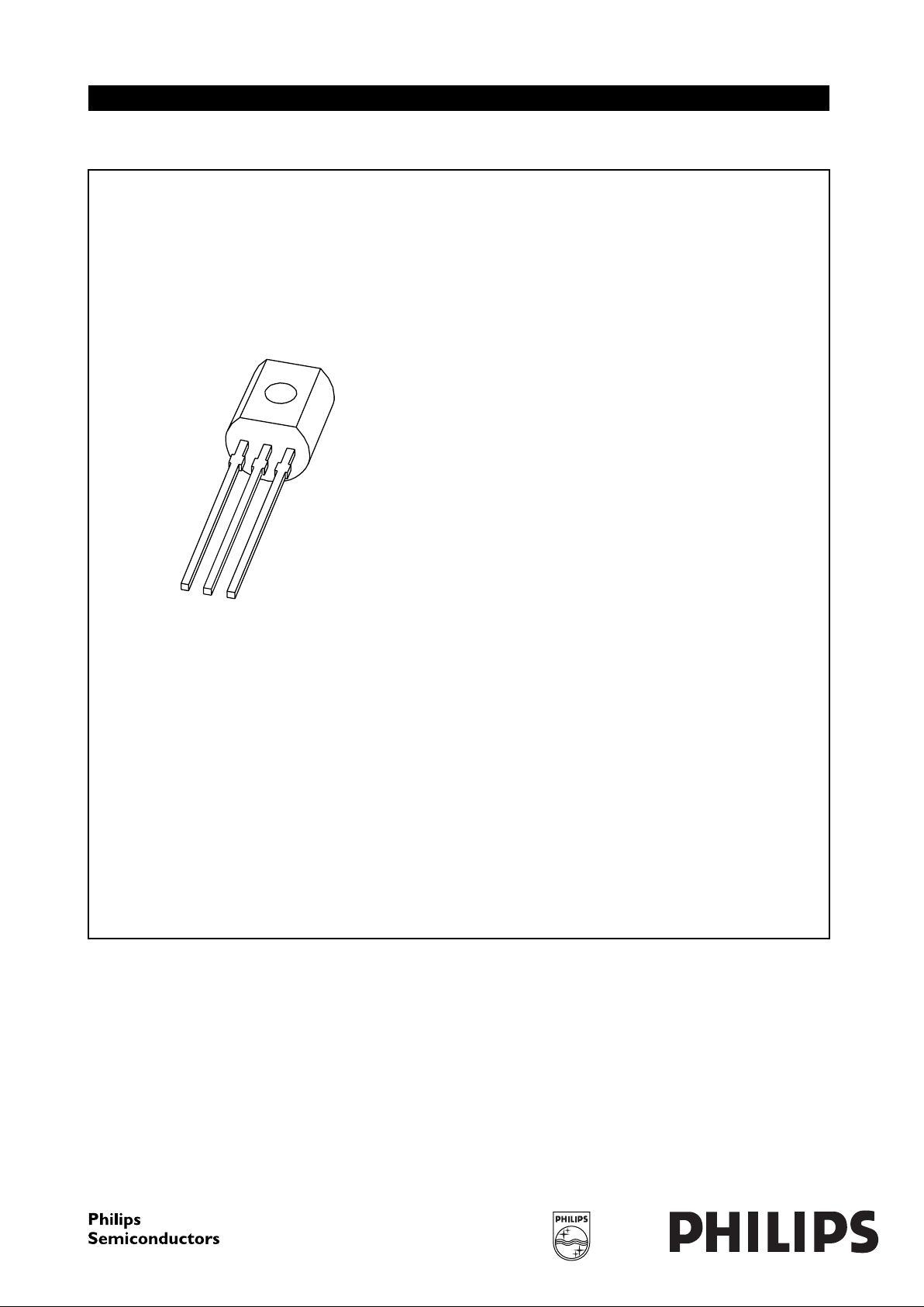
NPN transistor in a TO-92 (SOT54) plastic package.
PNP complement: 2PA1015.
PINNING
PIN DESCRIPTION
1 base
2 collector
3 emitter
Fig.1 Simplified outline (TO-92; SOT54)
and symbol.
handbook, halfpage
1
3
2
MAM259
2
1
3
LIMITING VALUES
In accordance with the Absolute Maximum Rating System (IEC 134).
Note
1. Transistor mounted on an FR4 printed-circuit board.
SYMBOL PARAMETER CONDITIONS MIN. MAX. UNIT
V
CBO
collector-base voltage open emitter − 60 V
V
CEO
collector-emitter voltage open base − 50 V
V
EBO
emitter-base voltage open collector − 5V
I
C
collector current (DC) − 150 mA
I
CM
peak collector current − 200 mA
I
BM
peak base current − 200 mA
P
tot
total power dissipation T
amb
≤ 25 °C; note 1 − 500 mW
T
stg
storage temperature −65 +150 °C
T
j
junction temperature − 150 °C
T
amb
operating ambient temperature −65 +150 °C

1999 May 28 3
Philips Semiconductors Product specification
NPN general purpose transistor 2PC1815
THERMAL CHARACTERISTICS
Note
1. Transistor mounted on an FR4 printed-circuit board.
CHARACTERISTICS
T
j
=25°C unless otherwise specified.
SYMBOL PARAMETER CONDITIONS VALUE UNIT
R
th j-a
thermal resistance from junction to ambient note 1 250 K/W
SYMBOL PARAMETER CONDITIONS MIN. TYP. MAX. UNIT
I
CBO
collector cut-off current IE= 0; VCB=60V −−100 nA
I
EBO
emitter cut-off current IC= 0; VEB=5V −−100 nA
h
FE
DC current gain IC= 150 mA; VCE=6V 25 −−
h
FE
DC current gain IC= 2 mA; VCE=6V
2PC1815 120 − 700
2PC1815Y 120 − 240
2PC1815GR 200 − 400
2PC1815BL 350 − 700
V
CEsat
collector-emitter saturation voltage IC= 100 mA; IB=10mA −−300 mV
V
BEsat
base-emitter saturation voltage IC= 100 mA; IB=10mA −−1.1 V
C
c
collector capacitance IE=ie= 0; VCB= 10 V; f = 1 MHz − 2.5 3.5 pF
f
T
transition frequency IC= 1 mA; VCE= 6 V; f = 100 MHz 80 −−MHz
F noise figure I
C
= 200 µA; VCE=5V;
RS=2kΩ; f = 1 kHz
−−10 dB
 Loading...