

Philips 2PA1774JS, 2PA1774JR, 2PA1774JQ Datasheet
DISCRETE SEMICONDUCTORS
DATA SH EET
M3D425
2PA1774J
PNP general purpose transistor
Preliminary specification
Supersedes data of 1998 Nov 10
1999 May 04
Philips Semiconductors Preliminary specification
PNP general purpose transistor 2PA1774J
FEATURES
• Power dissipation comparable to SOT23
• Low output capacitance
• Low saturation voltage V
CEsat
• Low current (max. 100 mA)
• Low voltage (max. 50 V).
APPLICATIONS
• General purpose switching and amplification in
miniaturized application areas such as telecom and
multimedia.
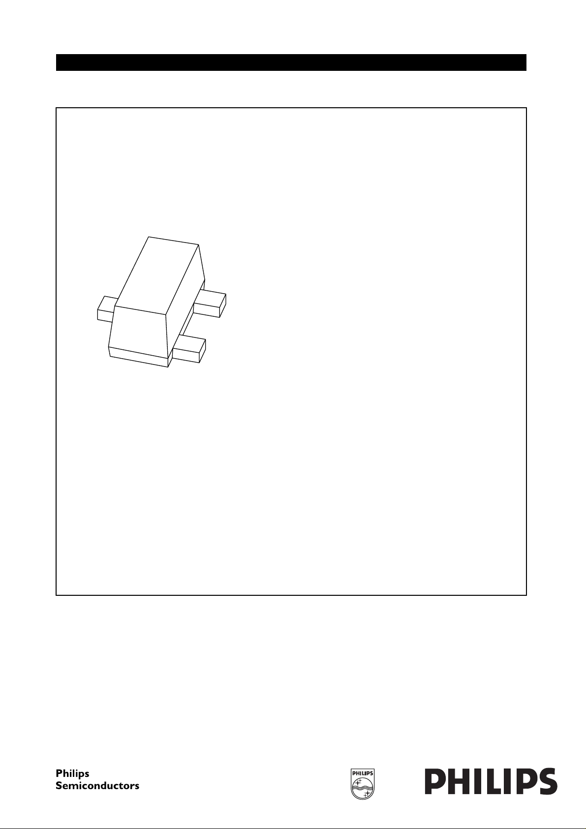
DESCRIPTION
PNP transistor encapsulated in an ultra small plastic
SMD SC-89 (SOT490) package.
NPN complement: 2PC4617J.
MARKING
TYPE NUMBER MARKING CODE
2PA1774JQ YQ
2PA1774JR YR
2PA1774JS YS
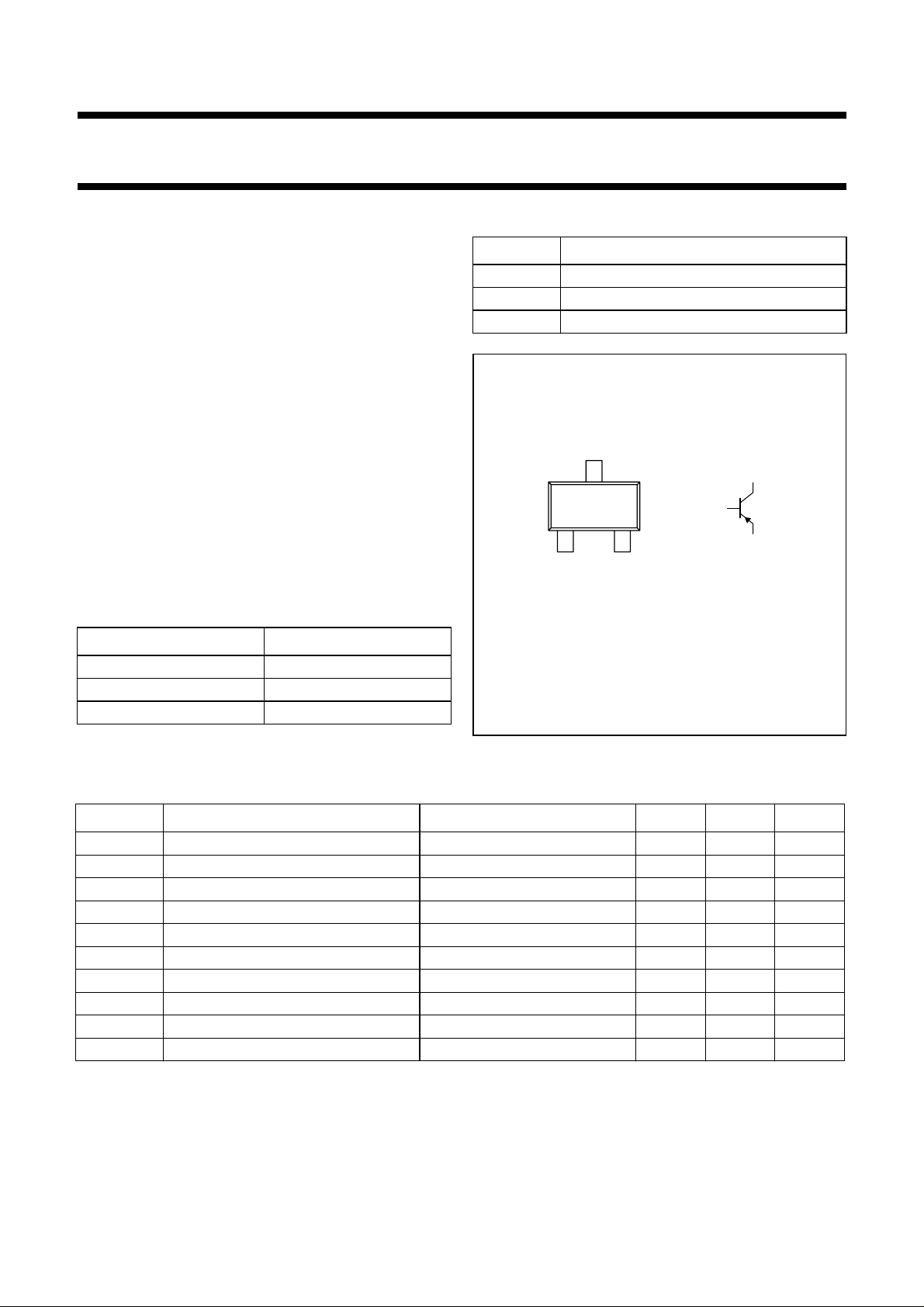
PINNING
PIN DESCRIPTION
1 base
2 emitter
3 collector
handbook, halfpage
12
Top view
3
1
MAM411
Fig.1 Simplified outline (SC-89; SOT490) and
symbol.
3
2
LIMITING VALUES
In accordance with the Absolute Maximum Rating System (IEC 134).
SYMBOL PARAMETER CONDITIONS MIN. MAX. UNIT
V
CBO
V
CEO
V
EBO
I
C
I
CM
I
BM
P
tot
T
stg
T
j
T
amb
collector-base voltage open emitter −−50 V
collector-emitter voltage open base −−50 V
emitter-base voltage open collector −−5V
collector current (DC) −−100 mA
peak collector current −−200 mA
peak base current −−100 mA
total power dissipation T
≤ 25 °C; note 1 − 250 mW
amb
storage temperature −65 +150 °C
junction temperature − 150 °C
operating ambient temperature −65 +150 °C
Note
1. Refer to SC-89 (SOT490) standard mounting conditions.
1999 May 04 2
Philips Semiconductors Preliminary specification
PNP general purpose transistor 2PA1774J
THERMAL CHARACTERISTICS
SYMBOL PARAMETER CONDITIONS MAX. UNIT
R
th j-a
Note
1. Refer to SC-89 (SOT490) standard mounting conditions.
CHARACTERISTICS
=25°C unless otherwise specified.
T
amb
SYMBOL PARAMETER CONDITIONS MIN. MAX. UNIT
I
CBO
I
EBO
h
FE
V
CEsat
C
c
f
T
thermal resistance from junction to ambient in free air; note 1 500 K/W
collector cut-off current IE= 0; VCB= −30 V −−100 nA
I
= 0; VCB= −30 V; Tj= 150 °C −−5µA
E
emitter cut-off current IC= 0; VEB= −4V −−100 nA
DC current gain IC= −1 mA; VCE= −6 V; note 1
2PA1774JQ 120 270
2PA1774JR 180 390
2PA1774JS 270 560
collector-emitter saturation
IC= −50 mA; IB= −5 mA; note 1 −−200 mV
voltage
collector capacitance IE=ie= 0; VCB= −12 V; f = 1 MHz − 2.2 pF
transition frequency IC= −2 mA; VCE= −12 V;
100 − MHz
f = 100 MHz; note 1
Note
1. Pulse test: t
≤ 300 µs; δ≤0.02.
p
1999 May 04 3
 Loading...