

Philips 2pa1774 DATASHEETS
DISCRETE SEMICONDUCTORS
DATA SH EET
M3D173
2PA1774
PNP general purpose transistor
Preliminary specification
Supersedes data of 1997 Jul 09
1999 Jun 01
Philips Semiconductors Preliminary specification
PNP general purpose transistor 2PA1774
FEATURES
• Low current (max. 100 mA)
• Low voltage (max. 40 V).
APPLICATIONS
• General purpose switching and amplification in
communication, electronic data processing (EDP) and
consumer applications.
DESCRIPTION
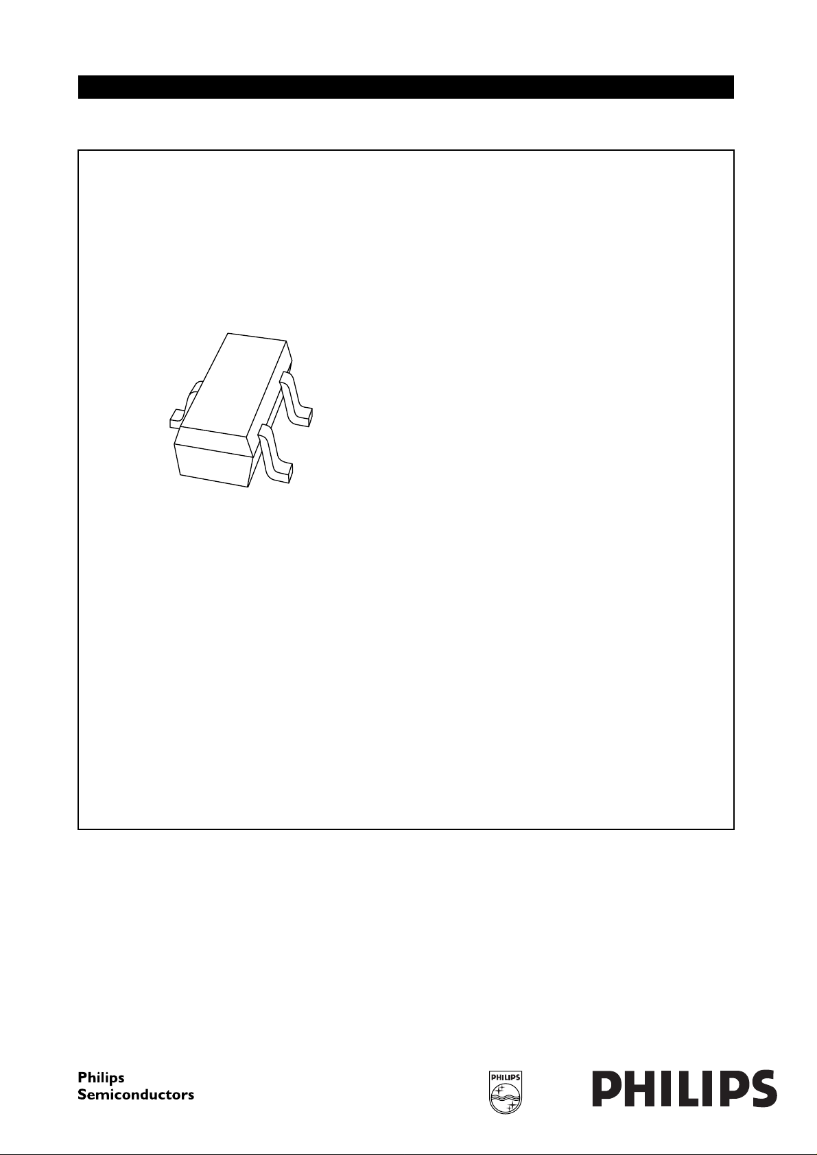
PNP transistor in an SC-75 plastic package.
NPN complement: 2PC4617.
MARKING
TYPE NUMBER MARKING CODE
2PA1774Q YQ
2PA1774R YR
2PA1774S YS
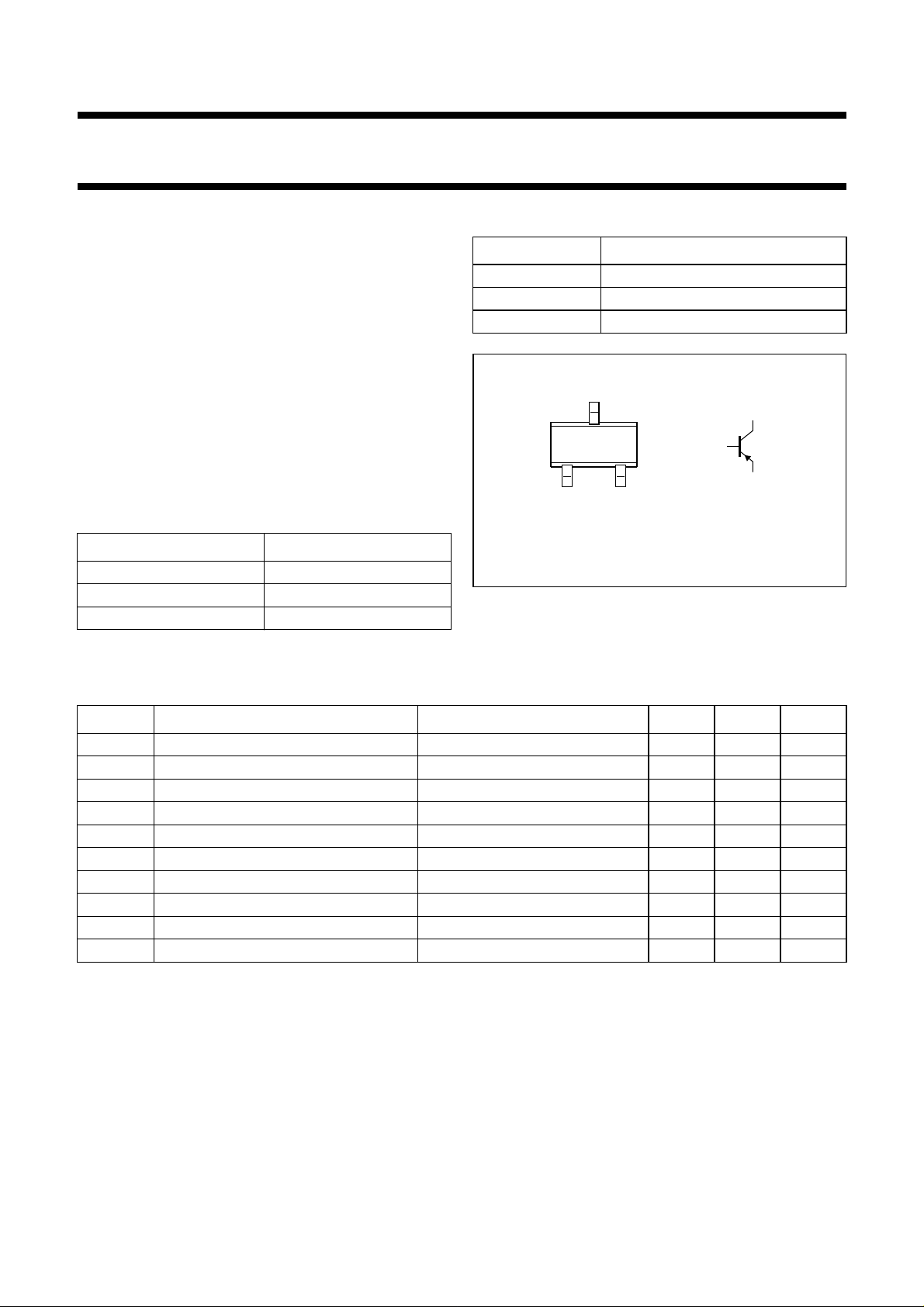
PINNING
PIN DESCRIPTION
1 base
2 emitter
3 collector
handbook, halfpage
12
Top view
3
Fig.1 Simplified outline (SC-75) and symbol.
3
1
2
MAM362
LIMITING VALUES
In accordance with the Absolute Maximum Rating System (IEC 134).
SYMBOL PARAMETER CONDITIONS MIN. MAX. UNIT
V
CBO
V
CEO
V
EBO
I
C
I
CM
I
BM
P
tot
T
stg
T
j
T
amb
collector-base voltage open emitter −−50 V
collector-emitter voltage open base −−40 V
emitter-base voltage open collector −−5V
collector current (DC) −−100 mA
peak collector current −−200 mA
peak base current −−100 mA
total power dissipation T
≤ 25 °C; note 1 − 150 mW
amb
storage temperature −65 +150 °C
junction temperature − 150 °C
operating ambient temperature −65 +150 °C
Note
1. Transistor mounted on an FR4 printed-circuit board.
1999 Jun 01 2
Philips Semiconductors Preliminary specification
PNP general purpose transistor 2PA1774
THERMAL CHARACTERISTICS
SYMBOL PARAMETER CONDITIONS VALUE UNIT
R
th j-a
Note
1. Transistor mounted on an FR4 printed-circuit board.
CHARACTERISTICS
=25°C unless otherwise specified.
T
amb
SYMBOL PARAMETER CONDITIONS MIN. MAX. UNIT
I
CBO
I
EBO
h
FE
V
CEsat
C
c
f
T
thermal resistance from junction to ambient note 1 833 K/W
collector cut-off current IE= 0; VCB= −30 V −−100 nA
I
= 0; VCB= −30 V; Tj= 150 °C −−5µA
E
emitter cut-off current IC= 0; VEB= −4V −−100 nA
DC current gain IC= −1 mA; VCE= −6 V; note 1
2PA1774Q 120 270
2PA1774R 180 390
2PA1774S 270 560
collector-emitter saturation voltage IC= −50 mA; IB= −5 mA; note 1 −−200 mV
collector capacitance IE=ie= 0; VCB= −12 V; f = 1 MHz − 2.2 pF
transition frequency IE= −2 mA; VCE= −12 V; f = 100 MHz;
100 − MHz
note 1
Note
1. Pulse test: t
≤ 300 µs; δ≤0.02.
p
1999 Jun 01 3
 Loading...